US6765227B1 - Semiconductor-on-insulator (SOI) wafer having a Si/SiGe/Si active layer and method of fabrication using wafer bonding - Google Patents
Semiconductor-on-insulator (SOI) wafer having a Si/SiGe/Si active layer and method of fabrication using wafer bondingDownload PDFInfo
- Publication number
- US6765227B1 US6765227B1US10/116,791US11679102AUS6765227B1US 6765227 B1US6765227 B1US 6765227B1US 11679102 AUS11679102 AUS 11679102AUS 6765227 B1US6765227 B1US 6765227B1
- Authority
- US
- United States
- Prior art keywords
- silicon
- layer
- germanium
- wafer according
- soi wafer
- Prior art date
- Legal status (The legal status is an assumption and is not a legal conclusion. Google has not performed a legal analysis and makes no representation as to the accuracy of the status listed.)
- Expired - Lifetime, expires
Links
Images


Classifications
- H—ELECTRICITY
- H10—SEMICONDUCTOR DEVICES; ELECTRIC SOLID-STATE DEVICES NOT OTHERWISE PROVIDED FOR
- H10D—INORGANIC ELECTRIC SEMICONDUCTOR DEVICES
- H10D30/00—Field-effect transistors [FET]
- H10D30/01—Manufacture or treatment
- H10D30/021—Manufacture or treatment of FETs having insulated gates [IGFET]
- H10D30/031—Manufacture or treatment of FETs having insulated gates [IGFET] of thin-film transistors [TFT]
- H—ELECTRICITY
- H01—ELECTRIC ELEMENTS
- H01L—SEMICONDUCTOR DEVICES NOT COVERED BY CLASS H10
- H01L21/00—Processes or apparatus adapted for the manufacture or treatment of semiconductor or solid state devices or of parts thereof
- H01L21/70—Manufacture or treatment of devices consisting of a plurality of solid state components formed in or on a common substrate or of parts thereof; Manufacture of integrated circuit devices or of parts thereof
- H01L21/71—Manufacture of specific parts of devices defined in group H01L21/70
- H01L21/76—Making of isolation regions between components
- H01L21/762—Dielectric regions, e.g. EPIC dielectric isolation, LOCOS; Trench refilling techniques, SOI technology, use of channel stoppers
- H01L21/7624—Dielectric regions, e.g. EPIC dielectric isolation, LOCOS; Trench refilling techniques, SOI technology, use of channel stoppers using semiconductor on insulator [SOI] technology
- H01L21/76251—Dielectric regions, e.g. EPIC dielectric isolation, LOCOS; Trench refilling techniques, SOI technology, use of channel stoppers using semiconductor on insulator [SOI] technology using bonding techniques
- H01L21/76256—Dielectric regions, e.g. EPIC dielectric isolation, LOCOS; Trench refilling techniques, SOI technology, use of channel stoppers using semiconductor on insulator [SOI] technology using bonding techniques using silicon etch back techniques, e.g. BESOI, ELTRAN
- H—ELECTRICITY
- H10—SEMICONDUCTOR DEVICES; ELECTRIC SOLID-STATE DEVICES NOT OTHERWISE PROVIDED FOR
- H10D—INORGANIC ELECTRIC SEMICONDUCTOR DEVICES
- H10D30/00—Field-effect transistors [FET]
- H10D30/60—Insulated-gate field-effect transistors [IGFET]
- H10D30/67—Thin-film transistors [TFT]
- H10D30/674—Thin-film transistors [TFT] characterised by the active materials
- H10D30/6741—Group IV materials, e.g. germanium or silicon carbide
- H10D30/6748—Group IV materials, e.g. germanium or silicon carbide having a multilayer structure or superlattice structure
- H—ELECTRICITY
- H10—SEMICONDUCTOR DEVICES; ELECTRIC SOLID-STATE DEVICES NOT OTHERWISE PROVIDED FOR
- H10D—INORGANIC ELECTRIC SEMICONDUCTOR DEVICES
- H10D30/00—Field-effect transistors [FET]
- H10D30/60—Insulated-gate field-effect transistors [IGFET]
- H10D30/751—Insulated-gate field-effect transistors [IGFET] having composition variations in the channel regions
- Y—GENERAL TAGGING OF NEW TECHNOLOGICAL DEVELOPMENTS; GENERAL TAGGING OF CROSS-SECTIONAL TECHNOLOGIES SPANNING OVER SEVERAL SECTIONS OF THE IPC; TECHNICAL SUBJECTS COVERED BY FORMER USPC CROSS-REFERENCE ART COLLECTIONS [XRACs] AND DIGESTS
- Y10—TECHNICAL SUBJECTS COVERED BY FORMER USPC
- Y10S—TECHNICAL SUBJECTS COVERED BY FORMER USPC CROSS-REFERENCE ART COLLECTIONS [XRACs] AND DIGESTS
- Y10S438/00—Semiconductor device manufacturing: process
- Y10S438/977—Thinning or removal of substrate
Definitions
- the present inventiongenerally relates to semiconductor-on-insulator (SOI) integrated circuits and, more particularly, to an SOI wafer having a Si/SiGe/Si active layer and a method of fabricating the SOI wafer using a wafer bonding process.
- SOIsemiconductor-on-insulator
- SOIsemiconductor-on-insulator
- BOXburied oxide
- a silicon active layeris disposed on the BOX layer.
- active devicessuch as transistors, are formed in active regions. The size and placement of the active regions are defined by isolation regions. As a result of this arrangement, the active devices are isolated from the substrate by the BOX layer. More specifically, a body region of each SOI transistor does not have body contacts and is therefore “floating.”
- SOI chipsoffer potential advantages over bulk chips for the fabrication of high performance integrated circuits for digital circuitry.
- Such digital circuitryis typically made from partially-depleted metal oxide semiconductor field effect transistors (MOSFETs).
- MOSFETsmetal oxide semiconductor field effect transistors
- dielectric isolation and reduction of parasitic capacitanceimprove circuit performance, and virtually eliminate latch-up in CMOS circuits.
- circuit layout in SOIcan be greatly simplified and the packing density greatly increased.
- the mobility of the carriersi.e., electrons or holes
- the mobility of the carrierswithin the silicon of the active layer, and primarily in a channel portion of the body region, is limited. Therefore, there exists a need in the art to increase the mobility of the carriers within the channel of SOI devices.
- the inventionis a method of forming a semiconductor-on-insulator (SOI) wafer.
- the methodincludes the steps of providing a first wafer, the first wafer having a silicon substrate and an oxide layer disposed thereon; providing a second wafer, the second wafer having a silicon substrate, the substrate of the second wafer having a silicon-germanium layer disposed thereon, a silicon layer disposed on the silicon-germanium layer and an oxide layer disposed on the silicon layer; wafer bonding the first and second wafers; and removing an undesired portion of the substrate from the second wafer to form an upper silicon layer.
- SOIsemiconductor-on-insulator
- the inventionis a semiconductor-on-insulator (SOI) wafer.
- the waferincludes a silicon substrate; a buried oxide (BOX) layer disposed on the substrate; and an active layer disposed on the BOX layer, the active layer having an upper silicon layer disposed on a silicon-germanium layer, the silicon-germanium layer disposed on a lower silicon layer, wherein the silicon-germanium of the silicon-germanium layer is strained silicon-germanium and is about 200 ⁇ to about 400 ⁇ thick.
- SOIsemiconductor-on-insulator
- FIG. 1is a cross-sectional view of an exemplary semiconductor-on-insulator (SOI) device fabricated on an SOI wafer according to the present invention
- FIG. 2is a flowchart of a method of fabricating an SOI wafer according to the resent invention.
- FIGS. 3A-3Fare cross-sections of an SOI wafer according to the present invention in various stages of fabrication.
- an exemplary semiconductor-on-insulator (SOI) device 10is illustrated.
- the device 10is fabricated on an SOI wafer 12 which has been fabricated in accordance with the present invention.
- the wafer 12has an active layer 14 disposed on a buried oxide (BOX) layer 16 .
- the BOX layer 16is disposed, in turn, on a silicon substrate 18 .
- a method of fabricating the SOI chip 10is described in more detail below.
- the active layer 14is comprised of three sublayers, namely, an upper silicon layer 20 disposed on a silicon-germanium layer 22 which is disposed on a lower silicon layer 24 .
- the active layer 14forms a silicon/silicon-germanium/silicon, or Si/SiGe/Si, stack.
- the upper silicon layer 20is about 100 ⁇ to about 200 ⁇ thick.
- the silicon-germanium layer 22is about 200 ⁇ to about 400 ⁇ thick and is made from strained silicon-germanium.
- the atomic concentration of silicon in the silicon-germanium layer 22is about 30% to about 70% and the atomic concentration of germanium in the silicon-germanium layer 22 is about 30% to about 70%.
- the lower silicon layer 24is about 100 ⁇ to about 200 ⁇ thick.
- the BOX layer 16 upon which the active layer 14 is disposedis about 1100 ⁇ to about 4200 ⁇ thick.
- isolation regions 26such as shallow trench isolation (STI) regions, define the placement of active regions 28 used for the fabrication of active devices, such as the illustrated device 10 .
- STIshallow trench isolation
- the fabrication of active devices, using the active layer 14is well known in the art and will not be described in great detail.
- hundreds, thousands or even millions of interconnected active devicesmay be formed on the wafer 12 .
- the devices formed on the wafercan also include other circuit elements such as transistors, diodes, resistors, capacitors and the like.
- the illustrated device 10is a partially depleted metal oxide semiconductor field effect transistor (MOSFET).
- MOSFETmetal oxide semiconductor field effect transistor
- the illustrated SOI device 10is merely exemplary.
- the device 10has a source 30 and a drain 32 with a body 34 disposed therebetween.
- Disposed on top of the body 34is a gate 36 .
- the gate 36has a gate oxide layer 38 disposed on the silicon upper layer 20 and a polysilcon gate portion 40 disposed on the gate oxide layer 38 .
- Side wall spacers 42are disposed adjacent the gate 36 .
- Alternative gate stack arrangementsas are known in the art, and can also be used for the device 10 .
- the source 30 and drain 32are doped appropriately for the formation of a N-type device or a P-type device.
- the source 30 and drain 32are doped to form extensions 44 .
- the extensions 44can have a dopant concentration of about 1.0 ⁇ 10 19 atoms/cm 3 to about 1.0 ⁇ 10 20 atoms/cm 3 .
- the source 30 and drain 32are doped again with deep implants.
- the deep implantscan have a dopant concentration of about 1.0 ⁇ 10 20 atoms/cm 3 to about 1.0 ⁇ 10 21 atoms/cm 3 . It is noted that before formation of any of the foregoing device 10 components and doping of the source 30 and drain 32 , the active layer 14 can be initially doped for the establishment of an N-channel or a P-channel device.
- the silicon-germanium layer 22serves as the channel.
- the upper silicon layer 20 and the lower silicon layer 24may also serve as a portion of the channel.
- the carriers (including holes and electrons) in the strained silicon-germanium of the silicon-germanium layer 22have a much higher mobility than traditional silicon channel devices. As a result, the performance of the device 10 is increased by virtue of the silicon-germanium channel.
- the presence of the upper silicon layer 20assists in forming a high quality gate oxide 38 layer. More particularly, the germanium content of the silicon-germanium layer 22 hinders oxide formation. Since oxides tend to form better on a silicon layer, a thin layer of silicon (i.e., the upper silicon layer 20 ) is provided on the silicon-germanium layer 22 so that the gate oxide 38 can be formed. As will be discussed in more detail below, the lower layer of silicon 24 helps to form an oxide layer used in a wafer bonding process to fabricate the wafer 12 .
- a method 50 of fabricating the wafer 12is illustrated in flowchart format.
- the methodstarts by forming a first wafer 52 .
- a first silicon substrate 56is processed such that an oxide layer 58 is formed in a upper region of the silicon substrate 56 .
- the oxide layer 58is about 1000 ⁇ to about 4000 ⁇ thick.
- the oxide layer 58can be formed using a number of known techniques, such as thermal oxidation or by implanting oxygen ions into an upper region of the first silicon substrate 56 .
- the silicon substrate 56is subjected to a thermal cycle having a temperature of about 1000° C. to about 1200° C. for about two seconds to about one minute in a pure (i.e., 100%), or nearly pure, oxygen atmosphere.
- the oxygen in the atmospherereacts with the silicon of the silicon substrate 56 to form silicon dioxide (SiO 2 ), resulting in the oxide layer 58 .
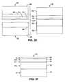
- a second wafer 60(FIG. 3D) is formed.
- formation of the second wafer 60starts in step 62 where a second silicon substrate 64 is processed such that a strained silicon-germanium layer 66 is formed thereon.
- the silicon-germanium layer 66is about 200 ⁇ to about 400 ⁇ thick and, at the conclusion of the method 50 , will become the silicon-germanium layer 22 (FIG. 1 ).
- the silicon-germanium layer 66is formed by depositing silicon-germanium using selective or nonselective epitaxy. Alternatively, germanium can be implanted into an upper region of the silicon substrate 64 .
- a silicon layer 70is formed on the silicon-germanium layer 66 .
- the silicon layer 70has a thickness of about 200 ⁇ to about 400 ⁇ .
- the silicon layer 70can be formed using, for example, selective or nonselective epitaxy.
- the silicon layer 70is processed such that an oxide layer 74 is formed in an upper region of the silicon layer 70 .
- the oxide layer 74is about 100 ⁇ to about 200 ⁇ thick.
- the remaining silicon of the silicon layer 70is about 100 ⁇ to about 200 ⁇ thick and, at the conclusion of the method 50 , will become the lower silicon layer 24 (FIG. 1 ).
- the oxide layer 74can be formed using a number of known techniques, such as thermal oxidation or by implanting oxygen ions into an upper region of the silicon layer 70 . Should the oxide layer 74 be formed using thermal oxidation, the silicon layer 70 is subjected to a thermal cycle having a temperature of about 1000° C. to about 1200° C. for about two seconds to about one minute in a pure (i.e., 100%), or nearly pure, oxygen atmosphere. The oxygen in the atmosphere reacts with the silicon of the silicon layer 70 to form silicon dioxide (SiO 2 ), resulting in the oxide layer 74 .
- the second wafer 60has a silicon substrate 64 with a silicon-germanium layer 66 disposed thereon. Disposed on the silicon-germanium layer 66 is a silicon layer 70 having an oxide layer 74 disposed thereon.
- step 76 and as illustrated in FIG. 3Ethe first wafer 52 and the second wafer 60 are combined using a wafer bonding technique to form a third wafer 78 .
- Wafer bondingis well known in the art and, therefore, will only be briefly discussed herein. Briefly, in a nitrogen (N 2 ) atmosphere, the second wafer 60 is inverted and placed in contact with the first wafer 54 such that the oxide layer 74 is contacting the oxide layer 58 . The oxide layers 58 and 74 bond to form an oxide layer 80 which, at the conclusion of the method 50 , will become the BOX layer 16 (FIG. 1 ).
- the third wafer 78is processed to reduce the thickness of the second substrate 64 to a thickness of about 100 ⁇ to about 200 ⁇ .
- the remaining silicon of the second substrate 64becomes the upper layer of silicon 20 .
- the silicon of the second substrate 64can be removed by controlled mechanical removal using, for example, mechanical polishing followed by a chemical-mechanical polish (CMP).
- CMPchemical-mechanical polish
- an embedded weak zonecan be formed in the second substrate 64 along which the second substrate is broken and a top portion removed.
- the remaining silicon materialcan be polished to the desired thickness of the upper silicon layer 20 .
- the wafer 12results. More specifically, the wafer 12 is comprised of the active layer 14 which includes the upper silicon layer 20 disposed on the silicon-germanium layer 22 which is disposed on the lower layer of silicon 24 . The active layer 14 is disposed, on the BOX layer 16 , which, in turn, is disposed on the substrate 18 .
- active devicescan be fabricated in step 82 . These active devices can include, for example, MOSFETs such as the device 10 illustrated in FIG. 1 .
Landscapes
- Engineering & Computer Science (AREA)
- Physics & Mathematics (AREA)
- Condensed Matter Physics & Semiconductors (AREA)
- General Physics & Mathematics (AREA)
- Manufacturing & Machinery (AREA)
- Computer Hardware Design (AREA)
- Microelectronics & Electronic Packaging (AREA)
- Power Engineering (AREA)
- Thin Film Transistor (AREA)
- Element Separation (AREA)
Abstract
Description
Claims (13)
Priority Applications (1)
| Application Number | Priority Date | Filing Date | Title |
|---|---|---|---|
| US10/116,791US6765227B1 (en) | 2001-02-26 | 2002-04-04 | Semiconductor-on-insulator (SOI) wafer having a Si/SiGe/Si active layer and method of fabrication using wafer bonding |
Applications Claiming Priority (2)
| Application Number | Priority Date | Filing Date | Title |
|---|---|---|---|
| US09/794,884US6410371B1 (en) | 2001-02-26 | 2001-02-26 | Method of fabrication of semiconductor-on-insulator (SOI) wafer having a Si/SiGe/Si active layer |
| US10/116,791US6765227B1 (en) | 2001-02-26 | 2002-04-04 | Semiconductor-on-insulator (SOI) wafer having a Si/SiGe/Si active layer and method of fabrication using wafer bonding |
Related Parent Applications (1)
| Application Number | Title | Priority Date | Filing Date |
|---|---|---|---|
| US09/794,884DivisionUS6410371B1 (en) | 2001-02-26 | 2001-02-26 | Method of fabrication of semiconductor-on-insulator (SOI) wafer having a Si/SiGe/Si active layer |
Publications (1)
| Publication Number | Publication Date |
|---|---|
| US6765227B1true US6765227B1 (en) | 2004-07-20 |
Family
ID=25163987
Family Applications (2)
| Application Number | Title | Priority Date | Filing Date |
|---|---|---|---|
| US09/794,884Expired - LifetimeUS6410371B1 (en) | 2001-02-26 | 2001-02-26 | Method of fabrication of semiconductor-on-insulator (SOI) wafer having a Si/SiGe/Si active layer |
| US10/116,791Expired - LifetimeUS6765227B1 (en) | 2001-02-26 | 2002-04-04 | Semiconductor-on-insulator (SOI) wafer having a Si/SiGe/Si active layer and method of fabrication using wafer bonding |
Family Applications Before (1)
| Application Number | Title | Priority Date | Filing Date |
|---|---|---|---|
| US09/794,884Expired - LifetimeUS6410371B1 (en) | 2001-02-26 | 2001-02-26 | Method of fabrication of semiconductor-on-insulator (SOI) wafer having a Si/SiGe/Si active layer |
Country Status (1)
| Country | Link |
|---|---|
| US (2) | US6410371B1 (en) |
Cited By (18)
| Publication number | Priority date | Publication date | Assignee | Title |
|---|---|---|---|---|
| US20040065925A1 (en)* | 2002-10-02 | 2004-04-08 | Arup Bhattacharyya | Semiconductor constructions comprising three-dimensional thin film transistor devices and resistors; and processes of forming stacked resistor constructions |
| US20040155317A1 (en)* | 2003-02-10 | 2004-08-12 | Arup Bhattacharyya | Transistor constructions and electronic devices |
| US20050090082A1 (en)* | 2003-10-28 | 2005-04-28 | Texas Instruments Incorporated | Method and system for improving performance of MOSFETs |
| US20050189610A1 (en)* | 2004-02-27 | 2005-09-01 | Koji Usuda | Semiconductor device and method of manufacturing the same |
| US20060189109A1 (en)* | 2001-03-02 | 2006-08-24 | Amberwave Systems | Methods of fabricating contact regions for FET incorporating SiGe |
| US20060194387A1 (en)* | 2005-02-25 | 2006-08-31 | Chih-Hao Wang | High performance transistors with SiGe strain |
| US7170084B1 (en)* | 2002-09-30 | 2007-01-30 | Advanced Micro Devices, Inc. | Strained silicon MOSFET having improved source/drain extension dopant diffusion resistance and method for its fabrication |
| US20080067544A1 (en)* | 2004-09-30 | 2008-03-20 | Siegfried Mantl | Method for Producing a Strained Layer on a Substrate and Layered Structure |
| US20080315253A1 (en)* | 2006-02-13 | 2008-12-25 | Wisconsin Alumni Research Foundation | Front and backside processed thin film electronic devices |
| US20090001417A1 (en)* | 2007-06-29 | 2009-01-01 | International Business Machines Corporation | Structures and methods of forming sige and sigec buried layer for soi/sige technology |
| US20090001414A1 (en)* | 2007-06-29 | 2009-01-01 | Xuefeng Liu | Structures and methods of forming sige and sigec buried layer for soi/sige technology |
| US7501351B2 (en)* | 2001-03-02 | 2009-03-10 | Amberwave Systems Corporation | Relaxed SiGe platform for high speed CMOS electronics and high speed analog circuits |
| US7960218B2 (en) | 2006-09-08 | 2011-06-14 | Wisconsin Alumni Research Foundation | Method for fabricating high-speed thin-film transistors |
| US8124470B1 (en) | 2010-09-29 | 2012-02-28 | International Business Machines Corporation | Strained thin body semiconductor-on-insulator substrate and device |
| US9799756B1 (en)* | 2016-08-05 | 2017-10-24 | International Business Machines Corporation | Germanium lateral bipolar transistor with silicon passivation |
| US20170317103A1 (en)* | 2016-04-28 | 2017-11-02 | Globalfoundries Singapore Pte. Ltd. | Integrated circuits with selectively strained device regions and methods for fabricating same |
| US11177250B2 (en) | 2019-09-17 | 2021-11-16 | Tokyo Electron Limited | Method for fabrication of high density logic and memory for advanced circuit architecture |
| US11673798B2 (en) | 2020-10-29 | 2023-06-13 | International Business Machines Corporation | Microfluidic devices with electrodes formed as physically separated sections of microchannel side walls |
Families Citing this family (56)
| Publication number | Priority date | Publication date | Assignee | Title |
|---|---|---|---|---|
| US7227176B2 (en) | 1998-04-10 | 2007-06-05 | Massachusetts Institute Of Technology | Etch stop layer system |
| US6754104B2 (en)* | 2000-06-22 | 2004-06-22 | Progressant Technologies, Inc. | Insulated-gate field-effect transistor integrated with negative differential resistance (NDR) FET |
| US6573126B2 (en) | 2000-08-16 | 2003-06-03 | Massachusetts Institute Of Technology | Process for producing semiconductor article using graded epitaxial growth |
| WO2002082514A1 (en) | 2001-04-04 | 2002-10-17 | Massachusetts Institute Of Technology | A method for semiconductor device fabrication |
| US6717213B2 (en)* | 2001-06-29 | 2004-04-06 | Intel Corporation | Creation of high mobility channels in thin-body SOI devices |
| JP3647777B2 (en)* | 2001-07-06 | 2005-05-18 | 株式会社東芝 | Method of manufacturing field effect transistor and integrated circuit element |
| JP2003205336A (en)* | 2002-01-08 | 2003-07-22 | Tori Techno:Kk | High strength stainless steel bolt and manufacturing method therefor |
| US6649492B2 (en)* | 2002-02-11 | 2003-11-18 | International Business Machines Corporation | Strained Si based layer made by UHV-CVD, and devices therein |
| WO2003079415A2 (en)* | 2002-03-14 | 2003-09-25 | Amberwave Systems Corporation | Methods for fabricating strained layers on semiconductor substrates |
| US7615829B2 (en) | 2002-06-07 | 2009-11-10 | Amberwave Systems Corporation | Elevated source and drain elements for strained-channel heterojuntion field-effect transistors |
| US6995430B2 (en) | 2002-06-07 | 2006-02-07 | Amberwave Systems Corporation | Strained-semiconductor-on-insulator device structures |
| US7335545B2 (en) | 2002-06-07 | 2008-02-26 | Amberwave Systems Corporation | Control of strain in device layers by prevention of relaxation |
| US20030227057A1 (en) | 2002-06-07 | 2003-12-11 | Lochtefeld Anthony J. | Strained-semiconductor-on-insulator device structures |
| US7307273B2 (en) | 2002-06-07 | 2007-12-11 | Amberwave Systems Corporation | Control of strain in device layers by selective relaxation |
| US7074623B2 (en) | 2002-06-07 | 2006-07-11 | Amberwave Systems Corporation | Methods of forming strained-semiconductor-on-insulator finFET device structures |
| US6946371B2 (en) | 2002-06-10 | 2005-09-20 | Amberwave Systems Corporation | Methods of fabricating semiconductor structures having epitaxially grown source and drain elements |
| US6982474B2 (en) | 2002-06-25 | 2006-01-03 | Amberwave Systems Corporation | Reacted conductive gate electrodes |
| US6743662B2 (en)* | 2002-07-01 | 2004-06-01 | Honeywell International, Inc. | Silicon-on-insulator wafer for RF integrated circuit |
| US6953736B2 (en)* | 2002-07-09 | 2005-10-11 | S.O.I.Tec Silicon On Insulator Technologies S.A. | Process for transferring a layer of strained semiconductor material |
| US7018910B2 (en) | 2002-07-09 | 2006-03-28 | S.O.I.Tec Silicon On Insulator Technologies S.A. | Transfer of a thin layer from a wafer comprising a buffer layer |
| FR2842349B1 (en)* | 2002-07-09 | 2005-02-18 | TRANSFERRING A THIN LAYER FROM A PLATE COMPRISING A BUFFER LAYER | |
| US6878610B1 (en)* | 2002-08-27 | 2005-04-12 | Taiwan Semiconductor Manufacturing Company, Ltd. | Relaxed silicon germanium substrate with low defect density |
| US6911379B2 (en)* | 2003-03-05 | 2005-06-28 | Taiwan Semiconductor Manufacturing Company, Ltd. | Method of forming strained silicon on insulator substrate |
| WO2004081982A2 (en) | 2003-03-07 | 2004-09-23 | Amberwave Systems Corporation | Shallow trench isolation process |
| US6949451B2 (en)* | 2003-03-10 | 2005-09-27 | Taiwan Semiconductor Manufacturing Company, Ltd. | SOI chip with recess-resistant buried insulator and method of manufacturing the same |
| US6902962B2 (en)* | 2003-04-04 | 2005-06-07 | Taiwan Semiconductor Manufacturing Company, Ltd. | Silicon-on-insulator chip with multiple crystal orientations |
| US6864149B2 (en)* | 2003-05-09 | 2005-03-08 | Taiwan Semiconductor Manufacturing Company | SOI chip with mesa isolation and recess resistant regions |
| US7183611B2 (en)* | 2003-06-03 | 2007-02-27 | Micron Technology, Inc. | SRAM constructions, and electronic systems comprising SRAM constructions |
| US7586116B2 (en)* | 2003-06-26 | 2009-09-08 | Mears Technologies, Inc. | Semiconductor device having a semiconductor-on-insulator configuration and a superlattice |
| US6909151B2 (en)* | 2003-06-27 | 2005-06-21 | Intel Corporation | Nonplanar device with stress incorporation layer and method of fabrication |
| CN100397575C (en)* | 2003-10-30 | 2008-06-25 | 台湾积体电路制造股份有限公司 | Strained multilayer structure and method for manufacturing field effect transistor with strained layer |
| CN100397574C (en)* | 2003-10-30 | 2008-06-25 | 台湾积体电路制造股份有限公司 | Strained multilayer structure and method for manufacturing field effect transistor with strained layer |
| US6902965B2 (en)* | 2003-10-31 | 2005-06-07 | Taiwan Semiconductor Manufacturing Company, Ltd. | Strained silicon structure |
| US7247534B2 (en) | 2003-11-19 | 2007-07-24 | International Business Machines Corporation | Silicon device on Si:C-OI and SGOI and method of manufacture |
| CN100459042C (en)* | 2003-12-16 | 2009-02-04 | Nxp股份有限公司 | Method for forming a strained Si-channel in a MOFSET structure |
| FR2864336B1 (en)* | 2003-12-23 | 2006-04-28 | Commissariat Energie Atomique | METHOD FOR SEALING TWO PLATES WITH FORMATION OF AN OHMIC CONTACT BETWEEN THEM |
| US7042009B2 (en) | 2004-06-30 | 2006-05-09 | Intel Corporation | High mobility tri-gate devices and methods of fabrication |
| US7115955B2 (en)* | 2004-07-30 | 2006-10-03 | International Business Machines Corporation | Semiconductor device having a strained raised source/drain |
| US7348284B2 (en) | 2004-08-10 | 2008-03-25 | Intel Corporation | Non-planar pMOS structure with a strained channel region and an integrated strained CMOS flow |
| US7422946B2 (en) | 2004-09-29 | 2008-09-09 | Intel Corporation | Independently accessed double-gate and tri-gate transistors in same process flow |
| US7361958B2 (en)* | 2004-09-30 | 2008-04-22 | Intel Corporation | Nonplanar transistors with metal gate electrodes |
| US20060086977A1 (en) | 2004-10-25 | 2006-04-27 | Uday Shah | Nonplanar device with thinned lower body portion and method of fabrication |
| US7393733B2 (en) | 2004-12-01 | 2008-07-01 | Amberwave Systems Corporation | Methods of forming hybrid fin field-effect transistor structures |
| US7288940B2 (en)* | 2004-12-06 | 2007-10-30 | Analog Devices, Inc. | Galvanically isolated signal conditioning system |
| US7229901B2 (en)* | 2004-12-16 | 2007-06-12 | Wisconsin Alumni Research Foundation | Fabrication of strained heterojunction structures |
| US7518196B2 (en) | 2005-02-23 | 2009-04-14 | Intel Corporation | Field effect transistor with narrow bandgap source and drain regions and method of fabrication |
| US7402875B2 (en) | 2005-08-17 | 2008-07-22 | Intel Corporation | Lateral undercut of metal gate in SOI device |
| US8420505B2 (en)* | 2006-03-25 | 2013-04-16 | International Rectifier Corporation | Process for manufacture of thin wafer |
| JP2009536464A (en)* | 2006-05-05 | 2009-10-08 | メアーズ テクノロジーズ, インコーポレイテッド | Semiconductor device having superlattice arrangement with semiconductor present on insulator and related method |
| US8013342B2 (en)* | 2007-11-14 | 2011-09-06 | International Business Machines Corporation | Double-sided integrated circuit chips |
| US7670927B2 (en)* | 2006-05-16 | 2010-03-02 | International Business Machines Corporation | Double-sided integrated circuit chips |
| US7777290B2 (en)* | 2006-06-13 | 2010-08-17 | Wisconsin Alumni Research Foundation | PIN diodes for photodetection and high-speed, high-resolution image sensing |
| US8362566B2 (en) | 2008-06-23 | 2013-01-29 | Intel Corporation | Stress in trigate devices using complimentary gate fill materials |
| FR2974245B1 (en)* | 2011-04-14 | 2014-01-31 | Soitec Silicon On Insulator | QUANTUM WELL THERMOELECTRIC COMPONENT FOR USE IN A THERMOELECTRIC DEVICE |
| US9105689B1 (en)* | 2014-03-24 | 2015-08-11 | Silanna Semiconductor U.S.A., Inc. | Bonded semiconductor structure with SiGeC layer as etch stop |
| US20170062569A1 (en)* | 2014-06-13 | 2017-03-02 | Intel Corporation | Surface encapsulation for wafer bonding |
Citations (29)
| Publication number | Priority date | Publication date | Assignee | Title |
|---|---|---|---|---|
| JPH05183154A (en)* | 1992-01-06 | 1993-07-23 | Toshiba Corp | Semiconductor device and manufacturing method thereof |
| US5234535A (en) | 1992-12-10 | 1993-08-10 | International Business Machines Corporation | Method of producing a thin silicon-on-insulator layer |
| US5357119A (en)* | 1993-02-19 | 1994-10-18 | Board Of Regents Of The University Of California | Field effect devices having short period superlattice structures using Si and Ge |
| US5438015A (en) | 1994-05-11 | 1995-08-01 | United Microelectronics Corp. | Silicon-on-insulator technique with buried gap |
| US5461243A (en) | 1993-10-29 | 1995-10-24 | International Business Machines Corporation | Substrate for tensilely strained semiconductor |
| US5461250A (en)* | 1992-08-10 | 1995-10-24 | International Business Machines Corporation | SiGe thin film or SOI MOSFET and method for making the same |
| US5583059A (en) | 1994-06-01 | 1996-12-10 | International Business Machines Corporation | Fabrication of vertical SiGe base HBT with lateral collector contact on thin SOI |
| US5683934A (en) | 1994-09-26 | 1997-11-04 | Motorola, Inc. | Enhanced mobility MOSFET device and method |
| US5686735A (en)* | 1994-06-13 | 1997-11-11 | Samsung Electronics Co., Ltd. | Silicon-on-insulator (SOI) transistor |
| US5714777A (en) | 1997-02-19 | 1998-02-03 | International Business Machines Corporation | Si/SiGe vertical junction field effect transistor |
| JPH1093076A (en)* | 1996-09-18 | 1998-04-10 | Oki Electric Ind Co Ltd | Mos field-effect transistor and manufacturing method thereof |
| US5821577A (en)* | 1991-01-10 | 1998-10-13 | International Business Machines Corporation | Graded channel field effect transistor |
| US5847419A (en) | 1996-09-17 | 1998-12-08 | Kabushiki Kaisha Toshiba | Si-SiGe semiconductor device and method of fabricating the same |
| US5849627A (en) | 1990-02-07 | 1998-12-15 | Harris Corporation | Bonded wafer processing with oxidative bonding |
| US5906951A (en) | 1997-04-30 | 1999-05-25 | International Business Machines Corporation | Strained Si/SiGe layers on insulator |
| US5963817A (en) | 1997-10-16 | 1999-10-05 | International Business Machines Corporation | Bulk and strained silicon on insulator using local selective oxidation |
| US5986287A (en)* | 1995-09-08 | 1999-11-16 | Max-Planck-Gesellschaft Zur Foerderung Der Wissenschaften E. V. | Semiconductor structure for a transistor |
| US5998807A (en)* | 1996-09-27 | 1999-12-07 | Siemens Aktiengesellschaft | Integrated CMOS circuit arrangement and method for the manufacture thereof |
| US6008077A (en)* | 1997-08-22 | 1999-12-28 | Mitsubishi Denki Kabushiki Kaisha | Method for fabricating semiconductor device |
| US6111267A (en)* | 1997-05-13 | 2000-08-29 | Siemens Aktiengesellschaft | CMOS integrated circuit including forming doped wells, a layer of intrinsic silicon, a stressed silicon germanium layer where germanium is between 25 and 50%, and another intrinsic silicon layer |
| US6153495A (en) | 1998-03-09 | 2000-11-28 | Intersil Corporation | Advanced methods for making semiconductor devices by low temperature direct bonding |
| JP2001217433A (en)* | 2000-01-07 | 2001-08-10 | Samsung Electronics Co Ltd | CMOS integrated circuit device and substrate having buried silicon germanium layer and method of manufacturing the same |
| US6287903B1 (en)* | 1997-12-24 | 2001-09-11 | Texas Instruments Incorporated | Structure and method for a large-permittivity dielectric using a germanium layer |
| US20020008289A1 (en)* | 2000-07-24 | 2002-01-24 | Junichi Murota | Mosfet with strained channel layer |
| US6353245B1 (en)* | 1998-04-09 | 2002-03-05 | Texas Instruments Incorporated | Body-tied-to-source partially depleted SOI MOSFET |
| US20020052084A1 (en)* | 2000-05-26 | 2002-05-02 | Fitzgerald Eugene A. | Buried channel strained silicon FET using a supply layer created through ion implantation |
| US6437375B1 (en)* | 2000-06-05 | 2002-08-20 | Micron Technology, Inc. | PD-SOI substrate with suppressed floating body effect and method for its fabrication |
| US6476445B1 (en)* | 1999-04-30 | 2002-11-05 | International Business Machines Corporation | Method and structures for dual depth oxygen layers in silicon-on-insulator processes |
| US6633066B1 (en)* | 2000-01-07 | 2003-10-14 | Samsung Electronics Co., Ltd. | CMOS integrated circuit devices and substrates having unstrained silicon active layers |
- 2001
- 2001-02-26USUS09/794,884patent/US6410371B1/ennot_activeExpired - Lifetime
- 2002
- 2002-04-04USUS10/116,791patent/US6765227B1/ennot_activeExpired - Lifetime
Patent Citations (30)
| Publication number | Priority date | Publication date | Assignee | Title |
|---|---|---|---|---|
| US5849627A (en) | 1990-02-07 | 1998-12-15 | Harris Corporation | Bonded wafer processing with oxidative bonding |
| US5821577A (en)* | 1991-01-10 | 1998-10-13 | International Business Machines Corporation | Graded channel field effect transistor |
| JPH05183154A (en)* | 1992-01-06 | 1993-07-23 | Toshiba Corp | Semiconductor device and manufacturing method thereof |
| US5461250A (en)* | 1992-08-10 | 1995-10-24 | International Business Machines Corporation | SiGe thin film or SOI MOSFET and method for making the same |
| US5234535A (en) | 1992-12-10 | 1993-08-10 | International Business Machines Corporation | Method of producing a thin silicon-on-insulator layer |
| US5357119A (en)* | 1993-02-19 | 1994-10-18 | Board Of Regents Of The University Of California | Field effect devices having short period superlattice structures using Si and Ge |
| US5461243A (en) | 1993-10-29 | 1995-10-24 | International Business Machines Corporation | Substrate for tensilely strained semiconductor |
| US5438015A (en) | 1994-05-11 | 1995-08-01 | United Microelectronics Corp. | Silicon-on-insulator technique with buried gap |
| US5583059A (en) | 1994-06-01 | 1996-12-10 | International Business Machines Corporation | Fabrication of vertical SiGe base HBT with lateral collector contact on thin SOI |
| US5686735A (en)* | 1994-06-13 | 1997-11-11 | Samsung Electronics Co., Ltd. | Silicon-on-insulator (SOI) transistor |
| US5683934A (en) | 1994-09-26 | 1997-11-04 | Motorola, Inc. | Enhanced mobility MOSFET device and method |
| US5986287A (en)* | 1995-09-08 | 1999-11-16 | Max-Planck-Gesellschaft Zur Foerderung Der Wissenschaften E. V. | Semiconductor structure for a transistor |
| US5847419A (en) | 1996-09-17 | 1998-12-08 | Kabushiki Kaisha Toshiba | Si-SiGe semiconductor device and method of fabricating the same |
| JPH1093076A (en)* | 1996-09-18 | 1998-04-10 | Oki Electric Ind Co Ltd | Mos field-effect transistor and manufacturing method thereof |
| US5998807A (en)* | 1996-09-27 | 1999-12-07 | Siemens Aktiengesellschaft | Integrated CMOS circuit arrangement and method for the manufacture thereof |
| US5714777A (en) | 1997-02-19 | 1998-02-03 | International Business Machines Corporation | Si/SiGe vertical junction field effect transistor |
| US5906951A (en) | 1997-04-30 | 1999-05-25 | International Business Machines Corporation | Strained Si/SiGe layers on insulator |
| US6059895A (en) | 1997-04-30 | 2000-05-09 | International Business Machines Corporation | Strained Si/SiGe layers on insulator |
| US6111267A (en)* | 1997-05-13 | 2000-08-29 | Siemens Aktiengesellschaft | CMOS integrated circuit including forming doped wells, a layer of intrinsic silicon, a stressed silicon germanium layer where germanium is between 25 and 50%, and another intrinsic silicon layer |
| US6008077A (en)* | 1997-08-22 | 1999-12-28 | Mitsubishi Denki Kabushiki Kaisha | Method for fabricating semiconductor device |
| US5963817A (en) | 1997-10-16 | 1999-10-05 | International Business Machines Corporation | Bulk and strained silicon on insulator using local selective oxidation |
| US6287903B1 (en)* | 1997-12-24 | 2001-09-11 | Texas Instruments Incorporated | Structure and method for a large-permittivity dielectric using a germanium layer |
| US6153495A (en) | 1998-03-09 | 2000-11-28 | Intersil Corporation | Advanced methods for making semiconductor devices by low temperature direct bonding |
| US6353245B1 (en)* | 1998-04-09 | 2002-03-05 | Texas Instruments Incorporated | Body-tied-to-source partially depleted SOI MOSFET |
| US6476445B1 (en)* | 1999-04-30 | 2002-11-05 | International Business Machines Corporation | Method and structures for dual depth oxygen layers in silicon-on-insulator processes |
| JP2001217433A (en)* | 2000-01-07 | 2001-08-10 | Samsung Electronics Co Ltd | CMOS integrated circuit device and substrate having buried silicon germanium layer and method of manufacturing the same |
| US6633066B1 (en)* | 2000-01-07 | 2003-10-14 | Samsung Electronics Co., Ltd. | CMOS integrated circuit devices and substrates having unstrained silicon active layers |
| US20020052084A1 (en)* | 2000-05-26 | 2002-05-02 | Fitzgerald Eugene A. | Buried channel strained silicon FET using a supply layer created through ion implantation |
| US6437375B1 (en)* | 2000-06-05 | 2002-08-20 | Micron Technology, Inc. | PD-SOI substrate with suppressed floating body effect and method for its fabrication |
| US20020008289A1 (en)* | 2000-07-24 | 2002-01-24 | Junichi Murota | Mosfet with strained channel layer |
Non-Patent Citations (1)
| Title |
|---|
| Quinones et al, "Design, Fabrication, and Analysis of SiGeC Hetrojunction of PMOSFETs" IEEE trans. on electronic devices vol. 47, No. 9, Sep. 2000.* |
Cited By (43)
| Publication number | Priority date | Publication date | Assignee | Title |
|---|---|---|---|---|
| US7501351B2 (en)* | 2001-03-02 | 2009-03-10 | Amberwave Systems Corporation | Relaxed SiGe platform for high speed CMOS electronics and high speed analog circuits |
| US8822282B2 (en) | 2001-03-02 | 2014-09-02 | Taiwan Semiconductor Manufacturing Company, Ltd. | Methods of fabricating contact regions for FET incorporating SiGe |
| US20060189109A1 (en)* | 2001-03-02 | 2006-08-24 | Amberwave Systems | Methods of fabricating contact regions for FET incorporating SiGe |
| US7170084B1 (en)* | 2002-09-30 | 2007-01-30 | Advanced Micro Devices, Inc. | Strained silicon MOSFET having improved source/drain extension dopant diffusion resistance and method for its fabrication |
| US6873015B2 (en)* | 2002-10-02 | 2005-03-29 | Micron Technology, Inc. | Semiconductor constructions comprising three-dimensional thin film transistor devices and resistors |
| US7148544B2 (en) | 2002-10-02 | 2006-12-12 | Micron Technology, Inc. | Semiconductor-on-insulator constructions |
| US20050056894A1 (en)* | 2002-10-02 | 2005-03-17 | Arup Bhattacharyya | Semiconductor-on-insulator constructions |
| US20040065925A1 (en)* | 2002-10-02 | 2004-04-08 | Arup Bhattacharyya | Semiconductor constructions comprising three-dimensional thin film transistor devices and resistors; and processes of forming stacked resistor constructions |
| US7221026B2 (en) | 2002-10-02 | 2007-05-22 | Micron Technology, Inc. | Computer systems containing resistors which include doped silicon/germanium |
| US20050062045A1 (en)* | 2002-10-02 | 2005-03-24 | Arup Bhattacharyya | Processes of forming stacked resistor constructions |
| US7190028B2 (en)* | 2002-10-02 | 2007-03-13 | Micron Technology, Inc. | Semiconductor-on-insulator constructions |
| US7151037B2 (en) | 2002-10-02 | 2006-12-19 | Micron Technology, Inc. | Processes of forming stacked resistor constructions |
| US20050056911A1 (en)* | 2002-10-02 | 2005-03-17 | Arup Bhattacharyya | Semiconductor-on-insulator constructions |
| US20050045991A1 (en)* | 2002-10-02 | 2005-03-03 | Arup Bhattacharyya | Computer systems containing resistors which include doped silicon/germanium |
| US20050247982A1 (en)* | 2003-02-10 | 2005-11-10 | Arup Bhattacharyya | Transistor constructions and electronic devices |
| US7115948B2 (en)* | 2003-02-10 | 2006-10-03 | Micron Technology, Inc. | Transistor constructions and electronic devices |
| US20060125010A1 (en)* | 2003-02-10 | 2006-06-15 | Arup Bhattacharyya | Methods of forming transistor constructions |
| US20040155317A1 (en)* | 2003-02-10 | 2004-08-12 | Arup Bhattacharyya | Transistor constructions and electronic devices |
| US7042052B2 (en)* | 2003-02-10 | 2006-05-09 | Micron Technology, Inc. | Transistor constructions and electronic devices |
| US7291519B2 (en) | 2003-02-10 | 2007-11-06 | Micron Technology, Inc. | Methods of forming transistor constructions |
| US20050090082A1 (en)* | 2003-10-28 | 2005-04-28 | Texas Instruments Incorporated | Method and system for improving performance of MOSFETs |
| US20050189610A1 (en)* | 2004-02-27 | 2005-09-01 | Koji Usuda | Semiconductor device and method of manufacturing the same |
| US20080067544A1 (en)* | 2004-09-30 | 2008-03-20 | Siegfried Mantl | Method for Producing a Strained Layer on a Substrate and Layered Structure |
| US8048220B2 (en)* | 2004-09-30 | 2011-11-01 | Forschungszentrum Julich Gmbh | Method for producing a strained layer on a substrate and layered structure |
| US7268362B2 (en)* | 2005-02-25 | 2007-09-11 | Taiwan Semiconductor Manufacturing Company, Ltd. | High performance transistors with SiGe strain |
| US20060194387A1 (en)* | 2005-02-25 | 2006-08-31 | Chih-Hao Wang | High performance transistors with SiGe strain |
| US20080315253A1 (en)* | 2006-02-13 | 2008-12-25 | Wisconsin Alumni Research Foundation | Front and backside processed thin film electronic devices |
| WO2007094824A3 (en)* | 2006-02-13 | 2009-04-23 | Wisconsin Alumni Res Found | Method for double-sided processing of thin film transistors |
| US7812353B2 (en) | 2006-02-13 | 2010-10-12 | Wisconsin Alumni Research Foundation | Front and backside processed thin film electronic devices |
| US7960218B2 (en) | 2006-09-08 | 2011-06-14 | Wisconsin Alumni Research Foundation | Method for fabricating high-speed thin-film transistors |
| US9087925B2 (en) | 2007-06-29 | 2015-07-21 | International Business Machines Corporation | Si and SiGeC on a buried oxide layer on a substrate |
| US20110227130A1 (en)* | 2007-06-29 | 2011-09-22 | International Business Machines Corporation | Structures and methods of forming sige and sigec buried layer for soi/sige technology |
| US7989306B2 (en) | 2007-06-29 | 2011-08-02 | International Business Machines Corporation | Method of forming alternating regions of Si and SiGe or SiGeC on a buried oxide layer on a substrate |
| US8138579B2 (en) | 2007-06-29 | 2012-03-20 | International Business Machines Corporation | Structures and methods of forming SiGe and SiGeC buried layer for SOI/SiGe technology |
| US20090001417A1 (en)* | 2007-06-29 | 2009-01-01 | International Business Machines Corporation | Structures and methods of forming sige and sigec buried layer for soi/sige technology |
| US20090001414A1 (en)* | 2007-06-29 | 2009-01-01 | Xuefeng Liu | Structures and methods of forming sige and sigec buried layer for soi/sige technology |
| US8124470B1 (en) | 2010-09-29 | 2012-02-28 | International Business Machines Corporation | Strained thin body semiconductor-on-insulator substrate and device |
| US8368143B2 (en) | 2010-09-29 | 2013-02-05 | International Business Machines Corporation | Strained thin body semiconductor-on-insulator substrate and device |
| US20170317103A1 (en)* | 2016-04-28 | 2017-11-02 | Globalfoundries Singapore Pte. Ltd. | Integrated circuits with selectively strained device regions and methods for fabricating same |
| US10529738B2 (en)* | 2016-04-28 | 2020-01-07 | Globalfoundries Singapore Pte. Ltd. | Integrated circuits with selectively strained device regions and methods for fabricating same |
| US9799756B1 (en)* | 2016-08-05 | 2017-10-24 | International Business Machines Corporation | Germanium lateral bipolar transistor with silicon passivation |
| US11177250B2 (en) | 2019-09-17 | 2021-11-16 | Tokyo Electron Limited | Method for fabrication of high density logic and memory for advanced circuit architecture |
| US11673798B2 (en) | 2020-10-29 | 2023-06-13 | International Business Machines Corporation | Microfluidic devices with electrodes formed as physically separated sections of microchannel side walls |
Also Published As
| Publication number | Publication date |
|---|---|
| US6410371B1 (en) | 2002-06-25 |
Similar Documents
| Publication | Publication Date | Title |
|---|---|---|
| US6765227B1 (en) | Semiconductor-on-insulator (SOI) wafer having a Si/SiGe/Si active layer and method of fabrication using wafer bonding | |
| US6787852B1 (en) | Semiconductor-on-insulator (SOI) device having source/drain silicon-germanium regions | |
| US6380590B1 (en) | SOI chip having multiple threshold voltage MOSFETs by using multiple channel materials and method of fabricating same | |
| US8575699B2 (en) | Thin box metal backgate extremely thin SOI device | |
| US7767546B1 (en) | Low cost fabrication of double box back gate silicon-on-insulator wafers with built-in shallow trench isolation in back gate layer | |
| KR0176202B1 (en) | S.O.I transistor and its manufacturing method | |
| US8587063B2 (en) | Hybrid double box back gate silicon-on-insulator wafers with enhanced mobility channels | |
| US7364958B2 (en) | CMOS on hybrid substrate with different crystal orientations using silicon-to-silicon direct wafer bonding | |
| US7915100B2 (en) | Hybrid orientation CMOS with partial insulation process | |
| US6680240B1 (en) | Silicon-on-insulator device with strained device film and method for making the same with partial replacement of isolation oxide | |
| US8877606B2 (en) | Low cost fabrication of double box back gate silicon-on-insulator wafers with subsequent self aligned shallow trench isolation | |
| US9355887B2 (en) | Dual trench isolation for CMOS with hybrid orientations | |
| US4951102A (en) | Trench gate VCMOS | |
| US7892901B2 (en) | Strained silicon-on-insulator transistors with mesa isolation | |
| US20050026390A1 (en) | Shallow trench filled with two or more dielectrics for isolation and coupling or for stress control | |
| US6787423B1 (en) | Strained-silicon semiconductor device | |
| US5032529A (en) | Trench gate VCMOS method of manufacture | |
| US20100176495A1 (en) | Low cost fabrication of double box back gate silicon-on-insulator wafers | |
| US6506638B1 (en) | Vertical double gate transistor structure | |
| JPH11340465A (en) | SOI semiconductor device and manufacturing method thereof | |
| US6724049B2 (en) | SOI semiconductor device with insulating film having different properties relative to the buried insulating film | |
| US6501135B1 (en) | Germanium-on-insulator (GOI) device | |
| US6809380B2 (en) | Semiconductor device formed on an SOI structure with a stress-relief layer | |
| US20010053569A1 (en) | Process for fabricating a MOS transistor having two gates, one of which is buried and corresponding transistor | |
| JP2005136410A (en) | Cmos on hybrid substrate with different crystal orientations formed by employing silicon-to-silicon direct wafer bonding |
Legal Events
| Date | Code | Title | Description |
|---|---|---|---|
| FEPP | Fee payment procedure | Free format text:PAYOR NUMBER ASSIGNED (ORIGINAL EVENT CODE: ASPN); ENTITY STATUS OF PATENT OWNER: LARGE ENTITY | |
| STCF | Information on status: patent grant | Free format text:PATENTED CASE | |
| CC | Certificate of correction | ||
| FPAY | Fee payment | Year of fee payment:4 | |
| AS | Assignment | Owner name:GLOBALFOUNDRIES INC., CAYMAN ISLANDS Free format text:AFFIRMATION OF PATENT ASSIGNMENT;ASSIGNOR:ADVANCED MICRO DEVICES, INC.;REEL/FRAME:023119/0083 Effective date:20090630 | |
| FPAY | Fee payment | Year of fee payment:8 | |
| FPAY | Fee payment | Year of fee payment:12 | |
| AS | Assignment | Owner name:WILMINGTON TRUST, NATIONAL ASSOCIATION, DELAWARE Free format text:SECURITY AGREEMENT;ASSIGNOR:GLOBALFOUNDRIES INC.;REEL/FRAME:049490/0001 Effective date:20181127 | |
| AS | Assignment | Owner name:GLOBALFOUNDRIES U.S. INC., CALIFORNIA Free format text:ASSIGNMENT OF ASSIGNORS INTEREST;ASSIGNOR:GLOBALFOUNDRIES INC.;REEL/FRAME:054633/0001 Effective date:20201022 | |
| AS | Assignment | Owner name:GLOBALFOUNDRIES INC., CAYMAN ISLANDS Free format text:RELEASE BY SECURED PARTY;ASSIGNOR:WILMINGTON TRUST, NATIONAL ASSOCIATION;REEL/FRAME:054636/0001 Effective date:20201117 | |
| AS | Assignment | Owner name:GLOBALFOUNDRIES U.S. INC., NEW YORK Free format text:RELEASE BY SECURED PARTY;ASSIGNOR:WILMINGTON TRUST, NATIONAL ASSOCIATION;REEL/FRAME:056987/0001 Effective date:20201117 |