US6764808B2 - Self-aligned pattern formation using wavelenghts - Google Patents
Self-aligned pattern formation using wavelenghtsDownload PDFInfo
- Publication number
- US6764808B2 US6764808B2US10/083,914US8391402AUS6764808B2US 6764808 B2US6764808 B2US 6764808B2US 8391402 AUS8391402 AUS 8391402AUS 6764808 B2US6764808 B2US 6764808B2
- Authority
- US
- United States
- Prior art keywords
- radiation
- wavelength
- lithographic
- photoresist
- top portion
- Prior art date
- Legal status (The legal status is an assumption and is not a legal conclusion. Google has not performed a legal analysis and makes no representation as to the accuracy of the status listed.)
- Expired - Lifetime
Links
Images


Classifications
- G—PHYSICS
- G03—PHOTOGRAPHY; CINEMATOGRAPHY; ANALOGOUS TECHNIQUES USING WAVES OTHER THAN OPTICAL WAVES; ELECTROGRAPHY; HOLOGRAPHY
- G03F—PHOTOMECHANICAL PRODUCTION OF TEXTURED OR PATTERNED SURFACES, e.g. FOR PRINTING, FOR PROCESSING OF SEMICONDUCTOR DEVICES; MATERIALS THEREFOR; ORIGINALS THEREFOR; APPARATUS SPECIALLY ADAPTED THEREFOR
- G03F7/00—Photomechanical, e.g. photolithographic, production of textured or patterned surfaces, e.g. printing surfaces; Materials therefor, e.g. comprising photoresists; Apparatus specially adapted therefor
- G03F7/70—Microphotolithographic exposure; Apparatus therefor
- G03F7/70425—Imaging strategies, e.g. for increasing throughput or resolution, printing product fields larger than the image field or compensating lithography- or non-lithography errors, e.g. proximity correction, mix-and-match, stitching or double patterning
- G03F7/7045—Hybrid exposures, i.e. multiple exposures of the same area using different types of exposure apparatus, e.g. combining projection, proximity, direct write, interferometric, UV, x-ray or particle beam
- G—PHYSICS
- G03—PHOTOGRAPHY; CINEMATOGRAPHY; ANALOGOUS TECHNIQUES USING WAVES OTHER THAN OPTICAL WAVES; ELECTROGRAPHY; HOLOGRAPHY
- G03F—PHOTOMECHANICAL PRODUCTION OF TEXTURED OR PATTERNED SURFACES, e.g. FOR PRINTING, FOR PROCESSING OF SEMICONDUCTOR DEVICES; MATERIALS THEREFOR; ORIGINALS THEREFOR; APPARATUS SPECIALLY ADAPTED THEREFOR
- G03F7/00—Photomechanical, e.g. photolithographic, production of textured or patterned surfaces, e.g. printing surfaces; Materials therefor, e.g. comprising photoresists; Apparatus specially adapted therefor
- G03F7/004—Photosensitive materials
- G03F7/075—Silicon-containing compounds
- G03F7/0757—Macromolecular compounds containing Si-O, Si-C or Si-N bonds
- G—PHYSICS
- G03—PHOTOGRAPHY; CINEMATOGRAPHY; ANALOGOUS TECHNIQUES USING WAVES OTHER THAN OPTICAL WAVES; ELECTROGRAPHY; HOLOGRAPHY
- G03F—PHOTOMECHANICAL PRODUCTION OF TEXTURED OR PATTERNED SURFACES, e.g. FOR PRINTING, FOR PROCESSING OF SEMICONDUCTOR DEVICES; MATERIALS THEREFOR; ORIGINALS THEREFOR; APPARATUS SPECIALLY ADAPTED THEREFOR
- G03F7/00—Photomechanical, e.g. photolithographic, production of textured or patterned surfaces, e.g. printing surfaces; Materials therefor, e.g. comprising photoresists; Apparatus specially adapted therefor
- G03F7/004—Photosensitive materials
- G03F7/09—Photosensitive materials characterised by structural details, e.g. supports, auxiliary layers
- G03F7/095—Photosensitive materials characterised by structural details, e.g. supports, auxiliary layers having more than one photosensitive layer
- G—PHYSICS
- G03—PHOTOGRAPHY; CINEMATOGRAPHY; ANALOGOUS TECHNIQUES USING WAVES OTHER THAN OPTICAL WAVES; ELECTROGRAPHY; HOLOGRAPHY
- G03F—PHOTOMECHANICAL PRODUCTION OF TEXTURED OR PATTERNED SURFACES, e.g. FOR PRINTING, FOR PROCESSING OF SEMICONDUCTOR DEVICES; MATERIALS THEREFOR; ORIGINALS THEREFOR; APPARATUS SPECIALLY ADAPTED THEREFOR
- G03F7/00—Photomechanical, e.g. photolithographic, production of textured or patterned surfaces, e.g. printing surfaces; Materials therefor, e.g. comprising photoresists; Apparatus specially adapted therefor
- G03F7/20—Exposure; Apparatus therefor
- G03F7/2022—Multi-step exposure, e.g. hybrid; backside exposure; blanket exposure, e.g. for image reversal; edge exposure, e.g. for edge bead removal; corrective exposure
- H—ELECTRICITY
- H01—ELECTRIC ELEMENTS
- H01L—SEMICONDUCTOR DEVICES NOT COVERED BY CLASS H10
- H01L21/00—Processes or apparatus adapted for the manufacture or treatment of semiconductor or solid state devices or of parts thereof
- H01L21/02—Manufacture or treatment of semiconductor devices or of parts thereof
- H01L21/027—Making masks on semiconductor bodies for further photolithographic processing not provided for in group H01L21/18 or H01L21/34
- H01L21/0271—Making masks on semiconductor bodies for further photolithographic processing not provided for in group H01L21/18 or H01L21/34 comprising organic layers
- H01L21/0273—Making masks on semiconductor bodies for further photolithographic processing not provided for in group H01L21/18 or H01L21/34 comprising organic layers characterised by the treatment of photoresist layers
- H01L21/0274—Photolithographic processes
Definitions
- the present inventionrelates generally to self-aligned pattern formation. More particularly, the present invention relates to self-aligned pattern formation using dual wavelengths to achieve smaller resolution than is achievable by conventional ultraviolet (UV) lithography.
- UVultraviolet
- the semiconductor or IC industryaims to manufacture integrated circuits (ICs) with higher and higher densities of devices on a smaller chip area to achieve greater functionality and to reduce manufacturing costs.
- This desire for large scale integrationhas led to a continued shrinking of circuit dimensions and device features.
- the ability to reduce the size of structures, such as, gate lengths in field-effect transistors and the width of conductive lines,is driven by lithographic performance.
- Photomaskalso referred to as a mask
- reticlea photomask
- Radiationis provided through or reflected off the mask or reticule to form an image on a semiconductor wafer.
- the imageis focused on the wafer to pattern a layer of material, such as, photoresist material.
- the photoresist materialis utilized to define doping regions, deposition regions, etching regions, or other structures associated with integrated circuits (ICs).
- ICsintegrated circuits
- the photoresist materialcan also define conductive lines or conductive pads associated with metal layers of an integrated circuit. Further, the photoresist material can define isolation regions, transistor gates, or other transistor structures and elements.
- a conventional lithographic systemgenerally includes a light source configured to provide electromagnetic radiation or light at one or more wavelengths.
- the light sourcemay produce radiation at a wavelength of 365 nanometers (nm), 248 nm, and/or 193 nm.
- the photoresist material patterned by such radiationis selected to be responsive at the wavelength of such radiation.
- the areas of the photoresist material upon which radiation is incidentundergo a photochemical change such that it becomes suitably soluble or insoluble in a subsequent developing process step.
- An exemplary embodimentrelates to an integrated circuit fabrication process.
- the processincludes exposing a photoresist material provided over a substrate to a first radiation at a first lithographic wavelength, and selectively transforming a top portion of the photoresist material in accordance with a pattern provided on a mask or reticule.
- the processfurther includes exposing the photoresist material to a second radiation at a second lithographic wavelength.
- the first lithographic wavelengthis smaller than the second lithographic wavelength.
- the transformed top portion of the photoresist materialis non-transparent to the second radiation.
- the systemcomprises a first light source providing a first radiation at a first lithographic wavelength, and a second light source providing a second radiation at a second lithographic wavelength.
- the systemfurther includes a self-aligned mask included in a photoresist layer. The self-aligned mask is formed by exposure to the first radiation at the first lithographic wavelength in accordance with a patterned mask or reticule.
- Still another exemplary embodimentrelates to a method of extending the use of currently available DUV-248 nm and DUV-193 nm photoresists to 157 nm, 127 nm, and 13.4 nm lithographic regimes.
- the methodincludes providing a first radiation at a short lithographic wavelength.
- the methodfurther includes transforming a top portion of a photoresist layer provided over a substrate in accordance with a pattern on a mask or reticule.
- the transformed top portion of the photoresist layerincludes at least one polymerized area where the first radiation is incident thereon.
- the transformed top portioncomprises the pattern from the mask or reticle.
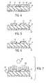
- FIG. 1is a cross-sectional view showing a lipophilic photoresist layer on top of a silicon wafer substrate
- FIG. 2is a cross-sectional view of a film of organotrialkoxysilane, photobase generator, and catalytic amount of water on top of the lipophilic photoresist layer
- FIG. 3is a cross-sectional view of the portion of the integrated circuit illustrated in FIG. 2, showing a first exposure step at wavelength ⁇ 1 ;
- FIG. 4is a cross-sectional view of the portion of the integrated circuit illustrated in FIG. 3, showing the polymerization of the exposed parts of organoarylalkoxysilane layer by the photogenerated base from the photobase generator and catalytic amount of water at first exposure step at wavelength ⁇ 1 ;
- FIG. 5is a cross-sectional view of the portion of the integrated circuit illustrated in FIG. 4, showing a self-aligned pattern formation step, following the washing away of the unpolymerized organoarylalkoxysilane with water/methanol solution;
- FIG. 6is a cross-sectional view of the portion of the integrated circuit illustrated in FIG. 5, showing a self-aligned pattern formation step, following the baking of the polymerized organoarylalkoxysilane layer;
- FIG. 7is a cross-sectional view of the portion of the integrated circuit illustrated in FIG. 6, showing a flood exposure step at wavelength ⁇ 2 ;
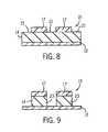
- FIG. 8s a cross-sectional view of the portion of the integrated circuit illustrated in FIG. 7 showing a post-exposure bake step
- FIG. 9is a cross-sectional view of the portion of the integrated circuit illustrated in FIG. 8 showing a develop step
- FIG. 10is plot of absorption spectra of representative organoarylalkoxysilane from 150 nm to 200 nm.
- the advantageous schemealso provides sub-lithographic feature resolution on the order smaller than the resolution limit of the first wavelength ⁇ 1 (the shorter of the dual wavelengths).
- a first exposure stepcomprising the advantageous process is performed on a portion of an integrated circuit (IC).
- the portionincludes a photoresist layer 14 provided on a substrate 12 .
- Substrate 12can be an IC wafer, a semiconductive material, an insulative material, a conductive material, layers above any of the listed materials, or a base layer.
- Substrate 12can be an industry standard silicon wafer. Substrate 12 is not described in a limiting fashion.
- Substrate 12can include insulative, conductive, or semiconductive layers above or below its top surface.
- the insulative, conductive or semiconductive layerscan be deposited or grown on substrate 12 or on layers above layers on substrate 12 .
- layer 14can be provided above base layers, intermediate layers, anti-reflective coatings, or other layers.
- Photoresist layer 14is selected to have photochemical reactions in response to electromagnetic radiation 16 from a first light source 18 (FIG. 3 ).
- Photoresist layer 14can be any conventional positive photoresist material.
- photoresist layer 14is comprised of a 193-nm or 248-nm wavelength photosensitive lipophilic polymeric material with the appropriate photoacid generator applied to substrate 12 at a thickness of 100-500 nm by spin coating.
- First light source 18can be any number of sources of electromagnetic radiation.
- First light source 18can be a single light source or multiple light sources for providing radiation 16 at a short wavelength.
- first light source 18provides radiation 16 at a short wavelength (193 nm, 248 nm) in the deep ultraviolet (DUV) or vacuum ultraviolet (157 nm, 126 nm), or extreme ultraviolet (EUV) range, such as, 11.4 nm, 13.4 nm.
- DUVdeep ultraviolet
- EUVextreme ultraviolet
- the short wavelength ⁇ 1 of radiation 16(also referred to as the short lithographic wavelength) preferably can polymerize organotrialkoxysilane monomers such as aryltriethoxysilane in the presence of photobase generators (PBG) such as o-nitrobenzoyl carbamates and urethanes, o-acyloxime, benzoin carbamate, oxime-urethanes, etc. and catalytic amount of water, as shown in Equation 1 below:
- PBGphotobase generators
- First light source 18can be a laser light source such as an F 2 excimer laser (157 nm), XeCl laser, ArF excimer laser (193 nm), KrF laser (248 nm), or laser-produced Xe plasma (13.4 nm, 11.4 nm) or discharge-produced plasma (at 13.4 nm, 11.4 nm) or other radiations such as electron beam, ion beam, gamma ray, etc.
- light source 18can be a laser light source that emits two or more wavelengths in various wavelength ranges, such as, an argon laser.
- Radiation 16 from first light source 18is provided via a mask or reticle 20 in accordance with a pattern on mask or reticle 20 to photoresist layer 14 .
- Mask or reticle 20is preferably a conventional photomask or reticle including a glass substrate (e.g., fused silica) and an opaque material (e.g., chromium).
- an optical systeme.g., one or more lens assemblies.
- a film 15(FIG. 2) of arylalkoxysilane monomer with a photobase generator, and catalytic amount of water is coated on top of the lipophilic photoresist layer 14 and exposed to the short wavelength light ⁇ 1 .
- a few monolayers of an adhesion promoter like hexamethyldisilazanemay be coated on top of the photoresist to improve the adhesion of the arylalkoxysilane monomer to the photoresist.
- arylalkoxysilane monomersare: pheny-t-butyl-ether triethoxysilane, 1-phenyl-1-phenyl-t-butylether diethoxysilane, and benzyl-t-butylether triethoxysilane. These monomers can be combined or mixed depending on desired characteristics.
- the monomerhas available bonds associated with the Si atoms that can be activated to promote polymerization by short wavelength exposure and subsequent developments.
- the monomerpreferably has a profile of light absorbance as a function of the wavelength in which absorbance is lower at the shorter wavelengths to achieve current resolution goals and absorbance is higher at the longer wavelength to which more conventional resists are sensitive. Although these characteristics are preferred, the characteristics are not necessarily required for a photoresist material to fall within the scope of any claim unless explicitly required by the claim.
- the photobase generatorUpon exposure through a photomask (mask 20 ), the photobase generator generates a photobase, which catalyzes the polymerization of the arylalkoxysilane monomer in the presence of water in the exposed part of film 15 (FIGS. 3 and 4 ). While the arylalkoxysilane monomer (see regions 19 ) is reasonably transparent at 157 nm, the poly(arylalkoxysilane) is quite opaque (see regions 17 ). The absorbance of the poly(arylalkoxysilane) (regions 17 ) is significantly higher at 193 nm than at 157 nm (see FIG. 10 ).
- Photoresist layer 14is preferably a positive photoresist that is transparent to radiation at longer ultraviolet (UV) wavelengths (e.g., 365 nm, 248 nm, or 193 nm) and is marginally or semi-transparent to radiation at shorter wavelengths (e.g., 157 nm, 126 nm, or 13.4 nm).
- UVultraviolet
- photoresist layer 14can be a photoresist conventionally used in 193 nm lithography, such as Sumitomo Chemical's PAR720TM, PAR707TM, or a photoresist used in 248 nm lithography such as Shipley's UV110TM—an environmentally stable chemically amplified photoresist (ESCAP).
- Film 15 and photoresist layer 14form a bi-layer photoresist with two distinct and separate layers.
- the top layer (film 15 )polymerizes and becomes opaque at longer wavelengths to which the bottom layer (layer 14 ) is sensitive.
- the bottom layercan be a more conventional photoresist material and unlike the top layer, the bottom layer cannot be patterned efficiently by the shorter wavelength radiation.
- polymerized areas or regions 17 of layer 14After the first exposure step of FIG. 3, pattern transfer from mask 20 has occurred, as represented by polymerized areas or regions 17 of layer 14 .
- Polymerized areas 17have feature resolution on the order of approximately one-half the wavelength to the wavelength of the short exposure wavelength of radiation 16 .
- polymerized region 17 created by exposure to a 157 nm radiationhas a feature resolution of approximately 72-157 nm.
- radiation 16 at a wavelength of 126 or 13.4 nmwould result in a possible resolution of approximately 63-126 nm or 6.7-13.4 nm, respectively.
- Polymerized areas or regions 17are preferably opaque or non-transparent to radiation at longer lithographic wavelengths (e.g., 365, 248, or 193 nm) conventionally used to expose photoresist layer 14 . Such opaqueness permits polymerized areas or regions 17 to serve as a self-aligned mask or reticle in a longer wavelength exposure step involving portion 10 (FIG. 7 ).
- lithographic wavelengthse.g., 365, 248, or 193 nm
- a second light source 28provides flood exposure of radiation 30 at a longer lithographic or exposure wavelength of, for example, 248 nm.
- the wavelength of radiation 30 and layer 14are selected such that exposed areas of layer 14 (i.e., areas not covered by polymerized areas or regions 17 ) are transparent to radiation 30 and undergo a photochemical reaction to become soluble (soluble areas or regions 21 in FIG. 8 ), while areas underneath polymerized areas or regions 17 will not be exposed to radiation 30 due to the opaqueness of polymerized areas or regions 17 and remain insoluble (insoluble areas or regions 23 in FIG. 8 ).
- First and second light sources 18 , 28can be the same light source that emits radiation at two wavelengths, i.e., the short and long UV lithographic wavelengths.
- light source 28can be an excimer laser, an ND:YAG laser, a frequency multiplied ND:YAG laser, a He-Ne scanning laser, or other light source.
- the pattern or image provided on mask 20will be fully transferred to photoresist layer 14 at a resolution determined by the first exposure step.
- the exposed areas of layer 14are soluble areas or regions 21 and the non-exposed areas of layer 14 or regions 23 (FIG. 9) (due to polymerized areas or regions 17 ) become insoluble areas (see FIGS. 8 and 9 ).
- soluble areas or regions 17 of layer 14are removed such that only cross-linked areas or regions 17 and insoluble areas or regions 21 of layer 14 remain on substrate 12 (FIG. 9 ).
- the developing steputilizes a solvent developer conventionally selected to develop material comprising layer 14 .
- photoresist used for 248 nm lithographycan use a 0.24N tetramethylammonium hydroxide developer to remove soluble areas or regions 21 .
- polymerized areas or regions 17become insoluble upon exposure to short lithographic wavelength radiation.
- polymerized areas or regions 17may undergo further chemical changes upon exposure to long lithographic wavelength radiation as long as it functions as a mask during the second exposure step.
- polymerized areas or regions 17remain after the developing step and aid in subsequent processing steps such as an etching step or a deposition step involving portion 10 .
- Regions 17can improve etch stability of the top layer relative to the photoresist layer during anisotropic etching because it can be converted to silicon dioxide (SiO 2 ) under plasma etching conditions.
- a photoresist conventionally used in longer wavelength lithographycan be patterned with radiation of a short lithographic wavelength. Even further, the pattern resolution is smaller than those achievable with longer wavelength lithography, pattern resolution on the order of the short lithographic wavelength. Even still further, possible mask overlay or alignment problems are obviated through a self-aligned mask generated during the patterning process.
- a line 102represents the absorbance (1/ ⁇ m) on a Y-axis 110 across X-axis 108 (wavelength ⁇ 1 ).
- a line 102similarly represents absorbance of poly(1-phenyl-1-phenyl-t-butylether siloxane)
- line 104represents poly(phenyl-t-butylether siloxane)
- a line 106similarly represents absorbance of poly(benzyl-t-butylether siloxane).
Landscapes
- Physics & Mathematics (AREA)
- General Physics & Mathematics (AREA)
- Engineering & Computer Science (AREA)
- Spectroscopy & Molecular Physics (AREA)
- Architecture (AREA)
- Structural Engineering (AREA)
- Condensed Matter Physics & Semiconductors (AREA)
- Manufacturing & Machinery (AREA)
- Computer Hardware Design (AREA)
- Microelectronics & Electronic Packaging (AREA)
- Power Engineering (AREA)
- Exposure And Positioning Against Photoresist Photosensitive Materials (AREA)
- Photosensitive Polymer And Photoresist Processing (AREA)
- Exposure Of Semiconductors, Excluding Electron Or Ion Beam Exposure (AREA)
Abstract
Description

Claims (22)
Priority Applications (9)
| Application Number | Priority Date | Filing Date | Title |
|---|---|---|---|
| US10/083,914US6764808B2 (en) | 2002-02-27 | 2002-02-27 | Self-aligned pattern formation using wavelenghts |
| CNB038025280ACN1299166C (en) | 2002-02-27 | 2003-02-21 | Self-aligned pattern formation using dual wavelengths |
| PCT/US2003/004960WO2003073165A2 (en) | 2002-02-27 | 2003-02-21 | Self-aligned pattern formation using dual wavelengths |
| KR10-2004-7012948AKR20040094706A (en) | 2002-02-27 | 2003-02-21 | Self-aligned pattern formation using dual wavelengths |
| AU2003211152AAU2003211152A1 (en) | 2002-02-27 | 2003-02-21 | Self-aligned pattern formation using dual wavelengths |
| JP2003571795AJP2005519456A (en) | 2002-02-27 | 2003-02-21 | Formation of self-aligned pattern using two wavelengths |
| DE60329371TDE60329371D1 (en) | 2002-02-27 | 2003-02-21 | SELF-ORIENTING STRUCTURAL EDUCATION USING TWO WAVELENGTHS |
| EP03743156AEP1478978B1 (en) | 2002-02-27 | 2003-02-21 | Self-aligned pattern formation using dual wavelengths |
| TW092104154ATWI278013B (en) | 2002-02-27 | 2003-02-27 | Self-aligned pattern formation using dual wavelengths |
Applications Claiming Priority (1)
| Application Number | Priority Date | Filing Date | Title |
|---|---|---|---|
| US10/083,914US6764808B2 (en) | 2002-02-27 | 2002-02-27 | Self-aligned pattern formation using wavelenghts |
Publications (2)
| Publication Number | Publication Date |
|---|---|
| US20030162135A1 US20030162135A1 (en) | 2003-08-28 |
| US6764808B2true US6764808B2 (en) | 2004-07-20 |
Family
ID=27753386
Family Applications (1)
| Application Number | Title | Priority Date | Filing Date |
|---|---|---|---|
| US10/083,914Expired - LifetimeUS6764808B2 (en) | 2002-02-27 | 2002-02-27 | Self-aligned pattern formation using wavelenghts |
Country Status (9)
| Country | Link |
|---|---|
| US (1) | US6764808B2 (en) |
| EP (1) | EP1478978B1 (en) |
| JP (1) | JP2005519456A (en) |
| KR (1) | KR20040094706A (en) |
| CN (1) | CN1299166C (en) |
| AU (1) | AU2003211152A1 (en) |
| DE (1) | DE60329371D1 (en) |
| TW (1) | TWI278013B (en) |
| WO (1) | WO2003073165A2 (en) |
Cited By (6)
| Publication number | Priority date | Publication date | Assignee | Title |
|---|---|---|---|---|
| US20040086800A1 (en)* | 2002-11-04 | 2004-05-06 | Meagley Robert P. | Photoactive adhesion promoter |
| US20040197676A1 (en)* | 2003-03-04 | 2004-10-07 | Jenspeter Rau | Method for forming an opening in a light-absorbing layer on a mask |
| US20060101513A1 (en)* | 2003-03-12 | 2006-05-11 | Infineon Technologies Ag | Method for operating a microprocessor |
| US20070241329A1 (en)* | 2006-04-17 | 2007-10-18 | Nec Electronics Corporation | Semiconductor integrated circuit and method for manufacturing same, and mask |
| US20080122106A1 (en)* | 2006-09-11 | 2008-05-29 | International Business Machines | Method to generate airgaps with a template first scheme and a self aligned blockout mask |
| US20090068594A1 (en)* | 2005-05-02 | 2009-03-12 | Tokyo Ohka Kogyo Co., Ltd. | Positive resist composition and method for forming resist pattern |
Families Citing this family (10)
| Publication number | Priority date | Publication date | Assignee | Title |
|---|---|---|---|---|
| DE10138105A1 (en)* | 2001-08-03 | 2003-02-27 | Infineon Technologies Ag | Photoresist and method for structuring such a photoresist |
| US7265366B2 (en)* | 2004-03-31 | 2007-09-04 | Asml Netherlands B.V. | Lithographic apparatus and device manufacturing method |
| WO2006085741A1 (en)* | 2005-02-09 | 2006-08-17 | Stichting Dutch Polymer Institute | Process for preparing a polymeric relief structure |
| US20070166649A1 (en)* | 2006-01-18 | 2007-07-19 | Cheng-Hung Yu | Method of forming a micro device |
| CN100465666C (en)* | 2006-01-24 | 2009-03-04 | 联华电子股份有限公司 | Method for manufacturing micro-component |
| JP4660826B2 (en)* | 2006-08-18 | 2011-03-30 | 山栄化学株式会社 | Method for forming resist pattern |
| KR101023077B1 (en)* | 2008-10-27 | 2011-03-24 | 주식회사 동부하이텍 | How to form a mask pattern |
| KR101888287B1 (en) | 2014-01-27 | 2018-08-13 | 도쿄엘렉트론가부시키가이샤 | System and method for shifting critical dimensions of patterned films |
| US9645495B2 (en) | 2014-08-13 | 2017-05-09 | Tokyo Electron Limited | Critical dimension control in photo-sensitized chemically-amplified resist |
| US11294273B2 (en)* | 2019-10-25 | 2022-04-05 | Innolux Corporation | Mask substrate and method for forming mask substrate |
Citations (6)
| Publication number | Priority date | Publication date | Assignee | Title |
|---|---|---|---|---|
| EP0098922A2 (en) | 1982-07-13 | 1984-01-25 | International Business Machines Corporation | Process for selectively generating positive and negative resist patterns from a single exposure pattern |
| US4704347A (en) | 1985-02-18 | 1987-11-03 | U.S. Philips Corporation | Method of manufacturing a semiconductor device, in which a photolacquer mask is formed by means of a two-layer lacquer system. |
| US4810601A (en)* | 1984-12-07 | 1989-03-07 | International Business Machines Corporation | Top imaged resists |
| EP0366503A2 (en) | 1988-10-28 | 1990-05-02 | Hewlett-Packard Company | Chemical compositions for improving photolithographic performance |
| US5876904A (en)* | 1996-01-16 | 1999-03-02 | Sumitomo Chemical Company, Ltd. | Method of providing a positive resist pattern |
| WO2003095026A1 (en) | 2002-05-13 | 2003-11-20 | Pflueger D Russell | Spinal disc therapy system |
Family Cites Families (4)
| Publication number | Priority date | Publication date | Assignee | Title |
|---|---|---|---|---|
| US5180655A (en)* | 1988-10-28 | 1993-01-19 | Hewlett-Packard Company | Chemical compositions for improving photolithographic performance |
| JP3192879B2 (en)* | 1994-07-28 | 2001-07-30 | トヨタ自動車株式会社 | Ceramic butterfly valve and method of manufacturing the same |
| JP3373147B2 (en)* | 1998-02-23 | 2003-02-04 | シャープ株式会社 | Photoresist film and pattern forming method thereof |
| FR2812450B1 (en)* | 2000-07-26 | 2003-01-10 | France Telecom | RESIN, TWO-LAYER RESIN FOR EXTREME ULTRAVIOLET (EUV) PHOTOLITHOGRAPHY AND METHOD FOR EXTREME ULTRAVIOLET (EUV) PHOTOLITHOGRAPHY |
- 2002
- 2002-02-27USUS10/083,914patent/US6764808B2/ennot_activeExpired - Lifetime
- 2003
- 2003-02-21EPEP03743156Apatent/EP1478978B1/ennot_activeExpired - Lifetime
- 2003-02-21CNCNB038025280Apatent/CN1299166C/ennot_activeExpired - Fee Related
- 2003-02-21DEDE60329371Tpatent/DE60329371D1/ennot_activeExpired - Lifetime
- 2003-02-21KRKR10-2004-7012948Apatent/KR20040094706A/ennot_activeCeased
- 2003-02-21AUAU2003211152Apatent/AU2003211152A1/ennot_activeAbandoned
- 2003-02-21WOPCT/US2003/004960patent/WO2003073165A2/enactiveApplication Filing
- 2003-02-21JPJP2003571795Apatent/JP2005519456A/enactivePending
- 2003-02-27TWTW092104154Apatent/TWI278013B/ennot_activeIP Right Cessation
Patent Citations (6)
| Publication number | Priority date | Publication date | Assignee | Title |
|---|---|---|---|---|
| EP0098922A2 (en) | 1982-07-13 | 1984-01-25 | International Business Machines Corporation | Process for selectively generating positive and negative resist patterns from a single exposure pattern |
| US4810601A (en)* | 1984-12-07 | 1989-03-07 | International Business Machines Corporation | Top imaged resists |
| US4704347A (en) | 1985-02-18 | 1987-11-03 | U.S. Philips Corporation | Method of manufacturing a semiconductor device, in which a photolacquer mask is formed by means of a two-layer lacquer system. |
| EP0366503A2 (en) | 1988-10-28 | 1990-05-02 | Hewlett-Packard Company | Chemical compositions for improving photolithographic performance |
| US5876904A (en)* | 1996-01-16 | 1999-03-02 | Sumitomo Chemical Company, Ltd. | Method of providing a positive resist pattern |
| WO2003095026A1 (en) | 2002-05-13 | 2003-11-20 | Pflueger D Russell | Spinal disc therapy system |
Non-Patent Citations (1)
| Title |
|---|
| International Search Report for International Application No. PCT/ US03/14960, Filing Date Feb. 12, 2003 (3 pages). |
Cited By (14)
| Publication number | Priority date | Publication date | Assignee | Title |
|---|---|---|---|---|
| US7611828B2 (en) | 2002-11-04 | 2009-11-03 | Meagley Robert P | Photoactive adhesion promoter |
| US20040086800A1 (en)* | 2002-11-04 | 2004-05-06 | Meagley Robert P. | Photoactive adhesion promoter |
| US7501230B2 (en)* | 2002-11-04 | 2009-03-10 | Meagley Robert P | Photoactive adhesion promoter |
| US20090076291A1 (en)* | 2002-11-04 | 2009-03-19 | Meagley Robert P | Photoactive adhesion promoter |
| US7229723B2 (en)* | 2003-03-04 | 2007-06-12 | Infineon Technologies Ag | Method for forming an opening in a light-absorbing layer on a mask |
| US20040197676A1 (en)* | 2003-03-04 | 2004-10-07 | Jenspeter Rau | Method for forming an opening in a light-absorbing layer on a mask |
| US20060101513A1 (en)* | 2003-03-12 | 2006-05-11 | Infineon Technologies Ag | Method for operating a microprocessor |
| US20090068594A1 (en)* | 2005-05-02 | 2009-03-12 | Tokyo Ohka Kogyo Co., Ltd. | Positive resist composition and method for forming resist pattern |
| US7816072B2 (en)* | 2005-05-02 | 2010-10-19 | Tokyo Ohka Kogyo Co., Ltd. | Positive resist composition and method for forming resist pattern |
| US20070241329A1 (en)* | 2006-04-17 | 2007-10-18 | Nec Electronics Corporation | Semiconductor integrated circuit and method for manufacturing same, and mask |
| US8278760B2 (en)* | 2006-04-17 | 2012-10-02 | Renesas Electronics Corporation | Semiconductor integrated circuit and method for manufacturing same, and mask |
| US20110163446A1 (en)* | 2006-09-11 | 2011-07-07 | International Business Machines Corporation | Method to generate airgaps with a template first scheme and a self aligned blockout mask and structure |
| US7863150B2 (en)* | 2006-09-11 | 2011-01-04 | International Business Machines Corporation | Method to generate airgaps with a template first scheme and a self aligned blockout mask |
| US20080122106A1 (en)* | 2006-09-11 | 2008-05-29 | International Business Machines | Method to generate airgaps with a template first scheme and a self aligned blockout mask |
Also Published As
| Publication number | Publication date |
|---|---|
| DE60329371D1 (en) | 2009-11-05 |
| TWI278013B (en) | 2007-04-01 |
| EP1478978B1 (en) | 2009-09-23 |
| JP2005519456A (en) | 2005-06-30 |
| US20030162135A1 (en) | 2003-08-28 |
| WO2003073165A3 (en) | 2003-10-16 |
| AU2003211152A1 (en) | 2003-09-09 |
| CN1620634A (en) | 2005-05-25 |
| KR20040094706A (en) | 2004-11-10 |
| TW200303573A (en) | 2003-09-01 |
| WO2003073165A2 (en) | 2003-09-04 |
| CN1299166C (en) | 2007-02-07 |
| EP1478978A2 (en) | 2004-11-24 |
Similar Documents
| Publication | Publication Date | Title |
|---|---|---|
| US6905621B2 (en) | Method for preventing the etch transfer of sidelobes in contact hole patterns | |
| US9235119B2 (en) | Exposure photolithography methods | |
| US9012132B2 (en) | Coating material and method for photolithography | |
| US8741551B2 (en) | Method and composition of a dual sensitive resist | |
| US7033735B2 (en) | Water soluble negative tone photoresist | |
| US6764808B2 (en) | Self-aligned pattern formation using wavelenghts | |
| CN108807150B (en) | Manufacturing method of semiconductor device | |
| US20060160028A1 (en) | Method of forming fine patterns of a semiconductor device | |
| CN101427348B (en) | Method for reducing minimum spacing in patterns | |
| US5455145A (en) | Method of manufacturing double layer resist pattern and double layer resist structure | |
| US8084185B2 (en) | Substrate planarization with imprint materials and processes | |
| US12050404B2 (en) | Photoresist with polar-acid-labile-group | |
| CN108983546A (en) | Lithographic method | |
| US20150316846A1 (en) | Method of Preparing and Using Photosensitive Material | |
| CN110941148A (en) | Manufacturing method of semiconductor device | |
| US7169716B2 (en) | Photosensitive lacquer for providing a coating on a semiconductor substrate or a mask | |
| CN108231550B (en) | Method for manufacturing semiconductor device | |
| US6514874B1 (en) | Method of using controlled resist footing on silicon nitride substrate for smaller spacing of integrated circuit device features | |
| Kudo et al. | Latest developments in photosensitive developable bottom anti-reflective coating (DBARC) | |
| US20040265748A1 (en) | Pattern transfer of an extreme ultraviolet imaging layer via flood exposure of contact mask layer (EUV CML) | |
| Richter et al. | CARL–advantages of thin-film imaging for leading-edge lithography | |
| KR20040079756A (en) | Method for Forming Micro Pattern of Semiconductor Device | |
| JPH10223503A (en) | Method of forming resist pattern | |
| KR20070109638A (en) | Pattern formation method of semiconductor device | |
| KR20050086992A (en) | Lithography method for increasing cd uniformity |
Legal Events
| Date | Code | Title | Description |
|---|---|---|---|
| AS | Assignment | Owner name:ADVANCED MICRO DEVICES, INC., CALIFORNIA Free format text:ASSIGNMENT OF ASSIGNORS INTEREST;ASSIGNORS:OKOROANYANWU, UZODINMA;BOTTELLI, ARMANDO C.;REEL/FRAME:012643/0859;SIGNING DATES FROM 20020221 TO 20020222 | |
| STCF | Information on status: patent grant | Free format text:PATENTED CASE | |
| FEPP | Fee payment procedure | Free format text:PAYOR NUMBER ASSIGNED (ORIGINAL EVENT CODE: ASPN); ENTITY STATUS OF PATENT OWNER: LARGE ENTITY | |
| FPAY | Fee payment | Year of fee payment:4 | |
| AS | Assignment | Owner name:GLOBALFOUNDRIES INC., CAYMAN ISLANDS Free format text:AFFIRMATION OF PATENT ASSIGNMENT;ASSIGNOR:ADVANCED MICRO DEVICES, INC.;REEL/FRAME:023119/0083 Effective date:20090630 | |
| FPAY | Fee payment | Year of fee payment:8 | |
| FPAY | Fee payment | Year of fee payment:12 | |
| AS | Assignment | Owner name:WILMINGTON TRUST, NATIONAL ASSOCIATION, DELAWARE Free format text:SECURITY AGREEMENT;ASSIGNOR:GLOBALFOUNDRIES INC.;REEL/FRAME:049490/0001 Effective date:20181127 | |
| AS | Assignment | Owner name:GLOBALFOUNDRIES U.S. INC., CALIFORNIA Free format text:ASSIGNMENT OF ASSIGNORS INTEREST;ASSIGNOR:GLOBALFOUNDRIES INC.;REEL/FRAME:054633/0001 Effective date:20201022 | |
| AS | Assignment | Owner name:GLOBALFOUNDRIES INC., CAYMAN ISLANDS Free format text:RELEASE BY SECURED PARTY;ASSIGNOR:WILMINGTON TRUST, NATIONAL ASSOCIATION;REEL/FRAME:054636/0001 Effective date:20201117 | |
| AS | Assignment | Owner name:GLOBALFOUNDRIES U.S. INC., NEW YORK Free format text:RELEASE BY SECURED PARTY;ASSIGNOR:WILMINGTON TRUST, NATIONAL ASSOCIATION;REEL/FRAME:056987/0001 Effective date:20201117 |