US6763057B1 - Vector modulation system and method for wideband impulse radio communications - Google Patents
Vector modulation system and method for wideband impulse radio communicationsDownload PDFInfo
- Publication number
- US6763057B1 US6763057B1US09/538,519US53851900AUS6763057B1US 6763057 B1US6763057 B1US 6763057B1US 53851900 AUS53851900 AUS 53851900AUS 6763057 B1US6763057 B1US 6763057B1
- Authority
- US
- United States
- Prior art keywords
- time
- signal
- pulses
- pulse
- time delay
- Prior art date
- Legal status (The legal status is an assumption and is not a legal conclusion. Google has not performed a legal analysis and makes no representation as to the accuracy of the status listed.)
- Expired - Fee Related
Links
- 238000000034methodMethods0.000titleclaimsabstractdescription59
- 238000004891communicationMethods0.000titleclaimsdescription26
- 230000003111delayed effectEffects0.000claimsabstractdescription45
- 230000004044responseEffects0.000claimsdescription32
- 230000000737periodic effectEffects0.000claimsdescription27
- 238000000926separation methodMethods0.000claimsdescription15
- 230000001360synchronised effectEffects0.000claimsdescription4
- 238000012935AveragingMethods0.000abstractdescription3
- 238000001514detection methodMethods0.000abstractdescription2
- 108091006146ChannelsProteins0.000description68
- 230000006870functionEffects0.000description26
- 238000005314correlation functionMethods0.000description15
- 238000010586diagramMethods0.000description11
- 238000001228spectrumMethods0.000description11
- 230000005540biological transmissionEffects0.000description10
- 230000008901benefitEffects0.000description6
- 230000008569processEffects0.000description6
- 238000005070samplingMethods0.000description6
- 238000004364calculation methodMethods0.000description5
- 238000009499grossingMethods0.000description5
- 238000012905input functionMethods0.000description5
- 230000002087whitening effectEffects0.000description5
- 230000003044adaptive effectEffects0.000description4
- 238000012937correctionMethods0.000description4
- 230000007613environmental effectEffects0.000description4
- 230000010354integrationEffects0.000description4
- 238000012545processingMethods0.000description4
- 238000006243chemical reactionMethods0.000description3
- 238000005516engineering processMethods0.000description3
- 230000006872improvementEffects0.000description3
- 238000013507mappingMethods0.000description3
- 239000000463materialSubstances0.000description3
- 238000005259measurementMethods0.000description3
- 230000001960triggered effectEffects0.000description3
- 230000002411adverseEffects0.000description2
- 230000000295complement effectEffects0.000description2
- 230000001934delayEffects0.000description2
- 230000001419dependent effectEffects0.000description2
- 230000000694effectsEffects0.000description2
- 238000001914filtrationMethods0.000description2
- 230000036540impulse transmissionEffects0.000description2
- 230000007774longtermEffects0.000description2
- 230000035515penetrationEffects0.000description2
- 230000000644propagated effectEffects0.000description2
- 230000009467reductionEffects0.000description2
- 230000007480spreadingEffects0.000description2
- 238000012546transferMethods0.000description2
- 238000009825accumulationMethods0.000description1
- 238000013459approachMethods0.000description1
- 229910002056binary alloyInorganic materials0.000description1
- 230000008859changeEffects0.000description1
- 230000008878couplingEffects0.000description1
- 238000010168coupling processMethods0.000description1
- 238000005859coupling reactionMethods0.000description1
- 125000004122cyclic groupChemical group0.000description1
- 230000000593degrading effectEffects0.000description1
- 238000013461designMethods0.000description1
- 238000011161developmentMethods0.000description1
- 230000003292diminished effectEffects0.000description1
- 230000036039immunityEffects0.000description1
- 230000001771impaired effectEffects0.000description1
- 238000007689inspectionMethods0.000description1
- 230000007246mechanismEffects0.000description1
- 230000000149penetrating effectEffects0.000description1
- 230000001902propagating effectEffects0.000description1
- 238000005316response functionMethods0.000description1
- 230000035945sensitivityEffects0.000description1
- 230000003595spectral effectEffects0.000description1
- 230000006641stabilisationEffects0.000description1
- 238000011105stabilizationMethods0.000description1
- 238000012360testing methodMethods0.000description1
Images


Classifications
- H—ELECTRICITY
- H04—ELECTRIC COMMUNICATION TECHNIQUE
- H04B—TRANSMISSION
- H04B1/00—Details of transmission systems, not covered by a single one of groups H04B3/00 - H04B13/00; Details of transmission systems not characterised by the medium used for transmission
- H04B1/69—Spread spectrum techniques
- H04B1/7163—Spread spectrum techniques using impulse radio
- H04B1/7176—Data mapping, e.g. modulation
- H—ELECTRICITY
- H04—ELECTRIC COMMUNICATION TECHNIQUE
- H04L—TRANSMISSION OF DIGITAL INFORMATION, e.g. TELEGRAPHIC COMMUNICATION
- H04L25/00—Baseband systems
- H04L25/38—Synchronous or start-stop systems, e.g. for Baudot code
- H04L25/40—Transmitting circuits; Receiving circuits
- H04L25/49—Transmitting circuits; Receiving circuits using code conversion at the transmitter; using predistortion; using insertion of idle bits for obtaining a desired frequency spectrum; using three or more amplitude levels ; Baseband coding techniques specific to data transmission systems
- H04L25/4902—Pulse width modulation; Pulse position modulation
- H—ELECTRICITY
- H04—ELECTRIC COMMUNICATION TECHNIQUE
- H04B—TRANSMISSION
- H04B1/00—Details of transmission systems, not covered by a single one of groups H04B3/00 - H04B13/00; Details of transmission systems not characterised by the medium used for transmission
- H04B1/69—Spread spectrum techniques
- H04B1/707—Spread spectrum techniques using direct sequence modulation
- H04B1/709—Correlator structure
- H04B1/7095—Sliding correlator type
- H—ELECTRICITY
- H04—ELECTRIC COMMUNICATION TECHNIQUE
- H04B—TRANSMISSION
- H04B1/00—Details of transmission systems, not covered by a single one of groups H04B3/00 - H04B13/00; Details of transmission systems not characterised by the medium used for transmission
- H04B1/69—Spread spectrum techniques
- H04B1/7163—Spread spectrum techniques using impulse radio
- H04B1/7183—Synchronisation
Definitions
- the present inventionrelates generally to wideband impulse radio systems. More particularly, this invention pertains to systems and methods for modulating and demodulating wideband impulse radio signals.
- Impulse Radioincluding Impulse Radar
- IRImpulse Radar
- U.S. Pat. No. 4,641,317issued Feb. 3, 1987
- U.S. Pat. No. 4,813,057issued Mar. 14, 1989
- U.S. Pat. No. 4,979,186issued Dec. 18, 1990
- U.S. Pat. No. 5,303,108issued Nov. 8, 1994
- the disclosure of each of these patentsis incorporated in this patent specification by reference.
- Impulse radio systemsare generally characterized by their transmission of short duration, broad band pulses on a relatively low duty cycle.
- these pulsesmay approach a Gaussian monocycle, where the instantaneous pulse bandwidth is on the order of the center frequency.
- the short pulse, low duty cycle mechanismproduces a processing gain that may be utilized for interference rejection and channelization. Because of the extremely wide instantaneous bandwidth of the pulse, the available processing gain far exceeds what is achieved using typical conventional spread spectrum methods. This enables the utilization of many more channels at higher dynamic ranges and higher data rates than are available in the typical conventional spread spectrum system.
- Impulse radio systemshave further advantages in the resistance to multipath effect. Because impulse radio signals are divided in time rather than in frequency, time related effects, such as multipath interference, can be separated, resulting in lower average power and higher reliability for a given power level.
- Impulse radio techniquesare also useful in radar systems.
- Impulse radar systemsenjoy the combined advantages of very short pulses at relatively low frequencies.
- the short pulsesresult in high resolution and the low frequency gives relatively high material penetration. If a radar system used a pulse of equivalent bandwidth at a higher carrier frequency, the material penetration properties would usually be impaired.
- This combined advantageenables IR radio to be used for ground penetrating radar for inspection of bridges, roads, runways, utilities and the like, and security applications, and to “see” through walls for emergency management situations.
- Impulse radio systemsare not limited to transmitting and receiving Gaussian monocycle pulses.
- some basic impulse radio transmittersattempt to emit short Gaussian monocycle pulses having a tightly controlled average pulse-to-pulse interval.
- a Gaussian monocycleis the first derivative of the Gaussian function.
- a perfect Gaussian pulseis not achievable. In the frequency domain, this results in a slight reduction in the signal bandwidth.
- the signals transmitted by an IR transmitterincluding Gaussian monocycles, signals having multiple cycles in a Gaussian envelope, and their real world variations, are sometimes called impulses.
- the Gaussian monocycle waveformis naturally a wide bandwidth signal, with the center frequency and the bandwidth dependent on the width of the pulse. The bandwidth is approximately 160% of the center frequency.
- the center frequency of a monocycle pulseis approximately the reciprocal of its length, and its bandwidth is approximately equal to 1.6 times the center frequency.
- impulse radio systemscan be implemented where the transmitted and/or received signals have waveforms other than an ideal Gaussian monocycle.
- Pulse position modulationis a form of time modulation in which the value of each instantaneous value or sample of a modulating signal (e.g., a voice or data signal) is caused to change or modulate the position in time of a pulse. In the frequency domain, pulse position modulation distributes the energy over more frequencies.
- the time position(pulse-to-pulse interval) is preferably varied on a pulse-by-pulse basis by two separate components: an information component and a pseudo-random code component.
- an information componente.g., a spread spectrum radio system
- a pseudo-random code componente.g., a pseudo-random code component.
- Prior art spread spectrum radio systemsmake use of pseudo-random codes to spread a narrow band information signal over a relatively wide band of frequencies. A spread spectrum receiver then correlates these signals to retrieve the original information signal.
- impulse radio systemsachieve spreading through the spectrum of the waveform and thus do not need the pseudo-random code for energy spreading.
- the pseudo-random codeis used to smooth the comb spectrum, reject interference, and for channelization.
- impulse radio transmitterscan use pulse widths of between 20 and 0.1 nanoseconds (ns) and pulse-to-pulse intervals of between 2 and 5000 ns. These narrow monocycle pulses have an inherently wide bandwidth. This bandwidth is the range of frequencies in which one or more signal characteristics fall within specified limits, such as for example, six dB below the peak spectral density.
- the pseudo-random noise (PN) code componentis used for different purposes: channelization; energy smoothing in the frequency domain; and interference resistance.
- Channelizationis a procedure employed to divide a communications path into a number of channels.
- PN codescreate channels, if there is low correlation and/or interference among the codes being used. If there were a large number of uncoded impulse radio users within a confined area, there might be mutual interference. Further, while the use of the PN coding minimizes that interference, as the number of users rises the probability of an individual pulse from one user's sequence being received simultaneously with a pulse from another user's sequence increases.
- impulse radio systemscan be designed so that they do not depend on receiving every pulse.
- the impulse radio receivercan perform a correlating, synchronous receiving function (at the RF level) that uses a statistical sampling of many pulses to recover the transmitted information.
- Advanced impulse radio systemsmay utilize multiple pulses to transmit each data bit of information, and each pulse may be dithered in time to further smooth the spectrum to reduce interference and improve channelization. These systems may also include a sub-carrier for improved interference resistance and implementation advantages.
- each “bit” of transmitted informationcan be represented by a single pulse, with no coding component.
- Energy smoothing in the frequency domaininsures that impulse radio transmissions interfere minimally with conventional radio systems.
- optimal energy smoothingis obtained by applying to each pulse a PN code component time dither having a much larger magnitude than the information component time dither.
- the PN codingcan also make impulse radio highly resistant to interference from all radio communications systems, including from other impulse radio transmitters. This is critical, as any other signals within the band occupied by an impulse signal can act as interference to the impulse radio. Because there are no unallocated bands at or above 1 GHz available for impulse radio systems, they must share spectrum with other conventional and impulse radios without being adversely affected. Using a PN code can help impulse systems discriminate between the intended impulse transmission and transmissions from others.
- the impulse radio transmittergenerally includes a time base, such as a voltage-controlled oscillator, that generates a periodic timing signal with sub-nanosecond timing accuracy.
- the periodic timing signalis supplied to a code source and a code time modulator.
- the code sourceis typically a storage device for storing pseudo-random noise (PN) codes that have low cross correlation among the codes in a set and will include means for generating a code signal representative of the code sequence.
- PNpseudo-random noise
- the code sourcemonitors the periodic timing signal to permit the code signal to be synchronized to the code time modulator.
- the code time modulatoruses the code signal to modulate the periodic timing signal for channelization and smoothing of a final emitted impulse radio signal. The output of the code time modulator is called the coded timing signal.
- the impulse radio receiveris a direct conversion receiver with a single conversion stage that coherently converts a series of pulses into a baseband signal.
- the baseband signalis the information channel for the basic impulse radio communications system.
- pulse trainsnot single pulses, are used for communications.
- the impulse radio transmitter in such systemsgenerates a train of pulses for each bit of information.
- the data rate of such an impulse radio transmissionis only a fraction of the periodic timing signal used as a time base.
- Each data bitmodulates the time position of many of the pulses of the periodic timing signal. This yields a modulated, coded timing signal that comprises a train of identical pulses for each single data bit.
- Some impulse radio receiverstypically integrate 200 or more pulses to yield the baseband output.
- Other systemsuse a “one pulse per bit” information transmission scheme. The number of pulses over which the receiver integrates is dependent on a number of variables, including pulse rate, bit rate, interference levels, and range.
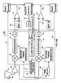
- the transmitter 602(FIG. 1 b ) comprises a time base 604 that generates a periodic timing signal 606 .
- the time base 604typically comprises a voltage controlled oscillator (VCO), or the like, having a high timing accuracy and low jitter, on the order of picoseconds (ps).
- VCOvoltage controlled oscillator
- the voltage control to adjust the VCO center frequencyis set at calibration to the desired center frequency used to define the transmitter's nominal pulse repetition rate.
- the periodic timing signal 606is supplied to a precision timing generator 608 .
- the precision timing generator 608supplies synchronizing signals 610 to the code source 612 and utilizes the code source output signal 614 together with an internally generated subcarrier signal (which is optional) and an information signal 616 to generate a modulated, coded timing signal 618 .
- the code source 612comprises a storage device such as a random access memory (RAM), read only memory (ROM), or the like, for storing suitable PN codes and for outputting the PN codes as a code signal 614 .
- RAMrandom access memory
- ROMread only memory
- maximum length shift registers or other computational meanscan be used to generate the PN codes.
- An information source 620supplies the information signal 616 to the precision timing generator 608 .
- the information signal 616can be any type of intelligence, including digital bits representing voice, data, imagery, or the like, analog signals, or complex signals.
- a pulse generator 622uses the modulated, coded timing signal 618 as a trigger to generate output pulses.
- the output pulsesare sent to a transmit antenna 624 via a transmission line 626 coupled thereto.
- the output pulsesare converted into propagating electromagnetic pulses by the transmit antenna 624 .
- the electromagnetic pulsesare called the emitted signal, and propagate to an impulse radio receiver 702 , such as shown in FIG. 1 a , through a propagation medium, such as air, in a radio frequency embodiment.
- the emitted signalis wide-band or ultrawide-band, approaching a monocycle pulse.
- the emitted signalcan be spectrally modified by filtering of the pulses. This filtering will usually cause each monocycle pulse to have more zero crossings (more cycles) in the time domain.
- the impulse radio receivercan use a similar waveform as the template signal in the cross correlator for efficient conversion.
- the receiver 702(FIG. 1 a ) is designed for reception of digital data wherein one or more pulses are transmitted for each data bit and comprises a receive antenna 704 for receiving a propagated impulse far radio signal 706 .
- a received signal 708 from the receive antenna 704is coupled to a cross correlator or sampler 710 to produce, a baseband output 712 .
- the cross correlator or sampler 710includes multiply and integrate functions together with any necessary filters to optimize signal to noise ratio.
- the receiver 702also includes a precision timing generator 714 , which receives a periodic timing signal 716 from a receiver time base 718 .
- This time base 718is adjustable and controllable in time, frequency, or phase, as required by a lock loop in order to lock on the received signal 708 .
- the precision timing generator 714provides synchronizing signals 720 to the code source 722 and receives a code control signal 724 from the code source 722 .
- the precision timing generator 714utilizes the periodic timing signal 716 and code control signal 724 to produce a coded timing signal 726 .
- the template generator 728is triggered by this coded timing signal 726 and produces a train of template signal pulses 730 ideally having waveforms substantially equivalent to each pulse of the received signal 708 .
- the code for receiving a given signalis the same code utilized by the originating transmitter 602 to generate the propagated signal 706 .
- the timing of the template pulse train 730matches the timing of the received signal pulse train 708 , allowing the received signal 708 to be synchronously sampled in the correlator 710 .
- the correlator 710ideally comprises a multiplier followed by a short term integrator to sum the multiplier product over the pulse interval. Further examples and details of correlation and sampling processes can be found in commonly owned U.S. Pat. Nos. 4,642,317, 4,813,057, and 4,979,186, which are incorporated herein by reference, and commonly owned and co-pending application Ser. No. 09/356,384, filed Jul. 16, 1999, titled: “Baseband Signal Converter Device for a Wideband Impulse Radio Receiver,” which is also incorporated herein by reference.
- the output of the correlator 710(FIG. 1 a ), also called a baseband signal 712 , is coupled to a subcarrier demodulator 732 , which demodulates the subcarrier information signal from the subcarrier.
- the output of the subcarrier demodulator 732is then filtered or integrated in a pulse summation stage 734 .
- the pulse summation stageproduces an output representative of the sum of a number of pulse signals comprising a single data bit.
- the output of the pulse summation stage 734is then compared with a nominal zero (or reference) signal output in a detector stage 738 to determine an output signal 739 representing an estimate of the original information signal 616 .
- the baseband signal 712is also input to a low pass filter 742 (also referred to as lock loop filter 742 ).
- a control loopcomprising the low pass filter 742 , time base 718 , precision timing generator 714 , template generator 728 , and correlator 710 is used to generate a filtered error signal 744 .
- the filtered error signal 744provides adjustments to the adjustable time base 718 to time position the periodic timing signal 726 in relation to the position of the received signal 708 .
- transceiver embodimentsubstantial economy can be achieved by sharing part or all of several of the functions of the transmitter 602 and receiver 702 . Some of these include the time base 718 , precision timing generator 714 , code source 722 , antenna 704 , and the like.
- the circuit or device in an impulse radio receiver that converts the received impulses into a baseband signalis sometimes referred to as a cross-correlator or sampler.
- the baseband signal converter of an impulse radio receivertypically integrates one or more pulses to recover the baseband signal that contains the transmitted information.
- a cross-correlator device usable in an impulse radio receiveris described in U.S. Pat. No. 5,677,927, issued Oct. 14, 1997, and assigned to Time Domain Corporation. The disclosure of the '927 Patent is incorporated in this specification by reference.
- prior art wideband impulse radio systemstypically use a binary (or scalar) modulation/demodulation scheme in which the transmitter emits a wideband pulse whose time position is varied in response to two separate components: an information component and a pseudo-random (PN) code component.
- the PN code componentfunctions, in a general sense, as a CDMA (Code Division Multiple Access) channel sequence.
- Binary time shift modulationcan be implemented by shifting the coded time position by an additional amount (that is, in addition to the PN code dither) in response to the information signal.
- the information componentprovides a modulation on the order of 1 ⁇ 4 cycle of the pulse waveform.
- correlationoccurs to determine if the transmitted pulse is early or late, with the result of this determination defining whether a digital “1” or “0” has been transmitted.
- Multiple pulsescan be combined to improve the signal-to-noise ratio of the received signal, but this will cause a reduction in the rate at which data can be transmitted and received.
- a typical prior art m-ary modulation scheme used in narrow band radio systemsmight use two correlators receiving the same signal shifted 90 degrees in phase. This yields a correlation function as shown in FIG. 2 where the I and Q channels represent the outputs of the two correlators such that the Q channel is shifted 90 degrees from the I channel.
- Four potential modulation states M 1 -M 4are shown as an example of the case where M is four. When these two functions are plotted with respect to one another, the plot of FIG. 3 results. The four modulation states M 1 -M 4 are also shown in FIG. 3 .
- FIG. 4is a plot of the two correlation functions when the sampling sine wave is 180 degrees.
- FIG. 5shows these two functions plotted versus one another. It can be seen that when the modulation is separated by 180 degrees, the I correlator generates an inverted version of the output of the Q correlator. Thus, only two end points may be observed and, accordingly, fewer modulation states can be achieved using those end points and without resorting to amplitude variations.
- a method and systemhave been developed for time modulating and demodulating wideband impulse radio signals to provide a data transmission rate in excess of one bit per pulse, while maintaining an acceptable bit error rate in the presence of noise.
- This improved data rateis achieved by a novel modulation scheme within the information component of the wideband impulse radio signal.
- the modulator portion of the impulse radio transmitterimposes multiple modulation states on each transmitted pulse.
- Multiple correlators (or baseband signal converters) in the impulse radio receivercan distinguish each of the multiple states so that each pulse can now communicate two or more bits of data.
- each transmitted pulseis modulated into one of four different time positions spanning a cycle of the pulse interval.
- four demodulation vector states, or quadrantsare determined relative to the correlator response function. These four transmitted time positions and demodulation vector quadrants correspond to two data bits of information: (0,0), (0,1), (1,0), and (1,1).
- each pulseconstitutes a “symbol”, with data transmitted at n bits per symbol and one pulse per symbol.
- a sequence of multiple pulses, each modulated into the same relative time position or modulation position by the information signalcan be combined to form a single n bit data symbol by summing pulses to form a symbol.
- a variation of this embodimentrequires the transmission and summation of a sequence of multiple pulses, each modulated into different time positions or modulation positions, to form a single n bit data symbol.
- two correlatorsare used to demodulate the information component from each pulse, i.e., to estimate the values of the data bits being transmitted with each pulse.
- the first correlatorobserves each pulse at a reference point (the “I” channel) according to a reference clock while a second correlator observes each pulse at a time offset point (the “J” channel) from the reference clock.
- the second correlatoris responsive to a decode timing signal used to trigger operation of the first correlator, but delayed by an amount of time, typically one-quarter to one-half of the RF pulse period.
- Each correlatortypically includes an integrator and may include a sample and hold or track and hold circuit to overcome droop and other imperfections in practical high speed integrator circuits. These circuits are collectively referred to as the “correlator” for the remainder of this document.
- the outputs from the correlatorsare supplied to a lock loop circuit that is responsible for acquiring and locking, i.e. synchronizing, the receiver time base with the transmitter time base.
- the lock loop circuitmay include a thresholding circuit for acquiring the signal generated by the transmitter.
- the output of the I correlatoris compared in a first comparator to a first reference voltage and the output of the J correlator is compared in a second comparator to a second reference voltage in order to estimate the values of the data bits being transmitted with each pulse.
- the reference voltagesmay be equal and may be adjusted with respect to each other in order to improve identification of the data bits transmitted with each pulse.
- the outputs of both correlatorsare compared in a comparator to a long term average output from each correlator, with the outputs of the comparators to achieve an estimate of the value of the two data bits associated with each pulse.
- the output of the I correlatoris summed with the output of the J correlator and the output of the I correlator is subtracted from the output of the J correlator.
- the summed value (I+J)is then compared in a first comparator to a first reference voltage and the subtracted value (I ⁇ J) is compared in a second comparator to a second reference voltage in order to estimate the values of the data bits being transmitted with each pulse.
- the reference voltagesmay be equal and may be adjusted with respect to each other to improve identification of the data bits transmitted with each pulse.
- the analog I and J channel outputs from the first and second correlatorsare digitized and sent to a processor.
- the processorcontains vector demodulation algorithms to estimate the value of the n data bits associated with each pulse.
- the processorcompares the digitized values of the I and J channel outputs for each pulse to a table of stored I and J channel value pairs. Four specified ranges of I and J channel value pairs are grouped in memory, with each group corresponding to expected scatter points associated with one of the four modulation states. Based on the results of this comparison, the processor provides an output representing the two data bits associated with that pulse: (0,0), (0,1), (1,0), or (1,1).
- the correlators and processorare then reset, so that processing of the next pulse can proceed.
- the processorcan implement additional algorithms to make adjustments in real time to maintain an acceptable degree of separation between the modulation states.
- the processorcan separately monitor the average values of the I and J channel outputs to determine if an acceptable amount of separation exists between modulation states.
- the processorcan store a sequence of scatter points generated by the I and J channel outputs and periodically compare them to an idealized plot of the expected scatter points in each modulation state or quadrant, as stored in memory. In either case, the processor can compensate for error by providing a signal to the J channel timing delay circuit that will vary the amount of delay between triggering of the I and J channel correlators, until separation among the four modulation states is optimized.
- the two transceiverscan exchange signal performance information to determine the optimal modulation states for a given propagation path. This improvement is potentially significant since the pulse shape can be modified by objects or reflectors in the propagation path.
- FIG. 1 a and FIG. 1 bare block diagrams of a transmitter and receiver used in a wideband impulse radio communications system.
- FIG. 2shows the outputs of reference (I channel) and delayed (Q channel) correlators for a range of received pulse times using idealized sinusoidal wave shapes in a prior art m-ary modulation scheme.
- FIG. 3is a polar plot of four possible modulation states of the I and Q channels generated in accordance with the correlator outputs shown in FIG. 2 .
- FIG. 4is a plot of the two correlation functions in a conventional m-ary modulation system when the sampling sine wave is delayed 180 degrees.
- FIG. 5is a polar plot of the possible modulation states of the I and Q channels generated in accordance with the correlator outputs shown in FIG. 4 .
- FIG. 6is a plot of the correlation functions for a UWB system that transmits a Gaussian doublet and wherein the receiver uses a simple sampler for correlation.
- FIG. 7is a polar plot of four possible modulation states of the I and J channels generated in accordance with the correlator outputs shown in FIG. 6 .
- FIG. 8is a plot of a linear combination (I+J and I ⁇ J) of the I and J correlator outputs shown in FIG. 6 .
- FIG. 9is a polar plot of six possible modulation states of the I and J channels generated in accordance with the combined correlator outputs shown in FIG. 8 .
- FIG. 10is a plot of the I and J correlator outputs where the input function is the second derivative of the Gaussian pulse and the correlation function is a simple sampling function, or the case where the input and correlation functions are the first derivative of the Gaussian pulse.
- FIG. 11is a polar plot of four possible modulation states of the I and J channels generated in accordance with the correlator outputs shown in FIG. 10 .
- FIG. 12is a plot of a linear combination (I+J and I ⁇ J) of the I and J correlator outputs shown in FIG. 10 .
- FIG. 13is a polar plot of some of the possible modulation states of the I and J channels generated in accordance with the combined correlator outputs shown in FIG. 12 .
- FIG. 14is a plot of I and J correlator outputs where the correlation function is the third derivative of the Gaussian function and where the J correlator ouput is delayed such that the second peak of the I correlator output coincides with the first peak of the J correlator output.
- FIG. 15is a polar plot of four possible modulation states of the I and J channels generated in accordance-with the correlator outputs shown in FIG. 14 .
- FIG. 16is a plot of a linear combination (I+J and I ⁇ J) of the I and J correlator outputs shown in FIG. 14 .
- FIG. 17is a polar plot of some of the possible modulation states of the I and J channels generated in accordance with the combined correlator outputs shown in FIG. 16 .
- FIG. 18is a plot of the I and J correlator outputs as shown in FIG. 10, but with a different delay between the correlators.
- FIG. 19is a polar plot of the possible modulation states of the I and J channels generated in accordance with the correlator outputs shown in FIG. 18 .
- FIG. 20is a plot of a linear combination (I+J and I ⁇ J) of the I and J correlator outputs shown in FIG. 18 .
- FIG. 21is a polar plot of some of the possible modulation states of the I and J channels generated in accordance with the combined correlator outputs shown in FIG. 20 .
- FIG. 22is a block diagram of one embodiment of a wideband impulse radio transmitter used in the communications system of the present invention.
- FIG. 23 ais a block diagram of a first embodiment of a wideband impulse radio receiver used in the communications system of the present invention.
- FIG. 23 bis a block diagram of a second embodiment of a wideband impulse radio receiver having track and hold circuits used in the communications system of the present invention.
- FIG. 23 cis a block diagram of a signal combiner circuit that may be used in conjunction with the system and method of this invention.
- FIG. 23 dis a block diagram of an alternative embodiment of the signal combiner that may be used in conjunction with the system and method of this invention.
- FIG. 24is a plot of correlator output versus time in response to an actual received UWB pulse that may be distorted by building walls or other environmental conditions after transmission, wherein the transmitted pulse is similar to that shown in FIG. 14 .
- FIG. 25is a polar plot of the I and J channel outputs generated by wideband RF pulses having a non-idealized wave shape.
- FIG. 26is a polar plot of the four possible modulation states of the I and J channels generated in accordance with an embodiment of the vector modulation method of this invention, showing an angular skew and DC offset created by reception of a non-idealized pulse wave form and the I and J channel outputs shown in FIG. 25 .
- FIGS. 27 a and 27 bare block diagrams of a third embodiment of a wideband impulse radio receiver used in the communications system of the present invention.
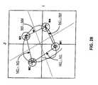
- FIG. 28is a plot of the I and J channel scatter from the wideband impulse radio receiver of FIGS. 27 a and 27 b.
- FIG. 29is a block diagram showing the data path of another embodiment of the system of the present invention using quad flipped time modulation (QFTM).
- QFTMquad flipped time modulation
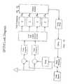
- FIG. 30is a block lock loop diagram of the QFTM system of FIG. 29 .
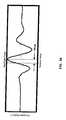
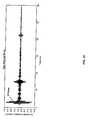
- FIG. 31is a plot of a correlator output versus time for a real world received UWB pulse.
- FIG. 32is a plot of the correlation functions from two delayed correlators wherein the pulse waveform corresponds to the “1 st pulse” portion of FIG. 31 .
- FIG. 33is a polar plot of the four possible modulation states of the I and J channels generated in accordance with the correlator outputs shown in FIG. 32 .
- FIG. 34is a plot of a linear combination (I+J and I ⁇ J) of the I and J correlator outputs shown in FIG. 32 .
- FIG. 35is a polar plot of some of the possible modulation states of the I and J channels generated in accordance with the combined correlator outputs shown in FIG. 34 .
- FIG. 36is a plot of the correlator outputs, I and J, from FIG. 6 and an inverter version of the correlator outputs, I and J.
- FIG. 37is a polar plot of four possible modulation states of the I and J channels generated in accordance with the correlator outputs shown in FIG. 36 .
- FIG. 38is a plot of a linear combination (I+J and I ⁇ J) of the I and J correlator outputs shown in FIG. 36 and an inverted version of the linear combination (I+J and I ⁇ J).
- FIG. 39is a polar plot of four possible modulation states of the I and J channels generated in accordance with the correlator outputs shown in FIG. 38 .
- the received pulseis so short that the correlation function is not identical for successive cycles. In fact, it can be so short that it essentially decays in the adjacent cycle. This gives rise to correlation functions that are non-sinusoidal and modulation state plots that are slightly to severely non-circular. This creates unique problems in modulation state design for these systems, as compared to prior art m-ary modulation techniques as reflected in FIGS. 2 and 3.
- FIG. 6represents the correlation function for a UWB system that transmits a Gaussian doublet and the receiver has a simple sampler. Although a Gaussian doublet is used in this example, various other input waveforms may be used as well.
- the I channelrepresents the output of the early channel as a function of pulse delay
- the J channelrepresents the corresponding output of the delayed channel.
- the points labeled “M 1 ”, “M 2 ”, “M 3 ”, and “M 4 ”correspond to the magnitudes of the I and J correlator outputs at points delayed in time.
- the relative magnitudes of the I and J outputs from FIG. 6are plotted on FIG.
- the vector position of the point (I, J)is a function of the time delay of the J correlator with respect to the I correlator.
- the plot of FIG. 7is produced. The locus is seen to begin at the origin and travel through two extremes in each axis and then return to the origin. Note that there is not a strict quadrature relationship between these two functions, that is, where one passes through a maximum, the other does not pass through zero. Note that modulation state M 1 is placed at the first maximum of correlator I output.
- the output of the J correlatoris not zero but ⁇ 0.4.
- M 1 -M 4Four potential modulation states are identified by M 1 -M 4 so that two data bits (0,0), (0,1), (1,0), and (1,1) can be communicated by the magnitude of the delay.
- FIG. 8represents a linear combination of the I and J outputs that produces a convenient symmetry in response.
- the plot of FIG. 8results.
- the same modulation states M 1 -M 4are illustrated for comparison. Note that in this case, they no longer correspond to response maximums.
- the plot of FIG. 9results, where the symmetry can be easily observed.
- This symmetryallows one to use a simple threshold to separate modulation states.
- the right and left halves which separate M 1 and M 2 from M 3 and M 4can be separated by a simple zero threshold on the I+J value.
- the upper and lower halves which separate M 2 and M 3 from M 1 and M 4can be separated by a simple threshold of approximately 0.25 on the I ⁇ J value.
- FIG. 9An alternative set of modulation points M 5 and M 6 is available on FIG. 9 .
- This set of pointshas one (M 6 ) positioned at the maximum response of I ⁇ J and one (M 5 ) at the origin. Since this represents a signal delay outside of the correlation response, the pulse may simply be turned off during this time period. For a system with a fixed average power, this will allow higher power in the remaining modulation states, thus indirectly providing higher signal to noise.
- FIG. 10represents the I and J correlator outputs where the input function is the second derivative of the Gaussian pulse and the correlation function is a simple sampling function, or the case where the input and correlation functions are the first derivative of the Gaussian pulse.
- the input functionis the second derivative of the Gaussian pulse
- the correlation functionis a simple sampling function, or the case where the input and correlation functions are the first derivative of the Gaussian pulse.
- three statesare easily separated, as shown in FIG. 11 .
- the symmetry of the linear combinations I+J and I ⁇ Jshown in FIGS. 12 and 13
- the modulation states M 1 and M 4are not as distinctly separated as the others, even when M 4 is defined at the origin as M 4 a .
- M 5 -M 7(FIG. 13) may be added to the base set of M 1 -M 4 to further increase the data rate.
- FIGS. 18-21illustrate the same correlation function as FIGS. 10-13 but with a different delay between the correlators. With this delay value, the magnitude of the response is diminished, however four distinct positions can now be identified as modulation states. Again, the I+J and I ⁇ J combination allows simple detection of the modulation.
- FIGS. 14-17illustrate the case where the correlation function is the third derivative of the Gaussian function.
- FIG. 14illustrates the I and J correlator outputs delayed such that the second peak of the I correlator output coincides with the first peak of the J correlator output.
- FIG. 15shows these functions plotted vs. one another and FIGS. 16 and 17 illustrate the I+J and I ⁇ J combination of these functions.
- FIG. 17illustrates three clear extremes M 1 -M 3 with a fairly symmetrical center at M 4 . Again, the pulse associated with M 4 need not be transmitted. This energy can be better placed into M 1 -M 3 . Again, more states can be placed on this function where system signal to noise and timing stability permits.
- M 17may be separated by three thresholds.
- M 1 and M 3can be separated from M 2 by a threshold at zero volts on I ⁇ J.
- M 1can then be separated from M 3 by a threshold at zero volts on I+J.
- M 4 (no pulse)can be separated by an amplitude measure such as ((I>1) and (J>1)) or sqrt(I 2 +J 2 )>1.5 or another test serving to threshold at about 1 ⁇ 2 full amplitude.
- FIG. 32represents the I and J correlator outputs where the input function is the “1 st pulse” portion shown in FIG. 31 .
- FIG. 31is a plot of a correlator output versus time for a real world received UWB pulse. At the delay shown in FIG. 32, four states are easily separated, as shown in FIG. 33 .
- the symmetry of the linear combinations I+J and I ⁇ J(shown in FIGS. 34 and 35) allow simple decoding of the modulation by comparing with simple thresholds.
- a first methodis adaptive receiver delay.
- the delay between the correlatorsis made adjustable and adjusted according to a data quality measurement.
- a second methodrequires feedback to the transmitter and the transmitter modulation state positions are made adaptively adjustable according to receiver measured data quality measurements.
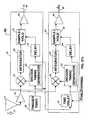
- FIG. 22is a block diagram of a wideband impulse radio transmitter 10 that can be used to implement the vector modulation method of the present invention.
- a precision time base 12provides a periodic timing signal to a time delay modulator 14 .
- the output of time delay modulator 14is coupled to a timing input on a code time modulator 16 .
- the output of the code time modulator 16is coupled to a transmitter output stage 18 .
- the output stage 18generates wideband RF pulses in response to timing signals received from code time modulator 16 .
- the output stage 18is connected to an antenna 20 so that the wideband RF pulses 22 can be emitted and received by a wideband impulse radio receiver.
- FIG. 22depicts the time delay modulator 14 and code time modulator 16 as separate blocks, in alternative embodiments the time delay modulator 14 and code time modulator 16 may be combined together.
- the RF pulses generated by transmitter 10are time modulated by both time delay modulator 14 and code time modulator 16 .
- Code time modulator 16varies the time position of the RF pulses in accordance with a PN code stored in PN code source 24 .
- the PN code sourceis preferably unique to each transmitter so that the PN code can provide channelization, much as a CDMA code does in a conventional spread spectrum radio.
- the time delay modulator 14is responsive to an information source 26 , and provides the time position modulation of the RF pulses that conveys the information (voice and/or data) that needs to be communicated from the transmitter to the receiver.
- the time delay modulator 14is configured to delay each RF pulse by one of four predetermined time delay periods, such as the delays represented in FIGS. 6, 10 , 14 , or 18 .
- One of the four delay periodsis chosen depending on the values of the next two bits of data to be transmitted from information source 26 . For example, if the next two data bits are (1,1), then the delay imposed by time delay modulator 14 to represent this could be chosen to correspond to point M 4 on FIGS. 6 and 7.
- 2 n modulation stateshave to be established by the time delay modulator, and points selected on a correlation of the I and J waveforms that provide an acceptable separation between the modulation states.
- FIG. 23 aOne embodiment of a wideband impulse radio receiver 30 designed to implement such a method is shown in FIG. 23 a .
- the transmitted wideband RF pulses 22are captured by antenna 32 and amplified in an optional wideband RF amplifier 34 .
- the pulsesare then supplied to the inputs of I channel and J channel correlators 36 and 38 .
- each correlator 36 and 38includes a multiplier circuit 40 , each receiving RF pulses from RF amplifier 34 and from a decode timing generator 42 .
- Each decode timing generator 42is operative to generate a sequence of narrow timing pulses corresponding to the PN code used in transmitter 10 (FIG. 22) to time modulate the RF pulses.
- the output of each multiplier 40is a pulse that is integrated by corresponding integrator 44 .
- each integrator 44is connected to the input of a corresponding comparator 46 .
- the second input to each comparatoris connected to a predetermined reference voltage.
- the reference voltagein one embodiment is zero volts for both the I and J comparators 46 .
- the outputs, 56 and 58 , of the I and J comparators 46are indicative of the modulation states imposed on received pulses by the transmitter 10 and thus provide information regarding the two data bits from the transmitter information source 26 associated with the received pulses.
- the decode timing generator 42 in I channel correlator 36is triggered by an adjustable time base 48 that is synchronized to time base 12 in transmitter 10 (FIG. 22) using a signal combiner 50 and loop filter 52 .
- the signal combiner 50 and loop filter 52are connected to the outputs of the integrators 44 and will be described in more detail below.
- Decode timing generator 42 in J channel correlator 38is also triggered by adjustable time base 48 but only after a pre-determined delay period established by adjustable time delay circuit 54 .
- the delay period used for J channel correlator 38is chosen to correspond to points M 1 , M 2 , M 3 , or M 4 on FIG. 6 . This provides an increased amount of separation between the four modulation states.
- an optional summer 43is included between integrators 44 and comparators 46 in both the I and J correlators.
- a predetermined number of multiple pulses having the same modulation stateare transmitted by the transmitter 10 .
- the summers 43 included in the receiver 30sum the outputs of the integrators 44 for the predetermined number of pulses and compare the summed value to a reference voltage using comparators 46 .
- the modulation state associated with the predetermined number of pulsesmay be estimated.
- a predetermined group of multiple pulses having different modulation statesis repeatedly transmitted by the transmitter 10 . Each transmitted group is representative of a single modulation state.
- the summers 43 included in the receiver 30sum the outputs of the integrators 44 for each predetermined group of pulses and compare the summed value to a reference voltage using comparators 46 . As a result, the modulation state associated with each predetermined group of pulses may be estimated.
- each integrator 44is provided to an input on a corresponding track and hold circuit 64 (as shown in FIG. 23 b ).
- Track and hold circuit 64tracks the output of integrator 44 while each received pulse is integrated by the integrator 44 and holds the value output by the integrator 44 after each pulse has been integrated.
- the output of each track and hold circuit 64is a DC voltage that corresponds to the value of a received RF pulse at the end of the tracking period.
- a sample and hold(not shown) may be used in place of the track and hold.
- delay circuits 66After correlation of each RF pulse, delay circuits 66 cause the track and hold circuits to reset.
- delay circuits 66cause the track and hold circuits to reset.
- the outputs of the track and hold circuits 64will indicate the relative time positions of the RF pulses, as modulated by the information component, at a first reference point established by I channel correlator 36 and at a delayed or time offset established by J channel correlator 38 . If the track and hold output of each correlator 36 , 38 is provided to one input of corresponding comparators 46 , with the other comparator inputs connected to ground, then the voltages at I channel output 68 and J channel output 70 will together indicate which of the four modulation states has been imposed on each pulse. That information is representative of two data bits from the transmitter information source 26 (FIG. 22 ).
- the data transmitted by the transmitter 10corresponds to the data 00. If the output of the I correlator is low and the J correlator output is high, the data transmitted by the transmitter 10 is 01. If the I correlator output is high, and the J correlator output is low, the data corresponds to 10. Finally, if the output of both the I and J correlators is low, the transmitted data corresponds to 11.
- FIGS. 23 a and 23 binclude an adjustable time base 48 and a single adjustable time delay circuit 54
- practical hardware limitations inherent in typical time delay circuitsmay require the use of two adjustable time delay circuits in order to achieve the desired delay between the I and J correlators, 36 and 38 .
- the time delay periods necessary between the I and J correlators, 36 and 38may be shorter than the shortest time delay achievable by typical time delay circuits.
- the time delay period achievable by typical time delay circuitsis greater than the time delay needed between the I and J correlators, 36 and 38 .
- 23 a and 23 bmay include an additional adjustable time delay circuit (not shown) connected between the time base 48 and the decode timing generator 42 in the I correlator 36 .
- a controller(not shown) may be used to adjust each of the adjustable time delays to obtain the desired delay between the I and J correlators, 36 and 38 .
- FIG. 24represents the output of a correlator in response to a “real world” pulse received by a receiver 30 after passing through and being distorted by a building wall. Therefore, an actual polar plot of the I and J channel correlator outputs corresponding to varying RF pulse positions may look more like FIG. 25 . This can increase the probability of error by shifting or reducing the separation between the four modulation states. Looking at FIG. 24
- each comparator 46can help correct such error by coupling the second inputs of each comparator 46 to an averaging circuit (not shown).
- Each averaging circuitestablishes a long term average of the value the respective I channel and J channel signals, so that if a DC offset is present, the actual value obtained through integration of each individual RF pulse is compared to the average, rather than to a theoretical zero voltage which would be present if no DC offset was created by a distorted wave shape.
- Another method of compensating for angular skews and DC offsets (as shown for example in FIG. 26) in determining the correct modulation stateis to use linear combinations of the correlator outputs I and J (I+J, I ⁇ J) as shown, for example, in FIGS. 8 and 9, FIGS. 12 and 13, and FIGS. 16 and 17 .
- Another method of compensating for angular and DC offsetsis to use a compensation algorithm that determines an average angle between axis line F and I (FIG. 26) by mapping arctan (J/I) for a number of pulses against a look-up table, then using the average angle and sign ( ⁇ , ⁇ ), ( ⁇ , +), (+, ⁇ ), or (+, +) of the correlator outputs for received pulses.
- the modulation statecan be determined.
- This same angular offset datacan be used to generate an error signal for assisting the receiver in tracking and locking on the received pulses.
- the receiver 30must be able to acquire and maintain lock on the signal transmitted by the transmitter 10 . This is accomplished by synchronizing time base 12 in transmitter 10 with time base 48 in receiver 30 .
- One embodiment for accomplishing the synchronizationincludes a signal combiner 50 and a thresholding circuit (not shown).
- the thresholding circuitcalculates a sum of the absolute value of the outputs of the I and J correlators, 36 and 38 , and, using a comparator (not shown) compares the summed value to a predetermined threshold value.
- the square of the output of the I correlator 36may be summed with the square of the output of the J correlator 38 to generate a summed value for comparison to a predetermined threshold value. In either case, if the summed value is greater than the predetermined threshold value, a signal is generated that engages signal combiner 50 (FIG. 23 a ).
- FIG. 23 cOne embodiment for signal combiner 50 (FIG. 23 a or 23 b ) is shown in FIG. 23 c .
- This embodimentincludes an inverter 76 and a switch 78 .
- the output of the I correlatoris connected to a first input to the switch 78 and an inverted version of the output of the I correlator, generated by passing the output of the I correlator through the inverter 76 , is connected to a second input to the switch 78 .
- the output 58 of the J comparator 46is connected to a third input to the switch 78 .
- the output of the switch 78is connected to the loop filter 52 (FIGS. 23 a and 23 b ) and the output of the loop filter 52 is connected to the adjustable time base 48 .
- the J comparator 46When the output of the J correlator is greater than the reference value, the J comparator 46 generates a signal that causes the switch 78 to pass the output of the I correlator through to the loop filter 52 . When the output of the J correlator falls below the reference value, the J comparator 46 generates a signal that causes the switch 78 to pass the inverted version of the output of the I correlator through to the loop filter 52 . The output of the loop filter 52 is used to adjust the time base 48 until the output of the J correlator rises above the reference value.
- the receiver 30may also include an automatic gain control device to ensure that the lock loop is stable.
- an automatic gain control deviceto ensure that the lock loop is stable.
- AGCautomatic gain control
- the automatic gain control devicestabilizes the lock loop by adjusting the gain of the loop filter to insure that the lock loop operates in a stable manner.
- the automatic gain controllermay be implemented using analog circuits or digital circuits.
- the automatic gain control deviceincludes a pair of signal strength circuits and a magnitude calculation determination circuit (See FIG. 23 A).
- the signal strength circuitsmeasure and feed the absolute value of the outputs of the I and J correlators to the magnitude calculation determination circuit.
- the magnitude calculation determination circuitcompares the absolute value of the I and J correlator outputs to each other and selects the absolute value having the largest magnitude.
- the magnitude calculation determination circuitmay calculate the square root of the sum of the squares of the I and J correlator outputs. In either case, the magnitude calculated by the magnitude calculation determination circuit is inverted and passed to a multiplier 40 . Additional information regarding the automatic gain control device may be found in co-pending U.S. patent application Ser. No. 09/332,501, filed on Jun. 14, 1999, and entitled “System and Method for Impulse Radio Power Control. The disclosure of this patent application is hereby incorporated by reference.
- Another embodiment for acquiring and locking to be used with vector modulationis similar to the QFTM system shown in FIGS. 29 and 30 .
- This methodis based on the observation that when the I correlator is receiving a maximum response, the J correlator is at a null. Since this situation occurs during only one of the four possible data states, it will receive only 1 ⁇ 4 of the total signal energy under ideal balanced conditions where each of the modulation states are statistically equal in occurrence. This is normally not a problem, since the lock loop bandwidth is usually a small fraction of the data bandwidth and will therefore be much more robust than the data channel.
- Whiteningis a process whereby the data is exclusive or-ed with a predetermined pseudo-random sequence to ensure that a long run of ones or zeroes is broken up.
- the whiteningis vulnerable to data having, by chance, the complementary pattern to the sequence and thereby creating a long string of ones or zeroes, but the chance of this is far less than a string of zeroes in the original data, and the probability of such complementary pattern can be made arbitrarily small by lengthening the pseudo-random sequence.
- redundancymay be added to prevent a long string of ones and zeroes. Redundancy in the form of forward error correction works well. Redundancy specifically for guaranteeing lock loop states may be added.
- a cyclic sequence that rotates through all positionsmay be used.
- One such sequenceis 00,10,11,01.
- An additional improvement in the modulation methodis to map the data according to a gray binary code rather than a natural binary code.
- itis important to distinguish between a bin (quadrant) decision error and any bit error resulting therefrom.
- a bin decision errorresults from a condition where a noise voltage overcomes the signal voltage, placing the measured voltage in a different decision bin (quadrant) than the original modulation.
- the resulting data erroris not necessarily 100% wrong. In fact quite a few of the bits (typically approaching 50%) may be the same.
- points M 1 -M 4 of FIG. 9would be assigned 00, 01, 11, 10 respectively rather than 00, 01, 01, 11.
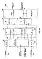
- the receiverhas a first section 80 (FIG. 27 a ) and a digital processor section 82 (FIG. 27 b ).
- the outputs of track and hold circuits 64are coupled to amplifiers 84 , and then to corresponding I channel and J channel A/D converters 86 (FIG. 27 b ).
- the transmitter 10will have four positions (in time) for modulation based on the information component, thus defining four modulation states or quadrants and two bits: (0,0), (0,1), (1,0), and (1,1). Thus one symbol is two bits.
- the code sequence for the channelis 128 bits long, and is divided into four 32-pulse pieces, where each piece represents one symbol. After sending the complete 128-bit cannel code sequence, the transmitter repeats. Therefore, the four unique symbols are sent and continuously repeated.
- the “I” correlator 36fires decode template signal using the same code channel information while the “J” correlator 38 is delayed from the “I” correlator timing by a time offset approximately equal to the time shift that the transmitter 10 uses for its adjacent-symbol time shift.
- the multipliers 40 and integrators 44operate at the pulse level—they function and dump, ready to go again quickly for the next pulse.
- the voltages at each correlator output 88 and 90are digitized after the value of the track and hold circuits 64 settle, and are passed for processing to a processor section that includes a state machine 92 , accumulators 941 and 94 J, and latches 96 and 98 .
- These digital componentscan be integrated in to single device, such as a field programmable gate array (FPGA).
- a code “start” signalis a synchronizing signal from the time base 48 which, in this embodiment, means that the 128-bit channel code sequence is starting at the receiver.
- the state machine 92resets the accumulators 941 and 94 J. It then enables accumulation (integration) for I 1 and J 1 for the first 32 pulses (1 st quadrant, 1 st symbol), then latches the results in latch 96 . Integration stops on (I 1 , J 1 ), then is enabled on (I 2 , J 2 ) for the next 32 pulses and latched. The same process is repeated for (I 3 , J 3 ) and (I 4 , J 4 ), representing 32-pulse integration for modulation quadrants three and four, respectively.
- a vector demodulation algorithm in processor 100plots the signed “I” values along a virtual X-axis, and the signed “J” values along a virtual Y-axis, compares this information to I and J value tables stored in memory 102 , and estimates the value of the two data bits corresponding to each modulation state.
- a delay period of 130 psis used for establishing separation between adjacent modulation states in the transmitter 10 .
- a delay of 130 psis also used between the receiver's “I” and “J” correlator ( 36 , 38 ) triggers (the delay imposed by time delay circuit 54 ).
- the receiverBy use of a phase-locked 1.28 GHz oscillator at the receiver, the receiver is able to slide its correlator triggers in 100 ⁇ 10 ⁇ 9 /32768 seconds per step (or ⁇ 3.052 ps/step) to achieve code phase alignment with the transmitter, as well as to optimally position the “I” channel 36 of into the first modulation state.
- a plot of the scatter points associated with the four modulation statesis shown in FIG. 28 .
- the processor 100can separately monitor the average values of the I and J channel outputs to determine if a DC offset exists that needs correction.
- the processor 100can store a sequence of scatter points generated at the I and J channel outputs 88 and 90 and periodically compare them to an idealized plot of the expected scatter points in each modulation state or quadrant, as stored in memory 102 .
- the processor 100can compensate for error by providing a signal to the J channel timing delay circuit 54 that will vary the amount of delay between triggering of the I and J channel correlators, until separation between the four modulation states is optimized.
- the adjustment of the delay periodcan be communicated to the transmitter as well.
- the processor 100insures that all of the modulation states are equally spaced from each other. To accomplish this, the processor 100 first calculates an average value for each modulation state. Next, the processor 100 calculates the distance between each state. The processor 100 then identifies the minimum distance between any two modulation states and generates an error signal that is used to adjust the time delay circuit 54 , which controls the relative delay between correlators, 36 and 38 . Specifically, the processor 100 adjusts the delay between correlators so that the minimum distance separating any two modulation states is maximized. In an ideal situation, this adjustment process will cause the modulation states to be equally spaced. The delay necessary to maximize the separation may vary according to the propagation path.
- FIG. 28shows a scatter plot of modulation states M 1 , M 2 , M 3 , and M 4 , the modulation states being unequally spaced from each other.
- the processor 100calculates the average value for each modulation state, M 1 avg , M 2 avg , M 3 avg , and M 4 avg .
- the processor 100calculates the distances M 1 avg -M 2 avg , M 2 avg -M 3 avg , M 3 avg -M 4 avg , and M 4 avg -M 1 avg using the averages values of each modulation state.
- the processor 100identifies the two modulation states separated by the shortest distance and generates an error signal that is used to adjust the time delay circuit 54 until the distance is increased as much as possible.
- additional modulation statescan be imposed on transmitted pulses using quadrature flip time modulation (QFTM) wherein a transmitted pulse is delayed and/or inverted in order to impose one or more modulation state, as shown in FIGS. 29 and 30.
- QFTMquadrature flip time modulation
- a first modulation state(representing 0,0) can be defined by pulse that is not delayed and not inverted.
- a second modulation state (0,1)can be defined by a pulse that is delayed but not inverted, and so on.
- FIG. 36 and FIG. 37FIG. 36 is a plot of the I and J correlator outputs, I and J, and an inverted version of the I and J correlator outputs, I (F) and J(F).
- FIG. 37is a polar plot generated by using the correlator outputs shown in FIG. 36 .
- additional modulation statesmay be generated (see M 1 (F) and M 2 (F)).
- FIGS. 38 and 39A similar illustration of this concept is shown in FIGS. 38 and 39. Further information regarding QFTM is disclosed in U.S. patent application Ser. No. 09/537,692, concurrently filed, entitled “Apparatus, System and Method for Flip Modulation in an Impulse Radio Communications System,” which is incorporated herein by reference.
- multiple correlatorsmay be used in the receiver to provide rake acquisition of pulses and additional modulation schemes. By using these additional modulation schemes, increased information about a received pulse can be ascertained, as well as, increased data transfer rates. Further information regarding the use of multiple correlators in a receiver is disclosed in U.S. patent application Ser. No. 09/537,264, concurrently filed with this application, entitled “System and Method of Using Multiple Correlator Receivers in an Impulse Radio System,” which is hereby incorporated into this application by reference.
Landscapes
- Engineering & Computer Science (AREA)
- Computer Networks & Wireless Communication (AREA)
- Signal Processing (AREA)
- Physics & Mathematics (AREA)
- Spectroscopy & Molecular Physics (AREA)
- Digital Transmission Methods That Use Modulated Carrier Waves (AREA)
- Synchronisation In Digital Transmission Systems (AREA)
- Dc Digital Transmission (AREA)
Abstract
Description
Claims (22)
Priority Applications (5)
| Application Number | Priority Date | Filing Date | Title |
|---|---|---|---|
| US09/538,519US6763057B1 (en) | 1999-12-09 | 2000-03-29 | Vector modulation system and method for wideband impulse radio communications |
| JP2001542970AJP2003521143A (en) | 1999-12-09 | 2000-12-08 | Vector modulation system and method for wideband impulse wireless communication |
| AU20732/01AAU2073201A (en) | 1999-12-09 | 2000-12-08 | Vector modulation system and method for wideband impulse radio communications |
| PCT/US2000/033296WO2001043386A1 (en) | 1999-12-09 | 2000-12-08 | Vector modulation system and method for wideband impulse radio communications |
| EP00984053AEP1236327A4 (en) | 1999-12-09 | 2000-12-08 | Vector modulation system and method for wideband impulse radio communications |
Applications Claiming Priority (2)
| Application Number | Priority Date | Filing Date | Title |
|---|---|---|---|
| US16976599P | 1999-12-09 | 1999-12-09 | |
| US09/538,519US6763057B1 (en) | 1999-12-09 | 2000-03-29 | Vector modulation system and method for wideband impulse radio communications |
Publications (1)
| Publication Number | Publication Date |
|---|---|
| US6763057B1true US6763057B1 (en) | 2004-07-13 |
Family
ID=26865357
Family Applications (1)
| Application Number | Title | Priority Date | Filing Date |
|---|---|---|---|
| US09/538,519Expired - Fee RelatedUS6763057B1 (en) | 1999-12-09 | 2000-03-29 | Vector modulation system and method for wideband impulse radio communications |
Country Status (5)
| Country | Link |
|---|---|
| US (1) | US6763057B1 (en) |
| EP (1) | EP1236327A4 (en) |
| JP (1) | JP2003521143A (en) |
| AU (1) | AU2073201A (en) |
| WO (1) | WO2001043386A1 (en) |
Cited By (90)
| Publication number | Priority date | Publication date | Assignee | Title |
|---|---|---|---|---|
| US20030058963A1 (en)* | 2001-09-27 | 2003-03-27 | Stmicroelectronics N.V. | Method and device for decoding an incident pulse signal of the ultra wideband type, in particular for a wireless communication system |
| US20040032354A1 (en)* | 2002-08-16 | 2004-02-19 | Yaron Knobel | Multi-band ultra-wide band communication method and system |
| US20040037282A1 (en)* | 2002-08-22 | 2004-02-26 | Bae Systems Information Electronic Systems Integration, Inc. | Method for real time control of transmit chain for software radios |
| US20040037253A1 (en)* | 2002-08-22 | 2004-02-26 | Bae Systems Information Electronic Systems Integration, Inc. | Method for realtime digital processing of communications signals |
| US20040131130A1 (en)* | 2002-08-16 | 2004-07-08 | Gadi Shor | System and method for multi-band ultra-wide band signal generators |
| US20040146092A1 (en)* | 2003-01-16 | 2004-07-29 | Jaiganesh Balakrishnan | Square-root raised cosine ultra-wideband communications system |
| US20040179580A1 (en)* | 2003-03-10 | 2004-09-16 | Hirohisa Yamaguchi | Spreading code structure for ultra wide band communications |
| US20050129153A1 (en)* | 2000-10-10 | 2005-06-16 | Mccorkle John W. | Ultra wideband communication system, method and device with low noise reception |
| US20050175068A1 (en)* | 2003-02-10 | 2005-08-11 | Yves-Paul Nakache | Randomly changing pulse polarity and phase in an UWB signal for power spectrum density shaping |
| US20050249264A1 (en)* | 2003-02-05 | 2005-11-10 | Nippon Telegraph And Telephone Corpoation | Wireless communication system, wireless transmitter, wireless receiver, wireless communication method, wireless transmission method and wireless reception method |
| US6967993B1 (en)* | 2000-05-26 | 2005-11-22 | Freescale Semiconductor, Inc. | Ultrawide bandwidth system and method for fast synchronization using sub-code spins |
| US20060018369A1 (en)* | 2004-07-23 | 2006-01-26 | Semiconductor Technology Academic Research Center | Impulse-based communication system |
| EP1643656A1 (en)* | 2004-09-30 | 2006-04-05 | Mitsubishi Electric Information Technology Centre Europe B.V. | Interleaved analog-to-digital converting and integrating circuit and telecommunication device comprising such a circuit |
| US20060093021A1 (en)* | 2004-11-03 | 2006-05-04 | Electronics And Telecommunications Research Institute | Code acquisition device and method using two-step search process in DS-CDMA UWB modem |
| US20060093029A1 (en)* | 2004-10-29 | 2006-05-04 | Becker Matthew E | Apparatus and method for grey encoding modulated data |
| US20060275039A1 (en)* | 2005-06-07 | 2006-12-07 | Yuan Chen | Interference-rejection coding method for an optical wireless communication system and the optical wireless communication system thereof |
| US20070053312A1 (en)* | 2005-09-07 | 2007-03-08 | Ran Hay | Pipelined method and apparatus for exchanging information over a wireless network |
| US20070118248A1 (en)* | 2005-11-23 | 2007-05-24 | Samsung Electronics Co., Ltd. | Method and apparatus for reckoning position of moving robot |
| US20070183535A1 (en)* | 2001-03-26 | 2007-08-09 | Irena Maravic | Sampling method for a spread spectrum communication system |
| US20070242026A1 (en)* | 2006-04-14 | 2007-10-18 | Qualcomm Incorporated | Apparatus and method of pulse generation for ultra-wideband transmission |
| US20070248114A1 (en)* | 2006-04-20 | 2007-10-25 | Qualcomm Incorporated | Media access control for ultra-wide band communication |
| US20070259629A1 (en)* | 2006-04-26 | 2007-11-08 | Qualcomm Incorporated | Duty cycling power scheme |
| US20070257827A1 (en)* | 2006-04-20 | 2007-11-08 | Qualcomm Incorporated | Low power output stage |
| US20070279237A1 (en)* | 2006-04-26 | 2007-12-06 | Qualcomm Incorporated | Wireless localization apparatus and method |
| US20070286274A1 (en)* | 2006-04-19 | 2007-12-13 | Qualcomm Incorporated | Apparatus and method of low latency multi-hop communication |
| US20080075153A1 (en)* | 2000-06-12 | 2008-03-27 | Time Domain Corporation | Method and apparatus for applying codes having pre-defined properties |
| US20080112512A1 (en)* | 2006-11-15 | 2008-05-15 | Qualcomm Incorporated | Transmitted reference signaling scheme |
| US20080116941A1 (en)* | 2006-11-16 | 2008-05-22 | Qualcomm Incorporated | Peak signal detector |
| US20080117804A1 (en)* | 2006-11-16 | 2008-05-22 | Qualcomm Incorporated | Multiple access techniques for a wireless communication medium |
| US20080117939A1 (en)* | 2006-11-16 | 2008-05-22 | Qualcomm Incorporated | Multiple access techniques for a wireless communiation medium |
| US20080139127A1 (en)* | 2006-11-08 | 2008-06-12 | Massachusetts Institute Of Technology | Method and apparatus for signal searching |
| US20080144560A1 (en)* | 2006-12-15 | 2008-06-19 | Qualcomm Incorporated | Channel access scheme for ultra-wide band communication |
| US20080183289A1 (en)* | 2007-01-29 | 2008-07-31 | Werblin Research & Development Corp. | Intraocular lens system |
| US20080246548A1 (en)* | 2007-04-05 | 2008-10-09 | Qualcomm Incorporated | Method and apparatus for generating oscillating signals |
| US20080258562A1 (en)* | 2007-04-23 | 2008-10-23 | Qualcomm Incorporated | Apparatus and method for generating fine timing from coarse timing source |
| US20080292022A1 (en)* | 2007-05-21 | 2008-11-27 | Gregory Blum | Radio Receiver Including a Delay-Locked Loop (DLL) for Phase Adjustment |
| US20090017782A1 (en)* | 2007-07-12 | 2009-01-15 | Pavel Monat | Method for determining line-of-sight (los) distance between remote communications devices |
| US20090016548A1 (en)* | 2007-07-10 | 2009-01-15 | Pavel Monat | Super regenerative (sr) apparatus having plurality of parallel sr amplifiers tuned to distinct frequencies |
| US20090021408A1 (en)* | 2007-07-18 | 2009-01-22 | Lee Chong U | Adaptive dynamic range control |
| US20090034591A1 (en)* | 2007-07-30 | 2009-02-05 | David Jonathan Julian | Method of pairing devices |
| US20090061777A1 (en)* | 2007-08-28 | 2009-03-05 | Qualcomm Incorporated | Apparatus and method for modulating an amplitude, phase or both of a periodic signal on a per cycle basis |
| US20090067407A1 (en)* | 2007-09-11 | 2009-03-12 | Qualcomm Incorporated | Keep-alive for wireless networks |
| US20090080542A1 (en)* | 2007-09-25 | 2009-03-26 | Qualcomm Incorporated | Interference Mitigation For Impulse-Based Communication |
| US20090080568A1 (en)* | 2007-09-21 | 2009-03-26 | Qualcomm Incorporated | Signal generator with adjustable phase |
| US20090080101A1 (en)* | 2007-09-21 | 2009-03-26 | Qualcomm Incorporated | Signal generator with adjustable frequency |
| US20090086702A1 (en)* | 2007-09-28 | 2009-04-02 | Qualcomm Incorporated | Randomization of periodic channel scans |
| US20090129441A1 (en)* | 2005-01-28 | 2009-05-21 | Groupe Des Ecoles Des Telecommunications (Get)Institut National Des Telecommunications (Int | UWB Receiver and a Data Transmission Method and System |
| US20090224832A1 (en)* | 2008-03-10 | 2009-09-10 | Qualcomm Incorporated | System and method of enabling a signal processing device in a relatively fast manner to process a low duty cycle signal |
| US20090224860A1 (en)* | 2008-03-10 | 2009-09-10 | Qualcomm Incorporated | System and method of using residual voltage from a prior operation to establish a bias voltage for a subsequent operation |
| US20090243699A1 (en)* | 2008-03-25 | 2009-10-01 | Qualcomm Incorporated | System and method of companding an input signal of an energy detecting receiver |
| US20090251208A1 (en)* | 2008-04-08 | 2009-10-08 | Qualcomm Incorporated | Low power slicer-based demodulator for ppm |
| US20090259672A1 (en)* | 2008-04-15 | 2009-10-15 | Qualcomm Incorporated | Synchronizing timing mismatch by data deletion |
| US20090270030A1 (en)* | 2008-04-23 | 2009-10-29 | Qualcomm Incorporated | Multi-level duty cycling |
| US20090323985A1 (en)* | 2008-06-30 | 2009-12-31 | Qualcomm Incorporated | System and method of controlling power consumption in response to volume control |
| US20100020863A1 (en)* | 2008-07-25 | 2010-01-28 | Qualcomm Incorporated | Determination of receive data values |
| US20100046443A1 (en)* | 2008-08-22 | 2010-02-25 | Qualcomm Incorporated | Addressing schemes for wireless communication |
| US7716001B2 (en) | 2006-11-15 | 2010-05-11 | Qualcomm Incorporated | Delay line calibration |
| US20100150219A1 (en)* | 2008-12-11 | 2010-06-17 | Mi-Kyung Oh | Sampling device and method in wireless communication system |
| US20100157886A1 (en)* | 2007-10-26 | 2010-06-24 | Qualcomm Incorporated | Preamble capture and medium access control |
| US20100172393A1 (en)* | 2009-01-06 | 2010-07-08 | Qualcomm Incorporated | Pulse arbitration for network communications |
| US20100226450A1 (en)* | 2007-10-05 | 2010-09-09 | Nec Corporation | Receiver and wireless communication system equipped with the same |
| US20100241816A1 (en)* | 2009-03-19 | 2010-09-23 | Qualcolmm Incorporated | Optimized transfer of packets in a resource constrained operating environment |
| US7855611B2 (en) | 2006-11-15 | 2010-12-21 | Qualcomm Incorporated | Delay line calibration |
| US7908528B1 (en)* | 2006-10-09 | 2011-03-15 | Altera Corporation | Phase-detector-less method and apparatus for minimizing skew between bonded channel groups |
| US7965805B2 (en) | 2007-09-21 | 2011-06-21 | Qualcomm Incorporated | Signal generator with signal tracking |
| US20110231657A1 (en)* | 2009-03-16 | 2011-09-22 | Qualcomm Incorporated | Apparatus and method for employing codes for telecommunications |
| US20120126869A1 (en)* | 2010-11-18 | 2012-05-24 | Texas Instruments Incorporated | Timing skew error correction apparatus and methods |
| US8351483B1 (en) | 2006-12-18 | 2013-01-08 | University Of South Florida | Architecture for ultra-wideband radio |
| US8375261B2 (en) | 2008-07-07 | 2013-02-12 | Qualcomm Incorporated | System and method of puncturing pulses in a receiver or transmitter |
| US8406794B2 (en) | 2006-04-26 | 2013-03-26 | Qualcomm Incorporated | Methods and apparatuses of initiating communication in wireless networks |
| US8483639B2 (en) | 2008-05-06 | 2013-07-09 | Qualcomm Incorporated | AGC for slicer-based low power demodulator |
| US8514911B2 (en) | 2009-05-13 | 2013-08-20 | Qualcomm Incorporated | Method and apparatus for clock drift compensation during acquisition in a wireless communication system |
| US8538345B2 (en) | 2007-10-09 | 2013-09-17 | Qualcomm Incorporated | Apparatus including housing incorporating a radiating element of an antenna |
| US8552903B2 (en) | 2006-04-18 | 2013-10-08 | Qualcomm Incorporated | Verified distance ranging |
| US8600373B2 (en) | 2006-04-26 | 2013-12-03 | Qualcomm Incorporated | Dynamic distribution of device functionality and resource management |
| US8644396B2 (en) | 2006-04-18 | 2014-02-04 | Qualcomm Incorporated | Waveform encoding for wireless applications |
| US8837724B2 (en) | 2007-03-27 | 2014-09-16 | Qualcomm Incorporated | Synchronization test for device authentication |
| US8886125B2 (en) | 2006-04-14 | 2014-11-11 | Qualcomm Incorporated | Distance-based association |
| US20150110216A1 (en)* | 2012-04-27 | 2015-04-23 | The Royal Institution For The Advancement Of Learning/Mcgill University | Methods and devices for communications systems using multiplied rate transmission |
| US9141961B2 (en) | 2007-06-20 | 2015-09-22 | Qualcomm Incorporated | Management of dynamic mobile coupons |
| US9215581B2 (en) | 2006-04-14 | 2015-12-15 | Qualcomm Incorported | Distance-based presence management |
| US9246725B2 (en)* | 2011-09-06 | 2016-01-26 | Electronics And Telecommunications Research Institute | Method of generating and receiving packets in low energy critical infrastructure monitoring system |
| US9483769B2 (en) | 2007-06-20 | 2016-11-01 | Qualcomm Incorporated | Dynamic electronic coupon for a mobile environment |
| US9524502B2 (en) | 2007-06-20 | 2016-12-20 | Qualcomm Incorporated | Management of dynamic electronic coupons |
| US20180316373A1 (en)* | 2015-10-21 | 2018-11-01 | Tendyron Corporation | Communication device, adapter device, communication system |
| US10542372B2 (en) | 2011-03-15 | 2020-01-21 | Qualcomm Incorporated | User identification within a physical merchant location through the use of a wireless network |
| US20210344531A1 (en)* | 2020-05-04 | 2021-11-04 | Commissariat A L'energie Atomique Et Aux Energies Alternatives | Method for receiving a modulated signal, and associated receiver |
| CN114710209A (en)* | 2022-03-29 | 2022-07-05 | 浙江农林大学 | Encodable information system and method based on vector multiple period soliton pulsation |
| US20220231893A1 (en)* | 2021-01-20 | 2022-07-21 | Uif (University Industry Foundation), Yonsei University | Modulation method, modulation apparatus using the same, demodulation method, and demodulation apparatus using the same |
| US11463231B2 (en)* | 2019-09-13 | 2022-10-04 | Nokomis, Inc | Synchronized multi-channel communication device and method |
Families Citing this family (19)
| Publication number | Priority date | Publication date | Assignee | Title |
|---|---|---|---|---|
| JP4644988B2 (en)* | 2001-07-23 | 2011-03-09 | ソニー株式会社 | Wireless impulse transmitter, receiver and method |
| JP4655429B2 (en)* | 2001-08-01 | 2011-03-23 | ソニー株式会社 | Transmitting apparatus and method thereof, receiving apparatus and method thereof, and communication system and method thereof |
| DE10214113B4 (en) | 2002-03-28 | 2006-05-18 | Siemens Ag | Method for the contactless exchange of a sequence of data bytes in an identification system |
| FR2842974B1 (en)* | 2002-07-26 | 2004-12-03 | Suisse Electronique Microtech | METHOD FOR COMMUNICATING INFORMATION BETWEEN AT LEAST ONE TRANSMITTER AND AT LEAST ONE RECEIVER USING ULTRA-BROADBAND SIGNALS |
| US7764725B2 (en) | 2003-02-14 | 2010-07-27 | Koninklijke Philips Electronics N.V. | Sub-banded ultra-wideband communication system |
| EP1503511A1 (en) | 2003-07-30 | 2005-02-02 | Mitsubishi Electric Information Technology Centre Europe B.V. | Method for detecting UWB pulse sequences and analog detection means suitable for this purpose |
| EP1503513A1 (en)* | 2003-07-30 | 2005-02-02 | Mitsubishi Electric Information Technology Centre Europe B.V. | Method for identifying the beginning of a UWB pulse sequence |
| EP1503512A1 (en)* | 2003-07-30 | 2005-02-02 | Mitsubishi Electric Information Technology Centre Europe B.V. | Method for detecting UWB pulse sequences and detection means suitable for this purpose |
| JP5109668B2 (en)* | 2007-03-09 | 2012-12-26 | セイコーエプソン株式会社 | Receiving apparatus and receiving method |
| JP4408925B2 (en) | 2007-09-28 | 2010-02-03 | 富士通株式会社 | Impulse transmission method, impulse transmission system, transmitter and receiver |
| US8503517B2 (en)* | 2008-06-05 | 2013-08-06 | Qualcomm Incorporated | System and method of an in-band modem for data communications over digital wireless communication networks |
| US8825480B2 (en) | 2008-06-05 | 2014-09-02 | Qualcomm Incorporated | Apparatus and method of obtaining non-speech data embedded in vocoder packet |
| US8964788B2 (en) | 2008-06-05 | 2015-02-24 | Qualcomm Incorporated | System and method of an in-band modem for data communications over digital wireless communication networks |
| US8725502B2 (en) | 2008-06-05 | 2014-05-13 | Qualcomm Incorporated | System and method of an in-band modem for data communications over digital wireless communication networks |
| US9083521B2 (en) | 2008-06-05 | 2015-07-14 | Qualcomm Incorporated | System and method of an in-band modem for data communications over digital wireless communication networks |
| US8743864B2 (en) | 2009-06-16 | 2014-06-03 | Qualcomm Incorporated | System and method for supporting higher-layer protocol messaging in an in-band modem |
| US8855100B2 (en) | 2009-06-16 | 2014-10-07 | Qualcomm Incorporated | System and method for supporting higher-layer protocol messaging in an in-band modem |
| JP5375706B2 (en) | 2010-03-26 | 2013-12-25 | 富士通株式会社 | Wireless communication device |
| CN114650067B (en)* | 2022-03-25 | 2023-03-14 | 清华大学 | Self-synchronizing pulse ultra-wideband signal baseband modulation circuit and demodulation circuit |
Citations (7)
| Publication number | Priority date | Publication date | Assignee | Title |
|---|---|---|---|---|
| US5677927A (en) | 1994-09-20 | 1997-10-14 | Pulson Communications Corporation | Ultrawide-band communication system and method |
| US5812081A (en) | 1984-12-03 | 1998-09-22 | Time Domain Systems, Inc. | Time domain radio transmission system |
| US5832035A (en) | 1994-09-20 | 1998-11-03 | Time Domain Corporation | Fast locking mechanism for channelized ultrawide-band communications |
| US6026125A (en)* | 1997-05-16 | 2000-02-15 | Multispectral Solutions, Inc. | Waveform adaptive ultra-wideband transmitter |
| US6121920A (en) | 1999-05-26 | 2000-09-19 | Barrett; Terence W. | Method and apparatus for enhancing target detection using polarization modulation |
| US6497656B1 (en)* | 2000-02-08 | 2002-12-24 | General Electric Company | Integrated wireless broadband communications network |
| US6504483B1 (en)* | 1998-03-23 | 2003-01-07 | Time Domain Corporation | System and method for using impulse radio technology to track and monitor animals |
- 2000
- 2000-03-29USUS09/538,519patent/US6763057B1/ennot_activeExpired - Fee Related
- 2000-12-08JPJP2001542970Apatent/JP2003521143A/ennot_activeWithdrawn
- 2000-12-08AUAU20732/01Apatent/AU2073201A/ennot_activeAbandoned
- 2000-12-08EPEP00984053Apatent/EP1236327A4/ennot_activeWithdrawn
- 2000-12-08WOPCT/US2000/033296patent/WO2001043386A1/ennot_activeApplication Discontinuation
Patent Citations (7)
| Publication number | Priority date | Publication date | Assignee | Title |
|---|---|---|---|---|
| US5812081A (en) | 1984-12-03 | 1998-09-22 | Time Domain Systems, Inc. | Time domain radio transmission system |
| US5677927A (en) | 1994-09-20 | 1997-10-14 | Pulson Communications Corporation | Ultrawide-band communication system and method |
| US5832035A (en) | 1994-09-20 | 1998-11-03 | Time Domain Corporation | Fast locking mechanism for channelized ultrawide-band communications |
| US6026125A (en)* | 1997-05-16 | 2000-02-15 | Multispectral Solutions, Inc. | Waveform adaptive ultra-wideband transmitter |
| US6504483B1 (en)* | 1998-03-23 | 2003-01-07 | Time Domain Corporation | System and method for using impulse radio technology to track and monitor animals |
| US6121920A (en) | 1999-05-26 | 2000-09-19 | Barrett; Terence W. | Method and apparatus for enhancing target detection using polarization modulation |
| US6497656B1 (en)* | 2000-02-08 | 2002-12-24 | General Electric Company | Integrated wireless broadband communications network |
Non-Patent Citations (3)
| Title |
|---|
| Digital Communications Techniques, Signal Design and Detection, Chapter 3, Scalar and Vector Communications Over the Memoryless Channel, pp. 98-177, Chapter 4, Coherent Communications with Waveforms, pp. 178-292, Marvin K. Simon, et al., Prentice-Hall, Inc., 1995. |
| Paper entitled "Signal Selection for the Indoor Wireless Impulse Radio Channel," Fernando Ramirez-Mireles, et al., Communication Science Institute, Department of Electrical Engineering-Systems, University of Sourthern California, Los Angeles, CA 90089-2565. |
| Spread Spectrum Communications Handbook, Revised Edition, Part 4, Chapter 1, Pseudonoise Code Acquisition in Direct-Sequence Receivers, pp. 751-900, Chapter 2, Pseudocode Tracking in Direct-Sequence Receivers, pp. 901-955, Marvin K. Simon, et al., McGraw-Hill, Inc., 1994. |
Cited By (172)
| Publication number | Priority date | Publication date | Assignee | Title |
|---|---|---|---|---|
| US6967993B1 (en)* | 2000-05-26 | 2005-11-22 | Freescale Semiconductor, Inc. | Ultrawide bandwidth system and method for fast synchronization using sub-code spins |
| US7711026B2 (en)* | 2000-06-12 | 2010-05-04 | Time Domain Corporation | Method and apparatus for applying codes having pre-defined properties |
| US20080075153A1 (en)* | 2000-06-12 | 2008-03-27 | Time Domain Corporation | Method and apparatus for applying codes having pre-defined properties |
| US20050129153A1 (en)* | 2000-10-10 | 2005-06-16 | Mccorkle John W. | Ultra wideband communication system, method and device with low noise reception |
| US7505538B2 (en)* | 2000-10-10 | 2009-03-17 | Freescale Semiconductor, Inc. | Ultra wideband communication system, method and device with low noise reception |
| US8031820B2 (en) | 2001-03-26 | 2011-10-04 | Qualcomm Incorporated | Sampling method, reconstruction method, and device for sampling and/or reconstructing signals |
| US7991095B2 (en) | 2001-03-26 | 2011-08-02 | Qualcomm Incorporated | Sampling method, reconstruction method, and device for sampling and/or reconstructing signals |
| US8077757B2 (en) | 2001-03-26 | 2011-12-13 | Qualcomm Incorporated | Sampling method for a spread spectrum communication system |
| US20100246729A1 (en)* | 2001-03-26 | 2010-09-30 | Qualcomm Incorporated | Sampling method, reconstruction method, and device for sampling and/or reconstructing signals |
| US8160194B2 (en) | 2001-03-26 | 2012-04-17 | Qualcomm Incorporated | Sampling method, reconstruction method, and device for sampling and/or reconstructing signals |
| US20070183535A1 (en)* | 2001-03-26 | 2007-08-09 | Irena Maravic | Sampling method for a spread spectrum communication system |
| US20030058963A1 (en)* | 2001-09-27 | 2003-03-27 | Stmicroelectronics N.V. | Method and device for decoding an incident pulse signal of the ultra wideband type, in particular for a wireless communication system |
| US7054349B2 (en)* | 2001-09-27 | 2006-05-30 | Stmicroelectronics N.V. | Method and device for decoding an incident pulse signal of the ultra wideband type, in particular for a wireless communication system |
| US20040131130A1 (en)* | 2002-08-16 | 2004-07-08 | Gadi Shor | System and method for multi-band ultra-wide band signal generators |
| US7539271B2 (en)* | 2002-08-16 | 2009-05-26 | Wisair Ltd. | System and method for multi-band ultra-wide band signal generators |
| US7221911B2 (en)* | 2002-08-16 | 2007-05-22 | Wisair Ltd. | Multi-band ultra-wide band communication method and system |
| US20040032354A1 (en)* | 2002-08-16 | 2004-02-19 | Yaron Knobel | Multi-band ultra-wide band communication method and system |
| US7573863B2 (en)* | 2002-08-22 | 2009-08-11 | Bae Systems Information And Electronic Systems Integration Inc. | Method for real time control of transmit chain for software radios |
| US7573864B2 (en)* | 2002-08-22 | 2009-08-11 | Bae Systems Information And Electronic Systems Integration Inc. | Method for realtime digital processing of communications signals |
| US20090238166A1 (en)* | 2002-08-22 | 2009-09-24 | Boland Robert P | Method for realtime digital processing of communications signals |
| US20040037253A1 (en)* | 2002-08-22 | 2004-02-26 | Bae Systems Information Electronic Systems Integration, Inc. | Method for realtime digital processing of communications signals |
| US20040037282A1 (en)* | 2002-08-22 | 2004-02-26 | Bae Systems Information Electronic Systems Integration, Inc. | Method for real time control of transmit chain for software radios |
| US7440491B2 (en)* | 2003-01-16 | 2008-10-21 | Texas Instruments Incorporated | Ultra-wideband communications system devices |
| US20040146092A1 (en)* | 2003-01-16 | 2004-07-29 | Jaiganesh Balakrishnan | Square-root raised cosine ultra-wideband communications system |
| US7545845B2 (en)* | 2003-02-05 | 2009-06-09 | Nippon Telegraph And Telephone Corporation | Wireless communication system, wireless transmitter, wireless receiver, wireless communication method, wireless transmission method and wireless reception method |
| US20050249264A1 (en)* | 2003-02-05 | 2005-11-10 | Nippon Telegraph And Telephone Corpoation | Wireless communication system, wireless transmitter, wireless receiver, wireless communication method, wireless transmission method and wireless reception method |
| US20050175068A1 (en)* | 2003-02-10 | 2005-08-11 | Yves-Paul Nakache | Randomly changing pulse polarity and phase in an UWB signal for power spectrum density shaping |
| US7298792B2 (en)* | 2003-02-10 | 2007-11-20 | Mitsubishi Electric Research Laboratories, Inc. | Randomly changing pulse polarity and phase in an UWB signal for power spectrum density shaping |
| US7388899B2 (en)* | 2003-03-10 | 2008-06-17 | Texas Instruments Incorporated | Spreading code structure for ultra wide band communications |
| US20040179580A1 (en)* | 2003-03-10 | 2004-09-16 | Hirohisa Yamaguchi | Spreading code structure for ultra wide band communications |
| US7590198B2 (en)* | 2004-07-23 | 2009-09-15 | Semiconductor Technology Academic Research Center | Impulse-based communication system |
| US20060018369A1 (en)* | 2004-07-23 | 2006-01-26 | Semiconductor Technology Academic Research Center | Impulse-based communication system |
| EP1643656A1 (en)* | 2004-09-30 | 2006-04-05 | Mitsubishi Electric Information Technology Centre Europe B.V. | Interleaved analog-to-digital converting and integrating circuit and telecommunication device comprising such a circuit |
| US20060093029A1 (en)* | 2004-10-29 | 2006-05-04 | Becker Matthew E | Apparatus and method for grey encoding modulated data |
| US7382822B2 (en)* | 2004-11-03 | 2008-06-03 | Electronics And Telecommunications Research Institute | Code acquisition device and method using two-step search process in DS-CDMA UWB modem |
| US20060093021A1 (en)* | 2004-11-03 | 2006-05-04 | Electronics And Telecommunications Research Institute | Code acquisition device and method using two-step search process in DS-CDMA UWB modem |
| US8355425B2 (en) | 2005-01-28 | 2013-01-15 | Groupe Des Ecoles Des Telecommunications (Get) Institut National Des Telecommunications (Int) | UWB receiver and a data transmission method and system |
| US20090129441A1 (en)* | 2005-01-28 | 2009-05-21 | Groupe Des Ecoles Des Telecommunications (Get)Institut National Des Telecommunications (Int | UWB Receiver and a Data Transmission Method and System |
| US20060275039A1 (en)* | 2005-06-07 | 2006-12-07 | Yuan Chen | Interference-rejection coding method for an optical wireless communication system and the optical wireless communication system thereof |
| US7689132B2 (en)* | 2005-06-07 | 2010-03-30 | Industrial Technology Research Institute | Interference-rejection coding method for an optical wireless communication system and the optical wireless communication system thereof |
| US20100074627A1 (en)* | 2005-06-07 | 2010-03-25 | Yuan Chen | Interference-Rejection Coding Method For An Optical Wireless Communication System And The Optical Wireless Communication System Thereof |
| US20070053312A1 (en)* | 2005-09-07 | 2007-03-08 | Ran Hay | Pipelined method and apparatus for exchanging information over a wireless network |
| US9058039B2 (en)* | 2005-11-23 | 2015-06-16 | Samsung Electronics Co., Ltd. | Method and apparatus for reckoning position of moving robot |
| US20070118248A1 (en)* | 2005-11-23 | 2007-05-24 | Samsung Electronics Co., Ltd. | Method and apparatus for reckoning position of moving robot |
| US9591470B2 (en) | 2006-04-14 | 2017-03-07 | Qualcomm Incorporated | System and method for enabling operations based on distance to and motion of remote device |
| US9510383B2 (en) | 2006-04-14 | 2016-11-29 | Qualcomm Incorporated | System and method of associating devices based on actuation of input devices and signal strength |
| US9215581B2 (en) | 2006-04-14 | 2015-12-15 | Qualcomm Incorported | Distance-based presence management |
| US8886125B2 (en) | 2006-04-14 | 2014-11-11 | Qualcomm Incorporated | Distance-based association |
| US20070242026A1 (en)* | 2006-04-14 | 2007-10-18 | Qualcomm Incorporated | Apparatus and method of pulse generation for ultra-wideband transmission |
| US8644396B2 (en) | 2006-04-18 | 2014-02-04 | Qualcomm Incorporated | Waveform encoding for wireless applications |
| US8654868B2 (en) | 2006-04-18 | 2014-02-18 | Qualcomm Incorporated | Offloaded processing for wireless applications |
| US8552903B2 (en) | 2006-04-18 | 2013-10-08 | Qualcomm Incorporated | Verified distance ranging |
| US20070286274A1 (en)* | 2006-04-19 | 2007-12-13 | Qualcomm Incorporated | Apparatus and method of low latency multi-hop communication |
| US8811456B2 (en) | 2006-04-19 | 2014-08-19 | Qualcomm Incorporated | Apparatus and method of low latency multi-hop communication |
| US20070257827A1 (en)* | 2006-04-20 | 2007-11-08 | Qualcomm Incorporated | Low power output stage |
| US9124357B2 (en) | 2006-04-20 | 2015-09-01 | Qualcomm Incorporated | Media access control for ultra-wide band communication |
| US20070248114A1 (en)* | 2006-04-20 | 2007-10-25 | Qualcomm Incorporated | Media access control for ultra-wide band communication |
| US7576605B2 (en) | 2006-04-20 | 2009-08-18 | Qualcomm Incorporated | Low power output stage |
| US20070279237A1 (en)* | 2006-04-26 | 2007-12-06 | Qualcomm Incorporated | Wireless localization apparatus and method |
| US8553745B2 (en) | 2006-04-26 | 2013-10-08 | Qualcomm Incorporated | Inter-pulse duty cycling |
| US20070259629A1 (en)* | 2006-04-26 | 2007-11-08 | Qualcomm Incorporated | Duty cycling power scheme |
| US20070258507A1 (en)* | 2006-04-26 | 2007-11-08 | Qualcomm Incorporated | Inter-pulse duty cycling |
| US8600373B2 (en) | 2006-04-26 | 2013-12-03 | Qualcomm Incorporated | Dynamic distribution of device functionality and resource management |
| US20070259662A1 (en)* | 2006-04-26 | 2007-11-08 | Qualcomm Incorporated | Wireless device communication with multiple peripherals |
| US8289159B2 (en) | 2006-04-26 | 2012-10-16 | Qualcomm Incorporated | Wireless localization apparatus and method |
| US20070291684A1 (en)* | 2006-04-26 | 2007-12-20 | Qualcomm Incorporated | Sub-packet pulse-based communications |
| US8406794B2 (en) | 2006-04-26 | 2013-03-26 | Qualcomm Incorporated | Methods and apparatuses of initiating communication in wireless networks |
| US8451710B2 (en) | 2006-04-26 | 2013-05-28 | Qualcomm Incorporated | Sub-packet pulse-based communications |
| US8527016B2 (en) | 2006-04-26 | 2013-09-03 | Qualcomm Incorporated | Wireless device communication with multiple peripherals |
| US7908528B1 (en)* | 2006-10-09 | 2011-03-15 | Altera Corporation | Phase-detector-less method and apparatus for minimizing skew between bonded channel groups |
| US20080139127A1 (en)* | 2006-11-08 | 2008-06-12 | Massachusetts Institute Of Technology | Method and apparatus for signal searching |
| US8565690B2 (en)* | 2006-11-08 | 2013-10-22 | Massachusetts Institute Of Technology | Method and apparatus for signal searching |
| US20080112512A1 (en)* | 2006-11-15 | 2008-05-15 | Qualcomm Incorporated | Transmitted reference signaling scheme |
| US7855611B2 (en) | 2006-11-15 | 2010-12-21 | Qualcomm Incorporated | Delay line calibration |
| US20110080203A1 (en)* | 2006-11-15 | 2011-04-07 | Qualcomm Incorporated | Delay line calibration |
| US8698572B2 (en) | 2006-11-15 | 2014-04-15 | Qualcomm Incorporated | Delay line calibration |
| US7716001B2 (en) | 2006-11-15 | 2010-05-11 | Qualcomm Incorporated | Delay line calibration |
| US20080116941A1 (en)* | 2006-11-16 | 2008-05-22 | Qualcomm Incorporated | Peak signal detector |
| US20080117804A1 (en)* | 2006-11-16 | 2008-05-22 | Qualcomm Incorporated | Multiple access techniques for a wireless communication medium |
| US8014425B2 (en) | 2006-11-16 | 2011-09-06 | Qualcomm Incorporated | Multiple access techniques for a wireless communiation medium |
| US7889753B2 (en) | 2006-11-16 | 2011-02-15 | Qualcomm Incorporated | Multiple access techniques for a wireless communication medium |
| US20080117939A1 (en)* | 2006-11-16 | 2008-05-22 | Qualcomm Incorporated | Multiple access techniques for a wireless communiation medium |
| US20080144560A1 (en)* | 2006-12-15 | 2008-06-19 | Qualcomm Incorporated | Channel access scheme for ultra-wide band communication |
| US8363583B2 (en) | 2006-12-15 | 2013-01-29 | Qualcomm Incorporated | Channel access scheme for ultra-wide band communication |
| US8724677B1 (en) | 2006-12-18 | 2014-05-13 | University Of South Florida | Architecture for ultra-wideband radio |
| US8588270B1 (en) | 2006-12-18 | 2013-11-19 | University Of South Florida | Architecture for ultra-wideband radio |
| US8351483B1 (en) | 2006-12-18 | 2013-01-08 | University Of South Florida | Architecture for ultra-wideband radio |
| US20080183289A1 (en)* | 2007-01-29 | 2008-07-31 | Werblin Research & Development Corp. | Intraocular lens system |
| US8837724B2 (en) | 2007-03-27 | 2014-09-16 | Qualcomm Incorporated | Synchronization test for device authentication |
| US7592878B2 (en) | 2007-04-05 | 2009-09-22 | Qualcomm Incorporated | Method and apparatus for generating oscillating signals |
| US7902936B2 (en) | 2007-04-05 | 2011-03-08 | Qualcomm Incorporated | Method and apparatus for generating oscillating signals |
| US20080246548A1 (en)* | 2007-04-05 | 2008-10-09 | Qualcomm Incorporated | Method and apparatus for generating oscillating signals |
| US7834482B2 (en) | 2007-04-23 | 2010-11-16 | Qualcomm Incorporated | Apparatus and method for generating fine timing from coarse timing source |
| US20080258562A1 (en)* | 2007-04-23 | 2008-10-23 | Qualcomm Incorporated | Apparatus and method for generating fine timing from coarse timing source |
| US7817750B2 (en) | 2007-05-21 | 2010-10-19 | Seiko Epson Corporation | Radio receiver including a delay-locked loop (DLL) for phase adjustment |
| US20080292022A1 (en)* | 2007-05-21 | 2008-11-27 | Gregory Blum | Radio Receiver Including a Delay-Locked Loop (DLL) for Phase Adjustment |
| US9141961B2 (en) | 2007-06-20 | 2015-09-22 | Qualcomm Incorporated | Management of dynamic mobile coupons |
| US9483769B2 (en) | 2007-06-20 | 2016-11-01 | Qualcomm Incorporated | Dynamic electronic coupon for a mobile environment |
| US9747613B2 (en) | 2007-06-20 | 2017-08-29 | Qualcomm Incorporated | Dynamic electronic coupon for a mobile environment |
| US9524502B2 (en) | 2007-06-20 | 2016-12-20 | Qualcomm Incorporated | Management of dynamic electronic coupons |
| US20090016548A1 (en)* | 2007-07-10 | 2009-01-15 | Pavel Monat | Super regenerative (sr) apparatus having plurality of parallel sr amplifiers tuned to distinct frequencies |
| US8326246B2 (en) | 2007-07-10 | 2012-12-04 | Qualcomm Incorporated | Super regenerative (SR) apparatus having plurality of parallel SR amplifiers tuned to distinct frequencies |
| US20090017782A1 (en)* | 2007-07-12 | 2009-01-15 | Pavel Monat | Method for determining line-of-sight (los) distance between remote communications devices |
| US8103228B2 (en) | 2007-07-12 | 2012-01-24 | Qualcomm Incorporated | Method for determining line-of-sight (LOS) distance between remote communications devices |
| US20090021408A1 (en)* | 2007-07-18 | 2009-01-22 | Lee Chong U | Adaptive dynamic range control |
| US7576672B2 (en) | 2007-07-18 | 2009-08-18 | Qualcomm Incorporated | Adaptive Dynamic Range Control |
| US8059573B2 (en) | 2007-07-30 | 2011-11-15 | Qualcomm Incorporated | Method of pairing devices |
| US20090034591A1 (en)* | 2007-07-30 | 2009-02-05 | David Jonathan Julian | Method of pairing devices |
| US20090061777A1 (en)* | 2007-08-28 | 2009-03-05 | Qualcomm Incorporated | Apparatus and method for modulating an amplitude, phase or both of a periodic signal on a per cycle basis |
| US8406693B2 (en) | 2007-08-28 | 2013-03-26 | Qualcomm Incorporated | Apparatus and method for modulating an amplitude, phase or both of a periodic signal on a per cycle basis |
| US20110129099A1 (en)* | 2007-08-28 | 2011-06-02 | Qualcomm Incorporated | Apparatus and method for modulating an amplitude, phase or both of a periodic signal on a per cycle basis |
| US7974580B2 (en) | 2007-08-28 | 2011-07-05 | Qualcomm Incorporated | Apparatus and method for modulating an amplitude, phase or both of a periodic signal on a per cycle basis |
| US8005065B2 (en) | 2007-09-11 | 2011-08-23 | Qualcomm Incorporated | Keep-alive for wireless networks |
| US20090067407A1 (en)* | 2007-09-11 | 2009-03-12 | Qualcomm Incorporated | Keep-alive for wireless networks |
| US8446976B2 (en) | 2007-09-21 | 2013-05-21 | Qualcomm Incorporated | Signal generator with adjustable phase |
| US7965805B2 (en) | 2007-09-21 | 2011-06-21 | Qualcomm Incorporated | Signal generator with signal tracking |
| US20090080568A1 (en)* | 2007-09-21 | 2009-03-26 | Qualcomm Incorporated | Signal generator with adjustable phase |
| US8385474B2 (en) | 2007-09-21 | 2013-02-26 | Qualcomm Incorporated | Signal generator with adjustable frequency |
| US20090080101A1 (en)* | 2007-09-21 | 2009-03-26 | Qualcomm Incorporated | Signal generator with adjustable frequency |
| US8233572B2 (en) | 2007-09-25 | 2012-07-31 | Qualcomm Incorporated | Interference mitigation for impulse-based communication |
| US20090080542A1 (en)* | 2007-09-25 | 2009-03-26 | Qualcomm Incorporated | Interference Mitigation For Impulse-Based Communication |
| US20090086702A1 (en)* | 2007-09-28 | 2009-04-02 | Qualcomm Incorporated | Randomization of periodic channel scans |
| US8275373B2 (en) | 2007-09-28 | 2012-09-25 | Qualcomm Incorporated | Randomization of periodic channel scans |
| US8340223B2 (en)* | 2007-10-05 | 2012-12-25 | Nec Corporation | Receiver and wireless communication system equipped with the same |
| US20100226450A1 (en)* | 2007-10-05 | 2010-09-09 | Nec Corporation | Receiver and wireless communication system equipped with the same |
| US8538345B2 (en) | 2007-10-09 | 2013-09-17 | Qualcomm Incorporated | Apparatus including housing incorporating a radiating element of an antenna |
| US20100157886A1 (en)* | 2007-10-26 | 2010-06-24 | Qualcomm Incorporated | Preamble capture and medium access control |
| US9083448B2 (en) | 2007-10-26 | 2015-07-14 | Qualcomm Incorporated | Preamble capture and medium access control |
| US8275343B2 (en) | 2008-03-10 | 2012-09-25 | Qualcomm Incorporated | System and method of using residual voltage from a prior operation to establish a bias voltage for a subsequent operation |
| US20090224860A1 (en)* | 2008-03-10 | 2009-09-10 | Qualcomm Incorporated | System and method of using residual voltage from a prior operation to establish a bias voltage for a subsequent operation |
| US20090224832A1 (en)* | 2008-03-10 | 2009-09-10 | Qualcomm Incorporated | System and method of enabling a signal processing device in a relatively fast manner to process a low duty cycle signal |
| US7812667B2 (en) | 2008-03-10 | 2010-10-12 | Qualcomm Incorporated | System and method of enabling a signal processing device in a relatively fast manner to process a low duty cycle signal |
| US8254595B2 (en) | 2008-03-25 | 2012-08-28 | Qualcomm Incorporated | System and method of companding an input signal of an energy detecting receiver |
| US20090243699A1 (en)* | 2008-03-25 | 2009-10-01 | Qualcomm Incorporated | System and method of companding an input signal of an energy detecting receiver |
| US7868689B2 (en) | 2008-04-08 | 2011-01-11 | Qualcomm Incorporated | Low power slicer-based demodulator for PPM |
| US20090251208A1 (en)* | 2008-04-08 | 2009-10-08 | Qualcomm Incorporated | Low power slicer-based demodulator for ppm |
| US20090259671A1 (en)* | 2008-04-15 | 2009-10-15 | Qualcomm Incorporated | Synchronizing timing mismatch by data insertion |
| US20090259672A1 (en)* | 2008-04-15 | 2009-10-15 | Qualcomm Incorporated | Synchronizing timing mismatch by data deletion |
| US8589720B2 (en) | 2008-04-15 | 2013-11-19 | Qualcomm Incorporated | Synchronizing timing mismatch by data insertion |
| US20090270030A1 (en)* | 2008-04-23 | 2009-10-29 | Qualcomm Incorporated | Multi-level duty cycling |
| US8473013B2 (en) | 2008-04-23 | 2013-06-25 | Qualcomm Incorporated | Multi-level duty cycling |
| US8483639B2 (en) | 2008-05-06 | 2013-07-09 | Qualcomm Incorporated | AGC for slicer-based low power demodulator |
| US20090323985A1 (en)* | 2008-06-30 | 2009-12-31 | Qualcomm Incorporated | System and method of controlling power consumption in response to volume control |
| US8375261B2 (en) | 2008-07-07 | 2013-02-12 | Qualcomm Incorporated | System and method of puncturing pulses in a receiver or transmitter |
| US20100020863A1 (en)* | 2008-07-25 | 2010-01-28 | Qualcomm Incorporated | Determination of receive data values |
| US8787440B2 (en) | 2008-07-25 | 2014-07-22 | Qualcomm Incorporated | Determination of receive data values |
| US8848636B2 (en) | 2008-08-22 | 2014-09-30 | Qualcomm Incorporated | Addressing schemes for wireless communication |
| US8165080B2 (en) | 2008-08-22 | 2012-04-24 | Qualcomm Incorporated | Addressing schemes for wireless communication |
| US20100046443A1 (en)* | 2008-08-22 | 2010-02-25 | Qualcomm Incorporated | Addressing schemes for wireless communication |
| US20100150219A1 (en)* | 2008-12-11 | 2010-06-17 | Mi-Kyung Oh | Sampling device and method in wireless communication system |
| US8553744B2 (en) | 2009-01-06 | 2013-10-08 | Qualcomm Incorporated | Pulse arbitration for network communications |
| US20100172393A1 (en)* | 2009-01-06 | 2010-07-08 | Qualcomm Incorporated | Pulse arbitration for network communications |
| US20110231657A1 (en)* | 2009-03-16 | 2011-09-22 | Qualcomm Incorporated | Apparatus and method for employing codes for telecommunications |
| US8612693B2 (en) | 2009-03-19 | 2013-12-17 | Qualcomm Incorporated | Optimized transfer of packets in a resource constrained operating environment |
| US20100241816A1 (en)* | 2009-03-19 | 2010-09-23 | Qualcolmm Incorporated | Optimized transfer of packets in a resource constrained operating environment |
| US8514911B2 (en) | 2009-05-13 | 2013-08-20 | Qualcomm Incorporated | Method and apparatus for clock drift compensation during acquisition in a wireless communication system |
| US8269528B2 (en)* | 2010-11-18 | 2012-09-18 | Texas Instruments Incorporated | Timing skew error correction apparatus and methods |
| US20120126869A1 (en)* | 2010-11-18 | 2012-05-24 | Texas Instruments Incorporated | Timing skew error correction apparatus and methods |
| US10542372B2 (en) | 2011-03-15 | 2020-01-21 | Qualcomm Incorporated | User identification within a physical merchant location through the use of a wireless network |
| US9246725B2 (en)* | 2011-09-06 | 2016-01-26 | Electronics And Telecommunications Research Institute | Method of generating and receiving packets in low energy critical infrastructure monitoring system |
| US9473332B2 (en)* | 2012-04-27 | 2016-10-18 | The Royal Institution For The Advancement Of Learning / Mcgill University | Methods and devices for communications systems using multiplied rate transmission |
| US20150110216A1 (en)* | 2012-04-27 | 2015-04-23 | The Royal Institution For The Advancement Of Learning/Mcgill University | Methods and devices for communications systems using multiplied rate transmission |
| US20180316373A1 (en)* | 2015-10-21 | 2018-11-01 | Tendyron Corporation | Communication device, adapter device, communication system |
| US10673477B2 (en)* | 2015-10-21 | 2020-06-02 | Tendyron Corporation | Communication device, adapter device, communication system |
| US11463231B2 (en)* | 2019-09-13 | 2022-10-04 | Nokomis, Inc | Synchronized multi-channel communication device and method |
| US11936766B2 (en) | 2019-09-13 | 2024-03-19 | Nokomis, Inc. | Direct conversion receiver using coherent integration |
| US11477062B2 (en)* | 2020-05-04 | 2022-10-18 | Commissariat A L'energie Atomique Et Aux Energies Alternatives | Method for receiving a modulated signal, and associated receiver |
| US20210344531A1 (en)* | 2020-05-04 | 2021-11-04 | Commissariat A L'energie Atomique Et Aux Energies Alternatives | Method for receiving a modulated signal, and associated receiver |
| US20220231893A1 (en)* | 2021-01-20 | 2022-07-21 | Uif (University Industry Foundation), Yonsei University | Modulation method, modulation apparatus using the same, demodulation method, and demodulation apparatus using the same |
| US11881974B2 (en)* | 2021-01-20 | 2024-01-23 | Uif (University Industry Foundation), Yonsei University | Modulation method, modulation apparatus using the same, demodulation method, and demodulation apparatus using the same |
| CN114710209A (en)* | 2022-03-29 | 2022-07-05 | 浙江农林大学 | Encodable information system and method based on vector multiple period soliton pulsation |
| CN114710209B (en)* | 2022-03-29 | 2024-02-13 | 浙江农林大学 | A codable information system and method based on vector period-doubling soliton pulsation |
Also Published As
| Publication number | Publication date |
|---|---|
| AU2073201A (en) | 2001-06-18 |
| EP1236327A1 (en) | 2002-09-04 |
| JP2003521143A (en) | 2003-07-08 |
| EP1236327A4 (en) | 2003-07-23 |
| WO2001043386A1 (en) | 2001-06-14 |
Similar Documents
| Publication | Publication Date | Title |
|---|---|---|
| US6763057B1 (en) | Vector modulation system and method for wideband impulse radio communications | |
| US7508865B2 (en) | System and method for tracking an ultrawide bandwidth signal | |
| US7526250B2 (en) | Apparatus, system and method for flip modulation in an impulse radio communications system | |
| US5960031A (en) | Ultrawide-band communication system and method | |
| US7280615B2 (en) | Method for making a clear channel assessment in a wireless network | |
| US6717992B2 (en) | Method and apparatus for receiving a plurality of time spaced signals | |
| US7903778B2 (en) | Low power, high resolution timing generator for ultra-wide bandwidth communication systems | |
| US6954480B2 (en) | Method and apparatus for improving received signal quality in an impulse radio system | |
| US20020075972A1 (en) | Apparatus, system and method for one-of-many positions modulation in an impulse radio communications system | |
| WO2001093446A2 (en) | Ultrawide bandwidth communication system and method for fast synchronisation | |
| US7194019B2 (en) | Multi-pulse multi-delay (MPMD) multiple access modulation for UWB | |
| US8743927B2 (en) | Low power, high resolution timing generator for ultra-wide bandwidth communication systems | |
| WO2001093442A1 (en) | Ultrawide band system and method for fast synchronization using multiple detection arms | |
| Moragrega et al. | Ultra-wideband testbed for 6.0–8.5 GHz ranging and low data rate communication | |
| Sahukar et al. | Progress in Development of Differential Code Shift Reference Impulse Radio Ultra Wideband Transceiver | |
| WO2001095508A2 (en) | Apparatus and method for pulse position modulation in an impulse radio communications system | |
| Krebesz et al. | A new, near-coherent detector configuration for UWB impulse radio | |
| AU1493400A (en) | An impulse radio communication apparatus |
Legal Events
| Date | Code | Title | Description |
|---|---|---|---|
| AS | Assignment | Owner name:TIME DOMAIN CORPORATION, ALABAMA Free format text:ASSIGNMENT OF ASSIGNORS INTEREST;ASSIGNORS:FULLERTON, LARRY W.;RICHARDS, JAMES L.;COWIE, IVAN A.;AND OTHERS;REEL/FRAME:014099/0360 Effective date:20030520 | |
| FEPP | Fee payment procedure | Free format text:PAYOR NUMBER ASSIGNED (ORIGINAL EVENT CODE: ASPN); ENTITY STATUS OF PATENT OWNER: LARGE ENTITY | |
| REMI | Maintenance fee reminder mailed | ||
| FPAY | Fee payment | Year of fee payment:4 | |
| SULP | Surcharge for late payment | ||
| FEPP | Fee payment procedure | Free format text:PAT HOLDER NO LONGER CLAIMS SMALL ENTITY STATUS, ENTITY STATUS SET TO UNDISCOUNTED (ORIGINAL EVENT CODE: STOL); ENTITY STATUS OF PATENT OWNER: LARGE ENTITY | |
| AS | Assignment | Owner name:ALEREON, INC., TEXAS Free format text:ASSIGNMENT OF ASSIGNORS INTEREST;ASSIGNOR:TIME DOMAIN CORPORATION;REEL/FRAME:026603/0248 Effective date:20090521 | |
| FPAY | Fee payment | Year of fee payment:8 | |
| AS | Assignment | Owner name:ALEREON, INC., TEXAS Free format text:RELEASE BY SECURED PARTY;ASSIGNOR:VENTURE LENDING & LEASING V, INC.;REEL/FRAME:027982/0868 Effective date:20120330 Owner name:ALEREON, INC., TEXAS Free format text:RELEASE BY SECURED PARTY;ASSIGNOR:VENTURE LENDING & LEASING IV, INC.;REEL/FRAME:027982/0814 Effective date:20120330 | |
| AS | Assignment | Owner name:ENHANCED JOBS FOR TEXAS FUND, LLC, NEW YORK Free format text:SECURITY AGREEMENT;ASSIGNOR:ALEREON, INC.;REEL/FRAME:028039/0323 Effective date:20120412 Owner name:ENHANCED CAPITAL TEXAS FUND II, LLC, NEW YORK Free format text:SECURITY AGREEMENT;ASSIGNOR:ALEREON, INC.;REEL/FRAME:028039/0323 Effective date:20120412 | |
| AS | Assignment | Owner name:ENHANCED CREDIT SUPPORTED LOAN FUND, LP, NEW YORK Free format text:SECURITY AGREEMENT;ASSIGNOR:ALEREON, INC.;REEL/FRAME:031948/0386 Effective date:20131227 Owner name:ALEREON, INC., TEXAS Free format text:RELEASE BY SECURED PARTY;ASSIGNORS:ENHANCED CAPITAL TEXAS FUND II, LLC;ENHANCED JOBS FOR TEXAS FUND, LLC;REEL/FRAME:031948/0065 Effective date:20131227 | |
| REMI | Maintenance fee reminder mailed | ||
| LAPS | Lapse for failure to pay maintenance fees | ||
| STCH | Information on status: patent discontinuation | Free format text:PATENT EXPIRED DUE TO NONPAYMENT OF MAINTENANCE FEES UNDER 37 CFR 1.362 | |
| FP | Lapsed due to failure to pay maintenance fee | Effective date:20160713 |