US6762483B1 - Narrow fin FinFET - Google Patents
Narrow fin FinFETDownload PDFInfo
- Publication number
- US6762483B1 US6762483B1US10/348,910US34891003AUS6762483B1US 6762483 B1US6762483 B1US 6762483B1US 34891003 AUS34891003 AUS 34891003AUS 6762483 B1US6762483 B1US 6762483B1
- Authority
- US
- United States
- Prior art keywords
- layer
- fin structure
- double
- gate
- forming
- Prior art date
- Legal status (The legal status is an assumption and is not a legal conclusion. Google has not performed a legal analysis and makes no representation as to the accuracy of the status listed.)
- Expired - Lifetime
Links
- 238000000034methodMethods0.000claimsabstractdescription35
- 238000000151depositionMethods0.000claimsdescription10
- 238000005530etchingMethods0.000claimsdescription8
- 229910021420polycrystalline siliconInorganic materials0.000claimsdescription6
- 229920005591polysiliconPolymers0.000claimsdescription6
- 239000010410layerSubstances0.000claims19
- 239000011241protective layerSubstances0.000claims9
- 238000009966trimmingMethods0.000claims4
- 150000004767nitridesChemical class0.000claims3
- VHUUQVKOLVNVRT-UHFFFAOYSA-NAmmonium hydroxideChemical compound[NH4+].[OH-]VHUUQVKOLVNVRT-UHFFFAOYSA-N0.000claims1
- 239000004065semiconductorSubstances0.000abstractdescription11
- 125000006850spacer groupChemical group0.000abstractdescription8
- 230000005669field effectEffects0.000abstractdescription5
- 239000000463materialSubstances0.000description13
- VYPSYNLAJGMNEJ-UHFFFAOYSA-NSilicium dioxideChemical compoundO=[Si]=OVYPSYNLAJGMNEJ-UHFFFAOYSA-N0.000description10
- 238000009413insulationMethods0.000description9
- 230000015572biosynthetic processEffects0.000description7
- PXHVJJICTQNCMI-UHFFFAOYSA-NNickelChemical compound[Ni]PXHVJJICTQNCMI-UHFFFAOYSA-N0.000description6
- XUIMIQQOPSSXEZ-UHFFFAOYSA-NSiliconChemical compound[Si]XUIMIQQOPSSXEZ-UHFFFAOYSA-N0.000description5
- 229910052681coesiteInorganic materials0.000description5
- 229910052906cristobaliteInorganic materials0.000description5
- 239000003989dielectric materialSubstances0.000description5
- 230000000694effectsEffects0.000description5
- 229910052710siliconInorganic materials0.000description5
- 239000010703siliconSubstances0.000description5
- 239000000377silicon dioxideSubstances0.000description5
- 229910052682stishoviteInorganic materials0.000description5
- 229910052905tridymiteInorganic materials0.000description5
- MCMNRKCIXSYSNV-UHFFFAOYSA-NZirconium dioxideChemical compoundO=[Zr]=OMCMNRKCIXSYSNV-UHFFFAOYSA-N0.000description4
- 238000002425crystallisationMethods0.000description4
- 230000008025crystallizationEffects0.000description4
- 239000000758substrateSubstances0.000description4
- 229910052581Si3N4Inorganic materials0.000description3
- -1for exampleSubstances0.000description3
- 239000002184metalSubstances0.000description3
- 229910052751metalInorganic materials0.000description3
- 230000003647oxidationEffects0.000description3
- 238000007254oxidation reactionMethods0.000description3
- 229910004129HfSiOInorganic materials0.000description2
- 229910004541SiNInorganic materials0.000description2
- ATJFFYVFTNAWJD-UHFFFAOYSA-NTinChemical compound[Sn]ATJFFYVFTNAWJD-UHFFFAOYSA-N0.000description2
- PNEYBMLMFCGWSK-UHFFFAOYSA-Naluminium oxideInorganic materials[O-2].[O-2].[O-2].[Al+3].[Al+3]PNEYBMLMFCGWSK-UHFFFAOYSA-N0.000description2
- 229910021417amorphous siliconInorganic materials0.000description2
- 229910052593corundumInorganic materials0.000description2
- 238000013461designMethods0.000description2
- 239000012212insulatorSubstances0.000description2
- 229910001635magnesium fluorideInorganic materials0.000description2
- 239000007769metal materialSubstances0.000description2
- 238000012986modificationMethods0.000description2
- 230000004048modificationEffects0.000description2
- 229910052759nickelInorganic materials0.000description2
- LIVNPJMFVYWSIS-UHFFFAOYSA-Nsilicon monoxideInorganic materials[Si-]#[O+]LIVNPJMFVYWSIS-UHFFFAOYSA-N0.000description2
- 229910052814silicon oxideInorganic materials0.000description2
- 229910001845yogo sapphireInorganic materials0.000description2
- 230000015556catabolic processEffects0.000description1
- 238000007796conventional methodMethods0.000description1
- 229910021419crystalline siliconInorganic materials0.000description1
- 238000006731degradation reactionMethods0.000description1
- 230000008021depositionEffects0.000description1
- 229910052732germaniumInorganic materials0.000description1
- GNPVGFCGXDBREM-UHFFFAOYSA-Ngermanium atomChemical compound[Ge]GNPVGFCGXDBREM-UHFFFAOYSA-N0.000description1
- 238000009434installationMethods0.000description1
- 230000010354integrationEffects0.000description1
- 238000004519manufacturing processMethods0.000description1
- 229910044991metal oxideInorganic materials0.000description1
- 150000004706metal oxidesChemical class0.000description1
- 238000012545processingMethods0.000description1
- 239000000126substanceSubstances0.000description1
Images


Classifications
- H—ELECTRICITY
- H10—SEMICONDUCTOR DEVICES; ELECTRIC SOLID-STATE DEVICES NOT OTHERWISE PROVIDED FOR
- H10D—INORGANIC ELECTRIC SEMICONDUCTOR DEVICES
- H10D30/00—Field-effect transistors [FET]
- H10D30/01—Manufacture or treatment
- H10D30/021—Manufacture or treatment of FETs having insulated gates [IGFET]
- H10D30/024—Manufacture or treatment of FETs having insulated gates [IGFET] of fin field-effect transistors [FinFET]
- H10D30/0245—Manufacture or treatment of FETs having insulated gates [IGFET] of fin field-effect transistors [FinFET] by further thinning the channel after patterning the channel, e.g. using sacrificial oxidation on fins
- H—ELECTRICITY
- H10—SEMICONDUCTOR DEVICES; ELECTRIC SOLID-STATE DEVICES NOT OTHERWISE PROVIDED FOR
- H10D—INORGANIC ELECTRIC SEMICONDUCTOR DEVICES
- H10D30/00—Field-effect transistors [FET]
- H10D30/60—Insulated-gate field-effect transistors [IGFET]
- H10D30/62—Fin field-effect transistors [FinFET]
- H—ELECTRICITY
- H10—SEMICONDUCTOR DEVICES; ELECTRIC SOLID-STATE DEVICES NOT OTHERWISE PROVIDED FOR
- H10D—INORGANIC ELECTRIC SEMICONDUCTOR DEVICES
- H10D30/00—Field-effect transistors [FET]
- H10D30/60—Insulated-gate field-effect transistors [IGFET]
- H10D30/67—Thin-film transistors [TFT]
- H10D30/6729—Thin-film transistors [TFT] characterised by the electrodes
- H10D30/673—Thin-film transistors [TFT] characterised by the electrodes characterised by the shapes, relative sizes or dispositions of the gate electrodes
- H—ELECTRICITY
- H10—SEMICONDUCTOR DEVICES; ELECTRIC SOLID-STATE DEVICES NOT OTHERWISE PROVIDED FOR
- H10D—INORGANIC ELECTRIC SEMICONDUCTOR DEVICES
- H10D30/00—Field-effect transistors [FET]
- H10D30/60—Insulated-gate field-effect transistors [IGFET]
- H10D30/67—Thin-film transistors [TFT]
- H10D30/674—Thin-film transistors [TFT] characterised by the active materials
- H10D30/6741—Group IV materials, e.g. germanium or silicon carbide
- H10D30/6748—Group IV materials, e.g. germanium or silicon carbide having a multilayer structure or superlattice structure
- H—ELECTRICITY
- H10—SEMICONDUCTOR DEVICES; ELECTRIC SOLID-STATE DEVICES NOT OTHERWISE PROVIDED FOR
- H10D—INORGANIC ELECTRIC SEMICONDUCTOR DEVICES
- H10D86/00—Integrated devices formed in or on insulating or conducting substrates, e.g. formed in silicon-on-insulator [SOI] substrates or on stainless steel or glass substrates
- H10D86/201—Integrated devices formed in or on insulating or conducting substrates, e.g. formed in silicon-on-insulator [SOI] substrates or on stainless steel or glass substrates the substrates comprising an insulating layer on a semiconductor body, e.g. SOI
- H10D86/215—Integrated devices formed in or on insulating or conducting substrates, e.g. formed in silicon-on-insulator [SOI] substrates or on stainless steel or glass substrates the substrates comprising an insulating layer on a semiconductor body, e.g. SOI comprising FinFETs
Definitions
- the present inventionrelates generally to transistors and, more particularly, to fin field effect transistors (FinFETs).
- FinFETsfin field effect transistors
- MOSFETsplanar metal oxide semiconductor field effect transistors
- problems associated with short channel effectssuch as excessive leakage between the source and drain, become increasingly difficult to overcome.
- mobility degradation and a number of process issuesalso make it difficult to scale conventional MOSFET's to include increasingly smaller device features. New device structures are, therefore, being explored to improve FET performance and allow further device scaling.
- Double-gate MOSFETsrepresent structures that have been considered as candidates for succeeding existing planar MOSFETs.
- double-gate MOSFETstwo gates may be used to control short channel effects.
- a FinFETis a recent double-gate structure that exhibits good short channel behavior.
- a FinFETincludes a channel formed in a vertical fin.
- the FinFET structuremay be fabricated using layout and process techniques similar to those used for conventional planar MOSFETs.
- Implementations consistent with the present inventionprovide an exemplary process for forming double fins for a double-gate FinFET.
- the exemplary processconsistent with the invention, improves short-channel effects in the FinFET by thinning the double fins to create narrow fins using, for example, a thermal oxidation process.
- the exemplary double fin formation processmay also, consistent with the invention, increase the device density, thus, reducing the pitch.
- a method of forming fins for a double-gate fin field effect transistorincludes forming a second layer of semi-conducting material over a first layer of semi-conducting material and forming double caps in the second layer of semi-conducting material.
- the methodfurther includes forming spacers adjacent sides of each of the double caps and forming double fins in the first layer of semi-conducting material beneath the double caps.
- the methodalso includes thinning the double fins to produce narrow double fins.
- a method of forming fins for a double-gate fin field effect transistorincludes depositing a silicon layer over a buried oxide layer and depositing a Si 3 N 4 layer over the silicon layer. The method further includes etching the Si 3 N 4 layer to form double caps, wherein each of the double caps comprises a rectangular cross-section with a width ranging from about 100 ⁇ to about 1000 ⁇ , and depositing and etching an oxide material to form spacers adjacent sides of each of the double caps, wherein the oxide material includes SiO or SiO 2 .
- the methodalso includes etching the silicon layer to form fins beneath each of the double caps and thermally oxidating the fins to thin the fins so as to produce narrow fins, wherein each of the narrow fins has a thickness ranging from about 50 ⁇ to about 500 ⁇ .
- FIG. 1illustrates exemplary layers of a silicon-on-insulator (SOI) wafer that may be used for forming a double-gate FinFET consistent with the present invention
- FIGS. 2A and 2Billustrate the formation of caps on the fin layer of FIG. 1 consistent with the invention
- FIG. 3illustrates the formation of spacers adjacent the caps of FIGS. 2A and 2B consistent with the invention
- FIG. 4illustrates the formation of double fins from the fin layer of FIG. 3 consistent with the invention
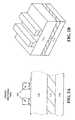
- FIGS. 5A and 5Billustrate thinning of the double fins of FIG. 4 consistent with the invention
- FIG. 6illustrates the formation of a bottom gate layer, gate insulation layer and channel layer for a planar FinFET consistent with another embodiment of the invention
- FIG. 7illustrates the formation of another gate insulation layer and a top gate layer on the channel layer of FIG. 6 consistent with another embodiment of the invention.
- FIGS. 8A and 8Billustrate the formation of a selected dielectric layer on a FinFET fin to induce strain within the FinFET channel consistent with yet another embodiment of the invention.
- an exemplary process for forming double fins for a double-gate FinFETis provided.
- the exemplary processmay employ thermal oxidation for thinning the double fins to create narrow fins, thereby improving device short-channel effects.
- FIG. 1illustrates a cross-section of a silicon on insulator (SOI) wafer 100 formed in accordance with an exemplary embodiment of the present invention.
- SOI wafer 100may include a buried oxide layer 110 formed on a substrate 115 .
- a fin layer 105may further be formed on buried oxide layer 110 .
- the thickness of fin layer 105may range, for example, from about 100 ⁇ to about 1000 ⁇ and the thickness of buried oxide layer 110 may range, for example, from about 1000 ⁇ to about 3000 ⁇ .
- Fin layer 105 and substrate 115may include, for example, silicon, though other semiconducting materials, such as germanium, may be used.
- a layer 120 of material, such as, for example, Si 3 N 4may be formed on fin layer 105 .
- Layer 120may be deposited on fin layer 105 and may range, for example, from about 50 ⁇ to about 500 ⁇ in thickness.
- caps 205may be defined in layer 120 .
- Caps 205may be defined, for example, using conventional etching processes and may have a width w 1 that ranges from about 50 ⁇ to about 500 ⁇ .
- Spacers 305may then be formed on the sides of caps 205 , as shown in FIG. 3 . Spacers 305 may be thermally grown, or deposited and etched, on the sides of caps 205 and may include, for example, an oxide material.
- the oxide materialmay include, for example, SiO or SiO 2 , though other oxide materials may be used.
- Two fins 405may be formed from fin layer 105 , as shown in FIG. 4 .
- Fins 405may be formed beneath spacers 305 and caps 205 using, for example, conventional etching processes. Fins 405 may include a width w 2 ranging from about 50 ⁇ to about 500 ⁇ . Thermal oxidation may then be performed and the oxide removed to thin down fins 405 to create thinned fins 505 , as shown in FIGS. 5A and 5B. The thickness t of thinned fins 505 may range from about 100 ⁇ to about 1000 ⁇ . Oxide spacers 305 may also be removed, as further shown in FIGS. 5A and 5B, during the oxide removal.
- the thinning of fins 505thereby, improves the short-channel effects in a double-gate FinFET that can result from the above-described process (with the addition of double gates that are not shown).
- the exemplary process described above for forming thinned fins for a double-gate FinFETadditionally may increase the device density, thus, reducing the device pitch.
- FIGS. 6-7illustrate an exemplary process for forming a planar double-gate FinFET with top/bottom gates using metal-induced crystallization.
- a layer 610 of oxidefor example, may be grown on a bulk wafer that includes a substrate 605 .
- Oxide layer 610may include, for example, SiO or SiO 2 , though other oxide materials may be used, and may range, for example, from about 100 ⁇ to about 500 ⁇ in thickness.
- a layer 615 of material for a bottom gatemay then be deposited on oxide layer 610 .
- Layer 615may include polysilicon or a metal material, such as, for example, TiN, W, or Mo, and may range from about 100 ⁇ to about 500 ⁇ in thickness.
- a gate insulation layer 620may then be deposited on layer 615 .
- Gate installation layer 620may include SiO, SiO 2 , SiN, SiON, HFO 2 , ZrO 2 , Al 2 O 3 , HfSiO(x) ZnS, MgF 2 , or other high-K dielectric materials. The thickness of gate insulation layer 620 may range, for example, from about 10 ⁇ to about 50 ⁇ .
- a channel layer 625may then be deposited on gate insulation layer 620 .
- Channel layer 625may include an amorphous silicon ( ⁇ -Si) material.
- Channel layer 625may additionally include a layer of deposited nickel (Ni). After deposition of the nickel layer, the channel layer 625 may be annealed to convert the amorphous silicon and Ni to crystalline silicon via metal induced crystallization.
- a second gate insulation layer 630may be deposited on channel layer 625 .
- Gate insulation layer 630may include SiO, SiO 2 , SiN, SiON, HFO 2 , ZrO 2 , Al 2 O 3 , HfSiO(x) ZnS, MgF 2 , or other high-K dielectric materials. The thickness of gate insulation layer 630 may range, for example, from about 10 ⁇ to about 50 ⁇ .
- a layer 635 of material for a top gatemay then be deposited on oxide layer gate insulation layer 630 .
- Layer 635may include polysilicon or a metal material, such as, for example, TiN, W, or Mo, and may range from about 100 ⁇ to about 500 ⁇ in thickness.
- the layers of material for the bottom gate and top gatemay then be etched (not shown) using conventional etching processes to provide appropriate definition for the gates.
- the resulting FinFETincludes a planar double-gate device with top and bottom gates that has a channel in between the top and bottom gates created using metal-induced crystallization.
- FIGS. 8A and 8Billustrate an exemplary FinFET gate dielectric, consistent with another embodiment of the invention, that improves FinFET carrier mobility.
- a fin 805may be formed on a substrate 810 , using any conventional technique, and a dielectric layer 815 may be thermally grown or deposited on the fin 805 .
- the dielectric material of dielectric layer 815may be chosen such that a desirable stress condition (i.e., due to tensile strain) may be created in fin 805 , which represents the channel region of the FinFET.
- the dielectric materialsuch as a high dielectric constant dielectric material, may be appropriately selected to create tensile strain in the material that comprises fin 805 .
- the induced tensile strainimproves carrier mobility of the channel region, thus, improving FinFET performance.
Landscapes
- Thin Film Transistor (AREA)
- Metal-Oxide And Bipolar Metal-Oxide Semiconductor Integrated Circuits (AREA)
- Insulated Gate Type Field-Effect Transistor (AREA)
Abstract
Description
Claims (14)
Priority Applications (8)
| Application Number | Priority Date | Filing Date | Title |
|---|---|---|---|
| US10/348,910US6762483B1 (en) | 2003-01-23 | 2003-01-23 | Narrow fin FinFET |
| CN2004800026970ACN1759488B (en) | 2003-01-23 | 2004-01-15 | narrow fin field effect transistor |
| KR1020057013667AKR101035421B1 (en) | 2003-01-23 | 2004-01-15 | Narrow Pins FINFET |
| PCT/US2004/000963WO2004068589A1 (en) | 2003-01-23 | 2004-01-15 | Narrow fin finfet |
| EP04702507AEP1588422A1 (en) | 2003-01-23 | 2004-01-15 | Narrow fin finfet |
| JP2006502826AJP2006516820A (en) | 2003-01-23 | 2004-01-15 | Method for forming fin FET with narrow fin structure |
| TW093101517ATW200418180A (en) | 2003-01-23 | 2004-01-20 | Narrow fin finFET |
| US10/830,006US6921963B2 (en) | 2003-01-23 | 2004-04-23 | Narrow fin FinFET |
Applications Claiming Priority (1)
| Application Number | Priority Date | Filing Date | Title |
|---|---|---|---|
| US10/348,910US6762483B1 (en) | 2003-01-23 | 2003-01-23 | Narrow fin FinFET |
Related Child Applications (1)
| Application Number | Title | Priority Date | Filing Date |
|---|---|---|---|
| US10/830,006ContinuationUS6921963B2 (en) | 2003-01-23 | 2004-04-23 | Narrow fin FinFET |
Publications (1)
| Publication Number | Publication Date |
|---|---|
| US6762483B1true US6762483B1 (en) | 2004-07-13 |
Family
ID=32681618
Family Applications (2)
| Application Number | Title | Priority Date | Filing Date |
|---|---|---|---|
| US10/348,910Expired - LifetimeUS6762483B1 (en) | 2003-01-23 | 2003-01-23 | Narrow fin FinFET |
| US10/830,006Expired - LifetimeUS6921963B2 (en) | 2003-01-23 | 2004-04-23 | Narrow fin FinFET |
Family Applications After (1)
| Application Number | Title | Priority Date | Filing Date |
|---|---|---|---|
| US10/830,006Expired - LifetimeUS6921963B2 (en) | 2003-01-23 | 2004-04-23 | Narrow fin FinFET |
Country Status (7)
| Country | Link |
|---|---|
| US (2) | US6762483B1 (en) |
| EP (1) | EP1588422A1 (en) |
| JP (1) | JP2006516820A (en) |
| KR (1) | KR101035421B1 (en) |
| CN (1) | CN1759488B (en) |
| TW (1) | TW200418180A (en) |
| WO (1) | WO2004068589A1 (en) |
Cited By (39)
| Publication number | Priority date | Publication date | Assignee | Title |
|---|---|---|---|---|
| US20040262687A1 (en)* | 2003-06-27 | 2004-12-30 | In-Soo Jung | Fin field effect transistors and fabrication methods thereof |
| US20050073022A1 (en)* | 2001-12-10 | 2005-04-07 | Karlsson Olov B. | Shallow trench isolation (STI) region with high-K liner and method of formation |
| US6894337B1 (en)* | 2004-02-02 | 2005-05-17 | Advanced Micro Devices, Inc. | System and method for forming stacked fin structure using metal-induced-crystallization |
| US20050104091A1 (en)* | 2003-11-04 | 2005-05-19 | Tabery Cyrus E. | Self aligned damascene gate |
| US20050287772A1 (en)* | 2004-06-07 | 2005-12-29 | Infineon Technologies Ag | Process for producing a web of a semiconductor material |
| US20060118892A1 (en)* | 2004-12-02 | 2006-06-08 | Taiwan Semiconductor Manufacturing Company, Ltd. | Methods and Structures to Produce a Strain-Inducing Layer in a Semiconductor Device |
| US7074623B2 (en) | 2002-06-07 | 2006-07-11 | Amberwave Systems Corporation | Methods of forming strained-semiconductor-on-insulator finFET device structures |
| US20070023756A1 (en)* | 2005-07-27 | 2007-02-01 | International Business Machines Corporation | Virtual body-contacted trigate |
| US20070131981A1 (en)* | 2003-10-15 | 2007-06-14 | Infineon Technologies Ag | Patterning method and field effect transistors |
| US20070290250A1 (en)* | 2004-03-18 | 2007-12-20 | Clark William F Jr | Multiple dielectric finfet structure and method |
| US7393733B2 (en) | 2004-12-01 | 2008-07-01 | Amberwave Systems Corporation | Methods of forming hybrid fin field-effect transistor structures |
| US20080203468A1 (en)* | 2007-02-28 | 2008-08-28 | Kangguo Cheng | FinFET with Reduced Gate to Fin Overlay Sensitivity |
| US7777250B2 (en) | 2006-03-24 | 2010-08-17 | Taiwan Semiconductor Manufacturing Company, Ltd. | Lattice-mismatched semiconductor structures and related methods for device fabrication |
| US7799592B2 (en) | 2006-09-27 | 2010-09-21 | Taiwan Semiconductor Manufacturing Company, Ltd. | Tri-gate field-effect transistors formed by aspect ratio trapping |
| US20100252862A1 (en)* | 2009-04-01 | 2010-10-07 | Chih-Hsin Ko | Source/Drain Engineering of Devices with High-Mobility Channels |
| US20100252816A1 (en)* | 2009-04-01 | 2010-10-07 | Taiwan Semiconductor Manufacturing Company, Ltd. | High-Mobility Multiple-Gate Transistor with Improved On-to-Off Current Ratio |
| US20100276668A1 (en)* | 2009-04-30 | 2010-11-04 | Chih-Hsin Ko | Reducing Source/Drain Resistance of III-V Based Transistors |
| US20100301390A1 (en)* | 2009-05-29 | 2010-12-02 | Chih-Hsin Ko | Gradient Ternary or Quaternary Multiple-Gate Transistor |
| US20100301392A1 (en)* | 2009-06-01 | 2010-12-02 | Chih-Hsin Ko | Source/Drain Re-Growth for Manufacturing III-V Based Transistors |
| US8216951B2 (en) | 2006-09-27 | 2012-07-10 | Taiwan Semiconductor Manufacturing Company, Ltd. | Quantum tunneling devices and circuits with lattice-mismatched semiconductor structures |
| US8237151B2 (en) | 2009-01-09 | 2012-08-07 | Taiwan Semiconductor Manufacturing Company, Ltd. | Diode-based devices and methods for making the same |
| US8253211B2 (en) | 2008-09-24 | 2012-08-28 | Taiwan Semiconductor Manufacturing Company, Ltd. | Semiconductor sensor structures with reduced dislocation defect densities |
| US8274097B2 (en) | 2008-07-01 | 2012-09-25 | Taiwan Semiconductor Manufacturing Company, Ltd. | Reduction of edge effects from aspect ratio trapping |
| US8304805B2 (en) | 2009-01-09 | 2012-11-06 | Taiwan Semiconductor Manufacturing Company, Ltd. | Semiconductor diodes fabricated by aspect ratio trapping with coalesced films |
| US8324660B2 (en) | 2005-05-17 | 2012-12-04 | Taiwan Semiconductor Manufacturing Company, Ltd. | Lattice-mismatched semiconductor structures with reduced dislocation defect densities and related methods for device fabrication |
| US8329541B2 (en) | 2007-06-15 | 2012-12-11 | Taiwan Semiconductor Manufacturing Company, Ltd. | InP-based transistor fabrication |
| US8344242B2 (en) | 2007-09-07 | 2013-01-01 | Taiwan Semiconductor Manufacturing Company, Ltd. | Multi-junction solar cells |
| US8384196B2 (en) | 2008-09-19 | 2013-02-26 | Taiwan Semiconductor Manufacturing Company, Ltd. | Formation of devices by epitaxial layer overgrowth |
| US8502263B2 (en) | 2006-10-19 | 2013-08-06 | Taiwan Semiconductor Manufacturing Company, Ltd. | Light-emitter-based devices with lattice-mismatched semiconductor structures |
| US8624103B2 (en) | 2007-04-09 | 2014-01-07 | Taiwan Semiconductor Manufacturing Company, Ltd. | Nitride-based multi-junction solar cell modules and methods for making the same |
| US8629446B2 (en) | 2009-04-02 | 2014-01-14 | Taiwan Semiconductor Manufacturing Company, Ltd. | Devices formed from a non-polar plane of a crystalline material and method of making the same |
| US8822248B2 (en) | 2008-06-03 | 2014-09-02 | Taiwan Semiconductor Manufacturing Company, Ltd. | Epitaxial growth of crystalline material |
| US8847279B2 (en) | 2006-09-07 | 2014-09-30 | Taiwan Semiconductor Manufacturing Company, Ltd. | Defect reduction using aspect ratio trapping |
| US8981427B2 (en) | 2008-07-15 | 2015-03-17 | Taiwan Semiconductor Manufacturing Company, Ltd. | Polishing of small composite semiconductor materials |
| US9508890B2 (en) | 2007-04-09 | 2016-11-29 | Taiwan Semiconductor Manufacturing Company, Ltd. | Photovoltaics on silicon |
| US9859381B2 (en) | 2005-05-17 | 2018-01-02 | Taiwan Semiconductor Manufacturing Company, Ltd. | Lattice-mismatched semiconductor structures with reduced dislocation defect densities and related methods for device fabrication |
| US9984872B2 (en) | 2008-09-19 | 2018-05-29 | Taiwan Semiconductor Manufacturing Company, Ltd. | Fabrication and structures of crystalline material |
| US10096524B1 (en) | 2017-10-18 | 2018-10-09 | International Business Machines Corporation | Semiconductor fin patterning techniques to achieve uniform fin profiles for fin field effect transistors |
| US11342442B2 (en) | 2012-07-17 | 2022-05-24 | Unm Rainforest Innovations | Semiconductor product comprising a heteroepitaxial layer grown on a seed area of a nanostructured pedestal |
Families Citing this family (141)
| Publication number | Priority date | Publication date | Assignee | Title |
|---|---|---|---|---|
| US6503783B1 (en)* | 2000-08-31 | 2003-01-07 | Micron Technology, Inc. | SOI CMOS device with reduced DIBL |
| US20060170053A1 (en)* | 2003-05-09 | 2006-08-03 | Yee-Chia Yeo | Accumulation mode multiple gate transistor |
| CN1799146A (en)* | 2003-05-30 | 2006-07-05 | 松下电器产业株式会社 | Semiconductor device and method for manufacturing same |
| US6909151B2 (en) | 2003-06-27 | 2005-06-21 | Intel Corporation | Nonplanar device with stress incorporation layer and method of fabrication |
| US7456476B2 (en) | 2003-06-27 | 2008-11-25 | Intel Corporation | Nonplanar semiconductor device with partially or fully wrapped around gate electrode and methods of fabrication |
| US6967175B1 (en) | 2003-12-04 | 2005-11-22 | Advanced Micro Devices, Inc. | Damascene gate semiconductor processing with local thinning of channel region |
| US7105390B2 (en) | 2003-12-30 | 2006-09-12 | Intel Corporation | Nonplanar transistors with metal gate electrodes |
| US7186599B2 (en) | 2004-01-12 | 2007-03-06 | Advanced Micro Devices, Inc. | Narrow-body damascene tri-gate FinFET |
| US7268058B2 (en)* | 2004-01-16 | 2007-09-11 | Intel Corporation | Tri-gate transistors and methods to fabricate same |
| KR100598099B1 (en)* | 2004-02-24 | 2006-07-07 | 삼성전자주식회사 | Vertical channel fin field effect transistor with damascene gate and method of manufacturing same |
| US7060539B2 (en)* | 2004-03-01 | 2006-06-13 | International Business Machines Corporation | Method of manufacture of FinFET devices with T-shaped fins and devices manufactured thereby |
| US6872640B1 (en)* | 2004-03-16 | 2005-03-29 | Micron Technology, Inc. | SOI CMOS device with reduced DIBL |
| US7154118B2 (en) | 2004-03-31 | 2006-12-26 | Intel Corporation | Bulk non-planar transistor having strained enhanced mobility and methods of fabrication |
| US7579280B2 (en) | 2004-06-01 | 2009-08-25 | Intel Corporation | Method of patterning a film |
| US7042009B2 (en)* | 2004-06-30 | 2006-05-09 | Intel Corporation | High mobility tri-gate devices and methods of fabrication |
| US7348284B2 (en) | 2004-08-10 | 2008-03-25 | Intel Corporation | Non-planar pMOS structure with a strained channel region and an integrated strained CMOS flow |
| US7009250B1 (en)* | 2004-08-20 | 2006-03-07 | Micron Technology, Inc. | FinFET device with reduced DIBL |
| KR100555573B1 (en)* | 2004-09-10 | 2006-03-03 | 삼성전자주식회사 | Semiconductor device having a junction region extended by SEB film and method for manufacturing same |
| US7422946B2 (en) | 2004-09-29 | 2008-09-09 | Intel Corporation | Independently accessed double-gate and tri-gate transistors in same process flow |
| US7332439B2 (en) | 2004-09-29 | 2008-02-19 | Intel Corporation | Metal gate transistors with epitaxial source and drain regions |
| US7361958B2 (en) | 2004-09-30 | 2008-04-22 | Intel Corporation | Nonplanar transistors with metal gate electrodes |
| US20060086977A1 (en) | 2004-10-25 | 2006-04-27 | Uday Shah | Nonplanar device with thinned lower body portion and method of fabrication |
| US7274053B2 (en)* | 2004-11-05 | 2007-09-25 | International Business Machines Corporation | Fin device with capacitor integrated under gate electrode |
| US7193279B2 (en)* | 2005-01-18 | 2007-03-20 | Intel Corporation | Non-planar MOS structure with a strained channel region |
| US7518196B2 (en) | 2005-02-23 | 2009-04-14 | Intel Corporation | Field effect transistor with narrow bandgap source and drain regions and method of fabrication |
| US20060202266A1 (en) | 2005-03-14 | 2006-09-14 | Marko Radosavljevic | Field effect transistor with metal source/drain regions |
| US7858481B2 (en) | 2005-06-15 | 2010-12-28 | Intel Corporation | Method for fabricating transistor with thinned channel |
| US7547637B2 (en) | 2005-06-21 | 2009-06-16 | Intel Corporation | Methods for patterning a semiconductor film |
| US7279375B2 (en) | 2005-06-30 | 2007-10-09 | Intel Corporation | Block contact architectures for nanoscale channel transistors |
| US7402875B2 (en) | 2005-08-17 | 2008-07-22 | Intel Corporation | Lateral undercut of metal gate in SOI device |
| US20070090416A1 (en) | 2005-09-28 | 2007-04-26 | Doyle Brian S | CMOS devices with a single work function gate electrode and method of fabrication |
| US7479421B2 (en) | 2005-09-28 | 2009-01-20 | Intel Corporation | Process for integrating planar and non-planar CMOS transistors on a bulk substrate and article made thereby |
| US7485503B2 (en) | 2005-11-30 | 2009-02-03 | Intel Corporation | Dielectric interface for group III-V semiconductor device |
| US7396711B2 (en)* | 2005-12-27 | 2008-07-08 | Intel Corporation | Method of fabricating a multi-cornered film |
| DE102006001680B3 (en) | 2006-01-12 | 2007-08-09 | Infineon Technologies Ag | Manufacturing method for a FinFET transistor arrangement and corresponding FinFET transistor arrangement |
| US7666741B2 (en) | 2006-01-17 | 2010-02-23 | International Business Machines Corporation | Corner clipping for field effect devices |
| US7449373B2 (en) | 2006-03-31 | 2008-11-11 | Intel Corporation | Method of ion implanting for tri-gate devices |
| US8143646B2 (en) | 2006-08-02 | 2012-03-27 | Intel Corporation | Stacking fault and twin blocking barrier for integrating III-V on Si |
| US7772048B2 (en)* | 2007-02-23 | 2010-08-10 | Freescale Semiconductor, Inc. | Forming semiconductor fins using a sacrificial fin |
| KR101443215B1 (en)* | 2007-06-13 | 2014-09-24 | 삼성전자주식회사 | Field-effect transistor and logic circuit using an amvipolar material |
| US7923337B2 (en) | 2007-06-20 | 2011-04-12 | International Business Machines Corporation | Fin field effect transistor devices with self-aligned source and drain regions |
| WO2009036273A2 (en)* | 2007-09-12 | 2009-03-19 | Arizona Board Of Regents For And On Behalf Of Arizona State University | Horizontally depleted metal semiconductor field effect transistor |
| US20090124097A1 (en)* | 2007-11-09 | 2009-05-14 | International Business Machines Corporation | Method of forming narrow fins in finfet devices with reduced spacing therebetween |
| US8003466B2 (en)* | 2008-04-08 | 2011-08-23 | Advanced Micro Devices, Inc. | Method of forming multiple fins for a semiconductor device |
| US8362566B2 (en) | 2008-06-23 | 2013-01-29 | Intel Corporation | Stress in trigate devices using complimentary gate fill materials |
| US20090321833A1 (en)* | 2008-06-25 | 2009-12-31 | International Business Machines Corporation | VERTICAL PROFILE FinFET GATE FORMED VIA PLATING UPON A THIN GATE DIELECTRIC |
| US7994020B2 (en)* | 2008-07-21 | 2011-08-09 | Advanced Micro Devices, Inc. | Method of forming finned semiconductor devices with trench isolation |
| US7871873B2 (en)* | 2009-03-27 | 2011-01-18 | Global Foundries Inc. | Method of forming fin structures using a sacrificial etch stop layer on bulk semiconductor material |
| US8258577B2 (en)* | 2009-06-04 | 2012-09-04 | International Business Machines Corporation | CMOS inverter device with fin structures |
| US7985639B2 (en)* | 2009-09-18 | 2011-07-26 | GlobalFoundries, Inc. | Method for fabricating a semiconductor device having a semiconductive resistor structure |
| US8101486B2 (en) | 2009-10-07 | 2012-01-24 | Globalfoundries Inc. | Methods for forming isolated fin structures on bulk semiconductor material |
| WO2011067821A1 (en)* | 2009-12-04 | 2011-06-09 | 株式会社 東芝 | Method for manufacturing semiconductor device |
| CN102263131B (en)* | 2010-05-25 | 2013-05-01 | 中国科学院微电子研究所 | Semiconductor device and forming method thereof |
| CN102315269B (en)* | 2010-07-01 | 2013-12-25 | 中国科学院微电子研究所 | Semiconductor device and forming method thereof |
| US8551829B2 (en) | 2010-11-10 | 2013-10-08 | United Microelectronics Corp. | Method for manufacturing multi-gate transistor device |
| US8361854B2 (en) | 2011-03-21 | 2013-01-29 | United Microelectronics Corp. | Fin field-effect transistor structure and manufacturing process thereof |
| US8597994B2 (en) | 2011-05-23 | 2013-12-03 | GlobalFoundries, Inc. | Semiconductor device and method of fabrication |
| US8614152B2 (en) | 2011-05-25 | 2013-12-24 | United Microelectronics Corp. | Gate structure and a method for forming the same |
| US8772860B2 (en) | 2011-05-26 | 2014-07-08 | United Microelectronics Corp. | FINFET transistor structure and method for making the same |
| US9184100B2 (en) | 2011-08-10 | 2015-11-10 | United Microelectronics Corp. | Semiconductor device having strained fin structure and method of making the same |
| US9105660B2 (en) | 2011-08-17 | 2015-08-11 | United Microelectronics Corp. | Fin-FET and method of forming the same |
| US8853013B2 (en) | 2011-08-19 | 2014-10-07 | United Microelectronics Corp. | Method for fabricating field effect transistor with fin structure |
| US8674433B2 (en) | 2011-08-24 | 2014-03-18 | United Microelectronics Corp. | Semiconductor process |
| US8691651B2 (en) | 2011-08-25 | 2014-04-08 | United Microelectronics Corp. | Method of forming non-planar FET |
| US8441072B2 (en) | 2011-09-02 | 2013-05-14 | United Microelectronics Corp. | Non-planar semiconductor structure and fabrication method thereof |
| US8497198B2 (en) | 2011-09-23 | 2013-07-30 | United Microelectronics Corp. | Semiconductor process |
| US8426277B2 (en) | 2011-09-23 | 2013-04-23 | United Microelectronics Corp. | Semiconductor process |
| US8722501B2 (en) | 2011-10-18 | 2014-05-13 | United Microelectronics Corp. | Method for manufacturing multi-gate transistor device |
| US8575708B2 (en) | 2011-10-26 | 2013-11-05 | United Microelectronics Corp. | Structure of field effect transistor with fin structure |
| US8871575B2 (en) | 2011-10-31 | 2014-10-28 | United Microelectronics Corp. | Method of fabricating field effect transistor with fin structure |
| US8278184B1 (en) | 2011-11-02 | 2012-10-02 | United Microelectronics Corp. | Fabrication method of a non-planar transistor |
| US8426283B1 (en) | 2011-11-10 | 2013-04-23 | United Microelectronics Corp. | Method of fabricating a double-gate transistor and a tri-gate transistor on a common substrate |
| US8440511B1 (en) | 2011-11-16 | 2013-05-14 | United Microelectronics Corp. | Method for manufacturing multi-gate transistor device |
| US8604548B2 (en) | 2011-11-23 | 2013-12-10 | United Microelectronics Corp. | Semiconductor device having ESD device |
| US8803247B2 (en) | 2011-12-15 | 2014-08-12 | United Microelectronics Corporation | Fin-type field effect transistor |
| US9087687B2 (en) | 2011-12-23 | 2015-07-21 | International Business Machines Corporation | Thin heterostructure channel device |
| US8609499B2 (en)* | 2012-01-09 | 2013-12-17 | Taiwan Semiconductor Manufacturing Company, Ltd. | FinFETs and the methods for forming the same |
| US8759184B2 (en) | 2012-01-09 | 2014-06-24 | Taiwan Semiconductor Manufacturing Company, Ltd. | FinFETs and the methods for forming the same |
| US8698199B2 (en) | 2012-01-11 | 2014-04-15 | United Microelectronics Corp. | FinFET structure |
| US9698229B2 (en) | 2012-01-17 | 2017-07-04 | United Microelectronics Corp. | Semiconductor structure and process thereof |
| US8946031B2 (en) | 2012-01-18 | 2015-02-03 | United Microelectronics Corp. | Method for fabricating MOS device |
| US8664060B2 (en) | 2012-02-07 | 2014-03-04 | United Microelectronics Corp. | Semiconductor structure and method of fabricating the same |
| US8822284B2 (en) | 2012-02-09 | 2014-09-02 | United Microelectronics Corp. | Method for fabricating FinFETs and semiconductor structure fabricated using the method |
| US9159809B2 (en) | 2012-02-29 | 2015-10-13 | United Microelectronics Corp. | Multi-gate transistor device |
| US9006107B2 (en) | 2012-03-11 | 2015-04-14 | United Microelectronics Corp. | Patterned structure of semiconductor device and fabricating method thereof |
| US9159626B2 (en) | 2012-03-13 | 2015-10-13 | United Microelectronics Corp. | FinFET and fabricating method thereof |
| US8946078B2 (en) | 2012-03-22 | 2015-02-03 | United Microelectronics Corp. | Method of forming trench in semiconductor substrate |
| US9559189B2 (en) | 2012-04-16 | 2017-01-31 | United Microelectronics Corp. | Non-planar FET |
| US9142649B2 (en) | 2012-04-23 | 2015-09-22 | United Microelectronics Corp. | Semiconductor structure with metal gate and method of fabricating the same |
| US8766319B2 (en) | 2012-04-26 | 2014-07-01 | United Microelectronics Corp. | Semiconductor device with ultra thin silicide layer |
| US8709910B2 (en) | 2012-04-30 | 2014-04-29 | United Microelectronics Corp. | Semiconductor process |
| US8691652B2 (en) | 2012-05-03 | 2014-04-08 | United Microelectronics Corp. | Semiconductor process |
| US8877623B2 (en) | 2012-05-14 | 2014-11-04 | United Microelectronics Corp. | Method of forming semiconductor device |
| US8470714B1 (en) | 2012-05-22 | 2013-06-25 | United Microelectronics Corp. | Method of forming fin structures in integrated circuits |
| US9012975B2 (en) | 2012-06-14 | 2015-04-21 | United Microelectronics Corp. | Field effect transistor and manufacturing method thereof |
| US8796695B2 (en) | 2012-06-22 | 2014-08-05 | United Microelectronics Corp. | Multi-gate field-effect transistor and process thereof |
| US8872280B2 (en) | 2012-07-31 | 2014-10-28 | United Microelectronics Corp. | Non-planar FET and manufacturing method thereof |
| US9318567B2 (en) | 2012-09-05 | 2016-04-19 | United Microelectronics Corp. | Fabrication method for semiconductor devices |
| US9159831B2 (en) | 2012-10-29 | 2015-10-13 | United Microelectronics Corp. | Multigate field effect transistor and process thereof |
| CN103839814B (en)* | 2012-11-21 | 2016-12-21 | 中芯国际集成电路制造(上海)有限公司 | The forming method of fin formula field effect transistor |
| US9536792B2 (en) | 2013-01-10 | 2017-01-03 | United Microelectronics Corp. | Complementary metal oxide semiconductor field effect transistor, metal oxide semiconductor field effect transistor and manufacturing method thereof |
| US9076870B2 (en) | 2013-02-21 | 2015-07-07 | United Microelectronics Corp. | Method for forming fin-shaped structure |
| US8841197B1 (en) | 2013-03-06 | 2014-09-23 | United Microelectronics Corp. | Method for forming fin-shaped structures |
| US9196500B2 (en) | 2013-04-09 | 2015-11-24 | United Microelectronics Corp. | Method for manufacturing semiconductor structures |
| US9711368B2 (en) | 2013-04-15 | 2017-07-18 | United Microelectronics Corp. | Sidewall image transfer process |
| US8853015B1 (en) | 2013-04-16 | 2014-10-07 | United Microelectronics Corp. | Method of forming a FinFET structure |
| US8709901B1 (en) | 2013-04-17 | 2014-04-29 | United Microelectronics Corp. | Method of forming an isolation structure |
| US9147747B2 (en) | 2013-05-02 | 2015-09-29 | United Microelectronics Corp. | Semiconductor structure with hard mask disposed on the gate structure |
| US9000483B2 (en) | 2013-05-16 | 2015-04-07 | United Microelectronics Corp. | Semiconductor device with fin structure and fabrication method thereof |
| US9263287B2 (en) | 2013-05-27 | 2016-02-16 | United Microelectronics Corp. | Method of forming fin-shaped structure |
| US8802521B1 (en) | 2013-06-04 | 2014-08-12 | United Microelectronics Corp. | Semiconductor fin-shaped structure and manufacturing process thereof |
| US9006804B2 (en) | 2013-06-06 | 2015-04-14 | United Microelectronics Corp. | Semiconductor device and fabrication method thereof |
| US9070710B2 (en) | 2013-06-07 | 2015-06-30 | United Microelectronics Corp. | Semiconductor process |
| US8993384B2 (en) | 2013-06-09 | 2015-03-31 | United Microelectronics Corp. | Semiconductor device and fabrication method thereof |
| US9263282B2 (en) | 2013-06-13 | 2016-02-16 | United Microelectronics Corporation | Method of fabricating semiconductor patterns |
| US9401429B2 (en) | 2013-06-13 | 2016-07-26 | United Microelectronics Corp. | Semiconductor structure and process thereof |
| US9123810B2 (en) | 2013-06-18 | 2015-09-01 | United Microelectronics Corp. | Semiconductor integrated device including FinFET device and protecting structure |
| US9048246B2 (en) | 2013-06-18 | 2015-06-02 | United Microelectronics Corp. | Die seal ring and method of forming the same |
| US9190291B2 (en) | 2013-07-03 | 2015-11-17 | United Microelectronics Corp. | Fin-shaped structure forming process |
| US9105685B2 (en) | 2013-07-12 | 2015-08-11 | United Microelectronics Corp. | Method of forming shallow trench isolation structure |
| US9093565B2 (en) | 2013-07-15 | 2015-07-28 | United Microelectronics Corp. | Fin diode structure |
| US9019672B2 (en) | 2013-07-17 | 2015-04-28 | United Microelectronics Corporation | Chip with electrostatic discharge protection function |
| US8981487B2 (en) | 2013-07-31 | 2015-03-17 | United Microelectronics Corp. | Fin-shaped field-effect transistor (FinFET) |
| US9006805B2 (en) | 2013-08-07 | 2015-04-14 | United Microelectronics Corp. | Semiconductor device |
| US9105582B2 (en) | 2013-08-15 | 2015-08-11 | United Microelectronics Corporation | Spatial semiconductor structure and method of fabricating the same |
| US9385048B2 (en) | 2013-09-05 | 2016-07-05 | United Microelectronics Corp. | Method of forming Fin-FET |
| US9373719B2 (en) | 2013-09-16 | 2016-06-21 | United Microelectronics Corp. | Semiconductor device |
| US9934981B2 (en)* | 2013-09-26 | 2018-04-03 | Varian Semiconductor Equipment Associates, Inc. | Techniques for processing substrates using directional reactive ion etching |
| US9018066B2 (en) | 2013-09-30 | 2015-04-28 | United Microelectronics Corp. | Method of fabricating semiconductor device structure |
| US9166024B2 (en) | 2013-09-30 | 2015-10-20 | United Microelectronics Corp. | FinFET structure with cavities and semiconductor compound portions extending laterally over sidewall spacers |
| US9306032B2 (en) | 2013-10-25 | 2016-04-05 | United Microelectronics Corp. | Method of forming self-aligned metal gate structure in a replacement gate process using tapered interlayer dielectric |
| US8980701B1 (en) | 2013-11-05 | 2015-03-17 | United Microelectronics Corp. | Method of forming semiconductor device |
| US9299843B2 (en) | 2013-11-13 | 2016-03-29 | United Microelectronics Corp. | Semiconductor structure and manufacturing method thereof |
| US8951884B1 (en) | 2013-11-14 | 2015-02-10 | United Microelectronics Corp. | Method for forming a FinFET structure |
| CN103681356A (en)* | 2013-12-27 | 2014-03-26 | 上海集成电路研发中心有限公司 | Method for manufacturing FinFET by using carbon nano tube as mask |
| US10854735B2 (en) | 2014-09-03 | 2020-12-01 | Taiwan Semiconductor Manufacturing Company Limited | Method of forming transistor |
| US9391074B1 (en) | 2015-04-21 | 2016-07-12 | International Business Machines Corporation | Structure for FinFET fins |
| US10008384B2 (en) | 2015-06-25 | 2018-06-26 | Varian Semiconductor Equipment Associates, Inc. | Techniques to engineer nanoscale patterned features using ions |
| US9935102B1 (en) | 2016-10-05 | 2018-04-03 | International Business Machines Corporation | Method and structure for improving vertical transistor |
| US11545575B2 (en) | 2020-07-02 | 2023-01-03 | Globalfoundries U.S. Inc. | IC structure with fin having subfin extents with different lateral dimensions |
| US11211453B1 (en) | 2020-07-23 | 2021-12-28 | Globalfoundries U.S. Inc. | FinFET with shorter fin height in drain region than source region and related method |
Citations (3)
| Publication number | Priority date | Publication date | Assignee | Title |
|---|---|---|---|---|
| US20030042531A1 (en)* | 2001-09-04 | 2003-03-06 | Lee Jong Ho | Flash memory element and manufacturing method thereof |
| US6583469B1 (en)* | 2002-01-28 | 2003-06-24 | International Business Machines Corporation | Self-aligned dog-bone structure for FinFET applications and methods to fabricate the same |
| US20040048424A1 (en)* | 2002-09-05 | 2004-03-11 | Taiwan Semiconductor Manufacturing Company | Method of forming an N channel and P channel FINFET device on the same semiconductor substrate |
Family Cites Families (17)
| Publication number | Priority date | Publication date | Assignee | Title |
|---|---|---|---|---|
| US5757038A (en)* | 1995-11-06 | 1998-05-26 | International Business Machines Corporation | Self-aligned dual gate MOSFET with an ultranarrow channel |
| US7163864B1 (en)* | 2000-10-18 | 2007-01-16 | International Business Machines Corporation | Method of fabricating semiconductor side wall fin |
| US6413802B1 (en)* | 2000-10-23 | 2002-07-02 | The Regents Of The University Of California | Finfet transistor structures having a double gate channel extending vertically from a substrate and methods of manufacture |
| US6472258B1 (en)* | 2000-11-13 | 2002-10-29 | International Business Machines Corporation | Double gate trench transistor |
| US6300182B1 (en)* | 2000-12-11 | 2001-10-09 | Advanced Micro Devices, Inc. | Field effect transistor having dual gates with asymmetrical doping for reduced threshold voltage |
| US6475869B1 (en)* | 2001-02-26 | 2002-11-05 | Advanced Micro Devices, Inc. | Method of forming a double gate transistor having an epitaxial silicon/germanium channel region |
| JP3543117B2 (en)* | 2001-03-13 | 2004-07-14 | 独立行政法人産業技術総合研究所 | Double gate field effect transistor |
| FR2822293B1 (en)* | 2001-03-13 | 2007-03-23 | Nat Inst Of Advanced Ind Scien | FIELD EFFECT TRANSISTOR AND DOUBLE GRID, INTEGRATED CIRCUIT COMPRISING THIS TRANSISTOR, AND METHOD OF MANUFACTURING THE SAME |
| JP2002289871A (en)* | 2001-03-28 | 2002-10-04 | Toshiba Corp | Semiconductor device and manufacturing method thereof |
| US6458662B1 (en)* | 2001-04-04 | 2002-10-01 | Advanced Micro Devices, Inc. | Method of fabricating a semiconductor device having an asymmetrical dual-gate silicon-germanium (SiGe) channel MOSFET and a device thereby formed |
| US6657259B2 (en) | 2001-12-04 | 2003-12-02 | International Business Machines Corporation | Multiple-plane FinFET CMOS |
| US6657252B2 (en) | 2002-03-19 | 2003-12-02 | International Business Machines Corporation | FinFET CMOS with NVRAM capability |
| US6750487B2 (en)* | 2002-04-11 | 2004-06-15 | International Business Machines Corporation | Dual double gate transistor |
| US6642090B1 (en) | 2002-06-03 | 2003-11-04 | International Business Machines Corporation | Fin FET devices from bulk semiconductor and method for forming |
| US6706571B1 (en) | 2002-10-22 | 2004-03-16 | Advanced Micro Devices, Inc. | Method for forming multiple structures in a semiconductor device |
| US6709982B1 (en) | 2002-11-26 | 2004-03-23 | Advanced Micro Devices, Inc. | Double spacer FinFET formation |
| US6645797B1 (en) | 2002-12-06 | 2003-11-11 | Advanced Micro Devices, Inc. | Method for forming fins in a FinFET device using sacrificial carbon layer |
- 2003
- 2003-01-23USUS10/348,910patent/US6762483B1/ennot_activeExpired - Lifetime
- 2004
- 2004-01-15WOPCT/US2004/000963patent/WO2004068589A1/enactiveSearch and Examination
- 2004-01-15KRKR1020057013667Apatent/KR101035421B1/ennot_activeExpired - Fee Related
- 2004-01-15EPEP04702507Apatent/EP1588422A1/ennot_activeCeased
- 2004-01-15JPJP2006502826Apatent/JP2006516820A/enactivePending
- 2004-01-15CNCN2004800026970Apatent/CN1759488B/ennot_activeExpired - Lifetime
- 2004-01-20TWTW093101517Apatent/TW200418180A/enunknown
- 2004-04-23USUS10/830,006patent/US6921963B2/ennot_activeExpired - Lifetime
Patent Citations (3)
| Publication number | Priority date | Publication date | Assignee | Title |
|---|---|---|---|---|
| US20030042531A1 (en)* | 2001-09-04 | 2003-03-06 | Lee Jong Ho | Flash memory element and manufacturing method thereof |
| US6583469B1 (en)* | 2002-01-28 | 2003-06-24 | International Business Machines Corporation | Self-aligned dog-bone structure for FinFET applications and methods to fabricate the same |
| US20040048424A1 (en)* | 2002-09-05 | 2004-03-11 | Taiwan Semiconductor Manufacturing Company | Method of forming an N channel and P channel FINFET device on the same semiconductor substrate |
Non-Patent Citations (8)
| Title |
|---|
| Co-pending U.S. Application Ser. No. 10/614,052 filed Jul. 8, 2003 entitled: "Narrow Fins By Oxidation In Double-Gate FinFET," 11 page specification, 7 sheets of drawings. |
| Copy of U.S. Ser. No. 10/699,887; filed Nov. 4, 2003; entitled: "Self Aligned Damascene Gate"; 35 pages. |
| Digh Hisamoto et al.: "FinFET-A Self-Aligned Double-Gate MOSFET Scalable to 20 nm," IEEE Transactions on Electron Devices, vol. 47, No. 12, Dec. 2000, pp. 2320-2325. |
| Digh Hisamoto et al.: "FinFET—A Self-Aligned Double-Gate MOSFET Scalable to 20 nm," IEEE Transactions on Electron Devices, vol. 47, No. 12, Dec. 2000, pp. 2320-2325. |
| Xuejue Huang et al.: "Sub 50-nm FinFET: PMOS," 0-7803-7050-3/01 IEEE, Sep. 1999 4 pages. |
| Xuejue Huang et al.: "Sub-50 nm P-Channel Fin FET," IEEE Transactions on Electron Devices, vol. 48, No. 5, May 2001, pp. 880-886. |
| Yang-Kyu Choi et al.: "Nanoscale CMOS Spacer FinFET for the Terabit Era," IEEE Electron Device Letters, vol. 23, No. 1, Jan. 2002, pp. 25-27. |
| Yang-Kyu Choi et al.: "Sub-20nm CMOS Fin FET Technologies," 0-7803-5410-9/99 IEEE, Mar. 2001, 4 pages. |
Cited By (110)
| Publication number | Priority date | Publication date | Assignee | Title |
|---|---|---|---|---|
| US6984569B2 (en)* | 2001-12-10 | 2006-01-10 | Advanced Micro Devices, Inc. | Shallow trench isolation (STI) region with high-K liner and method of formation |
| US20050073022A1 (en)* | 2001-12-10 | 2005-04-07 | Karlsson Olov B. | Shallow trench isolation (STI) region with high-K liner and method of formation |
| US7109516B2 (en) | 2002-06-07 | 2006-09-19 | Amberwave Systems Corporation | Strained-semiconductor-on-insulator finFET device structures |
| US7074623B2 (en) | 2002-06-07 | 2006-07-11 | Amberwave Systems Corporation | Methods of forming strained-semiconductor-on-insulator finFET device structures |
| US20070111439A1 (en)* | 2003-01-27 | 2007-05-17 | Samsung Electronics Co., Ltd. | Fin field effect transistors including epitaxial fins |
| US7176067B2 (en)* | 2003-06-27 | 2007-02-13 | Samsung Electronics Co., Ltd. | Methods of fabricating fin field effect transistors |
| US7394117B2 (en) | 2003-06-27 | 2008-07-01 | Samsung Electronics Co., Ltd. | Fin field effect transistors including epitaxial fins |
| US20040262687A1 (en)* | 2003-06-27 | 2004-12-30 | In-Soo Jung | Fin field effect transistors and fabrication methods thereof |
| US8278707B2 (en) | 2003-10-15 | 2012-10-02 | Infineon Technologies Ag | Field effect transistors having a double gate structure |
| US20100264472A1 (en)* | 2003-10-15 | 2010-10-21 | Infineon Technologies Ag | Patterning method, and field effect transistors |
| US20070131981A1 (en)* | 2003-10-15 | 2007-06-14 | Infineon Technologies Ag | Patterning method and field effect transistors |
| US7767100B2 (en)* | 2003-10-15 | 2010-08-03 | Infineon Technologies Ag | Patterning method and field effect transistors |
| US20050104091A1 (en)* | 2003-11-04 | 2005-05-19 | Tabery Cyrus E. | Self aligned damascene gate |
| US7029958B2 (en)* | 2003-11-04 | 2006-04-18 | Advanced Micro Devices, Inc. | Self aligned damascene gate |
| US6894337B1 (en)* | 2004-02-02 | 2005-05-17 | Advanced Micro Devices, Inc. | System and method for forming stacked fin structure using metal-induced-crystallization |
| US20070290250A1 (en)* | 2004-03-18 | 2007-12-20 | Clark William F Jr | Multiple dielectric finfet structure and method |
| US20050287772A1 (en)* | 2004-06-07 | 2005-12-29 | Infineon Technologies Ag | Process for producing a web of a semiconductor material |
| US8183627B2 (en) | 2004-12-01 | 2012-05-22 | Taiwan Semiconductor Manufacturing Company, Ltd. | Hybrid fin field-effect transistor structures and related methods |
| US7393733B2 (en) | 2004-12-01 | 2008-07-01 | Amberwave Systems Corporation | Methods of forming hybrid fin field-effect transistor structures |
| US20060118892A1 (en)* | 2004-12-02 | 2006-06-08 | Taiwan Semiconductor Manufacturing Company, Ltd. | Methods and Structures to Produce a Strain-Inducing Layer in a Semiconductor Device |
| US9859381B2 (en) | 2005-05-17 | 2018-01-02 | Taiwan Semiconductor Manufacturing Company, Ltd. | Lattice-mismatched semiconductor structures with reduced dislocation defect densities and related methods for device fabrication |
| US8324660B2 (en) | 2005-05-17 | 2012-12-04 | Taiwan Semiconductor Manufacturing Company, Ltd. | Lattice-mismatched semiconductor structures with reduced dislocation defect densities and related methods for device fabrication |
| US8629477B2 (en) | 2005-05-17 | 2014-01-14 | Taiwan Semiconductor Manufacturing Company, Ltd. | Lattice-mismatched semiconductor structures with reduced dislocation defect densities and related methods for device fabrication |
| US9431243B2 (en) | 2005-05-17 | 2016-08-30 | Taiwan Semiconductor Manufacturing Company, Ltd. | Lattice-mismatched semiconductor structures with reduced dislocation defect densities and related methods for device fabrication |
| US11251272B2 (en) | 2005-05-17 | 2022-02-15 | Taiwan Semiconductor Manufacturing Company, Ltd. | Lattice-mismatched semiconductor structures with reduced dislocation defect densities and related methods for device fabrication |
| US8796734B2 (en) | 2005-05-17 | 2014-08-05 | Taiwan Semiconductor Manufacturing Company, Ltd. | Lattice-mismatched semiconductor structures with reduced dislocation defect densities and related methods for device fabrication |
| US8519436B2 (en) | 2005-05-17 | 2013-08-27 | Taiwan Semiconductor Manufacturing Company, Ltd. | Lattice-mismatched semiconductor structures with reduced dislocation defect densities and related methods for device fabrication |
| US9219112B2 (en) | 2005-05-17 | 2015-12-22 | Taiwan Semiconductor Manufacturing Company, Ltd. | Lattice-mismatched semiconductor structures with reduced dislocation defect densities and related methods for device fabrication |
| US10522629B2 (en) | 2005-05-17 | 2019-12-31 | Taiwan Semiconductor Manufacturing Company, Ltd. | Lattice-mismatched semiconductor structures with reduced dislocation defect densities and related methods for device fabrication |
| US8987028B2 (en) | 2005-05-17 | 2015-03-24 | Taiwan Semiconductor Manufacturing Company, Ltd. | Lattice-mismatched semiconductor structures with reduced dislocation defect densities and related methods for device fabrication |
| US20070023756A1 (en)* | 2005-07-27 | 2007-02-01 | International Business Machines Corporation | Virtual body-contacted trigate |
| US7700446B2 (en) | 2005-07-27 | 2010-04-20 | International Business Machines Corporation | Virtual body-contacted trigate |
| US20080176363A1 (en)* | 2005-07-27 | 2008-07-24 | Anderson Brent A | Virtual body-contacted trigate |
| US7288802B2 (en) | 2005-07-27 | 2007-10-30 | International Business Machines Corporation | Virtual body-contacted trigate |
| US8878243B2 (en) | 2006-03-24 | 2014-11-04 | Taiwan Semiconductor Manufacturing Company, Ltd. | Lattice-mismatched semiconductor structures and related methods for device fabrication |
| US7777250B2 (en) | 2006-03-24 | 2010-08-17 | Taiwan Semiconductor Manufacturing Company, Ltd. | Lattice-mismatched semiconductor structures and related methods for device fabrication |
| US10074536B2 (en) | 2006-03-24 | 2018-09-11 | Taiwan Semiconductor Manufacturing Company, Ltd. | Lattice-mismatched semiconductor structures and related methods for device fabrication |
| US9818819B2 (en) | 2006-09-07 | 2017-11-14 | Taiwan Semiconductor Manufacturing Company, Ltd. | Defect reduction using aspect ratio trapping |
| US8847279B2 (en) | 2006-09-07 | 2014-09-30 | Taiwan Semiconductor Manufacturing Company, Ltd. | Defect reduction using aspect ratio trapping |
| US9318325B2 (en) | 2006-09-07 | 2016-04-19 | Taiwan Semiconductor Manufacturing Company, Ltd. | Defect reduction using aspect ratio trapping |
| US8860160B2 (en) | 2006-09-27 | 2014-10-14 | Taiwan Semiconductor Manufacturing Company, Ltd. | Quantum tunneling devices and circuits with lattice-mismatched semiconductor structures |
| US9559712B2 (en) | 2006-09-27 | 2017-01-31 | Taiwan Semiconductor Manufacturing Company, Ltd. | Quantum tunneling devices and circuits with lattice-mismatched semiconductor structures |
| US9105522B2 (en) | 2006-09-27 | 2015-08-11 | Taiwan Semiconductor Manufacturing Company, Ltd. | Quantum tunneling devices and circuits with lattice-mismatched semiconductor structures |
| US8216951B2 (en) | 2006-09-27 | 2012-07-10 | Taiwan Semiconductor Manufacturing Company, Ltd. | Quantum tunneling devices and circuits with lattice-mismatched semiconductor structures |
| US7799592B2 (en) | 2006-09-27 | 2010-09-21 | Taiwan Semiconductor Manufacturing Company, Ltd. | Tri-gate field-effect transistors formed by aspect ratio trapping |
| US8629047B2 (en) | 2006-09-27 | 2014-01-14 | Taiwan Semiconductor Manufacturing Company, Ltd. | Quantum tunneling devices and circuits with lattice-mismatched semiconductor structures |
| US8502263B2 (en) | 2006-10-19 | 2013-08-06 | Taiwan Semiconductor Manufacturing Company, Ltd. | Light-emitter-based devices with lattice-mismatched semiconductor structures |
| US10468551B2 (en) | 2006-10-19 | 2019-11-05 | Taiwan Semiconductor Manufacturing Company, Ltd. | Light-emitter-based devices with lattice-mismatched semiconductor structures |
| US8518767B2 (en) | 2007-02-28 | 2013-08-27 | International Business Machines Corporation | FinFET with reduced gate to fin overlay sensitivity |
| US8536632B2 (en) | 2007-02-28 | 2013-09-17 | International Business Machines Corporation | FinFET with reduced gate to fin overlay sensitivity |
| US20080203468A1 (en)* | 2007-02-28 | 2008-08-28 | Kangguo Cheng | FinFET with Reduced Gate to Fin Overlay Sensitivity |
| US9508890B2 (en) | 2007-04-09 | 2016-11-29 | Taiwan Semiconductor Manufacturing Company, Ltd. | Photovoltaics on silicon |
| US8624103B2 (en) | 2007-04-09 | 2014-01-07 | Taiwan Semiconductor Manufacturing Company, Ltd. | Nitride-based multi-junction solar cell modules and methods for making the same |
| US9040331B2 (en) | 2007-04-09 | 2015-05-26 | Taiwan Semiconductor Manufacturing Company, Ltd. | Diode-based devices and methods for making the same |
| US9543472B2 (en) | 2007-04-09 | 2017-01-10 | Taiwan Semiconductor Manufacturing Company, Ltd. | Diode-based devices and methods for making the same |
| US9853118B2 (en) | 2007-04-09 | 2017-12-26 | Taiwan Semiconductor Manufacturing Company, Ltd. | Diode-based devices and methods for making the same |
| US9231073B2 (en) | 2007-04-09 | 2016-01-05 | Taiwan Semiconductor Manufacturing Company, Ltd. | Diode-based devices and methods for making the same |
| US9853176B2 (en) | 2007-04-09 | 2017-12-26 | Taiwan Semiconductor Manufacturing Company, Ltd. | Nitride-based multi-junction solar cell modules and methods for making the same |
| US10680126B2 (en) | 2007-04-09 | 2020-06-09 | Taiwan Semiconductor Manufacturing Company, Ltd. | Photovoltaics on silicon |
| US8329541B2 (en) | 2007-06-15 | 2012-12-11 | Taiwan Semiconductor Manufacturing Company, Ltd. | InP-based transistor fabrication |
| US9780190B2 (en) | 2007-06-15 | 2017-10-03 | Taiwan Semiconductor Manufacturing Company, Ltd. | InP-based transistor fabrication |
| US8344242B2 (en) | 2007-09-07 | 2013-01-01 | Taiwan Semiconductor Manufacturing Company, Ltd. | Multi-junction solar cells |
| US10002981B2 (en) | 2007-09-07 | 2018-06-19 | Taiwan Semiconductor Manufacturing Company, Ltd. | Multi-junction solar cells |
| US9365949B2 (en) | 2008-06-03 | 2016-06-14 | Taiwan Semiconductor Manufacturing Company, Ltd. | Epitaxial growth of crystalline material |
| US10961639B2 (en) | 2008-06-03 | 2021-03-30 | Taiwan Semiconductor Manufacturing Company, Ltd. | Epitaxial growth of crystalline material |
| US8822248B2 (en) | 2008-06-03 | 2014-09-02 | Taiwan Semiconductor Manufacturing Company, Ltd. | Epitaxial growth of crystalline material |
| US8629045B2 (en) | 2008-07-01 | 2014-01-14 | Taiwan Semiconductor Manufacturing Company, Ltd. | Reduction of edge effects from aspect ratio trapping |
| US9356103B2 (en) | 2008-07-01 | 2016-05-31 | Taiwan Semiconductor Manufacturing Company, Ltd. | Reduction of edge effects from aspect ratio trapping |
| US9640395B2 (en) | 2008-07-01 | 2017-05-02 | Taiwan Semiconductor Manufacturing Company, Ltd. | Reduction of edge effects from aspect ratio trapping |
| US8994070B2 (en) | 2008-07-01 | 2015-03-31 | Taiwan Semiconductor Manufacturing Company, Ltd. | Reduction of edge effects from aspect ratio trapping |
| US8274097B2 (en) | 2008-07-01 | 2012-09-25 | Taiwan Semiconductor Manufacturing Company, Ltd. | Reduction of edge effects from aspect ratio trapping |
| US8981427B2 (en) | 2008-07-15 | 2015-03-17 | Taiwan Semiconductor Manufacturing Company, Ltd. | Polishing of small composite semiconductor materials |
| US9287128B2 (en) | 2008-07-15 | 2016-03-15 | Taiwan Semiconductor Manufacturing Company, Ltd. | Polishing of small composite semiconductor materials |
| US9607846B2 (en) | 2008-07-15 | 2017-03-28 | Taiwan Semiconductor Manufacturing Company, Ltd. | Polishing of small composite semiconductor materials |
| US9934967B2 (en) | 2008-09-19 | 2018-04-03 | Taiwan Semiconductor Manufacturing Co., Ltd. | Formation of devices by epitaxial layer overgrowth |
| US8384196B2 (en) | 2008-09-19 | 2013-02-26 | Taiwan Semiconductor Manufacturing Company, Ltd. | Formation of devices by epitaxial layer overgrowth |
| US9984872B2 (en) | 2008-09-19 | 2018-05-29 | Taiwan Semiconductor Manufacturing Company, Ltd. | Fabrication and structures of crystalline material |
| US8809106B2 (en) | 2008-09-24 | 2014-08-19 | Taiwan Semiconductor Manufacturing Company, Ltd. | Method for semiconductor sensor structures with reduced dislocation defect densities |
| US8253211B2 (en) | 2008-09-24 | 2012-08-28 | Taiwan Semiconductor Manufacturing Company, Ltd. | Semiconductor sensor structures with reduced dislocation defect densities |
| US9455299B2 (en) | 2008-09-24 | 2016-09-27 | Taiwan Semiconductor Manufacturing Company, Ltd. | Methods for semiconductor sensor structures with reduced dislocation defect densities |
| US9105549B2 (en) | 2008-09-24 | 2015-08-11 | Taiwan Semiconductor Manufacturing Company, Ltd. | Semiconductor sensor structures with reduced dislocation defect densities |
| US8304805B2 (en) | 2009-01-09 | 2012-11-06 | Taiwan Semiconductor Manufacturing Company, Ltd. | Semiconductor diodes fabricated by aspect ratio trapping with coalesced films |
| US8237151B2 (en) | 2009-01-09 | 2012-08-07 | Taiwan Semiconductor Manufacturing Company, Ltd. | Diode-based devices and methods for making the same |
| US9590068B2 (en) | 2009-04-01 | 2017-03-07 | Taiwan Semiconductor Manufacturing Company, Ltd. | High-mobility multiple-gate transistor with improved on-to-off current ratio |
| US20100252816A1 (en)* | 2009-04-01 | 2010-10-07 | Taiwan Semiconductor Manufacturing Company, Ltd. | High-Mobility Multiple-Gate Transistor with Improved On-to-Off Current Ratio |
| US20100252862A1 (en)* | 2009-04-01 | 2010-10-07 | Chih-Hsin Ko | Source/Drain Engineering of Devices with High-Mobility Channels |
| US10109748B2 (en) | 2009-04-01 | 2018-10-23 | Taiwan Semiconductor Manufacturing Company, Ltd. | High-mobility multiple-gate transistor with improved on-to-off current ratio |
| US8674341B2 (en) | 2009-04-01 | 2014-03-18 | Taiwan Semiconductor Manufacturing Company, Ltd. | High-mobility multiple-gate transistor with improved on-to-off current ratio |
| US8927371B2 (en) | 2009-04-01 | 2015-01-06 | Taiwan Semiconductor Manufacturing Company, Ltd. | High-mobility multiple-gate transistor with improved on-to-off current ratio |
| US8816391B2 (en) | 2009-04-01 | 2014-08-26 | Taiwan Semiconductor Manufacturing Company, Ltd. | Source/drain engineering of devices with high-mobility channels |
| US9576951B2 (en) | 2009-04-02 | 2017-02-21 | Taiwan Semiconductor Manufacturing Company, Ltd. | Devices formed from a non-polar plane of a crystalline material and method of making the same |
| US8629446B2 (en) | 2009-04-02 | 2014-01-14 | Taiwan Semiconductor Manufacturing Company, Ltd. | Devices formed from a non-polar plane of a crystalline material and method of making the same |
| US9299562B2 (en) | 2009-04-02 | 2016-03-29 | Taiwan Semiconductor Manufacturing Company, Ltd. | Devices formed from a non-polar plane of a crystalline material and method of making the same |
| US8455860B2 (en) | 2009-04-30 | 2013-06-04 | Taiwan Semiconductor Manufacturing Company, Ltd. | Reducing source/drain resistance of III-V based transistors |
| US8674408B2 (en) | 2009-04-30 | 2014-03-18 | Taiwan Semiconductor Manufacturing Company, Ltd. | Reducing source/drain resistance of III-V based transistors |
| US20100276668A1 (en)* | 2009-04-30 | 2010-11-04 | Chih-Hsin Ko | Reducing Source/Drain Resistance of III-V Based Transistors |
| US10269970B2 (en) | 2009-05-29 | 2019-04-23 | Taiwan Semiconductor Manufacturing Company, Ltd. | Gradient ternary or quaternary multiple-gate transistor |
| US9768305B2 (en) | 2009-05-29 | 2017-09-19 | Taiwan Semiconductor Manufacturing Company, Ltd. | Gradient ternary or quaternary multiple-gate transistor |
| US20100301390A1 (en)* | 2009-05-29 | 2010-12-02 | Chih-Hsin Ko | Gradient Ternary or Quaternary Multiple-Gate Transistor |
| US9006788B2 (en) | 2009-06-01 | 2015-04-14 | Taiwan Semiconductor Manufacturing Company, Ltd. | Source/drain re-growth for manufacturing III-V based transistors |
| US8617976B2 (en) | 2009-06-01 | 2013-12-31 | Taiwan Semiconductor Manufacturing Company, Ltd. | Source/drain re-growth for manufacturing III-V based transistors |
| US20100301392A1 (en)* | 2009-06-01 | 2010-12-02 | Chih-Hsin Ko | Source/Drain Re-Growth for Manufacturing III-V Based Transistors |
| US11342438B1 (en) | 2012-07-17 | 2022-05-24 | Unm Rainforest Innovations | Device with heteroepitaxial structure made using a growth mask |
| US11342442B2 (en) | 2012-07-17 | 2022-05-24 | Unm Rainforest Innovations | Semiconductor product comprising a heteroepitaxial layer grown on a seed area of a nanostructured pedestal |
| US11342441B2 (en) | 2012-07-17 | 2022-05-24 | Unm Rainforest Innovations | Method of forming a seed area and growing a heteroepitaxial layer on the seed area |
| US11349011B2 (en) | 2012-07-17 | 2022-05-31 | Unm Rainforest Innovations | Method of making heteroepitaxial structures and device formed by the method |
| US11374106B2 (en) | 2012-07-17 | 2022-06-28 | Unm Rainforest Innovations | Method of making heteroepitaxial structures and device formed by the method |
| US11456370B2 (en) | 2012-07-17 | 2022-09-27 | Unm Rainforest Innovations | Semiconductor product comprising a heteroepitaxial layer grown on a seed area of a nanostructured pedestal |
| US10325817B2 (en) | 2017-10-18 | 2019-06-18 | International Business Machines Corporation | Semiconductor fin patterning techniques to achieve uniform fin profiles for fin field effect transistors |
| US10096524B1 (en) | 2017-10-18 | 2018-10-09 | International Business Machines Corporation | Semiconductor fin patterning techniques to achieve uniform fin profiles for fin field effect transistors |
Also Published As
| Publication number | Publication date |
|---|---|
| JP2006516820A (en) | 2006-07-06 |
| KR20050096156A (en) | 2005-10-05 |
| US20040197975A1 (en) | 2004-10-07 |
| KR101035421B1 (en) | 2011-05-20 |
| EP1588422A1 (en) | 2005-10-26 |
| WO2004068589A1 (en) | 2004-08-12 |
| US6921963B2 (en) | 2005-07-26 |
| CN1759488A (en) | 2006-04-12 |
| TW200418180A (en) | 2004-09-16 |
| CN1759488B (en) | 2010-08-18 |
Similar Documents
| Publication | Publication Date | Title |
|---|---|---|
| US6762483B1 (en) | Narrow fin FinFET | |
| US6812119B1 (en) | Narrow fins by oxidation in double-gate finfet | |
| EP1593161B1 (en) | Strained channel finfet | |
| US7250645B1 (en) | Reversed T-shaped FinFET | |
| US6686231B1 (en) | Damascene gate process with sacrificial oxide in semiconductor devices | |
| US7084018B1 (en) | Sacrificial oxide for minimizing box undercut in damascene FinFET | |
| US6855990B2 (en) | Strained-channel multiple-gate transistor | |
| US6611029B1 (en) | Double gate semiconductor device having separate gates | |
| US6833588B2 (en) | Semiconductor device having a U-shaped gate structure | |
| US6787439B2 (en) | Method using planarizing gate material to improve gate critical dimension in semiconductor devices | |
| US7186599B2 (en) | Narrow-body damascene tri-gate FinFET | |
| US6762448B1 (en) | FinFET device with multiple fin structures | |
| US6645797B1 (en) | Method for forming fins in a FinFET device using sacrificial carbon layer | |
| US8008136B2 (en) | Fully silicided gate structure for FinFET devices | |
| CN105023840B (en) | Strained semiconductor device with recessed channel and method of forming the same | |
| US6998301B1 (en) | Method for forming a tri-gate MOSFET | |
| US20100308409A1 (en) | Finfet structures with fins having stress-inducing caps and methods for fabricating the same | |
| US6855989B1 (en) | Damascene finfet gate with selective metal interdiffusion | |
| US6876042B1 (en) | Additional gate control for a double-gate MOSFET | |
| US9911601B2 (en) | Epitaxial silicon germanium fin formation using sacrificial silicon fin templates | |
| US6967175B1 (en) | Damascene gate semiconductor processing with local thinning of channel region | |
| US7498225B1 (en) | Systems and methods for forming multiple fin structures using metal-induced-crystallization | |
| US12021117B2 (en) | Semiconductor structure and method of forming the same |
Legal Events
| Date | Code | Title | Description |
|---|---|---|---|
| AS | Assignment | Owner name:ADVANCE MICRO DEVICES, INC., CALIFORNIA Free format text:ASSIGNMENT OF ASSIGNORS INTEREST;ASSIGNORS:KRIVOKAPIC, ZORAN;AN, JUDY XILIN;DAKSHINA-MURTHY, SRIKANTESWARA;AND OTHERS;REEL/FRAME:014140/0431 Effective date:20030110 | |
| FEPP | Fee payment procedure | Free format text:PAYOR NUMBER ASSIGNED (ORIGINAL EVENT CODE: ASPN); ENTITY STATUS OF PATENT OWNER: LARGE ENTITY | |
| STCF | Information on status: patent grant | Free format text:PATENTED CASE | |
| FPAY | Fee payment | Year of fee payment:4 | |
| CC | Certificate of correction | ||
| AS | Assignment | Owner name:GLOBALFOUNDRIES INC., CAYMAN ISLANDS Free format text:AFFIRMATION OF PATENT ASSIGNMENT;ASSIGNOR:ADVANCED MICRO DEVICES, INC.;REEL/FRAME:023119/0083 Effective date:20090630 | |
| FPAY | Fee payment | Year of fee payment:8 | |
| FPAY | Fee payment | Year of fee payment:12 | |
| AS | Assignment | Owner name:WILMINGTON TRUST, NATIONAL ASSOCIATION, DELAWARE Free format text:SECURITY AGREEMENT;ASSIGNOR:GLOBALFOUNDRIES INC.;REEL/FRAME:049490/0001 Effective date:20181127 | |
| AS | Assignment | Owner name:GLOBALFOUNDRIES U.S. INC., CALIFORNIA Free format text:ASSIGNMENT OF ASSIGNORS INTEREST;ASSIGNOR:GLOBALFOUNDRIES INC.;REEL/FRAME:054633/0001 Effective date:20201022 | |
| AS | Assignment | Owner name:GLOBALFOUNDRIES INC., CAYMAN ISLANDS Free format text:RELEASE BY SECURED PARTY;ASSIGNOR:WILMINGTON TRUST, NATIONAL ASSOCIATION;REEL/FRAME:054636/0001 Effective date:20201117 | |
| AS | Assignment | Owner name:GLOBALFOUNDRIES U.S. INC., NEW YORK Free format text:RELEASE BY SECURED PARTY;ASSIGNOR:WILMINGTON TRUST, NATIONAL ASSOCIATION;REEL/FRAME:056987/0001 Effective date:20201117 |