US6762450B2 - Method of forming a capacitor and a capacitor construction - Google Patents
Method of forming a capacitor and a capacitor constructionDownload PDFInfo
- Publication number
- US6762450B2 US6762450B2US09/876,102US87610201AUS6762450B2US 6762450 B2US6762450 B2US 6762450B2US 87610201 AUS87610201 AUS 87610201AUS 6762450 B2US6762450 B2US 6762450B2
- Authority
- US
- United States
- Prior art keywords
- conductive
- layer
- opening
- node
- pair
- Prior art date
- Legal status (The legal status is an assumption and is not a legal conclusion. Google has not performed a legal analysis and makes no representation as to the accuracy of the status listed.)
- Expired - Fee Related, expires
Links
Images


Classifications
- H—ELECTRICITY
- H10—SEMICONDUCTOR DEVICES; ELECTRIC SOLID-STATE DEVICES NOT OTHERWISE PROVIDED FOR
- H10D—INORGANIC ELECTRIC SEMICONDUCTOR DEVICES
- H10D1/00—Resistors, capacitors or inductors
- H10D1/01—Manufacture or treatment
- H10D1/041—Manufacture or treatment of capacitors having no potential barriers
- H10D1/042—Manufacture or treatment of capacitors having no potential barriers using deposition processes to form electrode extensions
- H—ELECTRICITY
- H10—SEMICONDUCTOR DEVICES; ELECTRIC SOLID-STATE DEVICES NOT OTHERWISE PROVIDED FOR
- H10D—INORGANIC ELECTRIC SEMICONDUCTOR DEVICES
- H10D1/00—Resistors, capacitors or inductors
- H10D1/60—Capacitors
- H10D1/68—Capacitors having no potential barriers
- H10D1/692—Electrodes
- H10D1/711—Electrodes having non-planar surfaces, e.g. formed by texturisation
- H10D1/714—Electrodes having non-planar surfaces, e.g. formed by texturisation having horizontal extensions
- H—ELECTRICITY
- H10—SEMICONDUCTOR DEVICES; ELECTRIC SOLID-STATE DEVICES NOT OTHERWISE PROVIDED FOR
- H10B—ELECTRONIC MEMORY DEVICES
- H10B12/00—Dynamic random access memory [DRAM] devices
- H10B12/01—Manufacture or treatment
- H10B12/02—Manufacture or treatment for one transistor one-capacitor [1T-1C] memory cells
- H10B12/03—Making the capacitor or connections thereto
- H10B12/033—Making the capacitor or connections thereto the capacitor extending over the transistor
- H10B12/0335—Making a connection between the transistor and the capacitor, e.g. plug
Definitions
- This inventionrelates generally to capacitor formation in semiconductor wafer processing, and to resultant capacitor constructions.
- cell structure techniquesinclude three-dimensional cell capacitors, such as trenched or stacked capacitors.
- This inventionconcerns stacked capacitor cell constructions, including what are commonly known as crown or cylindrical container stacked capacitors.
- FIG. 1is a diagrammatic sectional view of a semiconductor wafer fragment at one processing step in accordance with the invention.
- FIG. 2is a view of the FIG. 1 wafer fragment at a processing step subsequent to that shown by FIG. 1 .
- FIG. 3is a view of the FIG. 1 wafer fragment at a processing step subsequent to that shown by FIG. 2 .
- FIG. 4is a view of the FIG. 1 wafer fragment at a processing step subsequent to that shown by FIG. 3 .
- FIG. 5is a view of the FIG. 1 wafer fragment at a processing step subsequent to that shown by FIG. 4 .
- FIG. 6is a view of the FIG. 1 wafer fragment at a processing step subsequent to that shown by FIG. 5 .
- FIG. 7is a view of the FIG. 1 wafer fragment at a processing step subsequent to that shown by FIG. 6 .
- FIG. 8is a view of the FIG. 1 wafer fragment at a processing step subsequent to that shown by FIG. 7 .
- FIG. 9is a view of the FIG. 1 wafer fragment at a processing step subsequent to that shown by FIG. 8 .
- FIG. 10is a view of the FIG. 1 wafer fragment at a processing step subsequent to that shown by FIG. 9 .
- FIG. 11is a view of the FIG. 1 wafer fragment at a processing step subsequent to that shown by FIG. 10 .
- FIG. 12is a view of the FIG. 1 wafer fragment at a processing step subsequent to that shown by FIG. 11 .
- FIG. 13is a diagrammatic sectional view of an alternate embodiment semiconductor wafer fragment at a processing step in accordance with the invention.
- FIG. 14is a view of the FIG. 13 wafer fragment at a processing step subsequent to that shown by FIG. 13 .
- FIG. 15is a view of the FIG. 13 wafer fragment at a processing step subsequent to that shown by FIG. 14 .
- FIG. 16is a view of the FIG. 13 wafer fragment at a processing step subsequent to that shown by FIG. 15 .
- FIG. 17is a diagrammatic sectional view of another alternate embodiment semiconductor wafer fragment at a processing step in accordance with the invention.
- FIG. 18is a view of the FIG. 17 wafer fragment at a processing step subsequent to that shown by FIG. 17 .
- FIG. 19is a view of the FIG. 17 wafer fragment at a processing step subsequent to that shown by FIG. 18 .
- FIG. 20is a view of the FIG. 17 wafer fragment at a processing step subsequent to that shown by FIG. 19 .
- FIG. 21is a view of the FIG. 17 wafer fragment at a processing step subsequent to that shown by FIG. 20 .
- FIG. 22is a diagrammatic sectional view of yet another alternate embodiment semiconductor wafer fragment at a processing step in accordance with the invention.
- a method of forming a capacitorcomprises the following steps:
- a method of forming a capacitorcomprises the following steps:
- plugging the extended second opening with an electrically conductive plugging materialthe plugging material electrically interconnecting the node and conductive layer;
- a semiconductor wafer fragment in processis indicated generally with reference numeral 10 .
- Suchcomprises a bulk monocrystalline silicon substrate 12 having diffusion regions 13 , 14 , 15 provided therein.
- a pair of word lines 16 and 17are provided as shown.
- Suchcomprise a gate oxide region 18 , a polysilicon conductive region 19 , a higher conductivity silicide region 20 , and an electrically insulative oxide or nitride cap 21 .
- An etch stop layer 22is provided, to an example thickness of 500 Angstroms.
- a preferred material for layer 22is Si 3 N 4 , the optional use of which will be apparent subsequently.
- an insulating dielectric layer 24is provided over etch stop layer 22 . Such is planarized, and a storage node contact 25 opened therethrough to outwardly expose diffusion region 14 .
- a layer of conductive materialis deposited and planarized back relative to oxide layer 24 to define a pillar 26 which projects from diffusion region 14 provided in bulk semiconductive substrate 12 .
- pillar 26comprises an outer surface 28 which constitutes a node to which electrical connection to a first capacitor plate is to be made.
- An example preferred plugging material 26is conductively doped polysilicon.
- first layers 30 and second layers 32are provided outwardly relative to node 28 .
- Example and preferred thicknesses for layers 30 and 32are from 200 Angstroms to 700 Angstroms.
- the material of first layers 30is chosen to be selectively etchable relative to node 28 , and also to material of second layer 32 .
- An example and preferred material for layers 30is undoped SiO 2 deposited by decomposition of tetraethylorthosilicate (TEOS).
- Second layer material 32is chosen to be selectively etchable relative to first layer material 30 and also be electrically conductive.
- An example and preferred material for layer 32is conductively doped polysilicon, with the material of layer 32 and plugging material 26 in the preferred embodiment thereby constituting the same material.
- the first layer material 30is preferably entirely sacrificial, but nevertheless preferably constitutes an electrically insulative material.
- the alternating stack of first and second layers 30 and 32are shown as terminating in an upper layer 30 , although an upper layer 32 could ultimately be provided.
- a first masking layer 34is provided over the alternating layers 30 and 32 , and thus over and outwardly relative to second layer material 32 .
- a plurality of alternating layers 30 and 32are provided for production of a multi-finned capacitor construction as will be apparent subsequently.
- only a single first layer 30 and a single second layer 32might be utilized.
- a first opening 35is etched into first masking layer 34 over node 28 .
- An example and preferred material for layer 34is a doped oxide deposited to an example thickness of 2,000 Angstroms.
- a second masking layer 36is provided over first masking layer 34 to a thickness which less than completely fills first opening 35 .
- An example and preferred material for layer 36is Si 3 N 4 .
- second masking layer 36is anisotropically etched to define a spacer 38 received laterally within first opening 35 , and thereby defining a second opening 39 relative to first masking layer 34 which is smaller than first opening 35 .
- unmasked first layer material 34has been etched away.
- BPSGborophosphosilicate glass
- layer 30comprises undoped SiO 2
- spacer 38comprises Si 3 N 4 comprises a wet etch with a HF solution.
- the alternating layers 30 and 32are etched as shown to define a desired outline (as will be apparent subsequently) of a first capacitor plate and to extend second opening 39 through such alternating layers to node 28 .
- Such etchingis preferably conducted for both layers to be highly anisotropic as shown and conducted such that each alternating etch is selective relative to the immediate underlying layer.
- spacer 38constitutes an etching mask.
- spacer 38comprises Si 3 N 4
- layers 30comprise undoped SiO 2
- layers 32comprise conductively doped polysilicon
- an example etch which will remove such oxide selectively relative to the nitride and polysiliconis using a fluorine and hydrocarbon plasma chemistry which is preferably carbon rich.
- an example etch which will anisotropically and selectively remove polysilicon of layer 32 anisotropically and selectively relative to nitride and SiO 2is chlorine and HBr plasma.
- Such etchingeffectively defines the illustrated etched layers 32 to constitute a plurality of laterally projecting electrically conductive first capacitor plate fins.
- the illustrated etch stopping effect relative to insulating layer 24will not occur where the material of first layers 30 and layer 24 are the same, but will occur where the etch characteristics of layers 30 and 24 can be conducted differently relative to one another.
- plugging material 44electrically interconnects node 28 with the illustrated plurality of second layers/fins 32 .
- An example and preferred technique for providing such layeris to deposit a polycrystalline layer to fill the void and subsequently conduct an anisotropic polycrystalline etch selective to oxide using chlorine and HBr plasma chemistry.
- the material of node 28 , plugging material 44 and second layer material 32all constitute the same material.
- first layer material 30is selectively isotropically etched relative to second layer material 32 .
- the material of layers 30 and 24constitutes the same material such that etching of layer 24 also occurs, with etch stop layer 22 acting as an etch stop relative to the word lines and bulk substrate as shown.
- an example etching chemistryis an HF solution. The preferred result is the illustrated multi, horizontally finned lower capacitor plate 50 which is effectively in ohmic electrical connection relative the node 28 .
- a capacitor dielectric layer 52 and a subsequent electrically conductive second capacitor plate layer 54are provided over the illustrated conductive second layers/fins 32 of first capacitor plate 50 .
- first capacitor plate 50between the step of providing node 28 and subsequent steps wherein capacitor dielectric and second conductive plates are provided.
- the stem/plug 44 diametercan be provided to be less than the minimum photolithograpic feature size/dimension due to the maskless anisotropic etch by which the void for the plug is formed.
- more of the available capacitor volumecan be consumed by surface-area-enhancing fins than from the stem or plug 44 .
- FIG. 13illustrates a wafer fragment 10 a at a processing step immediately subsequent to that depicted by FIG. 8 in the first described embodiment.
- a third masking layer 60is provided over spacer 38 .
- Layer 60can be the same as or different from the material of layer 38 .
- third masking layer 60is anisotropically etched to form a secondary spacer 62 laterally outward of first stated spacer 38 .
- spacers 62 and 38are used collectively as an etching mask during the second and first layer etchings to produce the modified construction which extends considerably further laterally outward beyond the boundaries of the first described embodiment capacitor.
- the same above example etch chemistriescan be utilized for effecting the FIG. 15 etch construction where layer 62 comprises BPSG.
- first layers 30are isotropically etched, thus resulting in the modified illustrated first capacitor plate construction 50 a.
- the above described alternate processingenables placement of adjacent capacitors of a DRAM array closer to one another than the minimum available photolithographic feature size.
- Prior art processingtypically provides the closest spacing between adjacent capacitor edges as being the minimum available photolithographic feature width.
- closer placement of such capacitor edgesmay be possible due to the outer capacitor plate edge being defined by a photolithographic feature at its minimum feature.
- the mask utilized to produce the mask opening which produces the first corresponding opening of the adjacent capacitorcan be placed closer to the edge of the adjacent opening of the described and illustrated capacitor.
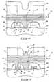
- FIG. 22With respect to a wafer fragment 10 c.
- a pair of finned capacitors 50 a and 50 care shown separated by a spacing “s”, which can be less than the minimum available photolithographic feature size.
- FIG. 17is the same as FIG. 6, but for provision of an additional masking layer 70 over first masking layer 34 .
- Layer 70is preferably provided where layers 30 and 34 constitute the same material, as will be apparent from FIG. 18 .
- anisotropic etching of second masking layer 36has occurred to form second opening 39 , with subsequent etching of layers 30 and 32 having been conducted to extend such opening to node 28 .
- layer 34remains in place with additional masking layer 70 restricting etching of layer 34 is while layers 30 are being etched.
- a conductive plugging layer 44 bis deposited.
- layer 44 bis etched or planarized back as shown, and masking layers 70 and 34 also etched.
- layers 30 and 32are etched to define the capacitor outline, with plugging material 44 b also being etched in the process where it is provided to be the same material as layers 32 .
- the unmasked first masking layeris etched after extending the second opening to the node where in the first described embodiment it is conducted before.
Landscapes
- Semiconductor Integrated Circuits (AREA)
- Semiconductor Memories (AREA)
Abstract
Description
Claims (7)
Priority Applications (1)
| Application Number | Priority Date | Filing Date | Title |
|---|---|---|---|
| US09/876,102US6762450B2 (en) | 1996-01-03 | 2001-06-06 | Method of forming a capacitor and a capacitor construction |
Applications Claiming Priority (3)
| Application Number | Priority Date | Filing Date | Title |
|---|---|---|---|
| US08/582,385US6218237B1 (en) | 1996-01-03 | 1996-01-03 | Method of forming a capacitor |
| US08/886,388US6900496B1 (en) | 1996-01-03 | 1997-07-01 | Capacitor constructions |
| US09/876,102US6762450B2 (en) | 1996-01-03 | 2001-06-06 | Method of forming a capacitor and a capacitor construction |
Related Parent Applications (1)
| Application Number | Title | Priority Date | Filing Date |
|---|---|---|---|
| US08/886,388ContinuationUS6900496B1 (en) | 1996-01-03 | 1997-07-01 | Capacitor constructions |
Publications (2)
| Publication Number | Publication Date |
|---|---|
| US20010030339A1 US20010030339A1 (en) | 2001-10-18 |
| US6762450B2true US6762450B2 (en) | 2004-07-13 |
Family
ID=24328946
Family Applications (4)
| Application Number | Title | Priority Date | Filing Date |
|---|---|---|---|
| US08/582,385Expired - LifetimeUS6218237B1 (en) | 1996-01-03 | 1996-01-03 | Method of forming a capacitor |
| US08/886,388Expired - Fee RelatedUS6900496B1 (en) | 1996-01-03 | 1997-07-01 | Capacitor constructions |
| US09/779,219Expired - LifetimeUS6395602B2 (en) | 1996-01-03 | 2001-02-07 | Method of forming a capacitor |
| US09/876,102Expired - Fee RelatedUS6762450B2 (en) | 1996-01-03 | 2001-06-06 | Method of forming a capacitor and a capacitor construction |
Family Applications Before (3)
| Application Number | Title | Priority Date | Filing Date |
|---|---|---|---|
| US08/582,385Expired - LifetimeUS6218237B1 (en) | 1996-01-03 | 1996-01-03 | Method of forming a capacitor |
| US08/886,388Expired - Fee RelatedUS6900496B1 (en) | 1996-01-03 | 1997-07-01 | Capacitor constructions |
| US09/779,219Expired - LifetimeUS6395602B2 (en) | 1996-01-03 | 2001-02-07 | Method of forming a capacitor |
Country Status (1)
| Country | Link |
|---|---|
| US (4) | US6218237B1 (en) |
Cited By (2)
| Publication number | Priority date | Publication date | Assignee | Title |
|---|---|---|---|---|
| US8564039B2 (en) | 2010-04-07 | 2013-10-22 | Micron Technology, Inc. | Semiconductor devices including gate structures comprising colossal magnetocapacitive materials |
| US9589726B2 (en) | 2013-10-01 | 2017-03-07 | E1023 Corporation | Magnetically enhanced energy storage systems and methods |
Families Citing this family (21)
| Publication number | Priority date | Publication date | Assignee | Title |
|---|---|---|---|---|
| US6238971B1 (en)* | 1997-02-11 | 2001-05-29 | Micron Technology, Inc. | Capacitor structures, DRAM cell structures, and integrated circuitry, and methods of forming capacitor structures, integrated circuitry and DRAM cell structures |
| US5905280A (en) | 1997-02-11 | 1999-05-18 | Micron Technology, Inc. | Capacitor structures, DRAM cell structures, methods of forming capacitors, methods of forming DRAM cells, and integrated circuits incorporating capacitor structures and DRAM cell structures |
| US5981333A (en) | 1997-02-11 | 1999-11-09 | Micron Technology, Inc. | Methods of forming capacitors and DRAM arrays |
| US5998257A (en) | 1997-03-13 | 1999-12-07 | Micron Technology, Inc. | Semiconductor processing methods of forming integrated circuitry memory devices, methods of forming capacitor containers, methods of making electrical connection to circuit nodes and related integrated circuitry |
| US6344392B1 (en)* | 1998-11-16 | 2002-02-05 | Vanguard International Semiconductor Corporation | Methods of manufacture of crown or stack capacitor with a monolithic fin structure made with a different oxide etching rate in hydrogen fluoride vapor |
| US6303956B1 (en)* | 1999-02-26 | 2001-10-16 | Micron Technology, Inc. | Conductive container structures having a dielectric cap |
| KR100343221B1 (en)* | 1999-11-09 | 2002-07-10 | 윤종용 | cooling device with cooling fin of micro structure |
| US7035864B1 (en)* | 2000-05-18 | 2006-04-25 | Endeca Technologies, Inc. | Hierarchical data-driven navigation system and method for information retrieval |
| KR100455724B1 (en) | 2001-10-08 | 2004-11-12 | 주식회사 하이닉스반도체 | Method for forming plug in semiconductor device |
| KR100491420B1 (en)* | 2002-11-06 | 2005-05-25 | 매그나칩 반도체 유한회사 | Method of forming a capacitor in a semiconductor device |
| US7105431B2 (en)* | 2003-08-22 | 2006-09-12 | Micron Technology, Inc. | Masking methods |
| US7354631B2 (en) | 2003-11-06 | 2008-04-08 | Micron Technology, Inc. | Chemical vapor deposition apparatus and methods |
| US7115524B2 (en)* | 2004-05-17 | 2006-10-03 | Micron Technology, Inc. | Methods of processing a semiconductor substrate |
| US7922769B2 (en) | 2004-09-27 | 2011-04-12 | Depuy Products, Inc. | Modular glenoid prosthesis and associated method |
| US7927335B2 (en) | 2004-09-27 | 2011-04-19 | Depuy Products, Inc. | Instrument for preparing an implant support surface and associated method |
| US7892287B2 (en) | 2004-09-27 | 2011-02-22 | Depuy Products, Inc. | Glenoid augment and associated method |
| US7371361B2 (en)* | 2004-11-03 | 2008-05-13 | Kellogg Brown & Root Llc | Maximum reaction rate converter system for exothermic reactions |
| KR100724568B1 (en)* | 2005-10-12 | 2007-06-04 | 삼성전자주식회사 | Semiconductor memory device and manufacturing method thereof |
| US8241365B2 (en)* | 2008-12-23 | 2012-08-14 | Depuy Products, Inc. | Shoulder prosthesis with vault-filling structure having bone-sparing configuration |
| US8231683B2 (en) | 2009-12-08 | 2012-07-31 | Depuy Products, Inc. | Shoulder prosthesis assembly having glenoid rim replacement structure |
| US8465548B2 (en) | 2010-11-24 | 2013-06-18 | DePuy Synthes Products, LLC | Modular glenoid prosthesis |
Citations (43)
| Publication number | Priority date | Publication date | Assignee | Title |
|---|---|---|---|---|
| US4558509A (en) | 1984-06-29 | 1985-12-17 | International Business Machines Corporation | Method for fabricating a gallium arsenide semiconductor device |
| US4568565A (en) | 1984-05-14 | 1986-02-04 | Allied Corporation | Light induced chemical vapor deposition of conductive titanium silicide films |
| US4742018A (en) | 1985-11-29 | 1988-05-03 | Hitachi, Ltd. | Process for producing memory cell having stacked capacitor |
| US5005072A (en) | 1990-01-29 | 1991-04-02 | Micron Technology, Inc. | Stacked cell design for 16-megabit DRAM array having a pair of interconnected poly layers which enfold a single field plate layer and connect to the cell's storage node junction |
| US5006481A (en) | 1989-11-30 | 1991-04-09 | Sgs-Thomson Microelectronics, Inc. | Method of making a stacked capacitor DRAM cell |
| US5021357A (en) | 1987-06-17 | 1991-06-04 | Fujitsu Limited | Method of making a dram cell with stacked capacitor |
| US5023683A (en) | 1988-09-30 | 1991-06-11 | Kabushiki Kaisha Toshiba | Semiconductor memory device with pillar-shaped insulating film |
| US5053351A (en) | 1991-03-19 | 1991-10-01 | Micron Technology, Inc. | Method of making stacked E-cell capacitor DRAM cell |
| US5061651A (en) | 1987-12-11 | 1991-10-29 | Oki Electric Industry Co., Ltd. | Method of making dram cell with stacked capacitor |
| US5071781A (en) | 1990-06-02 | 1991-12-10 | Samsung Electronics Co., Ltd. | Method for manufacturing a semiconductor |
| US5103275A (en) | 1989-11-30 | 1992-04-07 | Sharp Kabushiki Kaisha | Semiconductor memory |
| US5116776A (en) | 1989-11-30 | 1992-05-26 | Sgs-Thomson Microelectronics, Inc. | Method of making a stacked copacitor for dram cell |
| US5130172A (en) | 1988-10-21 | 1992-07-14 | The Regents Of The University Of California | Low temperature organometallic deposition of metals |
| US5135883A (en) | 1990-06-29 | 1992-08-04 | Samsung Electronics Co., Ltd. | Process for producing a stacked capacitor of a dram cell |
| US5139825A (en) | 1989-11-30 | 1992-08-18 | President And Fellows Of Harvard College | Process for chemical vapor deposition of transition metal nitrides |
| US5160987A (en) | 1989-10-26 | 1992-11-03 | International Business Machines Corporation | Three-dimensional semiconductor structures formed from planar layers |
| US5164337A (en) | 1989-11-01 | 1992-11-17 | Matsushita Electric Industrial Co., Ltd. | Method of fabricating a semiconductor device having a capacitor in a stacked memory cell |
| US5168073A (en) | 1991-10-31 | 1992-12-01 | Micron Technology, Inc. | Method for fabricating storage node capacitor having tungsten and etched tin storage node capacitor plate |
| US5170233A (en) | 1991-03-19 | 1992-12-08 | Micron Technology, Inc. | Method for increasing capacitive surface area of a conductive material in semiconductor processing and stacked memory cell capacitor |
| US5216267A (en) | 1989-05-10 | 1993-06-01 | Samsung Electronics Co., Ltd. | Stacked capacitor dynamic random access memory with a sloped lower electrode |
| US5223729A (en) | 1990-09-26 | 1993-06-29 | Matsushita Electric Industrial Co., Ltd. | Semiconductor device and a method of producing the same |
| US5290726A (en) | 1991-02-18 | 1994-03-01 | Goldstar Electron Co., Ltd. | DRAM cells having stacked capacitors of fin structures and method of making thereof |
| US5300321A (en) | 1992-05-12 | 1994-04-05 | Kawasaki Steel Corporation | Process for depositing titanium nitride film by CVD |
| US5320878A (en) | 1992-01-10 | 1994-06-14 | Martin Marietta Energy Systems, Inc. | Method of chemical vapor deposition of boron nitride using polymeric cyanoborane |
| US5330614A (en) | 1991-08-31 | 1994-07-19 | Samsung Electronics Co., Ltd. | Manufacturing method of a capacitor having a storage electrode whose sidewall is positively inclined with respect to the horizontal surface |
| US5403620A (en) | 1992-10-13 | 1995-04-04 | Regents Of The University Of California | Catalysis in organometallic CVD of thin metal films |
| US5444010A (en) | 1993-05-13 | 1995-08-22 | Hyundai Electronics Industries, Ltd. | Method for forming a stacked capacitor in a semiconductor device |
| US5464786A (en) | 1994-10-24 | 1995-11-07 | Micron Technology, Inc. | Method for forming a capacitor having recessed lateral reaction barrier layer edges |
| US5508218A (en) | 1993-12-28 | 1996-04-16 | Lg Semicon Co., Ltd. | Method for fabricating a semiconductor memory |
| US5622882A (en) | 1994-12-30 | 1997-04-22 | Lsi Logic Corporation | Method of making a CMOS dynamic random-access memory (DRAM) |
| US5631184A (en) | 1992-03-13 | 1997-05-20 | Fujitsu Limited | Method of producing a semiconductor device having a fin type capacitor |
| US5677222A (en) | 1996-10-11 | 1997-10-14 | Vanguard International Semiconductor Corporation | Method for forming a DRAM capacitor |
| US5684316A (en)* | 1994-05-13 | 1997-11-04 | Samsung Electronics Co., Ltd. | Semiconductor memory device provided with capacitors formed above and below a cell transistor |
| US5907170A (en) | 1997-10-06 | 1999-05-25 | Micron Technology, Inc. | Circuit and method for an open bit line memory cell with a vertical transistor and trench plate trench capacitor |
| US5930640A (en) | 1995-06-07 | 1999-07-27 | International Business Machines Corporation | Mechanical supports for very thin stacked capacitor plates |
| US5945704A (en) | 1998-04-06 | 1999-08-31 | Siemens Aktiengesellschaft | Trench capacitor with epi buried layer |
| US5953254A (en) | 1996-09-09 | 1999-09-14 | Azalea Microelectronics Corp. | Serial flash memory |
| US5952688A (en) | 1992-07-23 | 1999-09-14 | Texas Instruments Incorporated | Stacked DRAM structure |
| US5968686A (en) | 1996-08-15 | 1999-10-19 | Nec Corporation | Charged-beam exposure mask and charged-beam exposure method |
| US6025248A (en) | 1997-10-07 | 2000-02-15 | Samsung Electronics Co., Ltd. | Methods of forming capacitor electrodes including a capacitor electrode etch |
| US6025624A (en) | 1998-06-19 | 2000-02-15 | Micron Technology, Inc. | Shared length cell for improved capacitance |
| US6037620A (en) | 1998-06-08 | 2000-03-14 | International Business Machines Corporation | DRAM cell with transfer device extending along perimeter of trench storage capacitor |
| US6150687A (en) | 1997-07-08 | 2000-11-21 | Micron Technology, Inc. | Memory cell having a vertical transistor with buried source/drain and dual gates |
Family Cites Families (2)
| Publication number | Priority date | Publication date | Assignee | Title |
|---|---|---|---|---|
| US5573967A (en)* | 1991-12-20 | 1996-11-12 | Industrial Technology Research Institute | Method for making dynamic random access memory with fin-type stacked capacitor |
| US5383088A (en)* | 1993-08-09 | 1995-01-17 | International Business Machines Corporation | Storage capacitor with a conducting oxide electrode for metal-oxide dielectrics |
- 1996
- 1996-01-03USUS08/582,385patent/US6218237B1/ennot_activeExpired - Lifetime
- 1997
- 1997-07-01USUS08/886,388patent/US6900496B1/ennot_activeExpired - Fee Related
- 2001
- 2001-02-07USUS09/779,219patent/US6395602B2/ennot_activeExpired - Lifetime
- 2001-06-06USUS09/876,102patent/US6762450B2/ennot_activeExpired - Fee Related
Patent Citations (43)
| Publication number | Priority date | Publication date | Assignee | Title |
|---|---|---|---|---|
| US4568565A (en) | 1984-05-14 | 1986-02-04 | Allied Corporation | Light induced chemical vapor deposition of conductive titanium silicide films |
| US4558509A (en) | 1984-06-29 | 1985-12-17 | International Business Machines Corporation | Method for fabricating a gallium arsenide semiconductor device |
| US4742018A (en) | 1985-11-29 | 1988-05-03 | Hitachi, Ltd. | Process for producing memory cell having stacked capacitor |
| US5021357A (en) | 1987-06-17 | 1991-06-04 | Fujitsu Limited | Method of making a dram cell with stacked capacitor |
| US5061651A (en) | 1987-12-11 | 1991-10-29 | Oki Electric Industry Co., Ltd. | Method of making dram cell with stacked capacitor |
| US5023683A (en) | 1988-09-30 | 1991-06-11 | Kabushiki Kaisha Toshiba | Semiconductor memory device with pillar-shaped insulating film |
| US5130172A (en) | 1988-10-21 | 1992-07-14 | The Regents Of The University Of California | Low temperature organometallic deposition of metals |
| US5216267A (en) | 1989-05-10 | 1993-06-01 | Samsung Electronics Co., Ltd. | Stacked capacitor dynamic random access memory with a sloped lower electrode |
| US5160987A (en) | 1989-10-26 | 1992-11-03 | International Business Machines Corporation | Three-dimensional semiconductor structures formed from planar layers |
| US5164337A (en) | 1989-11-01 | 1992-11-17 | Matsushita Electric Industrial Co., Ltd. | Method of fabricating a semiconductor device having a capacitor in a stacked memory cell |
| US5006481A (en) | 1989-11-30 | 1991-04-09 | Sgs-Thomson Microelectronics, Inc. | Method of making a stacked capacitor DRAM cell |
| US5103275A (en) | 1989-11-30 | 1992-04-07 | Sharp Kabushiki Kaisha | Semiconductor memory |
| US5116776A (en) | 1989-11-30 | 1992-05-26 | Sgs-Thomson Microelectronics, Inc. | Method of making a stacked copacitor for dram cell |
| US5139825A (en) | 1989-11-30 | 1992-08-18 | President And Fellows Of Harvard College | Process for chemical vapor deposition of transition metal nitrides |
| US5005072A (en) | 1990-01-29 | 1991-04-02 | Micron Technology, Inc. | Stacked cell design for 16-megabit DRAM array having a pair of interconnected poly layers which enfold a single field plate layer and connect to the cell's storage node junction |
| US5071781A (en) | 1990-06-02 | 1991-12-10 | Samsung Electronics Co., Ltd. | Method for manufacturing a semiconductor |
| US5135883A (en) | 1990-06-29 | 1992-08-04 | Samsung Electronics Co., Ltd. | Process for producing a stacked capacitor of a dram cell |
| US5223729A (en) | 1990-09-26 | 1993-06-29 | Matsushita Electric Industrial Co., Ltd. | Semiconductor device and a method of producing the same |
| US5290726A (en) | 1991-02-18 | 1994-03-01 | Goldstar Electron Co., Ltd. | DRAM cells having stacked capacitors of fin structures and method of making thereof |
| US5053351A (en) | 1991-03-19 | 1991-10-01 | Micron Technology, Inc. | Method of making stacked E-cell capacitor DRAM cell |
| US5170233A (en) | 1991-03-19 | 1992-12-08 | Micron Technology, Inc. | Method for increasing capacitive surface area of a conductive material in semiconductor processing and stacked memory cell capacitor |
| US5330614A (en) | 1991-08-31 | 1994-07-19 | Samsung Electronics Co., Ltd. | Manufacturing method of a capacitor having a storage electrode whose sidewall is positively inclined with respect to the horizontal surface |
| US5168073A (en) | 1991-10-31 | 1992-12-01 | Micron Technology, Inc. | Method for fabricating storage node capacitor having tungsten and etched tin storage node capacitor plate |
| US5320878A (en) | 1992-01-10 | 1994-06-14 | Martin Marietta Energy Systems, Inc. | Method of chemical vapor deposition of boron nitride using polymeric cyanoborane |
| US5631184A (en) | 1992-03-13 | 1997-05-20 | Fujitsu Limited | Method of producing a semiconductor device having a fin type capacitor |
| US5300321A (en) | 1992-05-12 | 1994-04-05 | Kawasaki Steel Corporation | Process for depositing titanium nitride film by CVD |
| US5952688A (en) | 1992-07-23 | 1999-09-14 | Texas Instruments Incorporated | Stacked DRAM structure |
| US5403620A (en) | 1992-10-13 | 1995-04-04 | Regents Of The University Of California | Catalysis in organometallic CVD of thin metal films |
| US5444010A (en) | 1993-05-13 | 1995-08-22 | Hyundai Electronics Industries, Ltd. | Method for forming a stacked capacitor in a semiconductor device |
| US5508218A (en) | 1993-12-28 | 1996-04-16 | Lg Semicon Co., Ltd. | Method for fabricating a semiconductor memory |
| US5684316A (en)* | 1994-05-13 | 1997-11-04 | Samsung Electronics Co., Ltd. | Semiconductor memory device provided with capacitors formed above and below a cell transistor |
| US5464786A (en) | 1994-10-24 | 1995-11-07 | Micron Technology, Inc. | Method for forming a capacitor having recessed lateral reaction barrier layer edges |
| US5622882A (en) | 1994-12-30 | 1997-04-22 | Lsi Logic Corporation | Method of making a CMOS dynamic random-access memory (DRAM) |
| US5930640A (en) | 1995-06-07 | 1999-07-27 | International Business Machines Corporation | Mechanical supports for very thin stacked capacitor plates |
| US5968686A (en) | 1996-08-15 | 1999-10-19 | Nec Corporation | Charged-beam exposure mask and charged-beam exposure method |
| US5953254A (en) | 1996-09-09 | 1999-09-14 | Azalea Microelectronics Corp. | Serial flash memory |
| US5677222A (en) | 1996-10-11 | 1997-10-14 | Vanguard International Semiconductor Corporation | Method for forming a DRAM capacitor |
| US6150687A (en) | 1997-07-08 | 2000-11-21 | Micron Technology, Inc. | Memory cell having a vertical transistor with buried source/drain and dual gates |
| US5907170A (en) | 1997-10-06 | 1999-05-25 | Micron Technology, Inc. | Circuit and method for an open bit line memory cell with a vertical transistor and trench plate trench capacitor |
| US6025248A (en) | 1997-10-07 | 2000-02-15 | Samsung Electronics Co., Ltd. | Methods of forming capacitor electrodes including a capacitor electrode etch |
| US5945704A (en) | 1998-04-06 | 1999-08-31 | Siemens Aktiengesellschaft | Trench capacitor with epi buried layer |
| US6037620A (en) | 1998-06-08 | 2000-03-14 | International Business Machines Corporation | DRAM cell with transfer device extending along perimeter of trench storage capacitor |
| US6025624A (en) | 1998-06-19 | 2000-02-15 | Micron Technology, Inc. | Shared length cell for improved capacitance |
Non-Patent Citations (9)
| Title |
|---|
| Conrad, J.R. et al., "Ion Beam Assisted Conring And Surface Modification With Plasma Source Ion Implantation". J. Vac, Sci. Technol. A B (4), Jul./Aug. 1990, 3146-3151. |
| Ema, T. et al., "3-Dimensional Stacked Capacitor Cell for 16M And 64M DRAMs," MOS Division, Fujitsu Limited, IEEE 1988, pp. 592-595. |
| H. Wannabe et al., "Stacked Capacitor Cells for High-density dynamic RAM's", IEDM 1988, pp. 600-603. |
| Inouc. S., et al., "A Spread Stacked Capacitor (SCC) Cell for 64MBIT DRAMs", IEEE 1989, pp. 31-34 (23.1-23.4). |
| Nierdef, H., et al., "Organometallic Chemical Vapor Deposition of Tungsten Metal, and Suppression of Carbon Incorporation by Codeposition of Platinum", Article, University of California, Los Angeles, CA, Dept. of Chemistry and Biochemistry, published Aug. 4, 1992. 3 pp. |
| S. Woo et al., "Selective Etching Technology of in-situ P Doped Poly-Si (SEDOP) for High Density DRAM Capacitors", 1994 Symposium on VLSI Technology Digest of Technical Papers, pp. 25-26. |
| T. Morihara et al., "Disk-Shaped Stacked Capacitor Cell for 256 Mb Dynamic Random-Access Memory", Aug. 19, 1994, Jpn. J. Appl. Phys. vol. 33 (1994), Pt. 1, No. 8, pp. 14-19. |
| Temmter, D. "Multilayer Vertical Stacked Capactors (MVSTC) for 64 Mbit and 256 mBit DRAMs", Article, Institute of Semiconducter Physics, Germany, no date, 2 pgs. |
| Wolf, S. et al., "Silicon Processing for the VLSI Ern," 1986, Lattica Press, p. 493. |
Cited By (4)
| Publication number | Priority date | Publication date | Assignee | Title |
|---|---|---|---|---|
| US8564039B2 (en) | 2010-04-07 | 2013-10-22 | Micron Technology, Inc. | Semiconductor devices including gate structures comprising colossal magnetocapacitive materials |
| US9245923B2 (en) | 2010-04-07 | 2016-01-26 | Micron Technology, Inc. | Method of fabricating a semiconductor device having a colossal magneto-capacitive material being formed close to a channel region of a transistor |
| US9589726B2 (en) | 2013-10-01 | 2017-03-07 | E1023 Corporation | Magnetically enhanced energy storage systems and methods |
| US10176928B2 (en) | 2013-10-01 | 2019-01-08 | E1023 Corporation | Magnetically enhanced energy storage systems |
Also Published As
| Publication number | Publication date |
|---|---|
| US6900496B1 (en) | 2005-05-31 |
| US6218237B1 (en) | 2001-04-17 |
| US20010030339A1 (en) | 2001-10-18 |
| US6395602B2 (en) | 2002-05-28 |
| US20010009286A1 (en) | 2001-07-26 |
Similar Documents
| Publication | Publication Date | Title |
|---|---|---|
| US6762450B2 (en) | Method of forming a capacitor and a capacitor construction | |
| US6300213B1 (en) | Semiconductor processing methods of forming a storage node of a capacitor | |
| US5604147A (en) | Method of forming a cylindrical container stacked capacitor | |
| KR940006682B1 (en) | Manufacturing Method of Semiconductor Memory Device | |
| US6624018B1 (en) | Method of fabricating a DRAM device featuring alternate fin type capacitor structures | |
| US6184081B1 (en) | Method of fabricating a capacitor under bit line DRAM structure using contact hole liners | |
| US6153527A (en) | Semiconductor processing method of making electrical contact to a node received within a mass of insulating dielectric material | |
| US6100137A (en) | Etch stop layer used for the fabrication of an overlying crown shaped storage node structure | |
| US6468858B1 (en) | Method of forming a metal insulator metal capacitor structure | |
| US6187621B1 (en) | Semiconductor processing methods of forming capacitor constructions and semiconductor processing methods of forming DRAM constructions | |
| US6548348B1 (en) | Method of forming a storage node contact hole in a porous insulator layer | |
| US6417066B1 (en) | Method of forming a DRAM capacitor structure including increasing the surface area using a discrete silicon mask | |
| US6143605A (en) | Method for making a DRAM capacitor using a double layer of insitu doped polysilicon and undoped amorphous polysilicon with HSG polysilicon | |
| US6054347A (en) | Method for forming a modified crown shaped, dynamic random access memory, (DRAM), capacitor structure | |
| US5792688A (en) | Method to increase the surface area of a storage node electrode, of an STC structure, for DRAM devices, via formation of polysilicon columns | |
| US6214687B1 (en) | Method of forming a capacitor and a capacitor construction | |
| US5710074A (en) | Increased surface area of an STC structure via the use of a storage node electrode comprised of polysilicon mesas and polysilicon sidewall spacers | |
| US6580112B2 (en) | Method for fabricating an open can-type stacked capacitor on an uneven surface | |
| US6235580B1 (en) | Process for forming a crown shaped capacitor structure for a DRAM device | |
| US6400022B1 (en) | Semiconductor device and fabrication process therefor and capacitor structure | |
| KR960015526B1 (en) | Semiconductor device and manufacturing method | |
| KR100384793B1 (en) | Method for manufacturing capacitor | |
| KR0132856B1 (en) | Capacitor of Semiconductor Device and Manufacturing Method Thereof | |
| KR100380279B1 (en) | Method for fabricating capacitor | |
| KR20010003745A (en) | Method of manufacturing semiconductor memory device |
Legal Events
| Date | Code | Title | Description |
|---|---|---|---|
| FEPP | Fee payment procedure | Free format text:PAYOR NUMBER ASSIGNED (ORIGINAL EVENT CODE: ASPN); ENTITY STATUS OF PATENT OWNER: LARGE ENTITY | |
| CC | Certificate of correction | ||
| FPAY | Fee payment | Year of fee payment:4 | |
| AS | Assignment | Owner name:MOSAID TECHNOLOGIES INCORPORATED, CANADA Free format text:ASSIGNMENT OF ASSIGNORS INTEREST;ASSIGNOR:MICRON TECHNOLOGY, INC.;REEL/FRAME:023220/0243 Effective date:20090609 | |
| AS | Assignment | Owner name:MOSAID TECHNOLOGIES INCORPORATED,CANADA Free format text:CORRECTIVE ASSIGNMENT TO CORRECT THE TO CORRECT THE ASSIGNEES' ADDRESS PREVIOUSLY RECORDED ON REEL 023220 FRAME 0243. ASSIGNOR(S) HEREBY CONFIRMS THE MOSAID TECHNOLOGIES INCORPORATED 6 SAUBLE DRIVE, SUITE 203, OTTAWA,ONTARIO, CANADA K2K 2X1;ASSIGNOR:MICRON TECHNOLOGY, INC.;REEL/FRAME:024225/0878 Effective date:20090609 | |
| FPAY | Fee payment | Year of fee payment:8 | |
| AS | Assignment | Owner name:ROYAL BANK OF CANADA, CANADA Free format text:U.S. INTELLECTUAL PROPERTY SECURITY AGREEMENT (FOR NON-U.S. GRANTORS) - SHORT FORM;ASSIGNORS:658276 N.B. LTD.;658868 N.B. INC.;MOSAID TECHNOLOGIES INCORPORATED;REEL/FRAME:027512/0196 Effective date:20111223 | |
| AS | Assignment | Owner name:CONVERSANT INTELLECTUAL PROPERTY MANAGEMENT INC., Free format text:CHANGE OF NAME;ASSIGNOR:MOSAID TECHNOLOGIES INCORPORATED;REEL/FRAME:032439/0638 Effective date:20140101 | |
| AS | Assignment | Owner name:CONVERSANT IP N.B. 868 INC., CANADA Free format text:RELEASE OF SECURITY INTEREST;ASSIGNOR:ROYAL BANK OF CANADA;REEL/FRAME:033484/0344 Effective date:20140611 Owner name:CONVERSANT INTELLECTUAL PROPERTY MANAGEMENT INC., Free format text:RELEASE OF SECURITY INTEREST;ASSIGNOR:ROYAL BANK OF CANADA;REEL/FRAME:033484/0344 Effective date:20140611 Owner name:CONVERSANT IP N.B. 276 INC., CANADA Free format text:RELEASE OF SECURITY INTEREST;ASSIGNOR:ROYAL BANK OF CANADA;REEL/FRAME:033484/0344 Effective date:20140611 | |
| AS | Assignment | Owner name:CONVERSANT INTELLECTUAL PROPERTY MANAGEMENT INC., CANADA Free format text:CHANGE OF ADDRESS;ASSIGNOR:CONVERSANT INTELLECTUAL PROPERTY MANAGEMENT INC.;REEL/FRAME:033678/0096 Effective date:20140820 Owner name:CONVERSANT INTELLECTUAL PROPERTY MANAGEMENT INC., Free format text:CHANGE OF ADDRESS;ASSIGNOR:CONVERSANT INTELLECTUAL PROPERTY MANAGEMENT INC.;REEL/FRAME:033678/0096 Effective date:20140820 | |
| AS | Assignment | Owner name:ROYAL BANK OF CANADA, AS LENDER, CANADA Free format text:U.S. PATENT SECURITY AGREEMENT (FOR NON-U.S. GRANTORS);ASSIGNOR:CONVERSANT INTELLECTUAL PROPERTY MANAGEMENT INC.;REEL/FRAME:033706/0367 Effective date:20140611 Owner name:CPPIB CREDIT INVESTMENTS INC., AS LENDER, CANADA Free format text:U.S. PATENT SECURITY AGREEMENT (FOR NON-U.S. GRANTORS);ASSIGNOR:CONVERSANT INTELLECTUAL PROPERTY MANAGEMENT INC.;REEL/FRAME:033706/0367 Effective date:20140611 | |
| REMI | Maintenance fee reminder mailed | ||
| LAPS | Lapse for failure to pay maintenance fees | ||
| STCH | Information on status: patent discontinuation | Free format text:PATENT EXPIRED DUE TO NONPAYMENT OF MAINTENANCE FEES UNDER 37 CFR 1.362 | |
| FP | Lapsed due to failure to pay maintenance fee | Effective date:20160713 | |
| AS | Assignment | Owner name:CONVERSANT INTELLECTUAL PROPERTY MANAGEMENT INC., CANADA Free format text:RELEASE OF U.S. PATENT AGREEMENT (FOR NON-U.S. GRANTORS);ASSIGNOR:ROYAL BANK OF CANADA, AS LENDER;REEL/FRAME:047645/0424 Effective date:20180731 Owner name:CONVERSANT INTELLECTUAL PROPERTY MANAGEMENT INC., Free format text:RELEASE OF U.S. PATENT AGREEMENT (FOR NON-U.S. GRANTORS);ASSIGNOR:ROYAL BANK OF CANADA, AS LENDER;REEL/FRAME:047645/0424 Effective date:20180731 |