US6762434B2 - Electrical print resolution test die - Google Patents
Electrical print resolution test dieDownload PDFInfo
- Publication number
- US6762434B2 US6762434B2US10/422,165US42216503AUS6762434B2US 6762434 B2US6762434 B2US 6762434B2US 42216503 AUS42216503 AUS 42216503AUS 6762434 B2US6762434 B2US 6762434B2
- Authority
- US
- United States
- Prior art keywords
- metal
- comb
- tines
- serpentine
- line
- Prior art date
- Legal status (The legal status is an assumption and is not a legal conclusion. Google has not performed a legal analysis and makes no representation as to the accuracy of the status listed.)
- Expired - Lifetime
Links
Images


Classifications
- H—ELECTRICITY
- H01—ELECTRIC ELEMENTS
- H01L—SEMICONDUCTOR DEVICES NOT COVERED BY CLASS H10
- H01L22/00—Testing or measuring during manufacture or treatment; Reliability measurements, i.e. testing of parts without further processing to modify the parts as such; Structural arrangements therefor
- H01L22/30—Structural arrangements specially adapted for testing or measuring during manufacture or treatment, or specially adapted for reliability measurements
- H01L22/34—Circuits for electrically characterising or monitoring manufacturing processes, e. g. whole test die, wafers filled with test structures, on-board-devices incorporated on each die, process control monitors or pad structures thereof, devices in scribe line
Definitions
- This inventionrelates to test structures used in semiconductor manufacturing, and in particular to test structures used to determine the print quality and resolution of in a lithographic process.
- Photomasksare an integral component in the lithographic process of semiconductor manufacturing. Semiconductor manufacturers use photomasks to optically transfer (e.g., print) images of devices (e.g., integrated circuits) onto semiconductor wafers.
- a lithography tool called stepperprojects light through the photomask to print the image of one or more devices onto a field on a silicon wafer coated with photoresist. The stepper then moves (e.g., steps) the wafer and the image is exposed once again onto another field on the wafer. This process is repeated for the entire wafer surface.
- the exposed portions of the photoresistare removed so areas of the wafer underneath can either be etched to form channels or be deposited with other materials. This process can be reversed using a negative photoresist where the unexposed portions of the photoresist are removed.
- Print resolutionis the smallest line and space that can be precisely printed (matching the mask dimension.) Print resolution depends predominately on the focus of the stepper, but could also depend on various other factors. For example, if the stepper is not able to print one micron at a particular time, then the stepper cannot be used to produce one micron devices until maintenance and repair are performed.
- a test structure patternincludes a first comb, a second comb, and a serpentine line.
- the first combincludes a first set of tines of the same orientation.
- the second combincludes a second set of tines of the same orientation that are interdigitated with the first set of tines.
- the serpentine lineruns between the interdigitated tines of the first comb and the second comb.
- the test structure patternforms a first metal comb, a second metal comb, and a serpentine metal line on a die.
- electrical continuityis checked on the serpentine metal line. If a current cannot flow through in the serpentine metal line, then the serpentine metal line is broken or discontinuous. This suggests the resolution of the stepper is compromised due to being overexposed or out of focus.
- electrical continuityis also checked between the serpentine metal line and at least the first metal comb and/or the second metal comb. If a current can flow between the serpentine metal line and either the first metal comb or the second metal comb, then this implies there is bridging across a gap where there should not be any conductance. This suggests the resolution of the stepper is compromised due to being underexposed or out of focus.
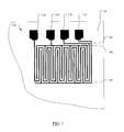
- FIG. 1illustrates a test structure pattern for electrically detecting the print quality and resolution of a lithographic process in one embodiment of the invention.
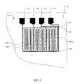
- FIG. 2illustrates the test structure pattern of FIG. 1 where an upper comb is shown with dashed lines.
- FIG. 3illustrates the test structure pattern of FIG. 1 where a lower comb is shown with dashed lines.
- FIG. 4illustrates the test structure pattern of FIG. 1 where a serpentine line is shown with a dashed line.
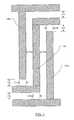
- FIG. 5illustrates an enlarge view of a part of the serpentine line, a tine of the upper comb, and a tine of the lower comb in one embodiment of the invention.
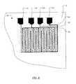
- FIG. 6illustrates a test die formed from the test structure pattern of FIG. 1 in one embodiment of the invention.
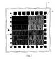
- FIG. 7illustrates multiple test structure patterns of FIG. 1 with decrementing critical dimensions on a photomask for electrically detecting the print quality and resolution of a lithographic process in one embodiment of the invention.
- FIG. 1illustrates a test structure pattern 100 on a photomask 10 used with positive (or negative) photoresist in one embodiment of the invention.
- Test structure pattern 100forms a test die 600 (FIG. 6) for electrically detecting the print quality and resolution in a lithographic process.
- Test structure pattern 100includes an upper comb 102 , a lower comb 104 , and a serpentine line 106 .
- Upper comb 102(as shown more clearly in FIG. 2 with dashed lines) includes a number of upper tines 108 - 1 , 108 - 2 , . . . , 108 -m (collectively as “upper tines 108 ”) all of the same orientation (e.g., vertical).
- Upper tines 108are coupled in parallel to a bond pad 110 .
- lower comb 104(as shown more clearly in FIG. 3 with dashed lines) includes a number of lower tines 112 - 1 , 112 - 2 , . . . , 112 -n (collectively as “lower tines 112 ”) all of the same orientation as upper tines 108 .
- Lower tines 112are coupled in parallel to a bond pad 114 .
- Lower tines 112are interdigitated with upper tines 108 .
- Serpentine line 106(as shown more clearly in FIG. 4 with a dashed line) runs back and forth between the interdigitated lower and upper tines. One end of line 106 is coupled to a bond pad 116 , and the other end of line 106 is coupled to a bond pad 118 .
- FIG. 5illustrates an exemplary cutout of test structure pattern 100 .
- serpentine line 106 , upper tines 108 , and lower tines 112are separated from each other by a critical dimension CD (except in the corner).
- Each of serpentine line 106 , upper tines 108 , and lower tines 112has a width of critical dimension CD.
- FIG. 6illustrates an exemplary a test die 600 formed from test structure pattern 100 printed on photoresist over a conductive layer on a wafer.
- the conductive layeris generally above a dielectric layer on the wafer.
- Test die 600includes a metal upper comb 602 with metal tines 608 , a metal lower comb 604 with metal tines 612 , a metal serpentine line 606 , and metal bond pads 110 , 114 , 116 , and 118 .
- test die 600is measured for continuity of metal line 606 , upper bridging between metal line 606 and upper comb 602 , and lower bridging between metal line 606 and lower comb 604 .
- an electrical currentis supplied to pad 616 and the current is checked at pads 610 , 614 , and 618 .
- metal line 606is not continuous. Metal line 606 is not continuous when the lithographic process is unable to print and/or etch metal line 606 with a width of critical dimension CD. Thus, metal line 606 becomes too narrow and breaks somewhere along its path. It is also possible too tell how much narrower the line is by comparing measured resistance values to known good samples with known metal thicknesses. Since the length is fixed then any change in resistance would be indicate a change in width (metal CD).
- metal line 606has contacted one or more of upper tines 608 .
- metal line 606has contacted one or more of lower tines 612 .
- Metal line 606contacts upper tines 608 or lower tines 612 when the lithographic process is unable to print and/or etch them with a width of critical dimension CD. Thus, one or more of metal line 606 , upper tines 608 , or lower tines 612 become too wide and they touch somewhere along their paths.
- FIG. 7illustrates that test structure pattern 100 can be repeated on photomask 10 with different decrementing critical dimension CDs.
- photomask 10printed on a single field to determine the smallest critical dimension CD produced by a specific lithographic process.
- Test structure pattern 100 with the interdigitated and serpentine patternsoffers a good test for print quality and resolution because the elements on the test die are densely packed.
- other test structureswith constant width and constant gap through a long path can also be used to test print quality and resolution.
- lines that form concentric circles, scrolling jet vanes, and twisting conical shellscan possibly be used in other test structures.
- the actual dimension CD of metal line 606can be determined.
- a resistance R of metal line 606 between metal pads 616 and 618can be determined from the voltage drop and the supplied current. Resistance R can be correlated for the type of the metal layer to the width, length, and thickness of metal line 606 .
- the length of metal line 606is measured during layout of the test die (during CAD).
- the thickness of metal line 606can be measured after metal deposition by using a V/I 4 point probe (or equivalent) that converts resistivity to thickness. If the length and the thickness are known, then the width of metal line 606 can be conventionally calculated.
- the sizes of bond pads 110 , 114 , 116 , and 118are varied. Measurements can be taken between each resulting metal bond pad and the substrate to qualify the capacitive quality of the dielectric layer between the metal layer and the substrate. Furthermore, if a current is detected between a metal bond pad and the substrate, then there are particles on the wafer. Thus, the bond pads can also be used for defect monitoring.
Landscapes
- Engineering & Computer Science (AREA)
- Manufacturing & Machinery (AREA)
- Automation & Control Theory (AREA)
- Computer Hardware Design (AREA)
- Microelectronics & Electronic Packaging (AREA)
- Power Engineering (AREA)
- Exposure And Positioning Against Photoresist Photosensitive Materials (AREA)
- Testing Or Measuring Of Semiconductors Or The Like (AREA)
Abstract
Description
Claims (3)
Priority Applications (1)
| Application Number | Priority Date | Filing Date | Title |
|---|---|---|---|
| US10/422,165US6762434B2 (en) | 2002-04-01 | 2003-04-23 | Electrical print resolution test die |
Applications Claiming Priority (2)
| Application Number | Priority Date | Filing Date | Title |
|---|---|---|---|
| US10/114,703US6649932B2 (en) | 2002-04-01 | 2002-04-01 | Electrical print resolution test die |
| US10/422,165US6762434B2 (en) | 2002-04-01 | 2003-04-23 | Electrical print resolution test die |
Related Parent Applications (1)
| Application Number | Title | Priority Date | Filing Date |
|---|---|---|---|
| US10/114,703DivisionUS6649932B2 (en) | 2002-04-01 | 2002-04-01 | Electrical print resolution test die |
Publications (2)
| Publication Number | Publication Date |
|---|---|
| US20030210058A1 US20030210058A1 (en) | 2003-11-13 |
| US6762434B2true US6762434B2 (en) | 2004-07-13 |
Family
ID=28453830
Family Applications (2)
| Application Number | Title | Priority Date | Filing Date |
|---|---|---|---|
| US10/114,703Expired - LifetimeUS6649932B2 (en) | 2002-04-01 | 2002-04-01 | Electrical print resolution test die |
| US10/422,165Expired - LifetimeUS6762434B2 (en) | 2002-04-01 | 2003-04-23 | Electrical print resolution test die |
Family Applications Before (1)
| Application Number | Title | Priority Date | Filing Date |
|---|---|---|---|
| US10/114,703Expired - LifetimeUS6649932B2 (en) | 2002-04-01 | 2002-04-01 | Electrical print resolution test die |
Country Status (1)
| Country | Link |
|---|---|
| US (2) | US6649932B2 (en) |
Cited By (3)
| Publication number | Priority date | Publication date | Assignee | Title |
|---|---|---|---|---|
| US7176675B1 (en) | 2005-11-29 | 2007-02-13 | International Business Machines Corporation | Proximity sensitive defect monitor |
| US20080088601A1 (en)* | 2004-05-19 | 2008-04-17 | Tpk Touch Solutions Inc. | Circuit layout on a touch panel |
| US7491476B1 (en) | 2008-04-16 | 2009-02-17 | International Business Machines Corporation | Photomask electrical monitor for production photomasks |
Families Citing this family (8)
| Publication number | Priority date | Publication date | Assignee | Title |
|---|---|---|---|---|
| US20070089540A1 (en)* | 2005-10-26 | 2007-04-26 | Motorola, Inc. | Method and apparatus to facilitate testing of printed semiconductor devices |
| US8519388B2 (en)* | 2007-12-17 | 2013-08-27 | Nxp B.V. | Embedded structure for passivation integrity testing |
| CN103367323B (en)* | 2012-03-31 | 2015-12-16 | 中芯国际集成电路制造(上海)有限公司 | Detect domain structure and detection method |
| CN104681429B (en)* | 2013-11-27 | 2017-12-29 | 中芯国际集成电路制造(上海)有限公司 | The forming method of semiconductor structure |
| CN104752254B (en)* | 2013-12-31 | 2017-08-25 | 中芯国际集成电路制造(上海)有限公司 | The forming method of test structure |
| CN108766957A (en)* | 2018-06-20 | 2018-11-06 | 上海华虹宏力半导体制造有限公司 | Semi-conductor test structure and semiconductor structure |
| KR102747247B1 (en)* | 2019-04-18 | 2024-12-31 | 삼성전자주식회사 | Pattern disign and method for inspecting the pattern disign |
| CN116679528A (en)* | 2023-06-25 | 2023-09-01 | 上海盛剑微电子有限公司 | Mask design method and mask |
Citations (4)
| Publication number | Priority date | Publication date | Assignee | Title |
|---|---|---|---|---|
| USRE37184E1 (en)* | 1991-11-20 | 2001-05-22 | Kabushiki Kaisha Toshiba | Semiconductor memory and screening test method thereof |
| US6429454B2 (en)* | 2000-06-12 | 2002-08-06 | Kabushiki Kaisha Toshiba | Semiconductor device with test circuit |
| US6483304B1 (en)* | 1997-03-13 | 2002-11-19 | Ricoh Company, Ltd. | Magnetic field probe having a shielding and isolating layers to protect lead wires extending between a coil and pads |
| US6492832B2 (en)* | 1999-07-02 | 2002-12-10 | Samsung Electronics Co., Ltd. | Methods for testing a group of semiconductor devices simultaneously, and devices amenable to such methods of testing |
- 2002
- 2002-04-01USUS10/114,703patent/US6649932B2/ennot_activeExpired - Lifetime
- 2003
- 2003-04-23USUS10/422,165patent/US6762434B2/ennot_activeExpired - Lifetime
Patent Citations (4)
| Publication number | Priority date | Publication date | Assignee | Title |
|---|---|---|---|---|
| USRE37184E1 (en)* | 1991-11-20 | 2001-05-22 | Kabushiki Kaisha Toshiba | Semiconductor memory and screening test method thereof |
| US6483304B1 (en)* | 1997-03-13 | 2002-11-19 | Ricoh Company, Ltd. | Magnetic field probe having a shielding and isolating layers to protect lead wires extending between a coil and pads |
| US6492832B2 (en)* | 1999-07-02 | 2002-12-10 | Samsung Electronics Co., Ltd. | Methods for testing a group of semiconductor devices simultaneously, and devices amenable to such methods of testing |
| US6429454B2 (en)* | 2000-06-12 | 2002-08-06 | Kabushiki Kaisha Toshiba | Semiconductor device with test circuit |
Cited By (5)
| Publication number | Priority date | Publication date | Assignee | Title |
|---|---|---|---|---|
| US20080088601A1 (en)* | 2004-05-19 | 2008-04-17 | Tpk Touch Solutions Inc. | Circuit layout on a touch panel |
| US7176675B1 (en) | 2005-11-29 | 2007-02-13 | International Business Machines Corporation | Proximity sensitive defect monitor |
| US20070132445A1 (en)* | 2005-11-29 | 2007-06-14 | International Business Machines Corporation | Proximity sensitive defect monitor |
| US7486097B2 (en) | 2005-11-29 | 2009-02-03 | International Business Machines Corporation | Proximity sensitive defect monitor |
| US7491476B1 (en) | 2008-04-16 | 2009-02-17 | International Business Machines Corporation | Photomask electrical monitor for production photomasks |
Also Published As
| Publication number | Publication date |
|---|---|
| US20030186473A1 (en) | 2003-10-02 |
| US20030210058A1 (en) | 2003-11-13 |
| US6649932B2 (en) | 2003-11-18 |
Similar Documents
| Publication | Publication Date | Title |
|---|---|---|
| US4918377A (en) | Integrated circuit reliability testing | |
| US7486097B2 (en) | Proximity sensitive defect monitor | |
| KR960001686B1 (en) | Evaluation device for semiconductor manufacturing device and evaluation method thereof | |
| US6362638B1 (en) | Stacked via Kelvin resistance test structure for measuring contact anomalies in multi-level metal integrated circuit technologies | |
| US6949765B2 (en) | Padless structure design for easy identification of bridging defects in lines by passive voltage contrast | |
| US4437760A (en) | Reusable electrical overlay measurement circuit and process | |
| US6762434B2 (en) | Electrical print resolution test die | |
| TW584927B (en) | Test wafer and method for investigating electrostatic discharge induced wafer defects | |
| US4782288A (en) | Method for evaluating processing parameters in the manufacture of semiconductor devices | |
| JPS5893326A (en) | Method of measuring performance of exposure device | |
| US6429667B1 (en) | Electrically testable process window monitor for lithographic processing | |
| Flack et al. | One micron redistribution for fan-out wafer level packaging | |
| US7595557B2 (en) | Semiconductor device and manufacturing method thereof | |
| US6972576B1 (en) | Electrical critical dimension measurement and defect detection for reticle fabrication | |
| EP1171798B1 (en) | Method and apparatus for monitoring electrostatic discharge effects | |
| KR100269307B1 (en) | Method for monitoring defect in the semiconductor device fabricating process | |
| TWI859700B (en) | Method of manufacturing probe tip and probe tip manufactured by the same | |
| US20060109464A1 (en) | Method for detecting alignment accuracy | |
| KR100339414B1 (en) | Forming method of pad using semiconductor power line analsis | |
| US6677608B2 (en) | Semiconductor device for detecting gate defects | |
| KR0156172B1 (en) | Forming method of test pattern | |
| JP2003229427A (en) | Simulated wiring pattern and evaluation test method of semiconductor element using the same | |
| JPH04324952A (en) | Evaluation method of semiconductor device | |
| JPH02310942A (en) | Manufacture inspection apparatus of semiconductor device | |
| JPH088225A (en) | Method for inspecting dimension of conductor pattern of semiconductor device |
Legal Events
| Date | Code | Title | Description |
|---|---|---|---|
| STCF | Information on status: patent grant | Free format text:PATENTED CASE | |
| CC | Certificate of correction | ||
| FPAY | Fee payment | Year of fee payment:4 | |
| REMI | Maintenance fee reminder mailed | ||
| FPAY | Fee payment | Year of fee payment:8 | |
| FPAY | Fee payment | Year of fee payment:12 | |
| AS | Assignment | Owner name:JPMORGAN CHASE BANK, N.A., AS ADMINISTRATIVE AGENT, DELAWARE Free format text:SECURITY INTEREST;ASSIGNORS:MICROCHIP TECHNOLOGY INC.;SILICON STORAGE TECHNOLOGY, INC.;ATMEL CORPORATION;AND OTHERS;REEL/FRAME:053311/0305 Effective date:20200327 | |
| AS | Assignment | Owner name:MICROSEMI CORPORATION, CALIFORNIA Free format text:RELEASE BY SECURED PARTY;ASSIGNOR:JPMORGAN CHASE BANK, N.A, AS ADMINISTRATIVE AGENT;REEL/FRAME:053466/0011 Effective date:20200529 Owner name:MICROCHIP TECHNOLOGY INC., ARIZONA Free format text:RELEASE BY SECURED PARTY;ASSIGNOR:JPMORGAN CHASE BANK, N.A, AS ADMINISTRATIVE AGENT;REEL/FRAME:053466/0011 Effective date:20200529 Owner name:SILICON STORAGE TECHNOLOGY, INC., ARIZONA Free format text:RELEASE BY SECURED PARTY;ASSIGNOR:JPMORGAN CHASE BANK, N.A, AS ADMINISTRATIVE AGENT;REEL/FRAME:053466/0011 Effective date:20200529 Owner name:ATMEL CORPORATION, ARIZONA Free format text:RELEASE BY SECURED PARTY;ASSIGNOR:JPMORGAN CHASE BANK, N.A, AS ADMINISTRATIVE AGENT;REEL/FRAME:053466/0011 Effective date:20200529 Owner name:MICROSEMI STORAGE SOLUTIONS, INC., ARIZONA Free format text:RELEASE BY SECURED PARTY;ASSIGNOR:JPMORGAN CHASE BANK, N.A, AS ADMINISTRATIVE AGENT;REEL/FRAME:053466/0011 Effective date:20200529 | |
| AS | Assignment | Owner name:WELLS FARGO BANK, NATIONAL ASSOCIATION, MINNESOTA Free format text:SECURITY INTEREST;ASSIGNORS:MICROCHIP TECHNOLOGY INC.;SILICON STORAGE TECHNOLOGY, INC.;ATMEL CORPORATION;AND OTHERS;REEL/FRAME:053468/0705 Effective date:20200529 | |
| AS | Assignment | Owner name:WELLS FARGO BANK, NATIONAL ASSOCIATION, AS COLLATERAL AGENT, MINNESOTA Free format text:SECURITY INTEREST;ASSIGNORS:MICROCHIP TECHNOLOGY INCORPORATED;SILICON STORAGE TECHNOLOGY, INC.;ATMEL CORPORATION;AND OTHERS;REEL/FRAME:055671/0612 Effective date:20201217 | |
| AS | Assignment | Owner name:WELLS FARGO BANK, NATIONAL ASSOCIATION, AS NOTES COLLATERAL AGENT, MINNESOTA Free format text:SECURITY INTEREST;ASSIGNORS:MICROCHIP TECHNOLOGY INCORPORATED;SILICON STORAGE TECHNOLOGY, INC.;ATMEL CORPORATION;AND OTHERS;REEL/FRAME:057935/0474 Effective date:20210528 | |
| AS | Assignment | Owner name:MICROSEMI STORAGE SOLUTIONS, INC., ARIZONA Free format text:RELEASE BY SECURED PARTY;ASSIGNOR:WELLS FARGO BANK, NATIONAL ASSOCIATION, AS NOTES COLLATERAL AGENT;REEL/FRAME:059863/0400 Effective date:20220228 Owner name:MICROSEMI CORPORATION, ARIZONA Free format text:RELEASE BY SECURED PARTY;ASSIGNOR:WELLS FARGO BANK, NATIONAL ASSOCIATION, AS NOTES COLLATERAL AGENT;REEL/FRAME:059863/0400 Effective date:20220228 Owner name:ATMEL CORPORATION, ARIZONA Free format text:RELEASE BY SECURED PARTY;ASSIGNOR:WELLS FARGO BANK, NATIONAL ASSOCIATION, AS NOTES COLLATERAL AGENT;REEL/FRAME:059863/0400 Effective date:20220228 Owner name:SILICON STORAGE TECHNOLOGY, INC., ARIZONA Free format text:RELEASE BY SECURED PARTY;ASSIGNOR:WELLS FARGO BANK, NATIONAL ASSOCIATION, AS NOTES COLLATERAL AGENT;REEL/FRAME:059863/0400 Effective date:20220228 Owner name:MICROCHIP TECHNOLOGY INCORPORATED, ARIZONA Free format text:RELEASE BY SECURED PARTY;ASSIGNOR:WELLS FARGO BANK, NATIONAL ASSOCIATION, AS NOTES COLLATERAL AGENT;REEL/FRAME:059863/0400 Effective date:20220228 | |
| AS | Assignment | Owner name:MICROSEMI STORAGE SOLUTIONS, INC., ARIZONA Free format text:RELEASE BY SECURED PARTY;ASSIGNOR:WELLS FARGO BANK, NATIONAL ASSOCIATION, AS NOTES COLLATERAL AGENT;REEL/FRAME:059363/0001 Effective date:20220228 Owner name:MICROSEMI CORPORATION, ARIZONA Free format text:RELEASE BY SECURED PARTY;ASSIGNOR:WELLS FARGO BANK, NATIONAL ASSOCIATION, AS NOTES COLLATERAL AGENT;REEL/FRAME:059363/0001 Effective date:20220228 Owner name:ATMEL CORPORATION, ARIZONA Free format text:RELEASE BY SECURED PARTY;ASSIGNOR:WELLS FARGO BANK, NATIONAL ASSOCIATION, AS NOTES COLLATERAL AGENT;REEL/FRAME:059363/0001 Effective date:20220228 Owner name:SILICON STORAGE TECHNOLOGY, INC., ARIZONA Free format text:RELEASE BY SECURED PARTY;ASSIGNOR:WELLS FARGO BANK, NATIONAL ASSOCIATION, AS NOTES COLLATERAL AGENT;REEL/FRAME:059363/0001 Effective date:20220228 Owner name:MICROCHIP TECHNOLOGY INCORPORATED, ARIZONA Free format text:RELEASE BY SECURED PARTY;ASSIGNOR:WELLS FARGO BANK, NATIONAL ASSOCIATION, AS NOTES COLLATERAL AGENT;REEL/FRAME:059363/0001 Effective date:20220228 | |
| AS | Assignment | Owner name:MICROSEMI STORAGE SOLUTIONS, INC., ARIZONA Free format text:RELEASE BY SECURED PARTY;ASSIGNOR:WELLS FARGO BANK, NATIONAL ASSOCIATION, AS NOTES COLLATERAL AGENT;REEL/FRAME:060894/0437 Effective date:20220228 Owner name:MICROSEMI CORPORATION, ARIZONA Free format text:RELEASE BY SECURED PARTY;ASSIGNOR:WELLS FARGO BANK, NATIONAL ASSOCIATION, AS NOTES COLLATERAL AGENT;REEL/FRAME:060894/0437 Effective date:20220228 Owner name:ATMEL CORPORATION, ARIZONA Free format text:RELEASE BY SECURED PARTY;ASSIGNOR:WELLS FARGO BANK, NATIONAL ASSOCIATION, AS NOTES COLLATERAL AGENT;REEL/FRAME:060894/0437 Effective date:20220228 Owner name:SILICON STORAGE TECHNOLOGY, INC., ARIZONA Free format text:RELEASE BY SECURED PARTY;ASSIGNOR:WELLS FARGO BANK, NATIONAL ASSOCIATION, AS NOTES COLLATERAL AGENT;REEL/FRAME:060894/0437 Effective date:20220228 Owner name:MICROCHIP TECHNOLOGY INCORPORATED, ARIZONA Free format text:RELEASE BY SECURED PARTY;ASSIGNOR:WELLS FARGO BANK, NATIONAL ASSOCIATION, AS NOTES COLLATERAL AGENT;REEL/FRAME:060894/0437 Effective date:20220228 |