US6762074B1 - Method and apparatus for forming thin microelectronic dies - Google Patents
Method and apparatus for forming thin microelectronic diesDownload PDFInfo
- Publication number
- US6762074B1 US6762074B1US10/348,635US34863503AUS6762074B1US 6762074 B1US6762074 B1US 6762074B1US 34863503 AUS34863503 AUS 34863503AUS 6762074 B1US6762074 B1US 6762074B1
- Authority
- US
- United States
- Prior art keywords
- support member
- microelectronic
- die
- microelectronic substrate
- attaching
- Prior art date
- Legal status (The legal status is an assumption and is not a legal conclusion. Google has not performed a legal analysis and makes no representation as to the accuracy of the status listed.)
- Expired - Lifetime
Links
- 238000004377microelectronicMethods0.000titleclaimsabstractdescription268
- 238000000034methodMethods0.000titleclaimsabstractdescription90
- 239000000758substrateSubstances0.000claimsabstractdescription179
- 230000001070adhesive effectEffects0.000claimsdescription77
- 239000000853adhesiveSubstances0.000claimsdescription76
- 230000005855radiationEffects0.000claimsdescription26
- 239000012790adhesive layerSubstances0.000claimsdescription10
- 239000000463materialSubstances0.000claimsdescription10
- 230000008878couplingEffects0.000claimsdescription6
- 238000010168coupling processMethods0.000claimsdescription6
- 238000005859coupling reactionMethods0.000claimsdescription6
- 239000011521glassSubstances0.000claimsdescription5
- 239000010453quartzSubstances0.000claimsdescription5
- VYPSYNLAJGMNEJ-UHFFFAOYSA-Nsilicon dioxideInorganic materialsO=[Si]=OVYPSYNLAJGMNEJ-UHFFFAOYSA-N0.000claimsdescription5
- NIXOWILDQLNWCW-UHFFFAOYSA-Nacrylic acid groupChemical groupC(C=C)(=O)ONIXOWILDQLNWCW-UHFFFAOYSA-N0.000claimsdescription2
- 238000010438heat treatmentMethods0.000claimsdescription2
- 235000012431wafersNutrition0.000description14
- 230000008569processEffects0.000description12
- 229910000679solderInorganic materials0.000description3
- 230000008901benefitEffects0.000description2
- 230000008859changeEffects0.000description2
- 238000013500data storageMethods0.000description2
- 230000007423decreaseEffects0.000description2
- 238000005530etchingMethods0.000description2
- 238000004806packaging method and processMethods0.000description2
- 239000004065semiconductorSubstances0.000description2
- 239000002253acidSubstances0.000description1
- 239000004020conductorSubstances0.000description1
- 230000008021depositionEffects0.000description1
- 230000009977dual effectEffects0.000description1
- 230000005670electromagnetic radiationEffects0.000description1
- 239000008393encapsulating agentSubstances0.000description1
- 238000003698laser cuttingMethods0.000description1
- 239000010410layerSubstances0.000description1
- 238000012986modificationMethods0.000description1
- 230000004048modificationEffects0.000description1
- 239000000126substanceSubstances0.000description1
Images


Classifications
- H—ELECTRICITY
- H01—ELECTRIC ELEMENTS
- H01L—SEMICONDUCTOR DEVICES NOT COVERED BY CLASS H10
- H01L21/00—Processes or apparatus adapted for the manufacture or treatment of semiconductor or solid state devices or of parts thereof
- H01L21/67—Apparatus specially adapted for handling semiconductor or electric solid state devices during manufacture or treatment thereof; Apparatus specially adapted for handling wafers during manufacture or treatment of semiconductor or electric solid state devices or components ; Apparatus not specifically provided for elsewhere
- H01L21/683—Apparatus specially adapted for handling semiconductor or electric solid state devices during manufacture or treatment thereof; Apparatus specially adapted for handling wafers during manufacture or treatment of semiconductor or electric solid state devices or components ; Apparatus not specifically provided for elsewhere for supporting or gripping
- H01L21/6835—Apparatus specially adapted for handling semiconductor or electric solid state devices during manufacture or treatment thereof; Apparatus specially adapted for handling wafers during manufacture or treatment of semiconductor or electric solid state devices or components ; Apparatus not specifically provided for elsewhere for supporting or gripping using temporarily an auxiliary support
- H01L21/6836—Wafer tapes, e.g. grinding or dicing support tapes
- H—ELECTRICITY
- H01—ELECTRIC ELEMENTS
- H01L—SEMICONDUCTOR DEVICES NOT COVERED BY CLASS H10
- H01L24/00—Arrangements for connecting or disconnecting semiconductor or solid-state bodies; Methods or apparatus related thereto
- H01L24/01—Means for bonding being attached to, or being formed on, the surface to be connected, e.g. chip-to-package, die-attach, "first-level" interconnects; Manufacturing methods related thereto
- H01L24/26—Layer connectors, e.g. plate connectors, solder or adhesive layers; Manufacturing methods related thereto
- H01L24/28—Structure, shape, material or disposition of the layer connectors prior to the connecting process
- H01L24/29—Structure, shape, material or disposition of the layer connectors prior to the connecting process of an individual layer connector
- H—ELECTRICITY
- H01—ELECTRIC ELEMENTS
- H01L—SEMICONDUCTOR DEVICES NOT COVERED BY CLASS H10
- H01L24/00—Arrangements for connecting or disconnecting semiconductor or solid-state bodies; Methods or apparatus related thereto
- H01L24/80—Methods for connecting semiconductor or other solid state bodies using means for bonding being attached to, or being formed on, the surface to be connected
- H01L24/83—Methods for connecting semiconductor or other solid state bodies using means for bonding being attached to, or being formed on, the surface to be connected using a layer connector
- H—ELECTRICITY
- H01—ELECTRIC ELEMENTS
- H01L—SEMICONDUCTOR DEVICES NOT COVERED BY CLASS H10
- H01L21/00—Processes or apparatus adapted for the manufacture or treatment of semiconductor or solid state devices or of parts thereof
- H01L21/70—Manufacture or treatment of devices consisting of a plurality of solid state components formed in or on a common substrate or of parts thereof; Manufacture of integrated circuit devices or of parts thereof
- H01L21/77—Manufacture or treatment of devices consisting of a plurality of solid state components or integrated circuits formed in, or on, a common substrate
- H01L21/78—Manufacture or treatment of devices consisting of a plurality of solid state components or integrated circuits formed in, or on, a common substrate with subsequent division of the substrate into plural individual devices
- H—ELECTRICITY
- H01—ELECTRIC ELEMENTS
- H01L—SEMICONDUCTOR DEVICES NOT COVERED BY CLASS H10
- H01L2221/00—Processes or apparatus adapted for the manufacture or treatment of semiconductor or solid state devices or of parts thereof covered by H01L21/00
- H01L2221/67—Apparatus for handling semiconductor or electric solid state devices during manufacture or treatment thereof; Apparatus for handling wafers during manufacture or treatment of semiconductor or electric solid state devices or components; Apparatus not specifically provided for elsewhere
- H01L2221/683—Apparatus for handling semiconductor or electric solid state devices during manufacture or treatment thereof; Apparatus for handling wafers during manufacture or treatment of semiconductor or electric solid state devices or components; Apparatus not specifically provided for elsewhere for supporting or gripping
- H01L2221/68304—Apparatus for handling semiconductor or electric solid state devices during manufacture or treatment thereof; Apparatus for handling wafers during manufacture or treatment of semiconductor or electric solid state devices or components; Apparatus not specifically provided for elsewhere for supporting or gripping using temporarily an auxiliary support
- H01L2221/68327—Apparatus for handling semiconductor or electric solid state devices during manufacture or treatment thereof; Apparatus for handling wafers during manufacture or treatment of semiconductor or electric solid state devices or components; Apparatus not specifically provided for elsewhere for supporting or gripping using temporarily an auxiliary support used during dicing or grinding
- H—ELECTRICITY
- H01—ELECTRIC ELEMENTS
- H01L—SEMICONDUCTOR DEVICES NOT COVERED BY CLASS H10
- H01L2221/00—Processes or apparatus adapted for the manufacture or treatment of semiconductor or solid state devices or of parts thereof covered by H01L21/00
- H01L2221/67—Apparatus for handling semiconductor or electric solid state devices during manufacture or treatment thereof; Apparatus for handling wafers during manufacture or treatment of semiconductor or electric solid state devices or components; Apparatus not specifically provided for elsewhere
- H01L2221/683—Apparatus for handling semiconductor or electric solid state devices during manufacture or treatment thereof; Apparatus for handling wafers during manufacture or treatment of semiconductor or electric solid state devices or components; Apparatus not specifically provided for elsewhere for supporting or gripping
- H01L2221/68304—Apparatus for handling semiconductor or electric solid state devices during manufacture or treatment thereof; Apparatus for handling wafers during manufacture or treatment of semiconductor or electric solid state devices or components; Apparatus not specifically provided for elsewhere for supporting or gripping using temporarily an auxiliary support
- H01L2221/6834—Apparatus for handling semiconductor or electric solid state devices during manufacture or treatment thereof; Apparatus for handling wafers during manufacture or treatment of semiconductor or electric solid state devices or components; Apparatus not specifically provided for elsewhere for supporting or gripping using temporarily an auxiliary support used to protect an active side of a device or wafer
- H—ELECTRICITY
- H01—ELECTRIC ELEMENTS
- H01L—SEMICONDUCTOR DEVICES NOT COVERED BY CLASS H10
- H01L2221/00—Processes or apparatus adapted for the manufacture or treatment of semiconductor or solid state devices or of parts thereof covered by H01L21/00
- H01L2221/67—Apparatus for handling semiconductor or electric solid state devices during manufacture or treatment thereof; Apparatus for handling wafers during manufacture or treatment of semiconductor or electric solid state devices or components; Apparatus not specifically provided for elsewhere
- H01L2221/683—Apparatus for handling semiconductor or electric solid state devices during manufacture or treatment thereof; Apparatus for handling wafers during manufacture or treatment of semiconductor or electric solid state devices or components; Apparatus not specifically provided for elsewhere for supporting or gripping
- H01L2221/68304—Apparatus for handling semiconductor or electric solid state devices during manufacture or treatment thereof; Apparatus for handling wafers during manufacture or treatment of semiconductor or electric solid state devices or components; Apparatus not specifically provided for elsewhere for supporting or gripping using temporarily an auxiliary support
- H01L2221/68354—Apparatus for handling semiconductor or electric solid state devices during manufacture or treatment thereof; Apparatus for handling wafers during manufacture or treatment of semiconductor or electric solid state devices or components; Apparatus not specifically provided for elsewhere for supporting or gripping using temporarily an auxiliary support used to support diced chips prior to mounting
- H—ELECTRICITY
- H01—ELECTRIC ELEMENTS
- H01L—SEMICONDUCTOR DEVICES NOT COVERED BY CLASS H10
- H01L2221/00—Processes or apparatus adapted for the manufacture or treatment of semiconductor or solid state devices or of parts thereof covered by H01L21/00
- H01L2221/67—Apparatus for handling semiconductor or electric solid state devices during manufacture or treatment thereof; Apparatus for handling wafers during manufacture or treatment of semiconductor or electric solid state devices or components; Apparatus not specifically provided for elsewhere
- H01L2221/683—Apparatus for handling semiconductor or electric solid state devices during manufacture or treatment thereof; Apparatus for handling wafers during manufacture or treatment of semiconductor or electric solid state devices or components; Apparatus not specifically provided for elsewhere for supporting or gripping
- H01L2221/68304—Apparatus for handling semiconductor or electric solid state devices during manufacture or treatment thereof; Apparatus for handling wafers during manufacture or treatment of semiconductor or electric solid state devices or components; Apparatus not specifically provided for elsewhere for supporting or gripping using temporarily an auxiliary support
- H01L2221/68359—Apparatus for handling semiconductor or electric solid state devices during manufacture or treatment thereof; Apparatus for handling wafers during manufacture or treatment of semiconductor or electric solid state devices or components; Apparatus not specifically provided for elsewhere for supporting or gripping using temporarily an auxiliary support used as a support during manufacture of interconnect decals or build up layers
- H—ELECTRICITY
- H01—ELECTRIC ELEMENTS
- H01L—SEMICONDUCTOR DEVICES NOT COVERED BY CLASS H10
- H01L2221/00—Processes or apparatus adapted for the manufacture or treatment of semiconductor or solid state devices or of parts thereof covered by H01L21/00
- H01L2221/67—Apparatus for handling semiconductor or electric solid state devices during manufacture or treatment thereof; Apparatus for handling wafers during manufacture or treatment of semiconductor or electric solid state devices or components; Apparatus not specifically provided for elsewhere
- H01L2221/683—Apparatus for handling semiconductor or electric solid state devices during manufacture or treatment thereof; Apparatus for handling wafers during manufacture or treatment of semiconductor or electric solid state devices or components; Apparatus not specifically provided for elsewhere for supporting or gripping
- H01L2221/68304—Apparatus for handling semiconductor or electric solid state devices during manufacture or treatment thereof; Apparatus for handling wafers during manufacture or treatment of semiconductor or electric solid state devices or components; Apparatus not specifically provided for elsewhere for supporting or gripping using temporarily an auxiliary support
- H01L2221/68368—Apparatus for handling semiconductor or electric solid state devices during manufacture or treatment thereof; Apparatus for handling wafers during manufacture or treatment of semiconductor or electric solid state devices or components; Apparatus not specifically provided for elsewhere for supporting or gripping using temporarily an auxiliary support used in a transfer process involving at least two transfer steps, i.e. including an intermediate handle substrate
- H—ELECTRICITY
- H01—ELECTRIC ELEMENTS
- H01L—SEMICONDUCTOR DEVICES NOT COVERED BY CLASS H10
- H01L2224/00—Indexing scheme for arrangements for connecting or disconnecting semiconductor or solid-state bodies and methods related thereto as covered by H01L24/00
- H01L2224/01—Means for bonding being attached to, or being formed on, the surface to be connected, e.g. chip-to-package, die-attach, "first-level" interconnects; Manufacturing methods related thereto
- H01L2224/42—Wire connectors; Manufacturing methods related thereto
- H01L2224/47—Structure, shape, material or disposition of the wire connectors after the connecting process
- H01L2224/48—Structure, shape, material or disposition of the wire connectors after the connecting process of an individual wire connector
- H01L2224/4805—Shape
- H01L2224/4809—Loop shape
- H01L2224/48091—Arched
- H—ELECTRICITY
- H01—ELECTRIC ELEMENTS
- H01L—SEMICONDUCTOR DEVICES NOT COVERED BY CLASS H10
- H01L2224/00—Indexing scheme for arrangements for connecting or disconnecting semiconductor or solid-state bodies and methods related thereto as covered by H01L24/00
- H01L2224/01—Means for bonding being attached to, or being formed on, the surface to be connected, e.g. chip-to-package, die-attach, "first-level" interconnects; Manufacturing methods related thereto
- H01L2224/42—Wire connectors; Manufacturing methods related thereto
- H01L2224/47—Structure, shape, material or disposition of the wire connectors after the connecting process
- H01L2224/48—Structure, shape, material or disposition of the wire connectors after the connecting process of an individual wire connector
- H01L2224/481—Disposition
- H01L2224/48151—Connecting between a semiconductor or solid-state body and an item not being a semiconductor or solid-state body, e.g. chip-to-substrate, chip-to-passive
- H01L2224/48221—Connecting between a semiconductor or solid-state body and an item not being a semiconductor or solid-state body, e.g. chip-to-substrate, chip-to-passive the body and the item being stacked
- H01L2224/48225—Connecting between a semiconductor or solid-state body and an item not being a semiconductor or solid-state body, e.g. chip-to-substrate, chip-to-passive the body and the item being stacked the item being non-metallic, e.g. insulating substrate with or without metallisation
- H01L2224/48227—Connecting between a semiconductor or solid-state body and an item not being a semiconductor or solid-state body, e.g. chip-to-substrate, chip-to-passive the body and the item being stacked the item being non-metallic, e.g. insulating substrate with or without metallisation connecting the wire to a bond pad of the item
- H—ELECTRICITY
- H01—ELECTRIC ELEMENTS
- H01L—SEMICONDUCTOR DEVICES NOT COVERED BY CLASS H10
- H01L2224/00—Indexing scheme for arrangements for connecting or disconnecting semiconductor or solid-state bodies and methods related thereto as covered by H01L24/00
- H01L2224/73—Means for bonding being of different types provided for in two or more of groups H01L2224/10, H01L2224/18, H01L2224/26, H01L2224/34, H01L2224/42, H01L2224/50, H01L2224/63, H01L2224/71
- H01L2224/732—Location after the connecting process
- H01L2224/73251—Location after the connecting process on different surfaces
- H01L2224/73265—Layer and wire connectors
- H—ELECTRICITY
- H01—ELECTRIC ELEMENTS
- H01L—SEMICONDUCTOR DEVICES NOT COVERED BY CLASS H10
- H01L2224/00—Indexing scheme for arrangements for connecting or disconnecting semiconductor or solid-state bodies and methods related thereto as covered by H01L24/00
- H01L2224/80—Methods for connecting semiconductor or other solid state bodies using means for bonding being attached to, or being formed on, the surface to be connected
- H01L2224/83—Methods for connecting semiconductor or other solid state bodies using means for bonding being attached to, or being formed on, the surface to be connected using a layer connector
- H01L2224/83001—Methods for connecting semiconductor or other solid state bodies using means for bonding being attached to, or being formed on, the surface to be connected using a layer connector involving a temporary auxiliary member not forming part of the bonding apparatus
- H—ELECTRICITY
- H01—ELECTRIC ELEMENTS
- H01L—SEMICONDUCTOR DEVICES NOT COVERED BY CLASS H10
- H01L2224/00—Indexing scheme for arrangements for connecting or disconnecting semiconductor or solid-state bodies and methods related thereto as covered by H01L24/00
- H01L2224/80—Methods for connecting semiconductor or other solid state bodies using means for bonding being attached to, or being formed on, the surface to be connected
- H01L2224/83—Methods for connecting semiconductor or other solid state bodies using means for bonding being attached to, or being formed on, the surface to be connected using a layer connector
- H01L2224/8319—Arrangement of the layer connectors prior to mounting
- H01L2224/83192—Arrangement of the layer connectors prior to mounting wherein the layer connectors are disposed only on another item or body to be connected to the semiconductor or solid-state body
- H—ELECTRICITY
- H01—ELECTRIC ELEMENTS
- H01L—SEMICONDUCTOR DEVICES NOT COVERED BY CLASS H10
- H01L2224/00—Indexing scheme for arrangements for connecting or disconnecting semiconductor or solid-state bodies and methods related thereto as covered by H01L24/00
- H01L2224/80—Methods for connecting semiconductor or other solid state bodies using means for bonding being attached to, or being formed on, the surface to be connected
- H01L2224/83—Methods for connecting semiconductor or other solid state bodies using means for bonding being attached to, or being formed on, the surface to be connected using a layer connector
- H01L2224/838—Bonding techniques
- H01L2224/8385—Bonding techniques using a polymer adhesive, e.g. an adhesive based on silicone, epoxy, polyimide, polyester
- H—ELECTRICITY
- H01—ELECTRIC ELEMENTS
- H01L—SEMICONDUCTOR DEVICES NOT COVERED BY CLASS H10
- H01L2224/00—Indexing scheme for arrangements for connecting or disconnecting semiconductor or solid-state bodies and methods related thereto as covered by H01L24/00
- H01L2224/91—Methods for connecting semiconductor or solid state bodies including different methods provided for in two or more of groups H01L2224/80 - H01L2224/90
- H01L2224/92—Specific sequence of method steps
- H01L2224/922—Connecting different surfaces of the semiconductor or solid-state body with connectors of different types
- H01L2224/9222—Sequential connecting processes
- H01L2224/92242—Sequential connecting processes the first connecting process involving a layer connector
- H01L2224/92247—Sequential connecting processes the first connecting process involving a layer connector the second connecting process involving a wire connector
- H—ELECTRICITY
- H01—ELECTRIC ELEMENTS
- H01L—SEMICONDUCTOR DEVICES NOT COVERED BY CLASS H10
- H01L23/00—Details of semiconductor or other solid state devices
- H01L23/28—Encapsulations, e.g. encapsulating layers, coatings, e.g. for protection
- H01L23/31—Encapsulations, e.g. encapsulating layers, coatings, e.g. for protection characterised by the arrangement or shape
- H01L23/3107—Encapsulations, e.g. encapsulating layers, coatings, e.g. for protection characterised by the arrangement or shape the device being completely enclosed
- H01L23/3121—Encapsulations, e.g. encapsulating layers, coatings, e.g. for protection characterised by the arrangement or shape the device being completely enclosed a substrate forming part of the encapsulation
- H01L23/3128—Encapsulations, e.g. encapsulating layers, coatings, e.g. for protection characterised by the arrangement or shape the device being completely enclosed a substrate forming part of the encapsulation the substrate having spherical bumps for external connection
- H—ELECTRICITY
- H01—ELECTRIC ELEMENTS
- H01L—SEMICONDUCTOR DEVICES NOT COVERED BY CLASS H10
- H01L2924/00—Indexing scheme for arrangements or methods for connecting or disconnecting semiconductor or solid-state bodies as covered by H01L24/00
- H01L2924/01—Chemical elements
- H01L2924/01005—Boron [B]
- H—ELECTRICITY
- H01—ELECTRIC ELEMENTS
- H01L—SEMICONDUCTOR DEVICES NOT COVERED BY CLASS H10
- H01L2924/00—Indexing scheme for arrangements or methods for connecting or disconnecting semiconductor or solid-state bodies as covered by H01L24/00
- H01L2924/01—Chemical elements
- H01L2924/01006—Carbon [C]
- H—ELECTRICITY
- H01—ELECTRIC ELEMENTS
- H01L—SEMICONDUCTOR DEVICES NOT COVERED BY CLASS H10
- H01L2924/00—Indexing scheme for arrangements or methods for connecting or disconnecting semiconductor or solid-state bodies as covered by H01L24/00
- H01L2924/01—Chemical elements
- H01L2924/01033—Arsenic [As]
- H—ELECTRICITY
- H01—ELECTRIC ELEMENTS
- H01L—SEMICONDUCTOR DEVICES NOT COVERED BY CLASS H10
- H01L2924/00—Indexing scheme for arrangements or methods for connecting or disconnecting semiconductor or solid-state bodies as covered by H01L24/00
- H01L2924/013—Alloys
- H01L2924/014—Solder alloys
- H—ELECTRICITY
- H01—ELECTRIC ELEMENTS
- H01L—SEMICONDUCTOR DEVICES NOT COVERED BY CLASS H10
- H01L2924/00—Indexing scheme for arrangements or methods for connecting or disconnecting semiconductor or solid-state bodies as covered by H01L24/00
- H01L2924/06—Polymers
- H01L2924/078—Adhesive characteristics other than chemical
- H01L2924/07802—Adhesive characteristics other than chemical not being an ohmic electrical conductor
- H—ELECTRICITY
- H01—ELECTRIC ELEMENTS
- H01L—SEMICONDUCTOR DEVICES NOT COVERED BY CLASS H10
- H01L2924/00—Indexing scheme for arrangements or methods for connecting or disconnecting semiconductor or solid-state bodies as covered by H01L24/00
- H01L2924/10—Details of semiconductor or other solid state devices to be connected
- H01L2924/11—Device type
- H01L2924/12—Passive devices, e.g. 2 terminal devices
- H01L2924/1204—Optical Diode
- H01L2924/12042—LASER
- H—ELECTRICITY
- H01—ELECTRIC ELEMENTS
- H01L—SEMICONDUCTOR DEVICES NOT COVERED BY CLASS H10
- H01L2924/00—Indexing scheme for arrangements or methods for connecting or disconnecting semiconductor or solid-state bodies as covered by H01L24/00
- H01L2924/15—Details of package parts other than the semiconductor or other solid state devices to be connected
- H01L2924/181—Encapsulation
- H—ELECTRICITY
- H01—ELECTRIC ELEMENTS
- H01L—SEMICONDUCTOR DEVICES NOT COVERED BY CLASS H10
- H01L2924/00—Indexing scheme for arrangements or methods for connecting or disconnecting semiconductor or solid-state bodies as covered by H01L24/00
- H01L2924/30—Technical effects
- H01L2924/301—Electrical effects
- H01L2924/3025—Electromagnetic shielding
Definitions
- the present disclosurerelates to methods and apparatuses for forming thin microelectronic dies.
- Existing microelectronic device packagestypically include a microelectronic die attached to a support member, such as a printed circuit board. Bond pads or other terminals on the die are electrically connected to corresponding terminals on the support member, for example, with solder balls or wires. The connection between the die and the support member can be protected by encapsulating the die, forming a device package. The package can then be electrically connected to other microelectronic devices or circuits, for example, in a consumer or industrial electronic product such as a computer.
- microelectronic die manufacturersare under continual pressure from end users to reduce the size of the products they make. Accordingly, microelectronic die manufacturers are under pressure to reduce the size of the packaged dies incorporated into the electronic products.
- One approach to reducing the size of the packaged diesis to reduce the thickness of the dies themselves, for example, by grinding the backside of the wafer from which the die is singulated or diced.
- One drawback with this approachis that the thin wafer is extremely fragile and is therefore difficult to handle without damaging or breaking it.
- One approach for addressing this drawbackis to attach a relatively thick wafer support to the wafer during the grinding process. The wafer support is then removed after grinding, for example, by heating the bond between the wafer and the wafer support, or by dissolving the bond with an acid.
- the resulting thin waferis then attached to a dicing frame with an adhesive.
- the waferis singulated or diced into individual dies while it is attached to the dicing frame.
- the adhesiveis exposed to ultraviolet radiation which reduces its adhesive strength and allows the dies to be removed from the frame and packaged.
- One drawback with the foregoing approachis that the wafer support is removed prior to dicing the wafer. Accordingly, the wafer can be vulnerable to damage and/or breakage until it is supported by the dicing frame.
- a further drawback of the foregoing approachis that the individual dies may be subject to damage and/or breakage from the time they are removed from the dicing frame to the time they are encapsulated. Accordingly, the foregoing process can be inefficient and expensive because it can damage individual dies and/or entire wafers, which must then be replaced.
- a method in accordance with one aspect of the inventionincludes releasably attaching a microelectronic substrate to a support member with an attachment device.
- the microelectronic substratecan have a first surface, a second surface facing opposite from the first surface, and a first thickness between the first and second surfaces.
- the attachment devicecan have a releasable bond with the microelectronic substrate, the releasable bond having a bond strength that is reduced upon exposure to at least one energy.
- the support membercan be at least partially transmissive to the at least one energy.
- the methodcan further include reducing a thickness of the microelectronic substrate from the first thickness to a second thickness while the microelectronic substrate is releasably attached to the support member.
- a quantity of the at least one energycan be directed through the support member to the attachment device to reduce the strength of the bond between the attachment device and the microelectronic substrate. At least a portion of the microelectronic substrate can be separated from the support member.
- a method in accordance with another aspect of the inventionincludes attaching the first surface of the microelectronic substrate to a generally rigid support member, wherein the microelectronic substrate includes first and second microelectronic dies each having at least one circuit element at least proximate to the first surface.
- the methodcan further include separating a first portion of the support member adjacent to the first microelectronic die from a second portion of the support member adjacent to the second microelectronic die while the first microelectronic die is releasably attached to the first portion of the support member and the second microelectronic die is releasably attached to the second portion of the support member.
- the first and second microelectronic diescan be separated from each other while the first microelectronic die is releasably attached to the first portion of the support member and the second microelectronic die is releasably attached to the second portion of the support member.
- the first microelectronic diecan then be separated from the first portion of the support member and the second microelectronic die can be separated from the second portion of the support member.
- a method in accordance with still another aspect of the inventionincludes attaching the first surface of the microelectronic substrate to a generally rigid support member, separating the first microelectronic die and a corresponding first portion of the support member from the second microelectronic die and a corresponding second portion of the support member, and adhesively attaching the first microelectronic die and the first portion of the support member as a unit to a die attach member.
- the methodcan further include solidifying a bond between the first microelectronic die and the die attach member while simultaneously reducing the strength of a bond between the first microelectronic die and the first portion of the support member.
- the first portion of the support membercan be separated from the first microelectronic die and the first microelectronic die can be electrically coupled to the die attach member.
- the inventionis also directed to a microelectronic assembly.
- the microelectronic assemblyincludes a microelectronic substrate having a first surface and a second surface facing opposite from the first surface.
- the microelectronic substratecan further include a first die and a second die, with each of the first and second dies having at least one circuit element positioned at least proximate to the first surface of the substrate.
- a first processing support memberis positioned proximate to the first surface of the microelectronic substrate and is at least partially transmissive to at least one energy.
- a first attachment deviceis disposed between the microelectronic substrate and the first processing support member and includes an adhesive bonded to the support member with the adhesive having a reduced adhesiveness upon exposure to the at least one energy.
- a second processing support membercan be positioned proximate to the second surface of the microelectronic substrate, and a second attachment device can be releasably disposed between the microelectronic substrate and the second processing support member.
- FIGS. 1A-1Fschematically illustrate a process for thinning and dicing a microelectronic substrate in accordance with an embodiment of the invention.
- FIGS. 2A-2Dillustrate a process for packaging a microelectronic die in accordance with an embodiment of the invention.
- microelectronic substratesare used throughout to include substrates upon which and/or in which microelectronic circuits or components, data storage elements or layers, and/or vias or conductive line are or can be fabricated.
- microelectronic substrateis used throughout to include substrates upon which and/or in which microelectronic circuits or components, data storage elements or layers, and/or vias or conductive line are or can be fabricated.
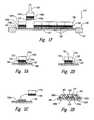
- FIGS. 1A-1Fare partially schematic illustrations of an apparatus and process for reducing the thickness of microelectronic dies in accordance with an embodiment of the invention.
- a microelectronic substrate 120can be attached to a first processing support member 130 with a first attachment device 150 to form a microelectronic assembly 110 .
- the microelectronic substrate 120can include a semiconductor wafer and in other embodiments, the microelectronic substrate 120 can include other substrate structures.
- the microelectronic substrate 120can have a first surface 121 , a second surface 122 facing opposite from the first surface 121 , and an initial thickness T 1 between the first surface 121 and the second surface 122 .
- the microelectronic substrate 120can include a plurality of circuit devices or elements 123 (shown schematically in the Figures) positioned at least proximate to the first surface 121 .
- the circuit elements 123can include lines, vias, terminals, transistors, data storage elements, or other conductor or semiconductor components.
- the circuit elements 123can be formed in and/or on the microelectronic substrate 120 using existing techniques, including but not limited to selective deposition, etching, damascene and dual damascene techniques.
- the microelectronic substrate 120can be positioned relative to the first processing support member 130 such that the first surface 121 faces toward the first processing support member 130 .
- the first attachment device 150can be positioned between the first processing support member 130 and the first surface 121 of the microelectronic substrate 120 to releasably attach the microelectronic substrate 120 to the first processing support member 130 .
- the first attachment device 150can include an adhesive layer 151 disposed on the first processing support member 130 .
- the adhesive layer 151can include a generally planar carrier 152 , a first adhesive 153 facing toward the first processing support member 130 , and a second adhesive 154 facing toward the microelectronic substrate 120 .
- the first adhesive 153can connect the first attachment device 150 to the first processing support member 130
- the second adhesive 154can releasably connect the first attachment device 150 to the microelectronic substrate 120 .
- the first attachment device 150can include other arrangements for coupling the microelectronic substrate 120 to the first processing support member 130 .
- the first processing support member 130can be sized and shaped to receive the microelectronic substrate 120 and provide support to the microelectronic substrate 120 during subsequent processing steps.
- the first processing support member 130can be generally rigid and can have a planform shape at least approximately identical to that of the microelectronic substrate 120 .
- the first processing support member 130can be slightly larger than the microelectronic substrate 120 (as indicated in dashed lines in FIG. 1A) to avoid the need for precisely aligning the microelectronic substrate 120 with the first processing support member 130 when attaching the two together.
- characteristics of the first processing support member 130can be tailored to and/or selected based on the characteristics of the second adhesive 154 .
- the second adhesive 154can have properties that change when the second adhesive 154 is exposed to one or more selected energies.
- the second adhesive 154can have a first level of adhesiveness (e.g., tackiness or stickiness) prior to being exposed to a selected energy, and can have a second, lower level of adhesiveness after being exposed to the selected energy.
- the second adhesive 154can have a lower level of adhesiveness when exposed to ultraviolet radiation.
- the second adhesivecan include an acrylic material.
- the second adhesive 154can include Lintec D175 available from Lintec Corp. of Tokyo, Japan or UC-353ET-110 or UC-337ET-90, both available from Furukawa Electric of Tokyo, Japan.
- the adhesive properties of the second adhesive 154can change upon exposure to other energies, for example, heat energy. Further aspects of an embodiment for which the second adhesive 154 changes adhesive qualities upon exposure to heat energy are described below with reference to FIGS. 2B-2C.
- the first processing support member 130can be at least partially transmissive to the energy that reduces the adhesiveness of the second adhesive 154 .
- the first processing support member 130can include quartz, glass, or another material that is at least partially transmissive to ultraviolet radiation.
- the second adhesive 154 and the first processing support member 130can have other characteristics that allow the first processing support member 130 to (a) support the microelectronic substrate 120 and (b) transmit a sufficient quantity of the type or types of energy that alter characteristics of the second adhesive 154 .
- the additional processingcan include removing material from the second surface 122 of the microelectronic substrate 120 to reduce its thickness. Accordingly, the microelectronic substrate 120 can have a reduced thickness T 2 after processing, as shown in FIG. 1 B.
- the materialcan be removed from the second surface 122 by grinding and/or etching. In other embodiments, the material can be removed from the second surface 122 in accordance with other existing processes.
- the first processing support member 130can provide sufficient support to the microelectronic substrate. 120 to prevent it from breaking and/or excessively warping.
- the thickness of the microelectronic assembly 110 after it has been thinnedmay be slightly greater than that of a conventional microelectronic substrate, but otherwise the overall size and shape of the microelectronic assembly 110 can be generally the same as the size and shape of conventional microelectronic substrates 120 . Accordingly, the equipment and steps used to process the microelectronic substrate 120 with the first processing support member 130 attached can be similar or identical to the equipment and steps used to process existing microelectronic substrates 120 .
- the microelectronic substrate 120 and the first processing support member 130can next be inverted and attached as a unit to a second processing support member 140 .
- the second processing support member 140can include an existing dicing support having a frame 141 carrying a replaceable film 142 .
- the film 142can support a second attachment device 160 which, in one embodiment, includes a third adhesive 161 that releasably adheres to the second surface 122 of the microelectronic substrate 120 .
- the second processing support member 140can support the second surface 122 of the microelectronic substrate 120 , while the first processing support member 130 continues to provide support for the first surface 121 .
- the microelectronic substrate 120can be diced, singulated, or otherwise separated to produce a plurality of microelectronic dies 124 , including a first die 124 a and a second die 124 b , separated by incisions 111 .
- a mechanical cutting wheelcan be used to form the incisions 111
- other techniques, including laser cutting techniquescan be used to create the division between the first die 124 a and the second die 124 b .
- the incision 111can extend through the first processing support member 130 , through the first attachment device 150 , through the microelectronic substrate 120 , and into the second processing support member 140 .
- the second attachment device 160 located between the second support member 140 and the microelectronic substrate 120is released.
- the second attachment device 160can include a radiation-sensitive third adhesive 161 , which has a reduced adhesiveness when exposed to a first radiation R 1 represented schematically by arrows in FIG. 1 E.
- the third adhesive 161can have properties generally similar to those of the second adhesive 154 , while in other embodiments, the third adhesive 161 can have different characteristics.
- the film 142 on which the third adhesive 161 is disposedcan be at least partially transmissive to the first radiation R 1 . As the third adhesive 161 is irradiated through the film 142 , its adhesiveness lessens, allowing the microelectronic dies 124 to be removed from the second support member 140 , as described below with reference to FIG. 1 F.
- a conventional pick-and-place apparatus 170can be used to remove the first die 124 a , a first portion 155 a of the first attachment device 150 , and a first portion 131 a of the first processing support member 130 (as a unit) from the remainder of the microelectronic assembly 110 .
- the third adhesive 161itself remains attached to the film 142 so as not to be removed with the first die 124 a .
- the third adhesive 161can be removed along with the first die 124 a and can later be removed from the first die 124 a in a separate step.
- the first die 124 a , the first portion 155 a of the first attachment device 150 , and the first portion 131 a of the first processing support member 130can be removed while the second die 124 b , a second portion 155 b of the first attachment device 150 , and a second portion 131 b of the first processing support member 130 remain proximate to the second processing support member 140 .
- the foregoing removal processcan then be repeated for the second die 124 b and other dies 124 .
- the first die 124 aAfter the first die 124 a has been separated from the microelectronic substrate 120 , it can be packaged. One process for packaging the first die 124 a is described below with reference to FIGS. 2A-2D.
- the first die 124 a(together with the first portions 155 a and 131 a ) can be attached, as a unit, to a die attach member 180 .
- the die attach member 180can include a printed circuit board, and in other embodiments, the die attach member 180 can include other suitable substrates.
- the first die 124 acan be attached to the die attach member 180 with a die attach adhesive 181 disposed at an interface between these two components.
- the first portion 155 a of first attachment device 150can be released to allow the first portion 131 a of the first processing support member 130 to be removed from the first die 124 a .
- a second radiation R 2can be directed through the first portion 131 a to reduce the adhesiveness of the second adhesive 154 .
- the second radiation R 2can include ultraviolet radiation, for example, having a wavelength in the range of from about 220 nm to about 365 nm.
- the second radiation R 2can have a different wavelength.
- another energyfor example, heat energy
- the first portion 131 a of the first processing support member 130 and the first portion 155 a of the first attachment device 150can be removed as a unit from the first die 124 a , as shown in FIG. 2 C.
- the energy used to reduce the strength of the bond between the first die 124 a and the first attachment device 150can simultaneously increase the strength of the bond between the die attach adhesive 181 and the first die 124 a .
- the second adhesive 154can be selected to decrease in adhesiveness when exposed to heat at a selected temperature, and the die attach adhesive 181 can be selected to increase in adhesiveness at the same temperature.
- the second adhesive 154can be selected to include Revalpha #3195MS heat release tape (which decreases its bond strength at a temperature of from about 90° C. to about 150° C.
- the die attach adhesive 181can be selected to include QMI536 (which increases its bond strength over the same temperature range and which is available from Dexter/Loctite of Rocky Hill, Conn.).
- the second adhesive 154 and the die attach adhesive 181can include other substances having adhesive characteristics that behave in opposite manners when exposed to the same energy.
- the first die 124 acan be electrically coupled to the die attach member 180 .
- the first die 124 acan include die bond pads 125 which can be electrically coupled to first attach member bond pads 182 a .
- the attachment between these two componentscan be made with wire bonds 183 , and in other embodiments, other conductive links (including solder balls), can be used to connect the die bond pads 125 with the corresponding first attach member bond pads 182 a .
- the die attach member 180can further include second attach member bond pads 182 b which are electrically coupled to the first attach member bond pads 182 a via circuitry internal to the die attach member 180 .
- the second attach member bond pads 182 bcan be electrically coupled to other microelectronic devices via solder balls or other conductive structures to provide electrical signals to and from the first die 124 a .
- An encapsulant 183can optionally be disposed over the wire bonds 183 and the first die 124 a to protect these components.
- One feature of an embodiment of the apparatus and process described above with reference to FIGS. 1A-2Dis that the first processing support member 130 can remain attached to the microelectronic substrate 120 as the microelectronic substrate 120 is thinned and attached to the second processing support member 140 .
- An advantage of this featureis that the microelectronic substrate 120 can be less likely to be damaged or broken as it is transferred from a grinder or other thickness-reducing tool to the second processing support member 140 .
- first portion 131 a of the first processing support member 130can remain attached to the first die 124 a as the first die 124 a is moved from the second processing support member 140 to the die attach member 180 .
- the first portion 131 a of the first processing support member 130is removed.
- An advantage of this arrangementis that the first die 124 a is less likely to be damaged as it is moved from the second processing support member 140 to the die attach member 180 because the first portion 131 a of the first processing support member 130 provides support and protection.
- the first portion 131 acan shield the first surface 121 and the proximate circuit elements 123 from incidental contact with surrounding tools, machinery and/or other components.
- the first portion 131 acan also provide a generally rigid support structure that reduces the likelihood for the first die 124 a to bend as it is moved.
- the second adhesive 154 and/or the third adhesive 161can be made less adhesive by exposure to energies other than ultraviolet radiation.
- energiescan include electromagnetic radiation having frequencies other than ultraviolet frequencies, or other types of energy, such as heat energy. Accordingly, the invention is not limited except as by the appended claims.
Landscapes
- Engineering & Computer Science (AREA)
- Computer Hardware Design (AREA)
- Microelectronics & Electronic Packaging (AREA)
- Power Engineering (AREA)
- Physics & Mathematics (AREA)
- Condensed Matter Physics & Semiconductors (AREA)
- General Physics & Mathematics (AREA)
- Manufacturing & Machinery (AREA)
- Container, Conveyance, Adherence, Positioning, Of Wafer (AREA)
Abstract
Description
Claims (49)
Priority Applications (2)
| Application Number | Priority Date | Filing Date | Title |
|---|---|---|---|
| US10/348,635US6762074B1 (en) | 2003-01-21 | 2003-01-21 | Method and apparatus for forming thin microelectronic dies |
| US10/835,369US6882036B2 (en) | 2003-01-21 | 2004-04-29 | Apparatuses for forming thin microelectronic dies |
Applications Claiming Priority (1)
| Application Number | Priority Date | Filing Date | Title |
|---|---|---|---|
| US10/348,635US6762074B1 (en) | 2003-01-21 | 2003-01-21 | Method and apparatus for forming thin microelectronic dies |
Related Child Applications (1)
| Application Number | Title | Priority Date | Filing Date |
|---|---|---|---|
| US10/835,369DivisionUS6882036B2 (en) | 2003-01-21 | 2004-04-29 | Apparatuses for forming thin microelectronic dies |
Publications (1)
| Publication Number | Publication Date |
|---|---|
| US6762074B1true US6762074B1 (en) | 2004-07-13 |
Family
ID=32681615
Family Applications (2)
| Application Number | Title | Priority Date | Filing Date |
|---|---|---|---|
| US10/348,635Expired - LifetimeUS6762074B1 (en) | 2003-01-21 | 2003-01-21 | Method and apparatus for forming thin microelectronic dies |
| US10/835,369Expired - Fee RelatedUS6882036B2 (en) | 2003-01-21 | 2004-04-29 | Apparatuses for forming thin microelectronic dies |
Family Applications After (1)
| Application Number | Title | Priority Date | Filing Date |
|---|---|---|---|
| US10/835,369Expired - Fee RelatedUS6882036B2 (en) | 2003-01-21 | 2004-04-29 | Apparatuses for forming thin microelectronic dies |
Country Status (1)
| Country | Link |
|---|---|
| US (2) | US6762074B1 (en) |
Cited By (32)
| Publication number | Priority date | Publication date | Assignee | Title |
|---|---|---|---|---|
| US20060258051A1 (en)* | 2005-05-10 | 2006-11-16 | Texas Instruments Incorporated | Method and system for solder die attach |
| US20070031989A1 (en)* | 2003-02-27 | 2007-02-08 | Roy Knechtel | Separating semiconductor wafers having exposed micromechanical structures into individual chips |
| US20080036084A1 (en)* | 2006-01-30 | 2008-02-14 | International Business Machines Corporation | Laser release process for very thin Si-carrier build |
| US20090251879A1 (en)* | 2008-04-04 | 2009-10-08 | Thompson Jeffrey C | Die thinning processes and structures |
| US20090250823A1 (en)* | 2008-04-04 | 2009-10-08 | Racz Livia M | Electronic Modules and Methods for Forming the Same |
| US20090250249A1 (en)* | 2008-04-04 | 2009-10-08 | Racz Livia M | Interposers, electronic modules, and methods for forming the same |
| US20110217814A1 (en)* | 2008-10-23 | 2011-09-08 | Freescale Semiconductor, Inc. | Method for singulating electronic components from a substrate |
| JP2011228362A (en)* | 2010-04-15 | 2011-11-10 | Disco Abrasive Syst Ltd | Manufacturing method of semiconductor device |
| JP2011228474A (en)* | 2010-04-20 | 2011-11-10 | Disco Abrasive Syst Ltd | Manufacturing method of semiconductor device |
| US20110290413A1 (en)* | 2010-05-27 | 2011-12-01 | International Business Machines Corporation | Laser Ablation of Adhesive for Integrated Circuit Fabrication |
| US8080121B2 (en) | 2006-07-28 | 2011-12-20 | Tokyo Ohka Kogyo Co., Ltd. | Method of bonding, thinning, and releasing wafer |
| US20120156858A1 (en)* | 2010-12-17 | 2012-06-21 | Disco Corporation | Optical device wafer processing method |
| WO2013116167A1 (en)* | 2012-02-02 | 2013-08-08 | Harris Corporation | Method for making a redistributed wafer using transferable redistribution layers |
| WO2013116168A1 (en)* | 2012-02-02 | 2013-08-08 | Harris Corporation | Method for making a redistributed electronic device using a transferrable redistribution layer |
| US9340443B2 (en) | 2012-12-13 | 2016-05-17 | Corning Incorporated | Bulk annealing of glass sheets |
| US20160336304A1 (en)* | 2015-05-15 | 2016-11-17 | Au Optronics Corporation | Method for transferring micro devices and method for manufacturing display panel |
| US9889635B2 (en) | 2012-12-13 | 2018-02-13 | Corning Incorporated | Facilitated processing for controlling bonding between sheet and carrier |
| US10014177B2 (en) | 2012-12-13 | 2018-07-03 | Corning Incorporated | Methods for processing electronic devices |
| US10046542B2 (en) | 2014-01-27 | 2018-08-14 | Corning Incorporated | Articles and methods for controlled bonding of thin sheets with carriers |
| US10086584B2 (en) | 2012-12-13 | 2018-10-02 | Corning Incorporated | Glass articles and methods for controlled bonding of glass sheets with carriers |
| US10510576B2 (en) | 2013-10-14 | 2019-12-17 | Corning Incorporated | Carrier-bonding methods and articles for semiconductor and interposer processing |
| US10543662B2 (en) | 2012-02-08 | 2020-01-28 | Corning Incorporated | Device modified substrate article and methods for making |
| US20210183682A1 (en)* | 2019-12-16 | 2021-06-17 | Micron Technology, Inc. | Methods and apparatus for protection of dielectric films during microelectronic component processing |
| US11097509B2 (en) | 2016-08-30 | 2021-08-24 | Corning Incorporated | Siloxane plasma polymers for sheet bonding |
| US11167532B2 (en) | 2015-05-19 | 2021-11-09 | Corning Incorporated | Articles and methods for bonding sheets with carriers |
| US11192340B2 (en) | 2014-04-09 | 2021-12-07 | Corning Incorporated | Device modified substrate article and methods for making |
| US11331692B2 (en) | 2017-12-15 | 2022-05-17 | Corning Incorporated | Methods for treating a substrate and method for making articles comprising bonded sheets |
| US11535553B2 (en) | 2016-08-31 | 2022-12-27 | Corning Incorporated | Articles of controllably bonded sheets and methods for making same |
| US11729915B1 (en)* | 2022-03-22 | 2023-08-15 | Tactotek Oy | Method for manufacturing a number of electrical nodes, electrical node module, electrical node, and multilayer structure |
| US20230420300A1 (en)* | 2019-12-13 | 2023-12-28 | Micron Technology, Inc. | Thin die release for semiconductor device assembly |
| US11905201B2 (en) | 2015-06-26 | 2024-02-20 | Corning Incorporated | Methods and articles including a sheet and a carrier |
| US11999135B2 (en) | 2017-08-18 | 2024-06-04 | Corning Incorporated | Temporary bonding using polycationic polymers |
Families Citing this family (6)
| Publication number | Priority date | Publication date | Assignee | Title |
|---|---|---|---|---|
| US20050182159A1 (en)* | 2003-03-20 | 2005-08-18 | Jrs Corporation | Diene rubber-inorganic compound composite and process for producing the same |
| US8628311B2 (en)* | 2007-09-11 | 2014-01-14 | Boston Scientific Scimed, Inc. | Thermal ablation system with dispensable therapeutic agent |
| JP5382029B2 (en)* | 2011-02-22 | 2014-01-08 | オムロン株式会社 | Microphone manufacturing method |
| JP6029348B2 (en)* | 2012-06-26 | 2016-11-24 | 株式会社ディスコ | Wafer processing method |
| JP6029347B2 (en)* | 2012-06-26 | 2016-11-24 | 株式会社ディスコ | Wafer processing method |
| US11784092B2 (en)* | 2020-02-27 | 2023-10-10 | Micron Technology, Inc. | Disposing protective cover film and underfill layer over singulated integrated circuit dice for protection during integrated circuit processing |
Citations (14)
| Publication number | Priority date | Publication date | Assignee | Title |
|---|---|---|---|---|
| US5851845A (en) | 1995-12-18 | 1998-12-22 | Micron Technology, Inc. | Process for packaging a semiconductor die using dicing and testing |
| US5933713A (en) | 1998-04-06 | 1999-08-03 | Micron Technology, Inc. | Method of forming overmolded chip scale package and resulting product |
| US5946553A (en) | 1991-06-04 | 1999-08-31 | Micron Technology, Inc. | Process for manufacturing a semiconductor package with bi-substrate die |
| US6004867A (en) | 1996-12-16 | 1999-12-21 | Samsung Electronics Co., Ltd. | Chip-size packages assembled using mass production techniques at the wafer-level |
| US6008070A (en) | 1998-05-21 | 1999-12-28 | Micron Technology, Inc. | Wafer level fabrication and assembly of chip scale packages |
| US6072236A (en) | 1996-03-07 | 2000-06-06 | Micron Technology, Inc. | Micromachined chip scale package |
| US6175162B1 (en) | 1998-01-14 | 2001-01-16 | National Semiconductor Corporation | Semiconductor wafer having a bottom surface protective coating |
| US6184465B1 (en) | 1998-11-12 | 2001-02-06 | Micron Technology, Inc. | Semiconductor package |
| US6187615B1 (en) | 1998-08-28 | 2001-02-13 | Samsung Electronics Co., Ltd. | Chip scale packages and methods for manufacturing the chip scale packages at wafer level |
| US6228687B1 (en) | 1999-06-28 | 2001-05-08 | Micron Technology, Inc. | Wafer-level package and methods of fabricating |
| US6235552B1 (en) | 1999-07-09 | 2001-05-22 | Samsung Electronics Co., Ltd. | Chip scale package and method for manufacturing the same using a redistribution substrate |
| US6326698B1 (en) | 2000-06-08 | 2001-12-04 | Micron Technology, Inc. | Semiconductor devices having protective layers thereon through which contact pads are exposed and stereolithographic methods of fabricating such semiconductor devices |
| US6407381B1 (en) | 2000-07-05 | 2002-06-18 | Amkor Technology, Inc. | Wafer scale image sensor package |
| US6503780B1 (en) | 2000-07-05 | 2003-01-07 | Amkor Technology, Inc. | Wafer scale image sensor package fabrication method |
Family Cites Families (2)
| Publication number | Priority date | Publication date | Assignee | Title |
|---|---|---|---|---|
| US6759273B2 (en)* | 2000-12-05 | 2004-07-06 | Analog Devices, Inc. | Method and device for protecting micro electromechanical systems structures during dicing of a wafer |
| JP3608615B2 (en)* | 2001-04-19 | 2005-01-12 | ソニー株式会社 | Device transfer method, device array method using the same, and image display device manufacturing method |
- 2003
- 2003-01-21USUS10/348,635patent/US6762074B1/ennot_activeExpired - Lifetime
- 2004
- 2004-04-29USUS10/835,369patent/US6882036B2/ennot_activeExpired - Fee Related
Patent Citations (17)
| Publication number | Priority date | Publication date | Assignee | Title |
|---|---|---|---|---|
| US5946553A (en) | 1991-06-04 | 1999-08-31 | Micron Technology, Inc. | Process for manufacturing a semiconductor package with bi-substrate die |
| US6020624A (en) | 1991-06-04 | 2000-02-01 | Micron Technology, Inc. | Semiconductor package with bi-substrate die |
| US5851845A (en) | 1995-12-18 | 1998-12-22 | Micron Technology, Inc. | Process for packaging a semiconductor die using dicing and testing |
| US6072236A (en) | 1996-03-07 | 2000-06-06 | Micron Technology, Inc. | Micromachined chip scale package |
| US6124634A (en) | 1996-03-07 | 2000-09-26 | Micron Technology, Inc. | Micromachined chip scale package |
| US6004867A (en) | 1996-12-16 | 1999-12-21 | Samsung Electronics Co., Ltd. | Chip-size packages assembled using mass production techniques at the wafer-level |
| US6175162B1 (en) | 1998-01-14 | 2001-01-16 | National Semiconductor Corporation | Semiconductor wafer having a bottom surface protective coating |
| US5933713A (en) | 1998-04-06 | 1999-08-03 | Micron Technology, Inc. | Method of forming overmolded chip scale package and resulting product |
| US6008070A (en) | 1998-05-21 | 1999-12-28 | Micron Technology, Inc. | Wafer level fabrication and assembly of chip scale packages |
| US6326697B1 (en) | 1998-05-21 | 2001-12-04 | Micron Technology, Inc. | Hermetically sealed chip scale packages formed by wafer level fabrication and assembly |
| US6187615B1 (en) | 1998-08-28 | 2001-02-13 | Samsung Electronics Co., Ltd. | Chip scale packages and methods for manufacturing the chip scale packages at wafer level |
| US6184465B1 (en) | 1998-11-12 | 2001-02-06 | Micron Technology, Inc. | Semiconductor package |
| US6228687B1 (en) | 1999-06-28 | 2001-05-08 | Micron Technology, Inc. | Wafer-level package and methods of fabricating |
| US6235552B1 (en) | 1999-07-09 | 2001-05-22 | Samsung Electronics Co., Ltd. | Chip scale package and method for manufacturing the same using a redistribution substrate |
| US6326698B1 (en) | 2000-06-08 | 2001-12-04 | Micron Technology, Inc. | Semiconductor devices having protective layers thereon through which contact pads are exposed and stereolithographic methods of fabricating such semiconductor devices |
| US6407381B1 (en) | 2000-07-05 | 2002-06-18 | Amkor Technology, Inc. | Wafer scale image sensor package |
| US6503780B1 (en) | 2000-07-05 | 2003-01-07 | Amkor Technology, Inc. | Wafer scale image sensor package fabrication method |
Cited By (54)
| Publication number | Priority date | Publication date | Assignee | Title |
|---|---|---|---|---|
| US20070031989A1 (en)* | 2003-02-27 | 2007-02-08 | Roy Knechtel | Separating semiconductor wafers having exposed micromechanical structures into individual chips |
| US20060258051A1 (en)* | 2005-05-10 | 2006-11-16 | Texas Instruments Incorporated | Method and system for solder die attach |
| US20080036084A1 (en)* | 2006-01-30 | 2008-02-14 | International Business Machines Corporation | Laser release process for very thin Si-carrier build |
| US20090032920A1 (en)* | 2006-01-30 | 2009-02-05 | International Business Machines Corporation | Laser release process for very thin si-carrier build |
| US8187923B2 (en) | 2006-01-30 | 2012-05-29 | International Business Machines Corporation | Laser release process for very thin Si-carrier build |
| US8080121B2 (en) | 2006-07-28 | 2011-12-20 | Tokyo Ohka Kogyo Co., Ltd. | Method of bonding, thinning, and releasing wafer |
| US20090250249A1 (en)* | 2008-04-04 | 2009-10-08 | Racz Livia M | Interposers, electronic modules, and methods for forming the same |
| US7960247B2 (en) | 2008-04-04 | 2011-06-14 | The Charles Stark Draper Laboratory, Inc. | Die thinning processes and structures |
| US20090250823A1 (en)* | 2008-04-04 | 2009-10-08 | Racz Livia M | Electronic Modules and Methods for Forming the Same |
| US8017451B2 (en) | 2008-04-04 | 2011-09-13 | The Charles Stark Draper Laboratory, Inc. | Electronic modules and methods for forming the same |
| US8273603B2 (en) | 2008-04-04 | 2012-09-25 | The Charles Stark Draper Laboratory, Inc. | Interposers, electronic modules, and methods for forming the same |
| US8535984B2 (en) | 2008-04-04 | 2013-09-17 | The Charles Stark Draper Laboratory, Inc. | Electronic modules and methods for forming the same |
| US20090251879A1 (en)* | 2008-04-04 | 2009-10-08 | Thompson Jeffrey C | Die thinning processes and structures |
| US9142434B2 (en)* | 2008-10-23 | 2015-09-22 | Freescale Semiconductor, Inc. | Method for singulating electronic components from a substrate |
| US20110217814A1 (en)* | 2008-10-23 | 2011-09-08 | Freescale Semiconductor, Inc. | Method for singulating electronic components from a substrate |
| JP2011228362A (en)* | 2010-04-15 | 2011-11-10 | Disco Abrasive Syst Ltd | Manufacturing method of semiconductor device |
| JP2011228474A (en)* | 2010-04-20 | 2011-11-10 | Disco Abrasive Syst Ltd | Manufacturing method of semiconductor device |
| US8389386B2 (en)* | 2010-04-20 | 2013-03-05 | Disco Corporation | Stacked wafer manufacturing method |
| US20110290413A1 (en)* | 2010-05-27 | 2011-12-01 | International Business Machines Corporation | Laser Ablation of Adhesive for Integrated Circuit Fabrication |
| US8679280B2 (en)* | 2010-05-27 | 2014-03-25 | International Business Machines Corporation | Laser ablation of adhesive for integrated circuit fabrication |
| US9048349B2 (en)* | 2010-12-17 | 2015-06-02 | Disco Corporation | Optical device wafer processing method |
| US20120156858A1 (en)* | 2010-12-17 | 2012-06-21 | Disco Corporation | Optical device wafer processing method |
| WO2013116168A1 (en)* | 2012-02-02 | 2013-08-08 | Harris Corporation | Method for making a redistributed electronic device using a transferrable redistribution layer |
| CN104094398A (en)* | 2012-02-02 | 2014-10-08 | 哈里公司 | Method for making a redistributed wafer using transferable redistribution layers |
| KR101495014B1 (en)* | 2012-02-02 | 2015-02-23 | 해리스 코포레이션 | Method for making a redistributed electronic device using a transferrable redistribution layer |
| WO2013116167A1 (en)* | 2012-02-02 | 2013-08-08 | Harris Corporation | Method for making a redistributed wafer using transferable redistribution layers |
| US8685761B2 (en) | 2012-02-02 | 2014-04-01 | Harris Corporation | Method for making a redistributed electronic device using a transferrable redistribution layer |
| US8772058B2 (en) | 2012-02-02 | 2014-07-08 | Harris Corporation | Method for making a redistributed wafer using transferrable redistribution layers |
| US10543662B2 (en) | 2012-02-08 | 2020-01-28 | Corning Incorporated | Device modified substrate article and methods for making |
| US9889635B2 (en) | 2012-12-13 | 2018-02-13 | Corning Incorporated | Facilitated processing for controlling bonding between sheet and carrier |
| US10014177B2 (en) | 2012-12-13 | 2018-07-03 | Corning Incorporated | Methods for processing electronic devices |
| US10086584B2 (en) | 2012-12-13 | 2018-10-02 | Corning Incorporated | Glass articles and methods for controlled bonding of glass sheets with carriers |
| US10538452B2 (en) | 2012-12-13 | 2020-01-21 | Corning Incorporated | Bulk annealing of glass sheets |
| US9340443B2 (en) | 2012-12-13 | 2016-05-17 | Corning Incorporated | Bulk annealing of glass sheets |
| US10510576B2 (en) | 2013-10-14 | 2019-12-17 | Corning Incorporated | Carrier-bonding methods and articles for semiconductor and interposer processing |
| US11123954B2 (en) | 2014-01-27 | 2021-09-21 | Corning Incorporated | Articles and methods for controlled bonding of thin sheets with carriers |
| US10046542B2 (en) | 2014-01-27 | 2018-08-14 | Corning Incorporated | Articles and methods for controlled bonding of thin sheets with carriers |
| US11192340B2 (en) | 2014-04-09 | 2021-12-07 | Corning Incorporated | Device modified substrate article and methods for making |
| US20160336304A1 (en)* | 2015-05-15 | 2016-11-17 | Au Optronics Corporation | Method for transferring micro devices and method for manufacturing display panel |
| US9698160B2 (en)* | 2015-05-15 | 2017-07-04 | Au Optronics Corporation | Method for transferring micro devices and method for manufacturing display panel |
| US11167532B2 (en) | 2015-05-19 | 2021-11-09 | Corning Incorporated | Articles and methods for bonding sheets with carriers |
| US11660841B2 (en) | 2015-05-19 | 2023-05-30 | Corning Incorporated | Articles and methods for bonding sheets with carriers |
| US11905201B2 (en) | 2015-06-26 | 2024-02-20 | Corning Incorporated | Methods and articles including a sheet and a carrier |
| US11097509B2 (en) | 2016-08-30 | 2021-08-24 | Corning Incorporated | Siloxane plasma polymers for sheet bonding |
| US12122138B2 (en) | 2016-08-30 | 2024-10-22 | Corning Incorporated | Siloxane plasma polymers for sheet bonding |
| US11535553B2 (en) | 2016-08-31 | 2022-12-27 | Corning Incorporated | Articles of controllably bonded sheets and methods for making same |
| US12344548B2 (en) | 2016-08-31 | 2025-07-01 | Corning Incorporated | Methods for making controllably bonded sheets |
| US11999135B2 (en) | 2017-08-18 | 2024-06-04 | Corning Incorporated | Temporary bonding using polycationic polymers |
| US11331692B2 (en) | 2017-12-15 | 2022-05-17 | Corning Incorporated | Methods for treating a substrate and method for making articles comprising bonded sheets |
| US20230420300A1 (en)* | 2019-12-13 | 2023-12-28 | Micron Technology, Inc. | Thin die release for semiconductor device assembly |
| US11289360B2 (en)* | 2019-12-16 | 2022-03-29 | Micron Technology, Inc. | Methods and apparatus for protection of dielectric films during microelectronic component processing |
| US20210183682A1 (en)* | 2019-12-16 | 2021-06-17 | Micron Technology, Inc. | Methods and apparatus for protection of dielectric films during microelectronic component processing |
| US11729915B1 (en)* | 2022-03-22 | 2023-08-15 | Tactotek Oy | Method for manufacturing a number of electrical nodes, electrical node module, electrical node, and multilayer structure |
| US12052829B2 (en) | 2022-03-22 | 2024-07-30 | Tactotek Oy | Method for manufacturing a number of electrical nodes, electrical node module, electrical node, and multilayer structure |
Also Published As
| Publication number | Publication date |
|---|---|
| US20040203188A1 (en) | 2004-10-14 |
| US6882036B2 (en) | 2005-04-19 |
Similar Documents
| Publication | Publication Date | Title |
|---|---|---|
| US6762074B1 (en) | Method and apparatus for forming thin microelectronic dies | |
| CN110546754B (en) | Grain processing | |
| TWI284960B (en) | Manufacturing method of semiconductor device | |
| US6750082B2 (en) | Method of assembling a package with an exposed die backside with and without a heatsink for flip-chip | |
| KR101561359B1 (en) | Stacked body and method for detaching stacked body | |
| US10354977B2 (en) | Semiconductor device and manufacturing method thereof | |
| US20070048902A1 (en) | Microfeature workpieces, carriers, and associated methods | |
| JP2001313350A (en) | Chip-shaped electronic component and its manufacturing method, and pseudo-wafer used for manufacture of chip- shaped electronic component and its manufacturing method | |
| KR20140044879A (en) | Dicing before grinding after coating | |
| US9281182B2 (en) | Pre-cut wafer applied underfill film | |
| CN101958255B (en) | Ultra-thin wafer processing method and thin wafer processing product | |
| US7846776B2 (en) | Methods for releasably attaching sacrificial support members to microfeature workpieces and microfeature devices formed using such methods | |
| US7105424B2 (en) | Method for preparing arylphosphonite antioxidant | |
| US9362105B2 (en) | Pre-cut wafer applied underfill film on dicing tape | |
| US10490531B2 (en) | Manufacturing method of semiconductor device and semiconductor device | |
| JP2001135598A (en) | Wafer dicing method, semiconductor device and its manufacturing method, circuit board, and electronic equipment | |
| JPH1174230A (en) | Method for manufacturing thin film semiconductor device | |
| KR102798785B1 (en) | Method of manufacturing semiconductor device | |
| US9462694B2 (en) | Spacer layer for embedding semiconductor die | |
| US8476109B2 (en) | Semiconductor workpiece carriers and methods for processing semiconductor workpieces | |
| JP2006140303A (en) | Method for manufacturing semiconductor apparatus | |
| US20070114672A1 (en) | Semiconductor device and method of manufacturing the same | |
| KR20080114036A (en) | Individualization method of semiconductor chip | |
| WO2012135243A1 (en) | Pre-grooving for wafer applied underfill film | |
| JP2004158776A (en) | Method for manufacturing semiconductor device |
Legal Events
| Date | Code | Title | Description |
|---|---|---|---|
| AS | Assignment | Owner name:MICRON TECHNOLOGY, INC., IDAHO Free format text:ASSIGNMENT OF ASSIGNORS INTEREST;ASSIGNORS:DRANEY, NATHAN R.;CONNELL, MICHAEL E.;REEL/FRAME:013695/0404 Effective date:20030110 | |
| FEPP | Fee payment procedure | Free format text:PAYOR NUMBER ASSIGNED (ORIGINAL EVENT CODE: ASPN); ENTITY STATUS OF PATENT OWNER: LARGE ENTITY | |
| STCF | Information on status: patent grant | Free format text:PATENTED CASE | |
| FPAY | Fee payment | Year of fee payment:4 | |
| FPAY | Fee payment | Year of fee payment:8 | |
| FPAY | Fee payment | Year of fee payment:12 | |
| AS | Assignment | Owner name:U.S. BANK NATIONAL ASSOCIATION, AS COLLATERAL AGENT, CALIFORNIA Free format text:SECURITY INTEREST;ASSIGNOR:MICRON TECHNOLOGY, INC.;REEL/FRAME:038669/0001 Effective date:20160426 Owner name:U.S. BANK NATIONAL ASSOCIATION, AS COLLATERAL AGEN Free format text:SECURITY INTEREST;ASSIGNOR:MICRON TECHNOLOGY, INC.;REEL/FRAME:038669/0001 Effective date:20160426 | |
| AS | Assignment | Owner name:MORGAN STANLEY SENIOR FUNDING, INC., AS COLLATERAL AGENT, MARYLAND Free format text:PATENT SECURITY AGREEMENT;ASSIGNOR:MICRON TECHNOLOGY, INC.;REEL/FRAME:038954/0001 Effective date:20160426 Owner name:MORGAN STANLEY SENIOR FUNDING, INC., AS COLLATERAL Free format text:PATENT SECURITY AGREEMENT;ASSIGNOR:MICRON TECHNOLOGY, INC.;REEL/FRAME:038954/0001 Effective date:20160426 | |
| AS | Assignment | Owner name:U.S. BANK NATIONAL ASSOCIATION, AS COLLATERAL AGENT, CALIFORNIA Free format text:CORRECTIVE ASSIGNMENT TO CORRECT THE REPLACE ERRONEOUSLY FILED PATENT #7358718 WITH THE CORRECT PATENT #7358178 PREVIOUSLY RECORDED ON REEL 038669 FRAME 0001. ASSIGNOR(S) HEREBY CONFIRMS THE SECURITY INTEREST;ASSIGNOR:MICRON TECHNOLOGY, INC.;REEL/FRAME:043079/0001 Effective date:20160426 Owner name:U.S. BANK NATIONAL ASSOCIATION, AS COLLATERAL AGEN Free format text:CORRECTIVE ASSIGNMENT TO CORRECT THE REPLACE ERRONEOUSLY FILED PATENT #7358718 WITH THE CORRECT PATENT #7358178 PREVIOUSLY RECORDED ON REEL 038669 FRAME 0001. ASSIGNOR(S) HEREBY CONFIRMS THE SECURITY INTEREST;ASSIGNOR:MICRON TECHNOLOGY, INC.;REEL/FRAME:043079/0001 Effective date:20160426 | |
| AS | Assignment | Owner name:JPMORGAN CHASE BANK, N.A., AS COLLATERAL AGENT, ILLINOIS Free format text:SECURITY INTEREST;ASSIGNORS:MICRON TECHNOLOGY, INC.;MICRON SEMICONDUCTOR PRODUCTS, INC.;REEL/FRAME:047540/0001 Effective date:20180703 Owner name:JPMORGAN CHASE BANK, N.A., AS COLLATERAL AGENT, IL Free format text:SECURITY INTEREST;ASSIGNORS:MICRON TECHNOLOGY, INC.;MICRON SEMICONDUCTOR PRODUCTS, INC.;REEL/FRAME:047540/0001 Effective date:20180703 | |
| AS | Assignment | Owner name:MICRON TECHNOLOGY, INC., IDAHO Free format text:RELEASE BY SECURED PARTY;ASSIGNOR:U.S. BANK NATIONAL ASSOCIATION, AS COLLATERAL AGENT;REEL/FRAME:047243/0001 Effective date:20180629 | |
| AS | Assignment | Owner name:MICRON TECHNOLOGY, INC., IDAHO Free format text:RELEASE BY SECURED PARTY;ASSIGNOR:MORGAN STANLEY SENIOR FUNDING, INC., AS COLLATERAL AGENT;REEL/FRAME:050937/0001 Effective date:20190731 | |
| AS | Assignment | Owner name:MICRON TECHNOLOGY, INC., IDAHO Free format text:RELEASE BY SECURED PARTY;ASSIGNOR:JPMORGAN CHASE BANK, N.A., AS COLLATERAL AGENT;REEL/FRAME:051028/0001 Effective date:20190731 Owner name:MICRON SEMICONDUCTOR PRODUCTS, INC., IDAHO Free format text:RELEASE BY SECURED PARTY;ASSIGNOR:JPMORGAN CHASE BANK, N.A., AS COLLATERAL AGENT;REEL/FRAME:051028/0001 Effective date:20190731 |