US6760864B2 - Data processing system with on-chip FIFO for storing debug information and method therefor - Google Patents
Data processing system with on-chip FIFO for storing debug information and method thereforDownload PDFInfo
- Publication number
- US6760864B2 US6760864B2US09/788,815US78881501AUS6760864B2US 6760864 B2US6760864 B2US 6760864B2US 78881501 AUS78881501 AUS 78881501AUS 6760864 B2US6760864 B2US 6760864B2
- Authority
- US
- United States
- Prior art keywords
- processing system
- data
- data processing
- address
- current instruction
- Prior art date
- Legal status (The legal status is an assumption and is not a legal conclusion. Google has not performed a legal analysis and makes no representation as to the accuracy of the status listed.)
- Expired - Lifetime, expires
Links
Images


Classifications
- G—PHYSICS
- G06—COMPUTING OR CALCULATING; COUNTING
- G06F—ELECTRIC DIGITAL DATA PROCESSING
- G06F11/00—Error detection; Error correction; Monitoring
- G06F11/36—Prevention of errors by analysis, debugging or testing of software
- G06F11/362—Debugging of software
- G06F11/3636—Debugging of software by tracing the execution of the program
- G06F11/364—Debugging of software by tracing the execution of the program tracing values on a bus
Definitions
- the present inventionrelates generally to data processing systems, and more particularly, to a data processing system with an on-chip debug FIFO capable of storing change-of-flow addresses, data values, or current instruction addresses.
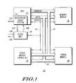
- FIG. 1illustrates, in block diagram form, a data processing system in accordance with the present invention.
- FIG. 2illustrates a debug module of the data processing system of FIG. 1 .
- FIG. 3illustrates, in block diagram form, the background debug system of FIG. 1 .
- the present inventionprovides a debugging module in a data processing system using a first-in, first-out (FIFO) memory to store certain debug related information.
- the debug related informationincludes, for example, change-of-flow addresses, central processing unit (CPU) data values, and current instruction addresses.
- the data processing systemdoes not have dedicated pins for monitoring internal address and data buses.
- the debugging moduleincludes a FIFO for temporarily storing the debug information before providing it to an external system via a serial communication interface.
- the debugging moduleoperates autonomously of the CPU and allows real time program debugging in data processing systems that do not have dedicated pins for monitoring internal address and data buses.
- busis used to refer to a plurality of signals or conductors which may be used to transfer one or more various types of information, such as data, addresses, control, or status.
- assertis used when referring to the rendering of a signal, status bit, or similar apparatus into its logically true state.
- gateor “deassert” is used when referring to the rendering of a signal, status bit, or similar apparatus into its logically false state. If a signal (or status bit, etc.) is active high, the logically true state is a logic level one, and the logically false state is a logic level zero.
- a signal(or status bit, etc.) is active low, the logically true state is a logic level zero, and the logically false state is a logic level one. Also, “high” may be used to refer to a logic level one while “low” may be used to refer to a logic level zero.
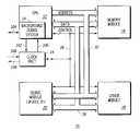
- FIG. 1illustrates, in block diagram form, a data processing system 10 in accordance with one embodiment of the present invention.
- Data processing system 10can be any processing system such as a microcontroller, microprocessor, digital signal processor (DSP), or the like.
- Data processing system 10includes CPU 12 , clock unit 19 , memory module 16 , other module 18 , debug module 20 , internal address bus 22 , internal data bus 24 , and control signals 26 .
- CPU 12includes a background debug system (BDS) 14 .
- BDS 14includes a serial background communication interface 104 .
- Internal data bus 24 , internal address bus 22 , and control signals 26are coupled between CPU 12 and each of the peripheral modules on data processing system 10 .
- Clock unit 19is coupled to CPU 12 via control signals 26 and to BDS 14 via signals 102 and 106 .
- Clock unit 19also includes interface signals 108 and 109 for coupling to an oscillator circuit (not shown).
- CPU 12receives and executes instructions from a software program stored in memory module 16 via data bus 24 .
- CPU 12then directs or uses other resources of the data processing system to perform certain tasks.
- Memory module 16may be any type of memory including, but not limited to, static random access memory, dynamic random access memory, or any type of non-volatile memory, such as for example, flash or EEPROM.
- Other module 18may include one or more additional modules, such as for example, another memory module, an analog-to-digital converter, a timer module, a serial communications module, for example, a CAN module, a general purpose input/output module, or the like.
- Debug module 20is illustrated in greater detail in FIG. 2 and allows for program debugging.
- Clock unit 19is coupled to background debug system 14 via EN_BDM 102 and background debug clock 106 (see FIG. 3 ). Signals 108 and 109 provide interface signals to external oscillator components (not shown). Clock unit 19 also receives and provides control signals via control signals 26 . For example, clock unit 19 provides clock signals to CPU 12 and receives a STOP signal via control signals 26 . Clock unit 19 also provides system clocks to CPU 12 , memory module 16 , debug module 20 , and other module 18 .
- BDS 14also includes serial background communication interface 104 which allows a host development system to be coupled to data processing system 10 (which may also be referred to as the target system). The host development system can therefore perform debug operations via background communication interface 104 .
- background communication interface 104may be an asynchronous bi-directional single-wire interface.
- BDS 14needs only one external pin for performing debug operations with the host system.
- other appropriate communication interfacesmay be used, such as a JTAG interface.
- FIG. 2illustrates debug module 20 of the data processing system 10 of FIG. 1 .
- Debug module 20includes control block 28 , FIFO address decode 31 , FIFO memory 30 , arm register 33 , multiplexers 40 and 42 , AND logic gates 64 and 68 , inverters 62 and 66 , trigger mode register 70 , match register 90 , and comparator 92 .
- trigger mode registers 70have outputs coupled to inputs of control block 28 , and provides a Data capture mode signal 58 to inputs of inverter 62 and AND logic gate 68 .
- Inverter 62has an output 60 coupled to an input of AND logic gate 64 .
- Arm register 33has an output coupled to inputs of inverter 66 , AND logic gates 64 and 68 , and an input of control block 28 .
- Each of logic gates 64 , 68 and inverter 66have outputs coupled to a control bus 44 of multiplexer 40 labeled “A” 50 , “B” 52 , and “C” 54 , respectively.
- Multiplexer 40also has an input labeled “A” for receiving CHANGE-OF-FLOW ADDRESS 72 , an input labeled “B” for receiving CPU DATA 74 , and an input labeled “C” for receiving CURRENT INSTRUCTION ADDRESS 76 .
- Multiplexer 40has an information bus 32 for providing one of the above inputs to a DATA IN input terminal of FIFO memory 30 based on control signals received at control bus 44 .
- Multiplexer 42has an input labeled “A” for receiving a change-of-flow signal 82 , an input labeled “B” for receiving a match signal 84 and an input labeled “C” for receiving a FIFO read signal 86 from FIFO address decode 31 .
- Multiplexer 42has an output 34 for providing one of the above inputs to a terminal of FIFO memory 30 labeled “W” based on control signals from control bus 44 .
- FIFO address decode 31also has an input coupled to control bus 26 , and an input coupled to address bus 22 .
- Comparator 92has an input coupled to match register 90 , an input coupled to address bus 22 , and an output for providing the match signal 84 to multiplexer 42 and to control block 28 .
- FIFO memoryhas an input labeled “R” for receiving FIFO read signal 86 , an input labeled “EN” coupled to an output of control block 28 , and an output labeled “DATA OUT” coupled to data bus
- debug module 20captures real time debugging information.
- FIFO memory 30receives values from information bus 32 in response to FIFO write signal from output 34 of multiplexer 42 . Later, this information can be read onto MCU data bus 24 in response to FIFO read signal 86 .
- the FIFO memory 30allows information to be captured in real time and read out by an external debug host system (not shown) at a later time for analysis.
- Control block 28receives an input from trigger mode 70 , an input from arm register 33 , and an input from comparator 92 .
- Control block 28provides an enable signal to input “EN” on FIFO memory 30 to allow data to be written to FIFO memory 30 based on either trigger mode type 71 , comparator 92 MATCH signal 84 , or arm register value 56 .
- Control bus 44is comprised of control signals 50 (A), 52 (B), and 54 (C) which select one of three inputs to each of multiplexers 40 and 42 .
- Control signal 50 (A)selects change-of-flow address bus 72 to multiplexer 40 and change-of-flow signal 82 to multiplexer 42 .
- Control signal 52 (B)selects CPU data bus 74 to multiplexer 40 and address match signal 84 to multiplexer 42 .
- Control signal 54 (C)selects current instruction address bus 76 to multiplexer 40 and FIFO read signal 86 to multiplexer 42 .
- trigger mode register 70When trigger mode register 70 does not select a data capture mode, data capture mode control signal 58 is negated to inverter 62 and the output of inverter 62 is asserted. Provided the FIFO ARM control signal 56 is also asserted, both inputs to AND gate 64 are asserted and control signal 50 at the output of AND gate 64 selects the “A” inputs to multiplexers 40 and 42 . In this configuration FIFO memory 30 , if enable signal EN is asserted, captures the value from change-of-flow information 72 each time the change-of-flow control signal 82 is asserted. Change-of-flow information 72 is a previously registered version of information from address bus 22 .
- the CPU data capture feature as embodied in debug module 20is used to capture the data involved in selected accesses to a specific address.
- trigger mode register 70selects a data capture mode
- data capture mode control signal 58is asserted to AND gate 68 .
- the FIFO ARM control signal 56is also asserted, both inputs to AND gate 68 are asserted and control signal 52 at the output of AND gate 68 selects the B inputs to multiplexers 40 and 42 .
- enable signal ENis asserted, captures the value from CPU data bus 74 each time the address match control signal 84 is asserted.
- the address match signal 84is asserted when comparator 92 detects a match between the match register 90 and the address bus 22 .
- CPU data bus 74is a previously registered version of information from data bus 24 .
- the present inventionallows an external development system (typically a host personal computer connected to the background debug system 14 of data processing system 10 ) to periodically trigger the capture of the address of the currently executing instruction into on-chip debug FIFO memory 30 . By collecting this information over an extended period of time it is possible to develop a profile of where the application program is spending its time. Analysis of this information is useful to the developer of application software.
- an external development systemtypically a host personal computer connected to the background debug system 14 of data processing system 10
- the capture of the address of the currently executing instructioninto on-chip debug FIFO memory 30 .
- Debug module 20allows three types of information to be captured during debug operation. Also, debug module 20 operates autonomously from the CPU and can collect program information in real-time. A FIFO memory is provided for temporary storage of debug information. In addition, the debug information can be retrieved by an external host without having access to the internal data and address buses by using only a serial communication interface, such as for example, serial communication interface 104 . Alternatively, the debug information can be retrieved using a software debugger program, or ROM monitor, running in the data processing system itself.
- FIG. 3illustrates one embodiment of BDS 14 of FIG. 1 in more detail.
- Background communication interface 104which receives signals from an external host development system (i.e. an external debug host system), is coupled to serial command decoder block 110 , command response block 112 , synchronization (sync) detect block 114 , and synchronization (sync) response block 116 .
- Background debug clock signal 106controls the timing of operations in serial command decoder block 110 , command response block 112 , sync detect block 114 , and sync response block 116 .
- Command response block 112is also coupled to data bus 24 and control signals 26 to allow serial background commands to read or write memory and register values or to initiate debug commands such as GO, TRACE, or enter-active-BACKGROUND.
- Serial command decoder 110is also coupled to BDM enable circuitry 103 which provides EN_BDM 102 .
- BDM enable circuitry 103may include a control register for storing EN_BDM 102 as one of its control bits or may include other circuitry designed to assert EN_BDM 102 .
- EN_BDM 102may be a bit stored in a control register that is only accessible by a BDS command issued by a host development system via background communication interface 104 . This prevents user code from being able to purposely or inadvertently assert EN_BDM 102 and engage a STOP signal override (not shown).
- EN_BDM 102may not be stored as a control bit and may instead be asserted by logic circuitry that detects when valid debug communications are taking place via background communication interface 104 . Alternate embodiments may use different mechanisms and circuitries, other than those described in reference to BDM enable circuitry 103 , for asserting EN_BDM 102 to enable BDS 14 .
- serial commands and dataare received via background communication interface 104 and decoded by serial command decoder 110 .
- Serial command decoder 110may send a command address labeled “COMMAND ADDRESS” to an address generation unit (not shown) which is located in CPU 12 .
- Command response block 112then performs the requested command using signals in data bus 24 and control signals 26 .
- datais written to data processing system 10 via data bus 24 and control signals 26 .
- datais read from data processing system 10 via data bus 24 and control signals 26 and sent back to the host development system as a serial data stream over background communication interface 104 .
- background communication interface 104may also refer to the communication line coupled to background communication interface 104 from the host development system. That is, when coupled to a host development system, background communication interface 104 may also be referred to as background communication line 104 .
Landscapes
- Engineering & Computer Science (AREA)
- Theoretical Computer Science (AREA)
- Computer Hardware Design (AREA)
- Quality & Reliability (AREA)
- Physics & Mathematics (AREA)
- General Engineering & Computer Science (AREA)
- General Physics & Mathematics (AREA)
- Debugging And Monitoring (AREA)
Abstract
Description
Claims (20)
Priority Applications (1)
| Application Number | Priority Date | Filing Date | Title |
|---|---|---|---|
| US09/788,815US6760864B2 (en) | 2001-02-21 | 2001-02-21 | Data processing system with on-chip FIFO for storing debug information and method therefor |
Applications Claiming Priority (1)
| Application Number | Priority Date | Filing Date | Title |
|---|---|---|---|
| US09/788,815US6760864B2 (en) | 2001-02-21 | 2001-02-21 | Data processing system with on-chip FIFO for storing debug information and method therefor |
Publications (2)
| Publication Number | Publication Date |
|---|---|
| US20020116663A1 US20020116663A1 (en) | 2002-08-22 |
| US6760864B2true US6760864B2 (en) | 2004-07-06 |
Family
ID=25145641
Family Applications (1)
| Application Number | Title | Priority Date | Filing Date |
|---|---|---|---|
| US09/788,815Expired - LifetimeUS6760864B2 (en) | 2001-02-21 | 2001-02-21 | Data processing system with on-chip FIFO for storing debug information and method therefor |
Country Status (1)
| Country | Link |
|---|---|
| US (1) | US6760864B2 (en) |
Cited By (10)
| Publication number | Priority date | Publication date | Assignee | Title |
|---|---|---|---|---|
| US20030050725A1 (en)* | 2001-09-11 | 2003-03-13 | Siemens Aktiengesellschaft | Method for reliable high-performance recording of process data with numerically controlled industrial processing machines |
| US20030167424A1 (en)* | 2002-03-01 | 2003-09-04 | Masayuki Konishi | Microcomputer capable of identifying instruction executed at abnormal event |
| US20040003327A1 (en)* | 2002-06-27 | 2004-01-01 | Joshi Aniruddha P. | Method and system to implement a system event log for system manageability |
| US6877114B2 (en)* | 2002-02-14 | 2005-04-05 | Delphi Technologies, Inc. | On-chip instrumentation |
| US20060155516A1 (en)* | 2005-01-11 | 2006-07-13 | Johnson Tyler J | System and method for data analysis |
| US20060156290A1 (en)* | 2005-01-11 | 2006-07-13 | Johnson Tyler J | System and method to qualify data capture |
| US7080283B1 (en)* | 2002-10-15 | 2006-07-18 | Tensilica, Inc. | Simultaneous real-time trace and debug for multiple processing core systems on a chip |
| US20090249122A1 (en)* | 2006-08-14 | 2009-10-01 | Kouhei Nadehara | Debugger and debugging method |
| US20160054388A1 (en)* | 2014-08-22 | 2016-02-25 | Fujitsu Limited | Debugging circuit, debugger device, and debugging method |
| US9818494B2 (en) | 2014-01-29 | 2017-11-14 | Nuvoton Technology Corporation | Operation recording circuit and operation method thereof |
Families Citing this family (5)
| Publication number | Priority date | Publication date | Assignee | Title |
|---|---|---|---|---|
| US7032134B2 (en)* | 2001-03-28 | 2006-04-18 | Intel Corporation | Microprocessor design support for computer system and platform validation |
| US6834360B2 (en)* | 2001-11-16 | 2004-12-21 | International Business Machines Corporation | On-chip logic analyzer |
| US8352713B2 (en)* | 2006-08-09 | 2013-01-08 | Qualcomm Incorporated | Debug circuit comparing processor instruction set operating mode |
| TW201530546A (en)* | 2014-01-17 | 2015-08-01 | Nuvoton Technology Corp | Chip, test method and electronic apparatus manufacturing method |
| CN107346282B (en)* | 2016-05-04 | 2024-03-12 | 世意法(北京)半导体研发有限责任公司 | Debug support unit for a microprocessor |
Citations (10)
| Publication number | Priority date | Publication date | Assignee | Title |
|---|---|---|---|---|
| US5058114A (en)* | 1988-03-15 | 1991-10-15 | Hitachi, Ltd. | Program control apparatus incorporating a trace function |
| US5737516A (en)* | 1995-08-30 | 1998-04-07 | Motorola, Inc. | Data processing system for performing a debug function and method therefor |
| US6035422A (en)* | 1995-08-30 | 2000-03-07 | Motorola, Inc. | Data processing system for controlling execution of a debug function and method therefor |
| US6142683A (en)* | 1997-04-08 | 2000-11-07 | Advanced Micro Devices, Inc. | Debug interface including data steering between a processor, an input/output port, and a trace logic |
| US6205560B1 (en)* | 1996-02-27 | 2001-03-20 | Via-Cyrix, Inc. | Debug system allowing programmable selection of alternate debug mechanisms such as debug handler, SMI, or JTAG |
| US6286114B1 (en)* | 1997-10-27 | 2001-09-04 | Altera Corporation | Enhanced embedded logic analyzer |
| US6314530B1 (en)* | 1997-04-08 | 2001-11-06 | Advanced Micro Devices, Inc. | Processor having a trace access instruction to access on-chip trace memory |
| US6609247B1 (en)* | 2000-02-18 | 2003-08-19 | Hewlett-Packard Development Company | Method and apparatus for re-creating the trace of an emulated instruction set when executed on hardware native to a different instruction set field |
| US6615370B1 (en)* | 1999-10-01 | 2003-09-02 | Hitachi, Ltd. | Circuit for storing trace information |
| US6615368B1 (en)* | 2000-01-04 | 2003-09-02 | National Semiconductor Corporation | System and method for debugging highly integrated data processors |
- 2001
- 2001-02-21USUS09/788,815patent/US6760864B2/ennot_activeExpired - Lifetime
Patent Citations (10)
| Publication number | Priority date | Publication date | Assignee | Title |
|---|---|---|---|---|
| US5058114A (en)* | 1988-03-15 | 1991-10-15 | Hitachi, Ltd. | Program control apparatus incorporating a trace function |
| US5737516A (en)* | 1995-08-30 | 1998-04-07 | Motorola, Inc. | Data processing system for performing a debug function and method therefor |
| US6035422A (en)* | 1995-08-30 | 2000-03-07 | Motorola, Inc. | Data processing system for controlling execution of a debug function and method therefor |
| US6205560B1 (en)* | 1996-02-27 | 2001-03-20 | Via-Cyrix, Inc. | Debug system allowing programmable selection of alternate debug mechanisms such as debug handler, SMI, or JTAG |
| US6142683A (en)* | 1997-04-08 | 2000-11-07 | Advanced Micro Devices, Inc. | Debug interface including data steering between a processor, an input/output port, and a trace logic |
| US6314530B1 (en)* | 1997-04-08 | 2001-11-06 | Advanced Micro Devices, Inc. | Processor having a trace access instruction to access on-chip trace memory |
| US6286114B1 (en)* | 1997-10-27 | 2001-09-04 | Altera Corporation | Enhanced embedded logic analyzer |
| US6615370B1 (en)* | 1999-10-01 | 2003-09-02 | Hitachi, Ltd. | Circuit for storing trace information |
| US6615368B1 (en)* | 2000-01-04 | 2003-09-02 | National Semiconductor Corporation | System and method for debugging highly integrated data processors |
| US6609247B1 (en)* | 2000-02-18 | 2003-08-19 | Hewlett-Packard Development Company | Method and apparatus for re-creating the trace of an emulated instruction set when executed on hardware native to a different instruction set field |
Non-Patent Citations (1)
| Title |
|---|
| Copy of related U.S. patent application SC10980TH entitled, "Data Processing System Having An On-Chip Background Debug System Having An On-Chip Background Debug System and Method Therefor" (17 pgs.), filed on Feb. 16, 2001. |
Cited By (15)
| Publication number | Priority date | Publication date | Assignee | Title |
|---|---|---|---|---|
| US20030050725A1 (en)* | 2001-09-11 | 2003-03-13 | Siemens Aktiengesellschaft | Method for reliable high-performance recording of process data with numerically controlled industrial processing machines |
| US6877114B2 (en)* | 2002-02-14 | 2005-04-05 | Delphi Technologies, Inc. | On-chip instrumentation |
| US20030167424A1 (en)* | 2002-03-01 | 2003-09-04 | Masayuki Konishi | Microcomputer capable of identifying instruction executed at abnormal event |
| US20040003327A1 (en)* | 2002-06-27 | 2004-01-01 | Joshi Aniruddha P. | Method and system to implement a system event log for system manageability |
| US6944796B2 (en)* | 2002-06-27 | 2005-09-13 | Intel Corporation | Method and system to implement a system event log for system manageability |
| US7080283B1 (en)* | 2002-10-15 | 2006-07-18 | Tensilica, Inc. | Simultaneous real-time trace and debug for multiple processing core systems on a chip |
| US20060156290A1 (en)* | 2005-01-11 | 2006-07-13 | Johnson Tyler J | System and method to qualify data capture |
| US20060155516A1 (en)* | 2005-01-11 | 2006-07-13 | Johnson Tyler J | System and method for data analysis |
| US7752016B2 (en) | 2005-01-11 | 2010-07-06 | Hewlett-Packard Development Company, L.P. | System and method for data analysis |
| US7809991B2 (en)* | 2005-01-11 | 2010-10-05 | Hewlett-Packard Development Company, L.P. | System and method to qualify data capture |
| US20090249122A1 (en)* | 2006-08-14 | 2009-10-01 | Kouhei Nadehara | Debugger and debugging method |
| US8024614B2 (en)* | 2006-08-14 | 2011-09-20 | Nec Corporation | Debugger and debugging method for debugging a system-on-chip device including a microprocessor core |
| US9818494B2 (en) | 2014-01-29 | 2017-11-14 | Nuvoton Technology Corporation | Operation recording circuit and operation method thereof |
| US20160054388A1 (en)* | 2014-08-22 | 2016-02-25 | Fujitsu Limited | Debugging circuit, debugger device, and debugging method |
| US9857423B2 (en)* | 2014-08-22 | 2018-01-02 | Fujitsu Limited | Debugging circuit, debugger device, and debugging method |
Also Published As
| Publication number | Publication date |
|---|---|
| US20020116663A1 (en) | 2002-08-22 |
Similar Documents
| Publication | Publication Date | Title |
|---|---|---|
| KR100350568B1 (en) | Data processing system and method for performing debug functions | |
| JP3846939B2 (en) | Data processor | |
| US6539500B1 (en) | System and method for tracing | |
| US5630102A (en) | In-circuit-emulation event management system | |
| US6378064B1 (en) | Microcomputer | |
| KR0168656B1 (en) | Data processing system | |
| US6145122A (en) | Development interface for a data processor | |
| US6760864B2 (en) | Data processing system with on-chip FIFO for storing debug information and method therefor | |
| US7689867B2 (en) | Multiprocessor breakpoint | |
| US6430727B1 (en) | Diagnostic procedures in an integrated circuit device | |
| JP5419103B2 (en) | System and method for monitoring debug events | |
| US7392431B2 (en) | Emulation system with peripherals recording emulation frame when stop generated | |
| US20180276052A1 (en) | Deadlock detector, system including the same and associated method | |
| US5717851A (en) | Breakpoint detection circuit in a data processor and method therefor | |
| US20020116081A1 (en) | Data processing system having an on-chip background debug system and method therefor | |
| US6691207B2 (en) | Method and apparatus for implementing loop compression in a program counter trace | |
| JPH09128265A (en) | Data-processing system | |
| JPH09218803A (en) | Data processor | |
| US5862148A (en) | Microcontroller with improved debug capability for internal memory | |
| US6526501B2 (en) | Adapter for a microprocessor | |
| US6665737B2 (en) | Microprocessor chip includes an addressable external communication port which connects to an external computer via an adapter | |
| JP2003296136A (en) | Trace device | |
| US6678838B1 (en) | Method to track master contribution information in a write buffer | |
| US6158023A (en) | Debug apparatus | |
| JPH09218801A (en) | Data processor |
Legal Events
| Date | Code | Title | Description |
|---|---|---|---|
| AS | Assignment | Owner name:MOTOROLA, INC., ILLINOIS Free format text:ASSIGNMENT OF ASSIGNORS INTEREST;ASSIGNORS:WOOD, MICHAEL C.;HARTVIGSEN, JAY A.;SIBIGTROTH, JAMES M.;REEL/FRAME:011604/0238 Effective date:20010216 | |
| AS | Assignment | Owner name:FREESCALE SEMICONDUCTOR, INC., TEXAS Free format text:ASSIGNMENT OF ASSIGNORS INTEREST;ASSIGNOR:MOTOROLA, INC;REEL/FRAME:015360/0718 Effective date:20040404 Owner name:FREESCALE SEMICONDUCTOR, INC.,TEXAS Free format text:ASSIGNMENT OF ASSIGNORS INTEREST;ASSIGNOR:MOTOROLA, INC;REEL/FRAME:015360/0718 Effective date:20040404 | |
| STCF | Information on status: patent grant | Free format text:PATENTED CASE | |
| AS | Assignment | Owner name:CITIBANK, N.A. AS COLLATERAL AGENT, NEW YORK Free format text:SECURITY AGREEMENT;ASSIGNORS:FREESCALE SEMICONDUCTOR, INC.;FREESCALE ACQUISITION CORPORATION;FREESCALE ACQUISITION HOLDINGS CORP.;AND OTHERS;REEL/FRAME:018855/0129 Effective date:20061201 Owner name:CITIBANK, N.A. AS COLLATERAL AGENT,NEW YORK Free format text:SECURITY AGREEMENT;ASSIGNORS:FREESCALE SEMICONDUCTOR, INC.;FREESCALE ACQUISITION CORPORATION;FREESCALE ACQUISITION HOLDINGS CORP.;AND OTHERS;REEL/FRAME:018855/0129 Effective date:20061201 | |
| FPAY | Fee payment | Year of fee payment:4 | |
| AS | Assignment | Owner name:CITIBANK, N.A., AS COLLATERAL AGENT,NEW YORK Free format text:SECURITY AGREEMENT;ASSIGNOR:FREESCALE SEMICONDUCTOR, INC.;REEL/FRAME:024397/0001 Effective date:20100413 Owner name:CITIBANK, N.A., AS COLLATERAL AGENT, NEW YORK Free format text:SECURITY AGREEMENT;ASSIGNOR:FREESCALE SEMICONDUCTOR, INC.;REEL/FRAME:024397/0001 Effective date:20100413 | |
| FPAY | Fee payment | Year of fee payment:8 | |
| AS | Assignment | Owner name:CITIBANK, N.A., AS NOTES COLLATERAL AGENT, NEW YORK Free format text:SECURITY AGREEMENT;ASSIGNOR:FREESCALE SEMICONDUCTOR, INC.;REEL/FRAME:030633/0424 Effective date:20130521 Owner name:CITIBANK, N.A., AS NOTES COLLATERAL AGENT, NEW YOR Free format text:SECURITY AGREEMENT;ASSIGNOR:FREESCALE SEMICONDUCTOR, INC.;REEL/FRAME:030633/0424 Effective date:20130521 | |
| AS | Assignment | Owner name:CITIBANK, N.A., AS NOTES COLLATERAL AGENT, NEW YORK Free format text:SECURITY AGREEMENT;ASSIGNOR:FREESCALE SEMICONDUCTOR, INC.;REEL/FRAME:031591/0266 Effective date:20131101 Owner name:CITIBANK, N.A., AS NOTES COLLATERAL AGENT, NEW YOR Free format text:SECURITY AGREEMENT;ASSIGNOR:FREESCALE SEMICONDUCTOR, INC.;REEL/FRAME:031591/0266 Effective date:20131101 | |
| AS | Assignment | Owner name:FREESCALE SEMICONDUCTOR, INC., TEXAS Free format text:PATENT RELEASE;ASSIGNOR:CITIBANK, N.A., AS COLLATERAL AGENT;REEL/FRAME:037354/0225 Effective date:20151207 Owner name:FREESCALE SEMICONDUCTOR, INC., TEXAS Free format text:PATENT RELEASE;ASSIGNOR:CITIBANK, N.A., AS COLLATERAL AGENT;REEL/FRAME:037356/0143 Effective date:20151207 Owner name:FREESCALE SEMICONDUCTOR, INC., TEXAS Free format text:PATENT RELEASE;ASSIGNOR:CITIBANK, N.A., AS COLLATERAL AGENT;REEL/FRAME:037356/0553 Effective date:20151207 | |
| FPAY | Fee payment | Year of fee payment:12 | |
| AS | Assignment | Owner name:MORGAN STANLEY SENIOR FUNDING, INC., MARYLAND Free format text:ASSIGNMENT AND ASSUMPTION OF SECURITY INTEREST IN PATENTS;ASSIGNOR:CITIBANK, N.A.;REEL/FRAME:037486/0517 Effective date:20151207 | |
| AS | Assignment | Owner name:MORGAN STANLEY SENIOR FUNDING, INC., MARYLAND Free format text:ASSIGNMENT AND ASSUMPTION OF SECURITY INTEREST IN PATENTS;ASSIGNOR:CITIBANK, N.A.;REEL/FRAME:037518/0292 Effective date:20151207 | |
| AS | Assignment | Owner name:MORGAN STANLEY SENIOR FUNDING, INC., MARYLAND Free format text:SUPPLEMENT TO THE SECURITY AGREEMENT;ASSIGNOR:FREESCALE SEMICONDUCTOR, INC.;REEL/FRAME:039138/0001 Effective date:20160525 | |
| AS | Assignment | Owner name:NXP, B.V., F/K/A FREESCALE SEMICONDUCTOR, INC., NETHERLANDS Free format text:RELEASE BY SECURED PARTY;ASSIGNOR:MORGAN STANLEY SENIOR FUNDING, INC.;REEL/FRAME:040925/0001 Effective date:20160912 Owner name:NXP, B.V., F/K/A FREESCALE SEMICONDUCTOR, INC., NE Free format text:RELEASE BY SECURED PARTY;ASSIGNOR:MORGAN STANLEY SENIOR FUNDING, INC.;REEL/FRAME:040925/0001 Effective date:20160912 | |
| AS | Assignment | Owner name:NXP B.V., NETHERLANDS Free format text:RELEASE BY SECURED PARTY;ASSIGNOR:MORGAN STANLEY SENIOR FUNDING, INC.;REEL/FRAME:040928/0001 Effective date:20160622 | |
| AS | Assignment | Owner name:NXP USA, INC., TEXAS Free format text:CHANGE OF NAME;ASSIGNOR:FREESCALE SEMICONDUCTOR INC.;REEL/FRAME:040652/0180 Effective date:20161107 | |
| AS | Assignment | Owner name:NXP USA, INC., TEXAS Free format text:CORRECTIVE ASSIGNMENT TO CORRECT THE NATURE OF CONVEYANCE LISTED CHANGE OF NAME SHOULD BE MERGER AND CHANGE PREVIOUSLY RECORDED AT REEL: 040652 FRAME: 0180. ASSIGNOR(S) HEREBY CONFIRMS THE MERGER AND CHANGE OF NAME;ASSIGNOR:FREESCALE SEMICONDUCTOR INC.;REEL/FRAME:041354/0148 Effective date:20161107 | |
| AS | Assignment | Owner name:MORGAN STANLEY SENIOR FUNDING, INC., MARYLAND Free format text:CORRECTIVE ASSIGNMENT TO CORRECT THE REMOVE PATENTS 8108266 AND 8062324 AND REPLACE THEM WITH 6108266 AND 8060324 PREVIOUSLY RECORDED ON REEL 037518 FRAME 0292. ASSIGNOR(S) HEREBY CONFIRMS THE ASSIGNMENT AND ASSUMPTION OF SECURITY INTEREST IN PATENTS;ASSIGNOR:CITIBANK, N.A.;REEL/FRAME:041703/0536 Effective date:20151207 | |
| AS | Assignment | Owner name:SHENZHEN XINGUODU TECHNOLOGY CO., LTD., CHINA Free format text:CORRECTIVE ASSIGNMENT TO CORRECT THE TO CORRECT THE APPLICATION NO. FROM 13,883,290 TO 13,833,290 PREVIOUSLY RECORDED ON REEL 041703 FRAME 0536. ASSIGNOR(S) HEREBY CONFIRMS THE THE ASSIGNMENT AND ASSUMPTION OF SECURITYINTEREST IN PATENTS.;ASSIGNOR:MORGAN STANLEY SENIOR FUNDING, INC.;REEL/FRAME:048734/0001 Effective date:20190217 | |
| AS | Assignment | Owner name:NXP B.V., NETHERLANDS Free format text:RELEASE BY SECURED PARTY;ASSIGNOR:MORGAN STANLEY SENIOR FUNDING, INC.;REEL/FRAME:050744/0097 Effective date:20190903 | |
| AS | Assignment | Owner name:MORGAN STANLEY SENIOR FUNDING, INC., MARYLAND Free format text:CORRECTIVE ASSIGNMENT TO CORRECT THE REMOVE APPLICATION11759915 AND REPLACE IT WITH APPLICATION 11759935 PREVIOUSLY RECORDED ON REEL 037486 FRAME 0517. ASSIGNOR(S) HEREBY CONFIRMS THE ASSIGNMENT AND ASSUMPTION OF SECURITYINTEREST IN PATENTS;ASSIGNOR:CITIBANK, N.A.;REEL/FRAME:053547/0421 Effective date:20151207 | |
| AS | Assignment | Owner name:NXP B.V., NETHERLANDS Free format text:CORRECTIVE ASSIGNMENT TO CORRECT THE REMOVEAPPLICATION 11759915 AND REPLACE IT WITH APPLICATION11759935 PREVIOUSLY RECORDED ON REEL 040928 FRAME 0001. ASSIGNOR(S) HEREBY CONFIRMS THE RELEASE OF SECURITYINTEREST;ASSIGNOR:MORGAN STANLEY SENIOR FUNDING, INC.;REEL/FRAME:052915/0001 Effective date:20160622 | |
| AS | Assignment | Owner name:NXP, B.V. F/K/A FREESCALE SEMICONDUCTOR, INC., NETHERLANDS Free format text:CORRECTIVE ASSIGNMENT TO CORRECT THE REMOVEAPPLICATION 11759915 AND REPLACE IT WITH APPLICATION11759935 PREVIOUSLY RECORDED ON REEL 040925 FRAME 0001. ASSIGNOR(S) HEREBY CONFIRMS THE RELEASE OF SECURITYINTEREST;ASSIGNOR:MORGAN STANLEY SENIOR FUNDING, INC.;REEL/FRAME:052917/0001 Effective date:20160912 |