US6759928B2 - Surface acoustic wave device with divided interdigital transducers - Google Patents
Surface acoustic wave device with divided interdigital transducersDownload PDFInfo
- Publication number
- US6759928B2 US6759928B2US10/082,054US8205402AUS6759928B2US 6759928 B2US6759928 B2US 6759928B2US 8205402 AUS8205402 AUS 8205402AUS 6759928 B2US6759928 B2US 6759928B2
- Authority
- US
- United States
- Prior art keywords
- interdigital transducers
- surface acoustic
- acoustic wave
- wave device
- electrode
- Prior art date
- Legal status (The legal status is an assumption and is not a legal conclusion. Google has not performed a legal analysis and makes no representation as to the accuracy of the status listed.)
- Expired - Lifetime, expires
Links
Images


Classifications
- H—ELECTRICITY
- H03—ELECTRONIC CIRCUITRY
- H03H—IMPEDANCE NETWORKS, e.g. RESONANT CIRCUITS; RESONATORS
- H03H9/00—Networks comprising electromechanical or electro-acoustic elements; Electromechanical resonators
- H03H9/46—Filters
- H03H9/64—Filters using surface acoustic waves
- H—ELECTRICITY
- H03—ELECTRONIC CIRCUITRY
- H03H—IMPEDANCE NETWORKS, e.g. RESONANT CIRCUITS; RESONATORS
- H03H9/00—Networks comprising electromechanical or electro-acoustic elements; Electromechanical resonators
- H03H9/0023—Networks for transforming balanced signals into unbalanced signals and vice versa, e.g. baluns, or networks having balanced input and output
- H03H9/0028—Networks for transforming balanced signals into unbalanced signals and vice versa, e.g. baluns, or networks having balanced input and output using surface acoustic wave devices
- H03H9/0033—Networks for transforming balanced signals into unbalanced signals and vice versa, e.g. baluns, or networks having balanced input and output using surface acoustic wave devices having one acoustic track only
- H03H9/0042—Networks for transforming balanced signals into unbalanced signals and vice versa, e.g. baluns, or networks having balanced input and output using surface acoustic wave devices having one acoustic track only the balanced terminals being on opposite sides of the track
- H—ELECTRICITY
- H03—ELECTRONIC CIRCUITRY
- H03H—IMPEDANCE NETWORKS, e.g. RESONANT CIRCUITS; RESONATORS
- H03H9/00—Networks comprising electromechanical or electro-acoustic elements; Electromechanical resonators
- H03H9/0023—Networks for transforming balanced signals into unbalanced signals and vice versa, e.g. baluns, or networks having balanced input and output
- H03H9/0028—Networks for transforming balanced signals into unbalanced signals and vice versa, e.g. baluns, or networks having balanced input and output using surface acoustic wave devices
- H03H9/0047—Networks for transforming balanced signals into unbalanced signals and vice versa, e.g. baluns, or networks having balanced input and output using surface acoustic wave devices having two acoustic tracks
- H03H9/0052—Networks for transforming balanced signals into unbalanced signals and vice versa, e.g. baluns, or networks having balanced input and output using surface acoustic wave devices having two acoustic tracks being electrically cascaded
- H03H9/0061—Networks for transforming balanced signals into unbalanced signals and vice versa, e.g. baluns, or networks having balanced input and output using surface acoustic wave devices having two acoustic tracks being electrically cascaded the balanced terminals being on opposite sides of the tracks
- H—ELECTRICITY
- H03—ELECTRONIC CIRCUITRY
- H03H—IMPEDANCE NETWORKS, e.g. RESONANT CIRCUITS; RESONATORS
- H03H9/00—Networks comprising electromechanical or electro-acoustic elements; Electromechanical resonators
- H03H9/02—Details
- H03H9/125—Driving means, e.g. electrodes, coils
- H03H9/145—Driving means, e.g. electrodes, coils for networks using surface acoustic waves
- H03H9/14544—Transducers of particular shape or position
- H03H9/1455—Transducers of particular shape or position constituted of N parallel or series transducers
- H—ELECTRICITY
- H03—ELECTRONIC CIRCUITRY
- H03H—IMPEDANCE NETWORKS, e.g. RESONANT CIRCUITS; RESONATORS
- H03H9/00—Networks comprising electromechanical or electro-acoustic elements; Electromechanical resonators
- H03H9/02—Details
- H03H9/125—Driving means, e.g. electrodes, coils
- H03H9/145—Driving means, e.g. electrodes, coils for networks using surface acoustic waves
- H03H9/14544—Transducers of particular shape or position
- H03H9/14591—Vertically-split transducers
Definitions
- the present inventionrelates to a surface acoustic wave device, and in particular to a surface acoustic wave device in which any one of an input and output has balanced or differential terminal pair.
- the surface acoustic wave deviceis widely used as a filter in a high frequency circuit of a radio apparatus represented by a portable telephone or the like.
- a radio apparatusrepresented by a portable telephone or the like.
- an integrated circuit element (IC)having a balanced or differential input and output has been used.
- a filter using a conventional surface acoustic wave device(hereinafter appropriately referred to as a surface acoustic wave filter) is unbalanced in an I/O terminal.
- a surface acoustic wave filterfor example, as shown in FIG. 1, in the case of connecting with a mixer circuit IC 3 , an unbalanced-balanced transforming part which is called a balun, or a transformation circuit 2 constituted by separate parts is necessary between a surface acoustic wave filter 1 and the mixer circuit IC 3 .
- the surface acoustic wave filternormally has an I/O impedance of 50 ⁇ , and on the other hand, in many cases, an impedance of the mixer circuit IC 3 , etc. having a balanced terminal pair is high up to about 100 to 200 ⁇ , and an impedance transformation circuit was required for connecting such the IC with the surface acoustic wave filter.
- a surface acoustic wave devicecomprising an input interdigital transducer and an output interdigital transducer, disposed on a surface acoustic wave propagation path of a piezoelectric substrate, wherein when an aperture length of an electrode finger of the input or output interdigital transducer is denoted by X, the output or input interdigital transducer has two divided interdigital transducers having the electrode finger in which each aperture length is denoted by substantially X/2, and wherein the two divided interdigital transducers are serial-connected, and the electrodes of the respective electrode fingers are led from the two divided interdigital transducers, and are disposed so that two output and input signals connected to a balance terminal pair have a different phase at 180°.
- a surface acoustic wave devicecomprising a plurality of interdigital transducers disposed on a surface acoustic wave propagation path of a piezoelectric substrate, and a reflecting electrode disposed at both the sides, wherein the plurality of interdigital transducers contain a first type of interdigital transducer and a second type of interdigital transducer disposed alternately, wherein when an aperture length of an electrode finger of the first type of interdigital transducer is denoted by X, each of the second type of interdigital transducers has two divided interdigital transducers having an electrode finger in which each aperture length is denoted by substantially X/2, and wherein the first type of interdigital transducer is connected to an unbalanced input or output terminal pair, and the two divided interdigital transducers are serial-connected, and the electrodes of the respective electrode fingers are led from the two divided interdigital transducers,
- a position of the electrode finger at a side of connecting with the balanced terminalis mutually slid in half-waves, in the two divided interdigital transducers.
- connection part of the two divided interdigital transducersis connected to ground.
- the plurality of interdigital transducersconstitute a double mode filter by three interdigital transducers.
- the plurality of interdigital transducersare five or more interdigital transducers, constituting a multi-electrode filter.
- a surface acoustic wave devicehas two or more filters are cascade-connected, of which the outermost filter is constituted by the surface acoustic wave device according to the above first or second aspect of the present invention, and a balanced terminal pair for an input or output.
- a cascade-connectionis conducted between the two or more mutual filters by the plurality of connection parts of the interdigital transducer constituting each filter, and a phase of the filter is reversed in each neighboring connection part of the plurality of connection parts.
- the piezoelectric substratemay be a 40° to 44° rotated Y-X LiTaO 3 in any of the above aspects of the present invention.
- the piezoelectric substratemay be a 66° to 74° rotated Y-X LiNbO 3 in any of the above aspects of the present invention.
- FIG. 1is a view for explaining the case where a conventional surface acoustic wave device is connected to an IC circuit having a balanced input;
- FIG. 2is a view for explaining the case where a surface acoustic wave device as an object of the present invention is connected to the IC circuit having the balanced input;
- FIG. 3is a view showing the surface acoustic wave device according to a first embodiment of the present invention
- FIG. 4is a view constituting the surface acoustic wave device in which an electrode structure shown in FIG. 3 is disposed on a piezoelectric substrate 11 ;
- FIG. 5is a view showing an embodiment showing another terminal structure
- FIG. 6is a view for explaining operation according to the embodiment of FIG. 3;
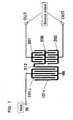
- FIG. 7is a view showing improvements with respect to the electrode structure shown in FIG. 3;
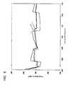
- FIG. 8is data designating improvements in a phase difference between balanced output terminal pair OUT 1 , OUT 2 by forming the electrode structure of FIG. 7;
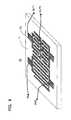
- FIG. 9is a view showing a perspective view of the surface acoustic wave device in which the electrode structure of FIG. 8 is formed on the piezoelectric substrate 11 ;
- FIG. 10is a view showing a configuration that a connection part of IDT 201 and IDT 202 is connected to ground by the other configuration instead of an electrode 213 of FIG. 9;
- FIG. 11is a view showing the surface acoustic wave device according to a second embodiment of the present invention.
- FIG. 12is a view showing the surface acoustic wave device according to a third embodiment of the present invention.
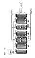
- FIG. 13is a view showing the surface acoustic wave device according to a fourth embodiment of the present invention.
- FIG. 14is a view showing the surface acoustic wave device according to a fifth embodiment of the present invention.
- FIG. 15is a view showing the surface acoustic wave device according to a sixth embodiment of the present invention.
- FIG. 16is a configuration of an embodiment improving the phase difference between signals in the balanced output terminal pair OUT 1 , OUT 2 with respect to the embodiment of FIG. 15;
- FIG. 17is a view showing the surface acoustic wave device according to a seventh embodiment of the present invention.
- FIG. 18is a view showing the surface acoustic wave device according to an eighth embodiment of the present invention.
- FIG. 19is a view showing the surface acoustic wave device according to a ninth embodiment of the present invention.
- FIG. 20is an embodiment improving a phase difference between the balanced output terminal pair OUT 1 , OUT 2 in the embodiment of FIG. 19 .
- FIG. 2is a view showing an adaptive example of, a surface acoustic wave device 10 according to the present invention as a surface acoustic wave filter, which is lead to a mixer circuit IC 3 similarly to FIG. 1 .
- the surface acoustic wave filter according to the present inventionhas an unbalanced-balanced transformation function and an impedance transformation function.
- an unbalanced-balanced transformation function and an impedance transformation functionare possible to set a balanced input of the mixer circuit IC 3 to an input impedance. Accordingly, it is possible not to use the independent unbalanced-balanced transformation function and impedance transformation function circuit, which is necessary in FIG. 1 . Thus, it is possible to realize a downsizing of the device.
- FIG. 3shows an electrode structure of the surface acoustic wave device 10 according to a first embodiment of the present invention, for use in one example in FIG. 2 .
- a single input interdigital transducer (IDT) 100 and output interdigital transducer (IDT) 200are disposed on a propagation path of surface acoustic waves formed on a piezoelectric substrate to be described later in detail.
- a first interdigital electrode finger 101 a at one side of the input IDT 100is connected to an input signal terminal IN, and a counter second interdigital electrode finger 101 b is grounded.
- a width X overlapped by the first electrode finger 101 a and second electrode finger 101 bis an aperture length of the input IDT 100 .
- the output IDT 200has first and second divided interdigital transducers (IDT) 201 , 202 having aperture lengths X 1 , X 2 substantially half the aperture length X within a range of the aperture length X of the input IDT 100 .
- IDTinterdigital transducers
- One electrode finger of the first divided IDT 201 and one electrode finger of the second divided IDT 202are connected to balanced output terminal pair OUT 1 , OUT 2 , respectively, and further the other electrode fingers of the first and second divided IDTs 201 , 202 are configured so as to be commonly connected, respectively.
- the electrode fingers of the first and second IDTs 201 , 202are configured so that the positions are mutually slid by 1 cycle in a position of the electrode finger, namely by 1 ⁇ 2 of a surface acoustic wavelength.
- FIG. 4is a view constituting the surface acoustic wave device in which an electrode structure shown in FIG. 3 is disposed on a piezoelectric substrate 11 .
- the piezoelectric substrate 11is obtained by cutting out from a crystal body of LiTaO 3 , or LiNbO 3 with a predetermined rotated angle.
- an input terminal IN, a ground terminal GND, and the output terminals OUT 1 , OUT 2 of the surface acoustic wave deviceare provided in the exterior of a package (not shown), and each electrode pad 12 formed on the piezoelectric substrate 11 is connected to each terminal by a lead-out wire.
- FIG. 5is an embodiment showing another terminal structure.
- the electrode structure of FIG. 3is formed similarly to the structure of FIG. 4 .
- This structurediffers from FIG. 4 in that the input terminal IN, the ground terminal GND, and the output terminals OUT 1 , OUT 2 are connected to the electrode pads 12 by a bonding chip 13 instead of a connection by the lead-out wire.
- FIG. 6is a view for explaining an operational principle in an electrode structure of FIG. 3, and in particular, typically showing a behavior when the surface acoustic waves (hereinafter SAW) propagate between an input and output.
- SAWsurface acoustic waves
- an upside of the two divided output IDTs 201 , 202is called a track 1
- a downside thereofis called a track 2 .
- a certain moment when the surface acoustic wave device is operatingis considered.
- an input electric signalis transformed to the SAW by the input IDT 100 .
- This SAWis propagated on the piezoelectric substrate.
- the SAWis incident on each of the first and second divided IDTS 201 , 202 of the output IDT 200 as the track 1 and track 2 .
- each SAW amplitude of the tracks 1 , 2is shown.
- a balanced terminal pairis formed between the output terminal pair OUT 1 and OUT 2 , thereby realizing an unbalanced input-balanced output.
- an I/O impedancewill be considered.
- a capacitance impedanceis formed between the electrode fingers of the IDT, and a magnitude of the capacitance impedance is determined according to an interval of the electrode fingers and aperture length.
- an interval A-B between the electrode fingers of input IDT 100is equal to an interval C-D of the electrode fingers of the output IDT 200 . Accordingly, when the input impedance is 50 ⁇ , since in the impedance of the IDT 201 at a track 1 side, an aperture length X 1 of the IDT 201 is about half the aperture length X of the input IDT 100 , the impedance becomes doubled, or about 100 ⁇ .
- the impedance of the IDT 202 at the track 2 sidesimilarly becomes about 100 ⁇ . Accordingly, when viewed between the balanced output terminal pair OUT 1 and OUT 2 , since the two output IDTs 201 , 202 are serial-connected, the entire impedance at the output side becomes about 200 ⁇ . Thus, it becomes possible to transform the I/O impedance from 50 ⁇ to 200 ⁇ .
- FIG. 7is a view showing improvement with respect to the electrode structure shown in FIG. 3 .
- an electrode of the connection part of the IDT 201 and IDT 202is connected to the second electrode finger 101 b connected to the ground on one side of the input IDT 100 by the electrode 213 .
- the electrode of the connection part of the IDT 201 and IDT 202is set as the ground.
- FIG. 8is data designating improvements in a phase difference between balanced output terminal pairs OUT 1 , OUT 2 by forming such the electrode structure of FIG. 7 .
- the abscissa axisrepresents a normalized frequency and the ordinate axis represents a phase difference.
- graph Idesignates a case where the electrode of the connection part of the IDT 201 and IDT 202 is set as the ground
- graph IIdesignates an example equal to the structure shown in FIG. 3 .
- the electrode of the connection part of the IDT 201 and IDT 202is set as the ground, whereby the phase difference of the output terminals pair OUT 1 and OUT 2 can be made small.
- FIG. 9is a view showing a perspective view of the surface acoustic wave device in which such the electrode structure of FIG. 8 is formed on the piezoelectric substrate 11 .
- the connection part of the IDT 201 and IDT 202is connected to the second electrode finger 101 b of the input IDT 100 linked with the ground.
- the electrode 213functions so that the connection part of the IDT 201 and IDT 202 is connected to the ground. Accordingly, it is possible to connect the connection part of the IDT 201 and IDT 202 to the ground instead of the electrode 213 .
- FIG. 10is a view showing such other configurations.
- an electrode pad 14 linked with the connection part of the IDT 201 and the IDT 202is provided, and this electrode pad 14 is directly connected to the ground via an electrode lead. With such the configuration, it is possible to reduce the phase difference between the output terminal pair OUT 1 and OUT 2 as well.
- FIG. 11is a view showing a second embodiment of the present invention.
- FIG. 11shows an electrode finger configuration of the IDT formed on the piezoelectric substrate similarly with FIG. 3 .
- the two input IDTs 101 , 102 and the one output IDT 200 so as to be pinched therebetweenare disposed.
- both the sidescomprise reflectors 301 , 302 , forming a so-called double mode filter configuration.
- the two signals fetched out therefromare balance-output between the output terminal pairs OUT 1 and OUT 2 .
- the impedance transformation functionis same with that described previously in FIG. 6 .
- FIG. 12shows a third embodiment of the present invention, and shows the electrode finger configuration of the IDT formed on the piezoelectric substrate in the same manner as in the preceding example.
- This embodimentalso has a double mode filter configuration. It is characterized in that two combinations (IDTs 201 , 202 , and IDTS 203 , 204 ) of the IDTs are used at an output side in opposition to the embodiment of FIG. 11 .
- the same characteristic as in the second embodimentcan be obtained, and it is valid in the case where the output impedance is desired to set lower than the second embodiment. That is, as described above, the two combinations (IDTs 201 , 202 , and IDTs 203 , 204 ) of the IDTs are used, and these are parallel-connected to the balanced output terminal pairs OUT 1 , OUT 2 .
- the output impedancebecomes 100 ⁇ .
- FIG. 13shows a fourth embodiment of the present invention, and has a multi-electrode type surface acoustic wave filter comprising 5 IDTs, of which the three input IDTs 101 to 103 and two sets of the output IDTs 201 to 202 , and 203 to 204 are alternately disposed.
- the multi-electrode typecan be defined as containing a plurality of (three or more) IDTs.
- the embodiment of the double mode type of FIGS. 11 and 12corresponds to the case of containing a minimum piece of IDTS in the multi-electrode type.
- each output of the two sets of the output IDTs 201 to 202 , and 203 to 204is led to the balanced output terminal pairs OUT 1 , OUT 2 .
- FIG. 14further shows a fifth embodiment of the present invention, and shows a configuration of the electrode finger of the IDT formed on the piezoelectric substrate in the same manner as in the preceding examples.
- the fifth embodimentis same as in the embodiment of FIG. 13 in that the multi-electrode configuration is used, but the three sets of the IDTs 201 to 202 , 203 to 204 , and 205 to 205 a is used at the output side.
- the same characteristic as in FIG. 13can be obtained, and it is valid in the case where the output impedance is desired to set lower than the embodiment of FIG. 13 .
- FIG. 15shows a sixth embodiment of the present invention, and shows a configuration of the electrode finger of the IDT formed on the piezoelectric substrate in the same manner as in the preceding example.
- the multi-electrode type filteris configured by two-stage cascade-connection. That is, first stage IDTs 103 to 105 are cascade-connected to second stage IDTs 113 to 115 .
- the two sets of IDTs 201 to 202 , and 203 to 204are used as the output IDT of the filter at the second stage.
- the output of the two sets of IDTS 201 to 202 , and 203 to 204is fetched out to the balanced output terminal pairs OUT 1 , OUT 2 .
- FIG. 16is a configuration of an embodiment improving the phase difference between signals in the balanced output terminal pairs OUT 1 , OUT 2 with respect to the embodiment of FIG. 15.
- a common electrode 206 of the divided IDTs 201 , 202 and a common electrode 207 of the divided IDTs 203 , 204 , linked with the balanced output terminal pairs OUT 1 , OUT 2are connected to the ground.
- the common electrodesare connected to the ground through the neighboring IDTs 114 , 113 and IDTs 113 , 115 on both sides of the common electrode 206 and the common electrode 207 , and this reinforces the grounding more.
- phases of signals in electrodes 121 , 122 connecting the first step to the second stepdiffer at 180°, mutually. Furthermore, phases of signals in electrodes 122 , 123 differ at 180°, mutually.
- FIG. 17shows a seventh embodiment of the present invention, and shows a configuration of the electrode finger of the IDT formed on the piezoelectric substrate in the same manner as in the preceding examples.
- the seventh embodimenthas the same configuration as in the embodiment of FIG. 11 in that serial-resonators configured so as to have an IDT 110 and reflecting IDTS 111 , 112 at an input side of the double mode filter are cascade-connected.
- This embodimentis characterized in that, by setting appropriately frequencies of the serial resonator, the attenuation amount at a side of high frequencies in the vicinity of a passband can be largely taken.
- FIG. 18shows an eighth embodiment of the present invention, and shows a configuration of the electrode finger of the IDT formed on the piezoelectric substrate in the same manner as in the preceding examples.
- the embodiment of FIG. 18is extended the embodiment of FIG. 17, and is configured so that the serial resonators configured having an IDT 120 and reflecting IDTs 121 , 122 are further parallel-connected, with respect to the serial resonator configured having the IDT 110 and the reflecting IDTs 111 , 112 which are cascade-connected to a so-called ladder type filter at the input side of the double mode filter.
- the attenuation amount in the vicinity of the bandcan be largely taken without so deteriorating an insertion loss in a passing band, and a balanced filter can be realized.
- FIG. 19shows a ninth embodiment of the present invention, and shows a configuration of the electrode finger of the IDT formed on the piezoelectric substrate in the same manner as in the preceding examples.
- the double mode filteris cascade-connected.
- the double mode filter at a first stageis configured by an IDT 113 connected to an input terminal IN, output IDTs 211 , 212 , and reflecting IDTs 311 , 312 .
- the output IDTs 211 , 212 of the double mode filter at a first stageare connected to the input IDTs 101 , 102 of the double mode filter at a second stage.
- This embodimentis configured so that an output IDT 200 of the filter at a second stage is divided into the IDTS 201 , 202 .
- the insertion loss of the passbandis small, and it is possible to realize the balanced filter having high attenuation characteristic.
- FIG. 20is an embodiment improving the phase difference between the balanced output terminal pair OUT 1 , OUT 2 in the embodiment of FIG. 19 .
- the common electrode 206 of the divided IDTs 201 , 202is connected to the ground.
- the phases of the signals in the electrodes 121 , 122 connecting each stepdiffer at 180°, mutually.
- the phase difference between signals in the balanced output terminal pair OUT 1 , OUT 2is improved similarly as shown in FIG. 8 .
- the electrode fingers configuring the IDTsare formed and disposed on the piezoelectric substrate which was cut out from a crystal such as LiTaO 3 , LiNbO 3 , or the like.
- a crystalsuch as LiTaO 3 , LiNbO 3 , or the like.
- these inventors, etc.have proposed previously the piezoelectric substrate in Japanese Patent Application Laid-Open No. 8-179551. Accordingly, it is desirable that the piezoelectric substrate such-proposed previously is also used in the present invention.
- This preferable piezoelectric substrateis a 40° to 44° rotated Y-X LiTaO 3 , which is cut out from LitaO 3 single crystal rotated around the X axis at a rotated angle from the Y axis to the Z axis, the rotated angle being in a range between 40° and 44°.
- a 66° to 74° rotated Y-X LiNbO 3is also preferable, which is cut out from LiNbO 3 single crystal rotated around the X axis at a rotated angle from the Y axis to the Z axis, the rotated angle being in a range between 66° and 74°.
Landscapes
- Physics & Mathematics (AREA)
- Acoustics & Sound (AREA)
- Surface Acoustic Wave Elements And Circuit Networks Thereof (AREA)
Abstract
Description
Claims (6)
Applications Claiming Priority (3)
| Application Number | Priority Date | Filing Date | Title |
|---|---|---|---|
| JP2000-199279 | 2000-06-30 | ||
| JP2000199279 | 2000-06-30 | ||
| PCT/JP2001/005677WO2002003549A1 (en) | 2000-06-30 | 2001-06-29 | Surface acoustic wave device |
Related Parent Applications (1)
| Application Number | Title | Priority Date | Filing Date |
|---|---|---|---|
| PCT/JP2001/005677Continuation-In-PartWO2002003549A1 (en) | 2000-06-30 | 2001-06-29 | Surface acoustic wave device |
Publications (2)
| Publication Number | Publication Date |
|---|---|
| US20020079988A1 US20020079988A1 (en) | 2002-06-27 |
| US6759928B2true US6759928B2 (en) | 2004-07-06 |
Family
ID=18697321
Family Applications (1)
| Application Number | Title | Priority Date | Filing Date |
|---|---|---|---|
| US10/082,054Expired - LifetimeUS6759928B2 (en) | 2000-06-30 | 2002-02-26 | Surface acoustic wave device with divided interdigital transducers |
Country Status (6)
| Country | Link |
|---|---|
| US (1) | US6759928B2 (en) |
| EP (2) | EP1168611A2 (en) |
| KR (2) | KR20020003077A (en) |
| CN (2) | CN1172436C (en) |
| TW (2) | TW483238B (en) |
| WO (1) | WO2002003549A1 (en) |
Cited By (20)
| Publication number | Priority date | Publication date | Assignee | Title |
|---|---|---|---|---|
| US20040251776A1 (en)* | 2002-04-10 | 2004-12-16 | Maurata Manufacturing Co., Ltd. | Surface acoustic wave device and communication device incorporating same |
| US20040257172A1 (en)* | 2003-04-17 | 2004-12-23 | Edgar Schmidhammer | Duplexer with extended functionality |
| US20050057325A1 (en)* | 2002-04-19 | 2005-03-17 | Fujitsu Media Devices Limited | Surface acoustic wave device |
| US20050110599A1 (en)* | 2003-11-21 | 2005-05-26 | Hiroshi Kanasaki | Surface acoustic wave filter and wireless device that employs the same |
| US20050243071A1 (en)* | 2004-04-14 | 2005-11-03 | Kent Joel C | Acoustic touch sensor |
| US20060028298A1 (en)* | 2004-08-04 | 2006-02-09 | Hiroyuki Nakamura | Antenna duplexer, and RF module and communication apparatus using the same |
| US20070171003A1 (en)* | 2004-10-22 | 2007-07-26 | Murata Manufacturing Co., Ltd. | Balanced surface acoustic wave filter |
| US20070182511A1 (en)* | 2004-11-04 | 2007-08-09 | Murata Manufacturing Co., Ltd., | Balanced saw filter |
| US20070188271A1 (en)* | 2004-11-04 | 2007-08-16 | Murata Manufacturing Co., Ltd. | Balanced saw filter |
| US20070229193A1 (en)* | 2004-12-20 | 2007-10-04 | Murata Manufacturing Co., Ltd. | Balanced acoustic wave filter |
| US20070284966A1 (en)* | 2005-04-06 | 2007-12-13 | Murata Manufacturing Co., Ltd. | Surface wave sensor apparatus |
| US20080168638A1 (en)* | 2007-01-17 | 2008-07-17 | Rf Micro Devices, Inc. | Piezoelectric substrate for a saw device |
| US7408284B1 (en) | 2005-05-24 | 2008-08-05 | Rf Micro Devices, Inc. | Center chirping within series connected interdigitated transducers |
| US20080246560A1 (en)* | 2004-10-06 | 2008-10-09 | Epcos Ag | Saw Filter Featuring Impedance Transformation |
| US20080246552A1 (en)* | 2004-12-20 | 2008-10-09 | Teruhisa Shibahara | Balanced Acoustic Wave Filter Device |
| US20090206955A1 (en)* | 2008-02-20 | 2009-08-20 | Epson Toyocom Corporation | Surface acoustic wave device and surface acoustic wave oscillator |
| US20100066462A1 (en)* | 2007-06-06 | 2010-03-18 | Murata Manufacturing Co., Ltd. | Acoustic wave filter device |
| US20110193654A1 (en)* | 2008-11-04 | 2011-08-11 | Murata Manufacturing Co., Ltd. | Elastic wave filter device and module including the same |
| EP2447713A3 (en)* | 2010-10-29 | 2013-04-24 | Samsung Electronics Co., Ltd. | Single-input multi-output surface acoustic wave device |
| US8490260B1 (en) | 2007-01-17 | 2013-07-23 | Rf Micro Devices, Inc. | Method of manufacturing SAW device substrates |
Families Citing this family (13)
| Publication number | Priority date | Publication date | Assignee | Title |
|---|---|---|---|---|
| JP3780408B2 (en)* | 2001-01-26 | 2006-05-31 | 株式会社村田製作所 | Surface acoustic wave filter device |
| JP4049034B2 (en)* | 2002-08-22 | 2008-02-20 | 株式会社村田製作所 | Surface acoustic wave filter, communication device |
| JP4548418B2 (en)* | 2004-04-16 | 2010-09-22 | エプソントヨコム株式会社 | Balanced surface acoustic wave filter |
| DE102005020086B4 (en)* | 2005-04-29 | 2013-07-11 | Epcos Ag | Electric multiband component |
| JP4800026B2 (en)* | 2005-12-16 | 2011-10-26 | 三星電子株式会社 | Complex coefficient transversal filter and frequency converter |
| GB0601703D0 (en)* | 2006-01-27 | 2006-03-08 | Intellitect Water Ltd | Improvement To The Design And Construction Of Electrochemical Sensors |
| EP2017961A4 (en)* | 2006-05-08 | 2011-02-16 | Murata Manufacturing Co | Elastic wave filter device and duplexer |
| CN105631106B (en)* | 2015-12-25 | 2018-11-20 | 北京航天微电科技有限公司 | A kind of high-frequency sound surface wave device acoustic-electric collaboration full-wave simulation method |
| CN107041751A (en)* | 2017-04-01 | 2017-08-15 | 浙江大学 | A kind of surface acoustic wave sensor of breathing state detecting system and wireless and passive |
| CN111010142B (en)* | 2019-12-17 | 2023-03-10 | 成都频岢微电子有限公司 | Annular non-reflection grating low-insertion-loss acoustic surface filter |
| CN112152588B (en)* | 2020-09-25 | 2024-01-30 | 福建晶安光电有限公司 | Surface acoustic wave filter and method for processing wafer for surface acoustic wave filter |
| CN112683975A (en)* | 2020-12-18 | 2021-04-20 | 天津理工大学 | Interdigital microelectrode array electrochemical sensor, preparation method, application and special test box |
| WO2022251596A1 (en)* | 2021-05-27 | 2022-12-01 | The Regents Of The University Of California | Unapodization |
Citations (7)
| Publication number | Priority date | Publication date | Assignee | Title |
|---|---|---|---|---|
| US4425554A (en)* | 1981-01-19 | 1984-01-10 | Tokyo Shibaura Denki Kabushiki Kaisha | Surface acoustic wave resonator device |
| JPH09167936A (en) | 1995-10-13 | 1997-06-24 | Fujitsu Ltd | Surface acoustic wave device |
| JPH09205342A (en)* | 1996-01-26 | 1997-08-05 | Matsushita Electric Ind Co Ltd | Surface acoustic wave filter |
| JPH10173470A (en)* | 1996-12-09 | 1998-06-26 | Matsushita Electric Ind Co Ltd | Surface acoustic wave device |
| WO1998057429A1 (en)* | 1997-06-09 | 1998-12-17 | Epcos Ag | Dual-mode surface wave filter |
| JP2000091883A (en) | 1998-09-11 | 2000-03-31 | Hitachi Media Electoronics Co Ltd | Surface acoustic wave filter |
| JP2001292050A (en)* | 2000-04-10 | 2001-10-19 | Matsushita Electric Ind Co Ltd | Surface acoustic wave filter |
Family Cites Families (3)
| Publication number | Priority date | Publication date | Assignee | Title |
|---|---|---|---|---|
| US6104260A (en)* | 1997-12-22 | 2000-08-15 | Matsushita Electric Industrial Co., Ltd. | Surface acoustic wave filter with first and second filter tracks and balanced or unbalanced terminals |
| DE19818826B4 (en)* | 1998-04-27 | 2004-11-04 | Epcos Ag | Surface wave filters with increased bandwidth |
| JP3384403B2 (en)* | 2001-03-01 | 2003-03-10 | 株式会社村田製作所 | Surface acoustic wave device, communication device |
- 2001
- 2001-02-23TWTW090104259Apatent/TW483238B/enactive
- 2001-03-13KRKR1020010012822Apatent/KR20020003077A/ennot_activeWithdrawn
- 2001-05-10EPEP01304209Apatent/EP1168611A2/ennot_activeWithdrawn
- 2001-06-29TWTW090116006Apatent/TW536867B/ennot_activeIP Right Cessation
- 2001-06-29CNCNB018025390Apatent/CN1172436C/ennot_activeExpired - Fee Related
- 2001-06-29EPEP01945733Apatent/EP1221769A4/ennot_activeWithdrawn
- 2001-06-29KRKR1020027002742Apatent/KR20020029937A/ennot_activeCeased
- 2001-06-29WOPCT/JP2001/005677patent/WO2002003549A1/ennot_activeApplication Discontinuation
- 2001-07-02CNCN01122556Apatent/CN1337778A/enactivePending
- 2002
- 2002-02-26USUS10/082,054patent/US6759928B2/ennot_activeExpired - Lifetime
Patent Citations (10)
| Publication number | Priority date | Publication date | Assignee | Title |
|---|---|---|---|---|
| US4425554A (en)* | 1981-01-19 | 1984-01-10 | Tokyo Shibaura Denki Kabushiki Kaisha | Surface acoustic wave resonator device |
| JPH09167936A (en) | 1995-10-13 | 1997-06-24 | Fujitsu Ltd | Surface acoustic wave device |
| US6037847A (en)* | 1995-10-13 | 2000-03-14 | Fujitsu Limited | Surface acoustic wave device using a leaky surface acoustic wave with an optimized cut angle of a piezoelectric substrate |
| JPH09205342A (en)* | 1996-01-26 | 1997-08-05 | Matsushita Electric Ind Co Ltd | Surface acoustic wave filter |
| US5936488A (en)* | 1996-01-26 | 1999-08-10 | Matsushita Electric Industrial Co., Ltd. | Surface acoustic wave filter having input and output transducers with different aperture lengths |
| JPH10173470A (en)* | 1996-12-09 | 1998-06-26 | Matsushita Electric Ind Co Ltd | Surface acoustic wave device |
| WO1998057429A1 (en)* | 1997-06-09 | 1998-12-17 | Epcos Ag | Dual-mode surface wave filter |
| US6353372B1 (en)* | 1997-06-09 | 2002-03-05 | Epcos Ag | Dual-mode surface acoustic wave filter with split input/output converters determining impedance |
| JP2000091883A (en) | 1998-09-11 | 2000-03-31 | Hitachi Media Electoronics Co Ltd | Surface acoustic wave filter |
| JP2001292050A (en)* | 2000-04-10 | 2001-10-19 | Matsushita Electric Ind Co Ltd | Surface acoustic wave filter |
Cited By (56)
| Publication number | Priority date | Publication date | Assignee | Title |
|---|---|---|---|---|
| US20040251776A1 (en)* | 2002-04-10 | 2004-12-16 | Maurata Manufacturing Co., Ltd. | Surface acoustic wave device and communication device incorporating same |
| US6963156B2 (en)* | 2002-04-10 | 2005-11-08 | Murata Manufacturing Co., Ltd. | Surface acoustic wave device and communication device incorporating same |
| US6965282B2 (en)* | 2002-04-19 | 2005-11-15 | Fujitsu Media Devices Limited | Surface acoustic wave device with two split interdigital transducers connected by specified electrode structures |
| US20050057325A1 (en)* | 2002-04-19 | 2005-03-17 | Fujitsu Media Devices Limited | Surface acoustic wave device |
| US20040257172A1 (en)* | 2003-04-17 | 2004-12-23 | Edgar Schmidhammer | Duplexer with extended functionality |
| US7102460B2 (en)* | 2003-04-17 | 2006-09-05 | Epcos Ag | Duplexer with extended functionality |
| US20050110599A1 (en)* | 2003-11-21 | 2005-05-26 | Hiroshi Kanasaki | Surface acoustic wave filter and wireless device that employs the same |
| US7292122B2 (en)* | 2003-11-21 | 2007-11-06 | Fujitsu Media Devices Limited | Surface acoustic wave filter and wireless device that employs the same |
| US8941624B2 (en) | 2004-04-14 | 2015-01-27 | Touch Panel Systems, K.K. | Acoustic touch sensor utilizing edge waves |
| US9310939B2 (en) | 2004-04-14 | 2016-04-12 | Elo Touch Solutions, Inc. | Acoustic touch sensor |
| US20050248548A1 (en)* | 2004-04-14 | 2005-11-10 | Masahiro Tsumura | Acoustic touch sensor |
| US20050243071A1 (en)* | 2004-04-14 | 2005-11-03 | Kent Joel C | Acoustic touch sensor |
| US8854339B2 (en) | 2004-04-14 | 2014-10-07 | Elo Touch Solutions, Inc. | Acoustic touch sensor |
| US7545365B2 (en) | 2004-04-14 | 2009-06-09 | Tyco Electronics Corporation | Acoustic touch sensor |
| US8325159B2 (en) | 2004-04-14 | 2012-12-04 | Elo Touch Solutions, Inc. | Acoustic touch sensor |
| US20050248547A1 (en)* | 2004-04-14 | 2005-11-10 | Kent Joel C | Acoustic touch sensor |
| US7701311B2 (en) | 2004-08-04 | 2010-04-20 | Panasonic Corporation | Antenna duplexer, and RF module and communication apparatus using the same |
| US20100156554A1 (en)* | 2004-08-04 | 2010-06-24 | Hiroyuki Nakamura | Antenna duplexer, and rf module and communication apparatus using the same |
| US20060028298A1 (en)* | 2004-08-04 | 2006-02-09 | Hiroyuki Nakamura | Antenna duplexer, and RF module and communication apparatus using the same |
| US7446629B2 (en)* | 2004-08-04 | 2008-11-04 | Matsushita Electric Industrial Co., Ltd. | Antenna duplexer, and RF module and communication apparatus using the same |
| US20090002096A1 (en)* | 2004-08-04 | 2009-01-01 | Hiroyuki Nakamura | Antenna duplexer, and rf module and communication apparatus using the same |
| US8068001B2 (en) | 2004-10-06 | 2011-11-29 | Epcos Ag | Saw filter featuring impedance transformation |
| US20080246560A1 (en)* | 2004-10-06 | 2008-10-09 | Epcos Ag | Saw Filter Featuring Impedance Transformation |
| US7369015B2 (en) | 2004-10-22 | 2008-05-06 | Murata Manufacturing Co., Ltd. | Balanced surface acoustic wave filter |
| US20070171003A1 (en)* | 2004-10-22 | 2007-07-26 | Murata Manufacturing Co., Ltd. | Balanced surface acoustic wave filter |
| US7358832B2 (en) | 2004-11-04 | 2008-04-15 | Murata Manufacturing Co., Ltd. | Balanced saw filter |
| US7369016B2 (en) | 2004-11-04 | 2008-05-06 | Murata Manufacturing Co., Ltd. | Balanced saw filter |
| US20070188271A1 (en)* | 2004-11-04 | 2007-08-16 | Murata Manufacturing Co., Ltd. | Balanced saw filter |
| US20070182511A1 (en)* | 2004-11-04 | 2007-08-09 | Murata Manufacturing Co., Ltd., | Balanced saw filter |
| US20080246552A1 (en)* | 2004-12-20 | 2008-10-09 | Teruhisa Shibahara | Balanced Acoustic Wave Filter Device |
| US7528683B2 (en)* | 2004-12-20 | 2009-05-05 | Murata Manufacturing Co., Ltd. | Balanced acoustic wave filter device |
| US7429905B2 (en) | 2004-12-20 | 2008-09-30 | Murata Manufacturing Co., Ltd. | Balanced acoustic wave filter |
| US20070229193A1 (en)* | 2004-12-20 | 2007-10-04 | Murata Manufacturing Co., Ltd. | Balanced acoustic wave filter |
| US20070284966A1 (en)* | 2005-04-06 | 2007-12-13 | Murata Manufacturing Co., Ltd. | Surface wave sensor apparatus |
| US7656070B2 (en) | 2005-04-06 | 2010-02-02 | Murata Manufacturing Co., Ltd. | Surface wave sensor apparatus |
| US7521837B1 (en) | 2005-05-24 | 2009-04-21 | Rf Micro Devices, Inc. | Saw architecture with series connected interdigitated transducers |
| US8225470B1 (en) | 2005-05-24 | 2012-07-24 | Rf Micro Devices, Inc. | Process of making series connected interdigitated transducers with center chirping |
| US7849582B1 (en) | 2005-05-24 | 2010-12-14 | Rf Micro Devices, Inc. | SAW architecture with series connected interdigitated transducers |
| US7408284B1 (en) | 2005-05-24 | 2008-08-05 | Rf Micro Devices, Inc. | Center chirping within series connected interdigitated transducers |
| US7449813B1 (en) | 2005-05-24 | 2008-11-11 | Rf Micro Devices, Inc. | Interleaved interdigitated transducers |
| US8529986B1 (en) | 2005-05-24 | 2013-09-10 | Rf Micro Devices, Inc. | Layer acoustic wave device and method of making the same |
| US7528684B1 (en) | 2005-05-24 | 2009-05-05 | Rf Micro Devices, Inc. | Edge chirping within series connected interdigitated transducers |
| US8069542B1 (en) | 2005-05-24 | 2011-12-06 | Rf Micro Devices, Inc. | Interleaved interdigitated transducers |
| US8490260B1 (en) | 2007-01-17 | 2013-07-23 | Rf Micro Devices, Inc. | Method of manufacturing SAW device substrates |
| US8011074B2 (en) | 2007-01-17 | 2011-09-06 | Rf Micro Devices, Inc. | Method for manufacture of piezoelectric substrate for a saw device |
| US20080168638A1 (en)* | 2007-01-17 | 2008-07-17 | Rf Micro Devices, Inc. | Piezoelectric substrate for a saw device |
| US8102225B2 (en)* | 2007-06-06 | 2012-01-24 | Murata Manufacturing Co., Ltd. | Acoustic wave filter device |
| US20100066462A1 (en)* | 2007-06-06 | 2010-03-18 | Murata Manufacturing Co., Ltd. | Acoustic wave filter device |
| US20120068791A1 (en)* | 2008-02-20 | 2012-03-22 | Seiko Epson Corporation | Surface acoustic wave device and surface acoustic wave oscillator |
| US8084918B2 (en)* | 2008-02-20 | 2011-12-27 | Seiko Epson Corporation | Surface acoustic wave device and surface acoustic wave oscillator |
| US8237326B2 (en)* | 2008-02-20 | 2012-08-07 | Seiko Epson Corporation | Surface acoustic wave device and surface acoustic wave oscillator |
| US20090206955A1 (en)* | 2008-02-20 | 2009-08-20 | Epson Toyocom Corporation | Surface acoustic wave device and surface acoustic wave oscillator |
| US8063534B2 (en)* | 2008-02-20 | 2011-11-22 | Seiko Epson Corporation | Surface acoustic wave device and surface acoustic wave oscillator |
| US8319585B2 (en)* | 2008-11-04 | 2012-11-27 | Murata Manufacturing Co., Ltd. | Elastic wave filter device and module including the same |
| US20110193654A1 (en)* | 2008-11-04 | 2011-08-11 | Murata Manufacturing Co., Ltd. | Elastic wave filter device and module including the same |
| EP2447713A3 (en)* | 2010-10-29 | 2013-04-24 | Samsung Electronics Co., Ltd. | Single-input multi-output surface acoustic wave device |
Also Published As
| Publication number | Publication date |
|---|---|
| WO2002003549A1 (en) | 2002-01-10 |
| TW536867B (en) | 2003-06-11 |
| TW483238B (en) | 2002-04-11 |
| EP1221769A1 (en) | 2002-07-10 |
| KR20020003077A (en) | 2002-01-10 |
| CN1389017A (en) | 2003-01-01 |
| EP1168611A2 (en) | 2002-01-02 |
| KR20020029937A (en) | 2002-04-20 |
| US20020079988A1 (en) | 2002-06-27 |
| EP1221769A4 (en) | 2005-04-20 |
| CN1337778A (en) | 2002-02-27 |
| CN1172436C (en) | 2004-10-20 |
Similar Documents
| Publication | Publication Date | Title |
|---|---|---|
| US6759928B2 (en) | Surface acoustic wave device with divided interdigital transducers | |
| US6744333B2 (en) | Surface acoustic wave filter device with balanced and unbalanced terminals | |
| US6606016B2 (en) | Surface acoustic wave device using two parallel connected filters with different passbands | |
| US5999069A (en) | Surface acoustic wave ladder filter having a parallel resonator with a larger electrostatic capacitance | |
| JP3480445B2 (en) | Surface acoustic wave device | |
| JP3849289B2 (en) | Surface acoustic wave device | |
| US7211925B2 (en) | Surface acoustic wave device and branching filter | |
| US5936483A (en) | Surface acoustic wave device with two filters each having capacitive impedance in the other's passband | |
| US7233219B2 (en) | Balanced output filter having specified package input and output ground metal patterns | |
| US7868716B2 (en) | Acoustic wave filter apparatus | |
| JP4548418B2 (en) | Balanced surface acoustic wave filter | |
| US6768397B2 (en) | Surface acoustic wave filter with balanced and unbalanced terminals | |
| US7746199B2 (en) | Acoustic wave device | |
| JP3743341B2 (en) | Surface acoustic wave device | |
| JPWO2008068951A1 (en) | Surface acoustic wave filter device | |
| US6963156B2 (en) | Surface acoustic wave device and communication device incorporating same | |
| JP4734751B2 (en) | Balanced surface acoustic wave filter | |
| JP2003258603A (en) | Surface acoustic wave apparatus | |
| JPH11312944A (en) | Multiple-electrode surface acoustic wave filter, and resonator type surface acoustic wave filter | |
| WO2003001668A1 (en) | Surface acoustic wave device |
Legal Events
| Date | Code | Title | Description |
|---|---|---|---|
| AS | Assignment | Owner name:FUJITSU MEDIA DEVICES LIMITED, JAPAN Free format text:ASSIGNMENT OF ASSIGNORS INTEREST;ASSIGNORS:ENDOU, GOU;KAWACHI, OSAMU;UEDA, MASANORI;AND OTHERS;REEL/FRAME:012643/0969 Effective date:20020218 | |
| STCF | Information on status: patent grant | Free format text:PATENTED CASE | |
| FEPP | Fee payment procedure | Free format text:PAYOR NUMBER ASSIGNED (ORIGINAL EVENT CODE: ASPN); ENTITY STATUS OF PATENT OWNER: LARGE ENTITY | |
| FPAY | Fee payment | Year of fee payment:4 | |
| AS | Assignment | Owner name:TAIYO YUDEN MOBILE TECHNOLOGY CO., LTD., JAPAN Free format text:ASSIGNMENT OF ASSIGNORS INTEREST;ASSIGNOR:FUJITSU MEDIA DEVICES LIMITED;REEL/FRAME:025095/0167 Effective date:20100331 | |
| AS | Assignment | Owner name:TAIYO YUDEN CO., LTD., JAPAN Free format text:ASSIGNMENT OF ASSIGNORS INTEREST;ASSIGNOR:TAIYO YUDEN MOBILE TECHNOLOGY CO., LTD.;REEL/FRAME:025095/0893 Effective date:20100331 | |
| FPAY | Fee payment | Year of fee payment:8 | |
| FPAY | Fee payment | Year of fee payment:12 |