US6759275B1 - Method for making high-performance RF integrated circuits - Google Patents
Method for making high-performance RF integrated circuitsDownload PDFInfo
- Publication number
- US6759275B1 US6759275B1US09/945,436US94543601AUS6759275B1US 6759275 B1US6759275 B1US 6759275B1US 94543601 AUS94543601 AUS 94543601AUS 6759275 B1US6759275 B1US 6759275B1
- Authority
- US
- United States
- Prior art keywords
- substrate
- layer
- scribe line
- bond pads
- passive
- Prior art date
- Legal status (The legal status is an assumption and is not a legal conclusion. Google has not performed a legal analysis and makes no representation as to the accuracy of the status listed.)
- Expired - Lifetime, expires
Links
- 238000000034methodMethods0.000titleclaimsabstractdescription41
- 239000000758substrateSubstances0.000claimsabstractdescription167
- 238000002161passivationMethods0.000claimsabstractdescription42
- 239000004065semiconductorSubstances0.000claimsabstractdescription34
- 239000011521glassSubstances0.000claimsabstractdescription20
- 238000009413insulationMethods0.000claimsabstractdescription20
- 238000005520cutting processMethods0.000claimsdescription13
- 239000000463materialSubstances0.000claimsdescription9
- 238000000151depositionMethods0.000claimsdescription7
- 230000000149penetrating effectEffects0.000claimsdescription3
- 230000006698inductionEffects0.000claims1
- 229910052710siliconInorganic materials0.000abstractdescription45
- 239000010703siliconSubstances0.000abstractdescription45
- 229920000642polymerPolymers0.000abstractdescription19
- 238000005530etchingMethods0.000abstractdescription6
- 239000010410layerSubstances0.000description131
- XUIMIQQOPSSXEZ-UHFFFAOYSA-NSiliconChemical compound[Si]XUIMIQQOPSSXEZ-UHFFFAOYSA-N0.000description48
- 238000012545processingMethods0.000description18
- 230000008569processEffects0.000description16
- 235000012431wafersNutrition0.000description14
- 238000013459approachMethods0.000description13
- 230000003071parasitic effectEffects0.000description10
- VYPSYNLAJGMNEJ-UHFFFAOYSA-NSilicium dioxideChemical compoundO=[Si]=OVYPSYNLAJGMNEJ-UHFFFAOYSA-N0.000description9
- 229910001218Gallium arsenideInorganic materials0.000description7
- 239000004642PolyimideSubstances0.000description6
- KWYUFKZDYYNOTN-UHFFFAOYSA-MPotassium hydroxideChemical compound[OH-].[K+]KWYUFKZDYYNOTN-UHFFFAOYSA-M0.000description6
- 229910052581Si3N4Inorganic materials0.000description6
- 239000004020conductorSubstances0.000description6
- 229910052751metalInorganic materials0.000description6
- 239000002184metalSubstances0.000description6
- 229920001721polyimidePolymers0.000description6
- 230000008901benefitEffects0.000description5
- 230000000694effectsEffects0.000description5
- 230000001965increasing effectEffects0.000description5
- HQVNEWCFYHHQES-UHFFFAOYSA-Nsilicon nitrideChemical compoundN12[Si]34N5[Si]62N3[Si]51N64HQVNEWCFYHHQES-UHFFFAOYSA-N0.000description5
- 239000002390adhesive tapeSubstances0.000description4
- 230000001419dependent effectEffects0.000description4
- 230000008021depositionEffects0.000description4
- 238000013461designMethods0.000description4
- 230000001939inductive effectEffects0.000description4
- 239000000377silicon dioxideSubstances0.000description4
- BOTDANWDWHJENH-UHFFFAOYSA-NTetraethyl orthosilicateChemical compoundCCO[Si](OCC)(OCC)OCCBOTDANWDWHJENH-UHFFFAOYSA-N0.000description3
- 230000005672electromagnetic fieldEffects0.000description3
- 238000005516engineering processMethods0.000description3
- 239000007789gasSubstances0.000description3
- 238000004519manufacturing processMethods0.000description3
- 238000004806packaging method and processMethods0.000description3
- 239000005360phosphosilicate glassSubstances0.000description3
- 238000000623plasma-assisted chemical vapour depositionMethods0.000description3
- 229920000052poly(p-xylylene)Polymers0.000description3
- 235000012239silicon dioxideNutrition0.000description3
- IJGRMHOSHXDMSA-UHFFFAOYSA-NAtomic nitrogenChemical compoundN#NIJGRMHOSHXDMSA-UHFFFAOYSA-N0.000description2
- 239000012790adhesive layerSubstances0.000description2
- 229910052782aluminiumInorganic materials0.000description2
- XAGFODPZIPBFFR-UHFFFAOYSA-NaluminiumChemical compound[Al]XAGFODPZIPBFFR-UHFFFAOYSA-N0.000description2
- 239000005388borosilicate glassSubstances0.000description2
- 239000011248coating agentSubstances0.000description2
- 238000000576coating methodMethods0.000description2
- 230000008878couplingEffects0.000description2
- 238000010168coupling processMethods0.000description2
- 238000005859coupling reactionMethods0.000description2
- 238000013500data storageMethods0.000description2
- 230000003247decreasing effectEffects0.000description2
- 229910003460diamondInorganic materials0.000description2
- 239000010432diamondSubstances0.000description2
- 239000003989dielectric materialSubstances0.000description2
- 238000001312dry etchingMethods0.000description2
- 238000010295mobile communicationMethods0.000description2
- 238000012986modificationMethods0.000description2
- 230000004048modificationEffects0.000description2
- 229910021421monocrystalline siliconInorganic materials0.000description2
- 230000009467reductionEffects0.000description2
- 239000005368silicate glassSubstances0.000description2
- RYGMFSIKBFXOCR-UHFFFAOYSA-NCopperChemical compound[Cu]RYGMFSIKBFXOCR-UHFFFAOYSA-N0.000description1
- KRHYYFGTRYWZRS-UHFFFAOYSA-MFluoride anionChemical compound[F-]KRHYYFGTRYWZRS-UHFFFAOYSA-M0.000description1
- 239000004793PolystyreneSubstances0.000description1
- 229910003978SiClxInorganic materials0.000description1
- 229910003828SiH3Inorganic materials0.000description1
- BLRPTPMANUNPDV-UHFFFAOYSA-NSilaneChemical compound[SiH4]BLRPTPMANUNPDV-UHFFFAOYSA-N0.000description1
- 239000004809TeflonSubstances0.000description1
- 229920006362Teflon®Polymers0.000description1
- NRTOMJZYCJJWKI-UHFFFAOYSA-NTitanium nitrideChemical compound[Ti]#NNRTOMJZYCJJWKI-UHFFFAOYSA-N0.000description1
- 239000002313adhesive filmSubstances0.000description1
- 230000004888barrier functionEffects0.000description1
- 239000003990capacitorSubstances0.000description1
- 239000012159carrier gasSubstances0.000description1
- 150000001805chlorine compoundsChemical class0.000description1
- 229910052681coesiteInorganic materials0.000description1
- 238000004891communicationMethods0.000description1
- 230000002860competitive effectEffects0.000description1
- 238000010276constructionMethods0.000description1
- 238000011109contaminationMethods0.000description1
- 238000007796conventional methodMethods0.000description1
- 229910052802copperInorganic materials0.000description1
- 239000010949copperSubstances0.000description1
- 238000005336crackingMethods0.000description1
- 229910052906cristobaliteInorganic materials0.000description1
- 239000013078crystalSubstances0.000description1
- 229910021419crystalline siliconInorganic materials0.000description1
- 239000003085diluting agentSubstances0.000description1
- 229920001971elastomerPolymers0.000description1
- 239000000806elastomerSubstances0.000description1
- 230000007613environmental effectEffects0.000description1
- 239000010408filmSubstances0.000description1
- 239000004811fluoropolymerSubstances0.000description1
- 229920002313fluoropolymerPolymers0.000description1
- BHEPBYXIRTUNPN-UHFFFAOYSA-Nhydridophosphorus(.) (triplet)Chemical compound[PH]BHEPBYXIRTUNPN-UHFFFAOYSA-N0.000description1
- 239000012535impuritySubstances0.000description1
- 238000007373indentationMethods0.000description1
- 239000011810insulating materialSubstances0.000description1
- 230000010354integrationEffects0.000description1
- 150000002500ionsChemical class0.000description1
- 238000003475laminationMethods0.000description1
- 238000004518low pressure chemical vapour depositionMethods0.000description1
- 238000005459micromachiningMethods0.000description1
- 239000000203mixtureSubstances0.000description1
- 238000009740moulding (composite fabrication)Methods0.000description1
- 150000004767nitridesChemical class0.000description1
- 229910052757nitrogenInorganic materials0.000description1
- 238000000059patterningMethods0.000description1
- 230000035515penetrationEffects0.000description1
- 238000005268plasma chemical vapour depositionMethods0.000description1
- 239000004033plasticSubstances0.000description1
- 229920003023plasticPolymers0.000description1
- 229920003209poly(hydridosilsesquioxane)Polymers0.000description1
- 229920003229poly(methyl methacrylate)Polymers0.000description1
- 239000004417polycarbonateSubstances0.000description1
- 229920000515polycarbonatePolymers0.000description1
- 229920006254polymer filmPolymers0.000description1
- 239000004926polymethyl methacrylateSubstances0.000description1
- -1polyoxides (PO)Polymers0.000description1
- 238000003825pressingMethods0.000description1
- 230000001681protective effectEffects0.000description1
- 239000000376reactantSubstances0.000description1
- 229910052594sapphireInorganic materials0.000description1
- 239000010980sapphireSubstances0.000description1
- 150000003376siliconChemical class0.000description1
- 229910052814silicon oxideInorganic materials0.000description1
- 239000002210silicon-based materialSubstances0.000description1
- OLRJXMHANKMLTD-UHFFFAOYSA-NsilylChemical compound[SiH3]OLRJXMHANKMLTD-UHFFFAOYSA-N0.000description1
- 229910001415sodium ionInorganic materials0.000description1
- 238000004528spin coatingMethods0.000description1
- 229910052682stishoviteInorganic materials0.000description1
- 239000010409thin filmSubstances0.000description1
- 229910052905tridymiteInorganic materials0.000description1
- 238000001039wet etchingMethods0.000description1
Images

Classifications
- H—ELECTRICITY
- H01—ELECTRIC ELEMENTS
- H01L—SEMICONDUCTOR DEVICES NOT COVERED BY CLASS H10
- H01L23/00—Details of semiconductor or other solid state devices
- H01L23/544—Marks applied to semiconductor devices or parts, e.g. registration marks, alignment structures, wafer maps
- H—ELECTRICITY
- H01—ELECTRIC ELEMENTS
- H01L—SEMICONDUCTOR DEVICES NOT COVERED BY CLASS H10
- H01L21/00—Processes or apparatus adapted for the manufacture or treatment of semiconductor or solid state devices or of parts thereof
- H01L21/67—Apparatus specially adapted for handling semiconductor or electric solid state devices during manufacture or treatment thereof; Apparatus specially adapted for handling wafers during manufacture or treatment of semiconductor or electric solid state devices or components ; Apparatus not specifically provided for elsewhere
- H01L21/683—Apparatus specially adapted for handling semiconductor or electric solid state devices during manufacture or treatment thereof; Apparatus specially adapted for handling wafers during manufacture or treatment of semiconductor or electric solid state devices or components ; Apparatus not specifically provided for elsewhere for supporting or gripping
- H01L21/6835—Apparatus specially adapted for handling semiconductor or electric solid state devices during manufacture or treatment thereof; Apparatus specially adapted for handling wafers during manufacture or treatment of semiconductor or electric solid state devices or components ; Apparatus not specifically provided for elsewhere for supporting or gripping using temporarily an auxiliary support
- H01L21/6836—Wafer tapes, e.g. grinding or dicing support tapes
- H—ELECTRICITY
- H01—ELECTRIC ELEMENTS
- H01L—SEMICONDUCTOR DEVICES NOT COVERED BY CLASS H10
- H01L21/00—Processes or apparatus adapted for the manufacture or treatment of semiconductor or solid state devices or of parts thereof
- H01L21/70—Manufacture or treatment of devices consisting of a plurality of solid state components formed in or on a common substrate or of parts thereof; Manufacture of integrated circuit devices or of parts thereof
- H01L21/77—Manufacture or treatment of devices consisting of a plurality of solid state components or integrated circuits formed in, or on, a common substrate
- H01L21/78—Manufacture or treatment of devices consisting of a plurality of solid state components or integrated circuits formed in, or on, a common substrate with subsequent division of the substrate into plural individual devices
- H—ELECTRICITY
- H01—ELECTRIC ELEMENTS
- H01L—SEMICONDUCTOR DEVICES NOT COVERED BY CLASS H10
- H01L23/00—Details of semiconductor or other solid state devices
- H01L23/52—Arrangements for conducting electric current within the device in operation from one component to another, i.e. interconnections, e.g. wires, lead frames
- H01L23/522—Arrangements for conducting electric current within the device in operation from one component to another, i.e. interconnections, e.g. wires, lead frames including external interconnections consisting of a multilayer structure of conductive and insulating layers inseparably formed on the semiconductor body
- H01L23/5227—Inductive arrangements or effects of, or between, wiring layers
- H—ELECTRICITY
- H10—SEMICONDUCTOR DEVICES; ELECTRIC SOLID-STATE DEVICES NOT OTHERWISE PROVIDED FOR
- H10D—INORGANIC ELECTRIC SEMICONDUCTOR DEVICES
- H10D1/00—Resistors, capacitors or inductors
- H10D1/20—Inductors
- H—ELECTRICITY
- H01—ELECTRIC ELEMENTS
- H01L—SEMICONDUCTOR DEVICES NOT COVERED BY CLASS H10
- H01L2221/00—Processes or apparatus adapted for the manufacture or treatment of semiconductor or solid state devices or of parts thereof covered by H01L21/00
- H01L2221/67—Apparatus for handling semiconductor or electric solid state devices during manufacture or treatment thereof; Apparatus for handling wafers during manufacture or treatment of semiconductor or electric solid state devices or components; Apparatus not specifically provided for elsewhere
- H01L2221/683—Apparatus for handling semiconductor or electric solid state devices during manufacture or treatment thereof; Apparatus for handling wafers during manufacture or treatment of semiconductor or electric solid state devices or components; Apparatus not specifically provided for elsewhere for supporting or gripping
- H01L2221/68304—Apparatus for handling semiconductor or electric solid state devices during manufacture or treatment thereof; Apparatus for handling wafers during manufacture or treatment of semiconductor or electric solid state devices or components; Apparatus not specifically provided for elsewhere for supporting or gripping using temporarily an auxiliary support
- H01L2221/68327—Apparatus for handling semiconductor or electric solid state devices during manufacture or treatment thereof; Apparatus for handling wafers during manufacture or treatment of semiconductor or electric solid state devices or components; Apparatus not specifically provided for elsewhere for supporting or gripping using temporarily an auxiliary support used during dicing or grinding
- H—ELECTRICITY
- H01—ELECTRIC ELEMENTS
- H01L—SEMICONDUCTOR DEVICES NOT COVERED BY CLASS H10
- H01L2221/00—Processes or apparatus adapted for the manufacture or treatment of semiconductor or solid state devices or of parts thereof covered by H01L21/00
- H01L2221/67—Apparatus for handling semiconductor or electric solid state devices during manufacture or treatment thereof; Apparatus for handling wafers during manufacture or treatment of semiconductor or electric solid state devices or components; Apparatus not specifically provided for elsewhere
- H01L2221/683—Apparatus for handling semiconductor or electric solid state devices during manufacture or treatment thereof; Apparatus for handling wafers during manufacture or treatment of semiconductor or electric solid state devices or components; Apparatus not specifically provided for elsewhere for supporting or gripping
- H01L2221/68304—Apparatus for handling semiconductor or electric solid state devices during manufacture or treatment thereof; Apparatus for handling wafers during manufacture or treatment of semiconductor or electric solid state devices or components; Apparatus not specifically provided for elsewhere for supporting or gripping using temporarily an auxiliary support
- H01L2221/6834—Apparatus for handling semiconductor or electric solid state devices during manufacture or treatment thereof; Apparatus for handling wafers during manufacture or treatment of semiconductor or electric solid state devices or components; Apparatus not specifically provided for elsewhere for supporting or gripping using temporarily an auxiliary support used to protect an active side of a device or wafer
- H—ELECTRICITY
- H01—ELECTRIC ELEMENTS
- H01L—SEMICONDUCTOR DEVICES NOT COVERED BY CLASS H10
- H01L2221/00—Processes or apparatus adapted for the manufacture or treatment of semiconductor or solid state devices or of parts thereof covered by H01L21/00
- H01L2221/67—Apparatus for handling semiconductor or electric solid state devices during manufacture or treatment thereof; Apparatus for handling wafers during manufacture or treatment of semiconductor or electric solid state devices or components; Apparatus not specifically provided for elsewhere
- H01L2221/683—Apparatus for handling semiconductor or electric solid state devices during manufacture or treatment thereof; Apparatus for handling wafers during manufacture or treatment of semiconductor or electric solid state devices or components; Apparatus not specifically provided for elsewhere for supporting or gripping
- H01L2221/68304—Apparatus for handling semiconductor or electric solid state devices during manufacture or treatment thereof; Apparatus for handling wafers during manufacture or treatment of semiconductor or electric solid state devices or components; Apparatus not specifically provided for elsewhere for supporting or gripping using temporarily an auxiliary support
- H01L2221/6835—Apparatus for handling semiconductor or electric solid state devices during manufacture or treatment thereof; Apparatus for handling wafers during manufacture or treatment of semiconductor or electric solid state devices or components; Apparatus not specifically provided for elsewhere for supporting or gripping using temporarily an auxiliary support used as a support during build up manufacturing of active devices
- H—ELECTRICITY
- H01—ELECTRIC ELEMENTS
- H01L—SEMICONDUCTOR DEVICES NOT COVERED BY CLASS H10
- H01L2924/00—Indexing scheme for arrangements or methods for connecting or disconnecting semiconductor or solid-state bodies as covered by H01L24/00
- H01L2924/0001—Technical content checked by a classifier
- H01L2924/0002—Not covered by any one of groups H01L24/00, H01L24/00 and H01L2224/00
- H—ELECTRICITY
- H01—ELECTRIC ELEMENTS
- H01L—SEMICONDUCTOR DEVICES NOT COVERED BY CLASS H10
- H01L2924/00—Indexing scheme for arrangements or methods for connecting or disconnecting semiconductor or solid-state bodies as covered by H01L24/00
- H01L2924/10—Details of semiconductor or other solid state devices to be connected
- H01L2924/11—Device type
- H01L2924/12—Passive devices, e.g. 2 terminal devices
- H01L2924/1204—Optical Diode
- H01L2924/12044—OLED
- H—ELECTRICITY
- H01—ELECTRIC ELEMENTS
- H01L—SEMICONDUCTOR DEVICES NOT COVERED BY CLASS H10
- H01L2924/00—Indexing scheme for arrangements or methods for connecting or disconnecting semiconductor or solid-state bodies as covered by H01L24/00
- H01L2924/10—Details of semiconductor or other solid state devices to be connected
- H01L2924/11—Device type
- H01L2924/14—Integrated circuits
- H01L2924/141—Analog devices
- H01L2924/1423—Monolithic Microwave Integrated Circuit [MMIC]
- H—ELECTRICITY
- H01—ELECTRIC ELEMENTS
- H01L—SEMICONDUCTOR DEVICES NOT COVERED BY CLASS H10
- H01L2924/00—Indexing scheme for arrangements or methods for connecting or disconnecting semiconductor or solid-state bodies as covered by H01L24/00
- H01L2924/19—Details of hybrid assemblies other than the semiconductor or other solid state devices to be connected
- H01L2924/1901—Structure
- H01L2924/1904—Component type
- H01L2924/19041—Component type being a capacitor
- H—ELECTRICITY
- H01—ELECTRIC ELEMENTS
- H01L—SEMICONDUCTOR DEVICES NOT COVERED BY CLASS H10
- H01L2924/00—Indexing scheme for arrangements or methods for connecting or disconnecting semiconductor or solid-state bodies as covered by H01L24/00
- H01L2924/19—Details of hybrid assemblies other than the semiconductor or other solid state devices to be connected
- H01L2924/1901—Structure
- H01L2924/1904—Component type
- H01L2924/19042—Component type being an inductor
- H—ELECTRICITY
- H01—ELECTRIC ELEMENTS
- H01L—SEMICONDUCTOR DEVICES NOT COVERED BY CLASS H10
- H01L2924/00—Indexing scheme for arrangements or methods for connecting or disconnecting semiconductor or solid-state bodies as covered by H01L24/00
- H01L2924/19—Details of hybrid assemblies other than the semiconductor or other solid state devices to be connected
- H01L2924/1901—Structure
- H01L2924/1904—Component type
- H01L2924/19043—Component type being a resistor
- H—ELECTRICITY
- H01—ELECTRIC ELEMENTS
- H01L—SEMICONDUCTOR DEVICES NOT COVERED BY CLASS H10
- H01L2924/00—Indexing scheme for arrangements or methods for connecting or disconnecting semiconductor or solid-state bodies as covered by H01L24/00
- H01L2924/30—Technical effects
- H01L2924/301—Electrical effects
- H01L2924/30105—Capacitance
- H—ELECTRICITY
- H01—ELECTRIC ELEMENTS
- H01L—SEMICONDUCTOR DEVICES NOT COVERED BY CLASS H10
- H01L2924/00—Indexing scheme for arrangements or methods for connecting or disconnecting semiconductor or solid-state bodies as covered by H01L24/00
- H01L2924/30—Technical effects
- H01L2924/301—Electrical effects
- H01L2924/3011—Impedance
Definitions
- the inventionrelates to the manufacturing of high performance Integrated Circuit (IC's), and, more specifically, to methods of creating a high performance electrical inductor on the surface of a semiconductor substrate by reducing the electromagnetic losses that are typically incurred in the surface of the substrate.
- ICIntegrated Circuit
- a typical application for inductors of the inventionis in the field of modern mobile communication applications that make use of compact, high frequency equipment. Continued improvements in the performance characteristics of this equipment has over the years been achieved, further improvements will place continued emphasis on lowering the power consumption of the equipment, on reducing the size of the equipment, on increasing the operational frequency of the applications and on creating low noise levels.
- RF amplifierscontain a number of standard components, a major component of a typical RF amplifier is a tuned circuit that contains inductive and capacitive components.
- Tuned circuitsform, dependent on and determined by the values of their inductive and capacitive components, an impedance that is frequency dependent, enabling the tuned circuit to either present a high or a low impedance for signals of a certain frequency.
- the tuned circuitcan therefore either reject or pass and further amplify components of an analog signal, based on the frequency of that component.
- the tuned circuitcan in this manner be used as a filter to filter out or remove signals of certain frequencies or to remove noise from a circuit configuration that is aimed at processing analog signals.
- the tuned circuitcan also be used to form a high electrical impedance by using the LC resonance of the circuit and to thereby counteract the effects of parasitic capacitances that are part of a circuit.
- the electromagnetic field that is generated by the inductorinduces eddy currents in the underlying silicon substrate. Since the silicon substrate is a resistive conductor, the eddy currents will consume electromagnetic energy resulting in significant energy loss, resulting in a low Q inductor. This is the main reason for a low Q value of an inductor, whereby the resonant frequency of 1/(LC) limits the upper boundary of the frequency. In addition, the eddy currents that are induced by the inductor will interfere with the performance of circuitry that is in close physical proximity to the inductor.
- inductorthat forms part of an LC resonance circuit.
- the creation of the inductormust incorporate the minimization of the surface area that is required for the inductor while at the same time maintaining a high Q value for the inductor.
- inductors that are created on the surface of a substrateare of a spiral shape, whereby the spiral is created in a plane that is parallel with the plane of the surface of the substrate.
- Conventional methods that are used to create the inductor on the surface of a substratesuffer several limitations.
- MMICMonolithic Microwave Integrated Circuits
- the spiral form of the inductor that is created on the surface of a semiconductor substrateresults, due to the physical size of the inductor, in parasitic capacitances between the inductor wiring and the underlying substrate and causes electromagnetic energy losses in the underlying resistive silicon substrate.
- parasitic capacitanceshave a serious negative effect on the functionality of the created LC circuit by sharply reducing the frequency of resonance of the tuned circuit of the application. More seriously, the inductor-generated electromagnetic field will induce eddy currents in the underlying resistive silicon substrate, causing a significant energy loss that results in low Q inductors.
- the performance parameter of an inductoris typically indicated is the Quality (Q) factor of the inductor.
- Esis the energy that is stored in the reactive portion of the component
- Elis the energy that is lost in the reactive portion of the component.
- the higher the quality of the componentthe closer the resistive value of the component approaches zero while the Q factor of the component approaches infinity.
- the quality factor for componentsdiffers from the quality that is associated with filters or resonators.
- the quality factorserves as a measure of the purity of the reactance (or the susceptance) of the component, which can be degraded due to the resistive silicon substrate, the resistance of the metal lines and dielectric losses. In an actual configuration, there are always some physical resistors that will dissipate power, thereby decreasing the power that can be recovered.
- the quality factor Qis dimensionless. A Q value of greater than 100 is considered very high for discrete inductors that are mounted on the surface of Printed Circuit Boards. For inductors that form part of an integrated circuit, the Q value is typically in the range between about 3 and 10.
- the parasitic capacitances that occur as part of this creationlimit the upper bound of the cut-off frequency that can be achieved for the inductor using conventional silicon processes. This limitation is, for many applications, not acceptable. Dependent on the frequency at which the LC circuit is designed to resonate, significantly larger values of quality factor, such as for instance 50 or more, must be available. Prior Art has in this been limited to creating values of higher quality factors as separate units, and in integrating these separate units with the surrounding device functions. This negates the advantages that can be obtained when using the monolithic construction of creating both the inductor and the surrounding devices on one and the same semiconductor substrate.
- the non-monolithic approachalso has the disadvantage that additional wiring is required to interconnect the sub-components of the assembly, thereby again introducing additional parasitic capacitances and resistive losses over the interconnecting wiring network.
- additional wiringis required to interconnect the sub-components of the assembly, thereby again introducing additional parasitic capacitances and resistive losses over the interconnecting wiring network.
- power consumptionis at a premium and must therefore be as low as possible.
- the effects of parasitic capacitances and resistive power losscan be partially compensated, but there are limitations to even this approach.
- These problemstake on even greater urgency with the rapid expansion of wireless applications, such as portable telephones and the like.
- Wireless communicationis a rapidly expanding market, where the integration of RF integrated circuits is one of the most important challenges.
- One of the approachesis to significantly increase the frequency of operation to for instance the range of 10 to 100 GHz. For such high frequencies, the value of the quality factor obtained from silicon-based inductors is significantly degraded.
- monolithic inductorshave been researched using other than silicon as the base for the creation of the inductors.
- Such monolithic inductorshave for instance been created using sapphire or GaAs as a base.
- These inductorshave considerably lower substrate losses than their silicon counterparts (no eddy current, hence no loss of electromagnetic energy) and therefore provide much higher Q inductors.
- theyhave lower parasitic capacitance and therefore provide higher frequency operation capabilities. Where however more complex applications are required, the need still exists to create inductors using silicon as a substrate.
- GaAsis a semi-insulating material at high frequencies, reducing the electromagnetic losses that are incurred in the surface of the GaAs substrate, thereby increasing the Q value of the inductor created on the GaAs surface.
- GaAs RF chipshowever are expensive, a process that can avoid the use of GaAs RF chips therefore offers the benefit of cost advantage.
- U.S. Pat. No. 6,043,109discloses a IC process (including inductors) where wafers are sawed on scribe lines.
- a principle objective of the inventionis to create a high-performance radio-frequency (rf) inductor over the surface of a semiconductor substrate.
- Another objective of the inventionis to reduce effects of eddy current losses that are typically incurred by an inductor that is created on the surface of a semiconductor substrate.
- a new method and structureis provided for the creation of a semiconductor inductor.
- a semiconductor substrateis provided that has been provided with a scribe line in a passive surface region of the substrate and active circuits surrounding the passive region on the surface of the substrate.
- At least one bond padis created on the passive surface of the substrate on each side of the scribe line and in close proximity to the scribe line, this at least one bond pad is connected to interconnect wires that are created on the surface of the substrate.
- a layer of insulationis deposited over the surface of the substrate, a layer of dielectric is deposited over the layer of insulation, interconnect lines can be created in the layer of dielectric, at least one bond pad is provided on the surface of the layer of dielectric on each side of the scribe line. At least one inductor is created on each side of the scribe line on the surface of the layer of dielectric, this at least one inductor is connected to the at least one bond pad that has been created on the surface of the layer of dielectric on each side of the scribe line.
- a layer of passivationis deposited over the layer of dielectric, including the surface of the created inductor and the bond pads. The substrate is attached to a glass panel by interfacing the surface of the layer of passivation with the glass panel.
- the substrateis sawed from the backside of the substrate, the cut that is made by the sawing is aligned with the scribe line that has been provided in the passive surface of the substrate.
- the silicon that remains in place in the passive surface of the substrate underneath the scribe linesis removed by etching, opening the scribe line up to the surface of the glass panel to which the substrate is attached.
- By separating the glass panel along the scribe lineseparate active units are created that contain active semiconductor devices and at least one inductor.
- the inductoris created on the surface of a thick layer of polymer that is deposited over the layer of passivation, the wafer is attached to (laminated to) a tape after which the substrate is separated into individual units.
- FIGS. 1 through 5address the first embodiment of the invention, as follows:
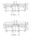
- FIG. 1is a cross section of a substrate that has been provided with an active surface region interposed by a passive surface region, the substrate has further been provided with a scribe line that is aligned with the passive surface region of the substrate.
- a layer of insulationhas been deposited over the active surface region of the substrate, at least one bond pad has been created on the surface of the passive surface region of the substrate on each side of the scribe line.
- a layer of dielectrichas been deposited over the layer of insulation partially overlying the passive surface region of the substrate, interconnect lines can be created in or on the surface of the layer of dielectric.
- At least one contact pad and at least one planar inductorhave been provided on the surface of the layer of dielectric on each side of the scribe line.
- a layer of passivationhas been created on the surface of the layer of dielectric.
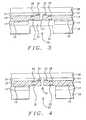
- FIG. 2shows a cross section after the structure of FIG. 1 has been attached to a glass plate.
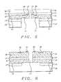
- FIG. 3shows a cross section after the backside of the substrate has been cut with a saw.
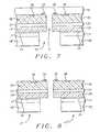
- FIG. 4shows a cross section after excess silicon has been removed from above the cut provided by the saw.
- FIG. 5shows a cross section after the unit of FIG. 4 has been divided into individual units by die sawing the glass panel.
- FIGS. 6 through 8address the second embodiment of the invention, as follows:
- FIG. 6shows a cross section of a substrate comprising at least two active surface regions separated by a passive surface region, the active surface region is insulated by a layer of insulation that is deposited over surface of the active devices contained therein.
- a layer of dielectricOn the surface of the insulating layer a layer of dielectric has been deposited. Interconnect layers are created in or on the surface of this layer of dielectric, a passivation layer has been deposited over the surface of the layer of dielectric, a thick layer of polymer dielectric has been deposited over the layer of passivation.
- a scribe linehas been provided through the layers on the surface of the substrate, at least one bond pad and at least one planar inductor have been formed on the surface of the layer of polymer on each side of the scribe line. The created planar inductor overlies the passive surface region of the substrate.
- FIG. 7shows the cross section of FIG. 6 after it has been attached to a adhesive tape.
- the substratehas been divided by sawing, creating a cut that is aligned with the scribe line whereby the cut is however wider than the scribe line.
- FIG. 8shows a cross section of the two sections that have been created by the cut as shown in FIG. 7, the two sections of substrate have been removed from the adhesive tape.
- FIG. 9shows details relating to the creation of conducting interconnects for the first embodiment of the invention.
- FIG. 10shows details relating to the creation of conducting interconnects for the second embodiment of the invention.
- active devicesare created in or on the surface of a single crystalline silicon substrate. This process of creating semiconductor devices creates multiple devices simultaneously and during one multi-step processing cycle. After the devices have been created in or on the surface of the substrate, the substrate is divided for further processing and packaging of the individual devices. Two approaches can be used for the dividing of a substrate into individual semiconductor devices, that is substrate scribing and substrate sawing.
- a diamond tipped scribeis moved across the surface of the wafer along pre-formed scribe lines (“streets”).
- the diamond scribeforms shallow scratches in the surface of the wafer.
- the waferis, with the application of pressure to the surface of the wafer, separated along the scribe lines.
- the fissures (breaks) in the waferfollow the crystal lattice structure of the wafer substrate. Scribing can be used for wafers that are about 10 mils or less in thickness. For thicker wafers, sawing is the preferred method of dicing.
- a diamond-tipped saw rotating at high rpmcontacts and saws the wafer along the streets.
- Sawingcan be performed partially or completely through the wafer.
- the waferis mounted on a supporting member such as an elastomer adhesive film or a laminated tape that is stretched across a frame.
- a number of different approacheshave been used to incorporate inductors into a semiconductor environment without sacrificing device performance due to substrate losses.
- One of these approacheshas been to selectively remove (by etching) the silicon underneath the inductor (using methods of micro machining), thereby removing substrate resistive energy losses and parasitic effects.
- Another methodhas been to use multiple layers of metal (such as aluminum) interconnects or of copper damascene interconnects.
- FIGS. 1 through 5address the first embodiment of the invention. It must hereby be pointed out and expressly emphasized that the invention is limited to post-passivation processing. In the following descriptions, the entire process of creating a high-performance rf integrated circuit, including pre-passivation layer deposition, has been highlighted in order to present the complete processing procedure. The invention however limits itself to the processing steps that are performed after a layer of passivation has been deposited over an up-to-that point created structure.
- FIG. 1there is shown a cross section of a semiconductor substrate 10 with:
- scribe line 12a scribe line; the scribe line has been created through layers overlying the substrate 10 and can reach down to the surface of the substrate 10 or can penetrate into this surface; scribe line 12 is above and approximately centered with respect to the passive region in the surface of substrate 10 ; the passive surface region of the substrate (not highlighted in FIG. 1) is therefore the surface region of substrate 10 that is interposed between regions 14
- the layer 18 of dielectricis typically used for the creation of interconnect lines in or on the surface of the layer 18 of dielectric, these interconnect lines are connected (not shown in FIG. 1) to the active devices 14 that have been created in or on the surface of substrate 10 while points of electrical contact (contact pads) are made available on both surfaces of the layer 18 of dielectric
- contact pads 20the contact pads (bond pads) in the surface of the layer 18 of dielectric, the interconnect lines that are created in or on the surface of the layer 18 of dielectric are connected to contact pads 20
- contact padscreated on the surface of the substrate 19 overlying the passive surface region of the substrate, the interconnect lines that are created in or on the surface of the layer 18 of dielectric are connected to contact pads 21
- passivation layer 24a layer of passivation that has been deposited over the surface of layer 18 of dielectric; passivation layer 24 serves the function of preventing ion and environmental contamination of the underlying circuits 14 and interconnect networks that can be created in the layer 18 of dielectric.
- the bond pads 21 and 20 and inductors 22are created on both sides of the scribe line 12
- the inductors 22are created in close proximity to the scribe line 12 ; this latter is important in view of subsequent processing steps
- the inductors 22can be connected to the interconnect lines that are created in or on the surface of the layer 18 of dielectric; more preferably, inductors 22 are connected to bond pads 20 .
- a protective film of insulationsuch as layer 16
- the layer 16 of insulationis a PECVD layer of phosphosilicate (PSG) or borophosphosilicate (BPSG), deposited in a low pressure environment at a chamber pressure of about 0.5 and 10 torr at a temperature of about 300 and 600 degrees C. with reactant gas SiH 4 at a flow rate between about 100 and 500 sccm in a diluent carrier gas PH 3 at a flow rate between about 20 and 200 sccm.
- Layer 16can be deposited to a thickness of between about 300 and 1000 Angstrom.
- Layer 18 of dielectriccan use any of the conventional dielectrics used in the industry such as for instance silicon dioxide (“oxide”, doped or undoped) or silicon nitride (“nitride”), silicon oxynitride, fluoropolymer, parylene, polyimide, tetra-ethyl-ortho-silicate (TEOS) based oxides, boro-phosphate-silicate-glass (BPSG), phospho-silicate-glass (PSG), boro-silicate-glass (BSG), oxide-nitride-oxide (ONO), plasma enhanced silicon nitride (PSiNx), oxynitride further can be used a low dielectric constant material, such as hydrogen silsesquioxane or HDP-FSG (high-density-plasma fluorine-doped silicate glass) which is a dielectric that has a lower dielectric constant than regular oxide.
- silicon dioxideoxide
- nitridesilicon nitrid
- the most commonly used and therefore the preferred dielectrics to be used for layer 18are silicon dioxide (doped or undoped), silicon oxynitride, parylene or polyimide, spin-on-glass, plasma oxide or LPCVD oxide.
- the deposition of the layer 18 of dielectricuses conventional deposition technology and can, for instance, be deposited using PECVD procedures at a temperature of between about 350 and 450 degrees C. to a thickness between about 5000 and 10,000 Angstrom using TEOS as a source.
- the passivation layer 24can contain silicon oxide/silicon nitride (SiO 2 /Si 3 N 4 ) deposited by CVD. Layer 24 can also be a photo-sensitive polyimide or can comprise titanium nitride. Another material that can be used for passivation layer 24 is phosphorous doped silicon dioxide that is typically deposited over a final layer of aluminum interconnect using a Low Temperature CVD process. Silicon nitride can be used for the passivation layer 24 due to its ability to provide an impermeable barrier to moisture and mobile impurities (e.g. sodium ions). Silicon nitride also forms a tough coating that protects underlying structures against mechanical damage.
- polyimidecan be used for passivation layer 24 . As a passivation layer, polyimide guards against thin film cracking which frequently results from the packaging of very large dies into plastic packages.
- Layer 24 of passivationcan be deposited using PECVD technology at a temperature between about 350 and 450 degrees C. with a pressure of between about 2.0 and 2.8 Torr for the duration between about 8 and 12 seconds, deposited to a thickness between about 300 and 1000 Angstrom.
- the scribe line 12plays a role in the division of the substrate 10 , which will be further discussed below. Suffice it at this time to realize that the scribe line essentially cuts through all layers overlying the surface of the substrate 10 and down to the surface of the substrate 10 .
- the inventionessentially starts with the processing step that is highlighted with the cross section that is shown in FIG. 2, which shows the cross section of FIG. 1 with however the addition of a glass panel 30 to which the construct of FIG. 1 has been attached.
- the interface between the glass panel 30 and the construct of FIG. 1is the surface of layer 24 of passivation.
- the glass panel 30can be about 200 ⁇ m thick.
- the attachment to the glass panel 30can be achieved be coating an adhesive layer over the surface of the panel, pressing the construct of FIG. 1 against this adhesive layer will result in attaching the construct of FIG. 1 to the glass panel.
- FIG. 3shows the same cross section as has been shown in FIG. 2 with the exception of a deep indentation or cut 32 that has been made into the surface of the substrate, approaching the substrate from the backside 11 . It must be noted that this cut aligns with the scribe line 12 but does not penetrate the substrate to the scribe line 12 . There remains, in other words, after cut 32 has been created, silicon material 33 present between the bottom or deepest penetration of the cut 32 and the scribe line 12 . This remaining silicon 33 has a thickness of about 10 ⁇ m and is removed by the processing step of etching the silicon 33 , FIG. 4 .
- Substrate 10can be etched from the backside 11 using a wet etchant.
- a wet etchant for a wafer that is formed of monocrystalline siliconis a solution containing a mixture of KOH (potassium hydroxide) and H 2 O. This solution anisotropically etches the silicon substrate 10 , forming grooves in the substrate having sidewalls that are sloped at an angle of about 54 degrees with the horizontal. The slope of the sidewalls is a function of the different etch rates of monocrystalline silicon along the different crystalline orientations.
- FIG. 3Another method that can be used to etch the substrate 10 in the area 33 (FIG. 3) is the use of RIE dry etching.
- bond pads 21that previously have been created in the surface of the passive surface region of the substrate 10 . These bond pads 21 are therefore available for further interconnecting of active devices of layers 14 and the planar inductors 22 .
- the inductors 22are aligned with the opening 32 that has been sawed into the backside 11 of the substrate 10 . This is of importance in view of the previously stated objective of reducing eddy currents that are typically induced in the surface of the substrate 10 by the presence of the inductors 22 . With the inductors 22 no longer overlying the surface of the silicon, since this silicon has been removed by the combined processes of sawing and etching, the objective of reducing the eddy currents in the silicon has been achieved and, with that, the objective of creating high-Q inductors for high-performance rf circuits.
- FIG. 5shows the final cross section of the first embodiment of the invention, whereby the substrate 10 has been divided into two individual units 10 ′ and 10 ′′ by sawing the glass panel 30 in alignment with the scribe line 12 . It has previously been highlighted that the inductors 22 have been created in close proximity to the scribe line 12 , the inductors 22 as a consequence are overlying layer 16 of dielectric and are no longer deposited over a layer of silicon (of the silicon substrate 10 ). Inductors 22 are therefore high-Q inductors that can be used for high-performance rf applications.
- a further and basic observation relating to FIG. 5can be made in view of the fact that the design parameters (such as the width of the cut 32 , FIG. 3) can be selected.
- the width of the opening that is created in the backside of the substrate 10can be adjusted and can be made adequately large so that, after the process of FIG. 5 has been completed, the inductors 22 are even further removed from the silicon over which the layers of insulation and the like have been deposited.
- the further the inductors are removed from the silicon of the substratethe less electromagnetic coupling between the inductors and the substrate will occur, the further eddy currents in the silicon will be reduced, the more the Q factors of the inductor will be increased.
- theses structurescan be further processed by interconnecting bond pads 21 to the surrounding circuitry, thus interconnecting the active devices 14 that have been created in or on the surface of substrate 10 and the inductors 22 to the surrounding circuitry.
- FIGS. 6 through 8address the second embodiment of the invention. Most of the processing conditions and materials used that apply to the second embodiment of the invention have been highlighted under the first embodiment of the invention and will therefore not be repeated at this time. These processing conditions and the materials that can be used for the various layers that are deposited over the surface of the substrate equally apply to the first and the second embodiment of the invention.
- FIG. 6there is shown in cross section a number of elements, some of the elements have previously been highlighted. Shown in cross section in FIG. 6 are:
- a scribe linehas been created through layers overlying the substrate 10 and can reach down to the surface of the substrate 10 or can penetrate into this surface
- the layer 18 of dielectricis typically used for the creation of interconnect lines in or on the surface of the layer 18 of dielectric, these interconnect lines are connected (not shown in FIG. 6) to the active devices 14 that have been created in or on the surface of substrate 10 while points of electrical contact (contact pads) are made available on the surfaces of layer 18
- contact padsin the surface of the layer 36 of polymer dielectric, the interconnect lines that are created in or on the surface of the layer 18 of dielectric can be connected to contact pads 20
- the polymer (SiCl x O y ) layer 36can be spun onto the surface of the passivation layer 24 and can contain but is not limited to silicons, carbons, fluoride, chlorides, oxygens, parylene, teflon, polyimide, BCB, polycarbonate (PC), polystyrene (PS), polyoxides (PO), polymethylmethacrylate (PPMA) and polypolyoxides (PPO). It is important to use a material for the polymer film that can be applied by spin coating or lamination.
- the layer 36 of polymeris typically formed to a thickness of between about 5,000 and 30,000 Angstrom.
- this layercan be cured after it has been formed. Curing can be performed at a temperature between about 250 to 450 degrees C. for a time between about 0.5 to 1.5 hours and can be performed in a vacuum or nitrogen ambient.
- FIG. 7shows the cross section of FIG. 6 after:
- the interface between the flexible tape 40 and the structure of FIG. 6is the surface of the thick layer 36 of polymer dielectric
- the substrate 10has been cut, using a saw, approaching the substrate 10 from the backside 11 and creating an opening 42 into the backside 11 of the substrate 10 .
- Opening 42aligns with the scribe line 12 and penetrates the substrate essentially to the scribe line 12 , thus separating the substrate 10 into two sections 10 ′ and 10 ′′.
- FIG. 8shows a cross section of the two units 11 ′ and 11 ′′ after the two units 11 ′ and 11 ′′ have been removed for tape 40 (FIG. 7 ).
- the removal of the tape 40exposes the inductors 22 while bond pads 20 are available for further interconnection of the units 11 ′ and 11 ′′ to surrounding circuits or as part of a semiconductor package.
- the first of these two itemsresults in a significant decrease of the eddy currents that are typically induced by overlying inductors in the underlying silicon substrate.
- the second of these itemsremoves the created inductor further from the surface of the underlying substrate, thus reducing the strength of the electromagnetic field that penetrates the underlying silicon substrate, thus further reducing the effect of electromagnetic losses in the surface of the substrate.
- the structures that are shown in cross section in FIG. 8can be further processed for conventional packaging of these structures.
- FIG. 9addresses the first embodiment of the invention, is based on FIG. 5 and provides additional detail relating to interconnect vias and interconnect lines created on the various surfaces.
- interconnect linesthat can be created in or on the surface of layer 16 of insulation; these interconnect lines 17 can be connected to the active devices in layer 14 by means of via 13
- interconnect linesthat can be created in or on the surface of layer 18 of dielectric; these interconnect lines 23 can be connected to the active devices in layer 14 by means of via 19 , interconnect lines 17 and via 15 .
- contact pads 20can be connected to interconnect lines 23 ; the planar inductors 22 can also be connected to the interconnect lines 23 . More preferably, planar inductors 22 are connected to contact pads 20 .
- FIG. 10relates to the second embodiment of the invention, that is to FIGS. 6-8.
- FIG. 10is based on FIG. 8 and provides additional detail relating to interconnect vias and interconnect lines created on the various surfaces.
- interconnect viasthat can be created through the layer 24 of passivation
- interconnect linesthat can be created in or on the surface of passivation layer 24
- interconnect viasthat can be created through the layer 36 of polymer
- interconnect linesthat can be created on the surface of layer 36 of thick polymer.
- viaor “vias” for the description of the interconnecting elements through layers of dielectric and the like as shown in FIGS. 9 and 10 does not imply that these via(s) are created as separate conducting plugs, prior to and independent of the creation of an overlying network of interconnect lines.
- the interconnection between overlying conducting layerscan be created creating an opening in the underlying layer, such as layer 18 , depositing a layer of conducting material over the underlying layer which fills the opening with a conducting material at the same time that this conducting material is deposited (for further patterning and etching, forming interconnect lines) on the surface of the underlying layer.
- vias 19can be filled with a conducting material by depositing, after openings for vias 19 have been created in layer 18 , the conducting layer 23 .
- Vias 25can be connected to interconnect lines 23 , vias 29 can be interconnected with interconnect lines 27 , bond pads 20 can be connected to interconnect lines 31 , planar inductors 22 can be connected to interconnect lines 31 but will more preferably be connected to bond pads 20 . All other elements that are shown in FIG. 9 have previously been highlighted under either FIG. 9 or FIGS. 6 through 8.
Landscapes
- Engineering & Computer Science (AREA)
- Physics & Mathematics (AREA)
- Condensed Matter Physics & Semiconductors (AREA)
- General Physics & Mathematics (AREA)
- Computer Hardware Design (AREA)
- Microelectronics & Electronic Packaging (AREA)
- Power Engineering (AREA)
- Manufacturing & Machinery (AREA)
- Semiconductor Integrated Circuits (AREA)
- Internal Circuitry In Semiconductor Integrated Circuit Devices (AREA)
Abstract
Description
Claims (11)
Priority Applications (4)
| Application Number | Priority Date | Filing Date | Title |
|---|---|---|---|
| US09/945,436US6759275B1 (en) | 2001-09-04 | 2001-09-04 | Method for making high-performance RF integrated circuits |
| US10/856,377US7319377B2 (en) | 2001-09-04 | 2004-05-28 | Method for making high-performance RF integrated circuits |
| US11/930,664US7973629B2 (en) | 2001-09-04 | 2007-10-31 | Method for making high-performance RF integrated circuits |
| US13/077,009US8384508B2 (en) | 2001-09-04 | 2011-03-31 | Method for making high-performance RF integrated circuits |
Applications Claiming Priority (1)
| Application Number | Priority Date | Filing Date | Title |
|---|---|---|---|
| US09/945,436US6759275B1 (en) | 2001-09-04 | 2001-09-04 | Method for making high-performance RF integrated circuits |
Related Child Applications (1)
| Application Number | Title | Priority Date | Filing Date |
|---|---|---|---|
| US10/856,377DivisionUS7319377B2 (en) | 2001-09-04 | 2004-05-28 | Method for making high-performance RF integrated circuits |
Publications (1)
| Publication Number | Publication Date |
|---|---|
| US6759275B1true US6759275B1 (en) | 2004-07-06 |
Family
ID=32595638
Family Applications (4)
| Application Number | Title | Priority Date | Filing Date |
|---|---|---|---|
| US09/945,436Expired - LifetimeUS6759275B1 (en) | 2001-09-04 | 2001-09-04 | Method for making high-performance RF integrated circuits |
| US10/856,377Expired - Fee RelatedUS7319377B2 (en) | 2001-09-04 | 2004-05-28 | Method for making high-performance RF integrated circuits |
| US11/930,664Expired - Fee RelatedUS7973629B2 (en) | 2001-09-04 | 2007-10-31 | Method for making high-performance RF integrated circuits |
| US13/077,009Expired - Fee RelatedUS8384508B2 (en) | 2001-09-04 | 2011-03-31 | Method for making high-performance RF integrated circuits |
Family Applications After (3)
| Application Number | Title | Priority Date | Filing Date |
|---|---|---|---|
| US10/856,377Expired - Fee RelatedUS7319377B2 (en) | 2001-09-04 | 2004-05-28 | Method for making high-performance RF integrated circuits |
| US11/930,664Expired - Fee RelatedUS7973629B2 (en) | 2001-09-04 | 2007-10-31 | Method for making high-performance RF integrated circuits |
| US13/077,009Expired - Fee RelatedUS8384508B2 (en) | 2001-09-04 | 2011-03-31 | Method for making high-performance RF integrated circuits |
Country Status (1)
| Country | Link |
|---|---|
| US (4) | US6759275B1 (en) |
Cited By (109)
| Publication number | Priority date | Publication date | Assignee | Title |
|---|---|---|---|---|
| US20030222295A1 (en)* | 1998-12-21 | 2003-12-04 | Megic Corporation | High performance system-on-chip inductor using post passivation process |
| US20040219887A1 (en)* | 1999-12-06 | 2004-11-04 | Conexant Systems, Inc. | Surface acoustic wave filter packaging |
| US20060060973A1 (en)* | 2000-10-18 | 2006-03-23 | Megic Corporation | Post passivation interconnection schemes on top of the IC chips |
| US20060205182A1 (en)* | 2005-03-10 | 2006-09-14 | Nec Electronics Corporation | Method for manufacturing semiconductor device |
| US20070108551A1 (en)* | 2003-05-27 | 2007-05-17 | Megica Corporation | High performance system-on-chip inductor using post passivation process |
| US20080035974A1 (en)* | 1998-12-21 | 2008-02-14 | Megica Corporation | High performance system-on-chip using post passivation process |
| US20080042280A1 (en)* | 2006-06-28 | 2008-02-21 | Megica Corporation | Semiconductor chip structure |
| US20080150623A1 (en)* | 2006-12-26 | 2008-06-26 | Megica Corporation | Voltage Regulator Integrated with Semiconductor Chip |
| US20080284014A1 (en)* | 2007-03-13 | 2008-11-20 | Megica Corporation | Chip assembly |
| US20090181496A1 (en)* | 2007-06-20 | 2009-07-16 | Princo Corp. | Multi-layer substrate and manufacture method thereof |
| US20100165585A1 (en)* | 2008-12-26 | 2010-07-01 | Megica Corporation | Chip packages with power management integrated circuits and related techniques |
| US7875955B1 (en) | 2006-03-09 | 2011-01-25 | National Semiconductor Corporation | On-chip power inductor |
| EP2190273A4 (en)* | 2007-07-12 | 2011-02-16 | Princo Corp | Multi-layer baseboard and manufacturing method thereof |
| US7960269B2 (en) | 2005-07-22 | 2011-06-14 | Megica Corporation | Method for forming a double embossing structure |
| US7973629B2 (en) | 2001-09-04 | 2011-07-05 | Megica Corporation | Method for making high-performance RF integrated circuits |
| US8008775B2 (en) | 2004-09-09 | 2011-08-30 | Megica Corporation | Post passivation interconnection structures |
| US8018060B2 (en) | 2004-09-09 | 2011-09-13 | Megica Corporation | Post passivation interconnection process and structures |
| US8384189B2 (en) | 2005-03-29 | 2013-02-26 | Megica Corporation | High performance system-on-chip using post passivation process |
| US8507363B2 (en) | 2011-06-15 | 2013-08-13 | Applied Materials, Inc. | Laser and plasma etch wafer dicing using water-soluble die attach film |
| US8557683B2 (en) | 2011-06-15 | 2013-10-15 | Applied Materials, Inc. | Multi-step and asymmetrically shaped laser beam scribing |
| US8557682B2 (en) | 2011-06-15 | 2013-10-15 | Applied Materials, Inc. | Multi-layer mask for substrate dicing by laser and plasma etch |
| US8598016B2 (en) | 2011-06-15 | 2013-12-03 | Applied Materials, Inc. | In-situ deposited mask layer for device singulation by laser scribing and plasma etch |
| US8642448B2 (en) | 2010-06-22 | 2014-02-04 | Applied Materials, Inc. | Wafer dicing using femtosecond-based laser and plasma etch |
| US8652940B2 (en) | 2012-04-10 | 2014-02-18 | Applied Materials, Inc. | Wafer dicing used hybrid multi-step laser scribing process with plasma etch |
| US8703581B2 (en) | 2011-06-15 | 2014-04-22 | Applied Materials, Inc. | Water soluble mask for substrate dicing by laser and plasma etch |
| US8759197B2 (en) | 2011-06-15 | 2014-06-24 | Applied Materials, Inc. | Multi-step and asymmetrically shaped laser beam scribing |
| US8845854B2 (en) | 2012-07-13 | 2014-09-30 | Applied Materials, Inc. | Laser, plasma etch, and backside grind process for wafer dicing |
| US8859397B2 (en) | 2012-07-13 | 2014-10-14 | Applied Materials, Inc. | Method of coating water soluble mask for laser scribing and plasma etch |
| US8883615B1 (en) | 2014-03-07 | 2014-11-11 | Applied Materials, Inc. | Approaches for cleaning a wafer during hybrid laser scribing and plasma etching wafer dicing processes |
| US8883614B1 (en) | 2013-05-22 | 2014-11-11 | Applied Materials, Inc. | Wafer dicing with wide kerf by laser scribing and plasma etching hybrid approach |
| US8912077B2 (en) | 2011-06-15 | 2014-12-16 | Applied Materials, Inc. | Hybrid laser and plasma etch wafer dicing using substrate carrier |
| US8912078B1 (en) | 2014-04-16 | 2014-12-16 | Applied Materials, Inc. | Dicing wafers having solder bumps on wafer backside |
| US8912075B1 (en) | 2014-04-29 | 2014-12-16 | Applied Materials, Inc. | Wafer edge warp supression for thin wafer supported by tape frame |
| US8927393B1 (en) | 2014-01-29 | 2015-01-06 | Applied Materials, Inc. | Water soluble mask formation by dry film vacuum lamination for laser and plasma dicing |
| US8932939B1 (en) | 2014-04-14 | 2015-01-13 | Applied Materials, Inc. | Water soluble mask formation by dry film lamination |
| US8940619B2 (en) | 2012-07-13 | 2015-01-27 | Applied Materials, Inc. | Method of diced wafer transportation |
| US8946057B2 (en) | 2012-04-24 | 2015-02-03 | Applied Materials, Inc. | Laser and plasma etch wafer dicing using UV-curable adhesive film |
| US8951819B2 (en) | 2011-07-11 | 2015-02-10 | Applied Materials, Inc. | Wafer dicing using hybrid split-beam laser scribing process with plasma etch |
| US8969177B2 (en) | 2012-06-29 | 2015-03-03 | Applied Materials, Inc. | Laser and plasma etch wafer dicing with a double sided UV-curable adhesive film |
| US8975163B1 (en) | 2014-04-10 | 2015-03-10 | Applied Materials, Inc. | Laser-dominated laser scribing and plasma etch hybrid wafer dicing |
| US8975162B2 (en) | 2012-12-20 | 2015-03-10 | Applied Materials, Inc. | Wafer dicing from wafer backside |
| US8980727B1 (en) | 2014-05-07 | 2015-03-17 | Applied Materials, Inc. | Substrate patterning using hybrid laser scribing and plasma etching processing schemes |
| US8980726B2 (en) | 2013-01-25 | 2015-03-17 | Applied Materials, Inc. | Substrate dicing by laser ablation and plasma etch damage removal for ultra-thin wafers |
| US8993414B2 (en) | 2012-07-13 | 2015-03-31 | Applied Materials, Inc. | Laser scribing and plasma etch for high die break strength and clean sidewall |
| US8991329B1 (en) | 2014-01-31 | 2015-03-31 | Applied Materials, Inc. | Wafer coating |
| US8999816B1 (en) | 2014-04-18 | 2015-04-07 | Applied Materials, Inc. | Pre-patterned dry laminate mask for wafer dicing processes |
| US9012305B1 (en) | 2014-01-29 | 2015-04-21 | Applied Materials, Inc. | Wafer dicing using hybrid laser scribing and plasma etch approach with intermediate non-reactive post mask-opening clean |
| US9018079B1 (en) | 2014-01-29 | 2015-04-28 | Applied Materials, Inc. | Wafer dicing using hybrid laser scribing and plasma etch approach with intermediate reactive post mask-opening clean |
| US9029242B2 (en) | 2011-06-15 | 2015-05-12 | Applied Materials, Inc. | Damage isolation by shaped beam delivery in laser scribing process |
| US9034771B1 (en) | 2014-05-23 | 2015-05-19 | Applied Materials, Inc. | Cooling pedestal for dicing tape thermal management during plasma dicing |
| US9041198B2 (en) | 2013-10-22 | 2015-05-26 | Applied Materials, Inc. | Maskless hybrid laser scribing and plasma etching wafer dicing process |
| US9048309B2 (en) | 2012-07-10 | 2015-06-02 | Applied Materials, Inc. | Uniform masking for wafer dicing using laser and plasma etch |
| US9076860B1 (en) | 2014-04-04 | 2015-07-07 | Applied Materials, Inc. | Residue removal from singulated die sidewall |
| US9093518B1 (en) | 2014-06-30 | 2015-07-28 | Applied Materials, Inc. | Singulation of wafers having wafer-level underfill |
| US9105710B2 (en) | 2013-08-30 | 2015-08-11 | Applied Materials, Inc. | Wafer dicing method for improving die packaging quality |
| US9112050B1 (en) | 2014-05-13 | 2015-08-18 | Applied Materials, Inc. | Dicing tape thermal management by wafer frame support ring cooling during plasma dicing |
| US9117868B1 (en) | 2014-08-12 | 2015-08-25 | Applied Materials, Inc. | Bipolar electrostatic chuck for dicing tape thermal management during plasma dicing |
| US9126285B2 (en) | 2011-06-15 | 2015-09-08 | Applied Materials, Inc. | Laser and plasma etch wafer dicing using physically-removable mask |
| US9130056B1 (en) | 2014-10-03 | 2015-09-08 | Applied Materials, Inc. | Bi-layer wafer-level underfill mask for wafer dicing and approaches for performing wafer dicing |
| US9130057B1 (en) | 2014-06-30 | 2015-09-08 | Applied Materials, Inc. | Hybrid dicing process using a blade and laser |
| US9129904B2 (en) | 2011-06-15 | 2015-09-08 | Applied Materials, Inc. | Wafer dicing using pulse train laser with multiple-pulse bursts and plasma etch |
| US9130030B1 (en) | 2014-03-07 | 2015-09-08 | Applied Materials, Inc. | Baking tool for improved wafer coating process |
| US9142459B1 (en) | 2014-06-30 | 2015-09-22 | Applied Materials, Inc. | Wafer dicing using hybrid laser scribing and plasma etch approach with mask application by vacuum lamination |
| US9159624B1 (en) | 2015-01-05 | 2015-10-13 | Applied Materials, Inc. | Vacuum lamination of polymeric dry films for wafer dicing using hybrid laser scribing and plasma etch approach |
| US9159621B1 (en) | 2014-04-29 | 2015-10-13 | Applied Materials, Inc. | Dicing tape protection for wafer dicing using laser scribe process |
| US9159574B2 (en) | 2012-08-27 | 2015-10-13 | Applied Materials, Inc. | Method of silicon etch for trench sidewall smoothing |
| US9165832B1 (en) | 2014-06-30 | 2015-10-20 | Applied Materials, Inc. | Method of die singulation using laser ablation and induction of internal defects with a laser |
| US9165812B2 (en) | 2014-01-31 | 2015-10-20 | Applied Materials, Inc. | Cooled tape frame lift and low contact shadow ring for plasma heat isolation |
| US9177861B1 (en) | 2014-09-19 | 2015-11-03 | Applied Materials, Inc. | Hybrid wafer dicing approach using laser scribing process based on an elliptical laser beam profile or a spatio-temporal controlled laser beam profile |
| US9196536B1 (en) | 2014-09-25 | 2015-11-24 | Applied Materials, Inc. | Hybrid wafer dicing approach using a phase modulated laser beam profile laser scribing process and plasma etch process |
| US9196498B1 (en) | 2014-08-12 | 2015-11-24 | Applied Materials, Inc. | Stationary actively-cooled shadow ring for heat dissipation in plasma chamber |
| US9224650B2 (en) | 2013-09-19 | 2015-12-29 | Applied Materials, Inc. | Wafer dicing from wafer backside and front side |
| US9236305B2 (en) | 2013-01-25 | 2016-01-12 | Applied Materials, Inc. | Wafer dicing with etch chamber shield ring for film frame wafer applications |
| US9245803B1 (en) | 2014-10-17 | 2016-01-26 | Applied Materials, Inc. | Hybrid wafer dicing approach using a bessel beam shaper laser scribing process and plasma etch process |
| US9252057B2 (en) | 2012-10-17 | 2016-02-02 | Applied Materials, Inc. | Laser and plasma etch wafer dicing with partial pre-curing of UV release dicing tape for film frame wafer application |
| US9275902B2 (en) | 2014-03-26 | 2016-03-01 | Applied Materials, Inc. | Dicing processes for thin wafers with bumps on wafer backside |
| US9281244B1 (en) | 2014-09-18 | 2016-03-08 | Applied Materials, Inc. | Hybrid wafer dicing approach using an adaptive optics-controlled laser scribing process and plasma etch process |
| US9293304B2 (en) | 2013-12-17 | 2016-03-22 | Applied Materials, Inc. | Plasma thermal shield for heat dissipation in plasma chamber |
| US9299614B2 (en) | 2013-12-10 | 2016-03-29 | Applied Materials, Inc. | Method and carrier for dicing a wafer |
| US9299611B2 (en) | 2014-01-29 | 2016-03-29 | Applied Materials, Inc. | Method of wafer dicing using hybrid laser scribing and plasma etch approach with mask plasma treatment for improved mask etch resistance |
| US9312177B2 (en) | 2013-12-06 | 2016-04-12 | Applied Materials, Inc. | Screen print mask for laser scribe and plasma etch wafer dicing process |
| US9330977B1 (en) | 2015-01-05 | 2016-05-03 | Applied Materials, Inc. | Hybrid wafer dicing approach using a galvo scanner and linear stage hybrid motion laser scribing process and plasma etch process |
| US9349648B2 (en) | 2014-07-22 | 2016-05-24 | Applied Materials, Inc. | Hybrid wafer dicing approach using a rectangular shaped two-dimensional top hat laser beam profile or a linear shaped one-dimensional top hat laser beam profile laser scribing process and plasma etch process |
| US9355907B1 (en) | 2015-01-05 | 2016-05-31 | Applied Materials, Inc. | Hybrid wafer dicing approach using a line shaped laser beam profile laser scribing process and plasma etch process |
| US9460966B2 (en) | 2013-10-10 | 2016-10-04 | Applied Materials, Inc. | Method and apparatus for dicing wafers having thick passivation polymer layer |
| US9478455B1 (en) | 2015-06-12 | 2016-10-25 | Applied Materials, Inc. | Thermal pyrolytic graphite shadow ring assembly for heat dissipation in plasma chamber |
| US9509251B2 (en) | 2015-03-24 | 2016-11-29 | Freescale Semiconductor, Inc. | RF amplifier module and methods of manufacture thereof |
| US20170033040A1 (en)* | 2006-07-21 | 2017-02-02 | Gula Consulting Limited Liability Company | High speed, high density, low power die interconnect system |
| US9601375B2 (en) | 2015-04-27 | 2017-03-21 | Applied Materials, Inc. | UV-cure pre-treatment of carrier film for wafer dicing using hybrid laser scribing and plasma etch approach |
| US9620379B2 (en) | 2013-03-14 | 2017-04-11 | Applied Materials, Inc. | Multi-layer mask including non-photodefinable laser energy absorbing layer for substrate dicing by laser and plasma etch |
| US9721839B2 (en) | 2015-06-12 | 2017-08-01 | Applied Materials, Inc. | Etch-resistant water soluble mask for hybrid wafer dicing using laser scribing and plasma etch |
| US9787254B2 (en) | 2015-09-23 | 2017-10-10 | Nxp Usa, Inc. | Encapsulated semiconductor device package with heatsink opening, and methods of manufacture thereof |
| US9793132B1 (en) | 2016-05-13 | 2017-10-17 | Applied Materials, Inc. | Etch mask for hybrid laser scribing and plasma etch wafer singulation process |
| US9852997B2 (en) | 2016-03-25 | 2017-12-26 | Applied Materials, Inc. | Hybrid wafer dicing approach using a rotating beam laser scribing process and plasma etch process |
| US9871107B2 (en) | 2015-05-22 | 2018-01-16 | Nxp Usa, Inc. | Device with a conductive feature formed over a cavity and method therefor |
| US9972575B2 (en) | 2016-03-03 | 2018-05-15 | Applied Materials, Inc. | Hybrid wafer dicing approach using a split beam laser scribing process and plasma etch process |
| US20180185964A1 (en)* | 2015-11-09 | 2018-07-05 | Furukawa Electric Co., Ltd. | Method of producing semiconductor chip, and mask-integrated surface protective tape used therein |
| US10075132B2 (en) | 2015-03-24 | 2018-09-11 | Nxp Usa, Inc. | RF amplifier with conductor-less region underlying filter circuit inductor, and methods of manufacture thereof |
| US10363629B2 (en) | 2017-06-01 | 2019-07-30 | Applied Materials, Inc. | Mitigation of particle contamination for wafer dicing processes |
| US10535561B2 (en) | 2018-03-12 | 2020-01-14 | Applied Materials, Inc. | Hybrid wafer dicing approach using a multiple pass laser scribing process and plasma etch process |
| US10692765B2 (en) | 2014-11-07 | 2020-06-23 | Applied Materials, Inc. | Transfer arm for film frame substrate handling during plasma singulation of wafers |
| US10903121B1 (en) | 2019-08-14 | 2021-01-26 | Applied Materials, Inc. | Hybrid wafer dicing approach using a uniform rotating beam laser scribing process and plasma etch process |
| US11011424B2 (en) | 2019-08-06 | 2021-05-18 | Applied Materials, Inc. | Hybrid wafer dicing approach using a spatially multi-focused laser beam laser scribing process and plasma etch process |
| US11158540B2 (en) | 2017-05-26 | 2021-10-26 | Applied Materials, Inc. | Light-absorbing mask for hybrid laser scribing and plasma etch wafer singulation process |
| US11195756B2 (en) | 2014-09-19 | 2021-12-07 | Applied Materials, Inc. | Proximity contact cover ring for plasma dicing |
| US11211247B2 (en) | 2020-01-30 | 2021-12-28 | Applied Materials, Inc. | Water soluble organic-inorganic hybrid mask formulations and their applications |
| US11342226B2 (en) | 2019-08-13 | 2022-05-24 | Applied Materials, Inc. | Hybrid wafer dicing approach using an actively-focused laser beam laser scribing process and plasma etch process |
| US11355394B2 (en) | 2018-09-13 | 2022-06-07 | Applied Materials, Inc. | Wafer dicing using hybrid laser scribing and plasma etch approach with intermediate breakthrough treatment |
| US11600492B2 (en) | 2019-12-10 | 2023-03-07 | Applied Materials, Inc. | Electrostatic chuck with reduced current leakage for hybrid laser scribing and plasma etch wafer singulation process |
Families Citing this family (16)
| Publication number | Priority date | Publication date | Assignee | Title |
|---|---|---|---|---|
| US7410894B2 (en)* | 2005-07-27 | 2008-08-12 | International Business Machines Corporation | Post last wiring level inductor using patterned plate process |
| TWI260075B (en)* | 2005-10-24 | 2006-08-11 | Via Tech Inc | Embedded inductor element and chip package applying the same |
| KR100772272B1 (en)* | 2005-12-27 | 2007-11-01 | 동부일렉트로닉스 주식회사 | Manufacturing method of MOS field effect transistor of semiconductor device |
| JP4572343B2 (en)* | 2006-03-03 | 2010-11-04 | セイコーエプソン株式会社 | Electronic substrate, semiconductor device and electronic equipment |
| US20080122039A1 (en)* | 2006-11-02 | 2008-05-29 | United Microelectronics Corp. | Intergrated circuit device, chip, and method of fabricating the same |
| KR101452548B1 (en)* | 2007-06-20 | 2014-10-21 | 스카이워크스 솔루션즈, 인코포레이티드 | Semiconductor die with backside passive device integration |
| US8680653B2 (en) | 2007-11-12 | 2014-03-25 | Infineon Technologies Ag | Wafer and a method of dicing a wafer |
| US8772156B2 (en)* | 2008-05-09 | 2014-07-08 | International Business Machines Corporation | Methods of fabricating interconnect structures containing various capping materials for electrical fuse and other related applications |
| US7956466B2 (en) | 2008-05-09 | 2011-06-07 | International Business Machines Corporation | Structure for interconnect structure containing various capping materials for electrical fuse and other related applications |
| JP5578797B2 (en)* | 2009-03-13 | 2014-08-27 | ルネサスエレクトロニクス株式会社 | Semiconductor device |
| US8436707B2 (en)* | 2010-01-12 | 2013-05-07 | Infineon Technologies Ag | System and method for integrated inductor |
| US8513771B2 (en) | 2010-06-07 | 2013-08-20 | Infineon Technologies Ag | Semiconductor package with integrated inductor |
| US9064712B2 (en) | 2010-08-12 | 2015-06-23 | Freescale Semiconductor Inc. | Monolithic microwave integrated circuit |
| US10720495B2 (en)* | 2014-06-12 | 2020-07-21 | Taiwan Semiconductor Manufacturing Company Ltd. | Semiconductor device and manufacturing method thereof |
| TWI629694B (en)* | 2015-06-25 | 2018-07-11 | 威華微機電股份有限公司 | Mass production method of preform of magnetic core inductor |
| WO2018182630A1 (en)* | 2017-03-30 | 2018-10-04 | Intel IP Corporation | Magnetic coils in locally thinned silicon bridges and methods of assembling same |
Citations (5)
| Publication number | Priority date | Publication date | Assignee | Title |
|---|---|---|---|---|
| US5387551A (en) | 1992-03-04 | 1995-02-07 | Kabushiki Kaisha Toshiba | Method of manufacturing flat inductance element |
| US5904546A (en) | 1996-02-12 | 1999-05-18 | Micron Technology, Inc. | Method and apparatus for dicing semiconductor wafers |
| US5910687A (en)* | 1997-01-24 | 1999-06-08 | Chipscale, Inc. | Wafer fabrication of die-bottom contacts for electronic devices |
| US6043109A (en) | 1999-02-09 | 2000-03-28 | United Microelectronics Corp. | Method of fabricating wafer-level package |
| US6046101A (en) | 1997-12-31 | 2000-04-04 | Intel Corporation | Passivation technology combining improved adhesion in passivation and a scribe street without passivation |
Family Cites Families (189)
| Publication number | Priority date | Publication date | Assignee | Title |
|---|---|---|---|---|
| GB1487945A (en) | 1974-11-20 | 1977-10-05 | Ibm | Semiconductor integrated circuit devices |
| US4685998A (en) | 1984-03-22 | 1987-08-11 | Thomson Components - Mostek Corp. | Process of forming integrated circuits with contact pads in a standard array |
| US4606998A (en)* | 1985-04-30 | 1986-08-19 | International Business Machines Corporation | Barrierless high-temperature lift-off process |
| US5134460A (en) | 1986-08-11 | 1992-07-28 | International Business Machines Corporation | Aluminum bump, reworkable bump, and titanium nitride structure for tab bonding |
| KR910006967B1 (en) | 1987-11-18 | 1991-09-14 | 가시오 게이상기 가부시기가이샤 | Bump electrod structure of semiconductor device and a method for forming the bump electrode |
| US5055907A (en) | 1989-01-25 | 1991-10-08 | Mosaic, Inc. | Extended integration semiconductor structure with wiring layers |
| US4885841A (en) | 1989-02-21 | 1989-12-12 | Micron Technology, Inc. | Vibrational method of aligning the leads of surface-mount electronic components with the mounting pads of printed circuit boards during the molten solder mounting process |
| US5106461A (en) | 1989-04-04 | 1992-04-21 | Massachusetts Institute Of Technology | High-density, multi-level interconnects, flex circuits, and tape for tab |
| JPH0377360A (en) | 1989-08-18 | 1991-04-02 | Mitsubishi Electric Corp | semiconductor equipment |
| EP0453785A1 (en) | 1990-04-24 | 1991-10-30 | Oerlikon Contraves AG | Method of making multilayer thin film circuit comprising integrated thin film resistors |
| US5226232A (en) | 1990-05-18 | 1993-07-13 | Hewlett-Packard Company | Method for forming a conductive pattern on an integrated circuit |
| JP3002512B2 (en) | 1990-09-10 | 2000-01-24 | 株式会社日立製作所 | Integrated circuit device |
| US5095402A (en) | 1990-10-02 | 1992-03-10 | Rogers Corporation | Internally decoupled integrated circuit package |
| US6979840B1 (en) | 1991-09-25 | 2005-12-27 | Semiconductor Energy Laboratory Co., Ltd. | Thin film transistors having anodized metal film between the gate wiring and drain wiring |
| US5336921A (en) | 1992-01-27 | 1994-08-09 | Motorola, Inc. | Vertical trench inductor |
| JPH0677407A (en) | 1992-04-06 | 1994-03-18 | Nippon Precision Circuits Kk | Semiconductor device |
| JP3063422B2 (en) | 1992-10-05 | 2000-07-12 | 富士電機株式会社 | Coil for magnetic induction element |
| WO1994017558A1 (en) | 1993-01-29 | 1994-08-04 | The Regents Of The University Of California | Monolithic passive component |
| US5328553A (en) | 1993-02-02 | 1994-07-12 | Motorola Inc. | Method for fabricating a semiconductor device having a planar surface |
| US5557180A (en) | 1993-06-30 | 1996-09-17 | Sgs-Thomson Microelectronics, Inc. | Circuit and method for operating a 3-phase motor with a uni-coil phase commutation scheme |
| US5485038A (en) | 1993-07-15 | 1996-01-16 | Hughes Aircraft Company | Microelectronic circuit substrate structure including photoimageable epoxy dielectric layers |
| US5370766A (en) | 1993-08-16 | 1994-12-06 | California Micro Devices | Methods for fabrication of thin film inductors, inductor networks and integration with other passive and active devices |
| US5416356A (en) | 1993-09-03 | 1995-05-16 | Motorola, Inc. | Integrated circuit having passive circuit elements |
| US5501006A (en) | 1993-09-22 | 1996-03-26 | Motorola, Inc. | Method for connection of signals to an integrated circuit |
| US5767564A (en) | 1993-10-19 | 1998-06-16 | Kyocera Corporation | Semiconductor device with a decoupling capacitor mounted thereon having a thermal expansion coefficient matched to the device |
| US5527998A (en) | 1993-10-22 | 1996-06-18 | Sheldahl, Inc. | Flexible multilayer printed circuit boards and methods of manufacture |
| US5455064A (en) | 1993-11-12 | 1995-10-03 | Fujitsu Limited | Process for fabricating a substrate with thin film capacitor and insulating plug |
| US5465879A (en) | 1994-01-27 | 1995-11-14 | Asymptotic Technologies, Inc. | Disposable nozzle assembly for high speed viscous material droplet dispenser |
| US5576680A (en) | 1994-03-01 | 1996-11-19 | Amer-Soi | Structure and fabrication process of inductors on semiconductor chip |
| US5478773A (en) | 1994-04-28 | 1995-12-26 | Motorola, Inc. | Method of making an electronic device having an integrated inductor |
| US5753529A (en) | 1994-05-05 | 1998-05-19 | Siliconix Incorporated | Surface mount and flip chip technology for total integrated circuit isolation |
| US5446311A (en) | 1994-09-16 | 1995-08-29 | International Business Machines Corporation | High-Q inductors in silicon technology without expensive metalization |
| US5563762A (en) | 1994-11-28 | 1996-10-08 | Northern Telecom Limited | Capacitor for an integrated circuit and method of formation thereof, and a method of adding on-chip capacitors to an integrated circuit |
| FR2728104A1 (en) | 1994-12-09 | 1996-06-14 | Sgs Thomson Microelectronics | METHOD OF MARKING CIRCUITS INTEGRATED WITH A LASER, AND MARKING APPARATUS THEREFOR |
| US5629240A (en) | 1994-12-09 | 1997-05-13 | Sun Microsystems, Inc. | Method for direct attachment of an on-chip bypass capacitor in an integrated circuit |
| US5608262A (en) | 1995-02-24 | 1997-03-04 | Lucent Technologies Inc. | Packaging multi-chip modules without wire-bond interconnection |
| EP0734059B1 (en) | 1995-03-24 | 2005-11-09 | Shinko Electric Industries Co., Ltd. | Chip sized semiconductor device and a process for making it |
| US5742100A (en) | 1995-03-27 | 1998-04-21 | Motorola, Inc. | Structure having flip-chip connected substrates |
| US5842626A (en) | 1995-03-31 | 1998-12-01 | Intel Corporation | Method for coupling surface mounted capacitors to semiconductor packages |
| US5635767A (en) | 1995-06-02 | 1997-06-03 | Motorola, Inc. | Semiconductor device having built-in high frequency bypass capacitor |
| US5608264A (en) | 1995-06-05 | 1997-03-04 | Harris Corporation | Surface mountable integrated circuit with conductive vias |
| US5656849A (en) | 1995-09-22 | 1997-08-12 | International Business Machines Corporation | Two-level spiral inductor structure having a high inductance to area ratio |
| JP2953404B2 (en) | 1995-12-08 | 1999-09-27 | ソニー株式会社 | Semiconductor device and manufacturing method thereof |
| KR0182073B1 (en) | 1995-12-22 | 1999-03-20 | 황인길 | Semiconductor chip scale semiconductor package and manufacturing method thereof |
| JP2904086B2 (en) | 1995-12-27 | 1999-06-14 | 日本電気株式会社 | Semiconductor device and manufacturing method thereof |
| US5973396A (en) | 1996-02-16 | 1999-10-26 | Micron Technology, Inc. | Surface mount IC using silicon vias in an area array format or same size as die array |
| US5686764A (en) | 1996-03-20 | 1997-11-11 | Lsi Logic Corporation | Flip chip package with reduced number of package layers |
| KR100367069B1 (en) | 1996-04-24 | 2003-03-29 | 이케다 타케시 | Semiconductor Device |
| US5883422A (en) | 1996-06-28 | 1999-03-16 | The Whitaker Corporation | Reduced parasitic capacitance semiconductor devices |
| US5949654A (en) | 1996-07-03 | 1999-09-07 | Kabushiki Kaisha Toshiba | Multi-chip module, an electronic device, and production method thereof |
| WO1998003994A1 (en) | 1996-07-18 | 1998-01-29 | Advanced Micro Devices, Inc. | Integrated circuit which uses an etch stop for producing staggered interconnect lines |
| US5793272A (en) | 1996-08-23 | 1998-08-11 | International Business Machines Corporation | Integrated circuit toroidal inductor |
| EP1014443A4 (en) | 1996-09-20 | 2001-02-07 | Tdk Corp | Passive electronic parts, ic parts, and wafer |
| US5861647A (en) | 1996-10-02 | 1999-01-19 | National Semiconductor Corporation | VLSI capacitors and high Q VLSI inductors using metal-filled via plugs |
| US5874770A (en) | 1996-10-10 | 1999-02-23 | General Electric Company | Flexible interconnect film including resistor and capacitor layers |
| US5888630A (en) | 1996-11-08 | 1999-03-30 | W. L. Gore & Associates, Inc. | Apparatus and method for unit area composition control to minimize warp in an integrated circuit chip package assembly |
| US5891805A (en) | 1996-12-13 | 1999-04-06 | Intel Corporation | Method of forming contacts |
| GB9626754D0 (en) | 1996-12-23 | 1997-02-12 | Northern Telecom Ltd | A pseudo duplex scheme |
| US5763108A (en) | 1997-03-05 | 1998-06-09 | Headway Technologies, Inc. | High saturtion magnetization material and magnetic head fabricated therefrom |
| AU735548B2 (en) | 1997-03-06 | 2001-07-12 | Teijin Limited | Polyethylene-2,6-naphthalene dicarboxylate resin and preform and bottle molded thereof |
| KR100214561B1 (en) | 1997-03-14 | 1999-08-02 | 구본준 | Rip Lead Package |
| US5969424A (en) | 1997-03-19 | 1999-10-19 | Fujitsu Limited | Semiconductor device with pad structure |
| US5915167A (en) | 1997-04-04 | 1999-06-22 | Elm Technology Corporation | Three dimensional structure memory |
| KR100295240B1 (en) | 1997-04-24 | 2001-11-30 | 마찌다 가쯔히꼬 | Semiconductor device |
| US6051489A (en) | 1997-05-13 | 2000-04-18 | Chipscale, Inc. | Electronic component package with posts on the active side of the substrate |
| US5969422A (en) | 1997-05-15 | 1999-10-19 | Advanced Micro Devices, Inc. | Plated copper interconnect structure |
| US6040226A (en) | 1997-05-27 | 2000-03-21 | General Electric Company | Method for fabricating a thin film inductor |
| US6440750B1 (en) | 1997-06-10 | 2002-08-27 | Agere Systems Guardian Corporation | Method of making integrated circuit having a micromagnetic device |
| US6118351A (en) | 1997-06-10 | 2000-09-12 | Lucent Technologies Inc. | Micromagnetic device for power processing applications and method of manufacture therefor |
| US6245594B1 (en) | 1997-08-05 | 2001-06-12 | Micron Technology, Inc. | Methods for forming conductive micro-bumps and recessed contacts for flip-chip technology and method of flip-chip assembly |
| JP3660799B2 (en) | 1997-09-08 | 2005-06-15 | 株式会社ルネサステクノロジ | Manufacturing method of semiconductor integrated circuit device |
| US5972734A (en) | 1997-09-17 | 1999-10-26 | Lsi Logic Corporation | Interposer for ball grid array (BGA) package |
| JP3152180B2 (en) | 1997-10-03 | 2001-04-03 | 日本電気株式会社 | Semiconductor device and manufacturing method thereof |
| US6030877A (en) | 1997-10-06 | 2000-02-29 | Industrial Technology Research Institute | Electroless gold plating method for forming inductor structures |
| US6147857A (en) | 1997-10-07 | 2000-11-14 | E. R. W. | Optional on chip power supply bypass capacitor |
| US6236101B1 (en) | 1997-11-05 | 2001-05-22 | Texas Instruments Incorporated | Metallization outside protective overcoat for improved capacitors and inductors |
| JP3250503B2 (en) | 1997-11-11 | 2002-01-28 | 株式会社村田製作所 | Variable inductor element |
| FR2771843B1 (en) | 1997-11-28 | 2000-02-11 | Sgs Thomson Microelectronics | INTEGRATED CIRCUIT TRANSFORMER |
| US6570247B1 (en) | 1997-12-30 | 2003-05-27 | Intel Corporation | Integrated circuit device having an embedded heat slug |
| US6169030B1 (en) | 1998-01-14 | 2001-01-02 | Applied Materials, Inc. | Metallization process and method |
| US6169320B1 (en)* | 1998-01-22 | 2001-01-02 | Raytheon Company | Spiral-shaped inductor structure for monolithic microwave integrated circuits having air gaps in underlying pedestal |
| US6023407A (en) | 1998-02-26 | 2000-02-08 | International Business Machines Corporation | Structure for a thin film multilayer capacitor |
| JP4197195B2 (en) | 1998-02-27 | 2008-12-17 | ヒューレット・パッカード・カンパニー | Providing audio information |
| US6479341B1 (en) | 1998-03-02 | 2002-11-12 | Vanguard International Semiconductor Corporation | Capacitor over metal DRAM structure |
| US6222276B1 (en) | 1998-04-07 | 2001-04-24 | International Business Machines Corporation | Through-chip conductors for low inductance chip-to-chip integration and off-chip connections |
| US6008102A (en) | 1998-04-09 | 1999-12-28 | Motorola, Inc. | Method of forming a three-dimensional integrated inductor |
| US6025261A (en) | 1998-04-29 | 2000-02-15 | Micron Technology, Inc. | Method for making high-Q inductive elements |
| JP4355039B2 (en) | 1998-05-07 | 2009-10-28 | 東京エレクトロン株式会社 | Semiconductor device and manufacturing method of semiconductor device |
| US6448650B1 (en) | 1998-05-18 | 2002-09-10 | Texas Instruments Incorporated | Fine pitch system and method for reinforcing bond pads in semiconductor devices |
| US5929508A (en)* | 1998-05-21 | 1999-07-27 | Harris Corp | Defect gettering by induced stress |
| US6184159B1 (en) | 1998-06-12 | 2001-02-06 | Taiwan Semiconductor Manufacturing Corporation | Interlayer dielectric planarization process |
| JP2000022085A (en) | 1998-06-29 | 2000-01-21 | Toshiba Corp | Semiconductor device and manufacturing method thereof |
| UA46173C2 (en) | 1998-07-09 | 2002-05-15 | Інфінеон Текнолоджіз Аг | SEMICONDUCTOR CONSTRUCTIVE ELEMENT |
| TW396594B (en) | 1998-07-13 | 2000-07-01 | Winbond Electronics Corp | High quality inductor device and its manufacturing method |
| KR20000011585A (en) | 1998-07-28 | 2000-02-25 | 윤덕용 | Semiconductor device and method for manufacturing the same |
| TW386279B (en) | 1998-08-07 | 2000-04-01 | Winbond Electronics Corp | Inductor structure with air gap and method of manufacturing thereof |
| US6478773B1 (en) | 1998-12-21 | 2002-11-12 | Micrus Corporation | Apparatus for deployment of micro-coil using a catheter |
| US6424034B1 (en) | 1998-08-31 | 2002-07-23 | Micron Technology, Inc. | High performance packaging for microprocessors and DRAM chips which minimizes timing skews |
| US6101371A (en) | 1998-09-12 | 2000-08-08 | Lucent Technologies, Inc. | Article comprising an inductor |
| US6261994B1 (en) | 1998-09-17 | 2001-07-17 | Eastman Kodak Company | Reflective imaging display material with biaxially oriented polyolefin sheet |
| DE69936175T2 (en) | 1998-11-04 | 2008-01-24 | Lucent Technologies Inc. | Inductance or low-loss trace in an integrated circuit |
| US6272736B1 (en) | 1998-11-13 | 2001-08-14 | United Microelectronics Corp. | Method for forming a thin-film resistor |
| US6475904B2 (en) | 1998-12-03 | 2002-11-05 | Advanced Micro Devices, Inc. | Interconnect structure with silicon containing alicyclic polymers and low-k dielectric materials and method of making same with single and dual damascene techniques |
| US6287931B1 (en) | 1998-12-04 | 2001-09-11 | Winbond Electronics Corp. | Method of fabricating on-chip inductor |
| JP3477692B2 (en) | 1998-12-18 | 2003-12-10 | 株式会社村田製作所 | Electronic components |
| US6495442B1 (en) | 2000-10-18 | 2002-12-17 | Magic Corporation | Post passivation interconnection schemes on top of the IC chips |
| US6303423B1 (en) | 1998-12-21 | 2001-10-16 | Megic Corporation | Method for forming high performance system-on-chip using post passivation process |
| US6756295B2 (en) | 1998-12-21 | 2004-06-29 | Megic Corporation | Chip structure and process for forming the same |
| US8178435B2 (en) | 1998-12-21 | 2012-05-15 | Megica Corporation | High performance system-on-chip inductor using post passivation process |
| US7531417B2 (en)* | 1998-12-21 | 2009-05-12 | Megica Corporation | High performance system-on-chip passive device using post passivation process |
| US7592205B2 (en) | 1998-12-21 | 2009-09-22 | Megica Corporation | Over-passivation process of forming polymer layer over IC chip |
| US7405149B1 (en) | 1998-12-21 | 2008-07-29 | Megica Corporation | Post passivation method for semiconductor chip or wafer |
| US6383916B1 (en) | 1998-12-21 | 2002-05-07 | M. S. Lin | Top layers of metal for high performance IC's |
| US6869870B2 (en) | 1998-12-21 | 2005-03-22 | Megic Corporation | High performance system-on-chip discrete components using post passivation process |
| US8421158B2 (en) | 1998-12-21 | 2013-04-16 | Megica Corporation | Chip structure with a passive device and method for forming the same |
| JP2000216264A (en) | 1999-01-22 | 2000-08-04 | Mitsubishi Electric Corp | CMOS logic circuit element, semiconductor device, method of manufacturing the same, and semiconductor circuit design method used in the method of manufacturing the same |
| US6191468B1 (en) | 1999-02-03 | 2001-02-20 | Micron Technology, Inc. | Inductor with magnetic material layers |
| JP3465617B2 (en) | 1999-02-15 | 2003-11-10 | カシオ計算機株式会社 | Semiconductor device |
| US6441715B1 (en) | 1999-02-17 | 2002-08-27 | Texas Instruments Incorporated | Method of fabricating a miniaturized integrated circuit inductor and transformer fabrication |
| US6566731B2 (en) | 1999-02-26 | 2003-05-20 | Micron Technology, Inc. | Open pattern inductor |
| FR2790328B1 (en) | 1999-02-26 | 2001-04-20 | Memscap | INDUCTIVE COMPONENT, INTEGRATED TRANSFORMER, IN PARTICULAR INTENDED TO BE INCORPORATED IN A RADIOFREQUENCY CIRCUIT, AND INTEGRATED CIRCUIT ASSOCIATED WITH SUCH AN INDUCTIVE COMPONENT OR INTEGRATED TRANSFORMER |
| EP1146555B1 (en) | 1999-03-09 | 2007-12-12 | Tokyo Electron Limited | Production method for a semiconductor device |
| FR2791470B1 (en) | 1999-03-23 | 2001-06-01 | Memscap | MONOLITHIC INTEGRATED CIRCUIT INCORPORATING AN INDUCTIVE COMPONENT AND METHOD FOR MANUFACTURING SUCH AN INTEGRATED CIRCUIT |
| US20020000665A1 (en) | 1999-04-05 | 2002-01-03 | Alexander L. Barr | Semiconductor device conductive bump and interconnect barrier |
| FR2793943B1 (en) | 1999-05-18 | 2001-07-13 | Memscap | MICRO-COMPONENTS OF THE MICRO-INDUCTANCE OR MICRO-TRANSFORMER TYPE, AND METHOD FOR MANUFACTURING SUCH MICRO-COMPONENTS |
| US6544880B1 (en) | 1999-06-14 | 2003-04-08 | Micron Technology, Inc. | Method of improving copper interconnects of semiconductor devices for bonding |
| US6255714B1 (en) | 1999-06-22 | 2001-07-03 | Agere Systems Guardian Corporation | Integrated circuit having a micromagnetic device including a ferromagnetic core and method of manufacture therefor |
| JP4005762B2 (en) | 1999-06-30 | 2007-11-14 | 株式会社東芝 | Integrated circuit device and manufacturing method thereof |
| US6133079A (en) | 1999-07-22 | 2000-10-17 | Chartered Semiconductor Manufacturing Ltd. | Method for reducing substrate capacitive coupling of a thin film inductor by reverse P/N junctions |
| US6300670B1 (en)* | 1999-07-26 | 2001-10-09 | Stmicroelectronics, Inc. | Backside bus vias |
| US6168965B1 (en) | 1999-08-12 | 2001-01-02 | Tower Semiconductor Ltd. | Method for making backside illuminated image sensor |
| GB2353139B (en) | 1999-08-12 | 2001-08-29 | United Microelectronics Corp | Inductor and method of manufacturing the same |
| US6140197A (en) | 1999-08-30 | 2000-10-31 | Chartered Semiconductor Manufacturing Ltd. | Method of making spiral-type RF inductors having a high quality factor (Q) |
| US6221727B1 (en) | 1999-08-30 | 2001-04-24 | Chartered Semiconductor Manufacturing Ltd. | Method to trap air at the silicon substrate for improving the quality factor of RF inductors in CMOS technology |
| US6410435B1 (en) | 1999-10-01 | 2002-06-25 | Agere Systems Guardian Corp. | Process for fabricating copper interconnect for ULSI integrated circuits |
| US6365498B1 (en) | 1999-10-15 | 2002-04-02 | Industrial Technology Research Institute | Integrated process for I/O redistribution and passive components fabrication and devices formed |
| JP3287346B2 (en) | 1999-11-29 | 2002-06-04 | カシオ計算機株式会社 | Semiconductor device |
| JP2003518743A (en) | 1999-12-21 | 2003-06-10 | アドバンスト・マイクロ・ディバイシズ・インコーポレイテッド | Organic packages with solder for reliable flip-chip connection |
| KR100319813B1 (en) | 2000-01-03 | 2002-01-09 | 윤종용 | method of forming solder bumps with reduced UBM undercut |
| KR100386081B1 (en) | 2000-01-05 | 2003-06-09 | 주식회사 하이닉스반도체 | Semiconductor package and fabricating method thereof |
| US6278264B1 (en) | 2000-02-04 | 2001-08-21 | Volterra Semiconductor Corporation | Flip-chip switching regulator |
| US6404615B1 (en) | 2000-02-16 | 2002-06-11 | Intarsia Corporation | Thin film capacitors |
| JP3996315B2 (en) | 2000-02-21 | 2007-10-24 | 松下電器産業株式会社 | Semiconductor device and manufacturing method thereof |
| JP3772066B2 (en) | 2000-03-09 | 2006-05-10 | 沖電気工業株式会社 | Semiconductor device |
| US6586309B1 (en) | 2000-04-24 | 2003-07-01 | Chartered Semiconductor Manufacturing Ltd. | High performance RF inductors and transformers using bonding technique |
| US6180445B1 (en) | 2000-04-24 | 2001-01-30 | Taiwan Semiconductor Manufacturing Company | Method to fabricate high Q inductor by redistribution layer when flip-chip package is employed |
| US6673690B2 (en) | 2000-04-27 | 2004-01-06 | Siliconware Precision Industries Co., Ltd. | Method of mounting a passive component over an integrated circuit package substrate |
| US6455915B1 (en) | 2000-05-30 | 2002-09-24 | Programmable Silicon Solutions | Integrated inductive circuits |
| US6416356B1 (en) | 2000-06-02 | 2002-07-09 | Astec International Limited | AC interface for electrical equipment racks |
| US6444576B1 (en) | 2000-06-16 | 2002-09-03 | Chartered Semiconductor Manufacturing, Ltd. | Three dimensional IC package module |
| KR100343284B1 (en)* | 2000-06-23 | 2002-07-15 | 윤종용 | Bonding pad structure in semiconductor device and fabrication method thereof |
| JP3440070B2 (en) | 2000-07-13 | 2003-08-25 | 沖電気工業株式会社 | Wafer and method of manufacturing wafer |
| JP2002043520A (en) | 2000-07-19 | 2002-02-08 | Sony Corp | Semiconductor device and manufacturing method thereof |
| US6399997B1 (en) | 2000-08-01 | 2002-06-04 | Megic Corporation | High performance system-on-chip using post passivation process and glass substrates |
| US6847066B2 (en) | 2000-08-11 | 2005-01-25 | Oki Electric Industry Co., Ltd. | Semiconductor device |
| US6500724B1 (en) | 2000-08-21 | 2002-12-31 | Motorola, Inc. | Method of making semiconductor device having passive elements including forming capacitor electrode and resistor from same layer of material |
| US6420773B1 (en) | 2000-10-04 | 2002-07-16 | Winbond Electronics Corp. | Multi-level spiral inductor structure having high inductance (L) and high quality factor (Q) |
| US6486530B1 (en) | 2000-10-16 | 2002-11-26 | Intarsia Corporation | Integration of anodized metal capacitors and high temperature deposition capacitors |
| KR100370238B1 (en)* | 2000-10-20 | 2003-01-30 | 삼성전자 주식회사 | Bond pad of semiconductor device and method for fabrication thereof |
| US6365480B1 (en) | 2000-11-27 | 2002-04-02 | Analog Devices, Inc. | IC resistor and capacitor fabrication method |
| JP3526548B2 (en) | 2000-11-29 | 2004-05-17 | 松下電器産業株式会社 | Semiconductor device and manufacturing method thereof |
| KR100364635B1 (en) | 2001-02-09 | 2002-12-16 | 삼성전자 주식회사 | Chip-Level Three-Dimensional Multi-Chip Package Having Chip Selection Pad Formed On Chip-Level And Making Method Therefor |
| JP3888854B2 (en) | 2001-02-16 | 2007-03-07 | シャープ株式会社 | Manufacturing method of semiconductor integrated circuit |
| US20020163062A1 (en)* | 2001-02-26 | 2002-11-07 | International Business Machines Corporation | Multiple material stacks with a stress relief layer between a metal structure and a passivation layer |
| US6903459B2 (en) | 2001-05-17 | 2005-06-07 | Matsushita Electric Industrial Co., Ltd. | High frequency semiconductor device |
| US20020180048A1 (en)* | 2001-05-29 | 2002-12-05 | Motorola, Inc. | Stacked device and method of fabricating same |
| TW531873B (en) | 2001-06-12 | 2003-05-11 | Advanced Interconnect Tech Ltd | Barrier cap for under bump metal |
| US6759275B1 (en) | 2001-09-04 | 2004-07-06 | Megic Corporation | Method for making high-performance RF integrated circuits |
| US6636139B2 (en) | 2001-09-10 | 2003-10-21 | Taiwan Semiconductor Manufacturing Company | Structure to reduce the degradation of the Q value of an inductor caused by via resistance |
| JP2003179148A (en)* | 2001-10-04 | 2003-06-27 | Denso Corp | Semiconductor substrate and method of manufacturing the same |
| US6644536B2 (en) | 2001-12-28 | 2003-11-11 | Intel Corporation | Solder reflow with microwave energy |
| TW503496B (en) | 2001-12-31 | 2002-09-21 | Megic Corp | Chip packaging structure and manufacturing process of the same |
| US6620635B2 (en) | 2002-02-20 | 2003-09-16 | International Business Machines Corporation | Damascene resistor and method for measuring the width of same |
| JP2003249503A (en)* | 2002-02-26 | 2003-09-05 | Mitsubishi Electric Corp | Semiconductor device and method of manufacturing the same |
| US20030183332A1 (en) | 2002-03-26 | 2003-10-02 | Simila Charles E. | Screen printed thermal expansion standoff |
| KR100460062B1 (en) | 2002-04-23 | 2004-12-04 | 주식회사 하이닉스반도체 | Multi chip package and manufacturing method thereof |
| JP3871609B2 (en) | 2002-05-27 | 2007-01-24 | 松下電器産業株式会社 | Semiconductor device and manufacturing method thereof |
| US6803323B2 (en) | 2002-05-30 | 2004-10-12 | Freescale Semiconductor, Inc. | Method of forming a component overlying a semiconductor substrate |
| US6638844B1 (en) | 2002-07-29 | 2003-10-28 | Chartered Semiconductor Manufacturing Ltd. | Method of reducing substrate coupling/noise for radio frequency CMOS (RFCMOS) components in semiconductor technology by backside trench and fill |
| US7285867B2 (en) | 2002-11-08 | 2007-10-23 | Casio Computer Co., Ltd. | Wiring structure on semiconductor substrate and method of fabricating the same |
| TW578292B (en) | 2002-11-22 | 2004-03-01 | Via Tech Inc | Chip to eliminate noise and manufacturing method thereof |
| JP3808030B2 (en) | 2002-11-28 | 2006-08-09 | 沖電気工業株式会社 | Semiconductor device and manufacturing method thereof |
| US6800534B2 (en) | 2002-12-09 | 2004-10-05 | Taiwan Semiconductor Manufacturing Company | Method of forming embedded MIM capacitor and zigzag inductor scheme |
| US7008867B2 (en) | 2003-02-21 | 2006-03-07 | Aptos Corporation | Method for forming copper bump antioxidation surface |
| US8368150B2 (en) | 2003-03-17 | 2013-02-05 | Megica Corporation | High performance IC chip having discrete decoupling capacitors attached to its IC surface |
| US6716693B1 (en) | 2003-03-27 | 2004-04-06 | Chartered Semiconductor Manufacturing Ltd. | Method of forming a surface coating layer within an opening within a body by atomic layer deposition |
| TWI236763B (en) | 2003-05-27 | 2005-07-21 | Megic Corp | High performance system-on-chip inductor using post passivation process |
| US7087927B1 (en) | 2003-07-22 | 2006-08-08 | National Semiconductor Corporation | Semiconductor die with an editing structure |
| US8234579B2 (en)* | 2009-07-20 | 2012-07-31 | International Business Machines Corporation | Aging and elimination of avatars and associated objects from computer simulated displayed virtual universes |
- 2001
- 2001-09-04USUS09/945,436patent/US6759275B1/ennot_activeExpired - Lifetime
- 2004
- 2004-05-28USUS10/856,377patent/US7319377B2/ennot_activeExpired - Fee Related
- 2007
- 2007-10-31USUS11/930,664patent/US7973629B2/ennot_activeExpired - Fee Related
- 2011
- 2011-03-31USUS13/077,009patent/US8384508B2/ennot_activeExpired - Fee Related
Patent Citations (5)
| Publication number | Priority date | Publication date | Assignee | Title |
|---|---|---|---|---|
| US5387551A (en) | 1992-03-04 | 1995-02-07 | Kabushiki Kaisha Toshiba | Method of manufacturing flat inductance element |
| US5904546A (en) | 1996-02-12 | 1999-05-18 | Micron Technology, Inc. | Method and apparatus for dicing semiconductor wafers |
| US5910687A (en)* | 1997-01-24 | 1999-06-08 | Chipscale, Inc. | Wafer fabrication of die-bottom contacts for electronic devices |
| US6046101A (en) | 1997-12-31 | 2000-04-04 | Intel Corporation | Passivation technology combining improved adhesion in passivation and a scribe street without passivation |
| US6043109A (en) | 1999-02-09 | 2000-03-28 | United Microelectronics Corp. | Method of fabricating wafer-level package |
Cited By (175)
| Publication number | Priority date | Publication date | Assignee | Title |
|---|---|---|---|---|
| US20080035974A1 (en)* | 1998-12-21 | 2008-02-14 | Megica Corporation | High performance system-on-chip using post passivation process |
| US20030222295A1 (en)* | 1998-12-21 | 2003-12-04 | Megic Corporation | High performance system-on-chip inductor using post passivation process |
| US8487400B2 (en) | 1998-12-21 | 2013-07-16 | Megica Corporation | High performance system-on-chip using post passivation process |
| US8178435B2 (en) | 1998-12-21 | 2012-05-15 | Megica Corporation | High performance system-on-chip inductor using post passivation process |
| US20040219887A1 (en)* | 1999-12-06 | 2004-11-04 | Conexant Systems, Inc. | Surface acoustic wave filter packaging |
| US7016655B2 (en)* | 1999-12-06 | 2006-03-21 | Skyworks Solutions, Inc. | Surface acoustic wave filter packaging |
| US8482127B2 (en) | 2000-10-18 | 2013-07-09 | Megica Corporation | Post passivation interconnection schemes on top of IC chip |
| US7919865B2 (en) | 2000-10-18 | 2011-04-05 | Megica Corporation | Post passivation interconnection schemes on top of IC chip |
| US7276422B2 (en) | 2000-10-18 | 2007-10-02 | Megica Corporation | Post passivation interconnection schemes on top of the IC chips |
| US20080009131A1 (en)* | 2000-10-18 | 2008-01-10 | Megica Corporation | Post passivation interconnection schemes on top of the ic chips |
| US20080006946A1 (en)* | 2000-10-18 | 2008-01-10 | Megica Corporation | Post passivation interconnection schemes on top of the ic chips |
| US20060060973A1 (en)* | 2000-10-18 | 2006-03-23 | Megic Corporation | Post passivation interconnection schemes on top of the IC chips |
| US20080042295A1 (en)* | 2000-10-18 | 2008-02-21 | Megica Corporation | Post passivation interconnection schemes on top of IC chip |
| US20080042294A1 (en)* | 2000-10-18 | 2008-02-21 | Megica Corporation | Post passivation interconnection schemes on top of IC chip |
| US20080042285A1 (en)* | 2000-10-18 | 2008-02-21 | Megica Corporation | Post passivation interconnection schemes on top of IC chip |
| US7265047B2 (en) | 2000-10-18 | 2007-09-04 | Megica Corporation | Post passivation interconnection schemes on top of the IC chips |
| US20080067686A1 (en)* | 2000-10-18 | 2008-03-20 | Megica Corporation | Post passivation interconnection schemes on top of IC chip |
| US7382052B2 (en) | 2000-10-18 | 2008-06-03 | Mou-Shiung Lin | Post passivation interconnection schemes on top of IC chip |
| US8492900B2 (en) | 2000-10-18 | 2013-07-23 | Megica Corporation | Post passivation interconnection schemes on top of IC chip |
| US7439627B2 (en) | 2000-10-18 | 2008-10-21 | Megica Corporation | Post passivation interconnection schemes on top of the IC chips |
| US7439626B2 (en) | 2000-10-18 | 2008-10-21 | Megica Corporation | Post passivation interconnection schemes on top of IC chip |
| US7446031B2 (en) | 2000-10-18 | 2008-11-04 | Megica Corporation | Post passivation interconnection schemes on top of IC chips |
| US7446035B2 (en) | 2000-10-18 | 2008-11-04 | Megica Corporation | Post passivation interconnection schemes on top of IC chips |
| US20060076684A1 (en)* | 2000-10-18 | 2006-04-13 | Megic Corporation | Post passivation interconnection schemes on top of the IC chips |
| US7459791B2 (en) | 2000-10-18 | 2008-12-02 | Megica Corporation | Post passivation interconnection schemes on top of IC chip |
| US7462938B2 (en) | 2000-10-18 | 2008-12-09 | Megica Corporation | Post passivation interconnection schemes on top of IC chip |
| US7466007B2 (en) | 2000-10-18 | 2008-12-16 | Megica Corporation | Post passivation interconnection schemes on top of IC chip |
| US7479450B2 (en) | 2000-10-18 | 2009-01-20 | Megica Corporation | Post passivation interconnection schemes on top of the IC chips |
| US7524759B2 (en) | 2000-10-18 | 2009-04-28 | Megica Corporation | Post passivation interconnection schemes on top of IC chip |
| US7534718B2 (en) | 2000-10-18 | 2009-05-19 | Megica Corporation | Post passivation interconnection schemes on top of IC chips |
| US8461686B2 (en) | 2000-10-18 | 2013-06-11 | Megica Corporation | Post passivation interconnection schemes on top of IC chip |
| US8435883B2 (en) | 2000-10-18 | 2013-05-07 | Megica Corporation | Post passivation interconnection schemes on top of IC chips |
| US8188603B2 (en) | 2000-10-18 | 2012-05-29 | Megica Corporation | Post passivation interconnection schemes on top of IC chip |
| US8004088B2 (en) | 2000-10-18 | 2011-08-23 | Megica Corporation | Post passivation interconnection schemes on top of IC chip |
| US7892965B2 (en) | 2000-10-18 | 2011-02-22 | Megica Corporation | Post passivation interconnection schemes on top of IC chip |
| US7902067B2 (en) | 2000-10-18 | 2011-03-08 | Megica Corporation | Post passivation interconnection schemes on top of the IC chips |
| US7915161B2 (en) | 2000-10-18 | 2011-03-29 | Megica Corporation | Post passivation interconnection schemes on top of IC chip |
| US7923366B2 (en) | 2000-10-18 | 2011-04-12 | Megica Corporation | Post passivation interconnection schemes on top of IC chip |
| US8384508B2 (en) | 2001-09-04 | 2013-02-26 | Megica Corporation | Method for making high-performance RF integrated circuits |
| US7973629B2 (en) | 2001-09-04 | 2011-07-05 | Megica Corporation | Method for making high-performance RF integrated circuits |
| US20070108551A1 (en)* | 2003-05-27 | 2007-05-17 | Megica Corporation | High performance system-on-chip inductor using post passivation process |
| US8008775B2 (en) | 2004-09-09 | 2011-08-30 | Megica Corporation | Post passivation interconnection structures |
| US8018060B2 (en) | 2004-09-09 | 2011-09-13 | Megica Corporation | Post passivation interconnection process and structures |
| US20060205182A1 (en)* | 2005-03-10 | 2006-09-14 | Nec Electronics Corporation | Method for manufacturing semiconductor device |
| US8384189B2 (en) | 2005-03-29 | 2013-02-26 | Megica Corporation | High performance system-on-chip using post passivation process |
| US7960269B2 (en) | 2005-07-22 | 2011-06-14 | Megica Corporation | Method for forming a double embossing structure |
| US7875955B1 (en) | 2006-03-09 | 2011-01-25 | National Semiconductor Corporation | On-chip power inductor |
| US20080042280A1 (en)* | 2006-06-28 | 2008-02-21 | Megica Corporation | Semiconductor chip structure |
| US8421227B2 (en) | 2006-06-28 | 2013-04-16 | Megica Corporation | Semiconductor chip structure |
| US9917008B2 (en)* | 2006-07-21 | 2018-03-13 | Gula Consulting Limited Liability Company | High speed, high density, low power die interconnect system |
| US20170033040A1 (en)* | 2006-07-21 | 2017-02-02 | Gula Consulting Limited Liability Company | High speed, high density, low power die interconnect system |
| US20080150623A1 (en)* | 2006-12-26 | 2008-06-26 | Megica Corporation | Voltage Regulator Integrated with Semiconductor Chip |
| US8749021B2 (en) | 2006-12-26 | 2014-06-10 | Megit Acquisition Corp. | Voltage regulator integrated with semiconductor chip |
| US20080284014A1 (en)* | 2007-03-13 | 2008-11-20 | Megica Corporation | Chip assembly |
| US8193636B2 (en) | 2007-03-13 | 2012-06-05 | Megica Corporation | Chip assembly with interconnection by metal bump |
| US20090181496A1 (en)* | 2007-06-20 | 2009-07-16 | Princo Corp. | Multi-layer substrate and manufacture method thereof |
| EP2480058A1 (en)* | 2007-07-12 | 2012-07-25 | Princo Corp. | Multi-layer substrate and manufacture method thereof |
| EP2190273A4 (en)* | 2007-07-12 | 2011-02-16 | Princo Corp | Multi-layer baseboard and manufacturing method thereof |
| US20100165585A1 (en)* | 2008-12-26 | 2010-07-01 | Megica Corporation | Chip packages with power management integrated circuits and related techniques |
| US8809951B2 (en) | 2008-12-26 | 2014-08-19 | Megit Acquisition Corp. | Chip packages having dual DMOS devices with power management integrated circuits |
| US12131952B2 (en) | 2010-06-22 | 2024-10-29 | Applied Materials, Inc. | Wafer dicing using femtosecond-based laser and plasma etch |
| US8642448B2 (en) | 2010-06-22 | 2014-02-04 | Applied Materials, Inc. | Wafer dicing using femtosecond-based laser and plasma etch |
| US10163713B2 (en) | 2010-06-22 | 2018-12-25 | Applied Materials, Inc. | Wafer dicing using femtosecond-based laser and plasma etch |
| US10566238B2 (en) | 2010-06-22 | 2020-02-18 | Applied Materials, Inc. | Wafer dicing using femtosecond-based laser and plasma etch |
| US9245802B2 (en) | 2010-06-22 | 2016-01-26 | Applied Materials, Inc. | Wafer dicing using femtosecond-based laser and plasma etch |
| US10714390B2 (en) | 2010-06-22 | 2020-07-14 | Applied Materials, Inc. | Wafer dicing using femtosecond-based laser and plasma etch |
| US10910271B2 (en) | 2010-06-22 | 2021-02-02 | Applied Materials, Inc. | Wafer dicing using femtosecond-based laser and plasma etch |
| US11621194B2 (en) | 2010-06-22 | 2023-04-04 | Applied Materials, Inc. | Wafer dicing using femtosecond-based laser and plasma etch |
| US8853056B2 (en) | 2010-06-22 | 2014-10-07 | Applied Materials, Inc. | Wafer dicing using femtosecond-based laser and plasma etch |
| US10112259B2 (en) | 2011-06-15 | 2018-10-30 | Applied Materials, Inc. | Damage isolation by shaped beam delivery in laser scribing process |
| US8703581B2 (en) | 2011-06-15 | 2014-04-22 | Applied Materials, Inc. | Water soluble mask for substrate dicing by laser and plasma etch |
| US9218992B2 (en) | 2011-06-15 | 2015-12-22 | Applied Materials, Inc. | Hybrid laser and plasma etch wafer dicing using substrate carrier |
| US8912077B2 (en) | 2011-06-15 | 2014-12-16 | Applied Materials, Inc. | Hybrid laser and plasma etch wafer dicing using substrate carrier |
| US9224625B2 (en) | 2011-06-15 | 2015-12-29 | Applied Materials, Inc. | Laser and plasma etch wafer dicing using water-soluble die attach film |
| US9029242B2 (en) | 2011-06-15 | 2015-05-12 | Applied Materials, Inc. | Damage isolation by shaped beam delivery in laser scribing process |
| US8759197B2 (en) | 2011-06-15 | 2014-06-24 | Applied Materials, Inc. | Multi-step and asymmetrically shaped laser beam scribing |
| US9054176B2 (en) | 2011-06-15 | 2015-06-09 | Applied Materials, Inc. | Multi-step and asymmetrically shaped laser beam scribing |
| US9129904B2 (en) | 2011-06-15 | 2015-09-08 | Applied Materials, Inc. | Wafer dicing using pulse train laser with multiple-pulse bursts and plasma etch |
| US8557683B2 (en) | 2011-06-15 | 2013-10-15 | Applied Materials, Inc. | Multi-step and asymmetrically shaped laser beam scribing |
| US9263308B2 (en) | 2011-06-15 | 2016-02-16 | Applied Materials, Inc. | Water soluble mask for substrate dicing by laser and plasma etch |
| US8557682B2 (en) | 2011-06-15 | 2013-10-15 | Applied Materials, Inc. | Multi-layer mask for substrate dicing by laser and plasma etch |
| US8598016B2 (en) | 2011-06-15 | 2013-12-03 | Applied Materials, Inc. | In-situ deposited mask layer for device singulation by laser scribing and plasma etch |
| US9126285B2 (en) | 2011-06-15 | 2015-09-08 | Applied Materials, Inc. | Laser and plasma etch wafer dicing using physically-removable mask |
| US8507363B2 (en) | 2011-06-15 | 2013-08-13 | Applied Materials, Inc. | Laser and plasma etch wafer dicing using water-soluble die attach film |
| US8951819B2 (en) | 2011-07-11 | 2015-02-10 | Applied Materials, Inc. | Wafer dicing using hybrid split-beam laser scribing process with plasma etch |
| US8846498B2 (en) | 2012-04-10 | 2014-09-30 | Applied Materials, Inc. | Wafer dicing using hybrid multi-step laser scribing process with plasma etch |
| US8652940B2 (en) | 2012-04-10 | 2014-02-18 | Applied Materials, Inc. | Wafer dicing used hybrid multi-step laser scribing process with plasma etch |
| US8946057B2 (en) | 2012-04-24 | 2015-02-03 | Applied Materials, Inc. | Laser and plasma etch wafer dicing using UV-curable adhesive film |
| US8969177B2 (en) | 2012-06-29 | 2015-03-03 | Applied Materials, Inc. | Laser and plasma etch wafer dicing with a double sided UV-curable adhesive film |
| US9048309B2 (en) | 2012-07-10 | 2015-06-02 | Applied Materials, Inc. | Uniform masking for wafer dicing using laser and plasma etch |
| US8859397B2 (en) | 2012-07-13 | 2014-10-14 | Applied Materials, Inc. | Method of coating water soluble mask for laser scribing and plasma etch |
| US8845854B2 (en) | 2012-07-13 | 2014-09-30 | Applied Materials, Inc. | Laser, plasma etch, and backside grind process for wafer dicing |
| US8993414B2 (en) | 2012-07-13 | 2015-03-31 | Applied Materials, Inc. | Laser scribing and plasma etch for high die break strength and clean sidewall |
| US8940619B2 (en) | 2012-07-13 | 2015-01-27 | Applied Materials, Inc. | Method of diced wafer transportation |
| US9177864B2 (en) | 2012-07-13 | 2015-11-03 | Applied Materials, Inc. | Method of coating water soluble mask for laser scribing and plasma etch |
| US9159574B2 (en) | 2012-08-27 | 2015-10-13 | Applied Materials, Inc. | Method of silicon etch for trench sidewall smoothing |
| US9252057B2 (en) | 2012-10-17 | 2016-02-02 | Applied Materials, Inc. | Laser and plasma etch wafer dicing with partial pre-curing of UV release dicing tape for film frame wafer application |
| US8975162B2 (en) | 2012-12-20 | 2015-03-10 | Applied Materials, Inc. | Wafer dicing from wafer backside |
| US8980726B2 (en) | 2013-01-25 | 2015-03-17 | Applied Materials, Inc. | Substrate dicing by laser ablation and plasma etch damage removal for ultra-thin wafers |
| US9236305B2 (en) | 2013-01-25 | 2016-01-12 | Applied Materials, Inc. | Wafer dicing with etch chamber shield ring for film frame wafer applications |
| US9620379B2 (en) | 2013-03-14 | 2017-04-11 | Applied Materials, Inc. | Multi-layer mask including non-photodefinable laser energy absorbing layer for substrate dicing by laser and plasma etch |
| US8883614B1 (en) | 2013-05-22 | 2014-11-11 | Applied Materials, Inc. | Wafer dicing with wide kerf by laser scribing and plasma etching hybrid approach |
| US9105710B2 (en) | 2013-08-30 | 2015-08-11 | Applied Materials, Inc. | Wafer dicing method for improving die packaging quality |
| US9224650B2 (en) | 2013-09-19 | 2015-12-29 | Applied Materials, Inc. | Wafer dicing from wafer backside and front side |
| US9460966B2 (en) | 2013-10-10 | 2016-10-04 | Applied Materials, Inc. | Method and apparatus for dicing wafers having thick passivation polymer layer |
| US9041198B2 (en) | 2013-10-22 | 2015-05-26 | Applied Materials, Inc. | Maskless hybrid laser scribing and plasma etching wafer dicing process |
| US9209084B2 (en) | 2013-10-22 | 2015-12-08 | Applied Materials, Inc. | Maskless hybrid laser scribing and plasma etching wafer dicing process |
| US9312177B2 (en) | 2013-12-06 | 2016-04-12 | Applied Materials, Inc. | Screen print mask for laser scribe and plasma etch wafer dicing process |
| US9299614B2 (en) | 2013-12-10 | 2016-03-29 | Applied Materials, Inc. | Method and carrier for dicing a wafer |
| US9293304B2 (en) | 2013-12-17 | 2016-03-22 | Applied Materials, Inc. | Plasma thermal shield for heat dissipation in plasma chamber |
| US9012305B1 (en) | 2014-01-29 | 2015-04-21 | Applied Materials, Inc. | Wafer dicing using hybrid laser scribing and plasma etch approach with intermediate non-reactive post mask-opening clean |
| US8927393B1 (en) | 2014-01-29 | 2015-01-06 | Applied Materials, Inc. | Water soluble mask formation by dry film vacuum lamination for laser and plasma dicing |
| US9018079B1 (en) | 2014-01-29 | 2015-04-28 | Applied Materials, Inc. | Wafer dicing using hybrid laser scribing and plasma etch approach with intermediate reactive post mask-opening clean |
| US9299611B2 (en) | 2014-01-29 | 2016-03-29 | Applied Materials, Inc. | Method of wafer dicing using hybrid laser scribing and plasma etch approach with mask plasma treatment for improved mask etch resistance |
| US8991329B1 (en) | 2014-01-31 | 2015-03-31 | Applied Materials, Inc. | Wafer coating |
| US9768014B2 (en) | 2014-01-31 | 2017-09-19 | Applied Materials, Inc. | Wafer coating |
| US9165812B2 (en) | 2014-01-31 | 2015-10-20 | Applied Materials, Inc. | Cooled tape frame lift and low contact shadow ring for plasma heat isolation |
| US9236284B2 (en) | 2014-01-31 | 2016-01-12 | Applied Materials, Inc. | Cooled tape frame lift and low contact shadow ring for plasma heat isolation |
| US8883615B1 (en) | 2014-03-07 | 2014-11-11 | Applied Materials, Inc. | Approaches for cleaning a wafer during hybrid laser scribing and plasma etching wafer dicing processes |
| US9130030B1 (en) | 2014-03-07 | 2015-09-08 | Applied Materials, Inc. | Baking tool for improved wafer coating process |
| US9275902B2 (en) | 2014-03-26 | 2016-03-01 | Applied Materials, Inc. | Dicing processes for thin wafers with bumps on wafer backside |
| US9076860B1 (en) | 2014-04-04 | 2015-07-07 | Applied Materials, Inc. | Residue removal from singulated die sidewall |
| US8975163B1 (en) | 2014-04-10 | 2015-03-10 | Applied Materials, Inc. | Laser-dominated laser scribing and plasma etch hybrid wafer dicing |
| US9583375B2 (en) | 2014-04-14 | 2017-02-28 | Applied Materials, Inc. | Water soluble mask formation by dry film lamination |
| US8932939B1 (en) | 2014-04-14 | 2015-01-13 | Applied Materials, Inc. | Water soluble mask formation by dry film lamination |
| US8912078B1 (en) | 2014-04-16 | 2014-12-16 | Applied Materials, Inc. | Dicing wafers having solder bumps on wafer backside |
| US9343366B2 (en) | 2014-04-16 | 2016-05-17 | Applied Materials, Inc. | Dicing wafers having solder bumps on wafer backside |
| US8999816B1 (en) | 2014-04-18 | 2015-04-07 | Applied Materials, Inc. | Pre-patterned dry laminate mask for wafer dicing processes |
| US9269604B2 (en) | 2014-04-29 | 2016-02-23 | Applied Materials, Inc. | Wafer edge warp suppression for thin wafer supported by tape frame |
| US9159621B1 (en) | 2014-04-29 | 2015-10-13 | Applied Materials, Inc. | Dicing tape protection for wafer dicing using laser scribe process |
| US8912075B1 (en) | 2014-04-29 | 2014-12-16 | Applied Materials, Inc. | Wafer edge warp supression for thin wafer supported by tape frame |
| US8980727B1 (en) | 2014-05-07 | 2015-03-17 | Applied Materials, Inc. | Substrate patterning using hybrid laser scribing and plasma etching processing schemes |
| US9112050B1 (en) | 2014-05-13 | 2015-08-18 | Applied Materials, Inc. | Dicing tape thermal management by wafer frame support ring cooling during plasma dicing |
| US9034771B1 (en) | 2014-05-23 | 2015-05-19 | Applied Materials, Inc. | Cooling pedestal for dicing tape thermal management during plasma dicing |
| US9093518B1 (en) | 2014-06-30 | 2015-07-28 | Applied Materials, Inc. | Singulation of wafers having wafer-level underfill |
| US9130057B1 (en) | 2014-06-30 | 2015-09-08 | Applied Materials, Inc. | Hybrid dicing process using a blade and laser |
| US9142459B1 (en) | 2014-06-30 | 2015-09-22 | Applied Materials, Inc. | Wafer dicing using hybrid laser scribing and plasma etch approach with mask application by vacuum lamination |
| US9165832B1 (en) | 2014-06-30 | 2015-10-20 | Applied Materials, Inc. | Method of die singulation using laser ablation and induction of internal defects with a laser |
| US9349648B2 (en) | 2014-07-22 | 2016-05-24 | Applied Materials, Inc. | Hybrid wafer dicing approach using a rectangular shaped two-dimensional top hat laser beam profile or a linear shaped one-dimensional top hat laser beam profile laser scribing process and plasma etch process |
| US9196498B1 (en) | 2014-08-12 | 2015-11-24 | Applied Materials, Inc. | Stationary actively-cooled shadow ring for heat dissipation in plasma chamber |
| US9117868B1 (en) | 2014-08-12 | 2015-08-25 | Applied Materials, Inc. | Bipolar electrostatic chuck for dicing tape thermal management during plasma dicing |
| US9281244B1 (en) | 2014-09-18 | 2016-03-08 | Applied Materials, Inc. | Hybrid wafer dicing approach using an adaptive optics-controlled laser scribing process and plasma etch process |
| US11195756B2 (en) | 2014-09-19 | 2021-12-07 | Applied Materials, Inc. | Proximity contact cover ring for plasma dicing |
| US9177861B1 (en) | 2014-09-19 | 2015-11-03 | Applied Materials, Inc. | Hybrid wafer dicing approach using laser scribing process based on an elliptical laser beam profile or a spatio-temporal controlled laser beam profile |
| US9196536B1 (en) | 2014-09-25 | 2015-11-24 | Applied Materials, Inc. | Hybrid wafer dicing approach using a phase modulated laser beam profile laser scribing process and plasma etch process |
| US9130056B1 (en) | 2014-10-03 | 2015-09-08 | Applied Materials, Inc. | Bi-layer wafer-level underfill mask for wafer dicing and approaches for performing wafer dicing |
| US9245803B1 (en) | 2014-10-17 | 2016-01-26 | Applied Materials, Inc. | Hybrid wafer dicing approach using a bessel beam shaper laser scribing process and plasma etch process |
| US10692765B2 (en) | 2014-11-07 | 2020-06-23 | Applied Materials, Inc. | Transfer arm for film frame substrate handling during plasma singulation of wafers |
| US9159624B1 (en) | 2015-01-05 | 2015-10-13 | Applied Materials, Inc. | Vacuum lamination of polymeric dry films for wafer dicing using hybrid laser scribing and plasma etch approach |
| US9355907B1 (en) | 2015-01-05 | 2016-05-31 | Applied Materials, Inc. | Hybrid wafer dicing approach using a line shaped laser beam profile laser scribing process and plasma etch process |
| US9330977B1 (en) | 2015-01-05 | 2016-05-03 | Applied Materials, Inc. | Hybrid wafer dicing approach using a galvo scanner and linear stage hybrid motion laser scribing process and plasma etch process |
| US9509251B2 (en) | 2015-03-24 | 2016-11-29 | Freescale Semiconductor, Inc. | RF amplifier module and methods of manufacture thereof |
| US10075132B2 (en) | 2015-03-24 | 2018-09-11 | Nxp Usa, Inc. | RF amplifier with conductor-less region underlying filter circuit inductor, and methods of manufacture thereof |
| US9601375B2 (en) | 2015-04-27 | 2017-03-21 | Applied Materials, Inc. | UV-cure pre-treatment of carrier film for wafer dicing using hybrid laser scribing and plasma etch approach |
| US9871107B2 (en) | 2015-05-22 | 2018-01-16 | Nxp Usa, Inc. | Device with a conductive feature formed over a cavity and method therefor |
| US9721839B2 (en) | 2015-06-12 | 2017-08-01 | Applied Materials, Inc. | Etch-resistant water soluble mask for hybrid wafer dicing using laser scribing and plasma etch |
| US9478455B1 (en) | 2015-06-12 | 2016-10-25 | Applied Materials, Inc. | Thermal pyrolytic graphite shadow ring assembly for heat dissipation in plasma chamber |
| US9787254B2 (en) | 2015-09-23 | 2017-10-10 | Nxp Usa, Inc. | Encapsulated semiconductor device package with heatsink opening, and methods of manufacture thereof |
| US20180185964A1 (en)* | 2015-11-09 | 2018-07-05 | Furukawa Electric Co., Ltd. | Method of producing semiconductor chip, and mask-integrated surface protective tape used therein |
| US10307866B2 (en)* | 2015-11-09 | 2019-06-04 | Furukawa Electric Co., Ltd. | Method of producing semiconductor chip, and mask-integrated surface protective tape used therein |
| US11217536B2 (en) | 2016-03-03 | 2022-01-04 | Applied Materials, Inc. | Hybrid wafer dicing approach using a split beam laser scribing process and plasma etch process |
| US9972575B2 (en) | 2016-03-03 | 2018-05-15 | Applied Materials, Inc. | Hybrid wafer dicing approach using a split beam laser scribing process and plasma etch process |
| US9852997B2 (en) | 2016-03-25 | 2017-12-26 | Applied Materials, Inc. | Hybrid wafer dicing approach using a rotating beam laser scribing process and plasma etch process |
| US9793132B1 (en) | 2016-05-13 | 2017-10-17 | Applied Materials, Inc. | Etch mask for hybrid laser scribing and plasma etch wafer singulation process |
| US11158540B2 (en) | 2017-05-26 | 2021-10-26 | Applied Materials, Inc. | Light-absorbing mask for hybrid laser scribing and plasma etch wafer singulation process |
| US10661383B2 (en) | 2017-06-01 | 2020-05-26 | Applied Materials, Inc. | Mitigation of particle contamination for wafer dicing processes |
| US10363629B2 (en) | 2017-06-01 | 2019-07-30 | Applied Materials, Inc. | Mitigation of particle contamination for wafer dicing processes |
| US10535561B2 (en) | 2018-03-12 | 2020-01-14 | Applied Materials, Inc. | Hybrid wafer dicing approach using a multiple pass laser scribing process and plasma etch process |
| US11355394B2 (en) | 2018-09-13 | 2022-06-07 | Applied Materials, Inc. | Wafer dicing using hybrid laser scribing and plasma etch approach with intermediate breakthrough treatment |
| US11011424B2 (en) | 2019-08-06 | 2021-05-18 | Applied Materials, Inc. | Hybrid wafer dicing approach using a spatially multi-focused laser beam laser scribing process and plasma etch process |
| US11342226B2 (en) | 2019-08-13 | 2022-05-24 | Applied Materials, Inc. | Hybrid wafer dicing approach using an actively-focused laser beam laser scribing process and plasma etch process |
| US10903121B1 (en) | 2019-08-14 | 2021-01-26 | Applied Materials, Inc. | Hybrid wafer dicing approach using a uniform rotating beam laser scribing process and plasma etch process |
| US11600492B2 (en) | 2019-12-10 | 2023-03-07 | Applied Materials, Inc. | Electrostatic chuck with reduced current leakage for hybrid laser scribing and plasma etch wafer singulation process |
| US11211247B2 (en) | 2020-01-30 | 2021-12-28 | Applied Materials, Inc. | Water soluble organic-inorganic hybrid mask formulations and their applications |
| US11764061B2 (en) | 2020-01-30 | 2023-09-19 | Applied Materials, Inc. | Water soluble organic-inorganic hybrid mask formulations and their applications |
Also Published As
| Publication number | Publication date |
|---|---|
| US20080054398A1 (en) | 2008-03-06 |
| US7319377B2 (en) | 2008-01-15 |
| US20040217840A1 (en) | 2004-11-04 |
| US8384508B2 (en) | 2013-02-26 |
| US7973629B2 (en) | 2011-07-05 |
| US20110175195A1 (en) | 2011-07-21 |
Similar Documents
| Publication | Publication Date | Title |
|---|---|---|
| US6759275B1 (en) | Method for making high-performance RF integrated circuits | |
| US6399997B1 (en) | High performance system-on-chip using post passivation process and glass substrates | |
| CN100552928C (en) | Semiconductor wafer and method of forming edge sealing structure on integrated circuit chip | |
| US6897507B2 (en) | Capacitor for high performance system-on-chip using post passivation device | |
| US6515369B1 (en) | High performance system-on-chip using post passivation process | |
| US6180445B1 (en) | Method to fabricate high Q inductor by redistribution layer when flip-chip package is employed | |
| US6444517B1 (en) | High Q inductor with Cu damascene via/trench etching simultaneous module | |
| TWI416590B (en) | Decoupling ditch capacitor device suitable for high frequency operation | |
| JP2006191117A (en) | Integrated passive device | |
| US6759746B1 (en) | Die attachment and method | |
| CN103943614B (en) | Integrated passive devices fan-out-type wafer-level packaging three-dimensional stacking structure and manufacture method | |
| US7255801B2 (en) | Deep submicron CMOS compatible suspending inductor | |
| KR101124898B1 (en) | Semiconductor device having low dielectric insulating film and manufacturing method of the same | |
| US20070007623A1 (en) | Method to fabricate horizontal air columns underneath metal inductor | |
| US8384189B2 (en) | High performance system-on-chip using post passivation process | |
| JP2002246547A (en) | Method of forming an inductor for a high performance integrated circuit overlaying a surface of a semiconductor substrate |
Legal Events
| Date | Code | Title | Description |
|---|---|---|---|
| AS | Assignment | Owner name:MEGIC CORP., TAIWAN Free format text:ASSIGNMENT OF ASSIGNORS INTEREST;ASSIGNORS:LEE, JIN-JUAN;LIN, MOU-SHIUNG;REEL/FRAME:012147/0313 Effective date:20010829 | |
| STCF | Information on status: patent grant | Free format text:PATENTED CASE | |
| AS | Assignment | Owner name:MEGICA CORPORATION, TAIWAN Free format text:ASSIGNMENT OF ASSIGNORS INTEREST;ASSIGNOR:MEGIC CORPORATION;REEL/FRAME:017564/0653 Effective date:20060428 | |
| FEPP | Fee payment procedure | Free format text:PAT HOLDER NO LONGER CLAIMS SMALL ENTITY STATUS, ENTITY STATUS SET TO UNDISCOUNTED (ORIGINAL EVENT CODE: STOL); ENTITY STATUS OF PATENT OWNER: LARGE ENTITY | |
| FPAY | Fee payment | Year of fee payment:4 | |
| FEPP | Fee payment procedure | Free format text:PAYER NUMBER DE-ASSIGNED (ORIGINAL EVENT CODE: RMPN); ENTITY STATUS OF PATENT OWNER: LARGE ENTITY Free format text:PAYOR NUMBER ASSIGNED (ORIGINAL EVENT CODE: ASPN); ENTITY STATUS OF PATENT OWNER: LARGE ENTITY | |
| FPAY | Fee payment | Year of fee payment:8 | |
| AS | Assignment | Owner name:MEGIT ACQUISITION CORP., CALIFORNIA Free format text:MERGER;ASSIGNOR:MEGICA CORPORATION;REEL/FRAME:031283/0198 Effective date:20130611 | |
| AS | Assignment | Owner name:QUALCOMM INCORPORATED, CALIFORNIA Free format text:ASSIGNMENT OF ASSIGNORS INTEREST;ASSIGNOR:MEGIT ACQUISITION CORP.;REEL/FRAME:033303/0124 Effective date:20140709 | |
| FPAY | Fee payment | Year of fee payment:12 |