US6756772B2 - Dual-output direct current voltage converter - Google Patents
Dual-output direct current voltage converterDownload PDFInfo
- Publication number
- US6756772B2 US6756772B2US10/189,548US18954802AUS6756772B2US 6756772 B2US6756772 B2US 6756772B2US 18954802 AUS18954802 AUS 18954802AUS 6756772 B2US6756772 B2US 6756772B2
- Authority
- US
- United States
- Prior art keywords
- voltage
- output
- capacitor
- dual
- coupled
- Prior art date
- Legal status (The legal status is an assumption and is not a legal conclusion. Google has not performed a legal analysis and makes no representation as to the accuracy of the status listed.)
- Expired - Fee Related
Links
- 230000001105regulatory effectEffects0.000claimsabstractdescription15
- 239000003990capacitorSubstances0.000claimsdescription52
- 230000005669field effectEffects0.000claimsdescription5
- 229910044991metal oxideInorganic materials0.000claimsdescription2
- 150000004706metal oxidesChemical class0.000claimsdescription2
- 239000004065semiconductorSubstances0.000claimsdescription2
- 230000009977dual effectEffects0.000claims1
- 230000008901benefitEffects0.000description2
- 230000001939inductive effectEffects0.000description2
- 238000005516engineering processMethods0.000description1
- 230000010354integrationEffects0.000description1
- 230000005291magnetic effectEffects0.000description1
- 230000002093peripheral effectEffects0.000description1
- 230000001360synchronised effectEffects0.000description1
Images


Classifications
- H—ELECTRICITY
- H02—GENERATION; CONVERSION OR DISTRIBUTION OF ELECTRIC POWER
- H02M—APPARATUS FOR CONVERSION BETWEEN AC AND AC, BETWEEN AC AND DC, OR BETWEEN DC AND DC, AND FOR USE WITH MAINS OR SIMILAR POWER SUPPLY SYSTEMS; CONVERSION OF DC OR AC INPUT POWER INTO SURGE OUTPUT POWER; CONTROL OR REGULATION THEREOF
- H02M3/00—Conversion of DC power input into DC power output
- H02M3/02—Conversion of DC power input into DC power output without intermediate conversion into AC
- H02M3/04—Conversion of DC power input into DC power output without intermediate conversion into AC by static converters
- H02M3/06—Conversion of DC power input into DC power output without intermediate conversion into AC by static converters using resistors or capacitors, e.g. potential divider
- H02M3/07—Conversion of DC power input into DC power output without intermediate conversion into AC by static converters using resistors or capacitors, e.g. potential divider using capacitors charged and discharged alternately by semiconductor devices with control electrode, e.g. charge pumps
- H—ELECTRICITY
- H02—GENERATION; CONVERSION OR DISTRIBUTION OF ELECTRIC POWER
- H02M—APPARATUS FOR CONVERSION BETWEEN AC AND AC, BETWEEN AC AND DC, OR BETWEEN DC AND DC, AND FOR USE WITH MAINS OR SIMILAR POWER SUPPLY SYSTEMS; CONVERSION OF DC OR AC INPUT POWER INTO SURGE OUTPUT POWER; CONTROL OR REGULATION THEREOF
- H02M3/00—Conversion of DC power input into DC power output
- H02M3/02—Conversion of DC power input into DC power output without intermediate conversion into AC
- H02M3/04—Conversion of DC power input into DC power output without intermediate conversion into AC by static converters
- H02M3/10—Conversion of DC power input into DC power output without intermediate conversion into AC by static converters using discharge tubes with control electrode or semiconductor devices with control electrode
- H02M3/145—Conversion of DC power input into DC power output without intermediate conversion into AC by static converters using discharge tubes with control electrode or semiconductor devices with control electrode using devices of a triode or transistor type requiring continuous application of a control signal
- H02M3/155—Conversion of DC power input into DC power output without intermediate conversion into AC by static converters using discharge tubes with control electrode or semiconductor devices with control electrode using devices of a triode or transistor type requiring continuous application of a control signal using semiconductor devices only
- H02M3/156—Conversion of DC power input into DC power output without intermediate conversion into AC by static converters using discharge tubes with control electrode or semiconductor devices with control electrode using devices of a triode or transistor type requiring continuous application of a control signal using semiconductor devices only with automatic control of output voltage or current, e.g. switching regulators
- H02M3/158—Conversion of DC power input into DC power output without intermediate conversion into AC by static converters using discharge tubes with control electrode or semiconductor devices with control electrode using devices of a triode or transistor type requiring continuous application of a control signal using semiconductor devices only with automatic control of output voltage or current, e.g. switching regulators including plural semiconductor devices as final control devices for a single load
- H02M3/1588—Conversion of DC power input into DC power output without intermediate conversion into AC by static converters using discharge tubes with control electrode or semiconductor devices with control electrode using devices of a triode or transistor type requiring continuous application of a control signal using semiconductor devices only with automatic control of output voltage or current, e.g. switching regulators including plural semiconductor devices as final control devices for a single load comprising at least one synchronous rectifier element
- H—ELECTRICITY
- H02—GENERATION; CONVERSION OR DISTRIBUTION OF ELECTRIC POWER
- H02M—APPARATUS FOR CONVERSION BETWEEN AC AND AC, BETWEEN AC AND DC, OR BETWEEN DC AND DC, AND FOR USE WITH MAINS OR SIMILAR POWER SUPPLY SYSTEMS; CONVERSION OF DC OR AC INPUT POWER INTO SURGE OUTPUT POWER; CONTROL OR REGULATION THEREOF
- H02M1/00—Details of apparatus for conversion
- H02M1/0083—Converters characterised by their input or output configuration
- H02M1/009—Converters characterised by their input or output configuration having two or more independently controlled outputs
- Y—GENERAL TAGGING OF NEW TECHNOLOGICAL DEVELOPMENTS; GENERAL TAGGING OF CROSS-SECTIONAL TECHNOLOGIES SPANNING OVER SEVERAL SECTIONS OF THE IPC; TECHNICAL SUBJECTS COVERED BY FORMER USPC CROSS-REFERENCE ART COLLECTIONS [XRACs] AND DIGESTS
- Y02—TECHNOLOGIES OR APPLICATIONS FOR MITIGATION OR ADAPTATION AGAINST CLIMATE CHANGE
- Y02B—CLIMATE CHANGE MITIGATION TECHNOLOGIES RELATED TO BUILDINGS, e.g. HOUSING, HOUSE APPLIANCES OR RELATED END-USER APPLICATIONS
- Y02B70/00—Technologies for an efficient end-user side electric power management and consumption
- Y02B70/10—Technologies improving the efficiency by using switched-mode power supplies [SMPS], i.e. efficient power electronics conversion e.g. power factor correction or reduction of losses in power supplies or efficient standby modes
Definitions
- the present inventionrelates to voltage converters and, in particular, to a dual-output voltage converter that provides a regulated low voltage output as well as an auxiliary high voltage output.
- a step-down switching voltage regulatorconverts an applied input voltage to a lower output voltage.
- the output stage of a synchronous buck convertertypically includes a pair of switches coupled in series across the input voltage supply. One switch, the voltage switch, is coupled to the voltage supply and the other switch is connected to ground.
- An output filtertypically including an inductor and a capacitor is connected to a junction formed by the pair of switches. The capacitor is responsible for reducing the ripple content in voltage across it, whereas the inductor smoothes the current passing through it.
- the combined action of the LC filtertherefore, reduces the ripple content in the output voltage supplied to a load connected to the buck converter.
- feedback from the output of the LC filteris provided to a controller which drives the switches to connect the output filter to the voltage supply or to ground in order to maintain the output voltage at some predetermined low voltage level.
- battery-powered equipmentuse DC/DC step-up converters to generate auxiliary supply voltages for internal circuits that require higher voltages than the available battery voltage.
- the conventional approachis to use either a switched capacitor voltage booster (i.e. charge pump) or an inductive step-up converter (also called boost converter).
- Boost convertershave a high efficiency over the entire input voltage range.
- Charge pumpson the other hand, provide a high efficiency over selected input voltage ranges. Since their design does not require any knowledge of magnetics, charge pumps are much easier to design and implement. In either case, however, such auxiliary high voltage generators usually require the use of a dedicated integrated circuit to provide the boosted voltages.
- FIG. 1illustrates a simplified schematic of a conventional voltage converter 10 used for providing a regulated low voltage output (RLVO) as well as an auxiliary high voltage output (AHVO) from a single applied DC input voltage V IN .
- the input voltage V INis received at an input terminal 11 and supplied separately to a step-down or “buck” integrated circuit voltage regulator VR 1 and to a charge pump voltage doubler circuit VR 2 .
- the step-down integrated circuit voltage regulator VR 1includes a circuit block 12 , which includes a pair of switches S 1 and S 2 connected in series between the input terminal 11 and ground. Control circuitry for driving the switches S 1 and S 2 is not shown but understood to be embodied by the circuit block 12 .
- An output filterthat includes an inductor L and a capacitor C is connected at the junction between the pair of switches S 1 and S 2 .
- the junction between the inductor and capacitor of the output LC filterprovides the regulated low voltage output (RLVO).
- a feedback path 14is further provided from the output of the LC filter to the circuit block 12 to permit the control circuitry to appropriately drive the switches S 1 and S 2 , so that a constant regulated low voltage output may be maintained.
- the charge pump voltage doubler circuit VR 2includes a circuit block 16 , which includes a pair of switches S 3 and S 4 connected in series between the input terminal 11 and ground.
- the associated control circuitry for driving the switches S 3 and S 4is not illustrated but understood to be embodied within the circuit block 16 .
- a first stage of the charge pump circuit VR 2includes a first diode D 1 and a first capacitor C 1 .
- the input terminal 11is connected via the first diode D 1 to one electrode of the first capacitor while the other electrode of the first capacitor C 1 is connected to a junction between the pair of switches S 3 and S 4 of the circuit block 16 .
- a second stage of the charge pump circuit VR 2includes a second diode D 2 and a second capacitor C 2 .
- a junction between the first diode D 1 and first capacitor C 1is connected via the second diode D 2 to one electrode of the second capacitor C 2 .
- the other electrode of the second capacitor C 2is connected to ground.
- the junction between the second diode D 2 and second capacitor C 2 of the charge pump circuit VR 2provides the auxiliary high voltage output (AHVO).
- step-down voltage regulator VR 1 and charge pump VR 2 depicted in FIG. 1are standard circuit topologies whose operation is well known to those skilled in the art and, as such, will not be detailed.
- a dedicated switched-capacitor voltage booster or charge pump circuit VR 2is needed to provide an auxiliary high voltage output from the single input DC voltage V IN applied to the step-down voltage regulator VR 1 .
- an inductive boostermay be employed. Either approach, however, requires the use of a dedicated integrated circuit with associated control circuitry to provide an auxiliary boosted voltage from a single applied DC input voltage. This leads to a high component count resulting in higher cost while preventing improvement in integration density.
- a further object of the present inventionis to provide a voltage converter capable of generating both a regulated low voltage output as well as an auxiliary high voltage output from a single applied input DC voltage.
- an aspect of the present inventionuses the inherent properties of a conventional step-down or “buck” switching voltage regulator with a push-pull output stage to provide an auxiliary output voltage higher than the applied input voltage.
- the push-pull output stage of the step-down voltage regulatoris used to drive a charge pump voltage doubler circuit.
- the novel circuit topology of the present inventionprovides a low component (i.e. two diodes and two capacitors) count resulting in lower component cost and smaller physical size.
- FIG. 1is a generic schematic of a conventional step-down voltage regulator circuit having a dedicated charge pump add-on circuit
- FIG. 2is a generic schematic of a direct current power supply adapted to provide both a regulated low voltage output as well as an auxiliary high voltage output within a single integrated topology.
- the present inventioncombines two commonly used circuit topologies—the buck converter and the voltage doubler charge pump—in a unique way to provide an extra voltage rail using a small number of components.
- the present inventionuses the inherent properties of step-down switching voltage regulators with “push-pull” output stages to output an auxiliary voltage higher than the input supply voltage.
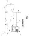
- FIG. 2is a generic circuit schematic of a direct current (DC) voltage converter 20 adapted to provide a regulated low voltage output (RLVO) as well as an auxiliary high voltage output (AHVO) in accordance with a preferred embodiment of the present invention.
- the voltage converter 20 in FIG. 2integrates a conventional step-down switching voltage regulator circuit with a multi-stage charge pump circuit in a novel manner to provide an auxiliary high voltage output (AHVO) without a dedicated integrated circuit for the charge pump.
- AHVOauxiliary high voltage output
- FIG. 2illustrates the voltage converter 20 , which includes a circuit block 12 that is coupled to an input terminal 13 that receives an applied input voltage V IN .
- the circuit block 12has an output stage that includes a pair of switches S 1 and S 2 connected in series between the input terminal 13 and ground. In the interest of clarity, only the output stage of the circuit block 12 is shown.
- the specific details of an implementation of control circuitry 15 for driving the switches S 1 and S 2 to their respective “ON” and “OFF” stateshas been omitted. It will of course be appreciated that in the development of any implementation of the control circuitry 15 , numerous implementation-specific decisions must be made to achieve the developer's specific goals, such as compliance with system-related and business-related constraints, which will vary from one implementation to another. Moreover, it will be understood that such a development effort might be complex and time-consuming, but would nevertheless be a routine undertaking for those of ordinary skill in the art having the benefit of this disclosure.
- An output LC filterthat includes an inductor L 1 and a capacitor C 3 is connected at a junction 23 between the pair of switches S 1 and S 2 .
- the regulated low voltage output (RLVO)is provided at an output terminal 27 of the LC filter.
- a feedback path 14is provided from the output of the LC filter to the control circuitry 15 of circuit block 12 in order to appropriately control the turning “ON” and “OFF” of the switches S 1 and S 2 .
- the input terminal 13is also connected via a first diode D 1 to a node 26 which, in turn, is connected to one electrode of a first capacitor C 1 .
- the orientation of the first diode D 1is such that its anode is connected to the input terminal 13 while its cathode is connected to the node 26 .
- the other electrode of the first capacitor C 1is connected to the junction 23 between the pair of switches S 1 and S 2 .
- the first diode D 1 and first capacitor C 2form a first stage of the multi-stage charge pump add-on circuit of the power supply 20 .
- the junction between the first diode D 1 and the first capacitor C 1 at node 26is connected via a second diode D 2 to an output terminal 28 , which provides an auxiliary high voltage output (AHVO).
- the orientation of the second diode D 2is such that its anode is connected to node 26 while its cathode is connected to the output terminal 28 .
- the output terminal 28is further connected via a second capacitor C 2 to ground.
- the “push-pull” output stage of the circuit block 12switches between the applied input voltage V IN and 0 volts at a frequency defined by the particular device application.
- a controller(not shown) drives the switches to connect the output filter to the applied input voltage V IN or to ground to maintain the output voltage at a predetermined level. Specifically, the controller drives the switches S 1 and S 2 so as to connect and disconnect the applied input voltage V IN to the output filter to generate the regulated low voltage output (RLVO).
- the applied input voltage V INis taken to be +3.3 V for the remainder of the disclosure although it will be understood that any input voltage could be used.
- the output of the circuit block 12switches between the applied input voltage V IN ( ⁇ +3.3 V) and 0 volts to provide a regulated low voltage output (RLVO) at the output terminal 27 .
- RLVOregulated low voltage output
- the output of the circuit block 12switches to 0 V (i.e. when the voltage switch S 1 is turned “OFF” and the switch S 2 is turned “ON”), the first diode D 1 is forward biased resulting in the first capacitor C 1 being charged to +3.3 V minus a forward voltage drop (V D ) across the first diode D 1 .
- the forward voltage drop (V D )is typically 0.2 V for a Schottky device or, alternatively, 0.7 V for a normal diode. Assuming Schottky diode operation, the first capacitor C 1 is charged to (3.3-0.2) V or 3.1 V.
- the voltage V x at node 26rises momentarily to +6.4 V (3.3 V+3.1 V) and the first diode D 1 is reverse biased.
- the first capacitor C 1thereby discharges into the second capacitor C 2 via forward-biasing of the second diode D 2 .
- the resulting voltage across the second capacitor C 2will be the auxiliary high voltage output (AHVO). Specifically, this voltage will be 6.4 V minus the forward voltage drop (V D ) across the second diode D 2 (i.e. 0.2 V for a Schottky device or 0.7 V for a normal diode).
- AHVOauxiliary high voltage output
- the present inventionuses the inherent properties of a conventional step-down switching voltage regulator with a push-pull output stage to provide an auxiliary voltage rail higher than the input supply voltage.
- the push-pull output stage of the step-down voltage regulatoris used to drive a charge pump voltage-doubler circuit.
- the circuit topology of the present inventionprovides a low component count (i.e. two diodes and two capacitors) resulting in lower component cost and smaller physical size.
- switches S 1 and S 2 in FIG. 2may be any suitable switch type for connecting and disconnecting the applied input voltage V IN to the output terminal 23 of the circuit block 12 .
- transistor switchesmay be used in which case any of bipolar junction transistor (BJT), junction field-effect transistor (JFET), metal oxide semiconductor field effect transistors (MOSFET), or bipolar CMOS (BiCMOS) technologies may be employed.
- BJTbipolar junction transistor
- JFETjunction field-effect transistor
- MOSFETmetal oxide semiconductor field effect transistors
- BiCMOSbipolar CMOS
- the multi-stage charge pump circuitry depicted in FIG. 2may include additional diode-capacitor stages cascaded together in order to boost the input voltage to higher levels.
- the voltage converter of the present inventionmay be adapted to provide an auxiliary high voltage output (AHVO) equal to n(V IN ⁇ V D ), where n equals the number of diode-capacitor stages in the multi-stage charge pump circuitry.
- AHVOauxiliary high voltage output
Landscapes
- Engineering & Computer Science (AREA)
- Power Engineering (AREA)
- Dc-Dc Converters (AREA)
Abstract
Description
Claims (16)
Priority Applications (1)
| Application Number | Priority Date | Filing Date | Title |
|---|---|---|---|
| US10/189,548US6756772B2 (en) | 2002-07-08 | 2002-07-08 | Dual-output direct current voltage converter |
Applications Claiming Priority (1)
| Application Number | Priority Date | Filing Date | Title |
|---|---|---|---|
| US10/189,548US6756772B2 (en) | 2002-07-08 | 2002-07-08 | Dual-output direct current voltage converter |
Publications (2)
| Publication Number | Publication Date |
|---|---|
| US20040004465A1 US20040004465A1 (en) | 2004-01-08 |
| US6756772B2true US6756772B2 (en) | 2004-06-29 |
Family
ID=29999672
Family Applications (1)
| Application Number | Title | Priority Date | Filing Date |
|---|---|---|---|
| US10/189,548Expired - Fee RelatedUS6756772B2 (en) | 2002-07-08 | 2002-07-08 | Dual-output direct current voltage converter |
Country Status (1)
| Country | Link |
|---|---|
| US (1) | US6756772B2 (en) |
Cited By (51)
| Publication number | Priority date | Publication date | Assignee | Title |
|---|---|---|---|---|
| US20030035260A1 (en)* | 2001-08-16 | 2003-02-20 | Intersil Americas Inc. | Integrated circuit for generating a plurality of direct current (DC) output voltages |
| US20050219865A1 (en)* | 2004-03-30 | 2005-10-06 | Vogman Viktor D | Voltage regulator current sensing |
| US20070008754A1 (en)* | 2005-07-06 | 2007-01-11 | Electro Scientific Industries, Inc. | Charge pump for bus-powered device |
| US20070097719A1 (en)* | 2005-11-03 | 2007-05-03 | Jordi Parramon | Cascaded step-up converter and charge pump for efficient compliance voltage generation in an implantable stimulator device |
| US20080013345A1 (en)* | 2006-07-14 | 2008-01-17 | Mitsumi Electric Co. Ltd. | DC-DC converter and power supply apparatus |
| US20090027928A1 (en)* | 2007-07-28 | 2009-01-29 | Xiaopeng Dong | Step up converter with overcurrent protection |
| WO2009075547A3 (en)* | 2007-12-13 | 2009-09-03 | Ad Tech Co., Ltd. | Power supply for multiple output voltages |
| US20100013548A1 (en)* | 2008-07-18 | 2010-01-21 | Analog Devices, Inc. | Power efficient charge pump with controlled peak currents |
| US20100020579A1 (en)* | 2008-07-25 | 2010-01-28 | Melanson John L | Power Supply With Accurate Energy Measurement |
| US20100060202A1 (en)* | 2007-03-12 | 2010-03-11 | Melanson John L | Lighting System with Lighting Dimmer Output Mapping |
| US20100156319A1 (en)* | 2008-08-29 | 2010-06-24 | John Laurence Melanson | LED Lighting System with Accurate Current Control |
| US20100164631A1 (en)* | 2008-12-31 | 2010-07-01 | Cirrus Logic, Inc. | Electronic system having common mode voltage range enhancement |
| US20100171442A1 (en)* | 2008-12-12 | 2010-07-08 | Draper William A | Light Emitting Diode Based Lighting System With Time Division Ambient Light Feedback Response |
| US20100244726A1 (en)* | 2008-12-07 | 2010-09-30 | Melanson John L | Primary-side based control of secondary-side current for a transformer |
| US20100253305A1 (en)* | 2007-03-12 | 2010-10-07 | Melanson John L | Switching power converter control with spread spectrum based electromagnetic interference reduction |
| US20100308742A1 (en)* | 2007-03-12 | 2010-12-09 | Melanson John L | Power Control System for Current Regulated Light Sources |
| US7969125B2 (en) | 2007-05-02 | 2011-06-28 | Cirrus Logic, Inc. | Programmable power control system |
| US20110204724A1 (en)* | 2010-02-22 | 2011-08-25 | Ashutosh Verma | Dual Output Direct Current (DC)-DC Regulator |
| WO2011103058A1 (en)* | 2010-02-22 | 2011-08-25 | Marvell World Trade Ltd | Dual output direct current (dc)-dc regulator |
| US20110204863A1 (en)* | 2010-02-19 | 2011-08-25 | Spencer John R | Power Regulator System and Method |
| US20110210674A1 (en)* | 2007-08-24 | 2011-09-01 | Cirrus Logic, Inc. | Multi-LED Control |
| US8018171B1 (en) | 2007-03-12 | 2011-09-13 | Cirrus Logic, Inc. | Multi-function duty cycle modifier |
| US8022683B2 (en) | 2008-01-30 | 2011-09-20 | Cirrus Logic, Inc. | Powering a power supply integrated circuit with sense current |
| US8076920B1 (en) | 2007-03-12 | 2011-12-13 | Cirrus Logic, Inc. | Switching power converter and control system |
| US8102127B2 (en) | 2007-06-24 | 2012-01-24 | Cirrus Logic, Inc. | Hybrid gas discharge lamp-LED lighting system |
| US8179110B2 (en) | 2008-09-30 | 2012-05-15 | Cirrus Logic Inc. | Adjustable constant current source with continuous conduction mode (“CCM”) and discontinuous conduction mode (“DCM”) operation |
| US20120153916A1 (en)* | 2010-12-21 | 2012-06-21 | Exar Corporation | Digital boost feedback voltage controller for switch-mode power supplies using pulse-frequency modulation |
| US8212491B2 (en) | 2008-07-25 | 2012-07-03 | Cirrus Logic, Inc. | Switching power converter control with triac-based leading edge dimmer compatibility |
| US8248145B2 (en) | 2009-06-30 | 2012-08-21 | Cirrus Logic, Inc. | Cascode configured switching using at least one low breakdown voltage internal, integrated circuit switch to control at least one high breakdown voltage external switch |
| US8299722B2 (en) | 2008-12-12 | 2012-10-30 | Cirrus Logic, Inc. | Time division light output sensing and brightness adjustment for different spectra of light emitting diodes |
| US8344707B2 (en) | 2008-07-25 | 2013-01-01 | Cirrus Logic, Inc. | Current sensing in a switching power converter |
| US8482223B2 (en) | 2009-04-30 | 2013-07-09 | Cirrus Logic, Inc. | Calibration of lamps |
| US8536799B1 (en) | 2010-07-30 | 2013-09-17 | Cirrus Logic, Inc. | Dimmer detection |
| US8569972B2 (en) | 2010-08-17 | 2013-10-29 | Cirrus Logic, Inc. | Dimmer output emulation |
| US8576589B2 (en) | 2008-01-30 | 2013-11-05 | Cirrus Logic, Inc. | Switch state controller with a sense current generated operating voltage |
| CN103457460A (en)* | 2013-08-26 | 2013-12-18 | 华南理工大学 | High-gain boost converter based on coupling inductance and voltage transfer technology |
| US8654483B2 (en) | 2009-11-09 | 2014-02-18 | Cirrus Logic, Inc. | Power system having voltage-based monitoring for over current protection |
| US8729811B2 (en) | 2010-07-30 | 2014-05-20 | Cirrus Logic, Inc. | Dimming multiple lighting devices by alternating energy transfer from a magnetic storage element |
| US8823289B2 (en) | 2011-03-24 | 2014-09-02 | Cirrus Logic, Inc. | Color coordination of electronic light sources with dimming and temperature responsiveness |
| US8912734B2 (en) | 2011-03-24 | 2014-12-16 | Cirrus Logic, Inc. | Color mixing of electronic light sources with correlation between phase-cut dimmer angle and predetermined black body radiation function |
| US8963535B1 (en) | 2009-06-30 | 2015-02-24 | Cirrus Logic, Inc. | Switch controlled current sensing using a hall effect sensor |
| US9155174B2 (en) | 2009-09-30 | 2015-10-06 | Cirrus Logic, Inc. | Phase control dimming compatible lighting systems |
| US9173261B2 (en) | 2010-07-30 | 2015-10-27 | Wesley L. Mokry | Secondary-side alternating energy transfer control with inverted reference and LED-derived power supply |
| US9178415B1 (en) | 2009-10-15 | 2015-11-03 | Cirrus Logic, Inc. | Inductor over-current protection using a volt-second value representing an input voltage to a switching power converter |
| US9204503B1 (en) | 2012-07-03 | 2015-12-01 | Philips International, B.V. | Systems and methods for dimming multiple lighting devices by alternating transfer from a magnetic storage element |
| US10063147B2 (en) | 2014-10-02 | 2018-08-28 | Infineon Technologies Austria Ag | Multiple output boost DC-DC power converter |
| US10247893B1 (en)* | 2017-11-21 | 2019-04-02 | Corning Optical Communications Wireless Ltd | Optical connector assemblies and optical cable assemblies with supplemental input voltage |
| US10284155B2 (en) | 2014-12-30 | 2019-05-07 | Infineon Technologies Austria Ag | Multi-level class D audio power amplifiers |
| WO2020000703A1 (en)* | 2018-06-29 | 2020-01-02 | 深圳市华星光电半导体显示技术有限公司 | Voltage generation circuit |
| US11121625B2 (en) | 2017-08-14 | 2021-09-14 | Interdigital Madison Patent Holdings, Sas | Voltage doubler using a switching regulator and voltage limiter |
| US12383745B2 (en) | 2019-09-06 | 2025-08-12 | Boston Scientific Neuromodulation Corporation | Management of compliance voltage for a stimulator device |
Families Citing this family (10)
| Publication number | Priority date | Publication date | Assignee | Title |
|---|---|---|---|---|
| DE102005020314A1 (en)* | 2005-05-02 | 2006-11-09 | Infineon Technologies Ag | A power supply arrangement for supplying a first electrical load and method for providing an electrical power |
| JP4787114B2 (en)* | 2006-09-26 | 2011-10-05 | 株式会社リコー | Real-time clock device, semiconductor device using the real-time clock device, and electronic equipment |
| US8008898B2 (en)* | 2008-01-30 | 2011-08-30 | Cirrus Logic, Inc. | Switching regulator with boosted auxiliary winding supply |
| US8008902B2 (en)* | 2008-06-25 | 2011-08-30 | Cirrus Logic, Inc. | Hysteretic buck converter having dynamic thresholds |
| US8222872B1 (en) | 2008-09-30 | 2012-07-17 | Cirrus Logic, Inc. | Switching power converter with selectable mode auxiliary power supply |
| US8212493B2 (en) | 2009-06-30 | 2012-07-03 | Cirrus Logic, Inc. | Low energy transfer mode for auxiliary power supply operation in a cascaded switching power converter |
| US8198874B2 (en) | 2009-06-30 | 2012-06-12 | Cirrus Logic, Inc. | Switching power converter with current sensing transformer auxiliary power supply |
| CN107040134A (en)* | 2017-05-05 | 2017-08-11 | 广东工业大学 | A kind of dual output DC transfer circuit |
| CN110071636B (en)* | 2019-05-30 | 2021-07-06 | 广东工业大学 | A DC conversion circuit |
| CN113689813A (en)* | 2021-08-16 | 2021-11-23 | Tcl华星光电技术有限公司 | Drive circuit and display device |
Citations (11)
| Publication number | Priority date | Publication date | Assignee | Title |
|---|---|---|---|---|
| US5245524A (en) | 1990-10-31 | 1993-09-14 | Fujitsu Limited | DC-DC converter of charge pump type |
| US5336985A (en)* | 1992-11-09 | 1994-08-09 | Compaq Computer Corp. | Tapped inductor slave regulating circuit |
| US5412308A (en)* | 1994-01-06 | 1995-05-02 | Hewlett-Packard Corporation | Dual voltage power supply |
| US5455501A (en)* | 1994-03-24 | 1995-10-03 | Intel Corporation | Multiple output DC-DC converter with different ranges of output assurance and capable of tolerating load transients |
| US5532577A (en)* | 1994-04-01 | 1996-07-02 | Maxim Integrated Products, Inc. | Method and apparatus for multiple output regulation in a step-down switching regulator |
| US5635776A (en) | 1992-02-27 | 1997-06-03 | Texas Instruments Incorporated | Charge pump voltage converter |
| US5886508A (en)* | 1997-08-29 | 1999-03-23 | Computer Products, Inc. | Multiple output voltages from a cascaded buck converter topology |
| US5959442A (en) | 1997-09-30 | 1999-09-28 | Intel Corporation | Buck converter |
| US6222352B1 (en)* | 1999-05-06 | 2001-04-24 | Fairchild Semiconductor Corporation | Multiple voltage output buck converter with a single inductor |
| US6479972B1 (en)* | 2000-09-11 | 2002-11-12 | Elite Semiconductor Memory Technology Inc. | Voltage regulator for supplying power to internal circuits |
| US6566846B1 (en)* | 2000-11-10 | 2003-05-20 | Marvell International, Ltd | Cascode regulator with plural outputs |
Family Cites Families (12)
| Publication number | Priority date | Publication date | Assignee | Title |
|---|---|---|---|---|
| US5347525A (en)* | 1993-02-19 | 1994-09-13 | Sri International | Generation of multiple stabilized frequency references using a mode-coupled laser |
| US5396506A (en)* | 1993-12-09 | 1995-03-07 | United Technologies Corporation | Coupled multiple output fiber laser |
| US5477368A (en)* | 1994-12-29 | 1995-12-19 | At&T Corp. | High power lightwave transmitter using highly saturated amplifier for residual AM suppression |
| US5566381A (en)* | 1995-03-02 | 1996-10-15 | Lucent Technologies Inc. | Multifrequency lightwave source using phase modulation for suppressing stimulated brillouin scattering in optical fibers |
| US5694408A (en)* | 1995-06-07 | 1997-12-02 | Mcdonnell Douglas Corporation | Fiber optic laser system and associated lasing method |
| US6058128A (en)* | 1996-03-25 | 2000-05-02 | Sdl, Inc. | Apparatus for providing a stabilized laser source |
| US6215809B1 (en)* | 1996-03-25 | 2001-04-10 | Sdl, Inc. | Stabilization of laser sources with closely-coupled optical reflectors using an internal dither circuit |
| US6072614A (en)* | 1997-08-21 | 2000-06-06 | Nortel Networks Corporation | Monitoring induced counterpropagating signals in optical communications systems |
| US6061170A (en)* | 1998-03-16 | 2000-05-09 | Mcdonnell Douglas Corporation | Dual frequency laser amplifier array and operating method therefor |
| US6496297B1 (en)* | 2000-12-22 | 2002-12-17 | Ciena Corporation | Device and method for modulating an optical signal |
| US20030002138A1 (en)* | 2001-06-27 | 2003-01-02 | International Business Machines Corporation | Gain stabilized raman effect optical amplifiers for coarse and dense wavelength multiplexers |
| US20030123133A1 (en)* | 2001-07-25 | 2003-07-03 | Damian Flannery | Distributed raman amplifier module auto-setup |
- 2002
- 2002-07-08USUS10/189,548patent/US6756772B2/ennot_activeExpired - Fee Related
Patent Citations (11)
| Publication number | Priority date | Publication date | Assignee | Title |
|---|---|---|---|---|
| US5245524A (en) | 1990-10-31 | 1993-09-14 | Fujitsu Limited | DC-DC converter of charge pump type |
| US5635776A (en) | 1992-02-27 | 1997-06-03 | Texas Instruments Incorporated | Charge pump voltage converter |
| US5336985A (en)* | 1992-11-09 | 1994-08-09 | Compaq Computer Corp. | Tapped inductor slave regulating circuit |
| US5412308A (en)* | 1994-01-06 | 1995-05-02 | Hewlett-Packard Corporation | Dual voltage power supply |
| US5455501A (en)* | 1994-03-24 | 1995-10-03 | Intel Corporation | Multiple output DC-DC converter with different ranges of output assurance and capable of tolerating load transients |
| US5532577A (en)* | 1994-04-01 | 1996-07-02 | Maxim Integrated Products, Inc. | Method and apparatus for multiple output regulation in a step-down switching regulator |
| US5886508A (en)* | 1997-08-29 | 1999-03-23 | Computer Products, Inc. | Multiple output voltages from a cascaded buck converter topology |
| US5959442A (en) | 1997-09-30 | 1999-09-28 | Intel Corporation | Buck converter |
| US6222352B1 (en)* | 1999-05-06 | 2001-04-24 | Fairchild Semiconductor Corporation | Multiple voltage output buck converter with a single inductor |
| US6479972B1 (en)* | 2000-09-11 | 2002-11-12 | Elite Semiconductor Memory Technology Inc. | Voltage regulator for supplying power to internal circuits |
| US6566846B1 (en)* | 2000-11-10 | 2003-05-20 | Marvell International, Ltd | Cascode regulator with plural outputs |
Non-Patent Citations (3)
| Title |
|---|
| Article "Simple Design of Low-Ripple DC/DC Boost Converter", Nikkei Electronics Asia, Dec. 2000. |
| Article DC-DC Converter Tutorial, 2002, Maxim Integrated Products. |
| Website Info "Switch Mode Power Supply", Power Designers, pp. 1-5 and 1-11. |
Cited By (79)
| Publication number | Priority date | Publication date | Assignee | Title |
|---|---|---|---|---|
| US7023187B2 (en)* | 2001-08-16 | 2006-04-04 | Intersil Americas Inc. | Integrated circuit for generating a plurality of direct current (DC) output voltages |
| US20030035260A1 (en)* | 2001-08-16 | 2003-02-20 | Intersil Americas Inc. | Integrated circuit for generating a plurality of direct current (DC) output voltages |
| US20050219865A1 (en)* | 2004-03-30 | 2005-10-06 | Vogman Viktor D | Voltage regulator current sensing |
| US7064530B2 (en)* | 2004-03-30 | 2006-06-20 | Intel Corporation | Voltage regulator current sensing |
| US7656427B2 (en) | 2005-07-06 | 2010-02-02 | Electro Scientific Industries, Inc. | Charge pump for bus-powered device |
| US20070008754A1 (en)* | 2005-07-06 | 2007-01-11 | Electro Scientific Industries, Inc. | Charge pump for bus-powered device |
| WO2007008449A1 (en)* | 2005-07-06 | 2007-01-18 | Electro Scientific Industries, Inc. | Charge pump for bus-powered device |
| US20080238198A1 (en)* | 2005-07-06 | 2008-10-02 | Electro Scientific Industries, Inc. | Charge pump for bus-powered device |
| US20070097719A1 (en)* | 2005-11-03 | 2007-05-03 | Jordi Parramon | Cascaded step-up converter and charge pump for efficient compliance voltage generation in an implantable stimulator device |
| US7872884B2 (en)* | 2005-11-03 | 2011-01-18 | Boston Scientific Neuromodulation Corporation | Cascaded step-up converter and charge pump for efficient compliance voltage generation in an implantable stimulator device |
| US20080013345A1 (en)* | 2006-07-14 | 2008-01-17 | Mitsumi Electric Co. Ltd. | DC-DC converter and power supply apparatus |
| US7782028B2 (en)* | 2006-07-14 | 2010-08-24 | Mitsumi Electric Co., Ltd. | DC-DC converter and power supply apparatus |
| US8018171B1 (en) | 2007-03-12 | 2011-09-13 | Cirrus Logic, Inc. | Multi-function duty cycle modifier |
| US8536794B2 (en) | 2007-03-12 | 2013-09-17 | Cirrus Logic, Inc. | Lighting system with lighting dimmer output mapping |
| US20100060202A1 (en)* | 2007-03-12 | 2010-03-11 | Melanson John L | Lighting System with Lighting Dimmer Output Mapping |
| US8232736B2 (en) | 2007-03-12 | 2012-07-31 | Cirrus Logic, Inc. | Power control system for current regulated light sources |
| US8174204B2 (en) | 2007-03-12 | 2012-05-08 | Cirrus Logic, Inc. | Lighting system with power factor correction control data determined from a phase modulated signal |
| US8723438B2 (en) | 2007-03-12 | 2014-05-13 | Cirrus Logic, Inc. | Switch power converter control with spread spectrum based electromagnetic interference reduction |
| US20100253305A1 (en)* | 2007-03-12 | 2010-10-07 | Melanson John L | Switching power converter control with spread spectrum based electromagnetic interference reduction |
| US8076920B1 (en) | 2007-03-12 | 2011-12-13 | Cirrus Logic, Inc. | Switching power converter and control system |
| US20100308742A1 (en)* | 2007-03-12 | 2010-12-09 | Melanson John L | Power Control System for Current Regulated Light Sources |
| US8125805B1 (en) | 2007-05-02 | 2012-02-28 | Cirrus Logic Inc. | Switch-mode converter operating in a hybrid discontinuous conduction mode (DCM)/continuous conduction mode (CCM) that uses double or more pulses in a switching period |
| US8120341B2 (en) | 2007-05-02 | 2012-02-21 | Cirrus Logic, Inc. | Switching power converter with switch control pulse width variability at low power demand levels |
| US8040703B2 (en) | 2007-05-02 | 2011-10-18 | Cirrus Logic, Inc. | Power factor correction controller with feedback reduction |
| US7969125B2 (en) | 2007-05-02 | 2011-06-28 | Cirrus Logic, Inc. | Programmable power control system |
| US8102127B2 (en) | 2007-06-24 | 2012-01-24 | Cirrus Logic, Inc. | Hybrid gas discharge lamp-LED lighting system |
| US8816588B2 (en) | 2007-06-24 | 2014-08-26 | Cirrus Logic, Inc. | Hybrid gas discharge lamp-LED lighting system |
| US20090027928A1 (en)* | 2007-07-28 | 2009-01-29 | Xiaopeng Dong | Step up converter with overcurrent protection |
| US20110210674A1 (en)* | 2007-08-24 | 2011-09-01 | Cirrus Logic, Inc. | Multi-LED Control |
| US8587217B2 (en) | 2007-08-24 | 2013-11-19 | Cirrus Logic, Inc. | Multi-LED control |
| CN101884159B (en)* | 2007-12-13 | 2013-07-31 | Ad技术有限公司 | Multiple Voltage Power Supply Unit |
| WO2009075547A3 (en)* | 2007-12-13 | 2009-09-03 | Ad Tech Co., Ltd. | Power supply for multiple output voltages |
| CN101884159A (en)* | 2007-12-13 | 2010-11-10 | Ad技术有限公司 | Multiple-voltage power supply apparatus |
| US8576589B2 (en) | 2008-01-30 | 2013-11-05 | Cirrus Logic, Inc. | Switch state controller with a sense current generated operating voltage |
| US8022683B2 (en) | 2008-01-30 | 2011-09-20 | Cirrus Logic, Inc. | Powering a power supply integrated circuit with sense current |
| US20100013548A1 (en)* | 2008-07-18 | 2010-01-21 | Analog Devices, Inc. | Power efficient charge pump with controlled peak currents |
| US8330434B2 (en) | 2008-07-25 | 2012-12-11 | Cirrus Logic, Inc. | Power supply that determines energy consumption and outputs a signal indicative of energy consumption |
| US20100020579A1 (en)* | 2008-07-25 | 2010-01-28 | Melanson John L | Power Supply With Accurate Energy Measurement |
| US8344707B2 (en) | 2008-07-25 | 2013-01-01 | Cirrus Logic, Inc. | Current sensing in a switching power converter |
| US8212491B2 (en) | 2008-07-25 | 2012-07-03 | Cirrus Logic, Inc. | Switching power converter control with triac-based leading edge dimmer compatibility |
| US8487546B2 (en) | 2008-08-29 | 2013-07-16 | Cirrus Logic, Inc. | LED lighting system with accurate current control |
| US20100156319A1 (en)* | 2008-08-29 | 2010-06-24 | John Laurence Melanson | LED Lighting System with Accurate Current Control |
| US8179110B2 (en) | 2008-09-30 | 2012-05-15 | Cirrus Logic Inc. | Adjustable constant current source with continuous conduction mode (“CCM”) and discontinuous conduction mode (“DCM”) operation |
| US8288954B2 (en) | 2008-12-07 | 2012-10-16 | Cirrus Logic, Inc. | Primary-side based control of secondary-side current for a transformer |
| US20100244726A1 (en)* | 2008-12-07 | 2010-09-30 | Melanson John L | Primary-side based control of secondary-side current for a transformer |
| US8299722B2 (en) | 2008-12-12 | 2012-10-30 | Cirrus Logic, Inc. | Time division light output sensing and brightness adjustment for different spectra of light emitting diodes |
| US8362707B2 (en) | 2008-12-12 | 2013-01-29 | Cirrus Logic, Inc. | Light emitting diode based lighting system with time division ambient light feedback response |
| US20100171442A1 (en)* | 2008-12-12 | 2010-07-08 | Draper William A | Light Emitting Diode Based Lighting System With Time Division Ambient Light Feedback Response |
| US20100164631A1 (en)* | 2008-12-31 | 2010-07-01 | Cirrus Logic, Inc. | Electronic system having common mode voltage range enhancement |
| US7994863B2 (en) | 2008-12-31 | 2011-08-09 | Cirrus Logic, Inc. | Electronic system having common mode voltage range enhancement |
| US8482223B2 (en) | 2009-04-30 | 2013-07-09 | Cirrus Logic, Inc. | Calibration of lamps |
| US8963535B1 (en) | 2009-06-30 | 2015-02-24 | Cirrus Logic, Inc. | Switch controlled current sensing using a hall effect sensor |
| US8248145B2 (en) | 2009-06-30 | 2012-08-21 | Cirrus Logic, Inc. | Cascode configured switching using at least one low breakdown voltage internal, integrated circuit switch to control at least one high breakdown voltage external switch |
| US9155174B2 (en) | 2009-09-30 | 2015-10-06 | Cirrus Logic, Inc. | Phase control dimming compatible lighting systems |
| US9178415B1 (en) | 2009-10-15 | 2015-11-03 | Cirrus Logic, Inc. | Inductor over-current protection using a volt-second value representing an input voltage to a switching power converter |
| US8654483B2 (en) | 2009-11-09 | 2014-02-18 | Cirrus Logic, Inc. | Power system having voltage-based monitoring for over current protection |
| US20110204863A1 (en)* | 2010-02-19 | 2011-08-25 | Spencer John R | Power Regulator System and Method |
| US9350234B2 (en) | 2010-02-22 | 2016-05-24 | Marvell World Trade Ltd. | Voltage regulator and method for regulating dual output voltages by selective connection between a voltage supply and multiple capacitances |
| US8582332B2 (en) | 2010-02-22 | 2013-11-12 | Marvell World Trade Ltd. | Dual output DC-DC charge pump regulator |
| US20110204724A1 (en)* | 2010-02-22 | 2011-08-25 | Ashutosh Verma | Dual Output Direct Current (DC)-DC Regulator |
| WO2011103058A1 (en)* | 2010-02-22 | 2011-08-25 | Marvell World Trade Ltd | Dual output direct current (dc)-dc regulator |
| US9173261B2 (en) | 2010-07-30 | 2015-10-27 | Wesley L. Mokry | Secondary-side alternating energy transfer control with inverted reference and LED-derived power supply |
| US8729811B2 (en) | 2010-07-30 | 2014-05-20 | Cirrus Logic, Inc. | Dimming multiple lighting devices by alternating energy transfer from a magnetic storage element |
| US8536799B1 (en) | 2010-07-30 | 2013-09-17 | Cirrus Logic, Inc. | Dimmer detection |
| US8569972B2 (en) | 2010-08-17 | 2013-10-29 | Cirrus Logic, Inc. | Dimmer output emulation |
| US20120153916A1 (en)* | 2010-12-21 | 2012-06-21 | Exar Corporation | Digital boost feedback voltage controller for switch-mode power supplies using pulse-frequency modulation |
| US8362756B2 (en)* | 2010-12-21 | 2013-01-29 | Exar Corporation | Digital boost feedback voltage controller for switch-mode power supplies using pulse-frequency modulation |
| US8823289B2 (en) | 2011-03-24 | 2014-09-02 | Cirrus Logic, Inc. | Color coordination of electronic light sources with dimming and temperature responsiveness |
| US8912734B2 (en) | 2011-03-24 | 2014-12-16 | Cirrus Logic, Inc. | Color mixing of electronic light sources with correlation between phase-cut dimmer angle and predetermined black body radiation function |
| US9204503B1 (en) | 2012-07-03 | 2015-12-01 | Philips International, B.V. | Systems and methods for dimming multiple lighting devices by alternating transfer from a magnetic storage element |
| CN103457460A (en)* | 2013-08-26 | 2013-12-18 | 华南理工大学 | High-gain boost converter based on coupling inductance and voltage transfer technology |
| US10063147B2 (en) | 2014-10-02 | 2018-08-28 | Infineon Technologies Austria Ag | Multiple output boost DC-DC power converter |
| US10284155B2 (en) | 2014-12-30 | 2019-05-07 | Infineon Technologies Austria Ag | Multi-level class D audio power amplifiers |
| US10985717B2 (en) | 2014-12-30 | 2021-04-20 | Infineon Technologies Austria Ag | Multi-level class D audio power amplifiers |
| US11121625B2 (en) | 2017-08-14 | 2021-09-14 | Interdigital Madison Patent Holdings, Sas | Voltage doubler using a switching regulator and voltage limiter |
| US10247893B1 (en)* | 2017-11-21 | 2019-04-02 | Corning Optical Communications Wireless Ltd | Optical connector assemblies and optical cable assemblies with supplemental input voltage |
| WO2020000703A1 (en)* | 2018-06-29 | 2020-01-02 | 深圳市华星光电半导体显示技术有限公司 | Voltage generation circuit |
| US11056974B2 (en) | 2018-06-29 | 2021-07-06 | Shenzhen China Star Optoelectronics Semiconductor Display Technology Co., Ltd. | Voltage generation circuit |
| US12383745B2 (en) | 2019-09-06 | 2025-08-12 | Boston Scientific Neuromodulation Corporation | Management of compliance voltage for a stimulator device |
Also Published As
| Publication number | Publication date |
|---|---|
| US20040004465A1 (en) | 2004-01-08 |
Similar Documents
| Publication | Publication Date | Title |
|---|---|---|
| US6756772B2 (en) | Dual-output direct current voltage converter | |
| US11626800B2 (en) | Hybrid DC-DC power converter with small voltage conversion ratio | |
| US8488340B2 (en) | Power converter with boost-buck-buck configuration utilizing an intermediate power regulating circuit | |
| US6563726B1 (en) | Synchronous bridge rectifier | |
| JP5744138B2 (en) | Time division capacitor DC / DC converter with multiple outputs | |
| US7345894B2 (en) | Cascode switch power supply | |
| JP5401546B2 (en) | Boost DC / DC voltage converter with improved transient current capability | |
| CN100454737C (en) | Switching regulator, power supply circuit including the same, and auxiliary battery charging circuit | |
| JP4471978B2 (en) | Switching power supply control circuit, switching power supply device, and electronic equipment using the same | |
| JPH0956150A (en) | Switching power supply | |
| US10511223B2 (en) | Voltage regulator having boost and charge pump functionality | |
| EP1872453A2 (en) | Method and apparatus for providing uninterruptible power | |
| KR20130111645A (en) | Dc/dc voltage converter including up inductive switching pre-regulator and capacitive switching post-converter | |
| US11652407B2 (en) | Switching capacitor converter and driving circuit | |
| US7202643B2 (en) | High efficiency DC-to-DC synchronous buck converter | |
| US6288919B1 (en) | Single stage AC/DC converter high frequency AC distribution systems | |
| KR20030015133A (en) | Power supply | |
| GB2264404A (en) | Resonant power supply | |
| US6307359B1 (en) | DC-DC converter powered by doubled output voltage | |
| US6396724B1 (en) | Charge-pumped DC bias supply | |
| CN111164870B (en) | Voltage multiplier using switching regulator and voltage limiter | |
| JPH08140341A (en) | Micro power supply device using switching element | |
| CN109217671B (en) | Floating ground voltage-stabilizing power supply circuit | |
| US12003180B2 (en) | Power supply for driving synchronous rectification elements of SEPIC converter | |
| JP3003437B2 (en) | Voltage converter |
Legal Events
| Date | Code | Title | Description |
|---|---|---|---|
| AS | Assignment | Owner name:COGENCY SEMICONDUCTOR INC., CANADA Free format text:ASSIGNMENT OF ASSIGNORS INTEREST;ASSIGNOR:MCINNIS, DONALD MIKE;REEL/FRAME:013087/0419 Effective date:20020704 | |
| AS | Assignment | Owner name:INTELLON CORPORATION, FLORIDA Free format text:ASSIGNMENT OF ASSIGNORS INTEREST;ASSIGNOR:COGENCY SEMICONDUCTOR, INC.;REEL/FRAME:014375/0510 Effective date:20040128 | |
| FEPP | Fee payment procedure | Free format text:PAYOR NUMBER ASSIGNED (ORIGINAL EVENT CODE: ASPN); ENTITY STATUS OF PATENT OWNER: LARGE ENTITY Free format text:PAT HOLDER NO LONGER CLAIMS SMALL ENTITY STATUS, ENTITY STATUS SET TO UNDISCOUNTED (ORIGINAL EVENT CODE: STOL); ENTITY STATUS OF PATENT OWNER: LARGE ENTITY | |
| FPAY | Fee payment | Year of fee payment:4 | |
| REMI | Maintenance fee reminder mailed | ||
| AS | Assignment | Owner name:ATHEROS POWERLINE LLC,CALIFORNIA Free format text:MERGER;ASSIGNOR:INTELLON CORPORAITON;REEL/FRAME:024103/0834 Effective date:20091215 Owner name:ATHEROS COMMUNICATIONS, INC.,CALIFORNIA Free format text:ASSIGNMENT OF ASSIGNORS INTEREST;ASSIGNOR:ATHEROS POWERLINE LLC;REEL/FRAME:024103/0872 Effective date:20091215 Owner name:ATHEROS POWERLINE LLC,CALIFORNIA Free format text:MERGER;ASSIGNOR:INTELLON CORPORATION;REEL/FRAME:024103/0834 Effective date:20091215 Owner name:ATHEROS POWERLINE LLC, CALIFORNIA Free format text:MERGER;ASSIGNOR:INTELLON CORPORATION;REEL/FRAME:024103/0834 Effective date:20091215 Owner name:ATHEROS COMMUNICATIONS, INC., CALIFORNIA Free format text:ASSIGNMENT OF ASSIGNORS INTEREST;ASSIGNOR:ATHEROS POWERLINE LLC;REEL/FRAME:024103/0872 Effective date:20091215 | |
| AS | Assignment | Owner name:QUALCOMM ATHEROS, INC., CALIFORNIA Free format text:MERGER;ASSIGNOR:ATHEROS COMMUNICATIONS, INC.;REEL/FRAME:027301/0678 Effective date:20110524 | |
| FPAY | Fee payment | Year of fee payment:8 | |
| AS | Assignment | Owner name:QUALCOMM INCORPORATED, CALIFORNIA Free format text:ASSIGNMENT OF ASSIGNORS INTEREST;ASSIGNOR:QUALCOMM ATHEROS, INC.;REEL/FRAME:029555/0937 Effective date:20121022 | |
| REMI | Maintenance fee reminder mailed | ||
| LAPS | Lapse for failure to pay maintenance fees | ||
| STCH | Information on status: patent discontinuation | Free format text:PATENT EXPIRED DUE TO NONPAYMENT OF MAINTENANCE FEES UNDER 37 CFR 1.362 | |
| FP | Lapsed due to failure to pay maintenance fee | Effective date:20160629 |