US6756633B2 - Semiconductor memory array of floating gate memory cells with horizontally oriented floating gate edges - Google Patents
Semiconductor memory array of floating gate memory cells with horizontally oriented floating gate edgesDownload PDFInfo
- Publication number
- US6756633B2 US6756633B2US10/183,834US18383402AUS6756633B2US 6756633 B2US6756633 B2US 6756633B2US 18383402 AUS18383402 AUS 18383402AUS 6756633 B2US6756633 B2US 6756633B2
- Authority
- US
- United States
- Prior art keywords
- floating gate
- substrate
- insulated
- channel region
- array
- Prior art date
- Legal status (The legal status is an assumption and is not a legal conclusion. Google has not performed a legal analysis and makes no representation as to the accuracy of the status listed.)
- Expired - Lifetime
Links
- 238000007667floatingMethods0.000titleclaimsabstractdescription136
- 239000004065semiconductorSubstances0.000titleclaimsabstractdescription41
- 239000000758substrateSubstances0.000claimsabstractdescription120
- 238000002955isolationMethods0.000claimsdescription42
- 229910052751metalInorganic materials0.000claimsdescription38
- 239000002184metalSubstances0.000claimsdescription38
- 239000000463materialSubstances0.000claimsdescription27
- 239000004020conductorSubstances0.000claimsdescription24
- HQVNEWCFYHHQES-UHFFFAOYSA-Nsilicon nitrideChemical compoundN12[Si]34N5[Si]62N3[Si]51N64HQVNEWCFYHHQES-UHFFFAOYSA-N0.000claimsdescription20
- 239000011810insulating materialSubstances0.000claimsdescription18
- 229910052581Si3N4Inorganic materials0.000claimsdescription12
- 230000005689Fowler Nordheim tunnelingEffects0.000claimsdescription8
- 238000000034methodMethods0.000abstractdescription136
- 239000010410layerSubstances0.000description279
- 150000004767nitridesChemical class0.000description125
- 230000008569processEffects0.000description116
- 125000006850spacer groupChemical group0.000description68
- VYPSYNLAJGMNEJ-UHFFFAOYSA-NSilicium dioxideChemical compoundO=[Si]=OVYPSYNLAJGMNEJ-UHFFFAOYSA-N0.000description36
- 230000015572biosynthetic processEffects0.000description33
- XUIMIQQOPSSXEZ-UHFFFAOYSA-NSiliconChemical compound[Si]XUIMIQQOPSSXEZ-UHFFFAOYSA-N0.000description32
- 238000000151depositionMethods0.000description32
- 229910021420polycrystalline siliconInorganic materials0.000description23
- 229920005591polysiliconPolymers0.000description23
- 230000003647oxidationEffects0.000description20
- 238000007254oxidation reactionMethods0.000description20
- 229910052710siliconInorganic materials0.000description20
- 239000010703siliconSubstances0.000description20
- 230000008021depositionEffects0.000description19
- 238000005468ion implantationMethods0.000description19
- 230000008878couplingEffects0.000description16
- 238000010168coupling processMethods0.000description16
- 238000005859coupling reactionMethods0.000description16
- 230000000873masking effectEffects0.000description13
- 238000012545processingMethods0.000description12
- 150000002500ionsChemical class0.000description11
- PXHVJJICTQNCMI-UHFFFAOYSA-NNickelChemical compound[Ni]PXHVJJICTQNCMI-UHFFFAOYSA-N0.000description10
- 238000001465metallisationMethods0.000description10
- BASFCYQUMIYNBI-UHFFFAOYSA-NplatinumChemical compound[Pt]BASFCYQUMIYNBI-UHFFFAOYSA-N0.000description10
- NBIIXXVUZAFLBC-UHFFFAOYSA-NPhosphoric acidChemical compoundOP(O)(O)=ONBIIXXVUZAFLBC-UHFFFAOYSA-N0.000description8
- 238000005530etchingMethods0.000description8
- 230000005641tunnelingEffects0.000description8
- 230000000694effectsEffects0.000description7
- 229960001866silicon dioxideDrugs0.000description6
- 235000012239silicon dioxideNutrition0.000description6
- 239000000377silicon dioxideSubstances0.000description6
- WFKWXMTUELFFGS-UHFFFAOYSA-NtungstenChemical compound[W]WFKWXMTUELFFGS-UHFFFAOYSA-N0.000description6
- 229910052721tungstenInorganic materials0.000description6
- 239000010937tungstenSubstances0.000description6
- ZOKXTWBITQBERF-UHFFFAOYSA-NMolybdenumChemical compound[Mo]ZOKXTWBITQBERF-UHFFFAOYSA-N0.000description5
- RTAQQCXQSZGOHL-UHFFFAOYSA-NTitaniumChemical compound[Ti]RTAQQCXQSZGOHL-UHFFFAOYSA-N0.000description5
- 229910017052cobaltInorganic materials0.000description5
- 239000010941cobaltSubstances0.000description5
- GUTLYIVDDKVIGB-UHFFFAOYSA-Ncobalt atomChemical compound[Co]GUTLYIVDDKVIGB-UHFFFAOYSA-N0.000description5
- 238000013461designMethods0.000description5
- 229910052750molybdenumInorganic materials0.000description5
- 239000011733molybdenumSubstances0.000description5
- 229910052759nickelInorganic materials0.000description5
- 229910052697platinumInorganic materials0.000description5
- 229910052719titaniumInorganic materials0.000description5
- 239000010936titaniumSubstances0.000description5
- 229910000147aluminium phosphateInorganic materials0.000description4
- 239000003989dielectric materialSubstances0.000description4
- 238000002161passivationMethods0.000description4
- 238000005498polishingMethods0.000description4
- 230000002829reductive effectEffects0.000description4
- 238000003491arrayMethods0.000description3
- 230000008901benefitEffects0.000description3
- 239000005380borophosphosilicate glassSubstances0.000description3
- 238000005516engineering processMethods0.000description3
- 239000007943implantSubstances0.000description3
- 238000001459lithographyMethods0.000description3
- 238000004518low pressure chemical vapour depositionMethods0.000description3
- 238000004519manufacturing processMethods0.000description3
- 238000005457optimizationMethods0.000description3
- 229920002120photoresistant polymerPolymers0.000description3
- 239000011241protective layerSubstances0.000description3
- 229910021332silicideInorganic materials0.000description3
- FVBUAEGBCNSCDD-UHFFFAOYSA-Nsilicide(4-)Chemical compound[Si-4]FVBUAEGBCNSCDD-UHFFFAOYSA-N0.000description3
- 238000009751slip formingMethods0.000description3
- -12000 Å)Chemical class0.000description2
- BOTDANWDWHJENH-UHFFFAOYSA-NTetraethyl orthosilicateChemical compoundCCO[Si](OCC)(OCC)OCCBOTDANWDWHJENH-UHFFFAOYSA-N0.000description2
- 230000002411adverseEffects0.000description2
- 230000007423decreaseEffects0.000description2
- 238000011065in-situ storageMethods0.000description2
- 239000012212insulatorSubstances0.000description2
- 239000007769metal materialSubstances0.000description2
- 230000001590oxidative effectEffects0.000description2
- 238000005549size reductionMethods0.000description2
- 238000012876topographyMethods0.000description2
- IOVCWXUNBOPUCH-UHFFFAOYSA-MNitrite anionChemical compound[O-]N=OIOVCWXUNBOPUCH-UHFFFAOYSA-M0.000description1
- ATJFFYVFTNAWJD-UHFFFAOYSA-NTinChemical compound[Sn]ATJFFYVFTNAWJD-UHFFFAOYSA-N0.000description1
- 229910052782aluminiumInorganic materials0.000description1
- XAGFODPZIPBFFR-UHFFFAOYSA-NaluminiumChemical compound[Al]XAGFODPZIPBFFR-UHFFFAOYSA-N0.000description1
- 238000005229chemical vapour depositionMethods0.000description1
- 238000007796conventional methodMethods0.000description1
- 230000003247decreasing effectEffects0.000description1
- 230000006870functionEffects0.000description1
- 239000002784hot electronSubstances0.000description1
- 230000036039immunityEffects0.000description1
- 238000002347injectionMethods0.000description1
- 239000007924injectionSubstances0.000description1
- 239000012774insulation materialSubstances0.000description1
- 230000010354integrationEffects0.000description1
- 230000007246mechanismEffects0.000description1
- 238000000059patterningMethods0.000description1
- 230000002093peripheral effectEffects0.000description1
- 238000000206photolithographyMethods0.000description1
- 230000009467reductionEffects0.000description1
- 238000012552reviewMethods0.000description1
- 238000000926separation methodMethods0.000description1
- 239000002356single layerSubstances0.000description1
- 230000001629suppressionEffects0.000description1
- ATJFFYVFTNAWJD-BJUDXGSMSA-Ntin-118 atomChemical compound[118Sn]ATJFFYVFTNAWJD-BJUDXGSMSA-N0.000description1
Images


Classifications
- H—ELECTRICITY
- H10—SEMICONDUCTOR DEVICES; ELECTRIC SOLID-STATE DEVICES NOT OTHERWISE PROVIDED FOR
- H10B—ELECTRONIC MEMORY DEVICES
- H10B41/00—Electrically erasable-and-programmable ROM [EEPROM] devices comprising floating gates
- H10B41/20—Electrically erasable-and-programmable ROM [EEPROM] devices comprising floating gates characterised by three-dimensional arrangements, e.g. with cells on different height levels
- H10B41/23—Electrically erasable-and-programmable ROM [EEPROM] devices comprising floating gates characterised by three-dimensional arrangements, e.g. with cells on different height levels with source and drain on different levels, e.g. with sloping channels
- H—ELECTRICITY
- H10—SEMICONDUCTOR DEVICES; ELECTRIC SOLID-STATE DEVICES NOT OTHERWISE PROVIDED FOR
- H10B—ELECTRONIC MEMORY DEVICES
- H10B69/00—Erasable-and-programmable ROM [EPROM] devices not provided for in groups H10B41/00 - H10B63/00, e.g. ultraviolet erasable-and-programmable ROM [UVEPROM] devices
- H—ELECTRICITY
- H10—SEMICONDUCTOR DEVICES; ELECTRIC SOLID-STATE DEVICES NOT OTHERWISE PROVIDED FOR
- H10D—INORGANIC ELECTRIC SEMICONDUCTOR DEVICES
- H10D30/00—Field-effect transistors [FET]
- H10D30/60—Insulated-gate field-effect transistors [IGFET]
- H10D30/68—Floating-gate IGFETs
- H10D30/6891—Floating-gate IGFETs characterised by the shapes, relative sizes or dispositions of the floating gate electrode
Definitions
- the present inventionrelates to a self-aligned method of forming a semiconductor memory array of floating gate memory cells.
- the present inventionalso relates to a semiconductor memory array of floating gate memory cells of the foregoing type.
- Non-volatile semiconductor memory cells using a floating gate to store charges thereon and memory arrays of such non-volatile memory cells formed in a semiconductor substrateare well known in the art.
- floating gate memory cellshave been of the split gate type, or stacked gate type.
- Self-alignmentis well known in the art. Self-alignment refers to the act of processing one or more steps involving one or more materials such that the features are automatically aligned with respect to one another in that step processing. Accordingly, the present invention uses the technique of self-alignment to achieve the manufacturing of a semiconductor memory array of the floating gate memory cell type.
- FIG. 1illustrates a well known non-volatile memory cell design, which includes a floating gate 1 disposed over and insulated from a semiconductor substrate 2 having source and drain regions 3 / 4 .
- a control gate 5has a first portion that is disposed laterally adjacent to the floating gate 1 , and a second portion that is disposed vertically over and overlapping the floating gate 1 .
- the floating gate 1includes a relatively sharp edge 6 that extends upwardly toward the control gate second portion. The edge 6 extending toward the overlapping portion of the control gate 5 enhances Fowler-Nordheim tunneling used to erase the memory cell.
- control gate 5 and floating gate 1must be maintained so that the upwardly oriented pointed edges can be used for the erase function.
- This cell architectureimposes a scaling limit on the erase coupling ratio due to the finite overlap capacitance between the control gate 5 and the floating gate 1 .
- the present inventionsolves the above mentioned problems by providing a self aligned method of forming memory cells with reduced size, by minimizing the space needed for the bit-line connection and word-line transistor and eliminating the need for a vertical overlap between the control gate and floating gate, and a memory cell array formed thereby.
- the present inventionis an electrically programmable and erasable memory device that includes a substrate of semiconductor material of a first conductivity type, first and second spaced-apart regions formed in the substrate and having a second conductivity type with a channel region of the substrate defined therebetween, an electrically conductive floating gate disposed over and insulated from at least a portion of the channel region, wherein the floating gate includes a horizontally oriented edge extending from a lateral side of the floating gate, and an electrically conductive control gate having at least a portion thereof disposed laterally adjacent to and insulated from the horizontally oriented edge.
- and array of electrically programmable and erasable memory devicesincludes a substrate of semiconductor material of a first conductivity type, and spaced apart isolation regions formed on the substrate which are generally parallel to one another and extend in a first direction, with an active region between each pair of adjacent isolation regions.
- Each of the active regionsincludes a plurality of memory cells, where each of the memory cells includes first and second spaced-apart regions formed in the substrate having a second conductivity type with a channel region of the substrate defined therebetween, an electrically conductive floating gate disposed over and insulated from at least a portion of the channel region wherein the floating gate includes a horizontally oriented edge extending from a lateral side of the floating gate, and an electrically conductive control gate having at least a portion thereof disposed laterally adjacent to and insulated from the horizontally oriented edge.
- a method of forming a semiconductor memory cellincludes the steps of forming first and second spaced apart regions in a semiconductor substrate having a conductivity type different from that of the substrate, wherein a channel region of the substrate is defined between the first and second regions, forming a floating gate of electrically conductive material disposed over and insulated from at least a portion of the channel region, wherein the floating gate includes a horizontally oriented edge extending from a lateral side of the floating gate, and forming a control gate of electrically conductive material having at least a portion thereof disposed laterally adjacent to and insulated from the horizontally oriented edge.
- a method of forming an array of semiconductor memory cellsincludes the steps of forming spaced apart isolation regions on the substrate having a first conductivity type which are generally parallel to one another and extend in a first direction, with an active region between each pair of adjacent isolation regions, forming a plurality of spaced apart first and second regions in the semiconductor substrate having a second conductivity type, wherein a plurality of channel regions in the active regions of the substrate are defined each extending between one of the first regions and one of the second regions, forming a plurality of floating gates of electrically conductive material each disposed over and insulated from at least a portion of one of the channel regions, wherein each of the floating gates includes a horizontally oriented edge extending from a lateral side of the floating gate, and forming a plurality of electrically conductive control gates each having at least a portion thereof disposed laterally adjacent to and insulated from one of the horizontally oriented edges.
- a method of operating an electrically programmable and erasable memory devicehaving an electrically conductive floating gate disposed over and insulated from a substrate of semiconductor material, and an electrically conductive control gate having at least a portion thereof disposed laterally adjacent to the floating gate and insulated therefrom by an insulating material, includes the step of placing a voltage on the control gate that is sufficiently positive relative to a voltage of the floating gate to induce electrons on the floating gate to laterally tunnel from a horizontally oriented edge extending from a lateral side of the floating gate, through the insulating material, and onto the control gate via Fowler-Nordheim tunneling.
- a method of operating an electrically programmable and erasable non-volatile memory cell having a first and a second state, and including an electrically conductive floating gate disposed over and insulated from a substrate of semiconductor material, and an electrically conductive control gate having at least a portion thereof disposed laterally adjacent to the floating gateincludes the steps of establishing a first state of the memory cell by injecting electrons from a drain region of the substrate onto the floating gate, wherein the source region is disposed below a surface of the substrate and the injected electrons travel through the substrate in a direction generally perpendicular to the surface of the substrate, and establishing a second state of the memory cell by removing electrons from the floating gate to the control gate via Fowler-Nordheim tunneling through an insulating material disposed therebetween, wherein the removed electrons tunnel from a horizontally oriented edge extending from a lateral side of the floating gate, through the insulating material, and onto the control gate in a direction generally
- FIG. 1is a side cross-sectional view showing a conventional split-gate non-volatile memory cell.
- FIG. 2Ais a top view of a semiconductor substrate used in the first step of the method of present invention to form isolation regions.
- FIG. 2Bis a cross sectional view of the structure taken along the line 1 — 1 showing the initial processing steps of the present invention.
- FIG. 2Cis a top view of the structure showing the next step in the processing of the structure of FIG. 2B, in which isolation regions are formed.
- FIG. 2Dis a cross sectional view of the structure in FIG. 2C taken along the line 1 — 1 showing the isolation stripes formed in the structure.
- FIG. 2Eis a cross sectional view of the structure in FIG. 2C taken along the line 1 — 1 showing the two types of isolation regions that can be formed in the semiconductor substrate: LOCOS or shallow trench.
- FIGS. 3A-3Uare cross sectional views taken along the line 2 — 2 of FIG. 2C showing in sequence the next step(s) in the processing of the structure shown in FIG. 2C, in the formation of a non volatile memory array of floating memory cells according to the present invention.
- FIGS. 4A-4Gare cross sectional views of a semiconductor structure showing in sequence the steps in a first alternate processing of the semiconductor structure of FIG. 30 in the formation of a non volatile memory array of floating memory cells of the present invention.
- FIGS. 5A-5Iare cross sectional views of a semiconductor structure showing in sequence the steps in a second alternate processing of the semiconductor structure of FIG. 3M in the formation of a non volatile memory array of floating memory cells of the present invention.
- FIGS. 6A-6Jare cross sectional views of a semiconductor structure showing in sequence the steps in a third alternate processing of the semiconductor structure of FIG. 3M in the formation of a non volatile memory array of floating memory cells of the present invention.
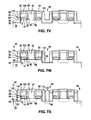
- FIGS. 7A-7Zare cross sectional views of a semiconductor structure showing in sequence the steps in a fourth alternate processing of the semiconductor structure of FIG. 3C in the formation of a non volatile memory array of floating memory cells of the present invention.
- FIGS. 8A-8Ware cross sectional views of a semiconductor structure showing in sequence the steps in a fifth alternate processing of the semiconductor structure of FIG. 7F in the formation of a non volatile memory array of floating memory cells of the present invention.
- the present inventionis a method of forming columns of non-volatile memory cells in active regions that are separated by isolations regions, and an array of memory cells formed thereby.
- the memory cellsutilize a unique memory cell design that allows significant cell size reduction without adversely compromising the erase coupling ratio of the memory cell.
- FIG. 2Athere is shown a top plan view of a semiconductor substrate 10 (or a semiconductor well), which is preferably of P type and is well known in the art.
- a layer of insulating material 12such as silicon dioxide (hereinafter “oxide”), is deposited thereon as shown in FIG. 2 B.
- the insulating layer 12is formed on the substrate 10 by well known techniques such as oxidation or deposition (e.g. chemical vapor deposition or CVD), forming a layer of oxide preferably 80 ⁇ thick.
- a layer of polysilicon 14(hereinafter “poly”) is deposited on top of the layer of insulating material 12 (e.g. 200 to 700 ⁇ thick).
- the deposition and formation of the polysilicon layer 14 on the insulating layer 12can be made by a well known process such as Low Pressure CVD or LPCVD.
- This poly layer 14can be doped by ion implantation or in-Situ doped.
- a silicon nitride layer 18(hereinafter “nitride”) is deposited over the polysilicon layer 14 , preferably by CVD (e.g. 500-1000 ⁇ thick).
- CVDe.g. 500-1000 ⁇ thick
- This nitride layer 18is used to define the active regions during isolation formation.
- all of the forgoing described parameters and the parameters described hereinafterdepend upon the design rules and the process technology generation. What is described herein is for a 0.13 micron process. However, it will be understood by those skilled in the art that the present invention is not limited to any specific process technology generation, nor to any specific value in any of the process parameters described hereinafter.
- suitable photo-resistant material 19is applied on the silicon nitride layer 18 and a masking step is performed to selectively remove the photo-resistant material from certain regions (stripes 16 ).
- the silicon nitride 18 , the polysilicon 14 and the underlying insulating material 12are etched away in stripes 16 formed in the Y or column direction, as shown in FIG. 2C, using standard etching techniques (i.e. anisotropic etch processes).
- the distance W between adjacent stripes 16can be as small as the smallest lithographic feature of the process used.
- the silicon nitride 18 , the polysilicon region 14 and the underlying insulating region 12are maintained.
- the resulting structureis illustrated in FIG. 2D, with active regions 17 interlaced with isolation regions 16 .
- LOCOSlow-oxide-semiconductor
- STIshallow-semiconductor
- the structureis further processed to remove the remaining photo resist 19 .
- an isolation material 20 a or 20 bsuch as silicon dioxide, is formed in the regions or “grooves” 16 .
- the nitride layer 18is then selectively removed to form the structure shown in FIG. 2 E.
- the isolationcan be formed via the well known LOCOS process resulting in the local field oxide 20 a (e.g. by oxidizing the exposed substrate), or it can be formed via a shallow trench process (STI) resulting in silicon-dioxide being formed in the region 20 b (e.g. by depositing an oxide layer, followed by a Chemical-Mechanical-Polishing (CMP) etch).
- STIshallow trench process
- CMPChemical-Mechanical-Polishing
- the substrate 10has alternating stripes of active regions and isolation regions with the isolation regions being formed of either LOCOS insulating material 20 a or shallow trench insulating material 20 b .
- FIG. 2Eshows the formation of both a LOCOS region 20 a and a shallow trench region 20 b , only one of the LOCOS process ( 20 a ) or the shallow trench process ( 20 b ) will be used. In the preferred embodiment, the shallow trench of insulating material 20 b will be formed, because it can be more precisely formed at smaller design rules.
- the structure in FIG. 2Erepresents a self aligned structure, which is more compact than a structure formed by a non self-aligned method.
- a non self-aligned method of forming the structure shown in FIG. 2Eis as follows. Regions of isolation 20 are first formed in the substrate 10 . This can be done by depositing a layer of silicon nitride on the substrate 10 , depositing photo-resist, patterning the silicon nitride using a first masking step to expose selective portions of the substrate 10 , and then oxidizing the exposed substrate 10 using either the LOCOS process or the STI process where silicon trench formation and trench fill are involved. Thereafter, the silicon nitride is removed, and the layer of silicon dioxide 12 (to form the gate oxide) is deposited over the substrate 10 . The layer of polysilicon 14 is deposited over the gate oxide 12 .
- the layer of polysilicon 14is then patterned using a second masking step and selective portions removed.
- the polysilicon 14is not self aligned with the regions of isolation 20 , and a second masking step is required. Further, the additional masking step requires that the dimensions of the polysilicon 14 have an alignment tolerance with respect to the regions of isolation 20 .
- the non self-aligned methoddoes not utilize nitride layer 18 .
- the memory array of the present inventioncan be made by either the self-aligned process or the non self-aligned process.
- FIGS. 3A to 3 Ushow the cross section of the active region structure 17 from a view orthogonal to that of FIGS. 2B and 2E, as the next steps in the process of the present invention are performed. It should be appreciated that while only a small segment of active region 17 is shown, the processing steps illustrated below form an array of such regions.
- An insulating layer 22is first formed on the structure. Specifically, an oxide layer 22 is formed over poly layer 14 (e.g. 100 to 200 ⁇ thick). A thick poly layer 24 is then formed over the oxide layer 22 (e.g. ⁇ 3000 ⁇ thick). The resulting active region structure is shown in FIG. 3 A.
- a conventional photo-lithography (masking) schemeis next used to form semi-recessed first trenches 26 in the structure in the following manner.
- a suitable photo-resistant materialis applied on the poly layer 24 and a masking step is performed to selectively remove the photo-resistant material from selected parallel stripe regions (under which the first trenches 26 will be formed).
- the exposed polysilicon 24is removed using a standard poly etch process (e.g. anisotropic poly etch using oxide layer 22 as an etch stop), leaving blocks of polysilicon 28 with first trenches 26 formed therebetween.
- the width of poly blocks 28can be as small as the smallest lithographic feature of the process used.
- the remaining photo resistis removed, resulting in the structure illustrated in FIG. 3 B.
- a nitride deposition stepis used to form a nitride layer 30 (e.g. 300 to 500 ⁇ thick) over the structure, as illustrated in FIG. 3C.
- a thick oxide layer 32(e.g. 2500 ⁇ thick) is then deposited over nitride layer 30 , as illustrated in FIG. 3D.
- a planarization etch processfollows (e.g. Chemical-Mechanical-Polishing (CMP) etch), which etches the thick oxide layer 32 down even with the tops of poly blocks 28 (using poly blocks 28 as the polishing stopper).
- CMPChemical-Mechanical-Polishing
- the CMP etchalso removes the portions of nitride layer 30 over poly blocks 28 .
- the resulting structureis shown in FIG. 3 E.
- a poly etch processis used to remove poly blocks 28 (using oxide layer 22 as an etch stop) to form second trenches 34 .
- a controlled oxide etchis used to remove the portions of oxide layer 22 exposed at the bottoms of second trenches 34 (using poly layer 14 as an etch stop). This oxide etch also consumes some of thick oxide layer 32 .
- Another poly etch processis performed to remove portions of poly layer 14 exposed at the bottoms of the second trenches 34 (using oxide layer 12 as an etch stop). The resulting structure is shown in FIG. 3 F.
- An oxide sidewall layer 36is formed on the exposed ends of poly layer 14 at trenches 34 using a thermal oxidation process. Suitable ion implantation is then made across the entire surface of the structure. Where the ions have sufficient energy to penetrate exposed portions of oxide layer 12 in each second trench 34 , they then form first regions (source regions) 38 in the substrate 10 having a conductivity type (e.g. N type) that is different from that of the surrounding substrate (e.g. P type). In all other regions, the ions are absorbed by the underlying structure, where they have no effect.
- the implanted source regions 38are self aligned to the second trenches 34 . Sidewall spacers 40 are then formed against the walls of the second trenches 34 .
- Spacers 40can be formed of any dielectric material with good etch selectivity to nitride layer 30 and to substrate silicon 10 .
- insulating spacers 40are formed of oxide by depositing a thin layer of oxide (e.g. 200 ⁇ ) over the entire structure, followed by an anisotropic etch process, such as the well known Reactive Ion Etch (RIE dry etch), to remove the deposited oxide layer except for spacers 40 .
- RIE dry etchReactive Ion Etch
- This oxide etch processalso removes the exposed portions of oxide layer 12 at the bottom of second trenches 34 to expose the substrate 10 , as well as some of oxide layer 32 .
- the resulting structureis shown in FIG. 3 G.
- the second trenchesare filled with poly blocks 42 , preferably in the following manner.
- a thick layer of poly siliconis deposited over the structure.
- a planarization processi.e. CMP
- An optional poly etchmay be performed to slightly recess the upper surfaces of poly blocks 34 relative to nitride layer 30 and oxide layer 32 , to address any topography issues, if present, that can unintentionally short poly blocks 42 to one another.
- the poly blocks 42run across the array columns (along line 1 — 1 in FIG. 2C) and are in direct electrical contact with source regions 38 of substrate 10 .
- the resulting structureis shown in FIG. 3 H.
- Nitride spacers 46are formed against the sidewalls of third trenches 44 by depositing a thick layer of nitride (e.g. 2000 ⁇ ), followed by an anisotropic nitride (RIE dry) etch to remove the deposited nitride except for spacers 46 (e.g. spacers having a width of ⁇ 1500 ⁇ ).
- RIE dryanisotropic nitride
- Oxide layer 48is self aligned to the poly blocks 42 (with a thickness, for example, of ⁇ 600 ⁇ ). During the thermal cycle of this oxidation process, the source regions 38 are driven deeper into the substrate. The resulting structure is shown in FIG. 3 K.
- An anisotropic (dry) nitride etchis used to remove the portions of nitride layer 30 that are exposed in third trenches (between nitride spacers 46 ), using oxide layer 22 as an etch stop. This nitride etch also removes some of the exposed portions of nitride layer 30 adjacent poly blocks 42 and spacers 46 .
- An anisotropic oxide etchfollows to remove the portions of oxide layer 22 that are exposed in third trenches 44 (between nitride spacers 46 ), using poly layer 14 as an etch stop. This oxide etch also slightly consumes small portions of oxide layer 48 . The resulting structure is shown in FIG. 3 L.
- An anisotropic (dry) poly etchis next performed to remove the portions of poly layer 14 that are exposed in third trenches (between nitride spacers 46 ), using oxide layer 12 as an etch stop.
- An anisotropic (dry) oxide etchfollows, which removes the portions of oxide layer 12 that are exposed in third trenches (between nitride spacers 46 ), which exposes the substrate 10 at the bottom of third trenches 44 . This oxide etch also slightly consumes small portions of oxide layer 48 .
- the resulting structureis shown in FIG. 3 M.
- third trenches 44are formed and extend across the active and isolation regions 17 / 16 . Suitable ion implantation is once again made across the entire surface of the structure.
- the ion implantationforms second regions 50 (buried bit-line drain regions) in the active regions of substrate 10 underneath third trenches 44 .
- the ion implantalso has the effect of doping (or further doping) the exposed poly blocks 42 . Outside of third trenches 44 , and except for poly blocks 42 , the ions are blocked and have no effect.
- the resulting structureis shown in FIG. 3 N.
- the second regions 50are not formed under the portions of third trenches that are in the isolation regions, because the ions are blocked by the isolation oxide 20 a or 20 b.
- An oxidation processis then performed, which oxidizes the exposed silicon surfaces of third trenches 44 to form a thin layer of oxide 52 lining these silicon surfaces.
- This oxidation processalso oxidizes the exposed lateral sides 14 a of poly layer 14 that form part of the sidewalls of upper portions of third trenches 44 , which results in horizontally oriented edges 54 each of which points directly toward one of the sidewalls of third trenches 44 , as illustrated in FIG. 3 O.
- Edges 54can be elongated edges (i.e. like the sharp edge of a razor blade), or shorter edges (i.e. like the tip of a pencil). This oxidation process also re-grows the oxide layer 48 over poly blocks 42 .
- poly spacers 56 along sidewalls of third trenches 44follows, which is done by first depositing a poly layer over the structure (e.g. 2000 ⁇ thick). A dry anisotropic dry etch process is then used to remove the deposited poly layer, except for poly spacers 56 left along the sidewalls of third trenches 44 . The resulting structure is shown in FIG. 3 P.
- a nitride etch processis then used to remove nitride spacers 46 .
- An oxide etchfollows to remove oxide layers 48 and 43 , and the exposed portions of oxide layer 52 at the bottom of third trenches 44 (in-between poly spacers 56 ), as shown in FIG. 3Q.
- a nitride etch processfollows (e.g. in hot phosphoric acid), which removes nitride layer 30 , as shown in FIG. 3 R.
- Insulating spacers 58(preferably oxide) are formed along the bottoms of the third trench sidewalls by depositing a layer of oxide over the structure (e.g. 500 to 1200 ⁇ thick), followed by an oxide etch (e.g. RIE). This oxide deposition and etch process also forms oxide spacers 60 adjacent poly spacers 56 (over poly edges 54 ), and oxide spacers 62 adjacent oxide spacers 40 .
- the resulting structureis shown in FIG. 3 S.
- a metal deposition stepis then performed, to deposit a metal such as tungsten, cobalt, titanium, nickel, platinum, or molybdenum over the structure.
- the structureis then annealed, permitting the hot metal to flow and to seep into the exposed portions of the substrate 10 at the bottom of third trenches 44 to form a conductive layer of metalized silicon 64 (silicide) between oxide spacers 58 .
- Metalized silicon regions 64 on substrate 10can be called self aligned silicide (i.e. salicide), because they are self aligned to the second regions 50 by spacers 58 .
- the hot metalalso forms a conductive layer of metalized polysilicon 66 (polycide) on the exposed top portions of poly spacers 56 , and polycide layer 68 on the exposed top portions of poly blocks 42 .
- the metal deposited on the remaining structureis removed by a metal etch process. The resulting structure is shown in FIG. 3 T.
- Passivationsuch as BPSG 70 is used to cover the structure, including filling third trenches 44 .
- a masking stepis performed to define etching areas over the salicide regions 64 .
- the BPSG 70is selectively etched in the etching areas to create contact openings that are ideally centered over the salicide regions 64 (and second regions 50 ).
- the contact openingsare then filled with conductor metal by metal deposition and planarizing etch-back, forming conductor contacts 72 .
- the salicide layer 64enhances conduction between the conductors 72 and the second regions 50 .
- Polycide layers 66 / 68enhance conduction along the length of poly spacers 56 and poly blocks 42 .
- a bit line connector 74is added to each active region by metal masking over the BPSG 70 to connect together all the contacts 72 in that active region. The final structure is shown in FIG. 3 U.
- first and second regions 38 / 50form the source and drain for each cell (although those skilled in the art know that source and drain can be switched during operation).
- Poly layer 14constitutes the floating gate and poly spacer 56 constitutes the control gate for each of the memory cells.
- a channel region 76 for each memory cellis the surface portion of the substrate that is in-between the source and drain 38 / 50 .
- Each channel region 76has two portions joined together at a right angle: a vertical portion 78 extending along the vertical wall of third trench 44 , and a horizontal portion 80 extending between the third trench 44 and the source region 38 .
- Each floating gate 14is disposed over, but insulated from, the horizontal portion 80 of the channel region 76 , and a portion of the source region 38 .
- the floating gates 14each have the horizontally oriented edge 54 that directly faces one of the control gates 56 , but are insulated therefrom by oxide layer 52 .
- the process of the present inventionforms pairs of memory cells that mirror each other, with a memory cell formed on each side of the third trenches 44 that share a common bit-line region 50 .
- each source line region 38which is in electrical contact with poly block 42 , is shared between adjacent memory cells from different mirror sets of memory cells.
- Each control gate 56 , source region 38 (with poly block 42 electrically connected thereto) and drain region 50continuously extend across the isolation regions 16 and active regions 17 , linking together one memory cell from each of the active regions 17 .
- a ground potentialis applied to both its source 38 and drain 50 .
- a high-positive voltage(e.g. +5-10 volts), is applied to the control gate 56 . Electrons on the floating gate 14 are induced through the Fowler-Nordheim tunneling mechanism to tunnel through the oxide layer 52 to the control gate 56 , leaving the floating gate 14 positively charged. Tunneling is enhanced by the horizontally oriented edge 54 formed on each floating gate 14 . It should be noted that since each control gate 56 continuously extends across the active regions 17 and isolation regions 16 , one memory cell from each active region is erased when the high voltage is applied to one of the control gates 56 .
- a small voltage(e.g. 0.5 to 1.0 V) is applied to its drain region 50 .
- a positive voltage level in the vicinity of the threshold voltage of the MOS structure defined by the control gate 56(on the order of approximately +1.8 volts) is applied to its control gate 56 .
- Ground potential and Vddare applied to the source lines 38 and bit-line regions 50 , respectively, for memory cell rows and columns not containing the selected memory cell. Ground potential is applied to the control gates 56 for memory cell rows not containing the selected memory cell. Thus, only the memory cell in the selected row and column is programmed.
- the injection of electrons onto the floating gate 14will continue until the reduction of the charge on the near end of the floating gate 14 can no longer sustain a high surface potential along the horizontal channel region portion 80 to generate hot electrons. At that point, the reduced charge on the floating gate 14 will decrease the electron flow from the drain region 50 onto the floating gate 14 .
- ground potentialis applied to its source region 38 .
- a read voltage of approximately +1 voltis applied to its drain region 50 and approximately 1.5 to 3.3 volts (depending upon the power supply voltage of the device) is applied to its control gate 56 . If the floating gate 14 is positively charged (i.e. the floating gate is discharged of electrons), then the horizontal portion 80 of the channel region 76 (directly underneath the floating gate 14 ) is turned on. When the control gate 56 is raised to the read potential, the vertical portion 78 of the channel region 76 (directly adjacent the control gate 56 ) is also turned on. Thus, the entire channel region 76 will be turned on, causing electrical current to flow from the source region 38 to the drain region 50 . This would be the “1” state.
- the horizontal portion 80 of the channel region 76(directly below the floating gate 14 ) is either weakly turned on or is entirely shut off. Even when the control gate 56 and the drain region 50 are raised to the read potential, little or no current will flow through horizontal portion 80 of channel region 76 . In this case, either the current is very small compared to that of the “1” state or there is no current at all. In this manner, the memory cell is sensed to be programmed at the “0” state. Ground potential is applied to the source lines 38 , bit-line regions 50 , and control gates 56 for non-selected columns and rows so only the selected memory cell is read.
- the memory cell arrayincludes peripheral circuitry including conventional row address decoding circuitry, column address decoding circuitry, sense amplifier circuitry, output buffer circuitry and input buffer circuitry, which are well known in the art.
- the memory cell architecture of the present inventionis advantageous because it does not employ a finite, vertical overlap area between an upwardly extending edge of the floating gate and the control gate.
- a first coupling capacitance C 1laterally between the floating gate 1 and control gate 5
- a second coupling capacitance C 2vertically between the floating gate 1 and control gate 5 .
- the goalis to maximize tunneling efficiency while minimizing capacitive coupling between these two elements.
- C 2can be minimized by reducing the amount of control gate 5 that overhangs floating gate 1 .
- there is a constraint on minimizing C 1 as the floating gatewill have a finite thickness due to fabrication process limitations.
- capacitive coupling C 1serves as a scaling limit.
- this scaling limitis bypassed because the horizontally oriented edge 54 directly faces a vertically oriented control gate spacer 56 disposed laterally adjacent thereto.
- the present inventionalso provides a memory cell array with reduced size and superior program efficiency.
- Memory cell sizeis reduced by as much as 50% because the bit line region 50 is buried inside the substrate 10 , and the bit line regions 50 are self aligned to the third trenches, where space is not wasted due to limitations in the lithography generation, contact alignment and contact integrity.
- Cell areas of approximately 0.21 ⁇ m and 0.14 ⁇ mcan be achieved by the present invention using 0.18 ⁇ m and 0.13 ⁇ m technology generations, respectively.
- Program efficiencyis greatly enhanced by “aiming” the vertical portion 78 of the channel region 76 at the floating gate 14 . In conventional programming schemes, the electrons in the channel region flow in a path parallel to the floating gate, where a relatively small number of the electrons become heated and are injected onto the floating gate.
- the estimated program efficiency(number of electrons injected compared to total number of electrons) is estimated at about ⁇ fraction (1/1000) ⁇ . However, because the first portion of the channel region defines an electron path that is ‘aimed’ directly at the floating gate, the program efficiency of the present invention is estimated to be closer to ⁇ fraction (1/1) ⁇ , where almost all the electrons are injected onto the floating gate.
- control gates formed along the sidewalls of third trenches 44can be separately optimized for conduction performance as well as punch-through immunity without affecting cell size.
- the punch-through suppression between source region 38 and the buried bit-line region 50can be optimized by embedding the source region having a first conductivity type (e.g. N type) in a well having a second conductivity type (e.g. P type) different from the first conductivity type, along with using other sub-surface implant(s) that do not affect the conduction characteristics of the memory cell.
- having source region 38 and bit-line region 50 separated vertically as well as horizontallyallows easier optimization of reliability parameters without affecting cell size.
- the memory cell structure of the present inventionincludes “raised source lines” 42 , meaning that the conductive poly blocks 42 run along (and are electrically connected to) the source lines 38 , but are disposed above the substrate surface.
- the raised source lines 42have sidewalls that are disposed laterally adjacent to sidewalls of floating gates 14 , but are insulated therefrom by oxide layers 36 and oxide spacers 40 . This configuration provides decreased electrical resistance along the length of the source lines 38 , and provides capacitive coupling between the raised source lines 42 and floating gates 14 (in addition to the capacitive coupling caused by the overlap between the floating gates 14 and the source regions 38 ).
- the poly blocks 42are self aligned to the source regions 38 , and the floating gates 14 are self aligned between the poly blocks 42 and the control gate poly spacers 56 (and thus are self aligned to the first and second portions 78 / 80 of the channel regions 76 ).
- FIGS. 4A to 4 Gillustrate a first alternate process for forming the memory cell structure similar to that illustrated in FIG. 3U, where the nitride etch used to remove nitride layer 30 is performed later in the process to preserve part of the nitride layer.
- This first alternate processbegins with the same structure as shown in FIG. 3O, which is shown again in FIG. 4 A.
- poly spacers 56 along sidewalls of third trenches 44is formed in the same way as described above with respect to FIG. 3P, except that a thinner poly layer is preferably deposited over the structure (e.g. 700 ⁇ thick), followed by a dry anisotropic dry etch process to remove the deposited poly layer, except for poly spacers 56 left along the sidewalls of third trenches 44 .
- the poly etchis preferably performed to ensure the top edge of each poly spacer 56 is generally level with the top edge of the adjacent nitride layer 30 (as shown in FIG. 4 B), or is located in-between the adjacent floating gate edge 54 and the adjacent top edge of nitride layer 30 .
- a nitride etch processis then used to remove nitride spacers 46 .
- An oxide etchfollows to remove oxide layers 48 and 43 , and the exposed portions of oxide layer 52 at the bottom of third trenches 44 (in-between poly spacers 56 ), as shown in FIG. 4 C.
- Insulating spacers 58are formed along the sidewalls of third trenches 44 by depositing a layer of oxide over the structure (e.g. 500 to 1200 ⁇ thick), followed by an oxide etch (e.g. RIE). This oxide deposition and etch process also forms oxide spacers 62 adjacent the vertical portions of nitride layer 30 . The resulting structure is shown in FIG. 4 D.
- a metal deposition stepis then performed, to deposit a metal such as tungsten, cobalt, titanium, nickel, platinum, or molybdenum over the structure.
- the structureis then annealed, permitting the hot metal to flow and to seep into the exposed portions of the substrate 10 at the bottom of third trenches 44 to form the salicide layer 64 .
- the hot metalalso forms the polycide layer 66 on the exposed top portions of poly spacers 56 and the polycide layer 68 on the exposed top portions of poly blocks 42 . After a metal etch process to remove the remaining metal, the resulting structure is shown in FIG. 4 E.
- a nitride etch processfollows (e.g. in hot phosphoric acid), which removes exposed portions of nitride layer 30 (i.e. those portions not protected by oxide spacers 62 ), as shown in FIG. 4 F.
- the structureis processed as described above with respect to FIG. 3U (i.e. passivation, contact formation, and bit line formation), to result in the structure shown in FIG. 4 G.
- nitride etch step for removing nitride layer 30is performed later in the process.
- nitride layer 30remains intact to protect oxide layer 22 (over floating gate 14 ) during the salicide/polycide metalization process.
- a portion of the nitride layer 30remains intact in the final memory cell structure (over floating gate 14 and laterally adjacent to poly block 42 ).
- this remaining portion of nitride layer 30provides a stronger sidewall fringing field, and hence enhances the capacitance coupling between the source region 38 (including poly block 42 ) and the floating gate 14 for each of the memory cells.
- FIGS. 5A to 5 Iillustrate a second alternate process for forming the memory cell structure similar to that illustrated in FIG. 3U, where ion implantation used to form second regions 50 is performed later in the process, and an additional tunnel oxide formation is included.
- This second alternate processbegins with the same structure as shown in FIG. 3M, which is shown again in FIG. 5 A.
- the same silicon and oxide etch processesare performed as described above with respect to FIG. 3N to extend third trenches 44 down into substrate 10 , and remove oxide layer 48 , as shown in FIG. 5 B.
- the ion implantation used to form second regions 50is not performed at this time. Instead, the oxidation process as discussed with respect to FIG. 30 is performed to form oxide layer 52 and floating gate edges 54 , and re-grow oxide layer 48 , as illustrated in FIG. 5 C.
- a controlled oxide etch process(e.g. with 10 to 1 diluted HF etchant) is performed to remove oxide layer 52 and expose floating gate pointed edge 54 .
- a thin layer of oxide 82(e.g. 130 ⁇ ) is deposited (e.g. by HTO deposition) over the structure. The removal of oxide layer 52 and deposition of oxide layer 82 provides a tunneling oxide layer adjacent to the pointed edge 54 having a controlled thickness.
- Poly spacers 56are then formed along sidewalls of third trenches 44 by depositing a poly layer over the structure (e.g. 700 ⁇ thick), followed by a dry anisotropic dry etch process to remove the deposited poly layer except for poly spacers 56 left along oxide layer 82 in third trenches 44 .
- the poly etchis performed to ensure the top edge of each poly spacer 56 is generally level with the top edge of the adjacent nitride layer 30 (as shown in FIG. 5 D), or is located in-between the adjacent floating gate edge 54 and the adjacent top edge of nitride layer 30 .
- oxide etch processis then used to remove exposed portions of oxide layer 82 (i.e. those portions not protected by poly spacers 56 ) and oxide layer 48 .
- a nitrideis then used to remove nitride spacers 46 , followed by an oxide etch to remove oxide layer 43 .
- the resulting structureis shown in FIG. 5 E. Suitable ion implantation is made across the entire surface of the structure to form second regions 50 (buried bit-line regions) in the substrate 10 underneath third trenches 44 . Outside of third trenches 44 , the ions are blocked and have no effect.
- the insulating spacers 58(preferably oxide) are formed along the sidewalls of third trenches 44 by depositing a layer of oxide over the structure (e.g.
- oxide deposition and etch processalso forms oxide spacers 62 adjacent the vertical portions of nitride layer 30 .
- the resulting structureis shown in FIG. 5 F. It should be noted that the ion implantation process could be performed after the formation of insulating spacers 58 , or even after forming control gates 56 but before removal of spacers 46 .
- a thermal anneal process(e.g. RTA or furnace thermal anneal) is used to drive the first and second regions 38 / 50 deeper into the substrate 10 .
- a metal deposition stepis then performed, to deposit a metal such as tungsten, cobalt, titanium, nickel, platinum, or molybdenum over the structure.
- the structureis then annealed to form the salicide regions 64 (at the bottom of third trenches 44 between oxide spacers 58 ), to form the polycide regions 66 (over the exposed top portions of poly spacers 56 ), and to form the polycide regions 68 (on the exposed top portions of poly blocks 42 ).
- the metal deposited on the remaining structureis removed by a metal etch process. The resulting structure is shown in FIG. 5 G.
- a nitride etch processfollows (e.g. in hot phosphoric acid), which removes exposed portions of nitride layer 30 (i.e. those portions not protected by oxide spacers 62 ), as shown in FIG. 5 H.
- the structureis then processed as described above with respect to FIG. 3U (i.e. passivation, contact formation, and bit line formation), to result in the structure shown in FIG. 5 I.
- This second alternate embodimentshifts the ion implantation step used to form second regions 50 until after the control gate spacers 56 are formed.
- the oxide layer 82 used for tunneling between the floating gate edge 54 and the control gate 56is formed by an oxide deposition step (e.g. HTO), instead of by a thermal growth step, to better achieve uniformity given the stress induced by the corners of third trenches 44 .
- HTOoxide deposition step
- the remaining portion of the nitride layer 30provides a stronger sidewall fringing field, and hence enhances the capacitance coupling between the source region 38 (including poly block 42 ) and the floating gate 14 .
- FIGS. 6A to 6 Jillustrate a third alternate process for forming the memory cell structure similar to that illustrated in FIG. 3U, and includes “L” shaped control gates and channel regions each having two separate horizontal portions separated by a vertical portion.
- This third alternate processbegins with the same structure as shown in FIG. 3M, which is shown again in FIG. 6 A.
- the same etch processis performed as described above with respect to FIG. 3N to extend third trenches 44 down into substrate 10 , as shown in FIG. 6 B.
- the ion implantation used to form second regions 50is not performed at this time.
- the oxidation process as discussed with respect to FIG. 3Ois performed to form oxide layer 52 and floating gate edges 54 , as illustrated in FIG. 6 C.
- a poly layer 84is formed over the structure.
- An optional polycide layer 86is formed on the upper surface of poly layer 84 , the metal deposition and anneal process discussed above.
- the total thickness of layers 84 and 86is preferably about 700 ⁇ .
- an oxide layeris formed over the structure, followed by an oxide etch that removes the oxide layer except for the oxide spacers 58 formed against poly layer 84 in third trenches 44 .
- the resulting structureis shown in FIG. 6 D.
- a poly etch processis used to remove the exposed portions of polycide layer 86 and poly layer 84 (i.e. portions not protected by oxide spacers 58 ), leaving “L” shaped segments of poly and polycide layers 84 / 86 along the side and bottom walls of trenches 44 .
- this poly etch, and the formation of oxide spacers 58are performed to ensure the top edges of each poly/polycide segment 84 / 86 are generally level with the top edge of the adjacent nitride layer 30 (as shown in FIG. 6 E), or is located in-between the adjacent floating gate edge 54 and the adjacent top edge of nitride layer 30 .
- a nitride etch processis used to remove the exposed nitride spacers 46 .
- An oxide etchis then used to remove oxide spacers 58 (in third trenches 44 ), oxide layer 48 (over poly blocks 42 ), oxide layer 43 , and the portions of oxide layer 52 (at the bottom of third trenches 44 between poly segments 84 ), as shown in FIG. 6 F.
- An oxide deposition and etch back processe.g.
- oxide spacers 88(against exposed and vertically oriented end portions of layers 52 , 84 and 86 in third trenches 44 ), oxide spacers 90 (against vertically oriented portions of polycide layer 86 in third trenches 44 ), and oxide spacers 92 (against vertically oriented portions of nitride layer 30 ).
- Suitable ion implantationis made across the entire surface of the structure to form the second regions 50 (buried bit-line regions) in the substrate 10 underneath third trenches 44 .
- the ionsare also implanted into poly blocks 42 to dope (or further dope) these blocks.
- the ionsare blocked and have no effect. It should be noted that the ion implantation process could be performed before the formation of oxide spacers 88 / 90 / 92 , or before the removal of nitride spacer 46 . The resulting structure is shown in FIG. 6 G.
- a metal deposition stepis then performed, to deposit a metal such as tungsten, cobalt, titanium, nickel, platinum, or molybdenum over the structure.
- the structureis then annealed to form the salicide regions 64 (at the bottom of third trenches 44 between oxide spacers 88 ), the polycide regions 94 (over the exposed top portions of poly layer segments 84 ), and the polycide regions 68 on the exposed top portions of poly blocks 42 .
- the metal deposited on the remaining structureis removed by a metal etch process. The resulting structure is shown in FIG. 6 H.
- a nitride etch processfollows (e.g. in hot phosphoric acid), which removes exposed portions of nitride layer 30 (i.e. those portions not protected by spacers oxide 92 ), as shown in FIG. 61 .
- the structureis then processed as described above with respect to FIG. 3U (i.e. passivation, contact formation, and bit line formation), to result in the structure shown in FIG. 6 J.
- This third alternate embodimentshifts the ion implantation step used to form second regions 50 until after the bottom of third trenches 44 are narrowed by the formation of poly layer segments 84 and polycide 86 .
- second regions 50are formed under only a center portion of the third trench bottom walls. This results in the formation a channel region 76 in the substrate for each cell having three portions joined together at generally right angles, with a first horizontal portion 80 extending between the third trench 44 and the source region 38 , a vertical portion 78 extending along the vertical wall of third trench 44 , and a second horizontal portion 96 extending between the vertical portion 78 and the drain region 50 , so that the channel region 76 is generally “S” shaped.
- control gate thicknessis dictated by a poly deposition step, as opposed to poly deposition and etch back process that can be more difficult to precisely control.
- FIGS. 7A to 7 Zillustrate a fourth alternate process for forming the memory cell structure similar to that illustrated in FIG. 3U, but utilizing a self alignment contact (SAC) scheme.
- This fourth alternate processbegins with the same structure as shown in FIG. 3C, which is shown again in FIG. 7 A.
- a thick layer of dielectric material 102(e.g. BSG) is deposited over the structure, as shown in FIG. 7B, to fill gaps between portions of oxide layer 32 .
- a BSG etch processis used to etch down the BSG layer 102 generally even with the tops of oxide layer 32 , using oxide layer 32 as an etch stop. The BSG etch process results in blocks of the BSG 102 disposed between the tops of oxide layer 32 , as shown in FIG. 7 C.
- An oxide etch processis used to etch the exposed portions of oxide layer 32 down generally even with the tops of nitride layer 30 , using nitride layer 30 as an etch stop.
- a controlled oxide over-etchis used to etch down the exposed portion of oxide layer 32 a predetermined distance below the tops of nitride layer 30 , as shown in FIG. 7 D.
- nitride layer 104is deposited over the structure, as shown in FIG. 7E.
- a planarization etch processfollows (e.g. CMP) to etch down nitride layer 104 , BSG 102 and nitride 30 even with the tops of poly blocks 28 (using poly blocks 28 as the polishing stopper), and to leave the top surfaces of poly blocks 28 exposed.
- CMPplanarization etch process
- a poly etch processis used to remove poly blocks 28 (using oxide layer 22 as an etch stop) to form second trenches 34 .
- a controlled oxide etchis used to remove the portions of oxide layer 22 exposed at the bottoms of second trenches 34 (using poly layer 14 as an etch stop).
- Another poly etch processis performed to remove portions of poly layer 14 exposed at the bottoms of the second trenches 34 (using oxide layer 12 as an etch stop). The resulting structure is shown in FIG. 7 G.
- An oxide sidewall layer 36is formed on the exposed ends of poly layer 14 at trenches 34 using a thermal oxidation process. Suitable ion implantation is then used to form first regions (source regions) 38 in the substrate 10 having a conductivity type (e.g. N type) that is different from that of the surrounding substrate (e.g. P type). Sidewall spacers 40 are then formed against the walls of the second trenches 34 by depositing a thin layer of oxide (e.g. 200 ⁇ ) over the entire structure, followed by an anisotropic etch process (e.g. RIE dry etch), to remove the deposited oxide layer except for spacers 40 . This oxide etch process also removes the exposed portions of oxide layer 12 at the bottom of second trenches 34 to expose the substrate 10 . The resulting structure is shown in FIG. 7 H.
- RIE dry etchanisotropic etch process
- the second trenchesare filled with poly blocks 42 , preferably by depositing a thick layer of poly silicon over the structure, followed by a planarization process (i.e. CMP) to remove the deposited poly silicon except for poly blocks 42 in second trenches 34 .
- CMPplanarization process
- An optional poly etchis be performed to slightly recess the upper surfaces of poly blocks 42 relative to nitride layer 104 and oxide layer 32 , to address any topography issues if present.
- the poly blocks 42are in direct electrical contact with source regions 38 of substrate 10 , and can be doped in-situ or by a separate implant. The resulting structure is shown in FIG. 7 I.
- a BSG etch process(wet or dry) is used to remove BSG 102 , exposing portions of oxide layer 32 .
- An anisotropic etch(e.g. RIE) is then used to remove exposed portions of oxide layer 32 (i.e. portions not protected by nitride 104 ), leaving semi-recessed third trenches 44 disposed between oxide blocks 32 , as illustrated in FIG. 7 J.
- Oxide layer 48is self aligned to the poly blocks 42 (with a thickness, for example, of ⁇ 600 ⁇ ).
- the source regions 38are driven deeper into the substrate.
- the resulting structureis shown in FIG. 7 K.
- An anisotropic (dry) nitride etchis used to remove the portions of nitride layer 30 that are exposed in third trenches (between oxide blocks 32 ), using oxide layer 22 as an etch stop. This nitride etch also removes some of the exposed portions of nitride layer 30 adjacent poly blocks 42 , as well as reducing the thickness of nitride layer 104 (e.g. down to a thickness of ⁇ 300-500 ⁇ ).
- An anisotropic oxide etchfollows to remove the portions of oxide layer 22 that are exposed in third trenches 44 (between oxide blocks 32 ), using poly layer 14 as an etch stop. This oxide etch also slightly consumes small portions of oxide layer 48 . The resulting structure is shown in FIG. 7 L.
- An anisotropic (dry) poly etchis next performed to remove the portions of poly layer 14 that are exposed in third trenches (between oxide blocks 32 ), using oxide layer 12 as an etch stop. This poly etch is preferably performed to form a slope or taper region 106 on the edge of poly layer 14 facing third trenches 44 , as shown in FIG. 7 M.
- An anisotropic (dry) oxide etchfollows, which removes the portions of oxide layer 12 that are exposed in third trenches (between oxide blocks 32 ), which exposes the substrate 10 at the bottom of third trenches 44 . This oxide etch also slightly consumes small portions of oxide layer 48 . The resulting structure is shown in FIG. 7 M.
- a silicon (dry) etch processis performed to extend third trenches 44 down into substrate 10 , to a depth of 500 ⁇ to 1500 ⁇ below the substrate surface.
- This etchis selected to have a 1-to-1 selectivity between silicon and oxide, so that it also etches a similar depth trench in the oxide isolation regions 16 (LOCOS or STI), wherein third trenches 44 are continuously formed and extend across the active and isolation regions 17 / 16 .
- LOCOS or STIoxide isolation regions 16
- An oxidation processis then performed, which oxidizes the exposed silicon surfaces of third trenches 44 to form a thin layer of oxide 52 (e.g. 150 ⁇ ) lining these silicon surfaces.
- This oxidation processalso oxidizes the exposed tapered sides 106 of poly layer 14 that form part of the sidewalls of upper portions of third trenches 44 , which results in horizontally oriented edges 54 each of which points directly toward one of the sidewalls of third trenches 44 , as illustrated in FIG. 7 O.
- Edges 54can be elongated edges (i.e. like the sharp edge of a razor blade), or shorter edges (i.e. like the tip of a pencil). This oxidation process also thickens the oxide layer 48 over poly blocks 42 .
- An optional oxide layer optimization processis next, where the thickness of the thermally grown Fowler-Nordheim tunneling oxide can be optimized by removing oxide layer 52 from the third trenches 44 , followed by an HTO oxide deposition step to reform oxide layer 52 over the entire structure having a well controlled thickness (e.g. 150 ⁇ ).
- a well controlled thicknesse.g. 150 ⁇ .
- a poly layer 56is formed over the structure (e.g. 800 ⁇ thick), as shown in FIG. 7 Q.
- Metalized polysilicon(not shown) can be formed on the upper surface of poly layer 56 .
- a layer of dielectric material 108e.g. BSG, ⁇ 1000 ⁇
- a BSG etch processis then used to etch BSG 108 down even with oxide layer 52 , followed by a poly etch to etch poly layer 56 down even with oxide layer 52 .
- a CMP planarizationcould alternately be used instead of these BSG and poly etches.
- An additional poly etchis performed to recess the tops of poly layer 56 below the tops of oxide layer 52 and BSG 108 , as illustrated in FIG. 7 S.
- a nitride layer 110is next deposited over the structure (e.g. 800 ⁇ ), as shown in FIG. 7T.
- a nitride etchfollows, using oxide layer 52 as an etch stop, which leaves nitride blocks 110 over the poly layer 56 , as shown in FIG. 7 U.
- Nitride blocks 110are self aligned to the poly layer 56 by oxide layer 52 (and oxide block 32 ) and BSG 108 .
- a BSG etchis then used to remove BSG blocks 108 from the third trenches 44 .
- the resulting structureis shown in FIG. 7 V.
- An anisotropic poly etchis used to remove the exposed portions of poly 56 at the bottom of third trenches 44 (i.e. those portions not protected by nitride 110 ), as shown in FIG. 7 W.
- nitrideis deposited over the structure (e.g. 300 ⁇ thick), followed by an anisotropic nitride etch (e.g. RIE) that removes the deposited nitride except for nitride spacers 112 in third trenches 44 .
- Suitable ion implantationis once again made across the entire surface of the structure to form second regions 50 (buried bit-line drain regions) in the substrate 10 underneath third trenches 44 . Outside of third trenches 44 , the ions are blocked and have no effect. It should be noted that the ion implantation process could be performed after the oxide etch performed next. The resulting structure is shown in FIG. 7 X.
- An oxide etch stepis next, which removes the exposed portions of oxide layer 52 and oxide layer 48 .
- a metal deposition stepis then performed, to deposit a metal such as tungsten, cobalt, titanium, nickel, platinum, or molybdenum over the structure.
- the structureis then annealed to form a conductive layer of metalized silicon 64 (silicide) in the exposed substrate between oxide spacers 112 , and a conductive layer of metalized polysilicon 66 (polycide) on the exposed top portions of poly blocks 42 .
- the metal deposited on the remaining structureis removed by a metal etch process.
- the resulting structureis shown in FIG. 7 Y.
- An oxide layer 114(e.g. BP TEOS), is used to cover the structure.
- a masking stepis performed to define etching areas over the salicide regions 64 .
- the oxide layer 114is selectively etched in the etching areas to create contact openings that are ideally centered over the salicide regions 64 (and second regions 50 ).
- the contact openingsare then filled with conductor metal by metal deposition and planarizing etch-back, forming conductor contacts 72 .
- the salicide layer 64enhances conduction between the conductors 72 and the second regions 50 .
- Polycide layer 66enhances conduction along the length of poly blocks 42 .
- a bit line connector 74is added to each active region by metal masking over the oxide 114 to connect together all the contacts 72 in that active region. The final structure is shown in FIG. 7 Z.
- contact 72is referred to as a self aligned contact scheme (SAC) because the width of the contact is made wider than the separation between adjacent, facing nitride spacers 112 , and thus is self aligned to the drain region 50 .
- SACself aligned contact scheme
- Part of the contact 72is formed directly over poly block 56 , but is insulated therefrom by nitride layer 110 , thus ensuring that a good contact with the drain region 50 is achieved.
- the self aligned contact schemeremoves an important constraint on the minimum spacing requirement between adjacent sets of paired memory cells.
- FIG. 7Zillustrates the contact area (and thus conductors 72 ) perfectly centered over the drain regions 50
- a faulty connectioncould occur if the horizontal shift becomes great enough to prevent contact 72 from completely filling in the space between spacers 112 .
- a non-self aligned contact schemesuch as that used with the embodiment illustrated in FIG. 3U, where there is no protective layer of nitride over poly spacers 56 , electrical shorts can occur if the contact 72 is shifted over and makes contact with poly spacers 56 .
- the contact openingsare formed with edges sufficiently away from the spacers 58 so that even with the maximum possible shift in the contact regions, they will not extend beyond the spacers 58 .
- This of coursepresents a constraint on the minimum distance between spacers 58 for the embodiment shown in FIG. 3U, in order to provide a sufficient tolerance distance between adjacent sets of paired mirror cells.
- SAC as used in the fourth alternate embodimenteliminates this constraint by using a protective layer of material (nitride layer 110 ) over poly blocks 56 .
- a protective layer of materialnitride layer 110
- the contact openingsare allowed to be formed in the oxide layer 114 with a sufficient width to ensure there is overlap of the contact opening with the drain regions 50 , even if there is a significant horizontal shift of the contact opening during formation.
- Nitrite layer 110allows portions of contact 72 to be formed over poly blocks 56 without any shorting therebetween. Thus, the width of contact regions between spacers 72 can be minimized, allowing the scaling down of the overall cell dimension. It should be noted that SAC can be utilized with any of the method embodiments illustrated in this application.
- this fourth alternate embodimentresults in second regions 50 being formed under only a center portion of the third trench bottom walls, and thus “S” shaped channel regions 76 have three portions joined together at generally right angles: first horizontal portion 80 extending between the third trench 44 and the source region 38 , vertical portion 78 extending along the vertical wall of third trench 44 , and second horizontal portion 96 extending between the vertical portion 78 and the drain region 50 .
- the generally rectangular control gates 56each have a first portion directly adjacent the channel region vertical portion 78 and a second portion directly adjacent the channel region second horizontal portion 96 .
- FIGS. 8A to 8 Willustrate a fifth alternate process for forming the memory cell structure similar to that illustrated in FIG. 7Z, but with a metal source line scheme. This fifth alternate process begins with the same structure as shown in FIG. 7 F.
- a BSG etch(e.g. wet etch) is used to remove BSG 102 as shown in FIG. 8A, followed by an anisotropic oxide etch (e.g. RIE) that removes exposed portions of oxide layer 32 (i.e. portions not protected by nitride 104 ), leaving semi-recessed third trenches 44 disposed between oxide blocks 32 .
- an anisotropic oxide etche.g. RIE
- the structureis subjected to a thermal oxidation process, which forms an oxide layer 48 over poly blocks 28 .
- Oxide layer 48is self aligned to the poly blocks 28 (with a thickness, for example, of 600 ⁇ ).
- the resulting structureis shown in FIG. 8 B.
- An anisotropic (dry) nitride etchis used to remove the portions of nitride layer 30 that are exposed in third trenches 44 (between oxide blocks 32 ), using oxide layer 22 as an etch stop. This nitride etch also removes some of nitride layer 104 (e.g. leaving a thickness of ⁇ 500 ⁇ ), as well as the exposed portions of nitride layer 30 adjacent poly blocks 28 .
- An anisotropic oxide etchfollows to remove the portions of oxide layer 22 that are exposed in third trenches 44 (between oxide blocks 32 ), using poly layer 14 as an etch stop. This oxide etch also slightly consumes small portions of oxide layer 48 . The resulting structure is shown in FIG. 8 C.
- An anisotropic (dry) poly etchis next performed to remove the portions of poly layer 14 that are exposed in third trenches (between oxide blocks 32 ), using oxide layer 12 as an etch stop. This poly etch is preferably performed to form a slope or taper region 106 on the edge of poly layer 14 facing third trenches 44 , as shown in FIG. 8 D.
- An anisotropic (dry) oxide etchfollows, which removes the portions of oxide layer 12 that are exposed in third trenches 44 (between oxide blocks 32 ), which exposes the substrate 10 at the bottom of third trenches 44 .
- This oxide etchalso slightly consumes small portions of oxide layer 48 .
- a silicon (dry) etch processis performed to extend third trenches 44 down into substrate 10 , to a depth of 500 ⁇ to 1500 ⁇ below the substrate surface.
- This etchis selected to have a 1-to-1 selectivity between silicon and oxide, so that it also etches a similar depth trench in the oxide isolation regions 16 (LOCOS or STI), wherein third trenches 44 are continuously formed and extend across the active and isolation regions 17 / 16 .
- LOCOS or STIoxide isolation regions 16
- An oxidation processis then performed, which oxidizes the exposed silicon surfaces of third trenches 44 to form a thin layer of oxide 52 (e.g. 150 ⁇ ) lining these silicon surfaces.
- This oxidation processalso oxidizes the exposed tapered sides 106 of poly layer 14 that form part of the sidewalls of upper portions of third trenches 44 , which results in horizontally oriented edges 54 each of which points directly toward one of the sidewalls of third trenches 44 , as illustrated in FIG. 8 F.
- Edges 54can be elongated edges (i.e. like the sharp edge of a razor blade), or shorter edges (i.e. like the tip of a pencil). This oxidation process also thickens the oxide layer 48 over poly blocks 42 .
- An optional oxide layer optimization processis next, where the thickness of the thermally grown Fowler-Nordheim tunneling oxide can be optimized by removing oxide layer 52 from the third trenches 44 , followed by an HTO oxide deposition step to reform oxide layer 52 over the entire structure having a well controlled thickness (e.g. 150 ⁇ ).
- a well controlled thicknesse.g. 150 ⁇ .
- a poly layer 56is formed over the structure (e.g. 800 ⁇ thick), as shown in FIG. 8 H.
- Metalized polysilicon(not shown) can be formed on the upper surface of poly layer 56 .
- a layer of dielectric material 108e.g. BSG, ⁇ 1000 ⁇
- a BSG etch processis then used to etch BSG 108 down even with oxide layer 52 , followed by a poly etch to etch poly layer 56 down even with oxide layer 52 .
- a CMP planarizationcould alternately be used instead of these BSG and poly etches.
- An additional poly etchis performed to recess the tops of poly layer 56 below the tops of oxide layer 52 and BSG 108 , as illustrated in FIG. 8 J.
- a nitride layer 110is next deposited over the structure (e.g. 800 ⁇ ), as shown in FIG. 8K.
- a nitride etchfollows, using oxide layer 52 as an etch stop, which leaves nitride blocks 110 over the poly layer 56 , as shown in FIG. 8 L.
- Nitride blocks 110are self aligned to the poly layer 56 by oxide layer 52 (and oxide block 32 ) and BSG 108 .
- a BSG etchis then used to remove BSG blocks 108 from the third trenches 44 .
- the resulting structureis shown in FIG. 8 M.
- An anisotropic poly etchis used to remove the exposed portions of poly 56 at the bottom of third trenches 44 (i.e. those portions not protected by nitride 110 , as shown in FIG. 8 N.
- nitrideis deposited over the structure (e.g. 300 ⁇ thick), followed by an anisotropic nitride etch (e.g. RIE) that removes the deposited nitride except for nitride spacers 112 in third trenches 44 , as illustrated in FIG. 80 .
- Suitable ion implantationis made across the entire surface of the structure to form second regions 50 (buried bit-line drain regions) in the substrate 10 underneath third trenches 44 . Outside of third trenches 44 , the ions are blocked and have no effect. It should be noted that this ion implantation process could be performed at an earlier or a later step in the process. The resulting structure is shown in FIG. 8 P.
- An oxide layer 116is deposited over the structure, which fills third trenches, as shown in FIG. 8 Q.
- the top surface of the structureis planarized (e.g. CMP process) using nitride layer 110 as an etch stop and exposing poly blocks 28 , as shown in FIG. 8 R.
- a poly etch processis used to remove poly blocks 28 (using oxide layer 22 as an etch stop) to form second trenches 34 .
- a controlled oxide etche.g. HF
- Another poly etch processis performed to remove portions of poly layer 14 exposed at the bottoms of the second trenches 34 (using oxide layer 12 as an etch stop).
- Suitable ion implantationis then used to form first regions (source regions) 38 in the substrate 10 having a conductivity type (e.g. N type) that is different from that of the surrounding substrate (e.g. P type).
- the resulting structureis shown in FIG. 8 S.
- An oxide sidewall layer 36is formed on the exposed ends of poly layer 14 at trenches 34 using a thermal oxidation process, as shown in FIG. 8 T.
- Sidewall spacers 40are then formed against the walls of the second trenches 34 by depositing a thin layer of oxide (e.g. 200 ⁇ ) over the entire structure, followed by an anisotropic etch process (e.g. RIE dry etch), to remove the deposited oxide layer except for spacers 40 .
- This oxide etch processalso removes the exposed portions of oxide layer 12 at the bottom of second trenches 34 to expose the substrate 10 , as well as consumes some of oxide layer 52 .
- the resulting structureis shown in FIG. 8 U.
- the second trenches 34are then filled with blocks 120 of metal material in the following manner.
- a layer of TiN material 118is preferably deposited over the structure, followed by the deposition of a thick layer of conductive metal such as aluminum or tungsten. Then, a metal planarization step follows (e.g. CMP), which etches the metal layer down even with the tops of the second trenches 34 , leaving blocks 120 of conductive metal in second trenches 34 and in electrical contact with the source regions 38 via TiN 118 . An optional metal recess etch can be performed to ensure all the metal deposited outside of second trenches 34 has been removed. The resulting structure is shown in FIG. 8 V.
- CMPmetal planarization step
- An oxide layer 114(e.g. BP TEOS), is used to cover the structure.
- a masking stepis performed to define etching areas over the drain regions 50 .
- the oxide layers 114 , 116 , and 52are selectively etched from the etching areas to create contact openings that are ideally centered over and significantly wider than the exposed portions of second region 50 .
- the contact openingsare then filled with conductor metal by metal deposition and planarizing etch-back, forming conductor contacts 72 .
- a bit line connector 74is added to each active region by metal masking over the oxide 114 to connect together all the contacts 72 in that active region.
- the final structureis shown in FIG. 8 W.
- this embodimenthas the further advantage of forming a source line 38 with a block of metallic material attached along its length, thus reducing overall resistance of the source line 38 over its length.
- third trenches 44can end up having any shape that extends into the substrate, not just the elongated rectangular shape shown in the figures.
- third trenches 44can end up having any shape that extends into the substrate, not just the elongated rectangular shape shown in the figures.
- any appropriate conductive materialcan be used.
- any appropriate insulatorcan be used in place of silicon dioxide or silicon nitride.
- any appropriate material whose etch property differs from silicon dioxide (or any insulator) and from polysilicon (or any conductor)can be used in place of silicon nitride.
- the above described inventionis shown to be formed in a substrate which is shown to be uniformly doped, but it is well known and contemplated by the present invention that memory cell elements can be formed in well regions of the substrate too, which are regions that are doped to have a different conductivity type compared to other portions of the substrate.
- single layers of insulating or conductive materialcould be formed as multiple layers of such materials, and vice versa.
Landscapes
- Semiconductor Memories (AREA)
- Non-Volatile Memory (AREA)
Abstract
Description
Claims (44)
Priority Applications (6)
| Application Number | Priority Date | Filing Date | Title |
|---|---|---|---|
| US10/183,834US6756633B2 (en) | 2001-12-27 | 2002-06-25 | Semiconductor memory array of floating gate memory cells with horizontally oriented floating gate edges |
| TW091121356ATW560012B (en) | 2001-12-27 | 2002-09-18 | Self aligned method of forming a semiconductor memory array of floating gate memory cells with horizontally oriented edges, and a memory array made thereby |
| KR1020020084889AKR100559762B1 (en) | 2001-12-27 | 2002-12-27 | Self-aligned method of forming a semiconductor memory array of floating gate memory cells having horizontally oriented edges and a memory array fabricated thereby |
| JP2002380022AJP4004948B2 (en) | 2001-12-27 | 2002-12-27 | Self-aligned method of forming a semiconductor memory array of floating gate memory cells with horizontally oriented edges and memory array formed thereby |
| US10/849,975US6882572B2 (en) | 2001-12-27 | 2004-05-19 | Method of operating a semiconductor memory array of floating gate memory cells with horizontally oriented edges |
| US10/850,031US20040214396A1 (en) | 2001-12-27 | 2004-05-19 | Self aligned method of forming a semiconductor memory array of floating gate memory cells with horizontally oriented edges |
Applications Claiming Priority (3)
| Application Number | Priority Date | Filing Date | Title |
|---|---|---|---|
| US34363401P | 2001-12-27 | 2001-12-27 | |
| US35536302P | 2002-02-06 | 2002-02-06 | |
| US10/183,834US6756633B2 (en) | 2001-12-27 | 2002-06-25 | Semiconductor memory array of floating gate memory cells with horizontally oriented floating gate edges |
Related Child Applications (2)
| Application Number | Title | Priority Date | Filing Date |
|---|---|---|---|
| US10/850,031DivisionUS20040214396A1 (en) | 2001-12-27 | 2004-05-19 | Self aligned method of forming a semiconductor memory array of floating gate memory cells with horizontally oriented edges |
| US10/849,975DivisionUS6882572B2 (en) | 2001-12-27 | 2004-05-19 | Method of operating a semiconductor memory array of floating gate memory cells with horizontally oriented edges |
Publications (2)
| Publication Number | Publication Date |
|---|---|
| US20030122185A1 US20030122185A1 (en) | 2003-07-03 |
| US6756633B2true US6756633B2 (en) | 2004-06-29 |
Family
ID=27391751
Family Applications (3)
| Application Number | Title | Priority Date | Filing Date |
|---|---|---|---|
| US10/183,834Expired - LifetimeUS6756633B2 (en) | 2001-12-27 | 2002-06-25 | Semiconductor memory array of floating gate memory cells with horizontally oriented floating gate edges |
| US10/850,031AbandonedUS20040214396A1 (en) | 2001-12-27 | 2004-05-19 | Self aligned method of forming a semiconductor memory array of floating gate memory cells with horizontally oriented edges |
| US10/849,975Expired - LifetimeUS6882572B2 (en) | 2001-12-27 | 2004-05-19 | Method of operating a semiconductor memory array of floating gate memory cells with horizontally oriented edges |
Family Applications After (2)
| Application Number | Title | Priority Date | Filing Date |
|---|---|---|---|
| US10/850,031AbandonedUS20040214396A1 (en) | 2001-12-27 | 2004-05-19 | Self aligned method of forming a semiconductor memory array of floating gate memory cells with horizontally oriented edges |
| US10/849,975Expired - LifetimeUS6882572B2 (en) | 2001-12-27 | 2004-05-19 | Method of operating a semiconductor memory array of floating gate memory cells with horizontally oriented edges |
Country Status (4)
| Country | Link |
|---|---|
| US (3) | US6756633B2 (en) |
| JP (1) | JP4004948B2 (en) |
| KR (1) | KR100559762B1 (en) |
| TW (1) | TW560012B (en) |
Cited By (252)
| Publication number | Priority date | Publication date | Assignee | Title |
|---|---|---|---|---|
| US20020080965A1 (en)* | 2000-11-28 | 2002-06-27 | Stmicroelectronics S.A. | Random signal generator |
| US20030178668A1 (en)* | 2002-03-20 | 2003-09-25 | Sohrab Kianian | Self aligned method of forming a semiconductor memory array of floating gate memory cells with buried bit-line and raised source line, and a memory array made thereby |
| US20030223296A1 (en)* | 2002-04-05 | 2003-12-04 | Hu Yaw Wen | Self-aligned method of forming a semiconductor memory array of floating gate memory cells with buried source line and floating gate, and a memory array made thereby |
| US20040004863A1 (en)* | 2002-07-05 | 2004-01-08 | Chih-Hsin Wang | Nonvolatile electrically alterable memory device and array made thereby |
| US20040159864A1 (en)* | 2001-10-17 | 2004-08-19 | Sohrab Kianian | Self aligned method of forming a semiconductor memory array of floating gate memory cells with buried bit-line and vertical word line transistor |
| US20040183121A1 (en)* | 2002-04-05 | 2004-09-23 | Bing Yeh | Method of programming electrons onto a floating gate of a non-volatile memory cell |
| US20040262683A1 (en)* | 2003-06-27 | 2004-12-30 | Bohr Mark T. | PMOS transistor strain optimization with raised junction regions |
| US20050045940A1 (en)* | 2003-08-28 | 2005-03-03 | Bomy Chen | Self-aligned method of forming a semiconductor memory array of floating gate memory cells with buried floating gate, and a memory array made thereby |
| US20050104115A1 (en)* | 2002-04-01 | 2005-05-19 | Sohrab Kianian | Self aligned method of forming a semiconductor memory array of floating gate memory cells with buried bit-line and raised source line, and a memory array made thereby |
| US20050169041A1 (en)* | 2003-06-06 | 2005-08-04 | Chih-Hsin Wang | Method of forming floating-gate memory cell having trench structure with ballistic-charge injector, and the array of memory cells made thereby |
| US20050201150A1 (en)* | 2003-06-06 | 2005-09-15 | Chih-Hsin Wang | Method and apparatus for semiconductor device and semiconductor memory device |
| US20060006454A1 (en)* | 2004-07-01 | 2006-01-12 | Chih-Hsin Wang | Electrically alterable memory cell |
| US20060017091A1 (en)* | 2004-07-01 | 2006-01-26 | Chih-Hsin Wang | Method and apparatus for nonvolatile memory |
| US20060146640A1 (en)* | 2004-12-31 | 2006-07-06 | Dongbuanam Semiconductor Inc. | Memory device and method for manufacturing the same |
| US20060289924A1 (en)* | 2005-06-28 | 2006-12-28 | Chih-Hsin Wang | Low power electrically alterable nonvolatile memory cells and arrays |
| US20070008778A1 (en)* | 2003-06-06 | 2007-01-11 | Chih-Hsin Wang | Methods for operating semiconductor device and semiconductor memory device |
| US20070152264A1 (en)* | 2005-12-29 | 2007-07-05 | Dongbu Electronics Co., Ltd. | Nonvolatile memory device and method for fabricating the same |
| US20070281425A1 (en)* | 2003-06-06 | 2007-12-06 | Chih-Hsin Wang | Method and apparatus transporting charges in semiconductor device and semiconductor memory device |
| US20070291539A1 (en)* | 2006-02-01 | 2007-12-20 | Atsuhiro Kinoshita | Nonvolatile semiconductor memory device and manufacturing method thereof |
| US20080203464A1 (en)* | 2004-07-01 | 2008-08-28 | Chih-Hsin Wang | Electrically alterable non-volatile memory and array |
| US20090114999A1 (en)* | 2004-03-05 | 2009-05-07 | Samsung Electroncs Co., Ltd. | Transistors of semiconductor device having channel region in a channel-portion hole and methods of forming the same |
| US20100127308A1 (en)* | 2008-11-26 | 2010-05-27 | Nhan Do | Non-volatile memory cell with self aligned floating and erase gates, and method of making same |
| US20110156118A1 (en)* | 2009-12-30 | 2011-06-30 | Jung-Woo Park | Semiconductor device with vertical cells and fabrication method thereof |
| US8026521B1 (en) | 2010-10-11 | 2011-09-27 | Monolithic 3D Inc. | Semiconductor device and structure |
| US8026574B2 (en) | 2004-05-06 | 2011-09-27 | Sidense Corporation | Anti-fuse memory cell |
| US8072023B1 (en) | 2007-11-12 | 2011-12-06 | Marvell International Ltd. | Isolation for non-volatile memory cell array |
| US8114757B1 (en) | 2010-10-11 | 2012-02-14 | Monolithic 3D Inc. | Semiconductor device and structure |
| US8120088B1 (en) | 2007-12-07 | 2012-02-21 | Marvell International Ltd. | Non-volatile memory cell and array |
| US8163581B1 (en) | 2010-10-13 | 2012-04-24 | Monolith IC 3D | Semiconductor and optoelectronic devices |
| US8237228B2 (en) | 2009-10-12 | 2012-08-07 | Monolithic 3D Inc. | System comprising a semiconductor device and structure |
| US8258810B2 (en) | 2010-09-30 | 2012-09-04 | Monolithic 3D Inc. | 3D semiconductor device |
| US8273610B2 (en) | 2010-11-18 | 2012-09-25 | Monolithic 3D Inc. | Method of constructing a semiconductor device and structure |
| US8283751B2 (en) | 2004-05-06 | 2012-10-09 | Sidense Corp. | Split-channel antifuse array architecture |
| US8283215B2 (en) | 2010-10-13 | 2012-10-09 | Monolithic 3D Inc. | Semiconductor and optoelectronic devices |
| US8294159B2 (en) | 2009-10-12 | 2012-10-23 | Monolithic 3D Inc. | Method for fabrication of a semiconductor device and structure |
| US8298875B1 (en) | 2011-03-06 | 2012-10-30 | Monolithic 3D Inc. | Method for fabrication of a semiconductor device and structure |
| US8362482B2 (en) | 2009-04-14 | 2013-01-29 | Monolithic 3D Inc. | Semiconductor device and structure |
| US8362800B2 (en) | 2010-10-13 | 2013-01-29 | Monolithic 3D Inc. | 3D semiconductor device including field repairable logics |
| US8373439B2 (en) | 2009-04-14 | 2013-02-12 | Monolithic 3D Inc. | 3D semiconductor device |
| US8373230B1 (en) | 2010-10-13 | 2013-02-12 | Monolithic 3D Inc. | Method for fabrication of a semiconductor device and structure |
| US8378494B2 (en) | 2009-04-14 | 2013-02-19 | Monolithic 3D Inc. | Method for fabrication of a semiconductor device and structure |
| US8378715B2 (en) | 2009-04-14 | 2013-02-19 | Monolithic 3D Inc. | Method to construct systems |
| US8379458B1 (en) | 2010-10-13 | 2013-02-19 | Monolithic 3D Inc. | Semiconductor device and structure |
| US8384426B2 (en) | 2009-04-14 | 2013-02-26 | Monolithic 3D Inc. | Semiconductor device and structure |
| US8405420B2 (en) | 2009-04-14 | 2013-03-26 | Monolithic 3D Inc. | System comprising a semiconductor device and structure |
| US8427200B2 (en) | 2009-04-14 | 2013-04-23 | Monolithic 3D Inc. | 3D semiconductor device |
| US8450804B2 (en) | 2011-03-06 | 2013-05-28 | Monolithic 3D Inc. | Semiconductor device and structure for heat removal |
| US8461035B1 (en) | 2010-09-30 | 2013-06-11 | Monolithic 3D Inc. | Method for fabrication of a semiconductor device and structure |
| US8476145B2 (en) | 2010-10-13 | 2013-07-02 | Monolithic 3D Inc. | Method of fabricating a semiconductor device and structure |
| US8492886B2 (en) | 2010-02-16 | 2013-07-23 | Monolithic 3D Inc | 3D integrated circuit with logic |
| US8536023B2 (en) | 2010-11-22 | 2013-09-17 | Monolithic 3D Inc. | Method of manufacturing a semiconductor device and structure |
| US8541819B1 (en) | 2010-12-09 | 2013-09-24 | Monolithic 3D Inc. | Semiconductor device and structure |
| US8557632B1 (en) | 2012-04-09 | 2013-10-15 | Monolithic 3D Inc. | Method for fabrication of a semiconductor device and structure |
| US8574929B1 (en) | 2012-11-16 | 2013-11-05 | Monolithic 3D Inc. | Method to form a 3D semiconductor device and structure |
| US8581349B1 (en) | 2011-05-02 | 2013-11-12 | Monolithic 3D Inc. | 3D memory semiconductor device and structure |
| US8642416B2 (en) | 2010-07-30 | 2014-02-04 | Monolithic 3D Inc. | Method of forming three dimensional integrated circuit devices using layer transfer technique |
| US8669778B1 (en) | 2009-04-14 | 2014-03-11 | Monolithic 3D Inc. | Method for design and manufacturing of a 3D semiconductor device |
| US8674470B1 (en) | 2012-12-22 | 2014-03-18 | Monolithic 3D Inc. | Semiconductor device and structure |
| US8686428B1 (en) | 2012-11-16 | 2014-04-01 | Monolithic 3D Inc. | Semiconductor device and structure |
| US8687399B2 (en) | 2011-10-02 | 2014-04-01 | Monolithic 3D Inc. | Semiconductor device and structure |
| US8709880B2 (en) | 2010-07-30 | 2014-04-29 | Monolithic 3D Inc | Method for fabrication of a semiconductor device and structure |
| US8735297B2 (en) | 2004-05-06 | 2014-05-27 | Sidense Corporation | Reverse optical proximity correction method |
| US8742476B1 (en) | 2012-11-27 | 2014-06-03 | Monolithic 3D Inc. | Semiconductor device and structure |
| US8754533B2 (en) | 2009-04-14 | 2014-06-17 | Monolithic 3D Inc. | Monolithic three-dimensional semiconductor device and structure |
| US8803206B1 (en) | 2012-12-29 | 2014-08-12 | Monolithic 3D Inc. | 3D semiconductor device and structure |
| US8901613B2 (en) | 2011-03-06 | 2014-12-02 | Monolithic 3D Inc. | Semiconductor device and structure for heat removal |
| US8902663B1 (en) | 2013-03-11 | 2014-12-02 | Monolithic 3D Inc. | Method of maintaining a memory state |
| US8975670B2 (en) | 2011-03-06 | 2015-03-10 | Monolithic 3D Inc. | Semiconductor device and structure for heat removal |
| US8994404B1 (en) | 2013-03-12 | 2015-03-31 | Monolithic 3D Inc. | Semiconductor device and structure |
| US9000557B2 (en) | 2012-03-17 | 2015-04-07 | Zvi Or-Bach | Semiconductor device and structure |
| US9029173B2 (en) | 2011-10-18 | 2015-05-12 | Monolithic 3D Inc. | Method for fabrication of a semiconductor device and structure |
| US20150206788A1 (en)* | 2014-01-23 | 2015-07-23 | Silicon Storage Technology, Inc. | Double Patterning Method Of Forming Semiconductor Active Areas And Isolation Regions |
| US9099526B2 (en) | 2010-02-16 | 2015-08-04 | Monolithic 3D Inc. | Integrated circuit device and structure |
| US9099424B1 (en) | 2012-08-10 | 2015-08-04 | Monolithic 3D Inc. | Semiconductor system, device and structure with heat removal |
| US9117749B1 (en) | 2013-03-15 | 2015-08-25 | Monolithic 3D Inc. | Semiconductor device and structure |
| US9123572B2 (en) | 2004-05-06 | 2015-09-01 | Sidense Corporation | Anti-fuse memory cell |
| US9197804B1 (en) | 2011-10-14 | 2015-11-24 | Monolithic 3D Inc. | Semiconductor and optoelectronic devices |
| US9219005B2 (en) | 2011-06-28 | 2015-12-22 | Monolithic 3D Inc. | Semiconductor system and device |
| US9509313B2 (en) | 2009-04-14 | 2016-11-29 | Monolithic 3D Inc. | 3D semiconductor device |
| US9577642B2 (en) | 2009-04-14 | 2017-02-21 | Monolithic 3D Inc. | Method to form a 3D semiconductor device |
| US9711407B2 (en) | 2009-04-14 | 2017-07-18 | Monolithic 3D Inc. | Method of manufacturing a three dimensional integrated circuit by transfer of a mono-crystalline layer |
| US9871034B1 (en) | 2012-12-29 | 2018-01-16 | Monolithic 3D Inc. | Semiconductor device and structure |
| US9953925B2 (en) | 2011-06-28 | 2018-04-24 | Monolithic 3D Inc. | Semiconductor system and device |
| US10043781B2 (en) | 2009-10-12 | 2018-08-07 | Monolithic 3D Inc. | 3D semiconductor device and structure |
| US10115663B2 (en) | 2012-12-29 | 2018-10-30 | Monolithic 3D Inc. | 3D semiconductor device and structure |
| US10127344B2 (en) | 2013-04-15 | 2018-11-13 | Monolithic 3D Inc. | Automation for monolithic 3D devices |
| US10157909B2 (en) | 2009-10-12 | 2018-12-18 | Monolithic 3D Inc. | 3D semiconductor device and structure |
| US10217667B2 (en) | 2011-06-28 | 2019-02-26 | Monolithic 3D Inc. | 3D semiconductor device, fabrication method and system |
| US10224279B2 (en) | 2013-03-15 | 2019-03-05 | Monolithic 3D Inc. | Semiconductor device and structure |
| US10290682B2 (en) | 2010-10-11 | 2019-05-14 | Monolithic 3D Inc. | 3D IC semiconductor device and structure with stacked memory |
| US10297586B2 (en) | 2015-03-09 | 2019-05-21 | Monolithic 3D Inc. | Methods for processing a 3D semiconductor device |
| US10325651B2 (en) | 2013-03-11 | 2019-06-18 | Monolithic 3D Inc. | 3D semiconductor device with stacked memory |
| US10354995B2 (en) | 2009-10-12 | 2019-07-16 | Monolithic 3D Inc. | Semiconductor memory device and structure |
| US10366970B2 (en) | 2009-10-12 | 2019-07-30 | Monolithic 3D Inc. | 3D semiconductor device and structure |
| US10381328B2 (en) | 2015-04-19 | 2019-08-13 | Monolithic 3D Inc. | Semiconductor device and structure |
| US10388863B2 (en) | 2009-10-12 | 2019-08-20 | Monolithic 3D Inc. | 3D memory device and structure |
| US10388568B2 (en) | 2011-06-28 | 2019-08-20 | Monolithic 3D Inc. | 3D semiconductor device and system |
| US10418369B2 (en) | 2015-10-24 | 2019-09-17 | Monolithic 3D Inc. | Multi-level semiconductor memory device and structure |
| US10497713B2 (en) | 2010-11-18 | 2019-12-03 | Monolithic 3D Inc. | 3D semiconductor memory device and structure |
| US10515981B2 (en) | 2015-09-21 | 2019-12-24 | Monolithic 3D Inc. | Multilevel semiconductor device and structure with memory |
| US10522225B1 (en) | 2015-10-02 | 2019-12-31 | Monolithic 3D Inc. | Semiconductor device with non-volatile memory |
| US10600888B2 (en) | 2012-04-09 | 2020-03-24 | Monolithic 3D Inc. | 3D semiconductor device |
| US10600657B2 (en) | 2012-12-29 | 2020-03-24 | Monolithic 3D Inc | 3D semiconductor device and structure |
| US10651054B2 (en) | 2012-12-29 | 2020-05-12 | Monolithic 3D Inc. | 3D semiconductor device and structure |
| US10679977B2 (en) | 2010-10-13 | 2020-06-09 | Monolithic 3D Inc. | 3D microdisplay device and structure |
| US10825779B2 (en) | 2015-04-19 | 2020-11-03 | Monolithic 3D Inc. | 3D semiconductor device and structure |
| US10833108B2 (en) | 2010-10-13 | 2020-11-10 | Monolithic 3D Inc. | 3D microdisplay device and structure |
| US10840239B2 (en) | 2014-08-26 | 2020-11-17 | Monolithic 3D Inc. | 3D semiconductor device and structure |
| US10847540B2 (en) | 2015-10-24 | 2020-11-24 | Monolithic 3D Inc. | 3D semiconductor memory device and structure |
| US10892169B2 (en) | 2012-12-29 | 2021-01-12 | Monolithic 3D Inc. | 3D semiconductor device and structure |
| US10892016B1 (en) | 2019-04-08 | 2021-01-12 | Monolithic 3D Inc. | 3D memory semiconductor devices and structures |
| US10896931B1 (en) | 2010-10-11 | 2021-01-19 | Monolithic 3D Inc. | 3D semiconductor device and structure |
| US10903089B1 (en) | 2012-12-29 | 2021-01-26 | Monolithic 3D Inc. | 3D semiconductor device and structure |
| US10910364B2 (en) | 2009-10-12 | 2021-02-02 | Monolitaic 3D Inc. | 3D semiconductor device |
| US10943934B2 (en) | 2010-10-13 | 2021-03-09 | Monolithic 3D Inc. | Multilevel semiconductor device and structure |
| US10978501B1 (en) | 2010-10-13 | 2021-04-13 | Monolithic 3D Inc. | Multilevel semiconductor device and structure with waveguides |
| US10998374B1 (en) | 2010-10-13 | 2021-05-04 | Monolithic 3D Inc. | Multilevel semiconductor device and structure |
| US11004719B1 (en) | 2010-11-18 | 2021-05-11 | Monolithic 3D Inc. | Methods for producing a 3D semiconductor memory device and structure |
| US11004694B1 (en) | 2012-12-29 | 2021-05-11 | Monolithic 3D Inc. | 3D semiconductor device and structure |
| US11011507B1 (en) | 2015-04-19 | 2021-05-18 | Monolithic 3D Inc. | 3D semiconductor device and structure |
| US11018116B2 (en) | 2012-12-22 | 2021-05-25 | Monolithic 3D Inc. | Method to form a 3D semiconductor device and structure |
| US11018042B1 (en) | 2010-11-18 | 2021-05-25 | Monolithic 3D Inc. | 3D semiconductor memory device and structure |
| US11018191B1 (en) | 2010-10-11 | 2021-05-25 | Monolithic 3D Inc. | 3D semiconductor device and structure |
| US11018133B2 (en) | 2009-10-12 | 2021-05-25 | Monolithic 3D Inc. | 3D integrated circuit |
| US11018156B2 (en) | 2019-04-08 | 2021-05-25 | Monolithic 3D Inc. | 3D memory semiconductor devices and structures |
| US11024673B1 (en) | 2010-10-11 | 2021-06-01 | Monolithic 3D Inc. | 3D semiconductor device and structure |
| US11031275B2 (en) | 2010-11-18 | 2021-06-08 | Monolithic 3D Inc. | 3D semiconductor device and structure with memory |
| US11031394B1 (en) | 2014-01-28 | 2021-06-08 | Monolithic 3D Inc. | 3D semiconductor device and structure |
| US11030371B2 (en) | 2013-04-15 | 2021-06-08 | Monolithic 3D Inc. | Automation for monolithic 3D devices |
| US11043523B1 (en) | 2010-10-13 | 2021-06-22 | Monolithic 3D Inc. | Multilevel semiconductor device and structure with image sensors |
| US11056468B1 (en) | 2015-04-19 | 2021-07-06 | Monolithic 3D Inc. | 3D semiconductor device and structure |
| US11063071B1 (en) | 2010-10-13 | 2021-07-13 | Monolithic 3D Inc. | Multilevel semiconductor device and structure with waveguides |
| US11063024B1 (en) | 2012-12-22 | 2021-07-13 | Monlithic 3D Inc. | Method to form a 3D semiconductor device and structure |
| US11087995B1 (en) | 2012-12-29 | 2021-08-10 | Monolithic 3D Inc. | 3D semiconductor device and structure |
| US11088050B2 (en) | 2012-04-09 | 2021-08-10 | Monolithic 3D Inc. | 3D semiconductor device with isolation layers |
| US11088130B2 (en) | 2014-01-28 | 2021-08-10 | Monolithic 3D Inc. | 3D semiconductor device and structure |
| US11094576B1 (en) | 2010-11-18 | 2021-08-17 | Monolithic 3D Inc. | Methods for producing a 3D semiconductor memory device and structure |
| US11107808B1 (en) | 2014-01-28 | 2021-08-31 | Monolithic 3D Inc. | 3D semiconductor device and structure |
| US11107721B2 (en) | 2010-11-18 | 2021-08-31 | Monolithic 3D Inc. | 3D semiconductor device and structure with NAND logic |
| US11114464B2 (en) | 2015-10-24 | 2021-09-07 | Monolithic 3D Inc. | 3D semiconductor device and structure |
| US11114427B2 (en) | 2015-11-07 | 2021-09-07 | Monolithic 3D Inc. | 3D semiconductor processor and memory device and structure |
| US11121021B2 (en) | 2010-11-18 | 2021-09-14 | Monolithic 3D Inc. | 3D semiconductor device and structure |
| US11133344B2 (en) | 2010-10-13 | 2021-09-28 | Monolithic 3D Inc. | Multilevel semiconductor device and structure with image sensors |
| US11158652B1 (en) | 2019-04-08 | 2021-10-26 | Monolithic 3D Inc. | 3D memory semiconductor devices and structures |
| US11158674B2 (en) | 2010-10-11 | 2021-10-26 | Monolithic 3D Inc. | Method to produce a 3D semiconductor device and structure |
| US11164811B2 (en) | 2012-04-09 | 2021-11-02 | Monolithic 3D Inc. | 3D semiconductor device with isolation layers and oxide-to-oxide bonding |
| US11163112B2 (en) | 2010-10-13 | 2021-11-02 | Monolithic 3D Inc. | Multilevel semiconductor device and structure with electromagnetic modulators |
| US11164898B2 (en) | 2010-10-13 | 2021-11-02 | Monolithic 3D Inc. | Multilevel semiconductor device and structure |
| US11164770B1 (en) | 2010-11-18 | 2021-11-02 | Monolithic 3D Inc. | Method for producing a 3D semiconductor memory device and structure |
| US11177140B2 (en) | 2012-12-29 | 2021-11-16 | Monolithic 3D Inc. | 3D semiconductor device and structure |
| US11211279B2 (en) | 2010-11-18 | 2021-12-28 | Monolithic 3D Inc. | Method for processing a 3D integrated circuit and structure |
| US11217565B2 (en) | 2012-12-22 | 2022-01-04 | Monolithic 3D Inc. | Method to form a 3D semiconductor device and structure |
| US11227897B2 (en) | 2010-10-11 | 2022-01-18 | Monolithic 3D Inc. | Method for producing a 3D semiconductor memory device and structure |
| US11251149B2 (en) | 2016-10-10 | 2022-02-15 | Monolithic 3D Inc. | 3D memory device and structure |
| US11257867B1 (en) | 2010-10-11 | 2022-02-22 | Monolithic 3D Inc. | 3D semiconductor device and structure with oxide bonds |
| US11270055B1 (en) | 2013-04-15 | 2022-03-08 | Monolithic 3D Inc. | Automation for monolithic 3D devices |
| US11296106B2 (en) | 2019-04-08 | 2022-04-05 | Monolithic 3D Inc. | 3D memory semiconductor devices and structures |
| US11296115B1 (en) | 2015-10-24 | 2022-04-05 | Monolithic 3D Inc. | 3D semiconductor device and structure |
| US11309292B2 (en) | 2012-12-22 | 2022-04-19 | Monolithic 3D Inc. | 3D semiconductor device and structure with metal layers |
| US11315980B1 (en) | 2010-10-11 | 2022-04-26 | Monolithic 3D Inc. | 3D semiconductor device and structure with transistors |
| US11327227B2 (en) | 2010-10-13 | 2022-05-10 | Monolithic 3D Inc. | Multilevel semiconductor device and structure with electromagnetic modulators |
| US11329059B1 (en) | 2016-10-10 | 2022-05-10 | Monolithic 3D Inc. | 3D memory devices and structures with thinned single crystal substrates |
| US11341309B1 (en) | 2013-04-15 | 2022-05-24 | Monolithic 3D Inc. | Automation for monolithic 3D devices |
| US11355381B2 (en) | 2010-11-18 | 2022-06-07 | Monolithic 3D Inc. | 3D semiconductor memory device and structure |
| US11355380B2 (en) | 2010-11-18 | 2022-06-07 | Monolithic 3D Inc. | Methods for producing 3D semiconductor memory device and structure utilizing alignment marks |
| US11374118B2 (en) | 2009-10-12 | 2022-06-28 | Monolithic 3D Inc. | Method to form a 3D integrated circuit |
| US11398569B2 (en) | 2013-03-12 | 2022-07-26 | Monolithic 3D Inc. | 3D semiconductor device and structure |
| US11404466B2 (en) | 2010-10-13 | 2022-08-02 | Monolithic 3D Inc. | Multilevel semiconductor device and structure with image sensors |
| US11410912B2 (en) | 2012-04-09 | 2022-08-09 | Monolithic 3D Inc. | 3D semiconductor device with vias and isolation layers |
| US11430668B2 (en) | 2012-12-29 | 2022-08-30 | Monolithic 3D Inc. | 3D semiconductor device and structure with bonding |
| US11430667B2 (en) | 2012-12-29 | 2022-08-30 | Monolithic 3D Inc. | 3D semiconductor device and structure with bonding |
| US11437368B2 (en) | 2010-10-13 | 2022-09-06 | Monolithic 3D Inc. | Multilevel semiconductor device and structure with oxide bonding |
| US11443971B2 (en) | 2010-11-18 | 2022-09-13 | Monolithic 3D Inc. | 3D semiconductor device and structure with memory |
| US11469271B2 (en) | 2010-10-11 | 2022-10-11 | Monolithic 3D Inc. | Method to produce 3D semiconductor devices and structures with memory |
| US11476181B1 (en) | 2012-04-09 | 2022-10-18 | Monolithic 3D Inc. | 3D semiconductor device and structure with metal layers |
| US11482438B2 (en) | 2010-11-18 | 2022-10-25 | Monolithic 3D Inc. | Methods for producing a 3D semiconductor memory device and structure |
| US11482440B2 (en) | 2010-12-16 | 2022-10-25 | Monolithic 3D Inc. | 3D semiconductor device and structure with a built-in test circuit for repairing faulty circuits |
| US11482439B2 (en) | 2010-11-18 | 2022-10-25 | Monolithic 3D Inc. | Methods for producing a 3D semiconductor memory device comprising charge trap junction-less transistors |
| US11487928B2 (en) | 2013-04-15 | 2022-11-01 | Monolithic 3D Inc. | Automation for monolithic 3D devices |
| US11495484B2 (en) | 2010-11-18 | 2022-11-08 | Monolithic 3D Inc. | 3D semiconductor devices and structures with at least two single-crystal layers |
| US11508605B2 (en) | 2010-11-18 | 2022-11-22 | Monolithic 3D Inc. | 3D semiconductor memory device and structure |
| US11521888B2 (en) | 2010-11-18 | 2022-12-06 | Monolithic 3D Inc. | 3D semiconductor device and structure with high-k metal gate transistors |
| US11569117B2 (en) | 2010-11-18 | 2023-01-31 | Monolithic 3D Inc. | 3D semiconductor device and structure with single-crystal layers |
| US11574109B1 (en) | 2013-04-15 | 2023-02-07 | Monolithic 3D Inc | Automation methods for 3D integrated circuits and devices |
| US11594473B2 (en) | 2012-04-09 | 2023-02-28 | Monolithic 3D Inc. | 3D semiconductor device and structure with metal layers and a connective path |
| US11600667B1 (en) | 2010-10-11 | 2023-03-07 | Monolithic 3D Inc. | Method to produce 3D semiconductor devices and structures with memory |
| US11605663B2 (en) | 2010-10-13 | 2023-03-14 | Monolithic 3D Inc. | Multilevel semiconductor device and structure with image sensors and wafer bonding |
| US11610802B2 (en) | 2010-11-18 | 2023-03-21 | Monolithic 3D Inc. | Method for producing a 3D semiconductor device and structure with single crystal transistors and metal gate electrodes |
| US11615977B2 (en) | 2010-11-18 | 2023-03-28 | Monolithic 3D Inc. | 3D semiconductor memory device and structure |
| US11616004B1 (en) | 2012-04-09 | 2023-03-28 | Monolithic 3D Inc. | 3D semiconductor device and structure with metal layers and a connective path |
| US11694944B1 (en) | 2012-04-09 | 2023-07-04 | Monolithic 3D Inc. | 3D semiconductor device and structure with metal layers and a connective path |
| US11694922B2 (en) | 2010-10-13 | 2023-07-04 | Monolithic 3D Inc. | Multilevel semiconductor device and structure with oxide bonding |
| US11711928B2 (en) | 2016-10-10 | 2023-07-25 | Monolithic 3D Inc. | 3D memory devices and structures with control circuits |
| US11720736B2 (en) | 2013-04-15 | 2023-08-08 | Monolithic 3D Inc. | Automation methods for 3D integrated circuits and devices |
| US11735501B1 (en) | 2012-04-09 | 2023-08-22 | Monolithic 3D Inc. | 3D semiconductor device and structure with metal layers and a connective path |
| US11735462B2 (en) | 2010-11-18 | 2023-08-22 | Monolithic 3D Inc. | 3D semiconductor device and structure with single-crystal layers |
| US11763864B2 (en) | 2019-04-08 | 2023-09-19 | Monolithic 3D Inc. | 3D memory semiconductor devices and structures with bit-line pillars |
| US11784169B2 (en) | 2012-12-22 | 2023-10-10 | Monolithic 3D Inc. | 3D semiconductor device and structure with metal layers |
| US11784082B2 (en) | 2010-11-18 | 2023-10-10 | Monolithic 3D Inc. | 3D semiconductor device and structure with bonding |
| US11804396B2 (en) | 2010-11-18 | 2023-10-31 | Monolithic 3D Inc. | Methods for producing a 3D semiconductor device and structure with memory cells and multiple metal layers |
| US11812620B2 (en) | 2016-10-10 | 2023-11-07 | Monolithic 3D Inc. | 3D DRAM memory devices and structures with control circuits |
| US11855100B2 (en) | 2010-10-13 | 2023-12-26 | Monolithic 3D Inc. | Multilevel semiconductor device and structure with oxide bonding |
| US11855114B2 (en) | 2010-10-13 | 2023-12-26 | Monolithic 3D Inc. | Multilevel semiconductor device and structure with image sensors and wafer bonding |
| US11854857B1 (en) | 2010-11-18 | 2023-12-26 | Monolithic 3D Inc. | Methods for producing a 3D semiconductor device and structure with memory cells and multiple metal layers |
| US11862503B2 (en) | 2010-11-18 | 2024-01-02 | Monolithic 3D Inc. | Method for producing a 3D semiconductor device and structure with memory cells and multiple metal layers |
| US11869915B2 (en) | 2010-10-13 | 2024-01-09 | Monolithic 3D Inc. | Multilevel semiconductor device and structure with image sensors and wafer bonding |
| US11869965B2 (en) | 2013-03-11 | 2024-01-09 | Monolithic 3D Inc. | 3D semiconductor device and structure with metal layers and memory cells |
| US11869591B2 (en) | 2016-10-10 | 2024-01-09 | Monolithic 3D Inc. | 3D memory devices and structures with control circuits |
| US11881443B2 (en) | 2012-04-09 | 2024-01-23 | Monolithic 3D Inc. | 3D semiconductor device and structure with metal layers and a connective path |
| US11901210B2 (en) | 2010-11-18 | 2024-02-13 | Monolithic 3D Inc. | 3D semiconductor device and structure with memory |
| US11903187B2 (en) | 2021-04-30 | 2024-02-13 | Samsung Electronics Co., Ltd. | Semiconductor devices |
| US11916045B2 (en) | 2012-12-22 | 2024-02-27 | Monolithic 3D Inc. | 3D semiconductor device and structure with metal layers |
| US11923230B1 (en) | 2010-11-18 | 2024-03-05 | Monolithic 3D Inc. | 3D semiconductor device and structure with bonding |
| US11923374B2 (en) | 2013-03-12 | 2024-03-05 | Monolithic 3D Inc. | 3D semiconductor device and structure with metal layers |
| US11930648B1 (en) | 2016-10-10 | 2024-03-12 | Monolithic 3D Inc. | 3D memory devices and structures with metal layers |
| US11929372B2 (en) | 2010-10-13 | 2024-03-12 | Monolithic 3D Inc. | Multilevel semiconductor device and structure with image sensors and wafer bonding |
| US11937422B2 (en) | 2015-11-07 | 2024-03-19 | Monolithic 3D Inc. | Semiconductor memory device and structure |
| US11935949B1 (en) | 2013-03-11 | 2024-03-19 | Monolithic 3D Inc. | 3D semiconductor device and structure with metal layers and memory cells |
| US11956952B2 (en) | 2015-08-23 | 2024-04-09 | Monolithic 3D Inc. | Semiconductor memory device and structure |
| US11961827B1 (en) | 2012-12-22 | 2024-04-16 | Monolithic 3D Inc. | 3D semiconductor device and structure with metal layers |
| US11967583B2 (en) | 2012-12-22 | 2024-04-23 | Monolithic 3D Inc. | 3D semiconductor device and structure with metal layers |
| US11978731B2 (en) | 2015-09-21 | 2024-05-07 | Monolithic 3D Inc. | Method to produce a multi-level semiconductor memory device and structure |
| US11984445B2 (en) | 2009-10-12 | 2024-05-14 | Monolithic 3D Inc. | 3D semiconductor devices and structures with metal layers |
| US11984438B2 (en) | 2010-10-13 | 2024-05-14 | Monolithic 3D Inc. | Multilevel semiconductor device and structure with oxide bonding |
| US11991884B1 (en) | 2015-10-24 | 2024-05-21 | Monolithic 3D Inc. | 3D semiconductor device and structure with logic and memory |
| US12016181B2 (en) | 2015-10-24 | 2024-06-18 | Monolithic 3D Inc. | 3D semiconductor device and structure with logic and memory |
| US12027518B1 (en) | 2009-10-12 | 2024-07-02 | Monolithic 3D Inc. | 3D semiconductor devices and structures with metal layers |
| US12035531B2 (en) | 2015-10-24 | 2024-07-09 | Monolithic 3D Inc. | 3D semiconductor device and structure with logic and memory |
| US12033884B2 (en) | 2010-11-18 | 2024-07-09 | Monolithic 3D Inc. | Methods for producing a 3D semiconductor device and structure with memory cells and multiple metal layers |
| US12051674B2 (en) | 2012-12-22 | 2024-07-30 | Monolithic 3D Inc. | 3D semiconductor device and structure with metal layers |
| US12068187B2 (en) | 2010-11-18 | 2024-08-20 | Monolithic 3D Inc. | 3D semiconductor device and structure with bonding and DRAM memory cells |
| US12080743B2 (en) | 2010-10-13 | 2024-09-03 | Monolithic 3D Inc. | Multilevel semiconductor device and structure with image sensors and wafer bonding |
| US12094829B2 (en) | 2014-01-28 | 2024-09-17 | Monolithic 3D Inc. | 3D semiconductor device and structure |
| US12094965B2 (en) | 2013-03-11 | 2024-09-17 | Monolithic 3D Inc. | 3D semiconductor device and structure with metal layers and memory cells |
| US12094892B2 (en) | 2010-10-13 | 2024-09-17 | Monolithic 3D Inc. | 3D micro display device and structure |
| US12100646B2 (en) | 2013-03-12 | 2024-09-24 | Monolithic 3D Inc. | 3D semiconductor device and structure with metal layers |
| US12100611B2 (en) | 2010-11-18 | 2024-09-24 | Monolithic 3D Inc. | Methods for producing a 3D semiconductor device and structure with memory cells and multiple metal layers |
| US12100658B2 (en) | 2015-09-21 | 2024-09-24 | Monolithic 3D Inc. | Method to produce a 3D multilayer semiconductor device and structure |
| US12120880B1 (en) | 2015-10-24 | 2024-10-15 | Monolithic 3D Inc. | 3D semiconductor device and structure with logic and memory |
| US12125737B1 (en) | 2010-11-18 | 2024-10-22 | Monolithic 3D Inc. | 3D semiconductor device and structure with metal layers and memory cells |
| US12136562B2 (en) | 2010-11-18 | 2024-11-05 | Monolithic 3D Inc. | 3D semiconductor device and structure with single-crystal layers |
| US12144190B2 (en) | 2010-11-18 | 2024-11-12 | Monolithic 3D Inc. | 3D semiconductor device and structure with bonding and memory cells preliminary class |
| US12154817B1 (en) | 2010-11-18 | 2024-11-26 | Monolithic 3D Inc. | Methods for producing a 3D semiconductor memory device and structure |
| US12178055B2 (en) | 2015-09-21 | 2024-12-24 | Monolithic 3D Inc. | 3D semiconductor memory devices and structures |
| US12219769B2 (en) | 2015-10-24 | 2025-02-04 | Monolithic 3D Inc. | 3D semiconductor device and structure with logic and memory |
| US12225704B2 (en) | 2016-10-10 | 2025-02-11 | Monolithic 3D Inc. | 3D memory devices and structures with memory arrays and metal layers |
| US12243765B2 (en) | 2010-11-18 | 2025-03-04 | Monolithic 3D Inc. | 3D semiconductor device and structure with metal layers and memory cells |
| US12249538B2 (en) | 2012-12-29 | 2025-03-11 | Monolithic 3D Inc. | 3D semiconductor device and structure including power distribution grids |
| US12250830B2 (en) | 2015-09-21 | 2025-03-11 | Monolithic 3D Inc. | 3D semiconductor memory devices and structures |
| US12272586B2 (en) | 2010-11-18 | 2025-04-08 | Monolithic 3D Inc. | 3D semiconductor memory device and structure with memory and metal layers |
| US12362219B2 (en) | 2010-11-18 | 2025-07-15 | Monolithic 3D Inc. | 3D semiconductor memory device and structure |
| US12360310B2 (en) | 2010-10-13 | 2025-07-15 | Monolithic 3D Inc. | Multilevel semiconductor device and structure with oxide bonding |
Families Citing this family (23)
| Publication number | Priority date | Publication date | Assignee | Title |
|---|---|---|---|---|
| US7019353B2 (en) | 2002-07-26 | 2006-03-28 | Micron Technology, Inc. | Three dimensional flash cell |
| KR100467023B1 (en)* | 2002-10-31 | 2005-01-24 | 삼성전자주식회사 | Self-aligned contact structure and method for fabricating the same |
| FR2850205B1 (en)* | 2003-01-22 | 2005-10-07 | St Microelectronics Sa | METHOD FOR MANUFACTURING A FLASH MEMORY AND FLASH MEMORY THUS MANUFACTURED |
| DE10356285A1 (en) | 2003-11-28 | 2005-06-30 | Infineon Technologies Ag | Integrated semiconductor memory and method for manufacturing an integrated semiconductor memory |
| US7098546B1 (en)* | 2004-06-16 | 2006-08-29 | Fasl Llc | Alignment marks with salicided spacers between bitlines for alignment signal improvement |
| US7262093B2 (en)* | 2004-07-15 | 2007-08-28 | Promos Technologies, Inc. | Structure of a non-volatile memory cell and method of forming the same |
| US7071063B2 (en)* | 2004-09-01 | 2006-07-04 | United Microelectronics Corp. | Dual-bit non-volatile memory cell and method of making the same |
| KR100685575B1 (en)* | 2004-12-28 | 2007-02-22 | 주식회사 하이닉스반도체 | Step channel formation method of semiconductor device |
| JP2007005699A (en)* | 2005-06-27 | 2007-01-11 | Matsushita Electric Ind Co Ltd | Nonvolatile semiconductor memory device and manufacturing method thereof |
| US7859026B2 (en)* | 2006-03-16 | 2010-12-28 | Spansion Llc | Vertical semiconductor device |
| US7495280B2 (en) | 2006-05-16 | 2009-02-24 | Taiwan Semiconductor Manufacturing Company, Ltd. | MOS devices with corner spacers |
| US20080142879A1 (en)* | 2006-12-14 | 2008-06-19 | Chartered Semiconductor Manufacturing Ltd. | Integrated circuit system employing differential spacers |
| KR20090004155A (en)* | 2007-07-06 | 2009-01-12 | 삼성전자주식회사 | Nonvolatile Memory Device and Formation Method |
| US7955964B2 (en) | 2008-05-14 | 2011-06-07 | Taiwan Semiconductor Manufacturing Company, Ltd. | Dishing-free gap-filling with multiple CMPs |
| JP2010021465A (en)* | 2008-07-14 | 2010-01-28 | Nec Electronics Corp | Nonvolatile semiconductor memory device |
| US8048752B2 (en)* | 2008-07-24 | 2011-11-01 | Taiwan Semiconductor Manufacturing Company, Ltd. | Spacer shape engineering for void-free gap-filling process |
| GB201112327D0 (en)* | 2011-07-18 | 2011-08-31 | Epigan Nv | Method for growing III-V epitaxial layers |
| US8518818B2 (en)* | 2011-09-16 | 2013-08-27 | Taiwan Semiconductor Manufacturing Co., Ltd. | Reverse damascene process |
| EP2674978B1 (en)* | 2012-06-15 | 2020-07-29 | IMEC vzw | Tunnel field effect transistor device and method for making the device |
| US20150179749A1 (en)* | 2013-12-19 | 2015-06-25 | Silicon Storage Technology, Inc | Non-volatile Memory Cell With Self Aligned Floating And Erase Gates, And Method Of Making Same |
| US9117754B2 (en)* | 2014-01-30 | 2015-08-25 | Freescale Semiconductor, Inc. | Methods for extending floating gates for NVM cells to form sub-lithographic features and related NVM cells |
| US9735245B2 (en)* | 2014-08-25 | 2017-08-15 | Taiwan Semiconductor Manufacturing Co., Ltd. | Recessed salicide structure to integrate a flash memory device with a high κ, metal gate logic device |
| CN111799164B (en)* | 2020-07-20 | 2022-11-04 | 上海华力微电子有限公司 | SONOS memory and manufacturing method thereof |
Citations (27)
| Publication number | Priority date | Publication date | Assignee | Title |
|---|---|---|---|---|
| US4757360A (en) | 1983-07-06 | 1988-07-12 | Rca Corporation | Floating gate memory device with facing asperities on floating and control gates |
| US4794565A (en) | 1986-09-15 | 1988-12-27 | The Regents Of The University Of California | Electrically programmable memory device employing source side injection |
| US4882707A (en) | 1986-10-27 | 1989-11-21 | Kabushiki Kaisha Toshiba | Non-volatile semi-conductor memory device with double gate structure |
| US4905062A (en) | 1987-11-19 | 1990-02-27 | Texas Instruments Incorporated | Planar famos transistor with trench isolation |
| US4931847A (en) | 1986-06-27 | 1990-06-05 | Sgs-Thomson Microelectronics S.P.A. | Floating gate memory with sidewall tunnelling area |
| US4947221A (en) | 1985-11-29 | 1990-08-07 | General Electric Company | Memory cell for a dense EPROM |
| EP0389721A2 (en) | 1989-03-27 | 1990-10-03 | Ict International Cmos Technology, Inc. | Flash EPROM cell and method of making such cell |
| US5021848A (en) | 1990-03-13 | 1991-06-04 | Chiu Te Long | Electrically-erasable and electrically-programmable memory storage devices with self aligned tunnel dielectric area and the method of fabricating thereof |
| US5029130A (en) | 1990-01-22 | 1991-07-02 | Silicon Storage Technology, Inc. | Single transistor non-valatile electrically alterable semiconductor memory device |
| US5041886A (en) | 1989-08-17 | 1991-08-20 | Samsung Electronics Co., Ltd. | Nonvolatile semiconductor memory device and manufacturing method thereof |
| US5101250A (en) | 1988-06-28 | 1992-03-31 | Mitsubishi Denki Kabushiki Kaisha | Electrically programmable non-volatile memory device and manufacturing method thereof |
| US5268319A (en)* | 1988-06-08 | 1993-12-07 | Eliyahou Harari | Highly compact EPROM and flash EEPROM devices |
| US5429965A (en) | 1991-07-08 | 1995-07-04 | Shimoji; Noriyuki | Method for manufacturing a semiconductor memory |
| US5544103A (en) | 1992-03-03 | 1996-08-06 | Xicor, Inc. | Compact page-erasable eeprom non-volatile memory |
| US5572054A (en) | 1990-01-22 | 1996-11-05 | Silicon Storage Technology, Inc. | Method of operating a single transistor non-volatile electrically alterable semiconductor memory device |
| US5780892A (en)* | 1995-03-21 | 1998-07-14 | Winbond Electronics Corporation | Flash E2 PROM cell structure with poly floating and control gates |
| US5780341A (en) | 1996-12-06 | 1998-07-14 | Halo Lsi Design & Device Technology, Inc. | Low voltage EEPROM/NVRAM transistors and making method |
| US5789293A (en) | 1995-03-31 | 1998-08-04 | Samsung Electronics Co., Ltd. | Nonvolatile memory device and manufacturing method thereof |
| US5796139A (en) | 1995-02-23 | 1998-08-18 | Sanyo Electric Co., Ltd. | Semiconductor device |
| US5808328A (en) | 1977-02-21 | 1998-09-15 | Zaidan Hojin Handotai Kenkyu Shinkokai | High-speed and high-density semiconductor memory |
| US5811853A (en) | 1995-12-20 | 1998-09-22 | Winbond Electronics Corp. | Single-side oxide sealed salicide for EPROMS |
| US5814853A (en) | 1996-01-22 | 1998-09-29 | Advanced Micro Devices, Inc. | Sourceless floating gate memory device and method of storing data |
| US6091104A (en) | 1999-03-24 | 2000-07-18 | Chen; Chiou-Feng | Flash memory cell with self-aligned gates and fabrication process |
| US6103573A (en) | 1999-06-30 | 2000-08-15 | Sandisk Corporation | Processing techniques for making a dual floating gate EEPROM cell array |
| US6140182A (en) | 1999-02-23 | 2000-10-31 | Actrans System Inc. | Nonvolatile memory with self-aligned floating gate and fabrication process |
| US6222227B1 (en) | 1999-08-09 | 2001-04-24 | Actrans System Inc. | Memory cell with self-aligned floating gate and separate select gate, and fabrication process |
| US6262917B1 (en) | 1999-10-22 | 2001-07-17 | United Microelectronics Corp. | Structure of a flash memory device |
Family Cites Families (11)
| Publication number | Priority date | Publication date | Assignee | Title |
|---|---|---|---|---|
| US5110753A (en)* | 1988-11-10 | 1992-05-05 | Texas Instruments Incorporated | Cross-point contact-free floating-gate memory array with silicided buried bitlines |
| US5049515A (en)* | 1990-03-09 | 1991-09-17 | Intel Corporation, Inc. | Method of making a three-dimensional memory cell with integral select transistor |
| US5350706A (en)* | 1992-09-30 | 1994-09-27 | Texas Instruments Incorporated | CMOS memory cell array |
| US5455792A (en)* | 1994-09-09 | 1995-10-03 | Yi; Yong-Wan | Flash EEPROM devices employing mid channel injection |
| US6026017A (en)* | 1997-04-11 | 2000-02-15 | Programmable Silicon Solutions | Compact nonvolatile memory |
| US6134144A (en)* | 1997-09-19 | 2000-10-17 | Integrated Memory Technologies, Inc. | Flash memory array |
| US6008089A (en)* | 1997-12-24 | 1999-12-28 | United Semiconductor Corp. | Method of fabricating a split gate flash memory device |
| US6117733A (en)* | 1998-05-27 | 2000-09-12 | Taiwan Semiconductor Manufacturing Company | Poly tip formation and self-align source process for split-gate flash cell |
| US5879992A (en)* | 1998-07-15 | 1999-03-09 | Taiwan Semiconductor Manufacturing Company, Ltd. | Method of fabricating step poly to improve program speed in split gate flash |
| US6426896B1 (en)* | 2000-05-22 | 2002-07-30 | Actrans System Inc. | Flash memory cell with contactless bit line, and process of fabrication |
| US6534818B2 (en)* | 2001-08-07 | 2003-03-18 | Vanguard International Semiconductor Corporation | Stacked-gate flash memory device |
- 2002
- 2002-06-25USUS10/183,834patent/US6756633B2/ennot_activeExpired - Lifetime
- 2002-09-18TWTW091121356Apatent/TW560012B/ennot_activeIP Right Cessation
- 2002-12-27KRKR1020020084889Apatent/KR100559762B1/ennot_activeExpired - Lifetime
- 2002-12-27JPJP2002380022Apatent/JP4004948B2/ennot_activeExpired - Fee Related
- 2004
- 2004-05-19USUS10/850,031patent/US20040214396A1/ennot_activeAbandoned
- 2004-05-19USUS10/849,975patent/US6882572B2/ennot_activeExpired - Lifetime
Patent Citations (27)
| Publication number | Priority date | Publication date | Assignee | Title |
|---|---|---|---|---|
| US5808328A (en) | 1977-02-21 | 1998-09-15 | Zaidan Hojin Handotai Kenkyu Shinkokai | High-speed and high-density semiconductor memory |
| US4757360A (en) | 1983-07-06 | 1988-07-12 | Rca Corporation | Floating gate memory device with facing asperities on floating and control gates |
| US4947221A (en) | 1985-11-29 | 1990-08-07 | General Electric Company | Memory cell for a dense EPROM |
| US4931847A (en) | 1986-06-27 | 1990-06-05 | Sgs-Thomson Microelectronics S.P.A. | Floating gate memory with sidewall tunnelling area |
| US4794565A (en) | 1986-09-15 | 1988-12-27 | The Regents Of The University Of California | Electrically programmable memory device employing source side injection |
| US4882707A (en) | 1986-10-27 | 1989-11-21 | Kabushiki Kaisha Toshiba | Non-volatile semi-conductor memory device with double gate structure |
| US4905062A (en) | 1987-11-19 | 1990-02-27 | Texas Instruments Incorporated | Planar famos transistor with trench isolation |
| US5268319A (en)* | 1988-06-08 | 1993-12-07 | Eliyahou Harari | Highly compact EPROM and flash EEPROM devices |
| US5101250A (en) | 1988-06-28 | 1992-03-31 | Mitsubishi Denki Kabushiki Kaisha | Electrically programmable non-volatile memory device and manufacturing method thereof |
| EP0389721A2 (en) | 1989-03-27 | 1990-10-03 | Ict International Cmos Technology, Inc. | Flash EPROM cell and method of making such cell |
| US5041886A (en) | 1989-08-17 | 1991-08-20 | Samsung Electronics Co., Ltd. | Nonvolatile semiconductor memory device and manufacturing method thereof |
| US5029130A (en) | 1990-01-22 | 1991-07-02 | Silicon Storage Technology, Inc. | Single transistor non-valatile electrically alterable semiconductor memory device |
| US5572054A (en) | 1990-01-22 | 1996-11-05 | Silicon Storage Technology, Inc. | Method of operating a single transistor non-volatile electrically alterable semiconductor memory device |
| US5021848A (en) | 1990-03-13 | 1991-06-04 | Chiu Te Long | Electrically-erasable and electrically-programmable memory storage devices with self aligned tunnel dielectric area and the method of fabricating thereof |
| US5429965A (en) | 1991-07-08 | 1995-07-04 | Shimoji; Noriyuki | Method for manufacturing a semiconductor memory |
| US5544103A (en) | 1992-03-03 | 1996-08-06 | Xicor, Inc. | Compact page-erasable eeprom non-volatile memory |
| US5796139A (en) | 1995-02-23 | 1998-08-18 | Sanyo Electric Co., Ltd. | Semiconductor device |
| US5780892A (en)* | 1995-03-21 | 1998-07-14 | Winbond Electronics Corporation | Flash E2 PROM cell structure with poly floating and control gates |
| US5789293A (en) | 1995-03-31 | 1998-08-04 | Samsung Electronics Co., Ltd. | Nonvolatile memory device and manufacturing method thereof |
| US5811853A (en) | 1995-12-20 | 1998-09-22 | Winbond Electronics Corp. | Single-side oxide sealed salicide for EPROMS |
| US5814853A (en) | 1996-01-22 | 1998-09-29 | Advanced Micro Devices, Inc. | Sourceless floating gate memory device and method of storing data |
| US5780341A (en) | 1996-12-06 | 1998-07-14 | Halo Lsi Design & Device Technology, Inc. | Low voltage EEPROM/NVRAM transistors and making method |
| US6140182A (en) | 1999-02-23 | 2000-10-31 | Actrans System Inc. | Nonvolatile memory with self-aligned floating gate and fabrication process |
| US6091104A (en) | 1999-03-24 | 2000-07-18 | Chen; Chiou-Feng | Flash memory cell with self-aligned gates and fabrication process |
| US6103573A (en) | 1999-06-30 | 2000-08-15 | Sandisk Corporation | Processing techniques for making a dual floating gate EEPROM cell array |
| US6222227B1 (en) | 1999-08-09 | 2001-04-24 | Actrans System Inc. | Memory cell with self-aligned floating gate and separate select gate, and fabrication process |
| US6262917B1 (en) | 1999-10-22 | 2001-07-17 | United Microelectronics Corp. | Structure of a flash memory device |
Non-Patent Citations (1)
| Title |
|---|
| S. Ogura, A. Hori, J. Kato et al., "Low Voltage, Low Current, High Speed Program Step Split gate Cell with Ballistic Direct Injection of r EEPROM/Flash", 0-7803-4777, IEEE, Mar. 1998. |
Cited By (330)
| Publication number | Priority date | Publication date | Assignee | Title |
|---|---|---|---|---|
| US20100180117A1 (en)* | 2000-11-28 | 2010-07-15 | Stmicroelectronics S.A. | Random signal generator |
| US8041950B2 (en) | 2000-11-28 | 2011-10-18 | Stmicroelectronics S.A. | Random signal generator |
| US20020080965A1 (en)* | 2000-11-28 | 2002-06-27 | Stmicroelectronics S.A. | Random signal generator |
| US7706529B2 (en)* | 2000-11-28 | 2010-04-27 | Stmicroelectronics S.A. | Random signal generator |
| US20040159864A1 (en)* | 2001-10-17 | 2004-08-19 | Sohrab Kianian | Self aligned method of forming a semiconductor memory array of floating gate memory cells with buried bit-line and vertical word line transistor |
| US20040160824A1 (en)* | 2001-10-17 | 2004-08-19 | Sohrab Kianian | Method of operating a semiconductor memory array of floating gate memory cells with buried bit-line and vertical word line transistor |
| US7074672B2 (en) | 2001-10-17 | 2006-07-11 | Silicon Storage Technology, Inc. | Self aligned method of forming a semiconductor memory array of floating gate memory cells with buried bit-line and vertical word line transistor |
| US6917069B2 (en) | 2001-10-17 | 2005-07-12 | Silicon Storage Technology, Inc. | Semiconductor memory array of floating gate memory cells with buried bit-line and vertical word line transistor |
| US20030178668A1 (en)* | 2002-03-20 | 2003-09-25 | Sohrab Kianian | Self aligned method of forming a semiconductor memory array of floating gate memory cells with buried bit-line and raised source line, and a memory array made thereby |
| US7144778B2 (en) | 2002-03-20 | 2006-12-05 | Silicon Storage Technology, Inc. | Self aligned method of forming a semiconductor memory array of floating gate memory cells with buried bit-line and raised source line |
| US20040191990A1 (en)* | 2002-03-20 | 2004-09-30 | Sohrab Kianian | Self aligned method of forming a semiconductor memory array of floating gate memory cells with buried bit-line and raised source line |
| US6952033B2 (en)* | 2002-03-20 | 2005-10-04 | Silicon Storage Technology, Inc. | Semiconductor memory array of floating gate memory cells with buried bit-line and raised source line |
| US7326614B2 (en) | 2002-04-01 | 2008-02-05 | Silicon Storage Technology, Inc. | Self aligned method of forming a semiconductor memory array of floating gate memory cells with buried bit-line and raised source line, and a memory array made thereby |
| US20050104115A1 (en)* | 2002-04-01 | 2005-05-19 | Sohrab Kianian | Self aligned method of forming a semiconductor memory array of floating gate memory cells with buried bit-line and raised source line, and a memory array made thereby |
| US7411246B2 (en) | 2002-04-01 | 2008-08-12 | Silicon Storage Technology, Inc. | Self aligned method of forming a semiconductor memory array of floating gate memory cells with buried bit-line and raised source line, and a memory array made thereby |
| US6891220B2 (en) | 2002-04-05 | 2005-05-10 | Silicon Storage Technology, Inc. | Method of programming electrons onto a floating gate of a non-volatile memory cell |
| US7537996B2 (en) | 2002-04-05 | 2009-05-26 | Silicon Storage Technology, Inc. | Self-aligned method of forming a semiconductor memory array of floating gate memory cells with buried source line and floating gate |
| US6952034B2 (en) | 2002-04-05 | 2005-10-04 | Silicon Storage Technology, Inc. | Semiconductor memory array of floating gate memory cells with buried source line and floating gate |
| US20050269624A1 (en)* | 2002-04-05 | 2005-12-08 | Hu Yaw W | Self-aligned method of forming a semiconductor memory array of floating gate memory cells with buried source line and floating gate |
| US20040183121A1 (en)* | 2002-04-05 | 2004-09-23 | Bing Yeh | Method of programming electrons onto a floating gate of a non-volatile memory cell |
| US20030223296A1 (en)* | 2002-04-05 | 2003-12-04 | Hu Yaw Wen | Self-aligned method of forming a semiconductor memory array of floating gate memory cells with buried source line and floating gate, and a memory array made thereby |
| US20040004863A1 (en)* | 2002-07-05 | 2004-01-08 | Chih-Hsin Wang | Nonvolatile electrically alterable memory device and array made thereby |
| US7824981B2 (en) | 2003-06-06 | 2010-11-02 | Chih-Hsin Wang | Method and apparatus for semiconductor device and semiconductor memory device |
| US7297634B2 (en) | 2003-06-06 | 2007-11-20 | Marvell World Trade Ltd. | Method and apparatus for semiconductor device and semiconductor memory device |
| US20050169041A1 (en)* | 2003-06-06 | 2005-08-04 | Chih-Hsin Wang | Method of forming floating-gate memory cell having trench structure with ballistic-charge injector, and the array of memory cells made thereby |
| US7015102B2 (en) | 2003-06-06 | 2006-03-21 | Chih-Hsin Wang | Method of forming floating-gate memory cell having trench structure with ballistic-charge injector, and the array of memory cells made thereby |
| US7550800B2 (en) | 2003-06-06 | 2009-06-23 | Chih-Hsin Wang | Method and apparatus transporting charges in semiconductor device and semiconductor memory device |
| US20070008778A1 (en)* | 2003-06-06 | 2007-01-11 | Chih-Hsin Wang | Methods for operating semiconductor device and semiconductor memory device |
| US7741177B2 (en) | 2003-06-06 | 2010-06-22 | Chih-Hsin Wang | Method and apparatus transporting charges in semiconductor device and semiconductor memory device |
| US7745286B2 (en) | 2003-06-06 | 2010-06-29 | Chih-Hsin Wang | Methods of forming semiconductor devices |
| US20070281425A1 (en)* | 2003-06-06 | 2007-12-06 | Chih-Hsin Wang | Method and apparatus transporting charges in semiconductor device and semiconductor memory device |
| US20080070390A1 (en)* | 2003-06-06 | 2008-03-20 | Chih-Hsin Wang | Method and apparatus for semiconductor device and semiconductor memory device |
| US20050201150A1 (en)* | 2003-06-06 | 2005-09-15 | Chih-Hsin Wang | Method and apparatus for semiconductor device and semiconductor memory device |
| US7613041B2 (en) | 2003-06-06 | 2009-11-03 | Chih-Hsin Wang | Methods for operating semiconductor device and semiconductor memory device |
| US20040262683A1 (en)* | 2003-06-27 | 2004-12-30 | Bohr Mark T. | PMOS transistor strain optimization with raised junction regions |
| US20050045940A1 (en)* | 2003-08-28 | 2005-03-03 | Bomy Chen | Self-aligned method of forming a semiconductor memory array of floating gate memory cells with buried floating gate, and a memory array made thereby |
| US6906379B2 (en) | 2003-08-28 | 2005-06-14 | Silicon Storage Technology, Inc. | Semiconductor memory array of floating gate memory cells with buried floating gate |
| US20090114999A1 (en)* | 2004-03-05 | 2009-05-07 | Samsung Electroncs Co., Ltd. | Transistors of semiconductor device having channel region in a channel-portion hole and methods of forming the same |
| US7696570B2 (en)* | 2004-03-05 | 2010-04-13 | Samsung Electronics Co., Ltd. | Transistors of semiconductor device having channel region in a channel-portion hole and methods of forming the same |
| US8283751B2 (en) | 2004-05-06 | 2012-10-09 | Sidense Corp. | Split-channel antifuse array architecture |
| US8313987B2 (en) | 2004-05-06 | 2012-11-20 | Sidense Corp. | Anti-fuse memory cell |
| US8026574B2 (en) | 2004-05-06 | 2011-09-27 | Sidense Corporation | Anti-fuse memory cell |
| US8735297B2 (en) | 2004-05-06 | 2014-05-27 | Sidense Corporation | Reverse optical proximity correction method |
| US9123572B2 (en) | 2004-05-06 | 2015-09-01 | Sidense Corporation | Anti-fuse memory cell |
| US20060017091A1 (en)* | 2004-07-01 | 2006-01-26 | Chih-Hsin Wang | Method and apparatus for nonvolatile memory |
| US20060006454A1 (en)* | 2004-07-01 | 2006-01-12 | Chih-Hsin Wang | Electrically alterable memory cell |
| US7759719B2 (en) | 2004-07-01 | 2010-07-20 | Chih-Hsin Wang | Electrically alterable memory cell |
| US20080203464A1 (en)* | 2004-07-01 | 2008-08-28 | Chih-Hsin Wang | Electrically alterable non-volatile memory and array |
| US7115942B2 (en) | 2004-07-01 | 2006-10-03 | Chih-Hsin Wang | Method and apparatus for nonvolatile memory |
| US20090317953A1 (en)* | 2004-12-31 | 2009-12-24 | Heung Jin Kim | Memory Device and Method for Manufacturing the Same |
| US20060146640A1 (en)* | 2004-12-31 | 2006-07-06 | Dongbuanam Semiconductor Inc. | Memory device and method for manufacturing the same |
| US20090317952A1 (en)* | 2004-12-31 | 2009-12-24 | Heung Jin Kim | Memory Device and Method for Manufacturing the Same |
| US7598563B2 (en) | 2004-12-31 | 2009-10-06 | Dongbu Electronics Co., Ltd. | Memory device and method for manufacturing the same |
| US7883966B2 (en) | 2004-12-31 | 2011-02-08 | Dongbu Electronics Co., Ltd. | Memory device and method for manufacturing the same |
| US7923326B2 (en) | 2004-12-31 | 2011-04-12 | Dongbu Electronics Co., Ltd. | Memory device and method for manufacturing the same |
| US7719050B1 (en) | 2005-06-28 | 2010-05-18 | Chih-Hsin Wang | Low power electrically alterable nonvolatile memory cells and arrays |
| US20060289924A1 (en)* | 2005-06-28 | 2006-12-28 | Chih-Hsin Wang | Low power electrically alterable nonvolatile memory cells and arrays |
| US7547601B2 (en) | 2005-06-28 | 2009-06-16 | Marvell World Trade Ltd. | Low power electrically alterable nonvolatile memory cells and arrays |
| US7411244B2 (en) | 2005-06-28 | 2008-08-12 | Chih-Hsin Wang | Low power electrically alterable nonvolatile memory cells and arrays |
| US20080061321A1 (en)* | 2005-06-28 | 2008-03-13 | Chih-Hsin Wang | Low power electrically alterable nonvolatile memory cells and arrays |
| US20070152264A1 (en)* | 2005-12-29 | 2007-07-05 | Dongbu Electronics Co., Ltd. | Nonvolatile memory device and method for fabricating the same |
| US20090258466A1 (en)* | 2005-12-29 | 2009-10-15 | Heong Jin Kim | Nonvolatile Memory Device and Method for Fabricating the Same |
| US8021946B2 (en) | 2005-12-29 | 2011-09-20 | Dongbu Electronics Co., Ltd. | Nonvolatile memory device and method for fabricating the same |
| US7566930B2 (en)* | 2005-12-29 | 2009-07-28 | Dongbu Electronics Co., Ltd. | Nonvolatile memory device and method for fabricating the same |
| US7569879B2 (en)* | 2006-02-01 | 2009-08-04 | Kabushiki Kaisha Toshiba | Nonvolatile semiconductor memory device and manufacturing method thereof |
| US20070291539A1 (en)* | 2006-02-01 | 2007-12-20 | Atsuhiro Kinoshita | Nonvolatile semiconductor memory device and manufacturing method thereof |
| US8072023B1 (en) | 2007-11-12 | 2011-12-06 | Marvell International Ltd. | Isolation for non-volatile memory cell array |
| US8120088B1 (en) | 2007-12-07 | 2012-02-21 | Marvell International Ltd. | Non-volatile memory cell and array |
| US20100127308A1 (en)* | 2008-11-26 | 2010-05-27 | Nhan Do | Non-volatile memory cell with self aligned floating and erase gates, and method of making same |
| US8148768B2 (en) | 2008-11-26 | 2012-04-03 | Silicon Storage Technology, Inc. | Non-volatile memory cell with self aligned floating and erase gates, and method of making same |
| US9577642B2 (en) | 2009-04-14 | 2017-02-21 | Monolithic 3D Inc. | Method to form a 3D semiconductor device |
| US8427200B2 (en) | 2009-04-14 | 2013-04-23 | Monolithic 3D Inc. | 3D semiconductor device |
| US8987079B2 (en) | 2009-04-14 | 2015-03-24 | Monolithic 3D Inc. | Method for developing a custom device |
| US8754533B2 (en) | 2009-04-14 | 2014-06-17 | Monolithic 3D Inc. | Monolithic three-dimensional semiconductor device and structure |
| US9509313B2 (en) | 2009-04-14 | 2016-11-29 | Monolithic 3D Inc. | 3D semiconductor device |
| US8378715B2 (en) | 2009-04-14 | 2013-02-19 | Monolithic 3D Inc. | Method to construct systems |
| US8669778B1 (en) | 2009-04-14 | 2014-03-11 | Monolithic 3D Inc. | Method for design and manufacturing of a 3D semiconductor device |
| US9412645B1 (en) | 2009-04-14 | 2016-08-09 | Monolithic 3D Inc. | Semiconductor devices and structures |
| US9711407B2 (en) | 2009-04-14 | 2017-07-18 | Monolithic 3D Inc. | Method of manufacturing a three dimensional integrated circuit by transfer of a mono-crystalline layer |
| US8362482B2 (en) | 2009-04-14 | 2013-01-29 | Monolithic 3D Inc. | Semiconductor device and structure |
| US8405420B2 (en) | 2009-04-14 | 2013-03-26 | Monolithic 3D Inc. | System comprising a semiconductor device and structure |
| US8373439B2 (en) | 2009-04-14 | 2013-02-12 | Monolithic 3D Inc. | 3D semiconductor device |
| US8384426B2 (en) | 2009-04-14 | 2013-02-26 | Monolithic 3D Inc. | Semiconductor device and structure |
| US8378494B2 (en) | 2009-04-14 | 2013-02-19 | Monolithic 3D Inc. | Method for fabrication of a semiconductor device and structure |
| US10366970B2 (en) | 2009-10-12 | 2019-07-30 | Monolithic 3D Inc. | 3D semiconductor device and structure |
| US11984445B2 (en) | 2009-10-12 | 2024-05-14 | Monolithic 3D Inc. | 3D semiconductor devices and structures with metal layers |
| US10354995B2 (en) | 2009-10-12 | 2019-07-16 | Monolithic 3D Inc. | Semiconductor memory device and structure |
| US8395191B2 (en) | 2009-10-12 | 2013-03-12 | Monolithic 3D Inc. | Semiconductor device and structure |
| US10157909B2 (en) | 2009-10-12 | 2018-12-18 | Monolithic 3D Inc. | 3D semiconductor device and structure |
| US10043781B2 (en) | 2009-10-12 | 2018-08-07 | Monolithic 3D Inc. | 3D semiconductor device and structure |
| US11374118B2 (en) | 2009-10-12 | 2022-06-28 | Monolithic 3D Inc. | Method to form a 3D integrated circuit |
| US10388863B2 (en) | 2009-10-12 | 2019-08-20 | Monolithic 3D Inc. | 3D memory device and structure |
| US8907442B2 (en) | 2009-10-12 | 2014-12-09 | Monolthic 3D Inc. | System comprising a semiconductor device and structure |
| US10910364B2 (en) | 2009-10-12 | 2021-02-02 | Monolitaic 3D Inc. | 3D semiconductor device |
| US8294159B2 (en) | 2009-10-12 | 2012-10-23 | Monolithic 3D Inc. | Method for fabrication of a semiconductor device and structure |
| US8664042B2 (en) | 2009-10-12 | 2014-03-04 | Monolithic 3D Inc. | Method for fabrication of configurable systems |
| US9406670B1 (en) | 2009-10-12 | 2016-08-02 | Monolithic 3D Inc. | System comprising a semiconductor device and structure |
| US11018133B2 (en) | 2009-10-12 | 2021-05-25 | Monolithic 3D Inc. | 3D integrated circuit |
| US12027518B1 (en) | 2009-10-12 | 2024-07-02 | Monolithic 3D Inc. | 3D semiconductor devices and structures with metal layers |
| US8237228B2 (en) | 2009-10-12 | 2012-08-07 | Monolithic 3D Inc. | System comprising a semiconductor device and structure |
| US20110156118A1 (en)* | 2009-12-30 | 2011-06-30 | Jung-Woo Park | Semiconductor device with vertical cells and fabrication method thereof |
| US8492886B2 (en) | 2010-02-16 | 2013-07-23 | Monolithic 3D Inc | 3D integrated circuit with logic |
| US9564432B2 (en) | 2010-02-16 | 2017-02-07 | Monolithic 3D Inc. | 3D semiconductor device and structure |
| US9099526B2 (en) | 2010-02-16 | 2015-08-04 | Monolithic 3D Inc. | Integrated circuit device and structure |
| US8846463B1 (en) | 2010-02-16 | 2014-09-30 | Monolithic 3D Inc. | Method to construct a 3D semiconductor device |
| US8642416B2 (en) | 2010-07-30 | 2014-02-04 | Monolithic 3D Inc. | Method of forming three dimensional integrated circuit devices using layer transfer technique |
| US8709880B2 (en) | 2010-07-30 | 2014-04-29 | Monolithic 3D Inc | Method for fabrication of a semiconductor device and structure |
| US8912052B2 (en) | 2010-07-30 | 2014-12-16 | Monolithic 3D Inc. | Semiconductor device and structure |
| US8258810B2 (en) | 2010-09-30 | 2012-09-04 | Monolithic 3D Inc. | 3D semiconductor device |
| US8703597B1 (en) | 2010-09-30 | 2014-04-22 | Monolithic 3D Inc. | Method for fabrication of a semiconductor device and structure |
| US8461035B1 (en) | 2010-09-30 | 2013-06-11 | Monolithic 3D Inc. | Method for fabrication of a semiconductor device and structure |
| US9419031B1 (en) | 2010-10-07 | 2016-08-16 | Monolithic 3D Inc. | Semiconductor and optoelectronic devices |
| US11315980B1 (en) | 2010-10-11 | 2022-04-26 | Monolithic 3D Inc. | 3D semiconductor device and structure with transistors |
| US10290682B2 (en) | 2010-10-11 | 2019-05-14 | Monolithic 3D Inc. | 3D IC semiconductor device and structure with stacked memory |
| US11018191B1 (en) | 2010-10-11 | 2021-05-25 | Monolithic 3D Inc. | 3D semiconductor device and structure |
| US8440542B2 (en) | 2010-10-11 | 2013-05-14 | Monolithic 3D Inc. | Semiconductor device and structure |
| US11158674B2 (en) | 2010-10-11 | 2021-10-26 | Monolithic 3D Inc. | Method to produce a 3D semiconductor device and structure |
| US11024673B1 (en) | 2010-10-11 | 2021-06-01 | Monolithic 3D Inc. | 3D semiconductor device and structure |
| US9818800B2 (en) | 2010-10-11 | 2017-11-14 | Monolithic 3D Inc. | Self aligned semiconductor device and structure |
| US8026521B1 (en) | 2010-10-11 | 2011-09-27 | Monolithic 3D Inc. | Semiconductor device and structure |
| US8114757B1 (en) | 2010-10-11 | 2012-02-14 | Monolithic 3D Inc. | Semiconductor device and structure |
| US8956959B2 (en) | 2010-10-11 | 2015-02-17 | Monolithic 3D Inc. | Method of manufacturing a semiconductor device with two monocrystalline layers |
| US11600667B1 (en) | 2010-10-11 | 2023-03-07 | Monolithic 3D Inc. | Method to produce 3D semiconductor devices and structures with memory |
| US8203148B2 (en) | 2010-10-11 | 2012-06-19 | Monolithic 3D Inc. | Semiconductor device and structure |
| US11227897B2 (en) | 2010-10-11 | 2022-01-18 | Monolithic 3D Inc. | Method for producing a 3D semiconductor memory device and structure |
| US10896931B1 (en) | 2010-10-11 | 2021-01-19 | Monolithic 3D Inc. | 3D semiconductor device and structure |
| US11257867B1 (en) | 2010-10-11 | 2022-02-22 | Monolithic 3D Inc. | 3D semiconductor device and structure with oxide bonds |
| US11469271B2 (en) | 2010-10-11 | 2022-10-11 | Monolithic 3D Inc. | Method to produce 3D semiconductor devices and structures with memory |
| US10679977B2 (en) | 2010-10-13 | 2020-06-09 | Monolithic 3D Inc. | 3D microdisplay device and structure |
| US11437368B2 (en) | 2010-10-13 | 2022-09-06 | Monolithic 3D Inc. | Multilevel semiconductor device and structure with oxide bonding |
| US11063071B1 (en) | 2010-10-13 | 2021-07-13 | Monolithic 3D Inc. | Multilevel semiconductor device and structure with waveguides |
| US10943934B2 (en) | 2010-10-13 | 2021-03-09 | Monolithic 3D Inc. | Multilevel semiconductor device and structure |
| US10978501B1 (en) | 2010-10-13 | 2021-04-13 | Monolithic 3D Inc. | Multilevel semiconductor device and structure with waveguides |
| US10998374B1 (en) | 2010-10-13 | 2021-05-04 | Monolithic 3D Inc. | Multilevel semiconductor device and structure |
| US10833108B2 (en) | 2010-10-13 | 2020-11-10 | Monolithic 3D Inc. | 3D microdisplay device and structure |
| US8823122B2 (en) | 2010-10-13 | 2014-09-02 | Monolithic 3D Inc. | Semiconductor and optoelectronic devices |
| US12094892B2 (en) | 2010-10-13 | 2024-09-17 | Monolithic 3D Inc. | 3D micro display device and structure |
| US11984438B2 (en) | 2010-10-13 | 2024-05-14 | Monolithic 3D Inc. | Multilevel semiconductor device and structure with oxide bonding |
| US12360310B2 (en) | 2010-10-13 | 2025-07-15 | Monolithic 3D Inc. | Multilevel semiconductor device and structure with oxide bonding |
| US11929372B2 (en) | 2010-10-13 | 2024-03-12 | Monolithic 3D Inc. | Multilevel semiconductor device and structure with image sensors and wafer bonding |
| US11164898B2 (en) | 2010-10-13 | 2021-11-02 | Monolithic 3D Inc. | Multilevel semiconductor device and structure |
| US11043523B1 (en) | 2010-10-13 | 2021-06-22 | Monolithic 3D Inc. | Multilevel semiconductor device and structure with image sensors |
| US11163112B2 (en) | 2010-10-13 | 2021-11-02 | Monolithic 3D Inc. | Multilevel semiconductor device and structure with electromagnetic modulators |
| US12080743B2 (en) | 2010-10-13 | 2024-09-03 | Monolithic 3D Inc. | Multilevel semiconductor device and structure with image sensors and wafer bonding |
| US11605663B2 (en) | 2010-10-13 | 2023-03-14 | Monolithic 3D Inc. | Multilevel semiconductor device and structure with image sensors and wafer bonding |
| US11869915B2 (en) | 2010-10-13 | 2024-01-09 | Monolithic 3D Inc. | Multilevel semiconductor device and structure with image sensors and wafer bonding |
| US8163581B1 (en) | 2010-10-13 | 2012-04-24 | Monolith IC 3D | Semiconductor and optoelectronic devices |
| US8476145B2 (en) | 2010-10-13 | 2013-07-02 | Monolithic 3D Inc. | Method of fabricating a semiconductor device and structure |
| US11404466B2 (en) | 2010-10-13 | 2022-08-02 | Monolithic 3D Inc. | Multilevel semiconductor device and structure with image sensors |
| US8283215B2 (en) | 2010-10-13 | 2012-10-09 | Monolithic 3D Inc. | Semiconductor and optoelectronic devices |
| US11327227B2 (en) | 2010-10-13 | 2022-05-10 | Monolithic 3D Inc. | Multilevel semiconductor device and structure with electromagnetic modulators |
| US11374042B1 (en) | 2010-10-13 | 2022-06-28 | Monolithic 3D Inc. | 3D micro display semiconductor device and structure |
| US8379458B1 (en) | 2010-10-13 | 2013-02-19 | Monolithic 3D Inc. | Semiconductor device and structure |
| US8753913B2 (en) | 2010-10-13 | 2014-06-17 | Monolithic 3D Inc. | Method for fabricating novel semiconductor and optoelectronic devices |
| US11133344B2 (en) | 2010-10-13 | 2021-09-28 | Monolithic 3D Inc. | Multilevel semiconductor device and structure with image sensors |
| US11855114B2 (en) | 2010-10-13 | 2023-12-26 | Monolithic 3D Inc. | Multilevel semiconductor device and structure with image sensors and wafer bonding |
| US11855100B2 (en) | 2010-10-13 | 2023-12-26 | Monolithic 3D Inc. | Multilevel semiconductor device and structure with oxide bonding |
| US8362800B2 (en) | 2010-10-13 | 2013-01-29 | Monolithic 3D Inc. | 3D semiconductor device including field repairable logics |
| US8373230B1 (en) | 2010-10-13 | 2013-02-12 | Monolithic 3D Inc. | Method for fabrication of a semiconductor device and structure |
| US11694922B2 (en) | 2010-10-13 | 2023-07-04 | Monolithic 3D Inc. | Multilevel semiconductor device and structure with oxide bonding |
| US12125737B1 (en) | 2010-11-18 | 2024-10-22 | Monolithic 3D Inc. | 3D semiconductor device and structure with metal layers and memory cells |
| US11031275B2 (en) | 2010-11-18 | 2021-06-08 | Monolithic 3D Inc. | 3D semiconductor device and structure with memory |
| US11735462B2 (en) | 2010-11-18 | 2023-08-22 | Monolithic 3D Inc. | 3D semiconductor device and structure with single-crystal layers |
| US11804396B2 (en) | 2010-11-18 | 2023-10-31 | Monolithic 3D Inc. | Methods for producing a 3D semiconductor device and structure with memory cells and multiple metal layers |
| US11107721B2 (en) | 2010-11-18 | 2021-08-31 | Monolithic 3D Inc. | 3D semiconductor device and structure with NAND logic |
| US11094576B1 (en) | 2010-11-18 | 2021-08-17 | Monolithic 3D Inc. | Methods for producing a 3D semiconductor memory device and structure |
| US11854857B1 (en) | 2010-11-18 | 2023-12-26 | Monolithic 3D Inc. | Methods for producing a 3D semiconductor device and structure with memory cells and multiple metal layers |
| US11862503B2 (en) | 2010-11-18 | 2024-01-02 | Monolithic 3D Inc. | Method for producing a 3D semiconductor device and structure with memory cells and multiple metal layers |
| US11164770B1 (en) | 2010-11-18 | 2021-11-02 | Monolithic 3D Inc. | Method for producing a 3D semiconductor memory device and structure |
| US11615977B2 (en) | 2010-11-18 | 2023-03-28 | Monolithic 3D Inc. | 3D semiconductor memory device and structure |
| US10497713B2 (en) | 2010-11-18 | 2019-12-03 | Monolithic 3D Inc. | 3D semiconductor memory device and structure |
| US11610802B2 (en) | 2010-11-18 | 2023-03-21 | Monolithic 3D Inc. | Method for producing a 3D semiconductor device and structure with single crystal transistors and metal gate electrodes |
| US11901210B2 (en) | 2010-11-18 | 2024-02-13 | Monolithic 3D Inc. | 3D semiconductor device and structure with memory |
| US11923230B1 (en) | 2010-11-18 | 2024-03-05 | Monolithic 3D Inc. | 3D semiconductor device and structure with bonding |
| US11569117B2 (en) | 2010-11-18 | 2023-01-31 | Monolithic 3D Inc. | 3D semiconductor device and structure with single-crystal layers |
| US11521888B2 (en) | 2010-11-18 | 2022-12-06 | Monolithic 3D Inc. | 3D semiconductor device and structure with high-k metal gate transistors |
| US11211279B2 (en) | 2010-11-18 | 2021-12-28 | Monolithic 3D Inc. | Method for processing a 3D integrated circuit and structure |
| US11508605B2 (en) | 2010-11-18 | 2022-11-22 | Monolithic 3D Inc. | 3D semiconductor memory device and structure |
| US12362219B2 (en) | 2010-11-18 | 2025-07-15 | Monolithic 3D Inc. | 3D semiconductor memory device and structure |
| US11495484B2 (en) | 2010-11-18 | 2022-11-08 | Monolithic 3D Inc. | 3D semiconductor devices and structures with at least two single-crystal layers |
| US11482439B2 (en) | 2010-11-18 | 2022-10-25 | Monolithic 3D Inc. | Methods for producing a 3D semiconductor memory device comprising charge trap junction-less transistors |
| US12272586B2 (en) | 2010-11-18 | 2025-04-08 | Monolithic 3D Inc. | 3D semiconductor memory device and structure with memory and metal layers |
| US11482438B2 (en) | 2010-11-18 | 2022-10-25 | Monolithic 3D Inc. | Methods for producing a 3D semiconductor memory device and structure |
| US9136153B2 (en) | 2010-11-18 | 2015-09-15 | Monolithic 3D Inc. | 3D semiconductor device and structure with back-bias |
| US12033884B2 (en) | 2010-11-18 | 2024-07-09 | Monolithic 3D Inc. | Methods for producing a 3D semiconductor device and structure with memory cells and multiple metal layers |
| US12068187B2 (en) | 2010-11-18 | 2024-08-20 | Monolithic 3D Inc. | 3D semiconductor device and structure with bonding and DRAM memory cells |
| US12243765B2 (en) | 2010-11-18 | 2025-03-04 | Monolithic 3D Inc. | 3D semiconductor device and structure with metal layers and memory cells |
| US11443971B2 (en) | 2010-11-18 | 2022-09-13 | Monolithic 3D Inc. | 3D semiconductor device and structure with memory |
| US12154817B1 (en) | 2010-11-18 | 2024-11-26 | Monolithic 3D Inc. | Methods for producing a 3D semiconductor memory device and structure |
| US11355381B2 (en) | 2010-11-18 | 2022-06-07 | Monolithic 3D Inc. | 3D semiconductor memory device and structure |
| US11004719B1 (en) | 2010-11-18 | 2021-05-11 | Monolithic 3D Inc. | Methods for producing a 3D semiconductor memory device and structure |
| US11784082B2 (en) | 2010-11-18 | 2023-10-10 | Monolithic 3D Inc. | 3D semiconductor device and structure with bonding |
| US12100611B2 (en) | 2010-11-18 | 2024-09-24 | Monolithic 3D Inc. | Methods for producing a 3D semiconductor device and structure with memory cells and multiple metal layers |
| US11121021B2 (en) | 2010-11-18 | 2021-09-14 | Monolithic 3D Inc. | 3D semiconductor device and structure |
| US8273610B2 (en) | 2010-11-18 | 2012-09-25 | Monolithic 3D Inc. | Method of constructing a semiconductor device and structure |
| US11018042B1 (en) | 2010-11-18 | 2021-05-25 | Monolithic 3D Inc. | 3D semiconductor memory device and structure |
| US12136562B2 (en) | 2010-11-18 | 2024-11-05 | Monolithic 3D Inc. | 3D semiconductor device and structure with single-crystal layers |
| US12144190B2 (en) | 2010-11-18 | 2024-11-12 | Monolithic 3D Inc. | 3D semiconductor device and structure with bonding and memory cells preliminary class |
| US11355380B2 (en) | 2010-11-18 | 2022-06-07 | Monolithic 3D Inc. | Methods for producing 3D semiconductor memory device and structure utilizing alignment marks |
| US8536023B2 (en) | 2010-11-22 | 2013-09-17 | Monolithic 3D Inc. | Method of manufacturing a semiconductor device and structure |
| US8541819B1 (en) | 2010-12-09 | 2013-09-24 | Monolithic 3D Inc. | Semiconductor device and structure |
| US11482440B2 (en) | 2010-12-16 | 2022-10-25 | Monolithic 3D Inc. | 3D semiconductor device and structure with a built-in test circuit for repairing faulty circuits |
| US8975670B2 (en) | 2011-03-06 | 2015-03-10 | Monolithic 3D Inc. | Semiconductor device and structure for heat removal |
| US8298875B1 (en) | 2011-03-06 | 2012-10-30 | Monolithic 3D Inc. | Method for fabrication of a semiconductor device and structure |
| US8450804B2 (en) | 2011-03-06 | 2013-05-28 | Monolithic 3D Inc. | Semiconductor device and structure for heat removal |
| US8901613B2 (en) | 2011-03-06 | 2014-12-02 | Monolithic 3D Inc. | Semiconductor device and structure for heat removal |
| US8581349B1 (en) | 2011-05-02 | 2013-11-12 | Monolithic 3D Inc. | 3D memory semiconductor device and structure |
| US10217667B2 (en) | 2011-06-28 | 2019-02-26 | Monolithic 3D Inc. | 3D semiconductor device, fabrication method and system |
| US9219005B2 (en) | 2011-06-28 | 2015-12-22 | Monolithic 3D Inc. | Semiconductor system and device |
| US10388568B2 (en) | 2011-06-28 | 2019-08-20 | Monolithic 3D Inc. | 3D semiconductor device and system |
| US9953925B2 (en) | 2011-06-28 | 2018-04-24 | Monolithic 3D Inc. | Semiconductor system and device |
| US8687399B2 (en) | 2011-10-02 | 2014-04-01 | Monolithic 3D Inc. | Semiconductor device and structure |
| US9030858B2 (en) | 2011-10-02 | 2015-05-12 | Monolithic 3D Inc. | Semiconductor device and structure |
| US9197804B1 (en) | 2011-10-14 | 2015-11-24 | Monolithic 3D Inc. | Semiconductor and optoelectronic devices |
| US9029173B2 (en) | 2011-10-18 | 2015-05-12 | Monolithic 3D Inc. | Method for fabrication of a semiconductor device and structure |
| US9000557B2 (en) | 2012-03-17 | 2015-04-07 | Zvi Or-Bach | Semiconductor device and structure |
| US11694944B1 (en) | 2012-04-09 | 2023-07-04 | Monolithic 3D Inc. | 3D semiconductor device and structure with metal layers and a connective path |
| US8836073B1 (en) | 2012-04-09 | 2014-09-16 | Monolithic 3D Inc. | Semiconductor device and structure |
| US8557632B1 (en) | 2012-04-09 | 2013-10-15 | Monolithic 3D Inc. | Method for fabrication of a semiconductor device and structure |
| US10600888B2 (en) | 2012-04-09 | 2020-03-24 | Monolithic 3D Inc. | 3D semiconductor device |
| US11164811B2 (en) | 2012-04-09 | 2021-11-02 | Monolithic 3D Inc. | 3D semiconductor device with isolation layers and oxide-to-oxide bonding |
| US11594473B2 (en) | 2012-04-09 | 2023-02-28 | Monolithic 3D Inc. | 3D semiconductor device and structure with metal layers and a connective path |
| US11735501B1 (en) | 2012-04-09 | 2023-08-22 | Monolithic 3D Inc. | 3D semiconductor device and structure with metal layers and a connective path |
| US11881443B2 (en) | 2012-04-09 | 2024-01-23 | Monolithic 3D Inc. | 3D semiconductor device and structure with metal layers and a connective path |
| US11476181B1 (en) | 2012-04-09 | 2022-10-18 | Monolithic 3D Inc. | 3D semiconductor device and structure with metal layers |
| US11088050B2 (en) | 2012-04-09 | 2021-08-10 | Monolithic 3D Inc. | 3D semiconductor device with isolation layers |
| US11410912B2 (en) | 2012-04-09 | 2022-08-09 | Monolithic 3D Inc. | 3D semiconductor device with vias and isolation layers |
| US9305867B1 (en) | 2012-04-09 | 2016-04-05 | Monolithic 3D Inc. | Semiconductor devices and structures |
| US11616004B1 (en) | 2012-04-09 | 2023-03-28 | Monolithic 3D Inc. | 3D semiconductor device and structure with metal layers and a connective path |
| US9099424B1 (en) | 2012-08-10 | 2015-08-04 | Monolithic 3D Inc. | Semiconductor system, device and structure with heat removal |
| US8686428B1 (en) | 2012-11-16 | 2014-04-01 | Monolithic 3D Inc. | Semiconductor device and structure |
| US8574929B1 (en) | 2012-11-16 | 2013-11-05 | Monolithic 3D Inc. | Method to form a 3D semiconductor device and structure |
| US8742476B1 (en) | 2012-11-27 | 2014-06-03 | Monolithic 3D Inc. | Semiconductor device and structure |
| US9252134B2 (en) | 2012-12-22 | 2016-02-02 | Monolithic 3D Inc. | Semiconductor device and structure |
| US8921970B1 (en) | 2012-12-22 | 2014-12-30 | Monolithic 3D Inc | Semiconductor device and structure |
| US11063024B1 (en) | 2012-12-22 | 2021-07-13 | Monlithic 3D Inc. | Method to form a 3D semiconductor device and structure |
| US12051674B2 (en) | 2012-12-22 | 2024-07-30 | Monolithic 3D Inc. | 3D semiconductor device and structure with metal layers |
| US11916045B2 (en) | 2012-12-22 | 2024-02-27 | Monolithic 3D Inc. | 3D semiconductor device and structure with metal layers |
| US11309292B2 (en) | 2012-12-22 | 2022-04-19 | Monolithic 3D Inc. | 3D semiconductor device and structure with metal layers |
| US11967583B2 (en) | 2012-12-22 | 2024-04-23 | Monolithic 3D Inc. | 3D semiconductor device and structure with metal layers |
| US11018116B2 (en) | 2012-12-22 | 2021-05-25 | Monolithic 3D Inc. | Method to form a 3D semiconductor device and structure |
| US11961827B1 (en) | 2012-12-22 | 2024-04-16 | Monolithic 3D Inc. | 3D semiconductor device and structure with metal layers |
| US12278216B2 (en) | 2012-12-22 | 2025-04-15 | Monolithic 3D Inc. | 3D semiconductor device and structure with metal layers |
| US8674470B1 (en) | 2012-12-22 | 2014-03-18 | Monolithic 3D Inc. | Semiconductor device and structure |
| US11217565B2 (en) | 2012-12-22 | 2022-01-04 | Monolithic 3D Inc. | Method to form a 3D semiconductor device and structure |
| US11784169B2 (en) | 2012-12-22 | 2023-10-10 | Monolithic 3D Inc. | 3D semiconductor device and structure with metal layers |
| US11004694B1 (en) | 2012-12-29 | 2021-05-11 | Monolithic 3D Inc. | 3D semiconductor device and structure |
| US9911627B1 (en) | 2012-12-29 | 2018-03-06 | Monolithic 3D Inc. | Method of processing a semiconductor device |
| US11430667B2 (en) | 2012-12-29 | 2022-08-30 | Monolithic 3D Inc. | 3D semiconductor device and structure with bonding |
| US10903089B1 (en) | 2012-12-29 | 2021-01-26 | Monolithic 3D Inc. | 3D semiconductor device and structure |
| US11177140B2 (en) | 2012-12-29 | 2021-11-16 | Monolithic 3D Inc. | 3D semiconductor device and structure |
| US9460978B1 (en) | 2012-12-29 | 2016-10-04 | Monolithic 3D Inc. | Semiconductor device and structure |
| US10892169B2 (en) | 2012-12-29 | 2021-01-12 | Monolithic 3D Inc. | 3D semiconductor device and structure |
| US12249538B2 (en) | 2012-12-29 | 2025-03-11 | Monolithic 3D Inc. | 3D semiconductor device and structure including power distribution grids |
| US9871034B1 (en) | 2012-12-29 | 2018-01-16 | Monolithic 3D Inc. | Semiconductor device and structure |
| US8803206B1 (en) | 2012-12-29 | 2014-08-12 | Monolithic 3D Inc. | 3D semiconductor device and structure |
| US10115663B2 (en) | 2012-12-29 | 2018-10-30 | Monolithic 3D Inc. | 3D semiconductor device and structure |
| US11430668B2 (en) | 2012-12-29 | 2022-08-30 | Monolithic 3D Inc. | 3D semiconductor device and structure with bonding |
| US10651054B2 (en) | 2012-12-29 | 2020-05-12 | Monolithic 3D Inc. | 3D semiconductor device and structure |
| US10600657B2 (en) | 2012-12-29 | 2020-03-24 | Monolithic 3D Inc | 3D semiconductor device and structure |
| US9460991B1 (en) | 2012-12-29 | 2016-10-04 | Monolithic 3D Inc. | Semiconductor device and structure |
| US9385058B1 (en) | 2012-12-29 | 2016-07-05 | Monolithic 3D Inc. | Semiconductor device and structure |
| US11087995B1 (en) | 2012-12-29 | 2021-08-10 | Monolithic 3D Inc. | 3D semiconductor device and structure |
| US10325651B2 (en) | 2013-03-11 | 2019-06-18 | Monolithic 3D Inc. | 3D semiconductor device with stacked memory |
| US11121246B2 (en) | 2013-03-11 | 2021-09-14 | Monolithic 3D Inc. | 3D semiconductor device and structure with memory |
| US11869965B2 (en) | 2013-03-11 | 2024-01-09 | Monolithic 3D Inc. | 3D semiconductor device and structure with metal layers and memory cells |
| US12094965B2 (en) | 2013-03-11 | 2024-09-17 | Monolithic 3D Inc. | 3D semiconductor device and structure with metal layers and memory cells |
| US11004967B1 (en) | 2013-03-11 | 2021-05-11 | Monolithic 3D Inc. | 3D semiconductor device and structure with memory |
| US10355121B2 (en) | 2013-03-11 | 2019-07-16 | Monolithic 3D Inc. | 3D semiconductor device with stacked memory |
| US8902663B1 (en) | 2013-03-11 | 2014-12-02 | Monolithic 3D Inc. | Method of maintaining a memory state |
| US10964807B2 (en) | 2013-03-11 | 2021-03-30 | Monolithic 3D Inc. | 3D semiconductor device with memory |
| US11935949B1 (en) | 2013-03-11 | 2024-03-19 | Monolithic 3D Inc. | 3D semiconductor device and structure with metal layers and memory cells |
| US9496271B2 (en) | 2013-03-11 | 2016-11-15 | Monolithic 3D Inc. | 3DIC system with a two stable state memory and back-bias region |
| US11515413B2 (en) | 2013-03-11 | 2022-11-29 | Monolithic 3D Inc. | 3D semiconductor device and structure with memory |
| US12100646B2 (en) | 2013-03-12 | 2024-09-24 | Monolithic 3D Inc. | 3D semiconductor device and structure with metal layers |
| US8994404B1 (en) | 2013-03-12 | 2015-03-31 | Monolithic 3D Inc. | Semiconductor device and structure |
| US11923374B2 (en) | 2013-03-12 | 2024-03-05 | Monolithic 3D Inc. | 3D semiconductor device and structure with metal layers |
| US11398569B2 (en) | 2013-03-12 | 2022-07-26 | Monolithic 3D Inc. | 3D semiconductor device and structure |
| US10224279B2 (en) | 2013-03-15 | 2019-03-05 | Monolithic 3D Inc. | Semiconductor device and structure |
| US9117749B1 (en) | 2013-03-15 | 2015-08-25 | Monolithic 3D Inc. | Semiconductor device and structure |
| US11574109B1 (en) | 2013-04-15 | 2023-02-07 | Monolithic 3D Inc | Automation methods for 3D integrated circuits and devices |
| US11487928B2 (en) | 2013-04-15 | 2022-11-01 | Monolithic 3D Inc. | Automation for monolithic 3D devices |
| US11030371B2 (en) | 2013-04-15 | 2021-06-08 | Monolithic 3D Inc. | Automation for monolithic 3D devices |
| US10127344B2 (en) | 2013-04-15 | 2018-11-13 | Monolithic 3D Inc. | Automation for monolithic 3D devices |
| US11341309B1 (en) | 2013-04-15 | 2022-05-24 | Monolithic 3D Inc. | Automation for monolithic 3D devices |
| US11720736B2 (en) | 2013-04-15 | 2023-08-08 | Monolithic 3D Inc. | Automation methods for 3D integrated circuits and devices |
| US11270055B1 (en) | 2013-04-15 | 2022-03-08 | Monolithic 3D Inc. | Automation for monolithic 3D devices |
| US20150206788A1 (en)* | 2014-01-23 | 2015-07-23 | Silicon Storage Technology, Inc. | Double Patterning Method Of Forming Semiconductor Active Areas And Isolation Regions |
| US9293358B2 (en)* | 2014-01-23 | 2016-03-22 | Silicon Storage Technology, Inc. | Double patterning method of forming semiconductor active areas and isolation regions |
| US12094829B2 (en) | 2014-01-28 | 2024-09-17 | Monolithic 3D Inc. | 3D semiconductor device and structure |
| US11088130B2 (en) | 2014-01-28 | 2021-08-10 | Monolithic 3D Inc. | 3D semiconductor device and structure |
| US11031394B1 (en) | 2014-01-28 | 2021-06-08 | Monolithic 3D Inc. | 3D semiconductor device and structure |
| US11107808B1 (en) | 2014-01-28 | 2021-08-31 | Monolithic 3D Inc. | 3D semiconductor device and structure |
| US10840239B2 (en) | 2014-08-26 | 2020-11-17 | Monolithic 3D Inc. | 3D semiconductor device and structure |
| US10297586B2 (en) | 2015-03-09 | 2019-05-21 | Monolithic 3D Inc. | Methods for processing a 3D semiconductor device |
| US11011507B1 (en) | 2015-04-19 | 2021-05-18 | Monolithic 3D Inc. | 3D semiconductor device and structure |
| US10381328B2 (en) | 2015-04-19 | 2019-08-13 | Monolithic 3D Inc. | Semiconductor device and structure |
| US11056468B1 (en) | 2015-04-19 | 2021-07-06 | Monolithic 3D Inc. | 3D semiconductor device and structure |
| US10825779B2 (en) | 2015-04-19 | 2020-11-03 | Monolithic 3D Inc. | 3D semiconductor device and structure |
| US11956952B2 (en) | 2015-08-23 | 2024-04-09 | Monolithic 3D Inc. | Semiconductor memory device and structure |
| US10515981B2 (en) | 2015-09-21 | 2019-12-24 | Monolithic 3D Inc. | Multilevel semiconductor device and structure with memory |
| US12178055B2 (en) | 2015-09-21 | 2024-12-24 | Monolithic 3D Inc. | 3D semiconductor memory devices and structures |
| US11978731B2 (en) | 2015-09-21 | 2024-05-07 | Monolithic 3D Inc. | Method to produce a multi-level semiconductor memory device and structure |
| US12250830B2 (en) | 2015-09-21 | 2025-03-11 | Monolithic 3D Inc. | 3D semiconductor memory devices and structures |
| US12100658B2 (en) | 2015-09-21 | 2024-09-24 | Monolithic 3D Inc. | Method to produce a 3D multilayer semiconductor device and structure |
| US10522225B1 (en) | 2015-10-02 | 2019-12-31 | Monolithic 3D Inc. | Semiconductor device with non-volatile memory |
| US11991884B1 (en) | 2015-10-24 | 2024-05-21 | Monolithic 3D Inc. | 3D semiconductor device and structure with logic and memory |
| US12120880B1 (en) | 2015-10-24 | 2024-10-15 | Monolithic 3D Inc. | 3D semiconductor device and structure with logic and memory |
| US12219769B2 (en) | 2015-10-24 | 2025-02-04 | Monolithic 3D Inc. | 3D semiconductor device and structure with logic and memory |
| US10847540B2 (en) | 2015-10-24 | 2020-11-24 | Monolithic 3D Inc. | 3D semiconductor memory device and structure |
| US11114464B2 (en) | 2015-10-24 | 2021-09-07 | Monolithic 3D Inc. | 3D semiconductor device and structure |
| US12035531B2 (en) | 2015-10-24 | 2024-07-09 | Monolithic 3D Inc. | 3D semiconductor device and structure with logic and memory |
| US10418369B2 (en) | 2015-10-24 | 2019-09-17 | Monolithic 3D Inc. | Multi-level semiconductor memory device and structure |
| US11296115B1 (en) | 2015-10-24 | 2022-04-05 | Monolithic 3D Inc. | 3D semiconductor device and structure |
| US12016181B2 (en) | 2015-10-24 | 2024-06-18 | Monolithic 3D Inc. | 3D semiconductor device and structure with logic and memory |
| US11937422B2 (en) | 2015-11-07 | 2024-03-19 | Monolithic 3D Inc. | Semiconductor memory device and structure |
| US11114427B2 (en) | 2015-11-07 | 2021-09-07 | Monolithic 3D Inc. | 3D semiconductor processor and memory device and structure |
| US11869591B2 (en) | 2016-10-10 | 2024-01-09 | Monolithic 3D Inc. | 3D memory devices and structures with control circuits |
| US11711928B2 (en) | 2016-10-10 | 2023-07-25 | Monolithic 3D Inc. | 3D memory devices and structures with control circuits |
| US11812620B2 (en) | 2016-10-10 | 2023-11-07 | Monolithic 3D Inc. | 3D DRAM memory devices and structures with control circuits |
| US11930648B1 (en) | 2016-10-10 | 2024-03-12 | Monolithic 3D Inc. | 3D memory devices and structures with metal layers |
| US11329059B1 (en) | 2016-10-10 | 2022-05-10 | Monolithic 3D Inc. | 3D memory devices and structures with thinned single crystal substrates |
| US12225704B2 (en) | 2016-10-10 | 2025-02-11 | Monolithic 3D Inc. | 3D memory devices and structures with memory arrays and metal layers |
| US11251149B2 (en) | 2016-10-10 | 2022-02-15 | Monolithic 3D Inc. | 3D memory device and structure |
| US10892016B1 (en) | 2019-04-08 | 2021-01-12 | Monolithic 3D Inc. | 3D memory semiconductor devices and structures |
| US11296106B2 (en) | 2019-04-08 | 2022-04-05 | Monolithic 3D Inc. | 3D memory semiconductor devices and structures |
| US11763864B2 (en) | 2019-04-08 | 2023-09-19 | Monolithic 3D Inc. | 3D memory semiconductor devices and structures with bit-line pillars |
| US11018156B2 (en) | 2019-04-08 | 2021-05-25 | Monolithic 3D Inc. | 3D memory semiconductor devices and structures |
| US11158652B1 (en) | 2019-04-08 | 2021-10-26 | Monolithic 3D Inc. | 3D memory semiconductor devices and structures |
| US11903187B2 (en) | 2021-04-30 | 2024-02-13 | Samsung Electronics Co., Ltd. | Semiconductor devices |
Also Published As
| Publication number | Publication date |
|---|---|
| JP4004948B2 (en) | 2007-11-07 |
| KR100559762B1 (en) | 2006-03-13 |
| JP2003234422A (en) | 2003-08-22 |
| US20030122185A1 (en) | 2003-07-03 |
| US6882572B2 (en) | 2005-04-19 |
| TW560012B (en) | 2003-11-01 |
| KR20030057420A (en) | 2003-07-04 |
| US20040212009A1 (en) | 2004-10-28 |
| US20040214396A1 (en) | 2004-10-28 |
Similar Documents
| Publication | Publication Date | Title |
|---|---|---|
| US6756633B2 (en) | Semiconductor memory array of floating gate memory cells with horizontally oriented floating gate edges | |
| US6952034B2 (en) | Semiconductor memory array of floating gate memory cells with buried source line and floating gate | |
| US7180127B2 (en) | Semiconductor memory array of floating gate memory cells with buried floating gate, pointed floating gate and pointed channel region | |
| US6873006B2 (en) | Semiconductor memory array of floating gate memory cells with burried floating gate and pointed channel region | |
| US6906379B2 (en) | Semiconductor memory array of floating gate memory cells with buried floating gate | |
| US7326614B2 (en) | Self aligned method of forming a semiconductor memory array of floating gate memory cells with buried bit-line and raised source line, and a memory array made thereby | |
| US7307308B2 (en) | Buried bit line non-volatile floating gate memory cell with independent controllable control gate in a trench, and array thereof, and method of formation | |
| US7074672B2 (en) | Self aligned method of forming a semiconductor memory array of floating gate memory cells with buried bit-line and vertical word line transistor | |
| US8148768B2 (en) | Non-volatile memory cell with self aligned floating and erase gates, and method of making same | |
| US8138524B2 (en) | Self-aligned method of forming a semiconductor memory array of floating memory cells with source side erase, and a memory array made thereby | |
| US6891220B2 (en) | Method of programming electrons onto a floating gate of a non-volatile memory cell | |
| US7851846B2 (en) | Non-volatile memory cell with buried select gate, and method of making same | |
| US20150179749A1 (en) | Non-volatile Memory Cell With Self Aligned Floating And Erase Gates, And Method Of Making Same | |
| US7144778B2 (en) | Self aligned method of forming a semiconductor memory array of floating gate memory cells with buried bit-line and raised source line | |
| US6822287B1 (en) | Array of integrated circuit units with strapping lines to prevent punch through | |
| US6936883B2 (en) | Bi-directional read/program non-volatile floating gate memory cell and array thereof, and method of formation |
Legal Events
| Date | Code | Title | Description |
|---|---|---|---|
| AS | Assignment | Owner name:SILICON STORAGE TECHNOLOGY, INC., CALIFORNIA Free format text:ASSIGNMENT OF ASSIGNORS INTEREST;ASSIGNORS:WANG, CHIH HSIN;YEH, BING;REEL/FRAME:013317/0751;SIGNING DATES FROM 20020906 TO 20020912 | |
| STCF | Information on status: patent grant | Free format text:PATENTED CASE | |
| FPAY | Fee payment | Year of fee payment:4 | |
| FPAY | Fee payment | Year of fee payment:8 | |
| FPAY | Fee payment | Year of fee payment:12 | |
| AS | Assignment | Owner name:JPMORGAN CHASE BANK, N.A., AS ADMINISTRATIVE AGENT, ILLINOIS Free format text:SECURITY INTEREST;ASSIGNOR:SILICON STORAGE TECHNOLOGY, INC.;REEL/FRAME:041675/0316 Effective date:20170208 Owner name:JPMORGAN CHASE BANK, N.A., AS ADMINISTRATIVE AGENT Free format text:SECURITY INTEREST;ASSIGNOR:SILICON STORAGE TECHNOLOGY, INC.;REEL/FRAME:041675/0316 Effective date:20170208 | |
| AS | Assignment | Owner name:JPMORGAN CHASE BANK, N.A., AS ADMINISTRATIVE AGENT, ILLINOIS Free format text:SECURITY INTEREST;ASSIGNORS:MICROCHIP TECHNOLOGY INCORPORATED;SILICON STORAGE TECHNOLOGY, INC.;ATMEL CORPORATION;AND OTHERS;REEL/FRAME:046426/0001 Effective date:20180529 Owner name:JPMORGAN CHASE BANK, N.A., AS ADMINISTRATIVE AGENT Free format text:SECURITY INTEREST;ASSIGNORS:MICROCHIP TECHNOLOGY INCORPORATED;SILICON STORAGE TECHNOLOGY, INC.;ATMEL CORPORATION;AND OTHERS;REEL/FRAME:046426/0001 Effective date:20180529 | |
| AS | Assignment | Owner name:WELLS FARGO BANK, NATIONAL ASSOCIATION, AS NOTES COLLATERAL AGENT, CALIFORNIA Free format text:SECURITY INTEREST;ASSIGNORS:MICROCHIP TECHNOLOGY INCORPORATED;SILICON STORAGE TECHNOLOGY, INC.;ATMEL CORPORATION;AND OTHERS;REEL/FRAME:047103/0206 Effective date:20180914 Owner name:WELLS FARGO BANK, NATIONAL ASSOCIATION, AS NOTES C Free format text:SECURITY INTEREST;ASSIGNORS:MICROCHIP TECHNOLOGY INCORPORATED;SILICON STORAGE TECHNOLOGY, INC.;ATMEL CORPORATION;AND OTHERS;REEL/FRAME:047103/0206 Effective date:20180914 | |
| AS | Assignment | Owner name:JPMORGAN CHASE BANK, N.A., AS ADMINISTRATIVE AGENT, DELAWARE Free format text:SECURITY INTEREST;ASSIGNORS:MICROCHIP TECHNOLOGY INC.;SILICON STORAGE TECHNOLOGY, INC.;ATMEL CORPORATION;AND OTHERS;REEL/FRAME:053311/0305 Effective date:20200327 | |
| AS | Assignment | Owner name:MICROSEMI CORPORATION, CALIFORNIA Free format text:RELEASE BY SECURED PARTY;ASSIGNOR:JPMORGAN CHASE BANK, N.A, AS ADMINISTRATIVE AGENT;REEL/FRAME:053466/0011 Effective date:20200529 Owner name:SILICON STORAGE TECHNOLOGY, INC., ARIZONA Free format text:RELEASE BY SECURED PARTY;ASSIGNOR:JPMORGAN CHASE BANK, N.A, AS ADMINISTRATIVE AGENT;REEL/FRAME:053466/0011 Effective date:20200529 Owner name:ATMEL CORPORATION, ARIZONA Free format text:RELEASE BY SECURED PARTY;ASSIGNOR:JPMORGAN CHASE BANK, N.A, AS ADMINISTRATIVE AGENT;REEL/FRAME:053466/0011 Effective date:20200529 Owner name:MICROSEMI STORAGE SOLUTIONS, INC., ARIZONA Free format text:RELEASE BY SECURED PARTY;ASSIGNOR:JPMORGAN CHASE BANK, N.A, AS ADMINISTRATIVE AGENT;REEL/FRAME:053466/0011 Effective date:20200529 Owner name:MICROCHIP TECHNOLOGY INC., ARIZONA Free format text:RELEASE BY SECURED PARTY;ASSIGNOR:JPMORGAN CHASE BANK, N.A, AS ADMINISTRATIVE AGENT;REEL/FRAME:053466/0011 Effective date:20200529 | |
| AS | Assignment | Owner name:WELLS FARGO BANK, NATIONAL ASSOCIATION, MINNESOTA Free format text:SECURITY INTEREST;ASSIGNORS:MICROCHIP TECHNOLOGY INC.;SILICON STORAGE TECHNOLOGY, INC.;ATMEL CORPORATION;AND OTHERS;REEL/FRAME:053468/0705 Effective date:20200529 | |
| AS | Assignment | Owner name:WELLS FARGO BANK, NATIONAL ASSOCIATION, AS COLLATERAL AGENT, MINNESOTA Free format text:SECURITY INTEREST;ASSIGNORS:MICROCHIP TECHNOLOGY INCORPORATED;SILICON STORAGE TECHNOLOGY, INC.;ATMEL CORPORATION;AND OTHERS;REEL/FRAME:055671/0612 Effective date:20201217 | |
| AS | Assignment | Owner name:WELLS FARGO BANK, NATIONAL ASSOCIATION, AS NOTES COLLATERAL AGENT, MINNESOTA Free format text:SECURITY INTEREST;ASSIGNORS:MICROCHIP TECHNOLOGY INCORPORATED;SILICON STORAGE TECHNOLOGY, INC.;ATMEL CORPORATION;AND OTHERS;REEL/FRAME:057935/0474 Effective date:20210528 | |
| AS | Assignment | Owner name:MICROSEMI STORAGE SOLUTIONS, INC., ARIZONA Free format text:RELEASE BY SECURED PARTY;ASSIGNOR:JPMORGAN CHASE BANK, N.A., AS ADMINISTRATIVE AGENT;REEL/FRAME:059333/0222 Effective date:20220218 Owner name:MICROSEMI CORPORATION, ARIZONA Free format text:RELEASE BY SECURED PARTY;ASSIGNOR:JPMORGAN CHASE BANK, N.A., AS ADMINISTRATIVE AGENT;REEL/FRAME:059333/0222 Effective date:20220218 Owner name:ATMEL CORPORATION, ARIZONA Free format text:RELEASE BY SECURED PARTY;ASSIGNOR:JPMORGAN CHASE BANK, N.A., AS ADMINISTRATIVE AGENT;REEL/FRAME:059333/0222 Effective date:20220218 Owner name:SILICON STORAGE TECHNOLOGY, INC., ARIZONA Free format text:RELEASE BY SECURED PARTY;ASSIGNOR:JPMORGAN CHASE BANK, N.A., AS ADMINISTRATIVE AGENT;REEL/FRAME:059333/0222 Effective date:20220218 Owner name:MICROCHIP TECHNOLOGY INCORPORATED, ARIZONA Free format text:RELEASE BY SECURED PARTY;ASSIGNOR:JPMORGAN CHASE BANK, N.A., AS ADMINISTRATIVE AGENT;REEL/FRAME:059333/0222 Effective date:20220218 | |
| AS | Assignment | Owner name:SILICON STORAGE TECHNOLOGY, INC., ARIZONA Free format text:RELEASE BY SECURED PARTY;ASSIGNOR:JPMORGAN CHASE BANK, N.A., AS ADMINISTRATIVE AGENT;REEL/FRAME:059687/0344 Effective date:20220218 | |
| AS | Assignment | Owner name:MICROSEMI STORAGE SOLUTIONS, INC., ARIZONA Free format text:RELEASE BY SECURED PARTY;ASSIGNOR:WELLS FARGO BANK, NATIONAL ASSOCIATION, AS NOTES COLLATERAL AGENT;REEL/FRAME:059358/0001 Effective date:20220228 Owner name:MICROSEMI CORPORATION, ARIZONA Free format text:RELEASE BY SECURED PARTY;ASSIGNOR:WELLS FARGO BANK, NATIONAL ASSOCIATION, AS NOTES COLLATERAL AGENT;REEL/FRAME:059358/0001 Effective date:20220228 Owner name:ATMEL CORPORATION, ARIZONA Free format text:RELEASE BY SECURED PARTY;ASSIGNOR:WELLS FARGO BANK, NATIONAL ASSOCIATION, AS NOTES COLLATERAL AGENT;REEL/FRAME:059358/0001 Effective date:20220228 Owner name:SILICON STORAGE TECHNOLOGY, INC., ARIZONA Free format text:RELEASE BY SECURED PARTY;ASSIGNOR:WELLS FARGO BANK, NATIONAL ASSOCIATION, AS NOTES COLLATERAL AGENT;REEL/FRAME:059358/0001 Effective date:20220228 Owner name:MICROCHIP TECHNOLOGY INCORPORATED, ARIZONA Free format text:RELEASE BY SECURED PARTY;ASSIGNOR:WELLS FARGO BANK, NATIONAL ASSOCIATION, AS NOTES COLLATERAL AGENT;REEL/FRAME:059358/0001 Effective date:20220228 | |
| AS | Assignment | Owner name:MICROSEMI STORAGE SOLUTIONS, INC., ARIZONA Free format text:RELEASE BY SECURED PARTY;ASSIGNOR:WELLS FARGO BANK, NATIONAL ASSOCIATION, AS NOTES COLLATERAL AGENT;REEL/FRAME:059863/0400 Effective date:20220228 Owner name:MICROSEMI CORPORATION, ARIZONA Free format text:RELEASE BY SECURED PARTY;ASSIGNOR:WELLS FARGO BANK, NATIONAL ASSOCIATION, AS NOTES COLLATERAL AGENT;REEL/FRAME:059863/0400 Effective date:20220228 Owner name:ATMEL CORPORATION, ARIZONA Free format text:RELEASE BY SECURED PARTY;ASSIGNOR:WELLS FARGO BANK, NATIONAL ASSOCIATION, AS NOTES COLLATERAL AGENT;REEL/FRAME:059863/0400 Effective date:20220228 Owner name:SILICON STORAGE TECHNOLOGY, INC., ARIZONA Free format text:RELEASE BY SECURED PARTY;ASSIGNOR:WELLS FARGO BANK, NATIONAL ASSOCIATION, AS NOTES COLLATERAL AGENT;REEL/FRAME:059863/0400 Effective date:20220228 Owner name:MICROCHIP TECHNOLOGY INCORPORATED, ARIZONA Free format text:RELEASE BY SECURED PARTY;ASSIGNOR:WELLS FARGO BANK, NATIONAL ASSOCIATION, AS NOTES COLLATERAL AGENT;REEL/FRAME:059863/0400 Effective date:20220228 | |
| AS | Assignment | Owner name:MICROSEMI STORAGE SOLUTIONS, INC., ARIZONA Free format text:RELEASE BY SECURED PARTY;ASSIGNOR:WELLS FARGO BANK, NATIONAL ASSOCIATION, AS NOTES COLLATERAL AGENT;REEL/FRAME:059363/0001 Effective date:20220228 Owner name:MICROSEMI CORPORATION, ARIZONA Free format text:RELEASE BY SECURED PARTY;ASSIGNOR:WELLS FARGO BANK, NATIONAL ASSOCIATION, AS NOTES COLLATERAL AGENT;REEL/FRAME:059363/0001 Effective date:20220228 Owner name:ATMEL CORPORATION, ARIZONA Free format text:RELEASE BY SECURED PARTY;ASSIGNOR:WELLS FARGO BANK, NATIONAL ASSOCIATION, AS NOTES COLLATERAL AGENT;REEL/FRAME:059363/0001 Effective date:20220228 Owner name:SILICON STORAGE TECHNOLOGY, INC., ARIZONA Free format text:RELEASE BY SECURED PARTY;ASSIGNOR:WELLS FARGO BANK, NATIONAL ASSOCIATION, AS NOTES COLLATERAL AGENT;REEL/FRAME:059363/0001 Effective date:20220228 Owner name:MICROCHIP TECHNOLOGY INCORPORATED, ARIZONA Free format text:RELEASE BY SECURED PARTY;ASSIGNOR:WELLS FARGO BANK, NATIONAL ASSOCIATION, AS NOTES COLLATERAL AGENT;REEL/FRAME:059363/0001 Effective date:20220228 | |
| AS | Assignment | Owner name:MICROSEMI STORAGE SOLUTIONS, INC., ARIZONA Free format text:RELEASE BY SECURED PARTY;ASSIGNOR:WELLS FARGO BANK, NATIONAL ASSOCIATION, AS NOTES COLLATERAL AGENT;REEL/FRAME:060894/0437 Effective date:20220228 Owner name:MICROSEMI CORPORATION, ARIZONA Free format text:RELEASE BY SECURED PARTY;ASSIGNOR:WELLS FARGO BANK, NATIONAL ASSOCIATION, AS NOTES COLLATERAL AGENT;REEL/FRAME:060894/0437 Effective date:20220228 Owner name:ATMEL CORPORATION, ARIZONA Free format text:RELEASE BY SECURED PARTY;ASSIGNOR:WELLS FARGO BANK, NATIONAL ASSOCIATION, AS NOTES COLLATERAL AGENT;REEL/FRAME:060894/0437 Effective date:20220228 Owner name:SILICON STORAGE TECHNOLOGY, INC., ARIZONA Free format text:RELEASE BY SECURED PARTY;ASSIGNOR:WELLS FARGO BANK, NATIONAL ASSOCIATION, AS NOTES COLLATERAL AGENT;REEL/FRAME:060894/0437 Effective date:20220228 Owner name:MICROCHIP TECHNOLOGY INCORPORATED, ARIZONA Free format text:RELEASE BY SECURED PARTY;ASSIGNOR:WELLS FARGO BANK, NATIONAL ASSOCIATION, AS NOTES COLLATERAL AGENT;REEL/FRAME:060894/0437 Effective date:20220228 |