US6756323B2 - Method for fabricating an ultralow dielectric constant material as an intralevel or interlevel dielectric in a semiconductor device - Google Patents
Method for fabricating an ultralow dielectric constant material as an intralevel or interlevel dielectric in a semiconductor deviceDownload PDFInfo
- Publication number
- US6756323B2 US6756323B2US09/938,949US93894901AUS6756323B2US 6756323 B2US6756323 B2US 6756323B2US 93894901 AUS93894901 AUS 93894901AUS 6756323 B2US6756323 B2US 6756323B2
- Authority
- US
- United States
- Prior art keywords
- sccm
- flow rate
- film
- reactor
- pecvd
- Prior art date
- Legal status (The legal status is an assumption and is not a legal conclusion. Google has not performed a legal analysis and makes no representation as to the accuracy of the status listed.)
- Expired - Lifetime, expires
Links
Images


Classifications
- H—ELECTRICITY
- H01—ELECTRIC ELEMENTS
- H01L—SEMICONDUCTOR DEVICES NOT COVERED BY CLASS H10
- H01L21/00—Processes or apparatus adapted for the manufacture or treatment of semiconductor or solid state devices or of parts thereof
- H01L21/02—Manufacture or treatment of semiconductor devices or of parts thereof
- H01L21/02104—Forming layers
- H01L21/02107—Forming insulating materials on a substrate
- H01L21/02109—Forming insulating materials on a substrate characterised by the type of layer, e.g. type of material, porous/non-porous, pre-cursors, mixtures or laminates
- H01L21/02112—Forming insulating materials on a substrate characterised by the type of layer, e.g. type of material, porous/non-porous, pre-cursors, mixtures or laminates characterised by the material of the layer
- H01L21/02123—Forming insulating materials on a substrate characterised by the type of layer, e.g. type of material, porous/non-porous, pre-cursors, mixtures or laminates characterised by the material of the layer the material containing silicon
- H01L21/02126—Forming insulating materials on a substrate characterised by the type of layer, e.g. type of material, porous/non-porous, pre-cursors, mixtures or laminates characterised by the material of the layer the material containing silicon the material containing Si, O, and at least one of H, N, C, F, or other non-metal elements, e.g. SiOC, SiOC:H or SiONC
- C—CHEMISTRY; METALLURGY
- C23—COATING METALLIC MATERIAL; COATING MATERIAL WITH METALLIC MATERIAL; CHEMICAL SURFACE TREATMENT; DIFFUSION TREATMENT OF METALLIC MATERIAL; COATING BY VACUUM EVAPORATION, BY SPUTTERING, BY ION IMPLANTATION OR BY CHEMICAL VAPOUR DEPOSITION, IN GENERAL; INHIBITING CORROSION OF METALLIC MATERIAL OR INCRUSTATION IN GENERAL
- C23C—COATING METALLIC MATERIAL; COATING MATERIAL WITH METALLIC MATERIAL; SURFACE TREATMENT OF METALLIC MATERIAL BY DIFFUSION INTO THE SURFACE, BY CHEMICAL CONVERSION OR SUBSTITUTION; COATING BY VACUUM EVAPORATION, BY SPUTTERING, BY ION IMPLANTATION OR BY CHEMICAL VAPOUR DEPOSITION, IN GENERAL
- C23C16/00—Chemical coating by decomposition of gaseous compounds, without leaving reaction products of surface material in the coating, i.e. chemical vapour deposition [CVD] processes
- C23C16/22—Chemical coating by decomposition of gaseous compounds, without leaving reaction products of surface material in the coating, i.e. chemical vapour deposition [CVD] processes characterised by the deposition of inorganic material, other than metallic material
- C23C16/30—Deposition of compounds, mixtures or solid solutions, e.g. borides, carbides, nitrides
- C23C16/40—Oxides
- C23C16/401—Oxides containing silicon
- H—ELECTRICITY
- H01—ELECTRIC ELEMENTS
- H01L—SEMICONDUCTOR DEVICES NOT COVERED BY CLASS H10
- H01L21/00—Processes or apparatus adapted for the manufacture or treatment of semiconductor or solid state devices or of parts thereof
- H01L21/02—Manufacture or treatment of semiconductor devices or of parts thereof
- H01L21/02104—Forming layers
- H01L21/02107—Forming insulating materials on a substrate
- H01L21/02225—Forming insulating materials on a substrate characterised by the process for the formation of the insulating layer
- H01L21/0226—Forming insulating materials on a substrate characterised by the process for the formation of the insulating layer formation by a deposition process
- H01L21/02263—Forming insulating materials on a substrate characterised by the process for the formation of the insulating layer formation by a deposition process deposition from the gas or vapour phase
- H01L21/02271—Forming insulating materials on a substrate characterised by the process for the formation of the insulating layer formation by a deposition process deposition from the gas or vapour phase deposition by decomposition or reaction of gaseous or vapour phase compounds, i.e. chemical vapour deposition
- H01L21/0228—Forming insulating materials on a substrate characterised by the process for the formation of the insulating layer formation by a deposition process deposition from the gas or vapour phase deposition by decomposition or reaction of gaseous or vapour phase compounds, i.e. chemical vapour deposition deposition by cyclic CVD, e.g. ALD, ALE, pulsed CVD
- H—ELECTRICITY
- H01—ELECTRIC ELEMENTS
- H01L—SEMICONDUCTOR DEVICES NOT COVERED BY CLASS H10
- H01L23/00—Details of semiconductor or other solid state devices
- H01L23/52—Arrangements for conducting electric current within the device in operation from one component to another, i.e. interconnections, e.g. wires, lead frames
- H01L23/522—Arrangements for conducting electric current within the device in operation from one component to another, i.e. interconnections, e.g. wires, lead frames including external interconnections consisting of a multilayer structure of conductive and insulating layers inseparably formed on the semiconductor body
- H01L23/532—Arrangements for conducting electric current within the device in operation from one component to another, i.e. interconnections, e.g. wires, lead frames including external interconnections consisting of a multilayer structure of conductive and insulating layers inseparably formed on the semiconductor body characterised by the materials
- H01L23/5329—Insulating materials
- H01L23/53295—Stacked insulating layers
- H—ELECTRICITY
- H01—ELECTRIC ELEMENTS
- H01L—SEMICONDUCTOR DEVICES NOT COVERED BY CLASS H10
- H01L21/00—Processes or apparatus adapted for the manufacture or treatment of semiconductor or solid state devices or of parts thereof
- H01L21/02—Manufacture or treatment of semiconductor devices or of parts thereof
- H01L21/02104—Forming layers
- H01L21/02107—Forming insulating materials on a substrate
- H01L21/02109—Forming insulating materials on a substrate characterised by the type of layer, e.g. type of material, porous/non-porous, pre-cursors, mixtures or laminates
- H01L21/02203—Forming insulating materials on a substrate characterised by the type of layer, e.g. type of material, porous/non-porous, pre-cursors, mixtures or laminates the layer being porous
- H—ELECTRICITY
- H01—ELECTRIC ELEMENTS
- H01L—SEMICONDUCTOR DEVICES NOT COVERED BY CLASS H10
- H01L21/00—Processes or apparatus adapted for the manufacture or treatment of semiconductor or solid state devices or of parts thereof
- H01L21/02—Manufacture or treatment of semiconductor devices or of parts thereof
- H01L21/02104—Forming layers
- H01L21/02107—Forming insulating materials on a substrate
- H01L21/02109—Forming insulating materials on a substrate characterised by the type of layer, e.g. type of material, porous/non-porous, pre-cursors, mixtures or laminates
- H01L21/02205—Forming insulating materials on a substrate characterised by the type of layer, e.g. type of material, porous/non-porous, pre-cursors, mixtures or laminates the layer being characterised by the precursor material for deposition
- H01L21/02208—Forming insulating materials on a substrate characterised by the type of layer, e.g. type of material, porous/non-porous, pre-cursors, mixtures or laminates the layer being characterised by the precursor material for deposition the precursor containing a compound comprising Si
- H01L21/02214—Forming insulating materials on a substrate characterised by the type of layer, e.g. type of material, porous/non-porous, pre-cursors, mixtures or laminates the layer being characterised by the precursor material for deposition the precursor containing a compound comprising Si the compound comprising silicon and oxygen
- H01L21/02216—Forming insulating materials on a substrate characterised by the type of layer, e.g. type of material, porous/non-porous, pre-cursors, mixtures or laminates the layer being characterised by the precursor material for deposition the precursor containing a compound comprising Si the compound comprising silicon and oxygen the compound being a molecule comprising at least one silicon-oxygen bond and the compound having hydrogen or an organic group attached to the silicon or oxygen, e.g. a siloxane
- H—ELECTRICITY
- H01—ELECTRIC ELEMENTS
- H01L—SEMICONDUCTOR DEVICES NOT COVERED BY CLASS H10
- H01L21/00—Processes or apparatus adapted for the manufacture or treatment of semiconductor or solid state devices or of parts thereof
- H01L21/02—Manufacture or treatment of semiconductor devices or of parts thereof
- H01L21/02104—Forming layers
- H01L21/02107—Forming insulating materials on a substrate
- H01L21/02225—Forming insulating materials on a substrate characterised by the process for the formation of the insulating layer
- H01L21/0226—Forming insulating materials on a substrate characterised by the process for the formation of the insulating layer formation by a deposition process
- H01L21/02263—Forming insulating materials on a substrate characterised by the process for the formation of the insulating layer formation by a deposition process deposition from the gas or vapour phase
- H01L21/02271—Forming insulating materials on a substrate characterised by the process for the formation of the insulating layer formation by a deposition process deposition from the gas or vapour phase deposition by decomposition or reaction of gaseous or vapour phase compounds, i.e. chemical vapour deposition
- H01L21/02274—Forming insulating materials on a substrate characterised by the process for the formation of the insulating layer formation by a deposition process deposition from the gas or vapour phase deposition by decomposition or reaction of gaseous or vapour phase compounds, i.e. chemical vapour deposition in the presence of a plasma [PECVD]
- H—ELECTRICITY
- H01—ELECTRIC ELEMENTS
- H01L—SEMICONDUCTOR DEVICES NOT COVERED BY CLASS H10
- H01L2924/00—Indexing scheme for arrangements or methods for connecting or disconnecting semiconductor or solid-state bodies as covered by H01L24/00
- H01L2924/0001—Technical content checked by a classifier
- H01L2924/0002—Not covered by any one of groups H01L24/00, H01L24/00 and H01L2224/00
Definitions
- the present inventiongenerally relates to a method for fabricating a dielectric material that has an ultralow dielectric constant (or ultralow-k) associated therewith. More particularly, the present invention relates to an improved method for fabricating a thermally stable ultralow-k film for use as an intralevel or interlevel dielectric in an ultra-large-scale integration (“ULSI”) back-end-of-the-line (“BEOL”) wiring structure.
- ULSIultra-large-scale integration
- BEOLback-end-of-the-line
- the low-k materials that have been considered for applications in ULSI devicesinclude polymers containing Si, C, O, such as methylsiloxane, methylsilsesquioxanes, and other organic and inorganic polymers.
- a paperN. hacker et al. “Properties of new low dielectric constant spin-on silicon oxide based dielectrics.” Mat. Res. Soc. Symp. Proc . 476 (1997):25) described materials that appear to satisfy the thermal stability requirement, even though some of these materials propagate cracks easily when reaching thicknesses needed for integration in the interconnect structure when films are prepared by a spin-on technique.
- the precursor materialsare high cost and prohibitive for use in mass production.
- VLSIvery-large-scale-integration
- ULSI chipsare carried out by plasma enhanced chemical or physical vapor deposition techniques.
- PECVDplasma enhanced chemical vapor deposition
- the dielectric constant for the ultralow-k materialis in a range of about 1.5 to about 2.5, and most preferably, the dielectric constant is in a range of about 2.0 to about 2.25. It should be noted that all dielectric constants are relative to a vacuum unless otherwise specified.
- PECVDparallel plate plasma enhanced chemical vapor deposition
- BEOLback-end-of-the-line
- an improved method for fabricating a thermally stable dielectric materialthat has a matrix comprising Si, C, O, and H atoms and an atomic level nanoporosity.
- the dielectric materialhas a matrix that consists essentially of Si, C, O, and H.
- the present inventionfurther provides an improved method for fabricating the dielectric material by reacting a first precursor gas comprising atoms of Si, C, O, and H and at least a second precursor gas comprising atoms of C, H, and optionally O, F and N in a plasma enhanced chemical vapor deposition (“PECVD”) reactor.
- PECVDplasma enhanced chemical vapor deposition
- the present inventionyet further provides for mixing the first precursor gas with CO 2 , or mixing the first and second precursor gases with CO 2 and O 2 , thereby stabilizing the plasma in the PECVD reactor and improving the uniformity of the film deposited on the substrate.
- a method for fabricating a thermally stable ultralow dielectric constant (ultralow-k) filmcomprising the steps of: providing a plasma enhanced chemical vapor deposition (“PECVD”) reactor; positioning an electronic structure (i.e., substrate) in the reactor; flowing a first precursor gas comprising atoms of Si, C, O, and H into the reactor; flowing a second precursor gas mixture comprising atoms of C, H and optionally O, F and N into the reactor; and depositing an ultralow-k film on the substrate in the presence of CO 2 or CO 2 and O 2 .
- PECVDplasma enhanced chemical vapor deposition
- the first precursoris selected from molecules with ring structures comprising SiCOH components such as 1, 3, 5, 7-tetramethylcyclotetrasiloxane (“TMCTS” or “C 4 H 16 O 4 Si 4 ”).
- the second precursormay be an organic molecule selected from the group consisting of molecules with ring structures, preferably with more than one ring present in the molecule.
- species containing fused rings, at least one of which contains a heteroatom, preferentially oxygenare those that include a ring of a size that imparts significant ring strain, namely rings of 3 or 4 atoms and/or 7 or more atoms.
- Particularly attractive,are members of a class of compounds known as oxabicyclics, such as cyclopentene oxide (“CPO” or “C 5 H 8 O”).
- the deposited film of the present inventioncan be heat treated at a temperature of not less than about 300° C. for a time period of at least about 0.25 hour.
- the methodmay further comprise the step of providing a parallel plate reactor, which has a conductive area of a substrate chuck between about 300 cm 2 and about 700 cm 2 , and a gap between the substrate and a top electrode between about 1 cm and about 10 cm.
- a high frequency RF poweris applied to one of the electrodes at a frequency between about 12 MHZ and about 15 MHZ.
- an additional low frequency powercan be applied to one of the electrodes.
- the heat-treating stepmay further be conducted at a temperature not higher than about 300° C. for a first time period and then at a temperature not lower than about 380° C. for a second time period, the second time period being longer than the first time period.
- the second time periodmay be at least about 10 times the first time period.
- the deposition step for the ultralow dielectric constant film of the present inventionmay further comprise the steps of: setting the substrate temperature at between about 25° C. and about 400° C.; setting the high frequency RF power density at between about 0.05 W/cm 2 and about 2.0 W/cm 2 ; setting the first precursor flow rate at between about 5 sccm and about 1000 sccm; setting the flow rate of the second precursor between about 5 sccm and about 1000 sccm; setting the reactor pressure at a pressure between about 50 mTorr and about 5000 mTorr; and setting the high frequency RF power between about 15 W and about 500 W.
- an ultralow frequency powermay be added to the plasma between about 10 W and about 300 W.
- a method for fabricating an ultralow-k filmcomprising the steps of: providing a parallel plate type chemical vapor deposition reactor that has plasma enhancement; positioning a pre-processed wafer on a substrate chuck which has a conductive area of between about 300 cm 2 and about 700 cm 2 and maintaining a gap between the wafer and a top electrode between about 1 cm and about 10 cm; flowing a first precursor gas comprising cyclic siloxane molecules into the reactor; flowing at least a second precursor gas comprising organic molecules with ring structures including C, H and O atoms; and depositing an ultralow-k film on the wafer in the presence of CO 2 or CO 2 and O 2 .
- the processmay further comprise the step of heat-treating the film after the deposition step at a temperature of not less than about 300° C. for at least about 0.25 hour.
- the processmay further comprise the step of applying a RF power to the wafer.
- the heat-treating stepmay further be conducted at a temperature of not higher than about 300° C. for a first time period and then at a temperature not lower than about 380° C. for a second time period, the second time period being longer than the first time period.
- the second time periodmay be at least about 10 times the first time period.
- the cyclic siloxane precursor utilizedcan be tetramethylcyclotetrasiloxane (“TMCTS”) and the organic precursor can be cyclopentene oxide (“CPO”).
- the deposition step for the ultralow-k filmmay further comprise the steps of: setting the wafer temperature at between about 25° C. and about 400° C.; setting a RF power density at between about 0.05 W/cm 2 and about 2.0 W/cm 2 ; setting the flow rate of the cyclic siloxane between about 5 sccm and about 1000 sccm; setting the flow rate of the organic precursor between about 5 sccm and about 1000 sccm; and setting the pressure reactor at between about 50 mTorr and about 5000 mTorr.
- the deposition stepmay further comprise setting a flow ratio of cyclopentene oxide to tetramethylcyclotetrasiloxane to between about 0.1 and about 0.7, preferably between 0.2 and 0.4.
- the conductive area of the substrate chuckcan be changed by a factor X, which leads to a change in RF power by the same factor X.
- a method for fabricating a thermally stable ultralow-k dielectric filmcomprising the steps of: providing a plasma enhanced chemical vapor deposition reactor of a parallel plate type; positioning a wafer on a substrate chuck that has a conductive area between about 300 cm 2 and about 700 cm 2 and maintaining a gap between the wafer and a top electrode between about 1 cm and about 10 cm; flowing a precursor gas mixture of a cyclic siloxane with a cyclic organic molecule into the reactor over the wafer, which is kept at a temperature between about room temperature and about 400° C. and preferably between about 60° C.
- the inventive methodmay further comprise the step of annealing the film at a temperature of not higher than about 300° C. for a first time period and then at a temperature not lower than about 380° C.
- the cyclic siloxane precursorcan be tetramethylcyclotetrasiloxane (“TMCTS”) and the cyclic organic precursor can be cyclopentene oxide (“CPO”).
- TCTStetramethylcyclotetrasiloxane
- CPOcyclopentene oxide
- FIG. 1depicts the general electronic structure of a bicyclic ether, also known as a oxabicyclic, which is a preferred compound for the second precursor.
- the compoundincludes two rings, one of which contains an oxygen atom.
- FIG. 2depicts the general electronic structure of an unsaturated bicyclic ether, also known as a unsaturated oxabicyclic, which is a preferred compound for the second precursor.
- the compoundincludes two rings, one of which contains an oxygen atom.
- the size of each ringis determined by the number of repeating methylene groups in each cycle, l, m and n.
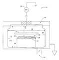
- FIG. 3depicts a cross-sectional view of a parallel plate chemical vapor deposition reactor according to the present invention.
- the present inventiondiscloses an improved method for fabricating a thermally stable ultralow dielectric constant film in a parallel plate plasma enhanced chemical vapor deposition (“PECVD”) reactor.
- the material disclosed in the preferred embodimentcontains a matrix of a hydrogenated oxidized silicon carbon material (SiCOH) comprising Si, C, O and H in a covalently bonded network and having a dielectric constant of not more than about 2.8, which may further contain molecular scale voids, approximately 0.5 to 20 nanometer in diameter, further reducing the dielectric constant to values below about 2.0.
- the dielectric constant for the ultralow-k filmis in a range of about 1.5 to about 2.5, and most preferably the dielectric constant is in a range of about 2.0 to about 2.25.
- the ultralow dielectric constant filmis formed from a mixture of a cyclic siloxane precursor such as TMCTS and a second precursor, which is an organic molecule, selected from the group consisting of molecules with ring structures, such as cyclopentene oxide in the presence of CO 2 or CO 2 and O 2 , in a specifically configured reaction reactor under specific reaction conditions.
- a cyclic siloxane precursorsuch as TMCTS
- a second precursorwhich is an organic molecule, selected from the group consisting of molecules with ring structures, such as cyclopentene oxide in the presence of CO 2 or CO 2 and O 2
- the low dielectric constant film of the present inventioncan further be heat treated at a temperature not less than about 300° C. for at least about 0.25 hour to reduce the dielectric constant.
- molecule fragments derived from the second precursor gas (or gas mixture) comprising carbon and hydrogen and optionally oxygen atomsmay thermally decompose and may be converted into smaller molecules which are released from the film.
- further development of voidsmay occur in the film by the process of conversion and release of the molecule fragments. The film density is thus decreased.
- the present inventionprovides a method for preparing a material that has an ultralow dielectric constant, i.e., lower than about 2.8, which is suitable for integration in a BEOL wiring structure. More preferably, the dielectric constant for the inventive ultralow-k film is in a range of about 1.5 to about 2.5 and, most preferably, the dielectric constant is in a range of about 2.0 to about 2.25.
- the inventive filmscan be prepared by choosing at least two suitable precursors and a specific combination of processing parameters as described herein below.
- the first precursoris selected from molecules with ring structures comprising SiCOH components such as 1,3,5,7-tetramethylcyclotetrasiloxane (TMCTS or C 4 H 16 O 4 Si 4 ) or octamethylcyclotetrasiloxane (OMCTS or C 8 H 24 O 4 Si 4 ).
- TCTS1,3,5,7-tetramethylcyclotetrasiloxane
- OCTSoctamethylcyclotetrasiloxane
- the first precursoris of a class of cyclic alkylsiloxanes comprising a ring structure including an equivalent number of Si and O atoms bonded in an alternating fashion to which alkyl groups (such as methyl, ethyl, propyl or higher or branched analogs as well as cyclic hydrocarbons such as cyclopropyl, cyclopentyl, cyclohexyl, and higher analogs) are covalently bonded to at least one of the silicon atoms, including the cases where all the silicon atoms have two alkyl groups attached. Such alkyl groups may be similar or dissimilar. Additionally, the silicon atoms of such cyclic siloxanes may be bonded to hydrogen, in which case these compounds may be considered partially alkylated hydrosiloxanes.
- alkyl groupssuch as methyl, ethyl, propyl or higher or branched analogs as well as cyclic hydrocarbons such as cyclopropyl, cyclopentyl
- the second precursormay be chosen from organic molecules, containing C, H, and O atoms and containing at least one ring, that have suitable volatility such that they may be introduced to the deposition reactor as a vapor by manipulation of temperature and pressure. Additionally, other atoms such as N, S, Si, or halogens may be contained in the precursor molecule. Additionally, more than one ring may be present in the precursor molecule. Especially useful, are species containing fused rings, at least one of which contains a heteroatom, preferentially oxygen. Of these species, the most suitable are those that include a ring of a size that imparts significant ring strain, namely rings of 3 or 4 atoms and/or 7 or more atoms.
- oxabicyclicsparticularly attractive, are members of a class of compounds known as oxabicyclics.
- species that fit the formula shown in FIG. 1may be considered suitable.
- the first precursoris further mixed with CO 2 as a carrier gas or the first and second precursor gases are mixed with CO 2 or a mixture of CO 2 and O 2 in the PECVD reactor.
- the addition of CO 2 to the first precursor as a carrier gas, or the addition of CO 2 or a mixture of CO 2 and O 2 to the first and second precursors in the PECVD reactorprovides a stabilizing effect on plasma in the PECVD reactor and improves the uniformity of the film deposited on the substrate.
- the amount of CO 2may be from about 25 sccm to about 1000 sccm, and more preferably from about 50 sccm to about 500 sccm.
- the amount of CO 2 admixedmay be from about 25 sccm to about 1000 sccm and the amount of O 2 admixed may be from about 0.5 sccm to 50 sccm. More preferably, the amount of CO 2 is from about 50 sccm to about 500 sccm and the amount of O 2 is from about 1 sccm to about 30 sccm.
- parallel plate plasma enhanced chemical vapor deposition (“PECVD) reactor 10is the type used for processing 200 mm wafers.
- the inner diameter, X, of the reactor 10is approximately 13 inches, while its height, Y, is approximately 8.5 inches.
- the diameter of substrate chuck 12is approximately 10.8 inches.
- Reactant gasesare introduced into reactor 10 through a gas distribution plate (“GDP”) 16 that is spaced apart from substrate chuck 12 by a gap Z of about 1 inch, and are exhausted out of reactor 10 through a 3-inch exhaust port 18 .
- GDPgas distribution plate
- RF power 20is connected to GDP 16 , which is electrically insulated from reactor 10 , and substrate chuck 12 is grounded. For practical purposes, all other parts of the reactor are grounded.
- RF power 20can be connected to substrate chuck 12 and transmitted to substrate 22 .
- the substrateacquires a negative bias, whose value is dependent on the reactor geometry and plasma parameters.
- more than one electrical power supplycan be used.
- two power suppliescan operate at the same RF frequency, or one may operate at a low frequency and one at a high frequency. The two power supplies may be connected both to the same electrode or to separate electrodes.
- the RF power supplycan be pulsed on and off during deposition. Process variables controlled during deposition of the low-k films are RF power, precursor mixture and flow rate, pressure in reactor, and substrate temperature.
- Surfaces 24 of reactor 10may be coated with an insulating coating material. For instance, one specific type of coating is applied on reactor walls 24 to a thickness of several mils.
- Another type of coating material that may be used on substrate chuck 12is a thin coating of alumina or other insulator resistant to etching with an oxygen plasma. The temperature of the heated wafer chuck controls the substrate temperature.
- the inventive ultralow-k material preparedpreferably comprises: between about 5 and about 40 atomic percent of Si; between about 5 and about 45 atomic percent of C; between 0 and about 50 atomic percent of O; and between about 10 and about 55 atomic percent of H.
- the main process variables controlled during a deposition process for a filmare the RF power, the flow rates of the precursors, flow rate of CO 2 , or flow rates of CO 2 and O 2 , the reactor pressure and the substrate temperature.
- the main process variables controlled during a deposition process for a filmare the RF power, the flow rates of the precursors, flow rate of CO 2 , or flow rates of CO 2 and O 2 , the reactor pressure and the substrate temperature.
- TMCTStetramethylcyclotetrasiloxane
- CPOcyclopentene oxide
- the TMCTS precursor vaporswere transported into the reactor by using CO 2 as a carrier gas, while in example 4, the TMCTS precursor was transported by a liquid delivery system.
- the filmswere heat treated at 400° C. after deposition to reduce k.
- the improved fabrication method according to the present inventionis only possible by utilizing a deposition reactor that has a specific geometry with uniquely defined growth conditions.
- the parallel plate reactor according to the present inventionshould have an area of the substrate chuck of between about 300 cm 2 and about 700 cm 2 , and preferably between about 500 cm 2 and about 600 cm 2 .
- the gap between the substrate and the gas distribution plate (or top electrode)is between about 1 cm and about 10 cm, and preferably between about 1.5 cm and about 7 cm.
- a RF poweris applied to one of the electrodes at a frequency between about 12 MHZ and about 15 MHZ, and preferably at about 13.56 MHZ.
- a low frequency, below 1 MHz, powercan optionally be applied at the same electrode as the RF power, or to the opposite electrode at a power density of 0 to 0.3 W/cm 2 .
- the deposition conditions utilizedare also critical to enable a successful implementation of the deposition process according to the present invention.
- a wafer temperatureof between about 25° C. and about 325° C., and preferably of between about 60° C. and about 200° C. is utilized.
- a RF power densitybetween about 0.05 W/cm 2 and about 1.0 W/cm 2 , and preferably between about 0.25 W/cm 2 and about 0.8 W/cm 2 is utilized.
- a reactant gas flow rate of TMCTSbetween about 5 sccm and about 1000 sccm, and preferably between about 25 sccm and about 200 sccm is utilized.
- a reactant gas flow rate of CPObetween about 5 sccm and about 1000 sccm, and preferably between about 10 sccm and about 120 sccm is utilized.
- a total reactant gas flow rate of TMCTS-CO 2where CO 2 is used as a carrier gas is from about 25 sccm to about 1000 sccm, flow rates for CO 2 and O 2 mixture are respectively from about 25 sccm to 1000 sccm for CO 2 and from about 0.5 sccm to about 50 sccm for O 2 , and flow rate for CO 2 from about 15 sccm to about 1000 sccm.
- a total reactant gas flow rate of TMCTS-CO 2where CO 2 is used as a carrier gas is preferably from about 50 sccm to 500 sccm, flow rates for CO 2 and O 2 mixture are preferably respectively from about 50 sccm to about 500 sccm for CO 2 and from about 1 sccm to about 30 sccm for O 2 , and flow rate for CO 2 preferably is from about 50 sccm to about 500 sccm.
- Reactor pressure during the deposition processbetween about 50 mTorr and about 5000 mTorr, and preferably between about 100 mTorr and about 3000 mTorr is utilized.
- a change in the area of the substrate chuck by a factor, Xi.e., a change from a value in the range between about 300 cm 2 and about 700 cm 2
- a change in the area of the substrate chuck by a factor, Yand a change in the gap between the gas distribution plate and the substrate chuck by a factor, Z, from that previously specified, will be associated with a change by a factor, YZ, in the gas flow rates from that previously specified.
- the area of the substraterefers to each individual substrate chuck and the flow rates of the gases refer to one individual deposition station. Accordingly, total flow rates and total power input to the reactor are multiplied by a total number of deposition stations inside the reactor.
- the deposited filmsare stabilized before undergoing further integration processing.
- the stabilization processcan be performed in a furnace-annealing step at about 300° C. to about 400° C. for a time period between about 0.5 hours arid about 4 hours.
- the stabilization processcan also be performed in a rapid thermal annealing process at temperatures above about 300° C.
- the dielectric constants of the films obtained according to the present inventionare lower than about 2.8.
- the thermal stability of the films obtained according to the present invention in non-oxidizing ambientis up to at least a temperature of about 400° C.
- a waferis first prepared by introducing the wafer into reactor 10 through a slit valve 14 and pre-etching the wafer by argon gas.
- the wafer temperatureis set at about 180° C. and the argon flow rate is set at about 25 sccm, to achieve a pressure of about 100 mTorr.
- a RF poweris then turned on to about 125 W for about 60 seconds. The RF power and the argon gas flow are then turned off.
- the TMCTS precursoris carried into the reactor reactor using CO 2 as a carrier gas; CO 2 is at a pressure of about 5 psig at the inlet to the TMCTS container.
- the ultralow-k film according to the present inventioncan be deposited by first establishing gas flows of TMCTS+CO 2 and CPO to desired flow rates and pressure, i.e., at about 20 sccm of TMCTS+CO 2 and about 10 sccm of CPO and about 100 mTorr. A RF power is then turned on at about 15 W for a time period of about 50 minutes. The RF power and the gas flow are then turned off. The wafer is then removed from reaction reactor 10 .
- the filmsare post annealed to evaporate the volatile contents and to dimensionally stabilize the films.
- the post annealing processcan be carried out in an annealing furnace by the following steps. The furnace is first purged for about 5 minutes (with the film samples in a load station) with nitrogen at a flow rate of about 10 liters/minute. The film samples are then transferred into the furnace reactor to start the post annealing cycle of heating the films to about 280° C. at a heating rate of about 5° C./minute, holding at about 280° C.
- a suitable first holding temperaturemay be between about 280° C. and about 300° C., while a suitable second holding temperature may be between about 300° C. and about 400° C.
- a waferis prepared as described in Example 1, but the wafer temperature is set at about 300° C.
- the TMCTS precursoris then carried into the reactor using CO 2 as a carrier gas; CO 2 is at a pressure of about 5 psig at the inlet to the TMCTS container.
- the ultralow-k film according to the present inventioncan be deposited by first establishing gas flows of TMCTS+CO 2 and CPO to desired flow rates and pressure, i.e., at about 150 sccm of TMCTS+CO 2 and about 75 sccm of CPO and about 2000 mTorr.
- a RF poweris then turned on at about 150 W for a time period of about 10 minutes.
- the RF power and the gas floware then turned off.
- the waferis then removed from the reaction reactor 10 and annealed as described in Example 1.
- Example 3the plasma is operated in a pulsed mode.
- the depositionis performed under conditions similar to Example 1, but the plasma is operated in a pulsed mode, i.e., with a duty cycle of about 50% and a plasma-on time of about 50 msec to about 100 msec.
- the wafer with the deposited filmis annealed as described in Example 1.
- a reactor including 6 deposition stationsis used.
- the temperature of the wafer chuckis set at about 350° C.
- the TMCTS precursoris carried into the reactor using a liquid delivery system at a flow rate of about 5 ml/min, the CPO being flown at a rate of about 250 sccm and the pressure being stabilized at about 4000 mTorr.
- the CO 2 at a flow rate of about 5000 sccm and O 2 at a flow rate of about 250 sccmare admixed with the gas mixture of TMCTS and CPO in the reactor.
- the addition of the CO 2 and O 2 mixturestabilizes the plasma and improves the film uniformity.
- a total high frequency RF power of about 600 W and a low frequency RF power of about 300 Ware applied to the reactor.
- the ultralow-k film depositionis performed on the wafer at each station with the wafer moving to the next station after a preset time interval.
- the waferis removed from the reactor after passing the last deposition station, and the wafer may further be optionally annealed as particularly described in Example 1 hereinabove.
- the films that are preparedhave dielectric constants in the range of about 2.0 to about 2.25.
- a rapid thermal annealing (“RTA”) processmay also be used to stabilize ultralow-k films.
- the films obtained according to the present inventionare characterized by dielectric constants k less than about 2.8, and are thermally stable for integration in a back-end-of-the-line (“BEOL”) interconnect structure, which is normally processed at temperatures of up to about 400° C.
- BEOLback-end-of-the-line
- the teachings of the present inventioncan therefore be easily adapted in producing films as intralevel and interlevel dielectrics in back-end-of-the-line processes for logic and memory devices.
Landscapes
- Chemical & Material Sciences (AREA)
- Engineering & Computer Science (AREA)
- Microelectronics & Electronic Packaging (AREA)
- Power Engineering (AREA)
- Condensed Matter Physics & Semiconductors (AREA)
- General Physics & Mathematics (AREA)
- Physics & Mathematics (AREA)
- Computer Hardware Design (AREA)
- Chemical Kinetics & Catalysis (AREA)
- Manufacturing & Machinery (AREA)
- Inorganic Chemistry (AREA)
- General Chemical & Material Sciences (AREA)
- Materials Engineering (AREA)
- Mechanical Engineering (AREA)
- Metallurgy (AREA)
- Organic Chemistry (AREA)
- Formation Of Insulating Films (AREA)
Abstract
Description
Claims (64)
Priority Applications (11)
| Application Number | Priority Date | Filing Date | Title |
|---|---|---|---|
| US09/938,949US6756323B2 (en) | 2001-01-25 | 2001-08-24 | Method for fabricating an ultralow dielectric constant material as an intralevel or interlevel dielectric in a semiconductor device |
| SG200504909-3ASG137694A1 (en) | 2000-10-25 | 2001-10-25 | Ultralow dielectric constant material as an intralevel or interlevel dieletric in a semiconductor device and electronic device containing the same |
| SG200504912-7ASG137695A1 (en) | 2000-10-25 | 2001-10-25 | Method for fabricating an ultralow dielectric constant material as an intralevel or interlevel dieletric in a semiconductor device |
| CNB018204090ACN100386472C (en) | 2000-10-25 | 2001-10-25 | Ultra-low dielectric constant material as intralayer and interlayer insulator in semiconductor device, method of manufacturing same, and electronic device comprising same |
| JP2002544765AJP4272424B2 (en) | 2000-10-25 | 2001-10-25 | Ultralow dielectric constant material as an in-level or inter-level dielectric of a semiconductor element, method for manufacturing the same, and electronic device including the same |
| EP01987525AEP1352107A2 (en) | 2000-10-25 | 2001-10-25 | An ultralow dielectric constant material as an intralevel or interlevel dielectric in a semiconductor device, a method for fabricating the same, and an electronic device containing the same |
| KR1020037005450AKR100586133B1 (en) | 2000-10-25 | 2001-10-25 | Very low dielectric constant materials as in-level or inter-level dielectrics in semiconductor devices, methods for their preparation, and electronic devices containing the materials |
| PCT/US2001/050830WO2002043119A2 (en) | 2000-10-25 | 2001-10-25 | An ultralow dielectric constant material as an intralevel or interlevel dielectric in a semiconductor device, a method for fabricating the same, and an electronic device containing the same |
| US10/174,749US6768200B2 (en) | 2000-10-25 | 2002-06-19 | Ultralow dielectric constant material as an intralevel or interlevel dielectric in a semiconductor device |
| US10/340,000US6770573B2 (en) | 2000-10-25 | 2003-01-10 | Method for fabricating an ultralow dielectric constant material |
| JP2006290010AJP4410783B2 (en) | 2000-10-25 | 2006-10-25 | Method for producing a low dielectric constant film |
Applications Claiming Priority (2)
| Application Number | Priority Date | Filing Date | Title |
|---|---|---|---|
| US09/769,089US6441491B1 (en) | 2000-10-25 | 2001-01-25 | Ultralow dielectric constant material as an intralevel or interlevel dielectric in a semiconductor device and electronic device containing the same |
| US09/938,949US6756323B2 (en) | 2001-01-25 | 2001-08-24 | Method for fabricating an ultralow dielectric constant material as an intralevel or interlevel dielectric in a semiconductor device |
Related Parent Applications (1)
| Application Number | Title | Priority Date | Filing Date |
|---|---|---|---|
| US09/769,089Continuation-In-PartUS6441491B1 (en) | 2000-10-25 | 2001-01-25 | Ultralow dielectric constant material as an intralevel or interlevel dielectric in a semiconductor device and electronic device containing the same |
Related Child Applications (2)
| Application Number | Title | Priority Date | Filing Date |
|---|---|---|---|
| PCT/US2001/050830ContinuationWO2002043119A2 (en) | 2000-10-25 | 2001-10-25 | An ultralow dielectric constant material as an intralevel or interlevel dielectric in a semiconductor device, a method for fabricating the same, and an electronic device containing the same |
| US10/340,000Continuation-In-PartUS6770573B2 (en) | 2000-10-25 | 2003-01-10 | Method for fabricating an ultralow dielectric constant material |
Publications (2)
| Publication Number | Publication Date |
|---|---|
| US20020098714A1 US20020098714A1 (en) | 2002-07-25 |
| US6756323B2true US6756323B2 (en) | 2004-06-29 |
Family
ID=25084421
Family Applications (1)
| Application Number | Title | Priority Date | Filing Date |
|---|---|---|---|
| US09/938,949Expired - LifetimeUS6756323B2 (en) | 2000-10-25 | 2001-08-24 | Method for fabricating an ultralow dielectric constant material as an intralevel or interlevel dielectric in a semiconductor device |
Country Status (1)
| Country | Link |
|---|---|
| US (1) | US6756323B2 (en) |
Cited By (25)
| Publication number | Priority date | Publication date | Assignee | Title |
|---|---|---|---|---|
| US20030211728A1 (en)* | 2000-01-18 | 2003-11-13 | Applied Materials, Inc. | Very low dielectric constant plasma-enhanced CVD films |
| US20040038545A1 (en)* | 1998-02-11 | 2004-02-26 | Applied Materials, Inc. | Plasma processes for depositing low dielectric constant films |
| US20040166665A1 (en)* | 1998-02-11 | 2004-08-26 | Applied Materials, Inc. | Method of decreasing the K value in SIOC layer deposited by chemical vapor deposition |
| US20040175581A1 (en)* | 2003-03-03 | 2004-09-09 | Applied Materials, Inc. | Modulated/composited CVD low-k films with improved mechanical and electrical properties for nanoelectronic devices |
| US20050059264A1 (en)* | 1998-09-29 | 2005-03-17 | David Cheung | CVD plasma assisted low dielectric constant films |
| US6890850B2 (en) | 2001-12-14 | 2005-05-10 | Applied Materials, Inc. | Method of depositing dielectric materials in damascene applications |
| US20050130440A1 (en)* | 2001-12-14 | 2005-06-16 | Yim Kang S. | Low dielectric (low k) barrier films with oxygen doping by plasma-enhanced chemical vapor deposition (PECVD) |
| US20050215065A1 (en)* | 2004-03-23 | 2005-09-29 | Applied Materials, Inc. | Low dielectric constant porous films |
| US20050276930A1 (en)* | 2003-03-18 | 2005-12-15 | International Business Machines Corporation | Ultra low K (ULK) SiCOH film and method |
| US20060063012A1 (en)* | 2004-08-30 | 2006-03-23 | Samsung Corning Co., Ltd. | Method for preparing low dielectric constant film by using dual organic siloxane precursor |
| US7030041B2 (en) | 2004-03-15 | 2006-04-18 | Applied Materials Inc. | Adhesion improvement for low k dielectrics |
| US20060183345A1 (en)* | 2005-02-16 | 2006-08-17 | International Business Machines Corporation | Advanced low dielectric constant organosilicon plasma chemical vapor deposition films |
| US20070057234A1 (en)* | 2005-09-12 | 2007-03-15 | Fujifilm Electronic Materials U.S.A., Inc. | Additives to prevent degradation of cyclic alkene derivatives |
| US20070057235A1 (en)* | 2005-09-12 | 2007-03-15 | Fujifilm Electronic Materials U.S.A., Inc. | Additives to prevent degradation of cyclic alkene derivatives |
| US20070148966A1 (en)* | 2005-12-22 | 2007-06-28 | Baks Heidi L | Method of forming an interconnect structure |
| US20090093130A1 (en)* | 2002-10-30 | 2009-04-09 | Fujitsu Limited | Silicon oxycarbide, growth method of silicon oxycarbide layer, semiconductor device and manufacture method for semiconductor device |
| US20090127669A1 (en)* | 2007-09-18 | 2009-05-21 | Nec Corporation | Method for forming interlayer dielectric film, interlayer dielectric film, semiconductor device and semiconductor manufacturing apparatus |
| US20090291210A1 (en)* | 2005-09-12 | 2009-11-26 | Fujifilm Electronic Materials U.S.A., Inc. | Additives to Prevent Degradation of Cyclic Alkene Derivatives |
| EP2141141A1 (en) | 2008-05-28 | 2010-01-06 | Air Products and Chemicals, Inc. | Improved Process Stability of NBDE Using Substituted Phenol Stabilizers |
| US20100052115A1 (en)* | 2008-09-03 | 2010-03-04 | American Air Liquide, Inc. | Volatile Precursors for Deposition of C-Linked SiCOH Dielectrics |
| US20100143580A1 (en)* | 2008-05-28 | 2010-06-10 | American Air Liquide, Inc. | Stabilization of Bicycloheptadiene |
| US20100233829A1 (en)* | 2009-03-10 | 2010-09-16 | American Air Liquide Inc. | Cyclic amino compounds for low-k silylation |
| EP2319821A1 (en) | 2009-11-06 | 2011-05-11 | L'Air Liquide Société Anonyme pour l'Etude et l'Exploitation des Procédés Georges Claude | Stabilization of bicycloheptadiene |
| WO2011103282A2 (en) | 2010-02-17 | 2011-08-25 | L'air Liquide, Societe Anonyme Pour L'etude Et L'exploitation Des Procedes Georges Claude | VAPOR DEPOSITION METHODS OF SiCOH LOW-K FILMS |
| US20120252227A1 (en)* | 2002-10-30 | 2012-10-04 | Fujitsu Semiconductor Limited | Silicon oxycarbide, growth method of silicon oxycarbide layer, semiconductor device and manufacture method for semiconductor device |
Families Citing this family (27)
| Publication number | Priority date | Publication date | Assignee | Title |
|---|---|---|---|---|
| US6303523B2 (en)* | 1998-02-11 | 2001-10-16 | Applied Materials, Inc. | Plasma processes for depositing low dielectric constant films |
| US6593247B1 (en) | 1998-02-11 | 2003-07-15 | Applied Materials, Inc. | Method of depositing low k films using an oxidizing plasma |
| US6287990B1 (en) | 1998-02-11 | 2001-09-11 | Applied Materials, Inc. | CVD plasma assisted low dielectric constant films |
| US6054379A (en) | 1998-02-11 | 2000-04-25 | Applied Materials, Inc. | Method of depositing a low k dielectric with organo silane |
| EP1352107A2 (en)* | 2000-10-25 | 2003-10-15 | International Business Machines Corporation | An ultralow dielectric constant material as an intralevel or interlevel dielectric in a semiconductor device, a method for fabricating the same, and an electronic device containing the same |
| US6531398B1 (en) | 2000-10-30 | 2003-03-11 | Applied Materials, Inc. | Method of depositing organosillicate layers |
| US6683346B2 (en)* | 2001-03-09 | 2004-01-27 | Fairchild Semiconductor Corporation | Ultra dense trench-gated power-device with the reduced drain-source feedback capacitance and Miller charge |
| US6777171B2 (en) | 2001-04-20 | 2004-08-17 | Applied Materials, Inc. | Fluorine-containing layers for damascene structures |
| US6486082B1 (en)* | 2001-06-18 | 2002-11-26 | Applied Materials, Inc. | CVD plasma assisted lower dielectric constant sicoh film |
| US6936309B2 (en)* | 2002-04-02 | 2005-08-30 | Applied Materials, Inc. | Hardness improvement of silicon carboxy films |
| US20030194495A1 (en)* | 2002-04-11 | 2003-10-16 | Applied Materials, Inc. | Crosslink cyclo-siloxane compound with linear bridging group to form ultra low k dielectric |
| US20030211244A1 (en)* | 2002-04-11 | 2003-11-13 | Applied Materials, Inc. | Reacting an organosilicon compound with an oxidizing gas to form an ultra low k dielectric |
| US20030194496A1 (en)* | 2002-04-11 | 2003-10-16 | Applied Materials, Inc. | Methods for depositing dielectric material |
| US6815373B2 (en)* | 2002-04-16 | 2004-11-09 | Applied Materials Inc. | Use of cyclic siloxanes for hardness improvement of low k dielectric films |
| US7060330B2 (en)* | 2002-05-08 | 2006-06-13 | Applied Materials, Inc. | Method for forming ultra low k films using electron beam |
| US6936551B2 (en)* | 2002-05-08 | 2005-08-30 | Applied Materials Inc. | Methods and apparatus for E-beam treatment used to fabricate integrated circuit devices |
| US7056560B2 (en)* | 2002-05-08 | 2006-06-06 | Applies Materials Inc. | Ultra low dielectric materials based on hybrid system of linear silicon precursor and organic porogen by plasma-enhanced chemical vapor deposition (PECVD) |
| US7105460B2 (en)* | 2002-07-11 | 2006-09-12 | Applied Materials | Nitrogen-free dielectric anti-reflective coating and hardmask |
| US6927178B2 (en)* | 2002-07-11 | 2005-08-09 | Applied Materials, Inc. | Nitrogen-free dielectric anti-reflective coating and hardmask |
| TWI273090B (en)* | 2002-09-09 | 2007-02-11 | Mitsui Chemicals Inc | Method for modifying porous film, modified porous film and use of same |
| US6897163B2 (en) | 2003-01-31 | 2005-05-24 | Applied Materials, Inc. | Method for depositing a low dielectric constant film |
| US6913992B2 (en) | 2003-03-07 | 2005-07-05 | Applied Materials, Inc. | Method of modifying interlayer adhesion |
| US20050214457A1 (en)* | 2004-03-29 | 2005-09-29 | Applied Materials, Inc. | Deposition of low dielectric constant films by N2O addition |
| US7288205B2 (en) | 2004-07-09 | 2007-10-30 | Applied Materials, Inc. | Hermetic low dielectric constant layer for barrier applications |
| US7381659B2 (en)* | 2005-11-22 | 2008-06-03 | International Business Machines Corporation | Method for reducing film stress for SiCOH low-k dielectric materials |
| US20070134435A1 (en)* | 2005-12-13 | 2007-06-14 | Ahn Sang H | Method to improve the ashing/wet etch damage resistance and integration stability of low dielectric constant films |
| US7297376B1 (en) | 2006-07-07 | 2007-11-20 | Applied Materials, Inc. | Method to reduce gas-phase reactions in a PECVD process with silicon and organic precursors to deposit defect-free initial layers |
- 2001
- 2001-08-24USUS09/938,949patent/US6756323B2/ennot_activeExpired - Lifetime
Cited By (73)
| Publication number | Priority date | Publication date | Assignee | Title |
|---|---|---|---|---|
| US7074708B2 (en) | 1998-02-11 | 2006-07-11 | Applied Materials, Inc. | Method of decreasing the k value in sioc layer deposited by chemical vapor deposition |
| US20040038545A1 (en)* | 1998-02-11 | 2004-02-26 | Applied Materials, Inc. | Plasma processes for depositing low dielectric constant films |
| US20040166665A1 (en)* | 1998-02-11 | 2004-08-26 | Applied Materials, Inc. | Method of decreasing the K value in SIOC layer deposited by chemical vapor deposition |
| US6930061B2 (en) | 1998-02-11 | 2005-08-16 | Applied Materials Inc. | Plasma processes for depositing low dielectric constant films |
| US7205249B2 (en) | 1998-09-29 | 2007-04-17 | Applied Materials, Inc. | CVD plasma assisted low dielectric constant films |
| US20050059264A1 (en)* | 1998-09-29 | 2005-03-17 | David Cheung | CVD plasma assisted low dielectric constant films |
| US7012030B2 (en) | 2000-01-18 | 2006-03-14 | Applied Materials Inc. | Very low dielectric constant plasma-enhanced CVD films |
| US20040235291A1 (en)* | 2000-01-18 | 2004-11-25 | Mandal Robert P. | Very low dielectric constant plasma-enhanced CVD films |
| US20050136240A1 (en)* | 2000-01-18 | 2005-06-23 | Mandal Robert P. | Very low dielectric constant plasma-enhanced CVD films |
| US20030211728A1 (en)* | 2000-01-18 | 2003-11-13 | Applied Materials, Inc. | Very low dielectric constant plasma-enhanced CVD films |
| US20060226548A1 (en)* | 2000-01-18 | 2006-10-12 | Mandal Robert P | Very low dielectric constant plasma-enhanced cvd films |
| US7094710B2 (en) | 2000-01-18 | 2006-08-22 | Applied Materials | Very low dielectric constant plasma-enhanced CVD films |
| US7399697B2 (en) | 2000-01-18 | 2008-07-15 | Applied Materials, Inc. | Very low dielectric constant plasma-enhanced CVD films |
| US7205224B2 (en) | 2000-01-18 | 2007-04-17 | Applied Materials, Inc. | Very low dielectric constant plasma-enhanced CVD films |
| US7825042B2 (en) | 2000-01-18 | 2010-11-02 | Applied Materials, Inc. | Very low dielectric constant plasma-enhanced CVD films |
| US7633163B2 (en) | 2000-01-18 | 2009-12-15 | Applied Materials, Inc. | Very low dielectric constant plasma-enhanced CVD films |
| US7601631B2 (en) | 2000-01-18 | 2009-10-13 | Appplied Materials, Inc. | Very low dielectric constant plasma-enhanced CVD films |
| US6890850B2 (en) | 2001-12-14 | 2005-05-10 | Applied Materials, Inc. | Method of depositing dielectric materials in damascene applications |
| US20090053902A1 (en)* | 2001-12-14 | 2009-02-26 | Kang Sub Yim | Low dielectric (low k) barrier films with oxygen doping by plasma-enhanced chemical vapor deposition (pecvd) |
| US20050130440A1 (en)* | 2001-12-14 | 2005-06-16 | Yim Kang S. | Low dielectric (low k) barrier films with oxygen doping by plasma-enhanced chemical vapor deposition (PECVD) |
| US20050233576A1 (en)* | 2001-12-14 | 2005-10-20 | Lee Ju-Hyung | Method of depositing dielectric materials in damascene applications |
| US7745328B2 (en) | 2001-12-14 | 2010-06-29 | Applied Materials, Inc. | Low dielectric (low k) barrier films with oxygen doping by plasma-enhanced chemical vapor deposition (PECVD) |
| US20060246737A1 (en)* | 2001-12-14 | 2006-11-02 | Yim Kang S | New low dielectric (low k) barrier films with oxygen doping by plasma-enhanced chemical vapor deposition (pecvd) |
| US7151053B2 (en) | 2001-12-14 | 2006-12-19 | Applied Materials, Inc. | Method of depositing dielectric materials including oxygen-doped silicon carbide in damascene applications |
| US7157384B2 (en) | 2001-12-14 | 2007-01-02 | Applied Materials, Inc. | Low dielectric (low k) barrier films with oxygen doping by plasma-enhanced chemical vapor deposition (PECVD) |
| US7465659B2 (en) | 2001-12-14 | 2008-12-16 | Applied Materials, Inc. | Low dielectric (low k) barrier films with oxygen doping by plasma-enhanced chemical vapor deposition (PECVD) |
| US8349722B2 (en)* | 2002-10-30 | 2013-01-08 | Fujitsu Semiconductor Limited | Silicon oxycarbide, growth method of silicon oxycarbide layer, semiconductor device and manufacture method for semiconductor device |
| US20090093130A1 (en)* | 2002-10-30 | 2009-04-09 | Fujitsu Limited | Silicon oxycarbide, growth method of silicon oxycarbide layer, semiconductor device and manufacture method for semiconductor device |
| US20120252227A1 (en)* | 2002-10-30 | 2012-10-04 | Fujitsu Semiconductor Limited | Silicon oxycarbide, growth method of silicon oxycarbide layer, semiconductor device and manufacture method for semiconductor device |
| US8778814B2 (en)* | 2002-10-30 | 2014-07-15 | Fujitsu Semiconductor Limited | Silicon oxycarbide, growth method of silicon oxycarbide layer, semiconductor device and manufacture method for semiconductor device |
| US7011890B2 (en) | 2003-03-03 | 2006-03-14 | Applied Materials Inc. | Modulated/composited CVD low-k films with improved mechanical and electrical properties for nanoelectronic devices |
| US20040175581A1 (en)* | 2003-03-03 | 2004-09-09 | Applied Materials, Inc. | Modulated/composited CVD low-k films with improved mechanical and electrical properties for nanoelectronic devices |
| US20090297823A1 (en)* | 2003-03-18 | 2009-12-03 | International Business Machines Corporation | ULTRA LOW K (ULK) SiCOH FILM AND METHOD |
| US20050276930A1 (en)* | 2003-03-18 | 2005-12-15 | International Business Machines Corporation | Ultra low K (ULK) SiCOH film and method |
| US7288292B2 (en)* | 2003-03-18 | 2007-10-30 | International Business Machines Corporation | Ultra low k (ULK) SiCOH film and method |
| US20080026203A1 (en)* | 2003-03-18 | 2008-01-31 | International Business Machines Corporation | ULTRA LOW K (ULK) SiCOH FILM AND METHOD |
| US7459404B2 (en) | 2004-03-15 | 2008-12-02 | Applied Materials, Inc. | Adhesion improvement for low k dielectrics |
| US7030041B2 (en) | 2004-03-15 | 2006-04-18 | Applied Materials Inc. | Adhesion improvement for low k dielectrics |
| US20050215065A1 (en)* | 2004-03-23 | 2005-09-29 | Applied Materials, Inc. | Low dielectric constant porous films |
| US7060638B2 (en) | 2004-03-23 | 2006-06-13 | Applied Materials | Method of forming low dielectric constant porous films |
| US20060063012A1 (en)* | 2004-08-30 | 2006-03-23 | Samsung Corning Co., Ltd. | Method for preparing low dielectric constant film by using dual organic siloxane precursor |
| US20070128882A1 (en)* | 2005-02-16 | 2007-06-07 | International Business Machines Corporation | Advanced low dielectric constant organosilicon plasma chemical vapor deposition films |
| US7202564B2 (en) | 2005-02-16 | 2007-04-10 | International Business Machines Corporation | Advanced low dielectric constant organosilicon plasma chemical vapor deposition films |
| US7494938B2 (en) | 2005-02-16 | 2009-02-24 | International Business Machines Corporation | Advanced low dielectric constant organosilicon plasma chemical vapor deposition films |
| US20060183345A1 (en)* | 2005-02-16 | 2006-08-17 | International Business Machines Corporation | Advanced low dielectric constant organosilicon plasma chemical vapor deposition films |
| US20090291210A1 (en)* | 2005-09-12 | 2009-11-26 | Fujifilm Electronic Materials U.S.A., Inc. | Additives to Prevent Degradation of Cyclic Alkene Derivatives |
| US20070057234A1 (en)* | 2005-09-12 | 2007-03-15 | Fujifilm Electronic Materials U.S.A., Inc. | Additives to prevent degradation of cyclic alkene derivatives |
| US20070057235A1 (en)* | 2005-09-12 | 2007-03-15 | Fujifilm Electronic Materials U.S.A., Inc. | Additives to prevent degradation of cyclic alkene derivatives |
| US8252704B2 (en) | 2005-09-12 | 2012-08-28 | Fujifilm Electronic Materials U.S.A., Inc. | Additives to prevent degradation of cyclic alkene derivatives |
| US7985350B2 (en) | 2005-09-12 | 2011-07-26 | Fujifilm Electronic Materials U.S.A., Inc. | Additives to prevent degradation of cyclic alkene derivatives |
| US7931823B2 (en) | 2005-09-12 | 2011-04-26 | Fujifilm Electronic Materials U.S.A., Inc. | Additives to prevent degradation of cyclic alkene derivatives |
| US7883639B2 (en) | 2005-09-12 | 2011-02-08 | Fujifilm Electronic Materials, U.S.A., Inc. | Additives to prevent degradation of cyclic alkene derivatives |
| WO2007033123A2 (en) | 2005-09-12 | 2007-03-22 | Fujifilm Electronic Materials U.S.A., Inc. | Additives to prevent degradation of cyclic alkene derivatives |
| US7871536B2 (en) | 2005-09-12 | 2011-01-18 | Fujifilm Electronic Materials U.S.A., Inc. | Additives to prevent degradation of cyclic alkene derivatives |
| US7358182B2 (en) | 2005-12-22 | 2008-04-15 | International Business Machines Corporation | Method of forming an interconnect structure |
| US20070148966A1 (en)* | 2005-12-22 | 2007-06-28 | Baks Heidi L | Method of forming an interconnect structure |
| US20080146029A1 (en)* | 2005-12-22 | 2008-06-19 | Heidi Lee Baks | Method of forming an interconnect structure |
| US20090127669A1 (en)* | 2007-09-18 | 2009-05-21 | Nec Corporation | Method for forming interlayer dielectric film, interlayer dielectric film, semiconductor device and semiconductor manufacturing apparatus |
| US8598706B2 (en)* | 2007-09-18 | 2013-12-03 | Renesas Electronics Corporation | Method for forming interlayer dielectric film, interlayer dielectric film, semiconductor device and semiconductor manufacturing apparatus |
| US8173213B2 (en) | 2008-05-28 | 2012-05-08 | Air Products And Chemicals, Inc. | Process stability of NBDE using substituted phenol stabilizers |
| EP3141538A1 (en) | 2008-05-28 | 2017-03-15 | Air Products And Chemicals, Inc. | Improved process stability of nbde using substituted phenol stabilizers |
| US20100143580A1 (en)* | 2008-05-28 | 2010-06-10 | American Air Liquide, Inc. | Stabilization of Bicycloheptadiene |
| EP2141141A1 (en) | 2008-05-28 | 2010-01-06 | Air Products and Chemicals, Inc. | Improved Process Stability of NBDE Using Substituted Phenol Stabilizers |
| WO2010005937A1 (en) | 2008-07-08 | 2010-01-14 | Fujifilm Electronic Materials U.S.A., Inc. | Additives to prevent degradation of cyclic alkene derivatives |
| US8298965B2 (en) | 2008-09-03 | 2012-10-30 | American Air Liquide, Inc. | Volatile precursors for deposition of C-linked SiCOH dielectrics |
| US20100052115A1 (en)* | 2008-09-03 | 2010-03-04 | American Air Liquide, Inc. | Volatile Precursors for Deposition of C-Linked SiCOH Dielectrics |
| WO2010104979A2 (en) | 2009-03-10 | 2010-09-16 | L'air Liquide - Société Anonyme Pour L'Étude Et L'exploitation Des Procédes Georges Claude | Cyclic amino compounds for low-k silylation |
| US20100233829A1 (en)* | 2009-03-10 | 2010-09-16 | American Air Liquide Inc. | Cyclic amino compounds for low-k silylation |
| US8999734B2 (en) | 2009-03-10 | 2015-04-07 | American Air Liquide, Inc. | Cyclic amino compounds for low-k silylation |
| EP2319821A1 (en) | 2009-11-06 | 2011-05-11 | L'Air Liquide Société Anonyme pour l'Etude et l'Exploitation des Procédés Georges Claude | Stabilization of bicycloheptadiene |
| WO2011054713A1 (en) | 2009-11-06 | 2011-05-12 | L'air Liquide Societe Anonyme Pour L'etude Et L'exploitation Des Procedes Georges Claude | Stabilization of bicycloheptadiene |
| US8932674B2 (en) | 2010-02-17 | 2015-01-13 | American Air Liquide, Inc. | Vapor deposition methods of SiCOH low-k films |
| WO2011103282A2 (en) | 2010-02-17 | 2011-08-25 | L'air Liquide, Societe Anonyme Pour L'etude Et L'exploitation Des Procedes Georges Claude | VAPOR DEPOSITION METHODS OF SiCOH LOW-K FILMS |
Also Published As
| Publication number | Publication date |
|---|---|
| US20020098714A1 (en) | 2002-07-25 |
Similar Documents
| Publication | Publication Date | Title |
|---|---|---|
| US6756323B2 (en) | Method for fabricating an ultralow dielectric constant material as an intralevel or interlevel dielectric in a semiconductor device | |
| US6770573B2 (en) | Method for fabricating an ultralow dielectric constant material | |
| US6541398B2 (en) | Ultralow dielectric constant material as an intralevel or interlevel dielectric in a semiconductor device and electronic device containing the same | |
| US6768200B2 (en) | Ultralow dielectric constant material as an intralevel or interlevel dielectric in a semiconductor device | |
| US6790789B2 (en) | Ultralow dielectric constant material as an intralevel or interlevel dielectric in a semiconductor device and electronic device made | |
| US7049247B2 (en) | Method for fabricating an ultralow dielectric constant material as an intralevel or interlevel dielectric in a semiconductor device and electronic device made | |
| EP1617957B1 (en) | Method of forming an ultra low dielectric constant film | |
| CN100400707C (en) | Method for hardening low dielectric constant film by electron beam | |
| US7354873B2 (en) | Method for forming insulation film | |
| US7282458B2 (en) | Low K and ultra low K SiCOH dielectric films and methods to form the same | |
| TW563202B (en) | An ultralow dielectric constant material as an intralevel or interlevel dielectric in a semiconductor device and an electronic device containing the same |
Legal Events
| Date | Code | Title | Description |
|---|---|---|---|
| AS | Assignment | Owner name:INTERNATIONAL BUSINESS MACHINES CORPORATION, NEW Y Free format text:ASSIGNMENT OF ASSIGNORS INTEREST;ASSIGNORS:GRILL ALFRED;PATEL, VISHNUBHAI V.;REEL/FRAME:012122/0563 Effective date:20010823 | |
| FEPP | Fee payment procedure | Free format text:PAYOR NUMBER ASSIGNED (ORIGINAL EVENT CODE: ASPN); ENTITY STATUS OF PATENT OWNER: LARGE ENTITY | |
| STCF | Information on status: patent grant | Free format text:PATENTED CASE | |
| FPAY | Fee payment | Year of fee payment:4 | |
| FPAY | Fee payment | Year of fee payment:8 | |
| FEPP | Fee payment procedure | Free format text:PAYER NUMBER DE-ASSIGNED (ORIGINAL EVENT CODE: RMPN); ENTITY STATUS OF PATENT OWNER: LARGE ENTITY Free format text:PAYOR NUMBER ASSIGNED (ORIGINAL EVENT CODE: ASPN); ENTITY STATUS OF PATENT OWNER: LARGE ENTITY | |
| AS | Assignment | Owner name:INTEL CORPORATION, CALIFORNIA Free format text:ASSIGNMENT OF ASSIGNORS INTEREST;ASSIGNOR:INTERNATIONAL BUSINESS MACHINES CORPORATION;REEL/FRAME:031940/0056 Effective date:20131028 | |
| FPAY | Fee payment | Year of fee payment:12 |