US6754108B2 - DRAM cells with repressed floating gate memory, low tunnel barrier interpoly insulators - Google Patents
DRAM cells with repressed floating gate memory, low tunnel barrier interpoly insulatorsDownload PDFInfo
- Publication number
- US6754108B2 US6754108B2US09/945,395US94539501AUS6754108B2US 6754108 B2US6754108 B2US 6754108B2US 94539501 AUS94539501 AUS 94539501AUS 6754108 B2US6754108 B2US 6754108B2
- Authority
- US
- United States
- Prior art keywords
- floating gate
- gate
- tunnel barrier
- control gate
- source
- Prior art date
- Legal status (The legal status is an assumption and is not a legal conclusion. Google has not performed a legal analysis and makes no representation as to the accuracy of the status listed.)
- Expired - Lifetime
Links
- 230000015654memoryEffects0.000titleclaimsabstractdescription194
- 238000007667floatingMethods0.000titleclaimsabstractdescription152
- 230000004888barrier functionEffects0.000titleclaimsabstractdescription122
- 239000012212insulatorSubstances0.000titleclaimsabstractdescription112
- 238000000034methodMethods0.000claimsabstractdescription52
- 239000003990capacitorSubstances0.000claimsabstractdescription44
- 238000003860storageMethods0.000claimsabstractdescription38
- 239000000758substrateSubstances0.000claimsabstractdescription37
- 229910052751metalInorganic materials0.000claimsdescription67
- 239000002184metalSubstances0.000claimsdescription67
- 229910021420polycrystalline siliconInorganic materials0.000claimsdescription48
- 230000005641tunnelingEffects0.000claimsdescription33
- TWNQGVIAIRXVLR-UHFFFAOYSA-Noxo(oxoalumanyloxy)alumaneChemical compoundO=[Al]O[Al]=OTWNQGVIAIRXVLR-UHFFFAOYSA-N0.000claimsdescription32
- 229920005591polysiliconPolymers0.000claimsdescription29
- ZKATWMILCYLAPD-UHFFFAOYSA-Nniobium pentoxideChemical compoundO=[Nb](=O)O[Nb](=O)=OZKATWMILCYLAPD-UHFFFAOYSA-N0.000claimsdescription28
- 150000004706metal oxidesChemical class0.000claimsdescription27
- GWEVSGVZZGPLCZ-UHFFFAOYSA-NTitan oxideChemical compoundO=[Ti]=OGWEVSGVZZGPLCZ-UHFFFAOYSA-N0.000claimsdescription26
- MCMNRKCIXSYSNV-UHFFFAOYSA-NZirconium dioxideChemical compoundO=[Zr]=OMCMNRKCIXSYSNV-UHFFFAOYSA-N0.000claimsdescription26
- HTUMBQDCCIXGCV-UHFFFAOYSA-Nlead oxideChemical compound[O-2].[Pb+2]HTUMBQDCCIXGCV-UHFFFAOYSA-N0.000claimsdescription25
- 229910044991metal oxideInorganic materials0.000claimsdescription25
- PBCFLUZVCVVTBY-UHFFFAOYSA-Ntantalum pentoxideInorganic materialsO=[Ta](=O)O[Ta](=O)=OPBCFLUZVCVVTBY-UHFFFAOYSA-N0.000claimsdescription14
- 239000002784hot electronSubstances0.000claimsdescription11
- 229910000314transition metal oxideInorganic materials0.000claimsdescription11
- 238000002347injectionMethods0.000claimsdescription9
- 239000007924injectionSubstances0.000claimsdescription9
- 229910052782aluminiumInorganic materials0.000claimsdescription8
- XAGFODPZIPBFFR-UHFFFAOYSA-NaluminiumChemical compound[Al]XAGFODPZIPBFFR-UHFFFAOYSA-N0.000claimsdescription8
- 229910052723transition metalInorganic materials0.000claimsdescription3
- 150000003624transition metalsChemical class0.000claimsdescription3
- 108091006146ChannelsProteins0.000claims20
- 210000000746body regionAnatomy0.000claims11
- YEXPOXQUZXUXJW-UHFFFAOYSA-NoxoleadChemical compound[Pb]=OYEXPOXQUZXUXJW-UHFFFAOYSA-N0.000claims3
- 102000004129N-Type Calcium ChannelsHuman genes0.000claims1
- 108090000699N-Type Calcium ChannelsProteins0.000claims1
- 210000004027cellAnatomy0.000description93
- 239000010408filmSubstances0.000description41
- 238000012546transferMethods0.000description36
- 239000010410layerSubstances0.000description30
- 230000003647oxidationEffects0.000description28
- 238000007254oxidation reactionMethods0.000description28
- 230000005684electric fieldEffects0.000description21
- VYPSYNLAJGMNEJ-UHFFFAOYSA-NSilicium dioxideChemical compoundO=[Si]=OVYPSYNLAJGMNEJ-UHFFFAOYSA-N0.000description13
- QVGXLLKOCUKJST-UHFFFAOYSA-Natomic oxygenChemical compound[O]QVGXLLKOCUKJST-UHFFFAOYSA-N0.000description12
- 229910052760oxygenInorganic materials0.000description12
- 239000001301oxygenSubstances0.000description12
- 230000015572biosynthetic processEffects0.000description11
- 238000010586diagramMethods0.000description11
- 150000002739metalsChemical class0.000description11
- 230000008569processEffects0.000description11
- 230000000694effectsEffects0.000description9
- 238000012545processingMethods0.000description9
- 230000004044responseEffects0.000description8
- 229910045601alloyInorganic materials0.000description7
- 239000000956alloySubstances0.000description7
- 238000013459approachMethods0.000description7
- 239000000203mixtureSubstances0.000description7
- 239000004065semiconductorSubstances0.000description7
- 229910052814silicon oxideInorganic materials0.000description7
- 230000015556catabolic processEffects0.000description6
- 238000011065in-situ storageMethods0.000description6
- 230000002028prematureEffects0.000description6
- 230000006870functionEffects0.000description5
- 238000004519manufacturing processMethods0.000description5
- 238000005259measurementMethods0.000description5
- 238000002488metal-organic chemical vapour depositionMethods0.000description5
- 238000011282treatmentMethods0.000description5
- XUIMIQQOPSSXEZ-UHFFFAOYSA-NSiliconChemical compound[Si]XUIMIQQOPSSXEZ-UHFFFAOYSA-N0.000description4
- 238000000151depositionMethods0.000description4
- 230000008018meltingEffects0.000description4
- 238000002844meltingMethods0.000description4
- 230000006386memory functionEffects0.000description4
- 230000001590oxidative effectEffects0.000description4
- 229910052710siliconInorganic materials0.000description4
- 239000010703siliconSubstances0.000description4
- SJHPCNCNNSSLPL-CSKARUKUSA-N(4e)-4-(ethoxymethylidene)-2-phenyl-1,3-oxazol-5-oneChemical compoundO1C(=O)C(=C/OCC)\N=C1C1=CC=CC=C1SJHPCNCNNSSLPL-CSKARUKUSA-N0.000description3
- 230000008901benefitEffects0.000description3
- 238000013461designMethods0.000description3
- 238000009792diffusion processMethods0.000description3
- 239000000463materialSubstances0.000description3
- RJCRUVXAWQRZKQ-UHFFFAOYSA-Noxosilicon;siliconChemical compound[Si].[Si]=ORJCRUVXAWQRZKQ-UHFFFAOYSA-N0.000description3
- 238000001552radio frequency sputter depositionMethods0.000description3
- 239000000377silicon dioxideSubstances0.000description3
- 238000004544sputter depositionMethods0.000description3
- MYMOFIZGZYHOMD-UHFFFAOYSA-NDioxygenChemical compoundO=OMYMOFIZGZYHOMD-UHFFFAOYSA-N0.000description2
- 230000002411adverseEffects0.000description2
- 230000008859changeEffects0.000description2
- 238000004891communicationMethods0.000description2
- 230000007547defectEffects0.000description2
- 239000003989dielectric materialSubstances0.000description2
- 229910001882dioxygenInorganic materials0.000description2
- 238000005516engineering processMethods0.000description2
- 239000012535impuritySubstances0.000description2
- 239000011261inert gasSubstances0.000description2
- 230000003993interactionEffects0.000description2
- 239000013641positive controlSubstances0.000description2
- 230000009257reactivityEffects0.000description2
- 238000001953recrystallisationMethods0.000description2
- 229910021332silicideInorganic materials0.000description2
- FVBUAEGBCNSCDD-UHFFFAOYSA-Nsilicide(4-)Chemical compound[Si-4]FVBUAEGBCNSCDD-UHFFFAOYSA-N0.000description2
- 235000012239silicon dioxideNutrition0.000description2
- 238000000992sputter etchingMethods0.000description2
- 239000000126substanceSubstances0.000description2
- 239000010409thin filmSubstances0.000description2
- OKTJSMMVPCPJKN-UHFFFAOYSA-NCarbonChemical compound[C]OKTJSMMVPCPJKN-UHFFFAOYSA-N0.000description1
- 229910000881Cu alloyInorganic materials0.000description1
- 102100037807GATOR complex protein MIOSHuman genes0.000description1
- 101000950705Homo sapiens GATOR complex protein MIOSProteins0.000description1
- 241000013355Mycteroperca interstitialisSpecies0.000description1
- 229910052581Si3N4Inorganic materials0.000description1
- 230000003213activating effectEffects0.000description1
- 239000012080ambient airSubstances0.000description1
- 238000003491arrayMethods0.000description1
- 230000006399behaviorEffects0.000description1
- 230000009286beneficial effectEffects0.000description1
- 229910052799carbonInorganic materials0.000description1
- 210000003850cellular structureAnatomy0.000description1
- 238000004140cleaningMethods0.000description1
- 229910052681coesiteInorganic materials0.000description1
- 239000002131composite materialSubstances0.000description1
- 238000004883computer applicationMethods0.000description1
- 229910052906cristobaliteInorganic materials0.000description1
- 239000013078crystalSubstances0.000description1
- 230000008021depositionEffects0.000description1
- 238000001514detection methodMethods0.000description1
- 238000000572ellipsometryMethods0.000description1
- 230000008020evaporationEffects0.000description1
- 238000001704evaporationMethods0.000description1
- 238000011066ex-situ storageMethods0.000description1
- 230000005669field effectEffects0.000description1
- 238000007496glass formingMethods0.000description1
- 230000006872improvementEffects0.000description1
- 230000000977initiatory effectEffects0.000description1
- 239000011810insulating materialSubstances0.000description1
- 150000002500ionsChemical class0.000description1
- WABPQHHGFIMREM-UHFFFAOYSA-Nlead(0)Chemical compound[Pb]WABPQHHGFIMREM-UHFFFAOYSA-N0.000description1
- 238000012417linear regressionMethods0.000description1
- 239000011159matrix materialSubstances0.000description1
- 150000002736metal compoundsChemical class0.000description1
- 239000007769metal materialSubstances0.000description1
- 238000001465metallisationMethods0.000description1
- 238000012986modificationMethods0.000description1
- 230000004048modificationEffects0.000description1
- 229910052758niobiumInorganic materials0.000description1
- 150000004767nitridesChemical class0.000description1
- 229910000510noble metalInorganic materials0.000description1
- 229910052763palladiumInorganic materials0.000description1
- 230000037361pathwayEffects0.000description1
- 230000002093peripheral effectEffects0.000description1
- 229910052697platinumInorganic materials0.000description1
- 238000004886process controlMethods0.000description1
- HQVNEWCFYHHQES-UHFFFAOYSA-Nsilicon nitrideChemical compoundN12[Si]34N5[Si]62N3[Si]51N64HQVNEWCFYHHQES-UHFFFAOYSA-N0.000description1
- 239000002356single layerSubstances0.000description1
- 239000000243solutionSubstances0.000description1
- 230000003068static effectEffects0.000description1
- 229910052682stishoviteInorganic materials0.000description1
- 210000000352storage cellAnatomy0.000description1
- 229910052715tantalumInorganic materials0.000description1
- 238000007669thermal treatmentMethods0.000description1
- 229910052905tridymiteInorganic materials0.000description1
- 229910052727yttriumInorganic materials0.000description1
Images


Classifications
- H—ELECTRICITY
- H10—SEMICONDUCTOR DEVICES; ELECTRIC SOLID-STATE DEVICES NOT OTHERWISE PROVIDED FOR
- H10D—INORGANIC ELECTRIC SEMICONDUCTOR DEVICES
- H10D30/00—Field-effect transistors [FET]
- H10D30/60—Insulated-gate field-effect transistors [IGFET]
- H10D30/68—Floating-gate IGFETs
- H10D30/681—Floating-gate IGFETs having only two programming levels
- G—PHYSICS
- G11—INFORMATION STORAGE
- G11C—STATIC STORES
- G11C11/00—Digital stores characterised by the use of particular electric or magnetic storage elements; Storage elements therefor
- G11C11/21—Digital stores characterised by the use of particular electric or magnetic storage elements; Storage elements therefor using electric elements
- G11C11/34—Digital stores characterised by the use of particular electric or magnetic storage elements; Storage elements therefor using electric elements using semiconductor devices
- G11C11/40—Digital stores characterised by the use of particular electric or magnetic storage elements; Storage elements therefor using electric elements using semiconductor devices using transistors
- G11C11/401—Digital stores characterised by the use of particular electric or magnetic storage elements; Storage elements therefor using electric elements using semiconductor devices using transistors forming cells needing refreshing or charge regeneration, i.e. dynamic cells
- G11C11/403—Digital stores characterised by the use of particular electric or magnetic storage elements; Storage elements therefor using electric elements using semiconductor devices using transistors forming cells needing refreshing or charge regeneration, i.e. dynamic cells with charge regeneration common to a multiplicity of memory cells, i.e. external refresh
- G11C11/404—Digital stores characterised by the use of particular electric or magnetic storage elements; Storage elements therefor using electric elements using semiconductor devices using transistors forming cells needing refreshing or charge regeneration, i.e. dynamic cells with charge regeneration common to a multiplicity of memory cells, i.e. external refresh with one charge-transfer gate, e.g. MOS transistor, per cell
- H—ELECTRICITY
- H10—SEMICONDUCTOR DEVICES; ELECTRIC SOLID-STATE DEVICES NOT OTHERWISE PROVIDED FOR
- H10B—ELECTRONIC MEMORY DEVICES
- H10B12/00—Dynamic random access memory [DRAM] devices
- H10B12/01—Manufacture or treatment
- H10B12/02—Manufacture or treatment for one transistor one-capacitor [1T-1C] memory cells
- H10B12/05—Making the transistor
- H—ELECTRICITY
- H10—SEMICONDUCTOR DEVICES; ELECTRIC SOLID-STATE DEVICES NOT OTHERWISE PROVIDED FOR
- H10D—INORGANIC ELECTRIC SEMICONDUCTOR DEVICES
- H10D30/00—Field-effect transistors [FET]
- H10D30/60—Insulated-gate field-effect transistors [IGFET]
- H10D30/68—Floating-gate IGFETs
- H10D30/6891—Floating-gate IGFETs characterised by the shapes, relative sizes or dispositions of the floating gate electrode
- H—ELECTRICITY
- H10—SEMICONDUCTOR DEVICES; ELECTRIC SOLID-STATE DEVICES NOT OTHERWISE PROVIDED FOR
- H10D—INORGANIC ELECTRIC SEMICONDUCTOR DEVICES
- H10D64/00—Electrodes of devices having potential barriers
- H10D64/60—Electrodes characterised by their materials
- H10D64/66—Electrodes having a conductor capacitively coupled to a semiconductor by an insulator, e.g. MIS electrodes
- H10D64/68—Electrodes having a conductor capacitively coupled to a semiconductor by an insulator, e.g. MIS electrodes characterised by the insulator, e.g. by the gate insulator
- H10D64/681—Electrodes having a conductor capacitively coupled to a semiconductor by an insulator, e.g. MIS electrodes characterised by the insulator, e.g. by the gate insulator having a compositional variation, e.g. multilayered
Definitions
- the present inventionrelates generally to integrated circuits, and in particular to DRAM cells with repressed floating gate memory, metal oxide tunnel interpoly insulators.
- An essential semiconductor deviceis semiconductor memory, such as a random access memory (RAM) device.
- RAMrandom access memory
- a RAM deviceallows the user to execute both read and write operations on its memory cells.
- Typical examples of RAM devicesinclude dynamic random access memory (DRAM) and static random access memory (SRAM).
- DRAMis a specific category of RAM containing an array of individual memory cells, where each cell includes a capacitor for holding a charge and a transistor for accessing the charge held in the capacitor.
- the transistoris often referred to as the access transistor or the transfer device of the DRAM cell.
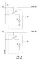
- FIG. 1illustrates a portion of a DRAM memory circuit containing two neighboring DRAM cells 100 .
- Each cell 100contains a storage capacitor 140 and an access field effect transistor or transfer device 120 .
- one side of the storage capacitor 140is connected to a reference voltage (illustrated as a ground potential for convenience purposes).
- the other side of the storage capacitor 140is connected to the drain of the transfer device 120 .
- the gate of the transfer device 120is connected to a signal known in the art as a word line 180 .
- the source of the transfer device 120is connected to a signal known in the art as a bit line 160 (also known in the art as a digit line).
- each cell 100contains one bit of data (i.e., a logic “0” or logic “1”).
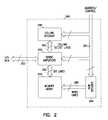
- the DRAM 240contains a memory array 242 , row and column decoders 244 , 248 and a sense amplifier circuit 246 .
- the memory array 242consists of a plurality of memory cells 200 (constructed as illustrated in FIG. 1) whose word lines 280 and bit lines 260 are commonly arranged into rows and columns, respectively.
- the bit lines 260 of the memory array 242are connected to the sense amplifier circuit 246 , while its word lines 280 are connected to the row decoder 244 .
- Address and control signalsare input on address/control lines 261 into the DRAM 240 and connected to the column decoder 248 , sense amplifier circuit 246 and row decoder 244 and are used to gain read and write access, among other things, to the memory array 242 .
- the column decoder 248is connected to the sense amplifier circuit 246 via control and column select signals on column select lines 262 .
- the sense amplifier circuit 246receives input data destined for the memory array 242 and outputs data read from the memory array 242 over input/output ( 1 / 0 ) data lines 263 .
- Datais read from the cells of the memory array 242 by activating a word line 280 (via the row decoder 244 ), which couples all of the memory cells corresponding to that word line to respective bit lines 260 , which define the columns of the array.
- One or more bit lines 260are also activated.
- the sense amplifier circuit 246 connected to a bit line columndetects and amplifies the data bit transferred from the storage capacitor of the memory cell to its bit line 260 by measuring the potential difference between the activated bit line 260 and a reference line which may be an inactive bit line.
- a reference linewhich may be an inactive bit line.
- DRAM devicesare the most cost effective high speed memory used with computers and computer systems. They last (nearly) indefinitely and are available in very high density. They are, however, limited in the longevity of their memory. DRAM devices require constant refreshing and lose all knowledge of their state (i.e., contents) once power to the device is removed. It is desirable to have a memory device, such as a DRAM memory device, with all of the positive features of DRAM devices, e.g., cost, size, speed, availability, etc., that retains its memory state when power is removed from the device.
- a DRAM cell with a nonvolatile componentwould be very beneficial in numerous computer systems and computer applications.
- One applicationwould be the saving and/or restoring of the state of a central processing unit (CPU) that is executing software instructions in a protected mode of operation, an example of which is disclosed in U.S. Pat. No. 5,497,494 to Combs et al., which is hereby incorporated by reference in its entirety.
- This applicationtypically involves the use of memory separate from the main memory of the computer, typically referred to as shadow RAM, from which a BIOS program is executed and the CPU state is to be stored to and retrieved from. This, however, consumes valuable chip real estate.
- a main memorycontains data and error detection codes associated with each piece of data.
- a separate shadow memoryis used to store data corresponding to the data stored in the main memory. If the system determines that accessed data from the main memory is erroneous, the corresponding data from the shadow memory is used and thus, faults in the main memory do not adversely effect the system (i.e., the system is fault tolerant). Again, memory separate from the main memory is required, which adds cost and adds to the size and complexity of the system.
- Flash memoryis another form of non-volatile memory. Flash memories have become widely accepted in a variety of applications ranging from personal computers, to digital cameras and wireless phones. Both INTEL and AMD have separately each produced about one billion integrated circuit chips in this technology.
- any such memory cellsshould avoid the added cost, size and complexity of having separate volatile and nonvolatile memory cell components.
- the non-volatile memory componentshould avoid the large barriers to electron tunneling or hot electron injection presented by the silicon oxide-silicon interface, 3.2 eV, which result in slow write and erase speeds even at very high electric fields.
- the above mentioned problems with conventional memories and other problemsare addressed by the present invention and will be understood by reading and studying the following specification.
- Systems and methodsare provided for high density memories having both a volatile and non-volatile component.
- the nonvolatile componentincludes a floating gate separated from a control gate by a metal oxide and/or low tunnel barrier interpoly insulator.
- memory cells having a volatile and a non-volatile component in a single cellare provided.
- the memory cellincludes a first source/drain region and a second source/drain region separated by a channel region in a substrate.
- a storage capacitoris coupled to one of the first and the second source/drain regions.
- a floating gateopposes the channel region and separated therefrom by a gate oxide.
- a control gateopposes the floating gate. The control gate is separated from the floating gate by a low tunnel barrier intergate insulator.
- the memory cellis adapted to operate in a first and a second mode of operation. The first mode of operation is a dynamic mode of operation and the second mode of operation is a repressed memory mode of operation.
- FIG. 1is a circuit diagram illustrating conventional dynamic random access memory (DRAM) cells.
- DRAMdynamic random access memory
- FIG. 2is a block diagram illustrating a DRAM device.
- FIGS. 3A and 3Bare circuit diagrams illustrating DRAM cells constructed in accordance with different embodiments of the present invention.
- FIG. 4is a block diagram of a memory device such as can include DRAM cells constructed in accordance with the embodiments of the present invention.
- FIG. 5illustrates an exemplary process for sensing the state of the nonvolatile memory component of the DRAM cells illustrated in FIGS. 3A and 3B.
- FIGS. 6A and 6Billustrate a sense amplifier voltage response over time associated with the sensing of the contents of the DRAM cells illustrated in FIGS. 3A and 3B.
- FIG. 7Ais an energy band diagram illustrating the band structure at vacuum level with the low tunnel barrier interpoly insulator according to the teachings of the present invention.
- FIG. 7Bis an energy band diagram illustrating the band structure during an erase operation of electrons from the floating gate to the control gate across the low tunnel barrier interpoly insulator according to the teachings of the present invention.
- FIG. 7Cis a graph plotting tunneling currents versus the applied electric fields (reciprocal applied electric field shown) for an number of barrier heights.
- FIG. 8illustrates a block diagram of a computer system utilizing the DRAM cells illustrated in FIGS. 3A and 3B.
- wafer and substrateare interchangeably used to refer generally to any structure on which integrated circuits are formed, and also to such structures during various stages of integrated circuit fabrication. Both terms include doped and undoped semiconductors, epitaxial layers of a semiconductor on a supporting semiconductor or insulating material, combinations of such layers, as well as other such structures that are known in the art.
- horizontalas used in this application is defined as a plane parallel to the conventional plane or surface of a wafer or substrate, regardless of the orientation of the wafer or substrate.
- verticalrefers to a direction perpendicular to the horizonal as defined above.
- Prepositions, such as “on”, “side” (as in “sidewall”), “higher”, “lower”, “over” and “under”are defined with respect to the conventional plane or surface being on the top surface of the wafer or substrate, regardless of the orientation of the wafer or substrate.
- the present inventiondescribes the use of a memory cell having a volatile and a non-volatile memory component.
- the non-volatile memory componentincludes a metal oxide inter-poly dielectric insulators between the control gate and the floating gate.
- An exampleis shown in FIG. 3A for a planar structure, or horizontal memory cell. According to the teachings of the present invention.
- the use of metal oxide films for this purposeoffer a number of advantages including:
- FIG. 3Aillustrates one embodiment of a memory cell 300 , according to the teachings of the present invention.
- the memory cell 300includes a first source/drain region 318 and a second source/drain region 322 separated by a channel region 321 in a substrate 320 .
- a floating gate 316opposes the channel region 321 and is separated therefrom by a gate oxide 326 .
- a control gate 314opposes the floating gate 316 .
- the control gate 314is separated from the floating gate 316 by a low tunnel barrier intergate insulator 324 .
- low tunnel barrier intergate insulator 324includes a metal oxide insulator selected from the group consisting of lead oxide (PbO) and aluminum oxide (Al 2 O 3 ).
- the low tunnel barrier intergate insulator 324includes a transition metal oxide and the transition metal oxide is selected from the group consisting of Ta 2 O 5 , TiO 2 , ZrO 2 , and Nb 2 O 5 .
- the low tunnel barrier intergate insulator 324includes a Perovskite oxide tunnel barrier.
- the floating gate 316includes a polysilicon floating gate 316 having a metal layer 371 formed thereon in contact with the low tunnel barrier intergate insulator 324 .
- the control gate 314includes a polysilicon control gate 314 having a metal layer 372 formed thereon in contact with the low tunnel barrier intergate insulator 324 .
- the metal layers, 371 and 372are formed of the same metal material used to form the metal oxide interpoly insulator 324 .
- FIG. 3Billustrates another embodiment of a memory cell 300 , according to the teachings of the present invention.
- a first source/drain region 318 and a second source/drain region 322are separated by a channel region 321 in a substrate.
- a storage capacitor 340is coupled to one of the first and the second source/drain regions, 318 and 322 .
- a floating gate 316opposes the channel region 321 and is separated therefrom by a gate oxide 321 .
- a vertical, edge defined control gate 314opposes the floating gate 316 , wherein the vertical control gate 314 is separated from the floating gate 316 by a low tunnel barrier intergate insulator 324 .
- the memory cell 300is controllable to access a first charge representing a data value from the storage capacitor 340 in a first mode of operation and a second charge representing a data value from the floating gate 316 in a second mode of operation.
- the first chargeis accessible without affecting the second charge and the second charge is accessible without affecting the first charge.
- the low tunnel barrier intergate insulator 324includes a metal oxide insulator 324 selected from the group consisting of PbO, Al 2 O 3 , Ta 2 O 5 , TiO 2 , ZrO 2 , Nb 2 O 5 .
- the low tunnel barrier intergate insulator 324includes a Perovskite oxide tunnel barrier.
- the floating gate 316includes a polysilicon floating gate 316 having a metal layer 371 formed thereon in contact with the low tunnel barrier intergate insulator 324 .
- the vertical, edge defined control gate 314includes a vertical, edge defined polysilicon control gate 314 having a metal layer 372 formed thereon in contact with the low tunnel barrier intergate insulator 324 .
- FIGS. 3A and 3Bare circuit diagrams illustrating DRAM cells 300 constructed in accordance with an embodiment of the present invention.
- the cells 300are similar to the cells 100 illustrated in FIG. 1 with the exception that a different transfer device 312 replaces the transfer device 112 shown in FIG. 1 .
- the transfer device 312is a transistor having a control gate 314 and an additional gate 316 , often referred to as a floating gate, and is of the kind often used in flash memory devices.
- the transfer device 312has a drain 318 connected to one end of the storage capacitor 340 and a source 322 connected to the bit line 360 (as in the conventional DRAM cell 100 illustrated in FIG. 1 ).
- the source 322 and drain 318are constructed from a N+ type region of high impurity concentration formed on a P-type semiconductor substrate 320 and are separated by a channel region 321 .
- the memory cell of the present inventionincludes both a volatile and non-volatile memory component.
- the non-volatile componentincludes a floating gate 316 which is isolated from the control gate 314 by a low tunnel barrier intergate insulator 324 and from the source 322 , drain 318 and channel 321 by a gate oxide 326 .
- the low tunnel barrier intergate insulator 324includes an intergate insulator 324 selected from the group consisting of PbO, Al 2 O 3 , Ta 2 O 5 , TiO 2 , ZrO 2 , Nb 2 O 5 .
- the low tunnel barrier intergate insulator 324includes a Perovskite oxide tunnel barrier.
- the floating gate 316includes a polysilicon floating gate 316 having a metal layer 371 formed thereon in contact with the low tunnel barrier intergate insulator 324 .
- control gate 314includes a polysilicon control gate 314 having a metal layer 372 formed thereon in contact with the low tunnel barrier intergate insulator 324 .
- the use of the transfer device 312allows the cell 300 of the present invention to be operated as either a conventional DRAM cell or as a nonvolatile memory cell (herein referred to as a DRAM with “repressed memory”).
- the DRAM portioni.e., the storage capacitor 340
- all that is requiredis to place a large positive voltage onto the control gate 314 via the word line 380 and the data from the bit line 360 will be transferred to the capacitor 340 .
- the floating gate 316may contain a charge on it. This charge may slightly alter the characteristics (e.g., resistance) of the transfer device 312 .
- the transfer of information to/from the bit line 360may be slower in the cell 300 of the present invention when compared to a similar transfer in the conventional DRAM cell 100 illustrated in FIG. 1 .
- a tunnel—tunnel mode of operationwill be used to program one of two different charge states onto the floating gate 316 and thus, program the transfer device 312 into one of two states.
- a tunnel modeis used to transfer electrons from the source 322 to the floating gate 316 to program the transfer device 312 , e.g. the floating gate 316 and thus the nonvolatile portion of the cell 300 , to a first charge state.
- This first charge stateis referred to herein as the tunnel write operation. That is, write can be achieved by the normal channel hot electron injection and gate current through the gate silicon oxide 326 to the floating gate 316 .
- writecan also be accomplished by applying a positive voltage to the substrate or well select line and a large negative voltage to the control gates 314 , electrons will tunnel from the control gate 314 to the floating gate 316 .
- the low tunnel barrier 324will provide an easy write operation and the selection of the substrate or well bias will provide selectivity and address only one device.
- a negative charge on the floating gate 316can be associated with either a logic “0” or “1” and that the invention is not limited to any particular association between the first charge state and a particular logic value.
- the one requirementis that the program, erase and sensing circuitry used to access the nonvolatile portion of the cell 300 associate the first charge state to the same logic value.
- a tunnel modeis used to transfer the electrons from the floating gate 316 to the control gate 314 to program the transfer device 312 , e.g. the floating gate 316 and thus the nonvolatile portion of the cell 300 , to a second charge state.
- the second charge stateis referred to herein as the tunnel erase operation.
- the tunnel erase operationis achieved by driving the floating gate 316 , through the control gate 314 and word line 380 , with a large positive voltage. That is, according to the teachings of the present invention, erase is achieved by providing a negative voltage to the substrate or well address line and a large positive voltage to the control gate 314 . This causes electrons to tunnel off of the floating gate 316 on to the control gate 314 .
- a whole rowcan be erased by addressing all the column lines along that row and a block can be erased by addressing multiple row back gate or substrate/well address lines.
- a column lineis addressed by applying a positive control gate voltage and the current sensed along the data bit or drain row address line. Different currents will result in different read times.
- the lack of a negative charge on the floating gate 316can be associated with either a logic “0” or “1” and that the invention is not limited to any particular association between the second charge state and a particular logic value.
- the one requirementis that the program, erase and sensing circuitry used to access the nonvolatile portion of the cell 300 associate the second charge state to the same logic value and that the logic value be different than the value chosen for the first charge state.
- FIG. 4is a block diagram of a memory device such as can include DRAM cells constructed in accordance with the embodiments of the present invention.
- memory cells 300 of either embodiment shown in FIGS. 3A and 3Bare embedded in an array of similar cells as shown in FIG. 4.
- a typical memory arrayconsists of a matrix of storage bits with bit capacity 2 N ⁇ 2 M bits arranged in an array 475 with 2 M columns (bit lines) and 2 N rows (word lines).
- a row addressis input and decoded by row decoder 480 to select one of the rows or word lines. All of the cells along this word line are activated.
- Column decoder 482then addresses one bit out of the 2 M bits that have been activated and routes the data that is stored in that bit to a sense amplifier (not shown) and then out of the array 475 . Data in and Data out are controlled by the Read/Write Control circuit 484 .
- FIG. 5is a flow chart illustrate the manner in which information is read/sensed from a DRAM cell having repressed memory according to the teachings of the present invention. Initially it must be determined whether the DRAM cell with repressed memory is being accessed as a DRAM or as a nonvolatile memory. This is shown in FIG. 5 as decision step 502 . If the DRAM cell having repressed memory is to be operated as a DRAM, a voltage in excess of the normal threshold voltage of the cell's transfer device is applied to the control gate of the cell, 510 . A charge on the floating gate may effect the characteristics (e.g., resistance) of the transfer device and its threshold voltage.
- a voltage in excess of the normal threshold voltage of the cell's transfer deviceis applied to the control gate of the cell, 510 .
- a charge on the floating gatemay effect the characteristics (e.g., resistance) of the transfer device and its threshold voltage.
- a difference in threshold voltage of the transfer devicewill have no effect on the potential transferred to the bit line, but it will effect the rate at which it is transferred.
- the difference in threshold voltage and resistance of the transfer devicedetermines only the current, but the DRAM sense amplifiers respond only to potential differences.
- the word linemay be driven to a voltage as far as possible in excess of the threshold voltage of the transfer device to minimize the resistance of the transfer device (typically a few thousand ohms). This results in the charge stored in the capacitor being transferred to the bit line in a sub-nanosecond time period.
- the sense amplifiersubsequently responds with either a sensed Vout + or a Vout ⁇ , depending upon the charge stored in the capacitor, after time t S whether or not the floating gate is in the first charge state, 512 . Once the sense amplifier has sensed the potential on the bit line, the appropriate data value may be output, 508 .
- a voltage that is approximately equal to the typical threshold voltage of the cell transfer deviceis applied to the control gate of the cell, 504 . This will cause the charge stored on the capacitor to be transferred to the bit line. This charge is not being used for its data value since it represents the stored DRAM value. Instead, as will be described below, the charge is being used to determine the response time of the sense amplifier, since the response time is indicative of whether the transfer device is programmed to the first or second charge state, 506 .
- a charge on the floating gatemay effect the characteristics, e.g. resistance, of the transfer device and its threshold voltage.
- the characteristicswill vary depending upon the threshold voltage. For example, if the threshold voltage is high, e.g. 0.6 volts, the transfer device has a higher resistance and it will not conduct well. This would represent the case when electrons are stored on the floating gate. That is, the floating gate is programmed to the first charge state. Likewise, if the threshold voltage is low, e.g. 0.0 volts, the transfer device has a low resistance and it will conduct much better. This would represent the case when electrons are not stored on the floating gate. That is, the floating gate is programmed to the second charge state.
- the resistance of the transfer devicecan be sensed.
- the resistancewill determine the response time of the sense amplifier.
- FIG. 6Ais a graph of the sense amp voltage response versus time for the DRAM cell having repressed memory, according to the teachings of the present invention, when the non-volatile memory portion of the cell, is in an unprogrammed state. That is, the floating gate is programmed to the second charge state. If the transfer device has a low resistance because it has been programmed with the second charge state, the stored charge from the storage capacitor (whose value is not important) is transferred to the bit line at approximately the same speed as the transfer of the charge described in steps 510 and 512 , e.g. DRAM operation. The sense amplifier subsequently responds with, for example, a sensed Vout ⁇ after time t S as shown in FIG. 6 A. It should be appreciated that the second charge state can be associated with a sensed Vout + instead of the Vout ⁇ .
- FIG. 6Bis a graph of the sense amp voltage response versus time for the DRAM cell having repressed memory, according to the teachings of the present invention, when the non-volatile memory portion of the cell is in a programmed state. That is, the floating gate is programmed to the first charge state having electrons stored thereon. If the transfer device has a high resistance because it has been programmed to the first charge state the stored charge from the storage capacitor, whose value is not important, is transferred to the bit line much slower in comparison to the transfer of the charge described in steps 510 and 512 , e.g. DRAM operation. As shown in FIG.
- the sense amplifierwhen a stored charge is present on the floating gate (first charge state) the sense amplifier subsequently responds with, for example, a sensed Vout + after time t S + ⁇ t. It should be appreciated that the first charge state can be associated with a sensed Vout ⁇ instead of the Vout + .
- the appropriate data valuemay be output, 508 .
- the DRAM cell 300 of the present inventioncan be operated as a DRAM and a nonvolatile memory and is suitable for use in many applications and systems that require both DRAM and nonvolatile memory. Examples include a fault tolerant system, start-up conditions, the saving and/or restoring of the state of a central processing unit (CPU) that is executing software instructions in a protected mode of operation, and shadow memory applications.
- the cell 300can be used in an array such as the array 242 within the DRAM device 240 illustrated in FIG. 2 or it can be used as a separate special purpose memory if so desired.
- a DRAM devicesuch as the device 240 illustrated in FIG. 2 can contain an array 242 having conventional DRAM cells and DRAM cells with repressed memory constructed in accordance with the present invention.
- the decision when to access the cell 300 as a DRAM and when to access it as a nonvolatile memoryis application specific. For example, data can be written into the DRAM portion of the cell 300 and copied to the nonvolatile portion. Similarly, data can be written into the nonvolatile portion and then copied in to the DRAM portion. It is also possible to operate the DRAM and nonvolatile portions independently of each other. Any of these methods can be used and the invention is not to be limited to any particular method of using the DRAM and nonvolatile portions of the cell 300 .
- FIG. 7Ashows the band structure of the silicon substrate, e.g. channel region 701 , silicon dioxide gate insulator, e.g. gate oxide 703 , polysilicon floating gate 705 , the low tunnel barrier interpoly dielectric 707 , between metal plates 709 and 711 , and then the polysilicon control gate 713 , according to the teachings of the present invention.
- the design considerations involvedare determined by the dielectric constant, thickness and tunneling barrier height of the interpoly dielectric insulator 707 relative to that of the silicon dioxide gate insulator, e.g. gate oxide 703 .
- the tunneling probability through the interpoly dielectric 707is an exponential function of both the barrier height and the electric field across this dielectric.
- FIG. 7Bis an energy band diagram illustrating the band structure during an erase operation of electrons from the floating gate 705 to the control gate 713 across the low tunnel barrier interpoly insulator 707 according to the teachings of the present invention.
- FIG. 7Bis similarly useful in illustrating the reduced tunnel barrier off of the floating gate 705 to the control gate 713 and for illustrating the respective capacitances of the structure in the non-volatile memory component according to the teachings of the present invention.
- the electric fieldis determined by the total voltage difference across the structure, the ratio of the capacitances (see FIG. 7 A), and the thickness of the interpoly dielectric 707 .
- Eis the electric field across the interpoly dielectric insulator 707 and Eo depends on the barrier height, ⁇ 0 .
- the lower electric field in the aluminum oxide interpoly insulator 707 for the same current densityreflects the lower tunneling barrier of less than 2 eV, shown in FIG. 7B, as opposed to the 3.2 eV tunneling barrier of silicon oxide 703 , also illustrated in FIG. 7 B.
- FIG. 7Cis a graph plotting tunneling currents versus the applied electric fields (reciprocal applied electric field shown) for a number of barrier heights.
- FIG. 7Cillustrates the dependence of the tunneling currents in the non-volatile memory component on electric field (reciprocal applied electric field) and barrier height.
- the fraction of voltage across the interpoly or intergate insulator, ⁇ V 2can be increased by making the area of the intergate capacitor, C 2 , (e.g. intergate insulator 707 ) smaller than the area of the transistor gate capacitor, C 1 (e.g. gate oxide 703 ). This would be required with high dielectric constant intergate dielectric insulators 707 and is easily realized with the control gate structure described above in connection with FIG. 3 B.
- the poly-Si layeris to be formed with emphasis on obtaining a surface that is very smooth and morphologically stable at subsequent device processing temperatures which will exceed that used to grow Metal oxide.
- the native SiO x oxide on the poly-Si surfacemust be removed (e.g., by sputter cleaning in an inert gas plasma in situ) just prior to depositing the metal film.
- the electrical characteristics of the resultant Poly-Si/Metal/Metal oxide/Metal/Poly-Si structurewill be better defined and reproducible than that of a Poly-Si/Native SiO x /Metal/Metal oxide/Poly-Si structure.
- the oxide growth rate and limiting thicknesswill increase with oxidation temperature and oxygen pressure.
- the oxidation kinetics of a metalmay, in some cases, depend on the crystallographic orientations of the very small grains of metal which comprise the metal film. If such effects are significant, the metal deposition process can be modified in order to increase its preferred orientation and subsequent oxide thickness and tunneling uniformity. To this end, use can be made of the fact that metal films strongly prefer to grow during their depositions having their lowest free energy planes parallel to the film surface. This preference varies with the crystal structure of the metal. For example, fcc metals prefer to form ⁇ 111 ⁇ surface plans. Metal orientation effects, if present, would be larger when only a limited fraction of the metal will be oxidized and unimportant when all or most of the metal is oxidized.
- Modifications in the structure shown in FIG. 2may be introduced in order to compensate for certain properties in some metal/oxide/metal layers. Such changes are reasonable since a wide range of metals, alloys and oxides with quite different physical and chemical properties can be used to form these tunnel junctions.
- Lead and other metal filmscan be deposited by various means including physical sputtering and/or from a Knudsen evaporation cell.
- the sputtering processalso offers the ability to produce smoother films by increasing the re-sputtering-to-deposition ratio since re-sputtering preferentially reduces geometric high points of the film.
- Matisooentitled “Measurement of tunnel current density in a Meal-Oxide-Metal system as a function of oxide thickness.”
- This remarkable degree of control over tunnel currentis due to the excellent control over PbO thickness that can be achieved by “low temperature oxidation.”
- increasing the oxidation time from 100 to 1,000 minutes at an oxygen pressure of 750 Torr at 25Conly raises the PbO thickness by 3 A.
- controlling the oxidation time to within 1 out of a nominal 100 minute total oxidation timeprovides a thickness that is within 0.1 A of 21A.
- the PbOhas a highly stoichiometric composition throughout its thickness, as evidenced from ellipsometry and the fact that the tunnel barrier heights are identical for Pb/PbO/Pb structures.
- the temperature used to subsequently deposit the Poly-Si control gatemust be held below the melting temperature (327C) of lead.
- the PbOitself is stable (up to ⁇ 500C or higher) and thus introduces no temperature constraint on subsequent processes.
- Yet another variation out of severalwould involve: oxidizing the lead film to completion; replacing the top lead electrode with a higher melting metal such as Al; and, then adding the poly-Si control layer. This junction would have asymmetrical tunneling behavior due to the difference in barrier heights between the Pb/PbO and PbO/Al electrodes.
- Tunnel currentsare asymmetrical in this system with somewhat larger currents flowing when electrons are injected from Al/Al 2 O 3 interface developed during oxide growth. This asymmetry is due to a minor change in composition of the growing oxide: there is a small concentration of excess metal in the Al 2 O 3 , the concentration of which diminishes as the oxide is grown thicker. The excess Al +3 ions produce a space charge that lowers the tunnel barrier at the inner interface. The oxide composition at the outer Al 2 O 3 /Al contact is much more stoichiometric and thus has a higher tunnel barrier. In situ ellipsometer measurements on the thermal oxidation of Al films deposited and oxidized in situ support this model.
- Al/Al 2 O 3 /Al tunnel barrierscan be formed that will produce predictable and highly controllable tunnel currents that can be ejected from either electrode.
- the magnitude of the currentsare still primarily dominated by Al 2 O 3 thickness which can be controlled via the oxidation parametrics.
- Al 2 O 3 tunnel barrierswe can proceed to outline one process path out of several that can be used to form Al 2 O 3 tunnel barriers.
- the aluminumis thermally oxidized although one could use other techniques such as plasma oxidation or rf sputtering in an oxygen plasma.
- plasma oxidation or rf sputtering in an oxygen plasmaFor the sake of brevity, some details noted above will not be repeated.
- the formation of the Al/Al 2 O 3 /Al structureswill be seen to be simpler than that described for the Pb/PbO/Pb junctions owing to the much higher melting point of aluminum, relative to lead.
- Single layers of Ta 2 O 5 , TiO 2 , ZrO 2 , Nb 2 O 5 and similar transition metal oxidescan be formed by “low temperature oxidation” of numerous Transition Metal (e.g., TM oxides) films in molecular and plasma oxygen and also by rf sputtering in an oxygen plasma.
- TM oxidesTransition Metal
- the thermal oxidation kinetics of these metalshave been studied for decades with numerous descriptions and references. In essence, such metals oxidize via logarithmic kinetics to reach thicknesses of a few to several tens of angstroms in the range of 100 to 300C.
- Excellent oxide barriers for Josephson tunnel devicescan be formed by rf sputter etching these metals in an oxygen plasma.
- MOCVD filmsrequire high temperature oxidation treatments to remove carbon impurities, improve oxide stoichiometry and produce recrystallization. Such high temperature treatments also cause unwanted interactions between the oxide and the underlying silicon and thus have necessitated the introduction of interfacial barrier layers.
- this treatmentcan be carried out in an inert gas atmosphere, thus lessening the possibility of inadvertently oxidizing the poly-Si floating gate.
- This earlier disclosurewas directed at developing methods and procedures for producing high dielectric constant films for storage cells for DRAMs, the same teachings can be applied to producing thinner metal oxide tunnel films for the flash memory devices described in this disclosure.
- the dielectric constants of these TM oxidesare substantially greater (>25 to 30 or more) than those of PbO and Al 2 O 3 .
- Duplex layers of these high dielectric constant oxide filmsare easily fabricated with simple tools and also provide improvement in device yields and reliability. Each oxide layer will contain some level of defects but the probability that such defects will overlap is exceedingly small.
- Thinner TM layerswill be used in this invention relative to those used to form DRAMs. Unlike DRAMs where leakage must be eliminated, the duplex oxides used here must be thin enough to carry very controlled levels of current flow when subjected to reasonable applied fields and times.
- TM and their oxidesare highly refractory and etchable (e.g., by RIE). Hence they are quite compatible with poly-Si control gate processes and other subsequent steps.
- a stack of oxide filmshaving quite different properties, for example, a stack comprised of a high dielectric constant (k) oxide/a low k oxide/a high k oxide.
- Low temperature oxidationcan be used to form numerous variations of such structures. While most of this disclosure deals with the formation and use of stacks of oxide dielectrics, it is also possible to use “low temperature oxidation” to form other thin film dielectrics such as nitrides, oxynitrides, etc. that could provide additional functions such as being altered by monochromatic light, etc. These will not be discussed further here.
- the TM layerswould typically be pure metals although they could be alloyed.
- the TMsare similar metallurgically as are their oxides.
- the parent alloy films that can be converted to a perovskite oxideare typically comprised of metals having widely different chemical reactivities with oxygen and other common gasses.
- Y—Ba—Cu systemreferenced above, Y and Ba are among the most reactive of metals while the reactivity of Cu approaches (albeit distantly) those of other noble metals. If the alloy is to be completely oxidized, then thin film barriers such as Pd, Pt, etc. or their conductive oxides must be added between the Si and the parent metal film to serve as: electrical contact layers; diffusion barriers; and, oxidation stops.
- the Schottky barrier heights of various TM oxides and perovskite oxides in contact with various metalswill help in the design of the tunnel device.
- the barrier heightswill represent that developed during oxide growth at the parent perovskite alloy/perovskite oxide interface.
- barrier heightscannot be predicted ab initio for such a wide class of materials but will have to be developed as the need arises. This information will have to be developed on a system-by-system basis.
- Writecan be achieved by the normal channel hot electron injection and gate current through the silicon oxide to the floating gate. This is done by selecting a particular column by applying a high control gate voltage and applying relatively large drain voltage as is done with conventional ETOX flash memory devices.
- writecan also be accomplished by applying a positive voltage to the substrate or well select line and a large negative voltage to the control gates, electrons will tunnel from the control gate to the floating gate.
- the low tunnel barrier provided by the intergate insulatorwill provide an easy write operation and the selection of the substrate or well bias will provide selectivity and address only one device.
- eraseis achieved by providing a negative voltage to the substrate or well address line and a large positive voltage to the control gate. This causes electrons to tunnel off of the floating gate on to the control gate.
- a whole rowcan be erased by addressing all the column lines along that row and a block can be erased by addressing multiple row back gate or substrate/well address lines.
- a column lineis addressed by applying a positive control gate voltage and the current sensed along the data bit or drain row address line. Different currents will result in different read times.
- FIG. 8is a block diagram of a processor-based system 800 utilizing RAM with repressed memory 812 constructed in accordance with the present invention. That is, the RAM 812 utilizes the DRAM cell 100 illustrated in FIG. 3A or 3 B.
- the processor-based system 800may be a computer system, a process control system or any other system employing a processor and associated memory.
- the system 800includes a central processing unit (CPU) 802 , e.g., a microprocessor, that communicates with the RAM 812 and an I/O device 808 over a bus 820 .
- the bus 820may be a series of buses and bridges commonly used in a processor-based system, but for convenience purposes only, the bus 820 has been illustrated as a single bus.
- the processor-based system 800also includes read-only memory (ROM) 814 and may include peripheral devices such as a floppy disk drive 804 and a compact disk (CD) ROM drive 806 that also communicates with the CPU 802 over the bus 820 as is well known in the art.
- ROMread-only memory
- CDcompact disk
- the repressed memory state stored on the floating gatecan be determined as a separate operation by measuring independently the threshold voltage of the transfer devices.
- the storage capacitorcan first be fully charged and then the current supplied by the transfer device is measured at many different gate voltages.
- a linear regressioncan be used to determine the threshold voltage or repressed memory state stored. This operation will take a relatively longer time than the operation as a normal DRAM or SRAM.
- structures other than the floating polysilicon gate, or different materials for the floating gatemay be used to trap electrons where charging is performed by tunneling of the electrons to and from the silicon.
- composite insulatorscan be employed in the MIOS devices that introduce trapping states between the insulators as in MNOS devices that have been used in nonvolatile memories.
- At least one of the memory cells of the RAM with repressed memory 812has a memory cell formed according to the embodiments of the present invention. That is, at least one memory cell includes a low tunnel barrier interpoly insulator according to the teachings of the present invention.
- FIG. 8illustrates an embodiment for electronic system circuitry in which the novel memory cells of the present invention are used.
- the illustration of system 800is intended to provide a general understanding of one application for the structure and circuitry of the present invention, and is not intended to serve as a complete description of all the elements and features of an electronic system using the novel memory cell structures.
- the inventionis equally applicable to any size and type of RAM with repressed memory 812 using the novel memory cells of the present invention and is not intended to be limited to that described above.
- such an electronic systemcan be fabricated in single-package processing units, or even on a single semiconductor chip, in order to reduce the communication time between the processor and the memory device.
- Applications containing the novel memory cell of the present invention as described in this disclosureinclude electronic systems for use in memory modules, device drivers, power modules, communication modems, processor modules, and application-specific modules, and may include multilayer, multichip modules.
- Such circuitrycan further be a subcomponent of a variety of electronic systems, such as a clock, a television, a cell phone, a personal computer, an automobile, an industrial control system, an aircraft, and others.
- the above structures and fabrication methodshave been described, by way of example, and not by way of limitation, with respect to memory having both a volatile and a non-volatile component in a single memory cell.
- the non-volatile componentincludes a floating gate separated from a control gate by a low tunnel barrier interpoly insulators ultra thin body transistors. This is not like having two separate storage devices connected to the same bit or data line.
- the two different memory functions, DRAM and NVRAMare performed by the same and single device.
- the low tunnel barrier interpoly insulators of the present inventionavoid the large barriers to electron tunneling or hot electron injection presented by the silicon oxide-silicon interface, 3.2 eV, which result in slow write and erase speeds even at very high electric fields.
- the present inventionalso avoids the combination of very high electric fields and damage by hot electron collisions in the which oxide result in a number of operational problems like soft erase error, reliability problems of premature oxide breakdown and a limited number of cycles of write and erase.
- the low tunnel barrier interploy dielectric insulator erase approach, of the present inventionremedies the above mentioned problems of having a rough top surface on the polysilicon floating gate which results in, poor quality interpoly oxides, sharp points, localized high electric fields, premature breakdown and reliability problems.
Landscapes
- Engineering & Computer Science (AREA)
- Microelectronics & Electronic Packaging (AREA)
- Computer Hardware Design (AREA)
- Manufacturing & Machinery (AREA)
- Non-Volatile Memory (AREA)
- Semiconductor Memories (AREA)
Abstract
Description
Claims (64)
Priority Applications (5)
| Application Number | Priority Date | Filing Date | Title |
|---|---|---|---|
| US09/945,395US6754108B2 (en) | 2001-08-30 | 2001-08-30 | DRAM cells with repressed floating gate memory, low tunnel barrier interpoly insulators |
| US10/783,695US7166886B2 (en) | 2001-08-30 | 2004-02-23 | DRAM cells with repressed floating gate memory, low tunnel barrier interpoly insulators |
| US10/819,550US6958937B2 (en) | 2001-08-30 | 2004-04-07 | DRAM cells with repressed floating gate memory, low tunnel barrier interpoly insulators |
| US11/492,638US20060263981A1 (en) | 2001-08-30 | 2006-07-25 | DRAM cells with repressed floating gate memory, low tunnel barrier interpoly insulators |
| US11/492,637US20060274580A1 (en) | 2001-08-30 | 2006-07-25 | DRAM cells with repressed floating gate memory, low tunnel barrier interpoly insulators |
Applications Claiming Priority (1)
| Application Number | Priority Date | Filing Date | Title |
|---|---|---|---|
| US09/945,395US6754108B2 (en) | 2001-08-30 | 2001-08-30 | DRAM cells with repressed floating gate memory, low tunnel barrier interpoly insulators |
Related Child Applications (2)
| Application Number | Title | Priority Date | Filing Date |
|---|---|---|---|
| US10/783,695ContinuationUS7166886B2 (en) | 2001-08-30 | 2004-02-23 | DRAM cells with repressed floating gate memory, low tunnel barrier interpoly insulators |
| US10/819,550ContinuationUS6958937B2 (en) | 2001-08-30 | 2004-04-07 | DRAM cells with repressed floating gate memory, low tunnel barrier interpoly insulators |
Publications (2)
| Publication Number | Publication Date |
|---|---|
| US20030043622A1 US20030043622A1 (en) | 2003-03-06 |
| US6754108B2true US6754108B2 (en) | 2004-06-22 |
Family
ID=25483035
Family Applications (5)
| Application Number | Title | Priority Date | Filing Date |
|---|---|---|---|
| US09/945,395Expired - LifetimeUS6754108B2 (en) | 2001-08-30 | 2001-08-30 | DRAM cells with repressed floating gate memory, low tunnel barrier interpoly insulators |
| US10/783,695Expired - LifetimeUS7166886B2 (en) | 2001-08-30 | 2004-02-23 | DRAM cells with repressed floating gate memory, low tunnel barrier interpoly insulators |
| US10/819,550Expired - Fee RelatedUS6958937B2 (en) | 2001-08-30 | 2004-04-07 | DRAM cells with repressed floating gate memory, low tunnel barrier interpoly insulators |
| US11/492,638AbandonedUS20060263981A1 (en) | 2001-08-30 | 2006-07-25 | DRAM cells with repressed floating gate memory, low tunnel barrier interpoly insulators |
| US11/492,637AbandonedUS20060274580A1 (en) | 2001-08-30 | 2006-07-25 | DRAM cells with repressed floating gate memory, low tunnel barrier interpoly insulators |
Family Applications After (4)
| Application Number | Title | Priority Date | Filing Date |
|---|---|---|---|
| US10/783,695Expired - LifetimeUS7166886B2 (en) | 2001-08-30 | 2004-02-23 | DRAM cells with repressed floating gate memory, low tunnel barrier interpoly insulators |
| US10/819,550Expired - Fee RelatedUS6958937B2 (en) | 2001-08-30 | 2004-04-07 | DRAM cells with repressed floating gate memory, low tunnel barrier interpoly insulators |
| US11/492,638AbandonedUS20060263981A1 (en) | 2001-08-30 | 2006-07-25 | DRAM cells with repressed floating gate memory, low tunnel barrier interpoly insulators |
| US11/492,637AbandonedUS20060274580A1 (en) | 2001-08-30 | 2006-07-25 | DRAM cells with repressed floating gate memory, low tunnel barrier interpoly insulators |
Country Status (1)
| Country | Link |
|---|---|
| US (5) | US6754108B2 (en) |
Cited By (69)
| Publication number | Priority date | Publication date | Assignee | Title |
|---|---|---|---|---|
| US20030042527A1 (en)* | 2001-08-30 | 2003-03-06 | Micron Technology, Inc. | Programmable array logic or memory devices with asymmetrical tunnel barriers |
| US20030042528A1 (en)* | 2001-08-30 | 2003-03-06 | Leonard Forbes | Sram cells with repressed floating gate memory, low tunnel barrier interpoly insulators |
| US20030043632A1 (en)* | 2001-08-30 | 2003-03-06 | Micron Technology, Inc. | Programmable memory address and decode circuits with low tunnel barrier interpoly insulators |
| US20030235949A1 (en)* | 2002-06-24 | 2003-12-25 | Texas Instruments Incorporated | Memory device with reduced cell size |
| US20040125644A1 (en)* | 2002-12-31 | 2004-07-01 | Katsuo Komatsuzaki | Multiple bit memory cells and methods for reading non-volatile data |
| US20040151029A1 (en)* | 1999-08-26 | 2004-08-05 | Micron Technology, Inc. | Programmable memory cell using charge trapping in a gate oxide |
| US20040160830A1 (en)* | 2001-08-30 | 2004-08-19 | Micron Technology, Inc. | DRAM cells with repressed floating gate memory, low tunnel barrier interpoly insulators |
| US20040168145A1 (en)* | 2001-08-30 | 2004-08-26 | Micron Technology, Inc. | Service programmable logic arrays with low tunnel barrier interpoly insulators |
| US20040164342A1 (en)* | 2001-08-30 | 2004-08-26 | Micron Technology, Inc. | Integrated circuit memory device and method |
| US20040246773A1 (en)* | 2001-09-12 | 2004-12-09 | Micron Technology, Inc. | Test mode decoder in a flash memory |
| US20050023602A1 (en)* | 2001-08-30 | 2005-02-03 | Micron Technology, Inc. | Programmable array logic or memory with p-channel devices and asymmetrical tunnel barriers |
| US20050079070A1 (en)* | 2003-10-08 | 2005-04-14 | Prueitt Melvin L. | Vapor-powered kinetic pump |
| US20050227442A1 (en)* | 2002-07-30 | 2005-10-13 | Micron Technology, Inc. | Atomic layer deposited nanolaminates of HfO2/ZrO2 films as gate dielectrics |
| US6956772B2 (en) | 2001-02-13 | 2005-10-18 | Micron Technology, Inc. | Programmable fuse and antifuse and method thereof |
| US20050287727A1 (en)* | 2004-06-25 | 2005-12-29 | Chih-Wei Yang | [mos transistor and fabrication thereof] |
| US20060003528A1 (en)* | 2004-06-30 | 2006-01-05 | Micron Technology, Inc. | Flash memory with metal-insulator-metal tunneling program and erase |
| US20060054943A1 (en)* | 2004-09-14 | 2006-03-16 | Infineon Technologies North America Corp. | Flash EEPROM with metal floating gate electrode |
| US20060094191A1 (en)* | 2004-10-28 | 2006-05-04 | Choi Han-Mei | Methods of manufacturing a semiconductor device including a dielectric layer including zirconium |
| US20060125026A1 (en)* | 2004-09-14 | 2006-06-15 | Infineon Technologies North America Corp. | Semiconductor device with high-k dielectric layer |
| US7068544B2 (en) | 2001-08-30 | 2006-06-27 | Micron Technology, Inc. | Flash memory with low tunnel barrier interpoly insulators |
| WO2006068453A1 (en)* | 2004-12-23 | 2006-06-29 | Hynix Semiconductor Inc. | Method for forming dielectric film and method for forming capacitor in semiconductor device using the same |
| US7081421B2 (en) | 2004-08-26 | 2006-07-25 | Micron Technology, Inc. | Lanthanide oxide dielectric layer |
| US7084078B2 (en) | 2002-08-29 | 2006-08-01 | Micron Technology, Inc. | Atomic layer deposited lanthanide doped TiOx dielectric films |
| US20060177975A1 (en)* | 2005-02-10 | 2006-08-10 | Micron Technology, Inc. | Atomic layer deposition of CeO2/Al2O3 films as gate dielectrics |
| US20060193175A1 (en)* | 2005-02-16 | 2006-08-31 | Samsung Electronics Co., Ltd. | Nonvolatile memory device and method of manufacturing the same |
| US20060199338A1 (en)* | 2001-08-30 | 2006-09-07 | Micron Technology, Inc. | Atomic layer deposition of metal oxide and/or low asymmetrical tunnel barrier interpoly insulators |
| US20060258090A1 (en)* | 2005-05-12 | 2006-11-16 | Micron Technology, Inc. | Band-engineered multi-gated non-volatile memory device with enhanced attributes |
| US20060284236A1 (en)* | 2005-06-21 | 2006-12-21 | Micron Technology, Inc. | Back-side trapped non-volatile memory device |
| US20070012988A1 (en)* | 2005-07-14 | 2007-01-18 | Micron Technology, Inc. | High density NAND non-volatile memory device |
| US7183186B2 (en) | 2003-04-22 | 2007-02-27 | Micro Technology, Inc. | Atomic layer deposited ZrTiO4 films |
| US20070049054A1 (en)* | 2005-08-31 | 2007-03-01 | Micron Technology, Inc. | Cobalt titanium oxide dielectric films |
| US20070045718A1 (en)* | 2005-08-31 | 2007-03-01 | Micron Technology, Inc. | Band engineered nano-crystal non-volatile memory device utilizing enhanced gate injection |
| US20070045711A1 (en)* | 2005-09-01 | 2007-03-01 | Micron Technology, Inc. | High performance multi-level non-volatile memory |
| US20070076179A1 (en)* | 2005-09-30 | 2007-04-05 | International Business Machines Corporation | Immersion optical lithography system having protective optical coating |
| US7205218B2 (en) | 2002-06-05 | 2007-04-17 | Micron Technology, Inc. | Method including forming gate dielectrics having multiple lanthanide oxide layers |
| US7259434B2 (en) | 2001-08-30 | 2007-08-21 | Micron Technology, Inc. | Highly reliable amorphous high-k gate oxide ZrO2 |
| WO2007111478A1 (en)* | 2006-03-28 | 2007-10-04 | Electronics And Telecommunications Research Institute | Materials of continuous metal-insulator transition and device using the same |
| US7402876B2 (en) | 2002-12-04 | 2008-07-22 | Micron Technology, Inc. | Zr— Sn—Ti—O films |
| US7405454B2 (en) | 2003-03-04 | 2008-07-29 | Micron Technology, Inc. | Electronic apparatus with deposited dielectric layers |
| US7410910B2 (en) | 2005-08-31 | 2008-08-12 | Micron Technology, Inc. | Lanthanum aluminum oxynitride dielectric films |
| US20080232155A1 (en)* | 2007-03-23 | 2008-09-25 | Elpida Memory, Inc. | Molecular battery memory device and data processing system using the same |
| US7494939B2 (en) | 2004-08-31 | 2009-02-24 | Micron Technology, Inc. | Methods for forming a lanthanum-metal oxide dielectric layer |
| US7554161B2 (en) | 2002-06-05 | 2009-06-30 | Micron Technology, Inc. | HfAlO3 films for gate dielectrics |
| US7560793B2 (en) | 2002-05-02 | 2009-07-14 | Micron Technology, Inc. | Atomic layer deposition and conversion |
| US7560395B2 (en) | 2005-01-05 | 2009-07-14 | Micron Technology, Inc. | Atomic layer deposited hafnium tantalum oxide dielectrics |
| US7563730B2 (en) | 2006-08-31 | 2009-07-21 | Micron Technology, Inc. | Hafnium lanthanide oxynitride films |
| US7572695B2 (en) | 2005-05-27 | 2009-08-11 | Micron Technology, Inc. | Hafnium titanium oxide films |
| US20090201730A1 (en)* | 2008-02-12 | 2009-08-13 | Chip Memory Technology, Inc. | Method and apparatus of operating a non-volatile DRAM |
| US7575978B2 (en) | 2005-08-04 | 2009-08-18 | Micron Technology, Inc. | Method for making conductive nanoparticle charge storage element |
| US7588988B2 (en) | 2004-08-31 | 2009-09-15 | Micron Technology, Inc. | Method of forming apparatus having oxide films formed using atomic layer deposition |
| US7611959B2 (en) | 2002-12-04 | 2009-11-03 | Micron Technology, Inc. | Zr-Sn-Ti-O films |
| US7625794B2 (en) | 2003-03-31 | 2009-12-01 | Micron Technology, Inc. | Methods of forming zirconium aluminum oxide |
| US7662729B2 (en) | 2005-04-28 | 2010-02-16 | Micron Technology, Inc. | Atomic layer deposition of a ruthenium layer to a lanthanide oxide dielectric layer |
| US7670646B2 (en) | 2002-05-02 | 2010-03-02 | Micron Technology, Inc. | Methods for atomic-layer deposition |
| US7687848B2 (en) | 2002-07-08 | 2010-03-30 | Micron Technology, Inc. | Memory utilizing oxide-conductor nanolaminates |
| US7687409B2 (en) | 2005-03-29 | 2010-03-30 | Micron Technology, Inc. | Atomic layer deposited titanium silicon oxide films |
| US7709402B2 (en) | 2006-02-16 | 2010-05-04 | Micron Technology, Inc. | Conductive layers for hafnium silicon oxynitride films |
| US7728626B2 (en) | 2002-07-08 | 2010-06-01 | Micron Technology, Inc. | Memory utilizing oxide nanolaminates |
| US20100238728A1 (en)* | 2008-02-12 | 2010-09-23 | Chip Memory Technology, Inc. | Method and apparatus of operating a non-volatile DRAM |
| US20100276748A1 (en)* | 2007-06-28 | 2010-11-04 | Ahn Kie Y | Method of forming lutetium and lanthanum dielectric structures |
| US7869242B2 (en) | 1999-07-30 | 2011-01-11 | Micron Technology, Inc. | Transmission lines for CMOS integrated circuits |
| US7927948B2 (en) | 2005-07-20 | 2011-04-19 | Micron Technology, Inc. | Devices with nanocrystals and methods of formation |
| US7989290B2 (en) | 2005-08-04 | 2011-08-02 | Micron Technology, Inc. | Methods for forming rhodium-based charge traps and apparatus including rhodium-based charge traps |
| US8110469B2 (en) | 2005-08-30 | 2012-02-07 | Micron Technology, Inc. | Graded dielectric layers |
| US8134867B2 (en)* | 2006-04-07 | 2012-03-13 | Micron Technology, Inc. | Memory array having a programmable word length, and method of operating same |
| US9136457B2 (en) | 2006-09-20 | 2015-09-15 | Hypres, Inc. | Double-masking technique for increasing fabrication yield in superconducting electronics |
| US20170133383A1 (en)* | 2015-11-06 | 2017-05-11 | Micron Technology, Inc. | Enhanced charge storage materials, related semiconductor memory cells and semiconductor devices, and related systems and methods |
| US9741920B1 (en) | 2010-01-08 | 2017-08-22 | Hypres, Inc. | System and method for providing multi-conductive layer metallic interconnects for superconducting integrated circuits |
| US10861550B1 (en)* | 2019-06-06 | 2020-12-08 | Microchip Technology Incorporated | Flash memory cell adapted for low voltage and/or non-volatile performance |
Families Citing this family (33)
| Publication number | Priority date | Publication date | Assignee | Title |
|---|---|---|---|---|
| US20060180851A1 (en)* | 2001-06-28 | 2006-08-17 | Samsung Electronics Co., Ltd. | Non-volatile memory devices and methods of operating the same |
| US7253467B2 (en) | 2001-06-28 | 2007-08-07 | Samsung Electronics Co., Ltd. | Non-volatile semiconductor memory devices |
| US8253183B2 (en) | 2001-06-28 | 2012-08-28 | Samsung Electronics Co., Ltd. | Charge trapping nonvolatile memory devices with a high-K blocking insulation layer |
| US7135734B2 (en)* | 2001-08-30 | 2006-11-14 | Micron Technology, Inc. | Graded composition metal oxide tunnel barrier interpoly insulators |
| US7012297B2 (en)* | 2001-08-30 | 2006-03-14 | Micron Technology, Inc. | Scalable flash/NV structures and devices with extended endurance |
| JP3768142B2 (en)* | 2001-10-24 | 2006-04-19 | 松下電器産業株式会社 | Dropout detection circuit and optical disc apparatus |
| US6888399B2 (en)* | 2002-02-08 | 2005-05-03 | Rohm Co., Ltd. | Semiconductor device equipped with a voltage step-up circuit |
| US6784480B2 (en)* | 2002-02-12 | 2004-08-31 | Micron Technology, Inc. | Asymmetric band-gap engineered nonvolatile memory device |
| JP2004063004A (en)* | 2002-07-29 | 2004-02-26 | Sony Corp | Compound memory circuit structure and semiconductor device having the same |
| JP2004241503A (en)* | 2003-02-04 | 2004-08-26 | Fujitsu Ltd | Semiconductor storage device and method of manufacturing the same |
| US7192824B2 (en)* | 2003-06-24 | 2007-03-20 | Micron Technology, Inc. | Lanthanide oxide / hafnium oxide dielectric layers |
| US8330202B2 (en)* | 2005-02-23 | 2012-12-11 | Micron Technology, Inc. | Germanium-silicon-carbide floating gates in memories |
| US7582161B2 (en) | 2006-04-07 | 2009-09-01 | Micron Technology, Inc. | Atomic layer deposited titanium-doped indium oxide films |
| JP2008047729A (en)* | 2006-08-17 | 2008-02-28 | Toshiba Corp | Semiconductor memory device |
| US7605030B2 (en) | 2006-08-31 | 2009-10-20 | Micron Technology, Inc. | Hafnium tantalum oxynitride high-k dielectric and metal gates |
| CN101174672A (en)* | 2006-10-04 | 2008-05-07 | 旺宏电子股份有限公司 | Memory cell and its manufacturing process |
| KR101177277B1 (en)* | 2006-12-29 | 2012-08-24 | 삼성전자주식회사 | Non-volatile memory device using metal-insulator transition material |
| KR100898897B1 (en)* | 2007-02-16 | 2009-05-27 | 삼성전자주식회사 | Nonvolatile Memory Device and Formation Method |
| US8367506B2 (en) | 2007-06-04 | 2013-02-05 | Micron Technology, Inc. | High-k dielectrics with gold nano-particles |
| US8097912B2 (en)* | 2007-06-13 | 2012-01-17 | Macronix International Co. Ltd. | Systems and methods for self convergence during erase of a non-volatile memory device |
| US7672163B2 (en)* | 2007-09-14 | 2010-03-02 | Sandisk Corporation | Control gate line architecture |
| KR101481708B1 (en)* | 2008-11-21 | 2015-01-12 | 삼성전자주식회사 | Recessed Channel Transistor and method of manufacturing Recessed Channel Transistor |
| US8278203B2 (en) | 2010-07-28 | 2012-10-02 | Sandisk Technologies Inc. | Metal control gate formation in non-volatile storage |
| US8670277B2 (en)* | 2011-07-27 | 2014-03-11 | Infineon Technologies Ag | Memory and method for programming memory cells |
| KR101155451B1 (en) | 2011-08-31 | 2012-06-15 | 테세라, 인코포레이티드 | Dram security erase |
| CN102607434A (en)* | 2012-03-08 | 2012-07-25 | 天津大学 | Oil slick thickness measuring device |
| KR102251813B1 (en)* | 2015-04-07 | 2021-05-13 | 삼성전자주식회사 | Memory System and Operating Method of Memory System |
| CN108401468A (en) | 2015-09-21 | 2018-08-14 | 莫诺利特斯3D有限公司 | 3D semiconductor devices and structures |
| US9941300B2 (en) | 2015-12-16 | 2018-04-10 | Globalfoundries Inc. | Structure and method for fully depleted silicon on insulator structure for threshold voltage modification |
| US10396082B2 (en) | 2017-07-05 | 2019-08-27 | Micron Technology, Inc. | Memory cells having a controlled-conductivity region |
| KR102490277B1 (en)* | 2017-09-26 | 2023-01-18 | 삼성전자주식회사 | Semiconductor device and method for fabricating the same |
| EP3480344A1 (en) | 2017-11-03 | 2019-05-08 | Polytex Sportbeläge Produktions-GmbH | Production of an artificial turf fiber with a non-circular cladding |
| EP3480361A1 (en) | 2017-11-03 | 2019-05-08 | Polytex Sportbeläge Produktions-GmbH | Artificial turf fiber with a non-circular cladding |
Citations (57)
| Publication number | Priority date | Publication date | Assignee | Title |
|---|---|---|---|---|
| US4295150A (en)* | 1978-10-18 | 1981-10-13 | Itt Industries, Inc. | Storage transistor |
| US4412902A (en) | 1981-06-22 | 1983-11-01 | Nippon Telegraph & Telephone Public Corporation | Method of fabrication of Josephson tunnel junction |
| US4757360A (en) | 1983-07-06 | 1988-07-12 | Rca Corporation | Floating gate memory device with facing asperities on floating and control gates |
| US4780424A (en) | 1987-09-28 | 1988-10-25 | Intel Corporation | Process for fabricating electrically alterable floating gate memory devices |
| US5042011A (en) | 1989-05-22 | 1991-08-20 | Micron Technology, Inc. | Sense amplifier pulldown device with tailored edge input |
| US5071782A (en)* | 1990-06-28 | 1991-12-10 | Texas Instruments Incorporated | Vertical memory cell array and method of fabrication |
| US5280205A (en) | 1992-04-16 | 1994-01-18 | Micron Technology, Inc. | Fast sense amplifier |
| US5350738A (en) | 1991-03-27 | 1994-09-27 | International Superconductivity Technology Center | Method of manufacturing an oxide superconductor film |
| US5399516A (en) | 1992-03-12 | 1995-03-21 | International Business Machines Corporation | Method of making shadow RAM cell having a shallow trench EEPROM |
| US5418389A (en)* | 1992-11-09 | 1995-05-23 | Mitsubishi Chemical Corporation | Field-effect transistor with perovskite oxide channel |
| US5497494A (en) | 1993-07-23 | 1996-03-05 | International Business Machines Corporation | Method for saving and restoring the state of a CPU executing code in protected mode |
| US5498558A (en) | 1994-05-06 | 1996-03-12 | Lsi Logic Corporation | Integrated circuit structure having floating electrode with discontinuous phase of metal silicide formed on a surface thereof and process for making same |
| US5600592A (en)* | 1993-05-28 | 1997-02-04 | Kabushiki Kaisha Toshiba | Nonvolatile semiconductor memory device having a word line to which a negative voltage is applied |
| US5618575A (en)* | 1992-07-02 | 1997-04-08 | Balzers Aktiengesellschaft | Process and apparatus for the production of a metal oxide layer |
| US5619642A (en) | 1994-12-23 | 1997-04-08 | Emc Corporation | Fault tolerant memory system which utilizes data from a shadow memory device upon the detection of erroneous data in a main memory device |
| US5627785A (en) | 1996-03-15 | 1997-05-06 | Micron Technology, Inc. | Memory device with a sense amplifier |
| US5677867A (en)* | 1991-06-12 | 1997-10-14 | Hazani; Emanuel | Memory with isolatable expandable bit lines |
| US5691209A (en) | 1995-09-14 | 1997-11-25 | Liberkowski; Janusz B. | Lattice interconnect method and apparatus for manufacturing multi-chip modules |
| US5691230A (en) | 1996-09-04 | 1997-11-25 | Micron Technology, Inc. | Technique for producing small islands of silicon on insulator |
| US5739544A (en) | 1993-05-26 | 1998-04-14 | Matsushita Electric Industrial Co., Ltd. | Quantization functional device utilizing a resonance tunneling effect and method for producing the same |
| US5801401A (en) | 1997-01-29 | 1998-09-01 | Micron Technology, Inc. | Flash memory with microcrystalline silicon carbide film floating gate |
| US5852306A (en) | 1997-01-29 | 1998-12-22 | Micron Technology, Inc. | Flash memory with nanocrystalline silicon film floating gate |
| US5880991A (en) | 1997-04-14 | 1999-03-09 | International Business Machines Corporation | Structure for low cost mixed memory integration, new NVRAM structure, and process for forming the mixed memory and NVRAM structure |
| US5923056A (en) | 1996-10-10 | 1999-07-13 | Lucent Technologies Inc. | Electronic components with doped metal oxide dielectric materials and a process for making electronic components with doped metal oxide dielectric materials |
| US5936274A (en) | 1997-07-08 | 1999-08-10 | Micron Technology, Inc. | High density flash memory |
| US5952692A (en) | 1996-11-15 | 1999-09-14 | Hitachi, Ltd. | Memory device with improved charge storage barrier structure |
| US5981350A (en) | 1998-05-29 | 1999-11-09 | Micron Technology, Inc. | Method for forming high capacitance memory cells |
| US5986932A (en) | 1997-06-30 | 1999-11-16 | Cypress Semiconductor Corp. | Non-volatile static random access memory and methods for using same |
| US5991225A (en) | 1998-02-27 | 1999-11-23 | Micron Technology, Inc. | Programmable memory address decode array with vertical transistors |
| US6025228A (en) | 1997-11-25 | 2000-02-15 | Advanced Micro Devices, Inc. | Method of fabricating an oxynitride-capped high dielectric constant interpolysilicon dielectric structure for a low voltage non-volatile memory |
| US6025627A (en) | 1998-05-29 | 2000-02-15 | Micron Technology, Inc. | Alternate method and structure for improved floating gate tunneling devices |
| US6031263A (en) | 1997-07-29 | 2000-02-29 | Micron Technology, Inc. | DEAPROM and transistor with gallium nitride or gallium aluminum nitride gate |
| US6069816A (en) | 1997-11-27 | 2000-05-30 | Rohm Co., Ltd. | High-speed responding data storing device for maintaining stored data without power supply |
| US6077745A (en) | 1997-01-22 | 2000-06-20 | International Business Machines Corporation | Self-aligned diffused source vertical transistors with stack capacitors in a 4F-square memory cell array |
| US6124729A (en) | 1998-02-27 | 2000-09-26 | Micron Technology, Inc. | Field programmable logic arrays with vertical transistors |
| US6134175A (en) | 1998-08-04 | 2000-10-17 | Micron Technology, Inc. | Memory address decode array with vertical transistors |
| US6135175A (en) | 1998-10-09 | 2000-10-24 | Denharco, Inc. | Tree harvester provided with a rotatable worktable |
| US6141238A (en) | 1999-08-30 | 2000-10-31 | Micron Technology, Inc. | Dynamic random access memory (DRAM) cells with repressed ferroelectric memory methods of reading same, and apparatuses including same |
| US6141248A (en)* | 1999-07-29 | 2000-10-31 | Micron Technology, Inc. | DRAM and SRAM memory cells with repressed memory |
| US6163049A (en) | 1998-10-13 | 2000-12-19 | Advanced Micro Devices, Inc. | Method of forming a composite interpoly gate dielectric |
| US6208164B1 (en) | 1998-08-04 | 2001-03-27 | Micron Technology, Inc. | Programmable logic array with vertical transistors |
| US6210999B1 (en) | 1998-12-04 | 2001-04-03 | Advanced Micro Devices, Inc. | Method and test structure for low-temperature integration of high dielectric constant gate dielectrics into self-aligned semiconductor devices |
| US6229175B1 (en) | 1998-03-23 | 2001-05-08 | Oki Electric Industry Co., Ltd. | Nonvolatile memory |
| US6246606B1 (en) | 1997-11-13 | 2001-06-12 | Micron Technology, Inc. | Memory using insulator traps |
| US20010013621A1 (en) | 1999-12-09 | 2001-08-16 | Kazuo Nakazato | Memory Device |
| US6306708B1 (en) | 2000-02-02 | 2001-10-23 | United Microelectronics Corp. | Fabrication method for an electrically erasable programmable read only memory |
| US6323844B1 (en) | 1997-08-11 | 2001-11-27 | Fu-Kuo Yeh | Cursor controlling device and the method of the same |
| US20010055838A1 (en) | 2000-04-28 | 2001-12-27 | Matrix Semiconductor Inc. | Nonvolatile memory on SOI and compound semiconductor substrates and method of fabrication |
| US20020028541A1 (en) | 2000-08-14 | 2002-03-07 | Lee Thomas H. | Dense arrays and charge storage devices, and methods for making same |
| US6424001B1 (en) | 2001-02-09 | 2002-07-23 | Micron Technology, Inc. | Flash memory with ultra thin vertical body transistors |
| US20020106536A1 (en) | 2001-02-02 | 2002-08-08 | Jongho Lee | Dielectric layer for semiconductor device and method of manufacturing the same |
| US6433382B1 (en) | 1995-04-06 | 2002-08-13 | Motorola, Inc. | Split-gate vertically oriented EEPROM device and process |
| US20020137250A1 (en) | 2001-03-20 | 2002-09-26 | Bich-Yen Nguyen | High K dielectric film and method for making |
| US6461931B1 (en) | 2000-08-29 | 2002-10-08 | Micron Technology, Inc. | Thin dielectric films for DRAM storage capacitors |
| US6475857B1 (en) | 2001-06-21 | 2002-11-05 | Samsung Electronics Co., Ltd. | Method of making a scalable two transistor memory device |
| US6541280B2 (en) | 2001-03-20 | 2003-04-01 | Motorola, Inc. | High K dielectric film |
| US6586797B2 (en) | 2001-08-30 | 2003-07-01 | Micron Technology, Inc. | Graded composition gate insulators to reduce tunneling barriers in flash memory devices |
Family Cites Families (57)
| Publication number | Priority date | Publication date | Assignee | Title |
|---|---|---|---|---|
| US4939559A (en) | 1981-12-14 | 1990-07-03 | International Business Machines Corporation | Dual electron injector structures using a conductive oxide between injectors |
| US4545035A (en)* | 1982-07-20 | 1985-10-01 | Mostek Corporation | Dynamic RAM with nonvolatile shadow memory |
| US4688078A (en) | 1982-09-30 | 1987-08-18 | Ning Hseih | Partially relaxable composite dielectric structure |
| US4510584A (en)* | 1982-12-29 | 1985-04-09 | Mostek Corporation | MOS Random access memory cell with nonvolatile storage |
| US4556975A (en) | 1983-02-07 | 1985-12-03 | Westinghouse Electric Corp. | Programmable redundancy circuit |
| US4672240A (en) | 1983-02-07 | 1987-06-09 | Westinghouse Electric Corp. | Programmable redundancy circuit |
| US4665417A (en)* | 1984-09-27 | 1987-05-12 | International Business Machines Corporation | Non-volatile dynamic random access memory cell |
| US4757860A (en)* | 1985-05-02 | 1988-07-19 | Dril-Quip, Inc. | Wellhead equipment |
| US5057448A (en)* | 1988-02-26 | 1991-10-15 | Hitachi, Ltd. | Method of making a semiconductor device having DRAM cells and floating gate memory cells |
| US5153880A (en) | 1990-03-12 | 1992-10-06 | Xicor, Inc. | Field-programmable redundancy apparatus for memory arrays |
| US5073519A (en) | 1990-10-31 | 1991-12-17 | Texas Instruments Incorporated | Method of fabricating a vertical FET device with low gate to drain overlap capacitance |
| US5353431A (en) | 1991-04-29 | 1994-10-04 | Intel Corporation | Memory address decoder with storage for memory attribute information |
| US6222762B1 (en) | 1992-01-14 | 2001-04-24 | Sandisk Corporation | Multi-state memory |
| US5331188A (en)* | 1992-02-25 | 1994-07-19 | International Business Machines Corporation | Non-volatile DRAM cell |
| US5379255A (en) | 1992-12-14 | 1995-01-03 | Texas Instruments Incorporated | Three dimensional famos memory devices and methods of fabricating |
| US5429966A (en) | 1993-07-22 | 1995-07-04 | National Science Council | Method of fabricating a textured tunnel oxide for EEPROM applications |
| US5488612A (en) | 1993-10-04 | 1996-01-30 | International Business Machines, Corporation | Method and apparatus for field testing field programmable logic arrays |
| US5474947A (en) | 1993-12-27 | 1995-12-12 | Motorola Inc. | Nonvolatile memory process |
| JP2901493B2 (en) | 1994-06-27 | 1999-06-07 | 日本電気株式会社 | Semiconductor memory device and method of manufacturing the same |
| JP3152859B2 (en) | 1994-09-16 | 2001-04-03 | 株式会社東芝 | Method for manufacturing semiconductor device |
| GB9426335D0 (en) | 1994-12-29 | 1995-03-01 | Sgs Thomson Microelectronics | A fast nor-nor pla operating from a single phase clock |
| JP3123921B2 (en) | 1995-05-18 | 2001-01-15 | 三洋電機株式会社 | Semiconductor device and nonvolatile semiconductor memory |
| JP2910673B2 (en) | 1996-05-24 | 1999-06-23 | 日本電気株式会社 | Nonvolatile semiconductor memory device and method of manufacturing the same |
| US6753568B1 (en) | 1996-11-15 | 2004-06-22 | Hitachi, Ltd. | Memory device |
| JP3299900B2 (en) | 1996-12-27 | 2002-07-08 | シャープ株式会社 | Nonvolatile memory and method of operating the same |
| US5990509A (en) | 1997-01-22 | 1999-11-23 | International Business Machines Corporation | 2F-square memory cell for gigabit memory applications |
| JP3598197B2 (en) | 1997-03-19 | 2004-12-08 | 株式会社ルネサステクノロジ | Semiconductor device |
| US5973356A (en) | 1997-07-08 | 1999-10-26 | Micron Technology, Inc. | Ultra high density flash memory |
| US6072209A (en) | 1997-07-08 | 2000-06-06 | Micro Technology, Inc. | Four F2 folded bit line DRAM cell structure having buried bit and word lines |
| US6069380A (en) | 1997-07-25 | 2000-05-30 | Regents Of The University Of Minnesota | Single-electron floating-gate MOS memory |
| US6169306B1 (en) | 1998-07-27 | 2001-01-02 | Advanced Micro Devices, Inc. | Semiconductor devices comprised of one or more epitaxial layers |
| US6108240A (en) | 1999-02-04 | 2000-08-22 | Tower Semiconductor Ltd. | Implementation of EEPROM using intermediate gate voltage to avoid disturb conditions |
| US6452856B1 (en) | 1999-02-26 | 2002-09-17 | Micron Technology, Inc. | DRAM technology compatible processor/memory chips |
| US6380581B1 (en)* | 1999-02-26 | 2002-04-30 | Micron Technology, Inc. | DRAM technology compatible non volatile memory cells with capacitors connected to the gates of the transistors |
| US6548825B1 (en)* | 1999-06-04 | 2003-04-15 | Matsushita Electric Industrial Co., Ltd. | Semiconductor device including barrier layer having dispersed particles |
| US6288419B1 (en) | 1999-07-09 | 2001-09-11 | Micron Technology, Inc. | Low resistance gate flash memory |
| JP4191355B2 (en) | 2000-02-10 | 2008-12-03 | 株式会社ルネサステクノロジ | Semiconductor integrated circuit device |
| US6249460B1 (en) | 2000-02-28 | 2001-06-19 | Micron Technology, Inc. | Dynamic flash memory cells with ultrathin tunnel oxides |
| JP5016767B2 (en) | 2000-03-07 | 2012-09-05 | エーエスエム インターナショナル エヌ.ヴェー. | Method for forming gradient thin film |
| JP3800925B2 (en) | 2000-05-15 | 2006-07-26 | 日本電気株式会社 | Magnetic random access memory circuit |
| US6504207B1 (en) | 2000-06-30 | 2003-01-07 | International Business Machines Corporation | Method to create EEPROM memory structures integrated with high performance logic and NVRAM, and operating conditions for the same |
| JP2002043544A (en) | 2000-07-21 | 2002-02-08 | Mitsubishi Electric Corp | Semiconductor device and method of manufacturing the same |
| US6566682B2 (en) | 2001-02-09 | 2003-05-20 | Micron Technology, Inc. | Programmable memory address and decode circuits with ultra thin vertical body transistors |
| US6377070B1 (en) | 2001-02-09 | 2002-04-23 | Micron Technology, Inc. | In-service programmable logic arrays with ultra thin vertical body transistors |
| US7476925B2 (en)* | 2001-08-30 | 2009-01-13 | Micron Technology, Inc. | Atomic layer deposition of metal oxide and/or low asymmetrical tunnel barrier interploy insulators |
| US6754108B2 (en) | 2001-08-30 | 2004-06-22 | Micron Technology, Inc. | DRAM cells with repressed floating gate memory, low tunnel barrier interpoly insulators |
| US7068544B2 (en) | 2001-08-30 | 2006-06-27 | Micron Technology, Inc. | Flash memory with low tunnel barrier interpoly insulators |
| US6963103B2 (en) | 2001-08-30 | 2005-11-08 | Micron Technology, Inc. | SRAM cells with repressed floating gate memory, low tunnel barrier interpoly insulators |
| US7042043B2 (en) | 2001-08-30 | 2006-05-09 | Micron Technology, Inc. | Programmable array logic or memory devices with asymmetrical tunnel barriers |
| US7075829B2 (en) | 2001-08-30 | 2006-07-11 | Micron Technology, Inc. | Programmable memory address and decode circuits with low tunnel barrier interpoly insulators |
| US7132711B2 (en) | 2001-08-30 | 2006-11-07 | Micron Technology, Inc. | Programmable array logic or memory with p-channel devices and asymmetrical tunnel barriers |
| US7087954B2 (en) | 2001-08-30 | 2006-08-08 | Micron Technology, Inc. | In service programmable logic arrays with low tunnel barrier interpoly insulators |
| US6778441B2 (en) | 2001-08-30 | 2004-08-17 | Micron Technology, Inc. | Integrated circuit memory device and method |
| US6730575B2 (en) | 2001-08-30 | 2004-05-04 | Micron Technology, Inc. | Methods of forming perovskite-type material and capacitor dielectric having perovskite-type crystalline structure |
| US6745857B2 (en)* | 2001-09-21 | 2004-06-08 | National Oilwell Norway As | Method of drilling sub-sea oil and gas production wells |
| US6784480B2 (en) | 2002-02-12 | 2004-08-31 | Micron Technology, Inc. | Asymmetric band-gap engineered nonvolatile memory device |
| JP4255683B2 (en)* | 2002-03-25 | 2009-04-15 | シャープ株式会社 | Glass wiring board connection structure and display device |
- 2001
- 2001-08-30USUS09/945,395patent/US6754108B2/ennot_activeExpired - Lifetime
- 2004
- 2004-02-23USUS10/783,695patent/US7166886B2/ennot_activeExpired - Lifetime
- 2004-04-07USUS10/819,550patent/US6958937B2/ennot_activeExpired - Fee Related
- 2006
- 2006-07-25USUS11/492,638patent/US20060263981A1/ennot_activeAbandoned
- 2006-07-25USUS11/492,637patent/US20060274580A1/ennot_activeAbandoned
Patent Citations (62)
| Publication number | Priority date | Publication date | Assignee | Title |
|---|---|---|---|---|
| US4295150A (en)* | 1978-10-18 | 1981-10-13 | Itt Industries, Inc. | Storage transistor |
| US4412902A (en) | 1981-06-22 | 1983-11-01 | Nippon Telegraph & Telephone Public Corporation | Method of fabrication of Josephson tunnel junction |
| US4757360A (en) | 1983-07-06 | 1988-07-12 | Rca Corporation | Floating gate memory device with facing asperities on floating and control gates |
| US4780424A (en) | 1987-09-28 | 1988-10-25 | Intel Corporation | Process for fabricating electrically alterable floating gate memory devices |
| US5042011A (en) | 1989-05-22 | 1991-08-20 | Micron Technology, Inc. | Sense amplifier pulldown device with tailored edge input |
| US5071782A (en)* | 1990-06-28 | 1991-12-10 | Texas Instruments Incorporated | Vertical memory cell array and method of fabrication |
| US5350738A (en) | 1991-03-27 | 1994-09-27 | International Superconductivity Technology Center | Method of manufacturing an oxide superconductor film |
| US5677867A (en)* | 1991-06-12 | 1997-10-14 | Hazani; Emanuel | Memory with isolatable expandable bit lines |
| US5399516A (en) | 1992-03-12 | 1995-03-21 | International Business Machines Corporation | Method of making shadow RAM cell having a shallow trench EEPROM |
| US5280205A (en) | 1992-04-16 | 1994-01-18 | Micron Technology, Inc. | Fast sense amplifier |
| US5618575A (en)* | 1992-07-02 | 1997-04-08 | Balzers Aktiengesellschaft | Process and apparatus for the production of a metal oxide layer |
| US5418389A (en)* | 1992-11-09 | 1995-05-23 | Mitsubishi Chemical Corporation | Field-effect transistor with perovskite oxide channel |
| US5739544A (en) | 1993-05-26 | 1998-04-14 | Matsushita Electric Industrial Co., Ltd. | Quantization functional device utilizing a resonance tunneling effect and method for producing the same |
| US5600592A (en)* | 1993-05-28 | 1997-02-04 | Kabushiki Kaisha Toshiba | Nonvolatile semiconductor memory device having a word line to which a negative voltage is applied |
| US5497494A (en) | 1993-07-23 | 1996-03-05 | International Business Machines Corporation | Method for saving and restoring the state of a CPU executing code in protected mode |
| US5498558A (en) | 1994-05-06 | 1996-03-12 | Lsi Logic Corporation | Integrated circuit structure having floating electrode with discontinuous phase of metal silicide formed on a surface thereof and process for making same |
| US5619642A (en) | 1994-12-23 | 1997-04-08 | Emc Corporation | Fault tolerant memory system which utilizes data from a shadow memory device upon the detection of erroneous data in a main memory device |
| US6433382B1 (en) | 1995-04-06 | 2002-08-13 | Motorola, Inc. | Split-gate vertically oriented EEPROM device and process |
| US5691209A (en) | 1995-09-14 | 1997-11-25 | Liberkowski; Janusz B. | Lattice interconnect method and apparatus for manufacturing multi-chip modules |
| US5627785A (en) | 1996-03-15 | 1997-05-06 | Micron Technology, Inc. | Memory device with a sense amplifier |
| US5691230A (en) | 1996-09-04 | 1997-11-25 | Micron Technology, Inc. | Technique for producing small islands of silicon on insulator |
| US5923056A (en) | 1996-10-10 | 1999-07-13 | Lucent Technologies Inc. | Electronic components with doped metal oxide dielectric materials and a process for making electronic components with doped metal oxide dielectric materials |
| US5952692A (en) | 1996-11-15 | 1999-09-14 | Hitachi, Ltd. | Memory device with improved charge storage barrier structure |
| US6077745A (en) | 1997-01-22 | 2000-06-20 | International Business Machines Corporation | Self-aligned diffused source vertical transistors with stack capacitors in a 4F-square memory cell array |
| US5852306A (en) | 1997-01-29 | 1998-12-22 | Micron Technology, Inc. | Flash memory with nanocrystalline silicon film floating gate |
| US5801401A (en) | 1997-01-29 | 1998-09-01 | Micron Technology, Inc. | Flash memory with microcrystalline silicon carbide film floating gate |
| US5880991A (en) | 1997-04-14 | 1999-03-09 | International Business Machines Corporation | Structure for low cost mixed memory integration, new NVRAM structure, and process for forming the mixed memory and NVRAM structure |
| US5986932A (en) | 1997-06-30 | 1999-11-16 | Cypress Semiconductor Corp. | Non-volatile static random access memory and methods for using same |
| US5936274A (en) | 1997-07-08 | 1999-08-10 | Micron Technology, Inc. | High density flash memory |
| US6143636A (en) | 1997-07-08 | 2000-11-07 | Micron Technology, Inc. | High density flash memory |
| US6307775B1 (en) | 1997-07-29 | 2001-10-23 | Micron Technology, Inc. | Deaprom and transistor with gallium nitride or gallium aluminum nitride gate |
| US6249020B1 (en) | 1997-07-29 | 2001-06-19 | Micron Technology, Inc. | DEAPROM and transistor with gallium nitride or gallium aluminum nitride gate |
| US6031263A (en) | 1997-07-29 | 2000-02-29 | Micron Technology, Inc. | DEAPROM and transistor with gallium nitride or gallium aluminum nitride gate |
| US6323844B1 (en) | 1997-08-11 | 2001-11-27 | Fu-Kuo Yeh | Cursor controlling device and the method of the same |
| US6246606B1 (en) | 1997-11-13 | 2001-06-12 | Micron Technology, Inc. | Memory using insulator traps |
| US6351411B2 (en) | 1997-11-13 | 2002-02-26 | Micron Technology, Inc. | Memory using insulator traps |
| US6025228A (en) | 1997-11-25 | 2000-02-15 | Advanced Micro Devices, Inc. | Method of fabricating an oxynitride-capped high dielectric constant interpolysilicon dielectric structure for a low voltage non-volatile memory |
| US6069816A (en) | 1997-11-27 | 2000-05-30 | Rohm Co., Ltd. | High-speed responding data storing device for maintaining stored data without power supply |
| US5991225A (en) | 1998-02-27 | 1999-11-23 | Micron Technology, Inc. | Programmable memory address decode array with vertical transistors |
| US6124729A (en) | 1998-02-27 | 2000-09-26 | Micron Technology, Inc. | Field programmable logic arrays with vertical transistors |
| US6153468A (en) | 1998-02-27 | 2000-11-28 | Micron Technololgy, Inc. | Method of forming a logic array for a decoder |
| US6229175B1 (en) | 1998-03-23 | 2001-05-08 | Oki Electric Industry Co., Ltd. | Nonvolatile memory |
| US5981350A (en) | 1998-05-29 | 1999-11-09 | Micron Technology, Inc. | Method for forming high capacitance memory cells |
| US6025627A (en) | 1998-05-29 | 2000-02-15 | Micron Technology, Inc. | Alternate method and structure for improved floating gate tunneling devices |
| US6134175A (en) | 1998-08-04 | 2000-10-17 | Micron Technology, Inc. | Memory address decode array with vertical transistors |
| US6208164B1 (en) | 1998-08-04 | 2001-03-27 | Micron Technology, Inc. | Programmable logic array with vertical transistors |
| US6135175A (en) | 1998-10-09 | 2000-10-24 | Denharco, Inc. | Tree harvester provided with a rotatable worktable |
| US6163049A (en) | 1998-10-13 | 2000-12-19 | Advanced Micro Devices, Inc. | Method of forming a composite interpoly gate dielectric |
| US6210999B1 (en) | 1998-12-04 | 2001-04-03 | Advanced Micro Devices, Inc. | Method and test structure for low-temperature integration of high dielectric constant gate dielectrics into self-aligned semiconductor devices |
| US6141248A (en)* | 1999-07-29 | 2000-10-31 | Micron Technology, Inc. | DRAM and SRAM memory cells with repressed memory |
| US6141238A (en) | 1999-08-30 | 2000-10-31 | Micron Technology, Inc. | Dynamic random access memory (DRAM) cells with repressed ferroelectric memory methods of reading same, and apparatuses including same |
| US20010013621A1 (en) | 1999-12-09 | 2001-08-16 | Kazuo Nakazato | Memory Device |
| US6306708B1 (en) | 2000-02-02 | 2001-10-23 | United Microelectronics Corp. | Fabrication method for an electrically erasable programmable read only memory |
| US20010055838A1 (en) | 2000-04-28 | 2001-12-27 | Matrix Semiconductor Inc. | Nonvolatile memory on SOI and compound semiconductor substrates and method of fabrication |
| US20020028541A1 (en) | 2000-08-14 | 2002-03-07 | Lee Thomas H. | Dense arrays and charge storage devices, and methods for making same |
| US6461931B1 (en) | 2000-08-29 | 2002-10-08 | Micron Technology, Inc. | Thin dielectric films for DRAM storage capacitors |
| US20020106536A1 (en) | 2001-02-02 | 2002-08-08 | Jongho Lee | Dielectric layer for semiconductor device and method of manufacturing the same |
| US6424001B1 (en) | 2001-02-09 | 2002-07-23 | Micron Technology, Inc. | Flash memory with ultra thin vertical body transistors |
| US20020137250A1 (en) | 2001-03-20 | 2002-09-26 | Bich-Yen Nguyen | High K dielectric film and method for making |
| US6541280B2 (en) | 2001-03-20 | 2003-04-01 | Motorola, Inc. | High K dielectric film |
| US6475857B1 (en) | 2001-06-21 | 2002-11-05 | Samsung Electronics Co., Ltd. | Method of making a scalable two transistor memory device |
| US6586797B2 (en) | 2001-08-30 | 2003-07-01 | Micron Technology, Inc. | Graded composition gate insulators to reduce tunneling barriers in flash memory devices |
Non-Patent Citations (50)
| Title |
|---|
| Aarik, Jaan, et al., "Anomalous effect of temperature on atomic layer deposition of titanium oxide", Journal of Crystal Growth, (2000), pp. 531-537. |
| Aarik, Jaan, et al., "Texture development in nanocrystalline hafnium dioxide thin films grown by atomic layer deposition", Journal of Crystal Growth, (2000), pp. 105-113. |
| Afanas'ev, V., et al., "Electron energy barriers between (100)Si and ultrathin stacks of SiO2, Al2O3, and ZrO3 and ZrO2 insulators", Applied Physics Letters, 78(20), (2001), pp. 3073-3075. |
| ARYA, S., et al., "Conduction Properties of Thin Al2O3 Films", Thin Solid Films, 91, (1982), pp. 363-374. |
| Dipert, B., et al., "Flash Memory Goes Mainstream", IEEE Spectrum, 30, (Oct. 1993), pp. 48-52. |
| Eldridge et al., "The Growth of Thin PbO Layers on Lead Films: I. Experiment", Surface Science, v.40, pp.512-530, 1973.** |
| Eldridge, J., et al., "Analysis of Ultrathin Oxide Growth on Indium", Thin Solid Films, 12, (1972), pp. 447-451. |
| Eldridge, J., et al., "Measurement of Tunnel Current Density in a Metal-Oxide-Metal System as a Function of Oxide Thickness", Proc. 12th Intern. Conf. on Low Temperature Physics, (1971), pp. 427-428. |
| Ferguson, J D., et al., "Atomic layer deposition of Al203 and SiO2 on BN particles using sequential surface reactions", Applied Surface Science, (2000), pp. 280-292. |
| Greiner, J., "Josephson Tunneling Barriers by rf Sputter Etching in an Oxygen Plasma", Journal of Applied Physics, vol. 42, No. 12, (Nov. 1971), 5151-5155. |
| Greiner, J., "Oxidation of lead films by rf sputter etching in an oxygen plasma", Journal of Applied Physics, 45(1), (1974), pp. 32-37. |
| Grimbolt, J., "II. Oxidation of Al Films", Journal of Electrochem Soc.: Solid-State Science and Technology, (1982), pp. 2369-2372. |
| Grimbolt, J., "Interaction of Al Films with O2 at Low Pressures", Journal of the Electrochemical Society, 129(10), (1982), pp. 2366-2368. |
| Gundlach, K., et al., "Logarithmic Conductivity of Al-Al2O3-AI Tunneling Junctions Produced by Plasma and by Thermal Oxidation", Surface Science, 27, (1971), pp. 125-141. |
| GUO, X., "High Quality Ultra-thin (1.5 nm) TiO2/Si3N4 Gate Dielectric for Deep Sub-micron CMOS Technology", IEDM Technical Digest, (1999), pp. 137-140. |
| Hodges, D.A., Analysis and Design of Digital Integrated Circuits, 2nd Edition, McGraw-Hill Publishing. New York, (1988), pp. 354-357. |
| Hodges, D.A., et al., Analysis and Design of Digital Integrated Circuits, McGraw-Hill Book Company, 2nd Edition, (1988), 394-396. |
| Hurych, Z., "Influence of Non-Uniform Thickness of Dielectric Layers on Capacitance and Tunnel Currents", Solid-State Electronics, vol. 9, (1966), 967-979. |
| Itokawa, H., "Determination of Bandgap and Energy Band Alignment for High-Dielectric-Constant Gate Insulators Using High-Resolution X-ray Photoelectron Spectroscopy", Extended Abstracts of the 1999 International Conference on Solid State Devices and Materials, (1999), pp. 158-159. |
| Kim, H., "Leakage current and electrical breakdown in metal-organic chemical vapor deposited TiO2 dielectrics on silicon substrates", Applied Phys. Lett., 69(25), (1996), pp. 3860-3862. |
| Kim, Yeong K., et al., "Novel capacitor technology for high density stand-alone and embedded DRAMs", IEDM, (2000), pp. 369-372. |
| Kim, Yong S., et al., "Effect of rapid thermal annealing on the structure and the electrical properties of atomic-layer-deposited Ta205 films", Journal of the Korean Physical Society, (Dec. 2000), pp. 975-979. |
| Kubaschewski, O., et al. Oxidation of Metals and Alloys, Butterworths, London, (1962), pp. 53-63. |
| Kubaschewski, O., et al., Oxidation of Metals and Alloys, Second Edition, Butterworths, London, (1962), pp. 1-3, 5, 6, 8-12, 24, 36-39. |
| Kukli, K., "Development of Dielectric Properties of Niobium Oxide, Tantalum Oxide, and Aluminum Oxide Based Nanolayered Materials", Journal of the Electrochemical Society, 148(2), (2001), pp. F35-F41. |
| Kukli, Kaupo, "Atomic Layer Deposition of Titanium Oxide from Til4 and H202", Chemical Vapor Deposition, (2000), pp. 303-310. |
| Kukli, Kaupo, et al., "Atomic layer deposition of zirconium oxide from zirconium tetraiodide, water and hydrogen peroxide", Journal of Crystal Growth, (2001), pp. 262-272. |
| Kukli, Kaupo, et al., "Real-time monitoring in atomic layer deposition of TiO2 from Til4and H2O-H2O2", Langmuir (American Chemical Society), (2000), pp. 8122-8128. |
| KWO, J., "Properties of high k gate dielectrics Gd203 and Y203 for Si", Journal of Applied Physics, 89(7), (2001), pp. 3920-3927. |
| Lee, J. et zl. "Effect of Polysilicon Gate on the Flatband Voltage Shift and Mobility Degradation for ALD-Al203 Gate Dieletric", IEDM, (2000), pp. 645-648. |
| Luan, H. et al., "High Quality Ta205 Gate Dielectrics with Tox,eq<10A", IEDM Technical Digest,(1999), 141-143. |
| Luan, H. et al., "High Quality Ta205 Gate Dielectrics with Tox,eq<10A",IEDM Technical Digest,(1999), 141-143. |
| Ma, et al., "Zirconium Oxide Based Gate Dielectrics with equivalents Oxide Thickness of LEss Than 1.0 nm and Performance of Submicron MOSFET using a Nitride Gate Replacement Process", IEDM-Technical Digest, (1999), pp. 149-152. |
| Masuoka, F., et al., "A 256K Flash EEPROM using Triple Polysilicon Technology", IEEE International Solid-State Circuits Conference, Digest of Technical Papers, (1985), pp. 168-169. |
| Masuoka, F., et al., "A New Flash EEPROM Cell using Triple Polysilicon Technology", International Electron Devices Meeting, Technical Digest, San Francisco, CA (1984), pp. 464-467. |
| Mori, S., et al., "Reliable CVD Inter-Poly Dielectrics for Advanced E&EEPROM", Symposium on VSLI Technology, Digest of Technical Papers, (1985), pp. 16-17. |
| Muller, H., "Electrical and Optical Properties of Sputtered In2O3 Films", Physica Status Solidi, 27(2), (1968), pp. 723-731. |
| Paranjpe, Ajit, et al., "Atomic layer deposition of AIOx for thin film head gap applications", Journal of the Electrochemical Society, (Sep. 2001), pp. 465-471. |
| Pashley, R., et al., "Flash Memories: the best of two worlds", IEEE Spectrum, (1989), pp. 30-33. |
| Pollack, S., et al., "Tunneling Through Gaseous Oxidized Films of Al2O3", Transactions of the Metallurgical Society of AIME, 233, (1965), pp. 497-501. |
| QI, W., "MOSCAP and MOSFET characteristics using ZrO2 gate dielectric deposited directly on Si", IEDM-Technical Digest, (1999), pp. 145-148. |
| Robertson, J. et al. "Schottky barrier heights of tantalum oxide, barium strontium-titanae, lead titanate, and strontium bismuth tantalate", Applied Physics Letters, 74(8), (1999), pp. 1168-1170. |
| Robertson, J., "Band offsets of wide-band-gap oxides and implications for future electronic devices", Journal Vac. Sci. Technol. B, 18(3), (2000), pp. 1785-1791. |
| Shi, Y. et al., "Tunneling leakage current in ultrathin (<4 nm) nitride/oxide stack dielectronics", IEEE Electron Device Letters, vol. 19, No. 10, (1998), pp. 388-390. |
| Simmons, J., "Generalized Formula for the Electric Tunnel Effect between Similiar Electrodes Separated by a Thin Insulating Film", Journal of Applied Physics, 34(6), (1963) pp. 1793-1803. |
| Smith, Ryan C., et al., "Chemical vapour deposition of the oxides of titanium, zirconium and hafnium for use as high-k materials in microelectronic devices. A carbon-free precursor for the synthesis if hafnium dioxide", Advanced Materials for Optics and Electronics, (2000), pp. 105-106. |
| Swalin, R., "Equilibrium between Phases of Variable Composition", Thermodynamics of Solids, 2nd Edition, (1972), pp. 165-180. |
| Sze, S., Physics of Semiconductor Devices, Second Edition, John Wiley & Sons, New York, (1981), pp. 553-556. |
| Yan, J., et al., "Structural and electrical characterization of TiO2 grown from titanium tetrakis-isopropoxide (TTIP) and TTIP/H2O ambients", Journal Vac. Sci. Technol. B, 14(3), (1996), pp. 1706-1711. |
| Zhang, "Atomic Layer Deposition of High Dielectric Constant Nanolaminates", Journal of The Electrochemical Society, 148(4),(2001),F63-F66. |
Cited By (206)
| Publication number | Priority date | Publication date | Assignee | Title |
|---|---|---|---|---|
| US7869242B2 (en) | 1999-07-30 | 2011-01-11 | Micron Technology, Inc. | Transmission lines for CMOS integrated circuits |
| US6909635B2 (en) | 1999-08-26 | 2005-06-21 | Micron Technology, Inc. | Programmable memory cell using charge trapping in a gate oxide |
| US20040151029A1 (en)* | 1999-08-26 | 2004-08-05 | Micron Technology, Inc. | Programmable memory cell using charge trapping in a gate oxide |
| US7177193B2 (en) | 2001-02-13 | 2007-02-13 | Micron Technology, Inc. | Programmable fuse and antifuse and method therefor |
| US20060002187A1 (en)* | 2001-02-13 | 2006-01-05 | Micron Technology, Inc. | Programmable fuse and antifuse and method therefor |
| US6956772B2 (en) | 2001-02-13 | 2005-10-18 | Micron Technology, Inc. | Programmable fuse and antifuse and method thereof |
| US7476925B2 (en) | 2001-08-30 | 2009-01-13 | Micron Technology, Inc. | Atomic layer deposition of metal oxide and/or low asymmetrical tunnel barrier interploy insulators |
| US7126183B2 (en) | 2001-08-30 | 2006-10-24 | Micron Technology, Inc. | Programmable array logic or memory with p-channel devices and asymmetrical tunnel barriers |
| US20040164342A1 (en)* | 2001-08-30 | 2004-08-26 | Micron Technology, Inc. | Integrated circuit memory device and method |
| US20040190342A1 (en)* | 2001-08-30 | 2004-09-30 | Micron Technology, Inc. | DRAM cells with repressed floating gate memory, low tunnel barrier interpoly insulators |
| US7443715B2 (en) | 2001-08-30 | 2008-10-28 | Micron Technology, Inc. | SRAM cells with repressed floating gate memory, low tunnel barrier interpoly insulators |
| US20050023602A1 (en)* | 2001-08-30 | 2005-02-03 | Micron Technology, Inc. | Programmable array logic or memory with p-channel devices and asymmetrical tunnel barriers |
| US20050023595A1 (en)* | 2001-08-30 | 2005-02-03 | Micron Technology, Inc. | Programmable array logic or memory devices with asymmetrical tunnel barriers |
| US8652957B2 (en) | 2001-08-30 | 2014-02-18 | Micron Technology, Inc. | High-K gate dielectric oxide |
| US7391072B2 (en) | 2001-08-30 | 2008-06-24 | Micron Technology, Inc. | Programmable array logic or memory with p-channel devices and asymmetrical tunnel barriers |
| US20040160830A1 (en)* | 2001-08-30 | 2004-08-19 | Micron Technology, Inc. | DRAM cells with repressed floating gate memory, low tunnel barrier interpoly insulators |
| US20050169054A1 (en)* | 2001-08-30 | 2005-08-04 | Micron Technology, Inc. | SRAM cells with repressed floating gate memory, low tunnel barrier interpoly insulators |
| US7446368B2 (en) | 2001-08-30 | 2008-11-04 | Micron Technology, Inc. | Deposition of metal oxide and/or low asymmetrical tunnel barrier interpoly insulators |
| US6952032B2 (en) | 2001-08-30 | 2005-10-04 | Micron Technology, Inc. | Programmable array logic or memory devices with asymmetrical tunnel barriers |
| US7465983B2 (en) | 2001-08-30 | 2008-12-16 | Micron Technology, Inc. | Low tunnel barrier insulators |
| US7372097B2 (en) | 2001-08-30 | 2008-05-13 | Micron Technology, Inc. | Programmable array logic or memory with p-channel devices and asymmetrical tunnel barriers |
| US7372096B2 (en) | 2001-08-30 | 2008-05-13 | Micron Technology, Inc. | Programmable array logic or memory with p-channel devices and asymmetrical tunnel barriers |
| US7504687B2 (en) | 2001-08-30 | 2009-03-17 | Micron Technology, Inc. | Atomic layer deposition of metal oxide and/or low asymmetrical tunnel barrier interpoly insulators |
| US7473956B2 (en) | 2001-08-30 | 2009-01-06 | Micron Technology, Inc. | Atomic layer deposition of metal oxide and/or low assymmetrical tunnel barrier interpoly insulators |
| US20090008697A1 (en)* | 2001-08-30 | 2009-01-08 | Micron Technology, Inc. | Sram cells with repressed floating gate memory, low tunnel barrier interpoly insulators |
| US20030042527A1 (en)* | 2001-08-30 | 2003-03-06 | Micron Technology, Inc. | Programmable array logic or memory devices with asymmetrical tunnel barriers |
| US20060002192A1 (en)* | 2001-08-30 | 2006-01-05 | Micron Technology | Integrated circuit memory device and method |
| US7274067B2 (en) | 2001-08-30 | 2007-09-25 | Micron Technology, Inc. | Service programmable logic arrays with low tunnel barrier interpoly insulators |
| US20060001049A1 (en)* | 2001-08-30 | 2006-01-05 | Micron Technology, Inc. | Service programmable logic arrays with low tunnel barrier interpoly insulators |
| US7259434B2 (en) | 2001-08-30 | 2007-08-21 | Micron Technology, Inc. | Highly reliable amorphous high-k gate oxide ZrO2 |
| US20070178635A1 (en)* | 2001-08-30 | 2007-08-02 | Micron Technology, Inc. | Atomic layer deposition of metal oxide and/or low asymmetrical tunnel barrier interpoly insulators |
| US7027328B2 (en) | 2001-08-30 | 2006-04-11 | Micron Technology, Inc. | Integrated circuit memory device and method |
| US20070145462A1 (en)* | 2001-08-30 | 2007-06-28 | Micron Technology, Inc. | Low tunnel barrier insulators |
| US7042043B2 (en) | 2001-08-30 | 2006-05-09 | Micron Technology, Inc. | Programmable array logic or memory devices with asymmetrical tunnel barriers |
| US8026161B2 (en) | 2001-08-30 | 2011-09-27 | Micron Technology, Inc. | Highly reliable amorphous high-K gate oxide ZrO2 |
| US7068544B2 (en) | 2001-08-30 | 2006-06-27 | Micron Technology, Inc. | Flash memory with low tunnel barrier interpoly insulators |
| US20030042528A1 (en)* | 2001-08-30 | 2003-03-06 | Leonard Forbes | Sram cells with repressed floating gate memory, low tunnel barrier interpoly insulators |
| US7074673B2 (en) | 2001-08-30 | 2006-07-11 | Micron Technology, Inc. | Service programmable logic arrays with low tunnel barrier interpoly insulators |
| US7075829B2 (en) | 2001-08-30 | 2006-07-11 | Micron Technology, Inc. | Programmable memory address and decode circuits with low tunnel barrier interpoly insulators |
| US20070138534A1 (en)* | 2001-08-30 | 2007-06-21 | Micron Technology, Inc. | Deposition of metal oxide and/or low asymmetrical tunnel barrier interpoly insulators |
| US20070105313A1 (en)* | 2001-08-30 | 2007-05-10 | Micron Technology, Inc. | In service programmable logic arrays with low tunnel barrier interpoly insulators |
| US7087954B2 (en) | 2001-08-30 | 2006-08-08 | Micron Technology, Inc. | In service programmable logic arrays with low tunnel barrier interpoly insulators |
| US7759724B2 (en) | 2001-08-30 | 2010-07-20 | Micron Technology, Inc. | Memory cells having gate structure with multiple gates and multiple materials between the gates |
| US20050024945A1 (en)* | 2001-08-30 | 2005-02-03 | Micron Technology, Inc. | Programmable memory address and decode circuits with low tunnel barrier interpoly insulators |
| US20060199338A1 (en)* | 2001-08-30 | 2006-09-07 | Micron Technology, Inc. | Atomic layer deposition of metal oxide and/or low asymmetrical tunnel barrier interpoly insulators |
| US20060231886A1 (en)* | 2001-08-30 | 2006-10-19 | Micron Technology, Inc. | Programmable array logic or memory with p-channel devices and asymmetrical tunnel barriers |
| US20060234450A1 (en)* | 2001-08-30 | 2006-10-19 | Micron Technology, Inc. | Programmable array logic or memory with p-channel devices and asymmetrical tunnel barriers |
| US7187587B2 (en) | 2001-08-30 | 2007-03-06 | Micron Technology, Inc. | Programmable memory address and decode circuits with low tunnel barrier interpoly insulators |
| US20060237768A1 (en)* | 2001-08-30 | 2006-10-26 | Micron Technology, Inc. | Programmable array logic or memory with p-channel devices and asymmetrical tunnel barriers |
| US6958937B2 (en)* | 2001-08-30 | 2005-10-25 | Micron Technology Inc. | DRAM cells with repressed floating gate memory, low tunnel barrier interpoly insulators |
| US7132711B2 (en) | 2001-08-30 | 2006-11-07 | Micron Technology, Inc. | Programmable array logic or memory with p-channel devices and asymmetrical tunnel barriers |
| US7508025B2 (en) | 2001-08-30 | 2009-03-24 | Micron Technology, Inc. | Atomic layer deposition of metal oxide and/or low asymmetrical tunnel barrier interpoly insulators |
| US7136302B2 (en) | 2001-08-30 | 2006-11-14 | Micron Technology, Inc. | Integrated circuit memory device and method |
| US7545674B2 (en) | 2001-08-30 | 2009-06-09 | Micron Technology, Inc. | Flash memory with low tunnel barrier interpoly insulators |
| US20030043632A1 (en)* | 2001-08-30 | 2003-03-06 | Micron Technology, Inc. | Programmable memory address and decode circuits with low tunnel barrier interpoly insulators |
| US7166886B2 (en) | 2001-08-30 | 2007-01-23 | Micron Technology, Inc. | DRAM cells with repressed floating gate memory, low tunnel barrier interpoly insulators |
| US20060263981A1 (en)* | 2001-08-30 | 2006-11-23 | Micron Technology, Inc. | DRAM cells with repressed floating gate memory, low tunnel barrier interpoly insulators |
| US20040168145A1 (en)* | 2001-08-30 | 2004-08-26 | Micron Technology, Inc. | Service programmable logic arrays with low tunnel barrier interpoly insulators |
| US20060278917A1 (en)* | 2001-08-30 | 2006-12-14 | Micron Technology, Inc. | Floating gate structures |
| US20040246773A1 (en)* | 2001-09-12 | 2004-12-09 | Micron Technology, Inc. | Test mode decoder in a flash memory |
| US6977410B2 (en)* | 2001-09-12 | 2005-12-20 | Micron Technology, Inc. | Test mode decoder in a flash memory |
| US20050280072A1 (en)* | 2001-09-12 | 2005-12-22 | Micron Technology, Inc. | Test mode decoder in a flash memory |
| US7670646B2 (en) | 2002-05-02 | 2010-03-02 | Micron Technology, Inc. | Methods for atomic-layer deposition |
| US7589029B2 (en) | 2002-05-02 | 2009-09-15 | Micron Technology, Inc. | Atomic layer deposition and conversion |
| US7560793B2 (en) | 2002-05-02 | 2009-07-14 | Micron Technology, Inc. | Atomic layer deposition and conversion |
| US8093638B2 (en) | 2002-06-05 | 2012-01-10 | Micron Technology, Inc. | Systems with a gate dielectric having multiple lanthanide oxide layers |
| US7554161B2 (en) | 2002-06-05 | 2009-06-30 | Micron Technology, Inc. | HfAlO3 films for gate dielectrics |
| US7205218B2 (en) | 2002-06-05 | 2007-04-17 | Micron Technology, Inc. | Method including forming gate dielectrics having multiple lanthanide oxide layers |
| US6958269B2 (en)* | 2002-06-24 | 2005-10-25 | Texas Instruments Incorporated | Memory device with reduced cell size |
| US20030235949A1 (en)* | 2002-06-24 | 2003-12-25 | Texas Instruments Incorporated | Memory device with reduced cell size |
| US8228725B2 (en) | 2002-07-08 | 2012-07-24 | Micron Technology, Inc. | Memory utilizing oxide nanolaminates |
| US7687848B2 (en) | 2002-07-08 | 2010-03-30 | Micron Technology, Inc. | Memory utilizing oxide-conductor nanolaminates |
| US7728626B2 (en) | 2002-07-08 | 2010-06-01 | Micron Technology, Inc. | Memory utilizing oxide nanolaminates |
| US20050227442A1 (en)* | 2002-07-30 | 2005-10-13 | Micron Technology, Inc. | Atomic layer deposited nanolaminates of HfO2/ZrO2 films as gate dielectrics |
| US7169673B2 (en) | 2002-07-30 | 2007-01-30 | Micron Technology, Inc. | Atomic layer deposited nanolaminates of HfO2/ZrO2 films as gate dielectrics |
| US8125038B2 (en) | 2002-07-30 | 2012-02-28 | Micron Technology, Inc. | Nanolaminates of hafnium oxide and zirconium oxide |
| US7084078B2 (en) | 2002-08-29 | 2006-08-01 | Micron Technology, Inc. | Atomic layer deposited lanthanide doped TiOx dielectric films |
| US7388246B2 (en) | 2002-08-29 | 2008-06-17 | Micron Technology, Inc. | Lanthanide doped TiOx dielectric films |
| US8445952B2 (en) | 2002-12-04 | 2013-05-21 | Micron Technology, Inc. | Zr-Sn-Ti-O films |
| US7611959B2 (en) | 2002-12-04 | 2009-11-03 | Micron Technology, Inc. | Zr-Sn-Ti-O films |
| US7410917B2 (en) | 2002-12-04 | 2008-08-12 | Micron Technology, Inc. | Atomic layer deposited Zr-Sn-Ti-O films using TiI4 |
| US7402876B2 (en) | 2002-12-04 | 2008-07-22 | Micron Technology, Inc. | Zr— Sn—Ti—O films |
| US20040125644A1 (en)* | 2002-12-31 | 2004-07-01 | Katsuo Komatsuzaki | Multiple bit memory cells and methods for reading non-volatile data |
| US6944042B2 (en)* | 2002-12-31 | 2005-09-13 | Texas Instruments Incorporated | Multiple bit memory cells and methods for reading non-volatile data |
| US7405454B2 (en) | 2003-03-04 | 2008-07-29 | Micron Technology, Inc. | Electronic apparatus with deposited dielectric layers |
| US7625794B2 (en) | 2003-03-31 | 2009-12-01 | Micron Technology, Inc. | Methods of forming zirconium aluminum oxide |
| US7183186B2 (en) | 2003-04-22 | 2007-02-27 | Micro Technology, Inc. | Atomic layer deposited ZrTiO4 films |
| US7863667B2 (en) | 2003-04-22 | 2011-01-04 | Micron Technology, Inc. | Zirconium titanium oxide films |
| US20050079070A1 (en)* | 2003-10-08 | 2005-04-14 | Prueitt Melvin L. | Vapor-powered kinetic pump |
| US7145208B2 (en)* | 2004-06-25 | 2006-12-05 | United Microelectronics Corp. | MOS transistor having a work-function-dominating layer |
| US20050287727A1 (en)* | 2004-06-25 | 2005-12-29 | Chih-Wei Yang | [mos transistor and fabrication thereof] |
| US8686489B2 (en) | 2004-06-30 | 2014-04-01 | Micron Technology, Inc. | Memory with metal-insulator-metal tunneling program and erase |
| US7601593B2 (en) | 2004-06-30 | 2009-10-13 | Micron Technology, Inc. | Flash memory with metal-insulator-metal tunneling program and erase |
| US7436020B2 (en) | 2004-06-30 | 2008-10-14 | Micron Technology, Inc. | Flash memory with metal-insulator-metal tunneling program and erase |
| US20060258094A1 (en)* | 2004-06-30 | 2006-11-16 | Micron Technology, Inc. | Flash memory with metal-insulator-metal tunneling program and erase |
| US20060003528A1 (en)* | 2004-06-30 | 2006-01-05 | Micron Technology, Inc. | Flash memory with metal-insulator-metal tunneling program and erase |
| US20060252208A1 (en)* | 2004-06-30 | 2006-11-09 | Micron Technology, Inc. | Flash memory with metal-insulator-metal tunneling program and erase |
| US20060246664A1 (en)* | 2004-06-30 | 2006-11-02 | Micron Technology, Inc. | Memory with metal-insulator-metal tunneling program and erase |
| US7719065B2 (en) | 2004-08-26 | 2010-05-18 | Micron Technology, Inc. | Ruthenium layer for a dielectric layer containing a lanthanide oxide |
| US8907486B2 (en) | 2004-08-26 | 2014-12-09 | Micron Technology, Inc. | Ruthenium for a dielectric containing a lanthanide |
| US8558325B2 (en) | 2004-08-26 | 2013-10-15 | Micron Technology, Inc. | Ruthenium for a dielectric containing a lanthanide |
| US7081421B2 (en) | 2004-08-26 | 2006-07-25 | Micron Technology, Inc. | Lanthanide oxide dielectric layer |
| US8541276B2 (en) | 2004-08-31 | 2013-09-24 | Micron Technology, Inc. | Methods of forming an insulating metal oxide |
| US7494939B2 (en) | 2004-08-31 | 2009-02-24 | Micron Technology, Inc. | Methods for forming a lanthanum-metal oxide dielectric layer |
| US7867919B2 (en) | 2004-08-31 | 2011-01-11 | Micron Technology, Inc. | Method of fabricating an apparatus having a lanthanum-metal oxide dielectric layer |
| US8154066B2 (en) | 2004-08-31 | 2012-04-10 | Micron Technology, Inc. | Titanium aluminum oxide films |
| US8237216B2 (en) | 2004-08-31 | 2012-08-07 | Micron Technology, Inc. | Apparatus having a lanthanum-metal oxide semiconductor device |
| US7588988B2 (en) | 2004-08-31 | 2009-09-15 | Micron Technology, Inc. | Method of forming apparatus having oxide films formed using atomic layer deposition |
| US7138680B2 (en) | 2004-09-14 | 2006-11-21 | Infineon Technologies Ag | Memory device with floating gate stack |
| US20060054943A1 (en)* | 2004-09-14 | 2006-03-16 | Infineon Technologies North America Corp. | Flash EEPROM with metal floating gate electrode |
| US7282773B2 (en) | 2004-09-14 | 2007-10-16 | Advanced Micro Devices Inc. | Semiconductor device with high-k dielectric layer |
| US20060125026A1 (en)* | 2004-09-14 | 2006-06-15 | Infineon Technologies North America Corp. | Semiconductor device with high-k dielectric layer |
| US7402491B2 (en) | 2004-10-28 | 2008-07-22 | Samsung Electronics Co., Ltd. | Methods of manufacturing a semiconductor device including a dielectric layer including zirconium |
| US20060094191A1 (en)* | 2004-10-28 | 2006-05-04 | Choi Han-Mei | Methods of manufacturing a semiconductor device including a dielectric layer including zirconium |
| WO2006068453A1 (en)* | 2004-12-23 | 2006-06-29 | Hynix Semiconductor Inc. | Method for forming dielectric film and method for forming capacitor in semiconductor device using the same |
| CN100550387C (en)* | 2004-12-23 | 2009-10-14 | 海力士半导体有限公司 | Form the method for dielectric film and utilize this method in semiconductor devices, to form the method for capacitor |
| US20110027465A1 (en)* | 2004-12-23 | 2011-02-03 | Hynix Semiconductor Inc. | Method for forming dielectric film and method for forming capacitor in semiconductor device using the same |
| US20080138503A1 (en)* | 2004-12-23 | 2008-06-12 | Hynix Semiconductor Inc. | Method For Forming Dielectric Film And Method For Forming Capacitor In Semiconductor Device Using The Same |
| US8092862B2 (en) | 2004-12-23 | 2012-01-10 | Hynix Semiconductor Inc. | Method for forming dielectric film and method for forming capacitor in semiconductor device using the same |
| US7560395B2 (en) | 2005-01-05 | 2009-07-14 | Micron Technology, Inc. | Atomic layer deposited hafnium tantalum oxide dielectrics |
| US8278225B2 (en) | 2005-01-05 | 2012-10-02 | Micron Technology, Inc. | Hafnium tantalum oxide dielectrics |
| US8524618B2 (en) | 2005-01-05 | 2013-09-03 | Micron Technology, Inc. | Hafnium tantalum oxide dielectrics |
| US7602030B2 (en) | 2005-01-05 | 2009-10-13 | Micron Technology, Inc. | Hafnium tantalum oxide dielectrics |
| US7374964B2 (en) | 2005-02-10 | 2008-05-20 | Micron Technology, Inc. | Atomic layer deposition of CeO2/Al2O3 films as gate dielectrics |
| US7754618B2 (en) | 2005-02-10 | 2010-07-13 | Micron Technology, Inc. | Method of forming an apparatus having a dielectric containing cerium oxide and aluminum oxide |
| US7518246B2 (en) | 2005-02-10 | 2009-04-14 | Micron Technology, Inc. | Atomic layer deposition of CeO2/Al2O3 films as gate dielectrics |
| US20060177975A1 (en)* | 2005-02-10 | 2006-08-10 | Micron Technology, Inc. | Atomic layer deposition of CeO2/Al2O3 films as gate dielectrics |
| US7635628B2 (en) | 2005-02-16 | 2009-12-22 | Samsung Electronics Co., Ltd. | Nonvolatile memory device and method of manufacturing the same |
| US20060193175A1 (en)* | 2005-02-16 | 2006-08-31 | Samsung Electronics Co., Ltd. | Nonvolatile memory device and method of manufacturing the same |
| US7687409B2 (en) | 2005-03-29 | 2010-03-30 | Micron Technology, Inc. | Atomic layer deposited titanium silicon oxide films |
| US8076249B2 (en) | 2005-03-29 | 2011-12-13 | Micron Technology, Inc. | Structures containing titanium silicon oxide |
| US8399365B2 (en) | 2005-03-29 | 2013-03-19 | Micron Technology, Inc. | Methods of forming titanium silicon oxide |
| US7662729B2 (en) | 2005-04-28 | 2010-02-16 | Micron Technology, Inc. | Atomic layer deposition of a ruthenium layer to a lanthanide oxide dielectric layer |
| US7279740B2 (en) | 2005-05-12 | 2007-10-09 | Micron Technology, Inc. | Band-engineered multi-gated non-volatile memory device with enhanced attributes |
| US20060258090A1 (en)* | 2005-05-12 | 2006-11-16 | Micron Technology, Inc. | Band-engineered multi-gated non-volatile memory device with enhanced attributes |
| US20100264482A1 (en)* | 2005-05-12 | 2010-10-21 | Micron Technology, Inc. | Memory cells configured to allow for erasure by enhanced f-n tunneling of holes from a control gate to a charge trapping material |
| US7749848B2 (en) | 2005-05-12 | 2010-07-06 | Micron Technology, Inc. | Band-engineered multi-gated non-volatile memory device with enhanced attributes |
| US8063436B2 (en) | 2005-05-12 | 2011-11-22 | Micron Technology, Inc. | Memory cells configured to allow for erasure by enhanced F-N tunneling of holes from a control gate to a charge trapping material |
| US7700989B2 (en) | 2005-05-27 | 2010-04-20 | Micron Technology, Inc. | Hafnium titanium oxide films |
| US7572695B2 (en) | 2005-05-27 | 2009-08-11 | Micron Technology, Inc. | Hafnium titanium oxide films |
| US7402850B2 (en) | 2005-06-21 | 2008-07-22 | Micron Technology, Inc. | Back-side trapped non-volatile memory device |
| US8058118B2 (en) | 2005-06-21 | 2011-11-15 | Micron Technology, Inc. | Methods of forming and operating back-side trap non-volatile memory cells |
| US20110069559A1 (en)* | 2005-06-21 | 2011-03-24 | Micron Technology, Inc. | Methods of forming and operating back-side trap non-volatile memory cells |
| US7851827B2 (en) | 2005-06-21 | 2010-12-14 | Micron Technology, Inc. | Back-side trapped non-volatile memory device |
| US20060284236A1 (en)* | 2005-06-21 | 2006-12-21 | Micron Technology, Inc. | Back-side trapped non-volatile memory device |
| US20080303080A1 (en)* | 2005-06-21 | 2008-12-11 | Micron Technology, Inc. | Back-sided trapped non-volatile memory device |
| US20070012988A1 (en)* | 2005-07-14 | 2007-01-18 | Micron Technology, Inc. | High density NAND non-volatile memory device |
| US7829938B2 (en) | 2005-07-14 | 2010-11-09 | Micron Technology, Inc. | High density NAND non-volatile memory device |
| US8462557B2 (en) | 2005-07-14 | 2013-06-11 | Micron Technology, Inc. | Methods of operating memory cell having asymmetric band-gap tunnel insulator using direct tunneling |
| US8921914B2 (en) | 2005-07-20 | 2014-12-30 | Micron Technology, Inc. | Devices with nanocrystals and methods of formation |
| US8288818B2 (en) | 2005-07-20 | 2012-10-16 | Micron Technology, Inc. | Devices with nanocrystals and methods of formation |
| US7927948B2 (en) | 2005-07-20 | 2011-04-19 | Micron Technology, Inc. | Devices with nanocrystals and methods of formation |
| US8501563B2 (en) | 2005-07-20 | 2013-08-06 | Micron Technology, Inc. | Devices with nanocrystals and methods of formation |
| US9496355B2 (en) | 2005-08-04 | 2016-11-15 | Micron Technology, Inc. | Conductive nanoparticles |
| US7575978B2 (en) | 2005-08-04 | 2009-08-18 | Micron Technology, Inc. | Method for making conductive nanoparticle charge storage element |
| US8314456B2 (en) | 2005-08-04 | 2012-11-20 | Micron Technology, Inc. | Apparatus including rhodium-based charge traps |
| US7989290B2 (en) | 2005-08-04 | 2011-08-02 | Micron Technology, Inc. | Methods for forming rhodium-based charge traps and apparatus including rhodium-based charge traps |
| US8110469B2 (en) | 2005-08-30 | 2012-02-07 | Micron Technology, Inc. | Graded dielectric layers |
| US8951903B2 (en) | 2005-08-30 | 2015-02-10 | Micron Technology, Inc. | Graded dielectric structures |
| US9627501B2 (en) | 2005-08-30 | 2017-04-18 | Micron Technology, Inc. | Graded dielectric structures |
| US8071476B2 (en) | 2005-08-31 | 2011-12-06 | Micron Technology, Inc. | Cobalt titanium oxide dielectric films |
| US7629641B2 (en) | 2005-08-31 | 2009-12-08 | Micron Technology, Inc. | Band engineered nano-crystal non-volatile memory device utilizing enhanced gate injection |
| US20070049054A1 (en)* | 2005-08-31 | 2007-03-01 | Micron Technology, Inc. | Cobalt titanium oxide dielectric films |
| US7851850B2 (en) | 2005-08-31 | 2010-12-14 | Micron Technology, Inc. | Band engineered nano-crystal non-volatile memory device utilizing enhanced gate injection |
| US8895442B2 (en) | 2005-08-31 | 2014-11-25 | Micron Technology, Inc. | Cobalt titanium oxide dielectric films |
| US7531869B2 (en) | 2005-08-31 | 2009-05-12 | Micron Technology, Inc. | Lanthanum aluminum oxynitride dielectric films |
| US20070045718A1 (en)* | 2005-08-31 | 2007-03-01 | Micron Technology, Inc. | Band engineered nano-crystal non-volatile memory device utilizing enhanced gate injection |
| US8062945B2 (en) | 2005-08-31 | 2011-11-22 | Micron Technology, Inc. | Methods of forming non-volatile memory structure with crested barrier tunnel layer |
| US7410910B2 (en) | 2005-08-31 | 2008-08-12 | Micron Technology, Inc. | Lanthanum aluminum oxynitride dielectric films |
| US20110086481A1 (en)* | 2005-08-31 | 2011-04-14 | Micron Technology, Inc. | Methods of forming non-volatile memory structure with crested barrier tunnel layer |
| US20100072537A1 (en)* | 2005-08-31 | 2010-03-25 | Micron Technology, Inc. | Band engineered nano-crystal non-volatile memory device utilizing enhanced gate injection |
| US8455959B2 (en) | 2005-08-31 | 2013-06-04 | Micron Technology, Inc. | Apparatus containing cobalt titanium oxide |
| US8159875B2 (en) | 2005-09-01 | 2012-04-17 | Micron Technology, Inc. | Methods of storing multiple data-bits in a non-volatile memory cell |
| US7579242B2 (en) | 2005-09-01 | 2009-08-25 | Micron Technology, Inc. | High performance multi-level non-volatile memory device |
| US20070045711A1 (en)* | 2005-09-01 | 2007-03-01 | Micron Technology, Inc. | High performance multi-level non-volatile memory |
| US20090027963A1 (en)* | 2005-09-01 | 2009-01-29 | Micron Technology, Inc. | High performance multi-level non-volatile memory device |
| US7429767B2 (en) | 2005-09-01 | 2008-09-30 | Micron Technology, Inc. | High performance multi-level non-volatile memory device |
| US20090316480A1 (en)* | 2005-09-01 | 2009-12-24 | Micron Technology, Inc. | Methods of storing multiple data-bits in a non-volatile memory cell |
| US8009268B2 (en) | 2005-09-30 | 2011-08-30 | International Business Machines Corporation | Immersion optical lithography system having protective optical coating |
| US7495743B2 (en) | 2005-09-30 | 2009-02-24 | International Business Machines Corporation | Immersion optical lithography system having protective optical coating |
| US20070076179A1 (en)* | 2005-09-30 | 2007-04-05 | International Business Machines Corporation | Immersion optical lithography system having protective optical coating |
| US20080225251A1 (en)* | 2005-09-30 | 2008-09-18 | Holmes Steven J | Immersion optical lithography system having protective optical coating |
| US8067794B2 (en) | 2006-02-16 | 2011-11-29 | Micron Technology, Inc. | Conductive layers for hafnium silicon oxynitride films |
| US8785312B2 (en) | 2006-02-16 | 2014-07-22 | Micron Technology, Inc. | Conductive layers for hafnium silicon oxynitride |
| US7709402B2 (en) | 2006-02-16 | 2010-05-04 | Micron Technology, Inc. | Conductive layers for hafnium silicon oxynitride films |
| WO2007111478A1 (en)* | 2006-03-28 | 2007-10-04 | Electronics And Telecommunications Research Institute | Materials of continuous metal-insulator transition and device using the same |
| US8134867B2 (en)* | 2006-04-07 | 2012-03-13 | Micron Technology, Inc. | Memory array having a programmable word length, and method of operating same |
| US7989362B2 (en) | 2006-08-31 | 2011-08-02 | Micron Technology, Inc. | Hafnium lanthanide oxynitride films |
| US7563730B2 (en) | 2006-08-31 | 2009-07-21 | Micron Technology, Inc. | Hafnium lanthanide oxynitride films |
| US9595656B2 (en) | 2006-09-20 | 2017-03-14 | Hypres, Inc. | Double-masking technique for increasing fabrication yield in superconducting electronics |
| US9136457B2 (en) | 2006-09-20 | 2015-09-15 | Hypres, Inc. | Double-masking technique for increasing fabrication yield in superconducting electronics |
| US10109673B2 (en) | 2006-09-20 | 2018-10-23 | Hypres, Inc. | Double-masking technique for increasing fabrication yield in superconducting electronics |
| US20080232155A1 (en)* | 2007-03-23 | 2008-09-25 | Elpida Memory, Inc. | Molecular battery memory device and data processing system using the same |
| US8847334B2 (en) | 2007-06-28 | 2014-09-30 | Micron Technology, Inc. | Method of forming lutetium and lanthanum dielectric structures |
| US20100276748A1 (en)* | 2007-06-28 | 2010-11-04 | Ahn Kie Y | Method of forming lutetium and lanthanum dielectric structures |
| US8071443B2 (en) | 2007-06-28 | 2011-12-06 | Micron Technology, Inc. | Method of forming lutetium and lanthanum dielectric structures |
| US20100238728A1 (en)* | 2008-02-12 | 2010-09-23 | Chip Memory Technology, Inc. | Method and apparatus of operating a non-volatile DRAM |
| US8391078B2 (en)* | 2008-02-12 | 2013-03-05 | Chip Memory Technology, Inc. | Method and apparatus of operating a non-volatile DRAM |
| US8059471B2 (en) | 2008-02-12 | 2011-11-15 | Chip Memory Technology Inc. | Method and apparatus of operating a non-volatile DRAM |
| US20090201730A1 (en)* | 2008-02-12 | 2009-08-13 | Chip Memory Technology, Inc. | Method and apparatus of operating a non-volatile DRAM |
| US8320190B2 (en) | 2008-02-12 | 2012-11-27 | Chip Memory Technology, Inc. | Method and apparatus of operating a non-volatile DRAM |
| US9741920B1 (en) | 2010-01-08 | 2017-08-22 | Hypres, Inc. | System and method for providing multi-conductive layer metallic interconnects for superconducting integrated circuits |
| US10833243B1 (en) | 2010-01-08 | 2020-11-10 | SeeQC Inc. | System and method for providing multi-conductive layer metallic interconnects for superconducting integrated circuits |
| US20170133383A1 (en)* | 2015-11-06 | 2017-05-11 | Micron Technology, Inc. | Enhanced charge storage materials, related semiconductor memory cells and semiconductor devices, and related systems and methods |
| US9871044B2 (en)* | 2015-11-06 | 2018-01-16 | Micron Technology, Inc. | Enhanced charge storage materials, related semiconductor memory cells and semiconductor devices, and related systems and methods |
| US10861550B1 (en)* | 2019-06-06 | 2020-12-08 | Microchip Technology Incorporated | Flash memory cell adapted for low voltage and/or non-volatile performance |
Also Published As
| Publication number | Publication date |
|---|---|
| US20060274580A1 (en) | 2006-12-07 |
| US20040160830A1 (en) | 2004-08-19 |
| US20060263981A1 (en) | 2006-11-23 |
| US6958937B2 (en) | 2005-10-25 |
| US20040190342A1 (en) | 2004-09-30 |
| US7166886B2 (en) | 2007-01-23 |
| US20030043622A1 (en) | 2003-03-06 |
Similar Documents
| Publication | Publication Date | Title |
|---|---|---|
| US6754108B2 (en) | DRAM cells with repressed floating gate memory, low tunnel barrier interpoly insulators | |
| US7759724B2 (en) | Memory cells having gate structure with multiple gates and multiple materials between the gates | |
| US7545674B2 (en) | Flash memory with low tunnel barrier interpoly insulators | |
| US6952032B2 (en) | Programmable array logic or memory devices with asymmetrical tunnel barriers | |
| US7136302B2 (en) | Integrated circuit memory device and method | |
| US7372097B2 (en) | Programmable array logic or memory with p-channel devices and asymmetrical tunnel barriers | |
| US7187587B2 (en) | Programmable memory address and decode circuits with low tunnel barrier interpoly insulators | |
| US7728626B2 (en) | Memory utilizing oxide nanolaminates | |
| US20030042532A1 (en) | In service programmable logic arrays with low tunnel barrier interpoly insulators | |
| US20060246664A1 (en) | Memory with metal-insulator-metal tunneling program and erase |
Legal Events
| Date | Code | Title | Description |
|---|---|---|---|
| AS | Assignment | Owner name:MICRON TECHNOLOGY, INC., IDAHO Free format text:ASSIGNMENT OF ASSIGNORS INTEREST;ASSIGNOR:FORBES, LEONARD;REEL/FRAME:012178/0393 Effective date:20010828 | |
| FEPP | Fee payment procedure | Free format text:PAYOR NUMBER ASSIGNED (ORIGINAL EVENT CODE: ASPN); ENTITY STATUS OF PATENT OWNER: LARGE ENTITY | |
| STCF | Information on status: patent grant | Free format text:PATENTED CASE | |
| CC | Certificate of correction | ||
| FPAY | Fee payment | Year of fee payment:4 | |
| FPAY | Fee payment | Year of fee payment:8 | |
| FPAY | Fee payment | Year of fee payment:12 | |
| AS | Assignment | Owner name:U.S. BANK NATIONAL ASSOCIATION, AS COLLATERAL AGENT, CALIFORNIA Free format text:SECURITY INTEREST;ASSIGNOR:MICRON TECHNOLOGY, INC.;REEL/FRAME:038669/0001 Effective date:20160426 Owner name:U.S. BANK NATIONAL ASSOCIATION, AS COLLATERAL AGEN Free format text:SECURITY INTEREST;ASSIGNOR:MICRON TECHNOLOGY, INC.;REEL/FRAME:038669/0001 Effective date:20160426 | |
| AS | Assignment | Owner name:MORGAN STANLEY SENIOR FUNDING, INC., AS COLLATERAL AGENT, MARYLAND Free format text:PATENT SECURITY AGREEMENT;ASSIGNOR:MICRON TECHNOLOGY, INC.;REEL/FRAME:038954/0001 Effective date:20160426 Owner name:MORGAN STANLEY SENIOR FUNDING, INC., AS COLLATERAL Free format text:PATENT SECURITY AGREEMENT;ASSIGNOR:MICRON TECHNOLOGY, INC.;REEL/FRAME:038954/0001 Effective date:20160426 | |
| AS | Assignment | Owner name:U.S. BANK NATIONAL ASSOCIATION, AS COLLATERAL AGENT, CALIFORNIA Free format text:CORRECTIVE ASSIGNMENT TO CORRECT THE REPLACE ERRONEOUSLY FILED PATENT #7358718 WITH THE CORRECT PATENT #7358178 PREVIOUSLY RECORDED ON REEL 038669 FRAME 0001. ASSIGNOR(S) HEREBY CONFIRMS THE SECURITY INTEREST;ASSIGNOR:MICRON TECHNOLOGY, INC.;REEL/FRAME:043079/0001 Effective date:20160426 Owner name:U.S. BANK NATIONAL ASSOCIATION, AS COLLATERAL AGEN Free format text:CORRECTIVE ASSIGNMENT TO CORRECT THE REPLACE ERRONEOUSLY FILED PATENT #7358718 WITH THE CORRECT PATENT #7358178 PREVIOUSLY RECORDED ON REEL 038669 FRAME 0001. ASSIGNOR(S) HEREBY CONFIRMS THE SECURITY INTEREST;ASSIGNOR:MICRON TECHNOLOGY, INC.;REEL/FRAME:043079/0001 Effective date:20160426 | |
| AS | Assignment | Owner name:JPMORGAN CHASE BANK, N.A., AS COLLATERAL AGENT, ILLINOIS Free format text:SECURITY INTEREST;ASSIGNORS:MICRON TECHNOLOGY, INC.;MICRON SEMICONDUCTOR PRODUCTS, INC.;REEL/FRAME:047540/0001 Effective date:20180703 Owner name:JPMORGAN CHASE BANK, N.A., AS COLLATERAL AGENT, IL Free format text:SECURITY INTEREST;ASSIGNORS:MICRON TECHNOLOGY, INC.;MICRON SEMICONDUCTOR PRODUCTS, INC.;REEL/FRAME:047540/0001 Effective date:20180703 | |
| AS | Assignment | Owner name:MICRON TECHNOLOGY, INC., IDAHO Free format text:RELEASE BY SECURED PARTY;ASSIGNOR:U.S. BANK NATIONAL ASSOCIATION, AS COLLATERAL AGENT;REEL/FRAME:047243/0001 Effective date:20180629 | |
| AS | Assignment | Owner name:MICRON TECHNOLOGY, INC., IDAHO Free format text:RELEASE BY SECURED PARTY;ASSIGNOR:MORGAN STANLEY SENIOR FUNDING, INC., AS COLLATERAL AGENT;REEL/FRAME:050937/0001 Effective date:20190731 | |
| AS | Assignment | Owner name:MICRON TECHNOLOGY, INC., IDAHO Free format text:RELEASE BY SECURED PARTY;ASSIGNOR:JPMORGAN CHASE BANK, N.A., AS COLLATERAL AGENT;REEL/FRAME:051028/0001 Effective date:20190731 Owner name:MICRON SEMICONDUCTOR PRODUCTS, INC., IDAHO Free format text:RELEASE BY SECURED PARTY;ASSIGNOR:JPMORGAN CHASE BANK, N.A., AS COLLATERAL AGENT;REEL/FRAME:051028/0001 Effective date:20190731 |