US6753988B1 - Apparatus and method for color data conversion - Google Patents
Apparatus and method for color data conversionDownload PDFInfo
- Publication number
- US6753988B1 US6753988B1US10/112,383US11238302AUS6753988B1US 6753988 B1US6753988 B1US 6753988B1US 11238302 AUS11238302 AUS 11238302AUS 6753988 B1US6753988 B1US 6753988B1
- Authority
- US
- United States
- Prior art keywords
- memories
- lattice points
- color
- axis
- color space
- Prior art date
- Legal status (The legal status is an assumption and is not a legal conclusion. Google has not performed a legal analysis and makes no representation as to the accuracy of the status listed.)
- Expired - Fee Related, expires
Links
- 238000000034methodMethods0.000titleclaimsdescription17
- 238000006243chemical reactionMethods0.000titleclaimsdescription15
- 230000015654memoryEffects0.000claimsabstractdescription100
- 230000006870functionEffects0.000claimsdescription4
- 230000001131transforming effectEffects0.000claimsdescription2
- 230000009466transformationEffects0.000description6
- 230000008569processEffects0.000description4
- 238000012986modificationMethods0.000description2
- 230000004048modificationEffects0.000description2
- 238000012545processingMethods0.000description2
- 238000012546transferMethods0.000description2
- 230000008859changeEffects0.000description1
- 238000010586diagramMethods0.000description1
- 238000011156evaluationMethods0.000description1
- 238000013507mappingMethods0.000description1
- 230000000737periodic effectEffects0.000description1
- 238000009877renderingMethods0.000description1
- 230000008521reorganizationEffects0.000description1
- 230000003068static effectEffects0.000description1
Images


Classifications
- H—ELECTRICITY
- H04—ELECTRIC COMMUNICATION TECHNIQUE
- H04N—PICTORIAL COMMUNICATION, e.g. TELEVISION
- H04N1/00—Scanning, transmission or reproduction of documents or the like, e.g. facsimile transmission; Details thereof
- H04N1/46—Colour picture communication systems
- H04N1/56—Processing of colour picture signals
- H04N1/60—Colour correction or control
- H04N1/6016—Conversion to subtractive colour signals
- H04N1/6019—Conversion to subtractive colour signals using look-up tables
Definitions
- the present inventionrelates to color data conversion and more particularly to devices and methods for converting color data from a color space to a print space.
- Certain image processing devicessuch as printers, displays, image rendering systems and output files may use a different color space than other image processing devices such as a color driver for a computer system, camera, display or input graphics file.
- a color driver for a computer systemsuch as a color driver for a computer system, camera, display or input graphics file.
- CMYKcyan, magenta, yellow and black
- RGBred, green and blue
- a color transformationis needed for converting the RGB color space into the CMYK color space.
- One method of color transformationuses a look-up table to store a plurality of color values associated with the CMYK color space.
- a conversion between the RGB color space and the CMYK color spaceis performed by indexing the CMYK values in the look-up tables using addresses corresponding with RGB color values, one look-up table per output color.
- a 24-bit RGB color systemmay use 8 bits for red color values, 8 bits for green color values and 8 bits for blue color values.
- This 24-bit RGB color systemcan require a table size of 16 MegaBytes (MBs) or larger per output color.
- some color transformation devicescombine interpolation with the color mapping process.
- the hybrid transformation processfirst identifies a set of vertices that surround or neighbor an input color point in the color space.
- a value for the second color spaceis then derived by interpolating the identified vertices to the relative position of the input color point.
- this interpolation processis computationally intensive.
- a color data converterincludes a plurality of memories configured to store lattice points for a color space.
- the lattice points of the first axisare assigned to memories in a sequential manner.
- the lattice points along the other two axesare assigned to memories in an alternating manner.
- FIG. 1shows the lattice points formed by samples of the output color at regular locations and illustrates the eight lattice points accessed for a given input value.
- FIG. 2shows lattice points for a unit cell neighboring an input color value.
- FIG. 3shows one example of how memories are assigned to different lattice points in the color space.
- FIG. 4is an expanded view for a portion of the color space shown in FIG. 3 .
- FIG. 5is a block diagram of a color conversion circuit.
- FIG. 6shows how different conversion circuits can be used for outputting different output color values.
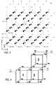
- FIGS. 1 and 2show a three-dimensional color space 100 .
- Various combinations of R, G and B components of the color space 100are represented along separate x, y and z-axes 102 , 104 , 106 , respectively.
- the color space 100 in one applicationis used for transforming an input RGB color value 108 into an output CYM color value.
- the eight lattice points 110 A- 110 Hare identified for a unit cell 220 that contains the input RGB color value 108 .
- the eight lattice points 110 A- 110 Hare interpolated to the input color value 108 to determine the output color values (C, M, Y or K).
- multiple memory spacesmay be used to access the eight lattice point samples 110 A- 110 H.
- One way of assigning lattice points to multiple memory spacesis explained in FIG. 3 .
- lattice pointsare indexed relative to the x, y, z axes 102 , 104 , 106 respectively.
- the lattice point at the origin of color space 100 in FIG. 3is referenced as V( 0 , 0 , 0 ).
- the neighboring lattice point along the x-axisis referenced as V( 1 , 0 , 0 ).
- the next remaining lattice points located sequentially along the x-axisare V( 2 , 0 , 0 ), V( 3 , 0 , 0 ) . . . V( 15 , 0 , 0 ).
- the lattice pointsare referenced as V( 0 , 0 , 0 ), V( 0 , 1 , 0 ), V( 0 , 2 , 0 ) . . . V( 0 , 15 , 0 ).
- Lattice points along the z-axisare referenced as V( 0 , 0 , 0 - 15 ).
- lattice points V( 0 - 3 , 0 , 0 ) along the x-axisare assigned to sequentially referenced memories M 0 , M 1 , M 2 and M 3 , respectively.
- the assignment of lattice points sequentially in memories M 0 -M 3continues along the x-axis 102 .
- lattice points V( 4 - 7 , 0 , 0 )are assigned to memories M 0 -M 3 , respectively.
- lattice points V( 8 - 11 , 0 , 0 )are assigned to memories M 0 -M 3 , respectively, and lattice points V( 12 - 15 , 0 , 0 ) are assigned to memories M 0 -M 3 , respectively.
- the lattice points V( 0 - 15 , 1 , 0 )extend along a next x-axis in a next vertical plane. These lattice points are assigned to memories M 2 , M 3 , M 0 , M 1 , respectively.
- Lattice points V( 0 - 3 , 1 , 0 )are assigned to memories M 2 , M 3 , M 0 , M 1 , respectively; lattice points V( 4 - 7 , 1 , 0 ) are assigned to memories M 2 , M 3 , M 0 , M 1 respectively; lattice points V( 8 - 11 , 1 , 0 ) are assigned to memories M 2 , M 3 , M 0 , M 1 , respectively, and lattice points V( 12 - 15 , 1 , 0 ) are assigned to memories M 2 , M 3 , M 0 , M 1 , respectively.
- the lattice points V( 0 - 15 , 2 , 0 ) along the x-axis of a next vertical planeare assigned to memories in the sequence M 0 -M 3 similar to the x-axis V( 0 - 15 , 0 , 0 ).
- lattice pointsare also assigned sequentially to memories along the x-axis of a next upper horizontal plane. For example, lattice points V( 0 - 3 , 0 , 1 ) are assigned to memories M 4 , M 5 , M 6 , M 7 , respectively. The remaining lattice points along this x-axis are assigned in similar sequential fashion to memories M 4 -M 7 , respectively.
- Lattice points along the y and z axes of the color space 100may be assigned to memories in a mirrored relationship about an intersecting axis.
- lattice point V( 0 , 0 , 1 )may be assigned to memory M 4 .
- the lattice points V( 0 , 0 , 0 ) and V( 0 , 0 , 2 )are each assigned to memory M 0 .
- lattice points immediately above and below lattice point V( 0 , 0 , 2 )are both assigned to the same memory M 4 .
- a similar mirrored relationshipmay exit along the y-axis 104 .
- lattice point ( 0 , 1 , 0 )may be assigned to memory M 2 .
- the lattice points V( 0 , 0 , 0 ) and V( 0 , 2 , 0 ) on opposite sides of V( 0 , 1 , 0 )are both assigned to memory M 0 .
- lattice pointsare assigned to the memories M 0 -M 7 . It should be understood that other lattice point/memory assignment can also be used. For example, more or less than four sequential memories may be used to store sequential lattice points along one of the axes. Also any of these different memory assignments can be used with more than eight memories or less than eight memories.
- the lattice point samplesare assigned to memories M 0 -M 7 in a regular, periodic fashion that use the same lattice point for eight adjacent unit cubes.
- Memory M 7provides the far, upper right-hand lattice point for a unit cube 1 , which is also the far, upper left-hand lattice point for a unit cube 2 .
- Memory M 7also provides the front lower left-hand lattice point for a unit cube 3 .
- address generation logic used for accessing the eight memories M 0 -M 7should generate the same address for the same lattice point contained within eight different unit cubes.
- the address generation logic used for accessing the eight memoriesmust produce eight different addresses (one for each memory) for a given input value in order to access the eight lattice points constituting a unit cube.
- a reorganizationis then needed after accessing memories M 0 -M 7 since any of the eight memories M 0 -M 7 could provide a given lattice point within the unit cube.
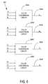
- FIG. 5shows a system for implementing the color transformation scheme described in FIGS. 1-4.
- a set of input RGB color values 502arrives encoded as three 8-bit words. Red may be represented by 8 bit word R[7:0], green by G[7:0], and blue B[7:0].
- R[7:0]8 bit word
- G[7:0]green by G[7:0]
- blue B[7:0]the bit size for the RGB words
- the bit size for the RGB wordscan change for different applications.
- the size of the bit portions 503 and 507 described belowcan also vary depending on the application or the bit size of the RGB words.
- the RGB words 502are divided into an upper 4-bit portion 503 and a lower 4-bit portion 507 . This is convenient because in one example the color transfer function may be sampled at every sixteen units along the RGB axis.
- the upper 4-bits 503 of the RGB input data 502identifies the unit cube 220 (FIG. 2) in which the input RGB data 108 lies.
- the lower 4-bits 507identify where inside the unit cube 220 the input RGB color data 108 is located.
- the number of bits assigned to the high and low divisionscan be different, four high and four low being the preferred embodiment.
- An address generator 504receives the upper 4-bits 503 of the RGB input color data 502 and generates eight separate addresses 506 A- 506 E for memories M 0 -M 7 , respectively.
- the memories M 0 -M 7contain the lattice points for one of the color spaces shown in FIG. 1-4. It should be understood that the memories M 0 -M 7 may comprise any type of memory such as, e.g., dynamic random access memory (DRAM), static random access memory (SRAM), random access memory (RAM), read only memory (ROM) or other volatile or non-volatile memory types.
- DRAMdynamic random access memory
- SRAMstatic random access memory
- RAMrandom access memory
- ROMread only memory
- the eight lattice points 110 A- 110 H for the unit cube 220 surrounding the input color point 108are output to a sample reorder circuit 514 .
- the memories M 0 -M 7may contain a different lattice point for different unit cubes.
- the sample reorder circuit 514uses the upper 4-bits 503 of the input RGB data 502 to reorder the eight lattice points in a known order.
- the interpolator 518then uses the eight reordered lattice points 516 A- 516 H to interpolate to the input color data point 108 identified by the lower 4-bits 507 of the input RGB data 502 .
- the result of the interpolationis the output CYM color data.
- the address generator 504uses the upper four bits R[7:4], G[7:4] and B[7:4] of the input RGB data 502 to generate addresses 506 A- 506 H.
- a set of x, y and z coordinate datamay be related to the input RGB color data 502 through the following equations:
- variable mrepresents a particular one of the memories M 0 -M 7 .
- variable mrepresents one of the integer values 0, 1, 2, 3, 4, 5, 6, or 7.
- a mode valuemay be determined as follows.
- %represents a modulus (remainder) operation. For example, 11%8 is equal to 3 and 16%8 is equal to 0.
- Variables x, y, zmay be redefined by new variables as follows:
- variables C 0 , C 1 , C 2 , C 3 , C 4 and C 5have values for particular memories m as shown in table 1.0.
- different memoriesmay provide different lattice points for different unit cubes 220 .
- memory 510 Amay contain a lattice point for a lower front left corner of the identified unit cube.
- memory 510 Amay contain a lattice point for an upper back left corner of the identified unit cube.
- Sample reorder circuit 514recorders the lattice points output from memories M 0 -M 7 in some common order. For example, sample recorder circuit 514 may reorder the lattice points so that output 516 A outputs the lattice point for the front lower left corner for all unit cubes output from memories M 0 -M 7 .
- the sample recorder circuit 514arranges the lattice points 512 A- 512 H output by the memories M 0 -M 7 according to the upper bits R[7:4], G[7:4] and B[7:4] of the input RGB color data 502 .
- the lattice points 512 A- 512 H in one implementationare reordered to equations 6.0 and 7.0. Of course, other reordering schemes can also be used.
- the lattice points 516 A- 516 Hare referred to as V(n) in equation 6.0 and the memories M 0 -M 7 are referred to as R as follows:
- V ( n )R (( n+o )%8) Equation 6.0
- the x, y, z valuesare derived from equations 2.1-2.3 above.
- the term z[0]refers to the least significant bit of z
- y[1:0]refers to the two least significant bits of y
- x[2:0]refers to the three least significant bits of x.
- a value of 6may be generated for variable o.
- the memory containing the third lattice point for the unit cubecould be derived as follows:
- V (3)R (1) Equation 7.2
- memory M 1outputs the third lattice point for the unit cube output from the memories M 0 -M 7 .
- Interpolator 518interpolates the reordered lattice points 516 A- 516 H to an input RGB color point identified by the lower four RGB bits 507 .
- One example, of an interpolation process that can be used by interpolator 518is described below.
- a cyan value Cmay be obtained using equation 8.0 below by dividing a difference between C values for the lattice points of the unit cube (C 1-C 0 ) by the cubic region width.
- the width of the unit cubeis 16 .
- the width valuecould be some other value.
- the result from the divisionis multiplied by a relative length established by the input color point 108 (FIG. 2) with respect to the surrounding lattice points 110 A- 110 H (FIG. 2 ).
- the result from the multiplicationis added to a base cyan value Co associated with the origin of the unit cube 220 .
- C out( y in - y 0 y 1 - y 0 ) ⁇ ( C 1 - C 0 16 ) + C 0 Equation ⁇ ⁇ 8.0
- magenta (M) and yellow (Y) output valuesare determined by the interpolator 518 in a similar fashion.
- the relative distance term( y in - y 0 y 1 - y 0 )
- R(3:0), G(3:0) and B(3:0) color datamay be derived from the R(3:0), G(3:0) and B(3:0) color data.
- the address generator 504 , sample reorder circuit 514 and interpolator 518can be implemented in software or hardware. For example, these elements may be implemented in software using a programmable processor or may be implemented in hardware using different discrete logic devices.
- the memories M 0 -M 7may be separately addressable memory devices or may be different memory spaces in the same memory device.
- FIG. 6shows separate color conversion circuits 600 A- 600 D used for outputting different CYMK values.
- Color conversion circuit 600 Aoutputs cyan (C) color data 604 A
- circuit 600 Boutputs magenta (M) color data 604 B
- circuit 600 Coutputs yellow (Y) color data 604 C
- circuit 600 Doutputs black (K) color data 604 D.
- Each color conversion circuit 600 A- 600 Dmay contain circuitry similar to that shown in FIG. 5 . However, the contents of the memories M 0 -M 7 in the different color conversion circuits 600 A- 600 D may differ according to the associated output color data 604 A- 604 D, respectively.
- a single itemmay be labeled “first” or “second” or with another such identifier depending on its context or sub-context. This type of identifier may be provided for convenience and shall not necessarily imply that a “second” of something should necessitate a “first”.
- circuits of the exemplary embodimentsmay be disclosed in simplified form (e.g., simplified blocks) in order to avoid obscuring an essence of the exemplary embodiments of the present invention.
- Embodiments of the present inventioninclude devices and methods that may include provisions for conversion of color data.
- the color conversionmay have been described with reference to color data of a first RGB color space and that of a second CMYK color space. It should be understood, however, that the scope of the present invention encompasses any color space that needs transformation into another color space.
- a “print” color spacerepresents a common output domain
- alternative embodimentsmay establish output color data for domains and uses other than printing.
- exemplary embodiments disclosedmay have been described with reference to color spaces of equal dimension.
- exemplary embodimentsmay use R, G, B coordinate axes for a first color space and C, M, Y, K coordinate axes for a second color space.
- the dimensional order of the input and output color spacesdo not have to be the same.
- the second (print) color spacemay comprise four dimensions that include C, M, Y and black (K) coordinate axes.
Landscapes
- Engineering & Computer Science (AREA)
- Multimedia (AREA)
- Signal Processing (AREA)
- Color Image Communication Systems (AREA)
- Facsimile Image Signal Circuits (AREA)
Abstract
Description
| TABLE 1.0 | |||||||
| m | C0 | C1 | C2 | C4 | C5 | ||
| 0 | 77 | 39 | 9 | 2 | 2 | 2 | |
| 1 | 68 | 34 | 8 | 2 | 3 | 3 | |
| 2 | 76 | 38 | 9 | 2 | 3 | 1 | |
| 3 | 68 | 34 | 8 | 2 | 3 | 3 | |
| 4 | 77 | 38 | 9 | 2 | 0 | 2 | |
| 5 | 68 | 34 | 8 | 2 | 3 | 3 | |
| 6 | 76 | 38 | 9 | 2 | 1 | 3 | |
| 7 | 68 | 34 | 8 | 2 | 3 | 3 | |


Claims (19)
Priority Applications (1)
| Application Number | Priority Date | Filing Date | Title |
|---|---|---|---|
| US10/112,383US6753988B1 (en) | 2002-03-29 | 2002-03-29 | Apparatus and method for color data conversion |
Applications Claiming Priority (1)
| Application Number | Priority Date | Filing Date | Title |
|---|---|---|---|
| US10/112,383US6753988B1 (en) | 2002-03-29 | 2002-03-29 | Apparatus and method for color data conversion |
Publications (1)
| Publication Number | Publication Date |
|---|---|
| US6753988B1true US6753988B1 (en) | 2004-06-22 |
Family
ID=32467316
Family Applications (1)
| Application Number | Title | Priority Date | Filing Date |
|---|---|---|---|
| US10/112,383Expired - Fee RelatedUS6753988B1 (en) | 2002-03-29 | 2002-03-29 | Apparatus and method for color data conversion |
Country Status (1)
| Country | Link |
|---|---|
| US (1) | US6753988B1 (en) |
Cited By (5)
| Publication number | Priority date | Publication date | Assignee | Title |
|---|---|---|---|---|
| US20060050288A1 (en)* | 2004-09-09 | 2006-03-09 | International Business Machines Corporation | Method and apparatus for efficient processing of color conversion |
| US20070188814A1 (en)* | 2006-02-15 | 2007-08-16 | Sigma Tel, Inc. | Color conversion system and method |
| US9392143B1 (en)* | 2010-03-31 | 2016-07-12 | Ambarella, Inc. | High performance memory system for 3D color correction |
| CN106488075A (en)* | 2015-08-31 | 2017-03-08 | 京瓷办公信息系统株式会社 | Lattice point group generation method and lattice point group's generating means |
| US11394853B2 (en)* | 2019-09-29 | 2022-07-19 | Boe Technology Group Co., Ltd. | Image representation method, image representation device, and computer readable storage medium |
Citations (12)
| Publication number | Priority date | Publication date | Assignee | Title |
|---|---|---|---|---|
| US3938102A (en) | 1974-08-19 | 1976-02-10 | International Business Machines Corporation | Method and apparatus for accessing horizontal sequences and rectangular sub-arrays from an array stored in a modified word organized random access memory system |
| US3995253A (en) | 1975-03-03 | 1976-11-30 | International Business Machines Corporation | Method and apparatus for accessing horizontal sequences, vertical sequences, and rectangular subarrays from an array stored in a modified word organized random access memory system |
| US4837722A (en) | 1986-05-14 | 1989-06-06 | Massachusetts Institute Of Technology | Digital high speed 3-dimensional interpolation machine |
| JPH0636047A (en)* | 1992-07-16 | 1994-02-10 | Teijin Ltd | Method for generating border surface of body |
| US5666437A (en) | 1996-08-02 | 1997-09-09 | Hewlett-Packard Company | Apparatus for routing interpolator input data by performing a selective two's complement based on sets of lower and higher order bits of input data |
| US5684981A (en) | 1995-01-18 | 1997-11-04 | Hewlett-Packard Company | Memory organization and method for multiple variable digital data transformation |
| US5717507A (en) | 1996-08-02 | 1998-02-10 | Hewlett-Packard Company | Apparatus for generating interpolator input data |
| US5748176A (en)* | 1995-07-20 | 1998-05-05 | Hewlett-Packard Company | Multi-variable colorimetric data access by iterative interpolation and subdivision |
| US5764795A (en)* | 1995-01-26 | 1998-06-09 | Fuji Xerox Co., Ltd. | Color image processing apparatus for color matching and color matching processing method |
| US20010033288A1 (en)* | 2000-03-09 | 2001-10-25 | Takayuki Nabeshima | Color conversion apparatus and method with precision enhancement in color conversion |
| US6415065B1 (en)* | 1995-08-04 | 2002-07-02 | Canon Kabushiki Kaisha | Image processing apparatus and method therefor |
| US20030117415A1 (en)* | 2001-12-11 | 2003-06-26 | Stmicroelectronics, Inc. | Color transformation in 3D color space |
- 2002
- 2002-03-29USUS10/112,383patent/US6753988B1/ennot_activeExpired - Fee Related
Patent Citations (12)
| Publication number | Priority date | Publication date | Assignee | Title |
|---|---|---|---|---|
| US3938102A (en) | 1974-08-19 | 1976-02-10 | International Business Machines Corporation | Method and apparatus for accessing horizontal sequences and rectangular sub-arrays from an array stored in a modified word organized random access memory system |
| US3995253A (en) | 1975-03-03 | 1976-11-30 | International Business Machines Corporation | Method and apparatus for accessing horizontal sequences, vertical sequences, and rectangular subarrays from an array stored in a modified word organized random access memory system |
| US4837722A (en) | 1986-05-14 | 1989-06-06 | Massachusetts Institute Of Technology | Digital high speed 3-dimensional interpolation machine |
| JPH0636047A (en)* | 1992-07-16 | 1994-02-10 | Teijin Ltd | Method for generating border surface of body |
| US5684981A (en) | 1995-01-18 | 1997-11-04 | Hewlett-Packard Company | Memory organization and method for multiple variable digital data transformation |
| US5764795A (en)* | 1995-01-26 | 1998-06-09 | Fuji Xerox Co., Ltd. | Color image processing apparatus for color matching and color matching processing method |
| US5748176A (en)* | 1995-07-20 | 1998-05-05 | Hewlett-Packard Company | Multi-variable colorimetric data access by iterative interpolation and subdivision |
| US6415065B1 (en)* | 1995-08-04 | 2002-07-02 | Canon Kabushiki Kaisha | Image processing apparatus and method therefor |
| US5666437A (en) | 1996-08-02 | 1997-09-09 | Hewlett-Packard Company | Apparatus for routing interpolator input data by performing a selective two's complement based on sets of lower and higher order bits of input data |
| US5717507A (en) | 1996-08-02 | 1998-02-10 | Hewlett-Packard Company | Apparatus for generating interpolator input data |
| US20010033288A1 (en)* | 2000-03-09 | 2001-10-25 | Takayuki Nabeshima | Color conversion apparatus and method with precision enhancement in color conversion |
| US20030117415A1 (en)* | 2001-12-11 | 2003-06-26 | Stmicroelectronics, Inc. | Color transformation in 3D color space |
Cited By (10)
| Publication number | Priority date | Publication date | Assignee | Title |
|---|---|---|---|---|
| US20060050288A1 (en)* | 2004-09-09 | 2006-03-09 | International Business Machines Corporation | Method and apparatus for efficient processing of color conversion |
| US7944593B2 (en) | 2004-09-09 | 2011-05-17 | Infoprint Solutions Company, Llc | Method and apparatus for efficient processing of color conversion |
| US20070188814A1 (en)* | 2006-02-15 | 2007-08-16 | Sigma Tel, Inc. | Color conversion system and method |
| US7586644B2 (en) | 2006-02-15 | 2009-09-08 | Conexant Systems, Inc. | Color conversion system and method |
| US20090323123A1 (en)* | 2006-02-15 | 2009-12-31 | Conexant Systems, Inc. | Color conversion system and method |
| US7933045B2 (en) | 2006-02-15 | 2011-04-26 | Conexant Systems, Inc. | Color conversion system and method |
| US9392143B1 (en)* | 2010-03-31 | 2016-07-12 | Ambarella, Inc. | High performance memory system for 3D color correction |
| CN106488075A (en)* | 2015-08-31 | 2017-03-08 | 京瓷办公信息系统株式会社 | Lattice point group generation method and lattice point group's generating means |
| CN106488075B (en)* | 2015-08-31 | 2019-01-15 | 京瓷办公信息系统株式会社 | Lattice point group generation method and lattice point group's generating means |
| US11394853B2 (en)* | 2019-09-29 | 2022-07-19 | Boe Technology Group Co., Ltd. | Image representation method, image representation device, and computer readable storage medium |
Similar Documents
| Publication | Publication Date | Title |
|---|---|---|
| US5321797A (en) | Apparatus and method for performing coordinate transformation employing stored values and interpolation | |
| KR100364942B1 (en) | Multidimensional data conversion apparatus and method | |
| US5809181A (en) | Color conversion apparatus | |
| EP0822708B1 (en) | Apparatus for generating interpolator input data | |
| US5774386A (en) | Method and apparatus for performing function evaluation using a cache | |
| JP2000505268A (en) | Interpolation method in n-dimensional color space | |
| US6753988B1 (en) | Apparatus and method for color data conversion | |
| US6771275B1 (en) | Processing system and method using a multi-dimensional look-up table | |
| JP2903808B2 (en) | Color signal conversion method and apparatus | |
| US5666437A (en) | Apparatus for routing interpolator input data by performing a selective two's complement based on sets of lower and higher order bits of input data | |
| US7443544B2 (en) | Accelerating color conversion using a temporary palette cache | |
| US5412740A (en) | Signal processing system having reduced memory space | |
| EP1039742A1 (en) | Method of interpolation | |
| US6442297B1 (en) | Storage apparatus and writing and/or reading methods for use in hierarchical coding | |
| US6801212B1 (en) | Apparatus and method for color data interpolation | |
| JP2677954B2 (en) | Memory system | |
| EP0896297A2 (en) | Ram address generation for tetrahedral interpolation | |
| JPH0969961A (en) | Color conversion device | |
| EP0896298A2 (en) | Ram address generation for tetrahaedrische Interpolation über einen hexagonalen Verbund | |
| JP2002354276A (en) | Color conversion method and color conversion device | |
| JP3871027B2 (en) | Color data converter | |
| JP2001008044A (en) | Image processor | |
| US10091397B2 (en) | System including image forming apparatus and lattice point group generating device that generates group of pre-color conversion lattice points to be contained in color conversion table used for conversion of colors in RGB color space to colors in CMYK color space in the image forming apparatus | |
| JP2002044470A (en) | Color conversion processing apparatus and address area allocating method of lookup table in the apparatus | |
| JPH09172554A (en) | Color lookup table |
Legal Events
| Date | Code | Title | Description |
|---|---|---|---|
| AS | Assignment | Owner name:CYPRESS SEMICONDUCTOR CORP., CALIFORNIA Free format text:ASSIGNMENT OF ASSIGNORS INTEREST;ASSIGNOR:ELDREDGE, JAMES G.;REEL/FRAME:012749/0167 Effective date:20020326 | |
| FEPP | Fee payment procedure | Free format text:PAYOR NUMBER ASSIGNED (ORIGINAL EVENT CODE: ASPN); ENTITY STATUS OF PATENT OWNER: LARGE ENTITY | |
| CC | Certificate of correction | ||
| FPAY | Fee payment | Year of fee payment:4 | |
| REMI | Maintenance fee reminder mailed | ||
| FPAY | Fee payment | Year of fee payment:8 | |
| AS | Assignment | Owner name:MORGAN STANLEY SENIOR FUNDING, INC., NEW YORK Free format text:SECURITY INTEREST;ASSIGNORS:CYPRESS SEMICONDUCTOR CORPORATION;SPANSION LLC;REEL/FRAME:035240/0429 Effective date:20150312 | |
| REMI | Maintenance fee reminder mailed | ||
| LAPS | Lapse for failure to pay maintenance fees | ||
| STCH | Information on status: patent discontinuation | Free format text:PATENT EXPIRED DUE TO NONPAYMENT OF MAINTENANCE FEES UNDER 37 CFR 1.362 | |
| FP | Lapsed due to failure to pay maintenance fee | Effective date:20160622 | |
| AS | Assignment | Owner name:SPANSION LLC, CALIFORNIA Free format text:PARTIAL RELEASE OF SECURITY INTEREST IN PATENTS;ASSIGNOR:MORGAN STANLEY SENIOR FUNDING, INC., AS COLLATERAL AGENT;REEL/FRAME:039708/0001 Effective date:20160811 Owner name:CYPRESS SEMICONDUCTOR CORPORATION, CALIFORNIA Free format text:PARTIAL RELEASE OF SECURITY INTEREST IN PATENTS;ASSIGNOR:MORGAN STANLEY SENIOR FUNDING, INC., AS COLLATERAL AGENT;REEL/FRAME:039708/0001 Effective date:20160811 | |
| AS | Assignment | Owner name:MORGAN STANLEY SENIOR FUNDING, INC., NEW YORK Free format text:CORRECTIVE ASSIGNMENT TO CORRECT THE 8647899 PREVIOUSLY RECORDED ON REEL 035240 FRAME 0429. ASSIGNOR(S) HEREBY CONFIRMS THE SECURITY INTERST;ASSIGNORS:CYPRESS SEMICONDUCTOR CORPORATION;SPANSION LLC;REEL/FRAME:058002/0470 Effective date:20150312 |