US6753700B2 - Universal single-ended parallel bus - Google Patents
Universal single-ended parallel busDownload PDFInfo
- Publication number
- US6753700B2 US6753700B2US10/179,735US17973502AUS6753700B2US 6753700 B2US6753700 B2US 6753700B2US 17973502 AUS17973502 AUS 17973502AUS 6753700 B2US6753700 B2US 6753700B2
- Authority
- US
- United States
- Prior art keywords
- differential
- output
- buffer
- data
- differential pair
- Prior art date
- Legal status (The legal status is an assumption and is not a legal conclusion. Google has not performed a legal analysis and makes no representation as to the accuracy of the status listed.)
- Expired - Lifetime
Links
Images


Classifications
- H—ELECTRICITY
- H03—ELECTRONIC CIRCUITRY
- H03K—PULSE TECHNIQUE
- H03K5/00—Manipulating of pulses not covered by one of the other main groups of this subclass
- H03K5/01—Shaping pulses
- H03K5/08—Shaping pulses by limiting; by thresholding; by slicing, i.e. combined limiting and thresholding
- H03K5/082—Shaping pulses by limiting; by thresholding; by slicing, i.e. combined limiting and thresholding with an adaptive threshold
- G—PHYSICS
- G06—COMPUTING OR CALCULATING; COUNTING
- G06F—ELECTRIC DIGITAL DATA PROCESSING
- G06F13/00—Interconnection of, or transfer of information or other signals between, memories, input/output devices or central processing units
- G06F13/38—Information transfer, e.g. on bus
- G06F13/40—Bus structure
- G06F13/4063—Device-to-bus coupling
- G06F13/4068—Electrical coupling
- G06F13/4072—Drivers or receivers
- H—ELECTRICITY
- H03—ELECTRONIC CIRCUITRY
- H03K—PULSE TECHNIQUE
- H03K19/00—Logic circuits, i.e. having at least two inputs acting on one output; Inverting circuits
- H03K19/0175—Coupling arrangements; Interface arrangements
- H03K19/0185—Coupling arrangements; Interface arrangements using field effect transistors only
- H03K19/018507—Interface arrangements
- H03K19/018521—Interface arrangements of complementary type, e.g. CMOS
- H03K19/018528—Interface arrangements of complementary type, e.g. CMOS with at least one differential stage
- H—ELECTRICITY
- H04—ELECTRIC COMMUNICATION TECHNIQUE
- H04L—TRANSMISSION OF DIGITAL INFORMATION, e.g. TELEGRAPHIC COMMUNICATION
- H04L25/00—Baseband systems
- H04L25/02—Details ; arrangements for supplying electrical power along data transmission lines
- H04L25/0264—Arrangements for coupling to transmission lines
- H04L25/0272—Arrangements for coupling to multiple lines, e.g. for differential transmission
- H—ELECTRICITY
- H04—ELECTRIC COMMUNICATION TECHNIQUE
- H04L—TRANSMISSION OF DIGITAL INFORMATION, e.g. TELEGRAPHIC COMMUNICATION
- H04L7/00—Arrangements for synchronising receiver with transmitter
- H04L7/0008—Synchronisation information channels, e.g. clock distribution lines
Definitions
- the present inventionrelates in general to communication systems, and in particular to a communication system using single-ended parallel bus architecture for high speed data communication.
- differential parallel bus architecturesFor high-speed chip to chip communication it is common to find both the clock and parallel data lines using fully differential architecture.
- the differential parallel bus architecturesrequires twice the number of I/O's as compared to the single-ended bus architecture.
- single-ended bus architecturesTo reduce the number of I/Os and bus interconnect lines it is desirable to use single-ended bus architectures.
- the signal swingsare typically small, and in single-ended architectures it becomes necessary to define a reference signal which sets the threshold voltage of the I/O cells. This reference signal is used in both the transmitter as well as the receiver and is used to determine the logic state of the signal.
- a reference signal in a single-ended bus architecturesworks well as long as the reference voltage remains stable and accurate. Any variations in the reference signal results in duty cycle distortions.
- the receiveris typically equipped with circuitry that extracts the reference level from the data. This method of reference extraction, however, still suffers from variations since the DC value of the received data can vary significantly depending on the data stream. There is therefore a need for data communication systems with improved single-ended bus structures.
- the present inventionprovides a single-ended bus architecture for high speed data communication wherein a stable and accurate reference voltage minimizes duty cycle distortion.
- a communication system according to the present inventionincludes a single-ended bus structure that is made up of a differential interconnect line that carries a differential periodic signal such as clock, and one or more single-ended data interconnect lines.
- the reference signal for the single-ended data linesis extracted from the differential clock signal. Given a clock signal with near 50% duty cycle, the stability of the extracted DC value is much improved.
- the present inventionprovides a communication system including a first integrated circuit configured to transmit data and a periodic signal; a bus coupled to the first integrated circuit, the bus having at least one differential interconnect line coupled to carry the periodic signal, and a single-ended interconnect line coupled to carry data; and a second integrated circuit configured to receive the data and the periodic signal, the second integrated circuit having a differential buffer coupled to receive the periodic signal and to extract a reference signal, and a data buffer coupled to receive the data and the reference signal.
- the present inventionprovides a method of communicating data including transmitting a differential periodic signal over differential lines in a communication bus; transmitting single-ended data over single-ended lines in the communication bus; and extracting a reference signal for the single-ended data from the differential periodic signal.
- the present inventionprovides an integrated circuit including a differential buffer coupled to receive a differential periodic signal and to extract a DC reference signal from the differential periodic signal; a data buffer coupled to receive a single-ended data and the reference signal, the data buffer being configured to determine a logic level of the single-ended data by comparing it to the reference signal.
- FIG. 1is a high level block diagram of a communication system using the single-ended bus architecture according to the present invention
- FIG. 2shows a simplified circuit schematic for a reference signal extraction circuit according to an exemplary embodiment of the present invention.
- FIG. 3is an exemplary circuit schematic for a data input buffer receiving single-ended data and the extracted reference signal.
- the present inventionprovides a single-ended bus architecture for high speed data communication wherein a stable and accurate reference voltage minimizes duty cycle distortion.
- the source of the datais the same circuit that supplies the clock signal.
- data and clocktypically have the same logic levels (e.g., TTL, CMOS, etc.).
- clockis typically a signal with a 50% duty cycle and therefore has a much more stable DC value.
- the optimum reference voltageis extracted from the clock. This results in a much more accurate and stable reference voltage for use along with single-ended data lines.
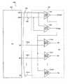
- FIG. 1is a high level block diagram of a communication system 1100 using the single-ended bus architecture according to the present invention.
- a transmitter integrated circuit (IC) 102is connected to a receiver IC 104 via a communication bus 106 .
- Integrated circuits 102 and 194are identified herein as transmitter and receiver for simplicity, and may comprise other circuitry, for example, each being both a transmitter and a receiver (i.e., transceivers).
- bus 106has at least one differential line 108 which is used for carrying clock signal (CKN/CKP) with several other single-ended lines 110 - 0 to 110 - n that carry data.
- CKN/CKPclock signal
- Receiver IC 104includes a differential buffer 112 that receives differential clock signal CKN/CKP and generates the reference signal V REF by extracting the DC value of the differential clock signal. Receiver IC 104 further includes data input buffers 114 - 0 to 114 - n that receive data lines 110 - 0 to 110 - n at their inputs, respectively. Each data input buffer 114 - i is also supplied with the reference signal V REF generated by differential buffer 112 . In one embodiment, the reference signal V REF is also supplied to a clock buffer 116 that is used to buffer the received differential clock signal CKN/CKP and to generate an internal clock signal CK_INT. Single-ended data is thus received and buffered using the reference signal extracted from the differential clock signal.
- Buffer 112for extracting the reference signal V REF from the differential clock signal CKN/CKP.
- Buffer 112includes an input differential pair 200 made-up of n-channel input MOS transistors M 1 and M 2 that receive the differential clock signal CKN/CKP at their respective gate terminals, p-channel load MOS transistors M 3 and M 4 , and n-channel current-source MOS transistor MS.
- Differential clock signal CKN/CKPis buffered and amplified by input differential pair 200 at the output OUT 1 .
- Output OUT 1 of input differential pair 200is filtered by resistor R and capacitor C 1 extracting the DC value of the differential clock signal.
- Resistor Rmay be made of any number of semiconductor materials such as polysilicon, and capacitor C 1 may be made of any number of materials including, for example, an MOS structure as shown.
- a second differential pair 204constructed similar to differential pair 200 , provides buffering and generates V REF at its output.
- FIG. 3shows an exemplary circuit implementation for a data buffer according to the present invention.
- Data buffer 114includes an input differential pair 300 that is capable of receiving either a differential data signal (Din or Dout) or a single-ended signal (e.g., at input Dip).
- Resistors R 1 , R 2 and R 3 , R 4respectively couple to the positive input Dip and negative input Din: These resistors provide for DC biasing of the input terminals.
- the data signal at the output node N 1is applied to one input of comparator 302 that receives at another input the reference signal V REF extracted from the differential clock. By comparing the level of the data signal to V REF , buffer 302 determines the logic level of the data signal.
- One or more invertersdrive the output of the comparators 302 . It is to be understood that give the single-ended data line, data buffer 114 need not provide the capability to receive a differential signal. That is, input differential pair 300 may be a simple inverter receiving a single-ended signal.
- the present inventionthus provides a single-ended bus structure for high speed data communication systems wherein the reference signal is extracted from a differential periodic signal.
- the reference signal as thus extractedis much more stable and accurate minimizing distortion in the duty cycle of the data signal.
- the differential signalhas been identified as clock
- the advantages of the present inventioncan be obtained with any periodic signal, whether defined as clock or another signal.
- the number of differential and single-ended interconnect lines in the bus according to the present inventionmay vary depending on the system requirements. Therefore, the scope of the present invention should be determined not with reference to the above description but should, instead, be determined with reference to the appended claims, along with their full scope of equivalents.
Landscapes
- Engineering & Computer Science (AREA)
- Physics & Mathematics (AREA)
- General Engineering & Computer Science (AREA)
- Computer Hardware Design (AREA)
- Signal Processing (AREA)
- Computer Networks & Wireless Communication (AREA)
- Theoretical Computer Science (AREA)
- Nonlinear Science (AREA)
- Computing Systems (AREA)
- Power Engineering (AREA)
- Mathematical Physics (AREA)
- General Physics & Mathematics (AREA)
- Dc Digital Transmission (AREA)
Abstract
Description
Claims (20)
Priority Applications (3)
| Application Number | Priority Date | Filing Date | Title |
|---|---|---|---|
| US10/179,735US6753700B2 (en) | 1999-06-28 | 2002-06-24 | Universal single-ended parallel bus |
| US10/856,476US7135889B2 (en) | 1999-06-28 | 2004-05-29 | Universal single-ended parallel bus |
| US11/591,406US7312639B2 (en) | 1999-06-28 | 2006-11-01 | Universal single-ended parallel bus |
Applications Claiming Priority (3)
| Application Number | Priority Date | Filing Date | Title |
|---|---|---|---|
| US14135499P | 1999-06-28 | 1999-06-28 | |
| US09/605,091US6424177B1 (en) | 1999-06-28 | 2000-06-27 | Universal single-ended parallel bus |
| US10/179,735US6753700B2 (en) | 1999-06-28 | 2002-06-24 | Universal single-ended parallel bus |
Related Parent Applications (1)
| Application Number | Title | Priority Date | Filing Date |
|---|---|---|---|
| US09/605,091ContinuationUS6424177B1 (en) | 1999-06-28 | 2000-06-27 | Universal single-ended parallel bus |
Related Child Applications (1)
| Application Number | Title | Priority Date | Filing Date |
|---|---|---|---|
| US10/856,476ContinuationUS7135889B2 (en) | 1999-06-28 | 2004-05-29 | Universal single-ended parallel bus |
Publications (2)
| Publication Number | Publication Date |
|---|---|
| US20020175709A1 US20020175709A1 (en) | 2002-11-28 |
| US6753700B2true US6753700B2 (en) | 2004-06-22 |
Family
ID=26839024
Family Applications (4)
| Application Number | Title | Priority Date | Filing Date |
|---|---|---|---|
| US09/605,091Expired - LifetimeUS6424177B1 (en) | 1999-06-28 | 2000-06-27 | Universal single-ended parallel bus |
| US10/179,735Expired - LifetimeUS6753700B2 (en) | 1999-06-28 | 2002-06-24 | Universal single-ended parallel bus |
| US10/856,476Expired - LifetimeUS7135889B2 (en) | 1999-06-28 | 2004-05-29 | Universal single-ended parallel bus |
| US11/591,406Expired - LifetimeUS7312639B2 (en) | 1999-06-28 | 2006-11-01 | Universal single-ended parallel bus |
Family Applications Before (1)
| Application Number | Title | Priority Date | Filing Date |
|---|---|---|---|
| US09/605,091Expired - LifetimeUS6424177B1 (en) | 1999-06-28 | 2000-06-27 | Universal single-ended parallel bus |
Family Applications After (2)
| Application Number | Title | Priority Date | Filing Date |
|---|---|---|---|
| US10/856,476Expired - LifetimeUS7135889B2 (en) | 1999-06-28 | 2004-05-29 | Universal single-ended parallel bus |
| US11/591,406Expired - LifetimeUS7312639B2 (en) | 1999-06-28 | 2006-11-01 | Universal single-ended parallel bus |
Country Status (1)
| Country | Link |
|---|---|
| US (4) | US6424177B1 (en) |
Cited By (2)
| Publication number | Priority date | Publication date | Assignee | Title |
|---|---|---|---|---|
| US20030087671A1 (en)* | 2001-11-02 | 2003-05-08 | Nokia Corporation | Multi-mode I/O circuitry supporting low interference signaling schemes for high speed digital interfaces |
| US20040217777A1 (en)* | 1999-06-28 | 2004-11-04 | Armond Hairapetian | Universal single-ended parallel bus |
Families Citing this family (17)
| Publication number | Priority date | Publication date | Assignee | Title |
|---|---|---|---|---|
| US6801584B1 (en)* | 2000-07-05 | 2004-10-05 | Sun Microsystems, Inc. | Using a differential signal in adjusting a slice voltage for a single-ended signal |
| DE102004055859B3 (en)* | 2004-11-19 | 2006-06-08 | Infineon Technologies Ag | Method for transmitting and receiving a data signal on a line pair and transmitting and receiving circuit therefor |
| BRPI0605714B1 (en)* | 2006-03-07 | 2018-06-26 | José Gouveia Abrunhosa Jorge | DEVICE AND PROCESS FOR DETECTION OF MAGNETIC MATERIALS IN ELECTROMAGNETIC TECHNOLOGY ANTI-THEFT SYSTEMS |
| KR100744141B1 (en) | 2006-07-21 | 2007-08-01 | 삼성전자주식회사 | Virtual differential interconnect circuit and virtual differential signaling scheme for single-ended signal lines |
| US7823003B1 (en)* | 2007-01-23 | 2010-10-26 | 3Par, Inc. | Voltage referencing clock for source-synchronous multi-level signal buses |
| US7805545B2 (en)* | 2007-02-07 | 2010-09-28 | Honeywell International Inc. | Method for implementing a control channel in a system of circumvention and recovery |
| US7694187B2 (en)* | 2007-02-07 | 2010-04-06 | Honeywell International Inc. | Method of peripheral type identification in a system of circumvention and recovery |
| US7657785B2 (en)* | 2007-02-07 | 2010-02-02 | Honeywell International Inc. | System of circumvention and recovery in a multi-function system |
| US7761721B2 (en)* | 2007-04-12 | 2010-07-20 | Honeywell International Inc. | System of integrated environmentally hardened architecture for space application |
| US7605635B2 (en)* | 2007-05-24 | 2009-10-20 | National Semiconductor Corporation | Threshold control circuitry for multiple current signal receivers |
| US9838536B2 (en) | 2013-09-30 | 2017-12-05 | Elwha, Llc | Mobile device sharing facilitation methods and systems |
| US9805208B2 (en) | 2013-09-30 | 2017-10-31 | Elwha Llc | Mobile device sharing facilitation methods and systems with recipient-dependent inclusion of a data selection |
| US9774728B2 (en) | 2013-09-30 | 2017-09-26 | Elwha Llc | Mobile device sharing facilitation methods and systems in a context of plural communication records |
| US9740875B2 (en) | 2013-09-30 | 2017-08-22 | Elwha Llc | Mobile device sharing facilitation methods and systems featuring exclusive data presentation |
| US9813891B2 (en) | 2013-09-30 | 2017-11-07 | Elwha Llc | Mobile device sharing facilitation methods and systems featuring a subset-specific source identification |
| US9826439B2 (en) | 2013-09-30 | 2017-11-21 | Elwha Llc | Mobile device sharing facilitation methods and systems operable in network equipment |
| US12362841B2 (en)* | 2023-06-30 | 2025-07-15 | Qualcomm Incorporated | Data communication apparatus with receiver employing transmitter supply voltage noise compensation |
Citations (7)
| Publication number | Priority date | Publication date | Assignee | Title |
|---|---|---|---|---|
| US5710516A (en) | 1995-04-24 | 1998-01-20 | Samsung Electronics Co., Ltd. | Input logic signal buffer circuits |
| US5847581A (en) | 1996-12-31 | 1998-12-08 | Intel Corporation | Low power CMOS precision input receiver with integrated reference |
| US5850163A (en) | 1997-03-31 | 1998-12-15 | Sun Microsystems, Inc. | Active inductor oscillator with wide frequency range |
| US5900745A (en) | 1995-07-28 | 1999-05-04 | Nec Corporation | Semiconductor device including input buffer circuit capable of amplifying input signal with low amplitude in high speed and under low current consumption |
| US6064233A (en) | 1994-08-30 | 2000-05-16 | Oki Electric Industry Co., Ltd. | Semiconductor integrated circuit measuring current to test damaged transistor |
| US6154498A (en) | 1997-09-26 | 2000-11-28 | Intel Corporation | Computer system with a semi-differential bus signaling scheme |
| US6154047A (en) | 1996-07-03 | 2000-11-28 | Fujitsu Limited | Bus configuration and input/output buffer |
Family Cites Families (102)
| Publication number | Priority date | Publication date | Assignee | Title |
|---|---|---|---|---|
| CA1153076A (en) | 1979-12-10 | 1983-08-30 | General Electric Company | Resonator coupled differential amplifier |
| FR2494465B1 (en) | 1980-11-14 | 1987-02-13 | Epd Engineering Projectdevelop | POCKET COMPUTER |
| US4449248A (en) | 1982-02-01 | 1984-05-15 | General Electric Company | Battery saving radio circuit and system |
| JPS5968072A (en) | 1982-10-13 | 1984-04-17 | Sharp Corp | Small electronic device for function conversion |
| US4519068A (en) | 1983-07-11 | 1985-05-21 | Motorola, Inc. | Method and apparatus for communicating variable length messages between a primary station and remote stations of a data communications system |
| US4737975A (en) | 1984-09-18 | 1988-04-12 | Metrofone, Inc. | Programmable system for interfacing a standard telephone set with a radio transceiver |
| US4731796A (en) | 1984-10-25 | 1988-03-15 | Stc, Plc | Multi-mode radio transceiver |
| US4680787A (en) | 1984-11-21 | 1987-07-14 | Motorola, Inc. | Portable radiotelephone vehicular converter and remote handset |
| GB8521159D0 (en) | 1985-08-23 | 1985-10-02 | Pa Consulting Services | Two-way radio communications system |
| US4807282A (en) | 1985-12-30 | 1989-02-21 | International Business Machines Corp. | Programmable P/C compatible communications card |
| JPH06105884B2 (en) | 1986-05-06 | 1994-12-21 | 日本電気株式会社 | Wireless telephone system |
| US4850009A (en) | 1986-05-12 | 1989-07-18 | Clinicom Incorporated | Portable handheld terminal including optical bar code reader and electromagnetic transceiver means for interactive wireless communication with a base communications station |
| US5239662A (en) | 1986-09-15 | 1993-08-24 | Norand Corporation | System including multiple device communications controller which coverts data received from two different customer transaction devices each using different communications protocols into a single communications protocol |
| KR910008738B1 (en) | 1987-02-20 | 1991-10-19 | 닛본 덴기 가부시기가이샤 | Portable radio apparatus having battery saved channel scanning function |
| US4817115A (en) | 1987-02-27 | 1989-03-28 | Telxon Corporation | Encoding and decoding system for electronic data communication system |
| US4777657A (en) | 1987-04-01 | 1988-10-11 | Iss Engineering, Inc. | Computer controlled broadband receiver |
| US4804954A (en) | 1987-04-30 | 1989-02-14 | Motorola, Inc. | Battery saving method for portable communications receivers |
| US5249302A (en) | 1987-10-09 | 1993-09-28 | Motorola, Inc. | Mixed-mode transceiver system |
| US5055660A (en) | 1988-06-16 | 1991-10-08 | Avicom International, Inc. | Portable transaction monitoring unit for transaction monitoring and security control systems |
| JP2583578B2 (en) | 1988-07-01 | 1997-02-19 | 三菱電機株式会社 | Pocket phone |
| US5117501A (en) | 1988-08-08 | 1992-05-26 | General Electric Company | Dynamic regrouping in a trunked radio communications system |
| US5087099A (en) | 1988-09-02 | 1992-02-11 | Stolar, Inc. | Long range multiple point wireless control and monitoring system |
| US4916441A (en) | 1988-09-19 | 1990-04-10 | Clinicom Incorporated | Portable handheld terminal |
| JP2805767B2 (en) | 1988-09-26 | 1998-09-30 | 日本電気株式会社 | Wireless transceiver |
| US4894792A (en) | 1988-09-30 | 1990-01-16 | Tandy Corporation | Portable computer with removable and replaceable add-on modules |
| US5008879B1 (en) | 1988-11-14 | 2000-05-30 | Datapoint Corp | Lan with interoperative multiple operational capabilities |
| US4995099A (en) | 1988-12-01 | 1991-02-19 | Motorola, Inc. | Power conservation method and apparatus for a portion of a predetermined signal |
| US5025486A (en) | 1988-12-09 | 1991-06-18 | Dallas Semiconductor Corporation | Wireless communication system with parallel polling |
| GB2226475A (en) | 1988-12-23 | 1990-06-27 | Philips Electronic Associated | Power economising in multiple user radio systems |
| US5150361A (en) | 1989-01-23 | 1992-09-22 | Motorola, Inc. | Energy saving protocol for a TDM radio |
| US5128938A (en) | 1989-03-03 | 1992-07-07 | Motorola, Inc. | Energy saving protocol for a communication system |
| US5839051A (en) | 1989-03-17 | 1998-11-17 | Technophone Limited | Host radio telephone to directly access a handset NAM through a connecter without requiring the handset controller to be employed |
| US6014705A (en) | 1991-10-01 | 2000-01-11 | Intermec Ip Corp. | Modular portable data processing terminal having a higher layer and lower layer partitioned communication protocol stack for use in a radio frequency communications network |
| US5428636A (en) | 1993-05-03 | 1995-06-27 | Norand Corporation | Radio frequency local area network |
| US5680633A (en) | 1990-01-18 | 1997-10-21 | Norand Corporation | Modular, portable data processing terminal for use in a radio frequency communication network |
| US5029183A (en) | 1989-06-29 | 1991-07-02 | Symbol Technologies, Inc. | Packet data communication network |
| US4969206A (en) | 1989-07-18 | 1990-11-06 | Phyle Industries Limited | Portable data collection device with RF transmission |
| US4964121A (en) | 1989-08-30 | 1990-10-16 | Motorola, Inc. | Battery saver for a TDM system |
| US5121408A (en) | 1989-10-16 | 1992-06-09 | Hughes Aircraft Company | Synchronization for entry to a network in a frequency hopping communication system |
| AU6721890A (en) | 1989-11-03 | 1991-05-31 | Microcom Systems, Inc. | Method and apparatus for effecting efficient transmission of data |
| AU7788191A (en) | 1989-11-22 | 1991-06-13 | David C. Russell | Computer control system |
| US5153878A (en) | 1989-12-11 | 1992-10-06 | Motorola Inc. | Radio data communications system with diverse signaling capability |
| US5055659A (en) | 1990-02-06 | 1991-10-08 | Amtech Technology Corp. | High speed system for reading and writing data from and into remote tags |
| JPH0810995Y2 (en) | 1990-02-08 | 1996-03-29 | 沖電気工業株式会社 | Car phone adapter |
| EP0518926B1 (en) | 1990-03-03 | 1995-08-16 | Cedardell Limited | Communications system |
| GB2241851A (en) | 1990-03-09 | 1991-09-11 | Philips Electronic Associated | Optimising transmitter power in a communications system |
| US5179666A (en) | 1990-06-07 | 1993-01-12 | Unisys Corporation | Block oriented peripheral device interface |
| US5363121A (en) | 1990-06-29 | 1994-11-08 | International Business Machines Corporation | Multiple protocol communication interface for distributed transaction processing |
| US5584048A (en) | 1990-08-17 | 1996-12-10 | Motorola, Inc. | Beacon based packet radio standby energy saver |
| US5119502A (en) | 1990-08-30 | 1992-06-02 | Telefonaktiebolaget L M Ericsson | Periodic system ordered rescan in a cellular communication system |
| JP2646831B2 (en) | 1990-10-25 | 1997-08-27 | 日本電気株式会社 | Selective call receiver |
| US5181200A (en) | 1990-10-29 | 1993-01-19 | International Business Machines Corporation | Handoff method and apparatus for mobile wireless workstation |
| US5265270A (en) | 1990-10-31 | 1993-11-23 | Motorola, Inc. | Method and apparatus for providing power conservation in a communication system |
| US5179721A (en) | 1990-11-05 | 1993-01-12 | Motorola Inc. | Method for inter operation of a cellular communication system and a trunking communication system |
| CA2096832C (en) | 1990-11-26 | 1996-08-20 | Daniel R. Tayloe | Method and apparatus for paging in a communication system |
| US5230084A (en) | 1990-12-06 | 1993-07-20 | Motorola, Inc. | Selective call receiver having extended battery saving capability |
| JP2530060B2 (en) | 1991-01-17 | 1996-09-04 | 株式会社東芝 | Communication control device |
| US5297144A (en) | 1991-01-22 | 1994-03-22 | Spectrix Corporation | Reservation-based polling protocol for a wireless data communications network |
| US5265238A (en) | 1991-01-25 | 1993-11-23 | International Business Machines Corporation | Automatic device configuration for dockable portable computers |
| US5081402A (en) | 1991-02-22 | 1992-01-14 | Comfortex Corporation | Low power consumption wireless data transmission and control system |
| US5134347A (en) | 1991-02-22 | 1992-07-28 | Comfortex Corporation | Low power consumption wireless data transmission and control system |
| US5152006A (en) | 1991-02-25 | 1992-09-29 | Motorola, Inc. | Receiver controller method and apparatus |
| DE69126604T2 (en) | 1991-03-13 | 1998-01-08 | Ibm | Adaptation device and method for the effective connection of data processing devices and networks |
| CA2040234C (en) | 1991-04-11 | 2000-01-04 | Steven Messenger | Wireless coupling of devices to wired network |
| US5249220A (en) | 1991-04-18 | 1993-09-28 | Rts Electronics, Inc. | Handheld facsimile and alphanumeric message transceiver operating over telephone or wireless networks |
| JP2930257B2 (en) | 1991-04-22 | 1999-08-03 | 株式会社東芝 | Portable electronic devices |
| US6374311B1 (en) | 1991-10-01 | 2002-04-16 | Intermec Ip Corp. | Communication network having a plurality of bridging nodes which transmit a beacon to terminal nodes in power saving state that it has messages awaiting delivery |
| DE69232943T2 (en) | 1991-05-13 | 2003-08-28 | Xircom Wireless, Inc. | TRANSMITTER / RECEIVER WITH TWO OPERATING MODES |
| US5394436A (en) | 1991-10-01 | 1995-02-28 | Norand Corporation | Radio frequency local area network |
| US5940771A (en) | 1991-05-13 | 1999-08-17 | Norand Corporation | Network supporting roaming, sleeping terminals |
| US5123029A (en) | 1991-06-21 | 1992-06-16 | International Business Machines Corporation | Broadcast-initiated bipartite frame multi-access protocol |
| GB9114808D0 (en) | 1991-07-09 | 1991-08-28 | Philips Electronic Associated | Information transmission system |
| US5293639A (en) | 1991-08-09 | 1994-03-08 | Motorola, Inc. | Reduction of power consumption in a portable communication unit |
| US5241542A (en) | 1991-08-23 | 1993-08-31 | International Business Machines Corporation | Battery efficient operation of scheduled access protocol |
| US5361397A (en) | 1991-08-26 | 1994-11-01 | Motorola, Inc. | Communication device and system capable of automatic programmable energizing |
| US5392023A (en) | 1991-09-06 | 1995-02-21 | Motorola, Inc. | Data communication system with automatic power control |
| US5390206A (en) | 1991-10-01 | 1995-02-14 | American Standard Inc. | Wireless communication system for air distribution system |
| US5274666A (en) | 1991-10-16 | 1993-12-28 | Telephonics Corporation | Wireless communication system |
| JP2571655B2 (en) | 1991-11-27 | 1997-01-16 | インターナショナル・ビジネス・マシーンズ・コーポレイション | Protocol conversion mechanism, switching network and computer system |
| US5440560A (en) | 1991-12-24 | 1995-08-08 | Rypinski; Chandos A. | Sleep mode and contention resolution within a common channel medium access method |
| ATE207679T1 (en) | 1992-04-20 | 2001-11-15 | 3Com Corp | DEVICE FOR EXPANSION OF NETWORK MEANS TO REMOTE NETWORKS |
| US5744366A (en) | 1992-05-01 | 1998-04-28 | Trustees Of The University Of Pennsylvania | Mesoscale devices and methods for analysis of motile cells |
| EP0648404B1 (en) | 1992-06-29 | 1998-11-25 | Elonex Technologies, Inc. | Modular notebook computer |
| US5579487A (en) | 1992-10-02 | 1996-11-26 | Teletransaction, Inc. | Portable work slate computer with multiple docking positions for interchangeably receiving removable modules |
| US5426637A (en) | 1992-12-14 | 1995-06-20 | International Business Machines Corporation | Methods and apparatus for interconnecting local area networks with wide area backbone networks |
| US5373149A (en) | 1993-02-01 | 1994-12-13 | At&T Bell Laboratories | Folding electronic card assembly |
| US5406643A (en) | 1993-02-11 | 1995-04-11 | Motorola, Inc. | Method and apparatus for selecting between a plurality of communication paths |
| EP0639314B1 (en) | 1993-03-04 | 2003-05-28 | Telefonaktiebolaget Lm Ericsson | Modular radio communications system |
| US5630061A (en) | 1993-04-19 | 1997-05-13 | International Business Machines Corporation | System for enabling first computer to communicate over switched network with second computer located within LAN by using media access control driver in different modes |
| US5796727A (en) | 1993-04-30 | 1998-08-18 | International Business Machines Corporation | Wide-area wireless lan access |
| US5438329A (en) | 1993-06-04 | 1995-08-01 | M & Fc Holding Company, Inc. | Duplex bi-directional multi-mode remote instrument reading and telemetry system |
| US5444763A (en) | 1993-06-17 | 1995-08-22 | Research In Motion Limited | Translation and connection device for radio frequency point of sale transaction systems |
| US5418837A (en) | 1993-07-30 | 1995-05-23 | Ericsson-Ge Mobile Communications Inc. | Method and apparatus for upgrading cellular mobile telephones |
| US5406615A (en) | 1993-08-04 | 1995-04-11 | At&T Corp. | Multi-band wireless radiotelephone operative in a plurality of air interface of differing wireless communications systems |
| US5544222A (en) | 1993-11-12 | 1996-08-06 | Pacific Communication Sciences, Inc. | Cellular digtial packet data mobile data base station |
| JPH07264042A (en)* | 1994-03-17 | 1995-10-13 | Fujitsu Ltd | High speed interface circuit |
| US5488306A (en)* | 1994-05-31 | 1996-01-30 | International Business Machines Corp. | Open and short fault detector for a differential interface |
| US6184717B1 (en)* | 1998-12-09 | 2001-02-06 | Nortel Networks Limited | Digital signal transmitter and receiver using source based reference logic levels |
| US6278312B1 (en)* | 1999-02-24 | 2001-08-21 | Intel Corporation | Method and apparatus for generating a reference voltage signal derived from complementary signals |
| US6424194B1 (en) | 1999-06-28 | 2002-07-23 | Broadcom Corporation | Current-controlled CMOS logic family |
| US6424177B1 (en)* | 1999-06-28 | 2002-07-23 | Broadcom Corporation | Universal single-ended parallel bus |
| US6124177A (en)* | 1999-08-13 | 2000-09-26 | Taiwan Semiconductor Manufacturing Company | Method for making deep sub-micron mosfet structures having improved electrical characteristics |
- 2000
- 2000-06-27USUS09/605,091patent/US6424177B1/ennot_activeExpired - Lifetime
- 2002
- 2002-06-24USUS10/179,735patent/US6753700B2/ennot_activeExpired - Lifetime
- 2004
- 2004-05-29USUS10/856,476patent/US7135889B2/ennot_activeExpired - Lifetime
- 2006
- 2006-11-01USUS11/591,406patent/US7312639B2/ennot_activeExpired - Lifetime
Patent Citations (7)
| Publication number | Priority date | Publication date | Assignee | Title |
|---|---|---|---|---|
| US6064233A (en) | 1994-08-30 | 2000-05-16 | Oki Electric Industry Co., Ltd. | Semiconductor integrated circuit measuring current to test damaged transistor |
| US5710516A (en) | 1995-04-24 | 1998-01-20 | Samsung Electronics Co., Ltd. | Input logic signal buffer circuits |
| US5900745A (en) | 1995-07-28 | 1999-05-04 | Nec Corporation | Semiconductor device including input buffer circuit capable of amplifying input signal with low amplitude in high speed and under low current consumption |
| US6154047A (en) | 1996-07-03 | 2000-11-28 | Fujitsu Limited | Bus configuration and input/output buffer |
| US5847581A (en) | 1996-12-31 | 1998-12-08 | Intel Corporation | Low power CMOS precision input receiver with integrated reference |
| US5850163A (en) | 1997-03-31 | 1998-12-15 | Sun Microsystems, Inc. | Active inductor oscillator with wide frequency range |
| US6154498A (en) | 1997-09-26 | 2000-11-28 | Intel Corporation | Computer system with a semi-differential bus signaling scheme |
Cited By (6)
| Publication number | Priority date | Publication date | Assignee | Title |
|---|---|---|---|---|
| US20040217777A1 (en)* | 1999-06-28 | 2004-11-04 | Armond Hairapetian | Universal single-ended parallel bus |
| US7135889B2 (en)* | 1999-06-28 | 2006-11-14 | Broadcom Corporation | Universal single-ended parallel bus |
| US20030087671A1 (en)* | 2001-11-02 | 2003-05-08 | Nokia Corporation | Multi-mode I/O circuitry supporting low interference signaling schemes for high speed digital interfaces |
| US20090190639A1 (en)* | 2001-11-02 | 2009-07-30 | Nokia Corporation | Multi-mode I/O circuitry supporting low interference signaling schemes for high speed digital interfaces |
| US7702293B2 (en)* | 2001-11-02 | 2010-04-20 | Nokia Corporation | Multi-mode I/O circuitry supporting low interference signaling schemes for high speed digital interfaces |
| US8965304B2 (en) | 2001-11-02 | 2015-02-24 | Nokia Corporation | Multi-mode I/O circuitry supporting low interference signaling schemes for high speed digital interfaces |
Also Published As
| Publication number | Publication date |
|---|---|
| US20040217777A1 (en) | 2004-11-04 |
| US20020175709A1 (en) | 2002-11-28 |
| US6424177B1 (en) | 2002-07-23 |
| US7312639B2 (en) | 2007-12-25 |
| US20070046334A1 (en) | 2007-03-01 |
| US7135889B2 (en) | 2006-11-14 |
Similar Documents
| Publication | Publication Date | Title |
|---|---|---|
| US7312639B2 (en) | Universal single-ended parallel bus | |
| US5606268A (en) | Differential to single-ended CMOS converter | |
| EP0475711B1 (en) | System for transferring data between IC chips | |
| US6046638A (en) | Receive amplifier for reception of high-speed data signals | |
| US20060256744A1 (en) | Bi-directional bridge circuit having high common mode rejection and high input sensitivity | |
| US7847583B2 (en) | Transmitter and receiver using asymmetric transfer characteristics in differential amplifiers to suppress noise | |
| US6320422B1 (en) | Complementary source coupled logic | |
| US8000672B2 (en) | Rail-to-rail data receiver for high-speed communication | |
| EP0746929B1 (en) | High speed differential receiver for data communications | |
| ITVA20010048A1 (en) | ANALOGUE INPUT CIRCUIT WITH COMMON MODE COMPATIBILITY TOWARDS BOTH POWER SUPPLIES | |
| EP4338158B1 (en) | Dynamic cross-coupled regeneration for high-speed sense amplifier | |
| CN114221641B (en) | Rapid comparator circuit for wide common-mode input voltage | |
| US7058121B1 (en) | Logic gates including diode-connected metal-oxide-semiconductor field-effect transistors (MOSFETS) to control input threshold voltage levels and switching transients of output logic signals | |
| KR100661310B1 (en) | High speed interface circuit | |
| US7482838B2 (en) | High-speed differential receiver | |
| US4663546A (en) | Two state synchronizer | |
| CN116150072B (en) | Clock signal receiving circuit, clock signal receiving device and electronic equipment | |
| US12028057B2 (en) | Receivers for high density and low latency chip-to-chip links | |
| US7345605B2 (en) | Pulse amplitude-modulated signal processing | |
| US5942995A (en) | Return-to-zero receiver | |
| GB2432468A (en) | An integrated optical SERDES transceiver circuit using LVDS amplifiers | |
| KR100723468B1 (en) | Signal level converter | |
| CN117353717A (en) | Comparator circuit and signal control method | |
| JPH07154431A (en) | Signal transmission method and CMOS logic integrated circuit |
Legal Events
| Date | Code | Title | Description |
|---|---|---|---|
| FEPP | Fee payment procedure | Free format text:PAYOR NUMBER ASSIGNED (ORIGINAL EVENT CODE: ASPN); ENTITY STATUS OF PATENT OWNER: LARGE ENTITY | |
| STCF | Information on status: patent grant | Free format text:PATENTED CASE | |
| FEPP | Fee payment procedure | Free format text:PAYER NUMBER DE-ASSIGNED (ORIGINAL EVENT CODE: RMPN); ENTITY STATUS OF PATENT OWNER: LARGE ENTITY Free format text:PAYOR NUMBER ASSIGNED (ORIGINAL EVENT CODE: ASPN); ENTITY STATUS OF PATENT OWNER: LARGE ENTITY | |
| FPAY | Fee payment | Year of fee payment:4 | |
| FPAY | Fee payment | Year of fee payment:8 | |
| FPAY | Fee payment | Year of fee payment:12 | |
| AS | Assignment | Owner name:BANK OF AMERICA, N.A., AS COLLATERAL AGENT, NORTH CAROLINA Free format text:PATENT SECURITY AGREEMENT;ASSIGNOR:BROADCOM CORPORATION;REEL/FRAME:037806/0001 Effective date:20160201 Owner name:BANK OF AMERICA, N.A., AS COLLATERAL AGENT, NORTH Free format text:PATENT SECURITY AGREEMENT;ASSIGNOR:BROADCOM CORPORATION;REEL/FRAME:037806/0001 Effective date:20160201 | |
| AS | Assignment | Owner name:AVAGO TECHNOLOGIES GENERAL IP (SINGAPORE) PTE. LTD., SINGAPORE Free format text:ASSIGNMENT OF ASSIGNORS INTEREST;ASSIGNOR:BROADCOM CORPORATION;REEL/FRAME:041706/0001 Effective date:20170120 Owner name:AVAGO TECHNOLOGIES GENERAL IP (SINGAPORE) PTE. LTD Free format text:ASSIGNMENT OF ASSIGNORS INTEREST;ASSIGNOR:BROADCOM CORPORATION;REEL/FRAME:041706/0001 Effective date:20170120 | |
| AS | Assignment | Owner name:BROADCOM CORPORATION, CALIFORNIA Free format text:TERMINATION AND RELEASE OF SECURITY INTEREST IN PATENTS;ASSIGNOR:BANK OF AMERICA, N.A., AS COLLATERAL AGENT;REEL/FRAME:041712/0001 Effective date:20170119 | |
| AS | Assignment | Owner name:AVAGO TECHNOLOGIES INTERNATIONAL SALES PTE. LIMITE Free format text:MERGER;ASSIGNOR:AVAGO TECHNOLOGIES GENERAL IP (SINGAPORE) PTE. LTD.;REEL/FRAME:047196/0097 Effective date:20180509 | |
| AS | Assignment | Owner name:AVAGO TECHNOLOGIES INTERNATIONAL SALES PTE. LIMITE Free format text:CORRECTIVE ASSIGNMENT TO CORRECT THE EXECUTION DATE PREVIOUSLY RECORDED AT REEL: 047196 FRAME: 0097. ASSIGNOR(S) HEREBY CONFIRMS THE MERGER;ASSIGNOR:AVAGO TECHNOLOGIES GENERAL IP (SINGAPORE) PTE. LTD.;REEL/FRAME:048555/0510 Effective date:20180905 |