US6753482B1 - Semiconductor component with adjustment circuitry - Google Patents
Semiconductor component with adjustment circuitryDownload PDFInfo
- Publication number
- US6753482B1 US6753482B1US10/140,340US14034002AUS6753482B1US 6753482 B1US6753482 B1US 6753482B1US 14034002 AUS14034002 AUS 14034002AUS 6753482 B1US6753482 B1US 6753482B1
- Authority
- US
- United States
- Prior art keywords
- substrate
- conductors
- terminal contacts
- electrical communication
- die
- Prior art date
- Legal status (The legal status is an assumption and is not a legal conclusion. Google has not performed a legal analysis and makes no representation as to the accuracy of the status listed.)
- Expired - Lifetime
Links
Images


Classifications
- H—ELECTRICITY
- H01—ELECTRIC ELEMENTS
- H01L—SEMICONDUCTOR DEVICES NOT COVERED BY CLASS H10
- H01L24/00—Arrangements for connecting or disconnecting semiconductor or solid-state bodies; Methods or apparatus related thereto
- H01L24/01—Means for bonding being attached to, or being formed on, the surface to be connected, e.g. chip-to-package, die-attach, "first-level" interconnects; Manufacturing methods related thereto
- H01L24/02—Bonding areas ; Manufacturing methods related thereto
- H01L24/04—Structure, shape, material or disposition of the bonding areas prior to the connecting process
- H01L24/06—Structure, shape, material or disposition of the bonding areas prior to the connecting process of a plurality of bonding areas
- H—ELECTRICITY
- H01—ELECTRIC ELEMENTS
- H01L—SEMICONDUCTOR DEVICES NOT COVERED BY CLASS H10
- H01L23/00—Details of semiconductor or other solid state devices
- H01L23/28—Encapsulations, e.g. encapsulating layers, coatings, e.g. for protection
- H01L23/31—Encapsulations, e.g. encapsulating layers, coatings, e.g. for protection characterised by the arrangement or shape
- H01L23/3107—Encapsulations, e.g. encapsulating layers, coatings, e.g. for protection characterised by the arrangement or shape the device being completely enclosed
- H01L23/3121—Encapsulations, e.g. encapsulating layers, coatings, e.g. for protection characterised by the arrangement or shape the device being completely enclosed a substrate forming part of the encapsulation
- H01L23/3128—Encapsulations, e.g. encapsulating layers, coatings, e.g. for protection characterised by the arrangement or shape the device being completely enclosed a substrate forming part of the encapsulation the substrate having spherical bumps for external connection
- H—ELECTRICITY
- H01—ELECTRIC ELEMENTS
- H01L—SEMICONDUCTOR DEVICES NOT COVERED BY CLASS H10
- H01L23/00—Details of semiconductor or other solid state devices
- H01L23/48—Arrangements for conducting electric current to or from the solid state body in operation, e.g. leads, terminal arrangements ; Selection of materials therefor
- H01L23/488—Arrangements for conducting electric current to or from the solid state body in operation, e.g. leads, terminal arrangements ; Selection of materials therefor consisting of soldered or bonded constructions
- H01L23/498—Leads, i.e. metallisations or lead-frames on insulating substrates, e.g. chip carriers
- H01L23/49838—Geometry or layout
- H—ELECTRICITY
- H01—ELECTRIC ELEMENTS
- H01L—SEMICONDUCTOR DEVICES NOT COVERED BY CLASS H10
- H01L23/00—Details of semiconductor or other solid state devices
- H01L23/52—Arrangements for conducting electric current within the device in operation from one component to another, i.e. interconnections, e.g. wires, lead frames
- H01L23/538—Arrangements for conducting electric current within the device in operation from one component to another, i.e. interconnections, e.g. wires, lead frames the interconnection structure between a plurality of semiconductor chips being formed on, or in, insulating substrates
- H01L23/5382—Adaptable interconnections, e.g. for engineering changes
- H—ELECTRICITY
- H01—ELECTRIC ELEMENTS
- H01L—SEMICONDUCTOR DEVICES NOT COVERED BY CLASS H10
- H01L23/00—Details of semiconductor or other solid state devices
- H01L23/58—Structural electrical arrangements for semiconductor devices not otherwise provided for, e.g. in combination with batteries
- H01L23/64—Impedance arrangements
- H01L23/66—High-frequency adaptations
- H—ELECTRICITY
- H01—ELECTRIC ELEMENTS
- H01L—SEMICONDUCTOR DEVICES NOT COVERED BY CLASS H10
- H01L24/00—Arrangements for connecting or disconnecting semiconductor or solid-state bodies; Methods or apparatus related thereto
- H01L24/93—Batch processes
- H01L24/95—Batch processes at chip-level, i.e. with connecting carried out on a plurality of singulated devices, i.e. on diced chips
- H01L24/97—Batch processes at chip-level, i.e. with connecting carried out on a plurality of singulated devices, i.e. on diced chips the devices being connected to a common substrate, e.g. interposer, said common substrate being separable into individual assemblies after connecting
- H—ELECTRICITY
- H01—ELECTRIC ELEMENTS
- H01L—SEMICONDUCTOR DEVICES NOT COVERED BY CLASS H10
- H01L2224/00—Indexing scheme for arrangements for connecting or disconnecting semiconductor or solid-state bodies and methods related thereto as covered by H01L24/00
- H01L2224/01—Means for bonding being attached to, or being formed on, the surface to be connected, e.g. chip-to-package, die-attach, "first-level" interconnects; Manufacturing methods related thereto
- H01L2224/02—Bonding areas; Manufacturing methods related thereto
- H01L2224/04—Structure, shape, material or disposition of the bonding areas prior to the connecting process
- H01L2224/04042—Bonding areas specifically adapted for wire connectors, e.g. wirebond pads
- H—ELECTRICITY
- H01—ELECTRIC ELEMENTS
- H01L—SEMICONDUCTOR DEVICES NOT COVERED BY CLASS H10
- H01L2224/00—Indexing scheme for arrangements for connecting or disconnecting semiconductor or solid-state bodies and methods related thereto as covered by H01L24/00
- H01L2224/01—Means for bonding being attached to, or being formed on, the surface to be connected, e.g. chip-to-package, die-attach, "first-level" interconnects; Manufacturing methods related thereto
- H01L2224/02—Bonding areas; Manufacturing methods related thereto
- H01L2224/04—Structure, shape, material or disposition of the bonding areas prior to the connecting process
- H01L2224/05—Structure, shape, material or disposition of the bonding areas prior to the connecting process of an individual bonding area
- H01L2224/0554—External layer
- H01L2224/0555—Shape
- H01L2224/05552—Shape in top view
- H01L2224/05553—Shape in top view being rectangular
- H—ELECTRICITY
- H01—ELECTRIC ELEMENTS
- H01L—SEMICONDUCTOR DEVICES NOT COVERED BY CLASS H10
- H01L2224/00—Indexing scheme for arrangements for connecting or disconnecting semiconductor or solid-state bodies and methods related thereto as covered by H01L24/00
- H01L2224/01—Means for bonding being attached to, or being formed on, the surface to be connected, e.g. chip-to-package, die-attach, "first-level" interconnects; Manufacturing methods related thereto
- H01L2224/02—Bonding areas; Manufacturing methods related thereto
- H01L2224/04—Structure, shape, material or disposition of the bonding areas prior to the connecting process
- H01L2224/05—Structure, shape, material or disposition of the bonding areas prior to the connecting process of an individual bonding area
- H01L2224/0554—External layer
- H01L2224/05599—Material
- H01L2224/056—Material with a principal constituent of the material being a metal or a metalloid, e.g. boron [B], silicon [Si], germanium [Ge], arsenic [As], antimony [Sb], tellurium [Te] and polonium [Po], and alloys thereof
- H01L2224/05617—Material with a principal constituent of the material being a metal or a metalloid, e.g. boron [B], silicon [Si], germanium [Ge], arsenic [As], antimony [Sb], tellurium [Te] and polonium [Po], and alloys thereof the principal constituent melting at a temperature of greater than or equal to 400°C and less than 950°C
- H01L2224/05624—Aluminium [Al] as principal constituent
- H—ELECTRICITY
- H01—ELECTRIC ELEMENTS
- H01L—SEMICONDUCTOR DEVICES NOT COVERED BY CLASS H10
- H01L2224/00—Indexing scheme for arrangements for connecting or disconnecting semiconductor or solid-state bodies and methods related thereto as covered by H01L24/00
- H01L2224/01—Means for bonding being attached to, or being formed on, the surface to be connected, e.g. chip-to-package, die-attach, "first-level" interconnects; Manufacturing methods related thereto
- H01L2224/02—Bonding areas; Manufacturing methods related thereto
- H01L2224/04—Structure, shape, material or disposition of the bonding areas prior to the connecting process
- H01L2224/05—Structure, shape, material or disposition of the bonding areas prior to the connecting process of an individual bonding area
- H01L2224/0554—External layer
- H01L2224/05599—Material
- H01L2224/056—Material with a principal constituent of the material being a metal or a metalloid, e.g. boron [B], silicon [Si], germanium [Ge], arsenic [As], antimony [Sb], tellurium [Te] and polonium [Po], and alloys thereof
- H01L2224/05638—Material with a principal constituent of the material being a metal or a metalloid, e.g. boron [B], silicon [Si], germanium [Ge], arsenic [As], antimony [Sb], tellurium [Te] and polonium [Po], and alloys thereof the principal constituent melting at a temperature of greater than or equal to 950°C and less than 1550°C
- H01L2224/05644—Gold [Au] as principal constituent
- H—ELECTRICITY
- H01—ELECTRIC ELEMENTS
- H01L—SEMICONDUCTOR DEVICES NOT COVERED BY CLASS H10
- H01L2224/00—Indexing scheme for arrangements for connecting or disconnecting semiconductor or solid-state bodies and methods related thereto as covered by H01L24/00
- H01L2224/01—Means for bonding being attached to, or being formed on, the surface to be connected, e.g. chip-to-package, die-attach, "first-level" interconnects; Manufacturing methods related thereto
- H01L2224/02—Bonding areas; Manufacturing methods related thereto
- H01L2224/04—Structure, shape, material or disposition of the bonding areas prior to the connecting process
- H01L2224/05—Structure, shape, material or disposition of the bonding areas prior to the connecting process of an individual bonding area
- H01L2224/0554—External layer
- H01L2224/05599—Material
- H01L2224/056—Material with a principal constituent of the material being a metal or a metalloid, e.g. boron [B], silicon [Si], germanium [Ge], arsenic [As], antimony [Sb], tellurium [Te] and polonium [Po], and alloys thereof
- H01L2224/05638—Material with a principal constituent of the material being a metal or a metalloid, e.g. boron [B], silicon [Si], germanium [Ge], arsenic [As], antimony [Sb], tellurium [Te] and polonium [Po], and alloys thereof the principal constituent melting at a temperature of greater than or equal to 950°C and less than 1550°C
- H01L2224/05655—Nickel [Ni] as principal constituent
- H—ELECTRICITY
- H01—ELECTRIC ELEMENTS
- H01L—SEMICONDUCTOR DEVICES NOT COVERED BY CLASS H10
- H01L2224/00—Indexing scheme for arrangements for connecting or disconnecting semiconductor or solid-state bodies and methods related thereto as covered by H01L24/00
- H01L2224/01—Means for bonding being attached to, or being formed on, the surface to be connected, e.g. chip-to-package, die-attach, "first-level" interconnects; Manufacturing methods related thereto
- H01L2224/02—Bonding areas; Manufacturing methods related thereto
- H01L2224/04—Structure, shape, material or disposition of the bonding areas prior to the connecting process
- H01L2224/05—Structure, shape, material or disposition of the bonding areas prior to the connecting process of an individual bonding area
- H01L2224/0554—External layer
- H01L2224/05599—Material
- H01L2224/056—Material with a principal constituent of the material being a metal or a metalloid, e.g. boron [B], silicon [Si], germanium [Ge], arsenic [As], antimony [Sb], tellurium [Te] and polonium [Po], and alloys thereof
- H01L2224/05638—Material with a principal constituent of the material being a metal or a metalloid, e.g. boron [B], silicon [Si], germanium [Ge], arsenic [As], antimony [Sb], tellurium [Te] and polonium [Po], and alloys thereof the principal constituent melting at a temperature of greater than or equal to 950°C and less than 1550°C
- H01L2224/05657—Cobalt [Co] as principal constituent
- H—ELECTRICITY
- H01—ELECTRIC ELEMENTS
- H01L—SEMICONDUCTOR DEVICES NOT COVERED BY CLASS H10
- H01L2224/00—Indexing scheme for arrangements for connecting or disconnecting semiconductor or solid-state bodies and methods related thereto as covered by H01L24/00
- H01L2224/01—Means for bonding being attached to, or being formed on, the surface to be connected, e.g. chip-to-package, die-attach, "first-level" interconnects; Manufacturing methods related thereto
- H01L2224/02—Bonding areas; Manufacturing methods related thereto
- H01L2224/04—Structure, shape, material or disposition of the bonding areas prior to the connecting process
- H01L2224/05—Structure, shape, material or disposition of the bonding areas prior to the connecting process of an individual bonding area
- H01L2224/0554—External layer
- H01L2224/05599—Material
- H01L2224/056—Material with a principal constituent of the material being a metal or a metalloid, e.g. boron [B], silicon [Si], germanium [Ge], arsenic [As], antimony [Sb], tellurium [Te] and polonium [Po], and alloys thereof
- H01L2224/05663—Material with a principal constituent of the material being a metal or a metalloid, e.g. boron [B], silicon [Si], germanium [Ge], arsenic [As], antimony [Sb], tellurium [Te] and polonium [Po], and alloys thereof the principal constituent melting at a temperature of greater than 1550°C
- H01L2224/05666—Titanium [Ti] as principal constituent
- H—ELECTRICITY
- H01—ELECTRIC ELEMENTS
- H01L—SEMICONDUCTOR DEVICES NOT COVERED BY CLASS H10
- H01L2224/00—Indexing scheme for arrangements for connecting or disconnecting semiconductor or solid-state bodies and methods related thereto as covered by H01L24/00
- H01L2224/01—Means for bonding being attached to, or being formed on, the surface to be connected, e.g. chip-to-package, die-attach, "first-level" interconnects; Manufacturing methods related thereto
- H01L2224/02—Bonding areas; Manufacturing methods related thereto
- H01L2224/04—Structure, shape, material or disposition of the bonding areas prior to the connecting process
- H01L2224/05—Structure, shape, material or disposition of the bonding areas prior to the connecting process of an individual bonding area
- H01L2224/0554—External layer
- H01L2224/05599—Material
- H01L2224/056—Material with a principal constituent of the material being a metal or a metalloid, e.g. boron [B], silicon [Si], germanium [Ge], arsenic [As], antimony [Sb], tellurium [Te] and polonium [Po], and alloys thereof
- H01L2224/05663—Material with a principal constituent of the material being a metal or a metalloid, e.g. boron [B], silicon [Si], germanium [Ge], arsenic [As], antimony [Sb], tellurium [Te] and polonium [Po], and alloys thereof the principal constituent melting at a temperature of greater than 1550°C
- H01L2224/05669—Platinum [Pt] as principal constituent
- H—ELECTRICITY
- H01—ELECTRIC ELEMENTS
- H01L—SEMICONDUCTOR DEVICES NOT COVERED BY CLASS H10
- H01L2224/00—Indexing scheme for arrangements for connecting or disconnecting semiconductor or solid-state bodies and methods related thereto as covered by H01L24/00
- H01L2224/01—Means for bonding being attached to, or being formed on, the surface to be connected, e.g. chip-to-package, die-attach, "first-level" interconnects; Manufacturing methods related thereto
- H01L2224/02—Bonding areas; Manufacturing methods related thereto
- H01L2224/04—Structure, shape, material or disposition of the bonding areas prior to the connecting process
- H01L2224/05—Structure, shape, material or disposition of the bonding areas prior to the connecting process of an individual bonding area
- H01L2224/0554—External layer
- H01L2224/05599—Material
- H01L2224/056—Material with a principal constituent of the material being a metal or a metalloid, e.g. boron [B], silicon [Si], germanium [Ge], arsenic [As], antimony [Sb], tellurium [Te] and polonium [Po], and alloys thereof
- H01L2224/05663—Material with a principal constituent of the material being a metal or a metalloid, e.g. boron [B], silicon [Si], germanium [Ge], arsenic [As], antimony [Sb], tellurium [Te] and polonium [Po], and alloys thereof the principal constituent melting at a temperature of greater than 1550°C
- H01L2224/05678—Iridium [Ir] as principal constituent
- H—ELECTRICITY
- H01—ELECTRIC ELEMENTS
- H01L—SEMICONDUCTOR DEVICES NOT COVERED BY CLASS H10
- H01L2224/00—Indexing scheme for arrangements for connecting or disconnecting semiconductor or solid-state bodies and methods related thereto as covered by H01L24/00
- H01L2224/01—Means for bonding being attached to, or being formed on, the surface to be connected, e.g. chip-to-package, die-attach, "first-level" interconnects; Manufacturing methods related thereto
- H01L2224/02—Bonding areas; Manufacturing methods related thereto
- H01L2224/04—Structure, shape, material or disposition of the bonding areas prior to the connecting process
- H01L2224/05—Structure, shape, material or disposition of the bonding areas prior to the connecting process of an individual bonding area
- H01L2224/0554—External layer
- H01L2224/05599—Material
- H01L2224/056—Material with a principal constituent of the material being a metal or a metalloid, e.g. boron [B], silicon [Si], germanium [Ge], arsenic [As], antimony [Sb], tellurium [Te] and polonium [Po], and alloys thereof
- H01L2224/05663—Material with a principal constituent of the material being a metal or a metalloid, e.g. boron [B], silicon [Si], germanium [Ge], arsenic [As], antimony [Sb], tellurium [Te] and polonium [Po], and alloys thereof the principal constituent melting at a temperature of greater than 1550°C
- H01L2224/0568—Molybdenum [Mo] as principal constituent
- H—ELECTRICITY
- H01—ELECTRIC ELEMENTS
- H01L—SEMICONDUCTOR DEVICES NOT COVERED BY CLASS H10
- H01L2224/00—Indexing scheme for arrangements for connecting or disconnecting semiconductor or solid-state bodies and methods related thereto as covered by H01L24/00
- H01L2224/01—Means for bonding being attached to, or being formed on, the surface to be connected, e.g. chip-to-package, die-attach, "first-level" interconnects; Manufacturing methods related thereto
- H01L2224/02—Bonding areas; Manufacturing methods related thereto
- H01L2224/04—Structure, shape, material or disposition of the bonding areas prior to the connecting process
- H01L2224/05—Structure, shape, material or disposition of the bonding areas prior to the connecting process of an individual bonding area
- H01L2224/0554—External layer
- H01L2224/05599—Material
- H01L2224/056—Material with a principal constituent of the material being a metal or a metalloid, e.g. boron [B], silicon [Si], germanium [Ge], arsenic [As], antimony [Sb], tellurium [Te] and polonium [Po], and alloys thereof
- H01L2224/05663—Material with a principal constituent of the material being a metal or a metalloid, e.g. boron [B], silicon [Si], germanium [Ge], arsenic [As], antimony [Sb], tellurium [Te] and polonium [Po], and alloys thereof the principal constituent melting at a temperature of greater than 1550°C
- H01L2224/05681—Tantalum [Ta] as principal constituent
- H—ELECTRICITY
- H01—ELECTRIC ELEMENTS
- H01L—SEMICONDUCTOR DEVICES NOT COVERED BY CLASS H10
- H01L2224/00—Indexing scheme for arrangements for connecting or disconnecting semiconductor or solid-state bodies and methods related thereto as covered by H01L24/00
- H01L2224/01—Means for bonding being attached to, or being formed on, the surface to be connected, e.g. chip-to-package, die-attach, "first-level" interconnects; Manufacturing methods related thereto
- H01L2224/02—Bonding areas; Manufacturing methods related thereto
- H01L2224/04—Structure, shape, material or disposition of the bonding areas prior to the connecting process
- H01L2224/05—Structure, shape, material or disposition of the bonding areas prior to the connecting process of an individual bonding area
- H01L2224/0554—External layer
- H01L2224/05599—Material
- H01L2224/056—Material with a principal constituent of the material being a metal or a metalloid, e.g. boron [B], silicon [Si], germanium [Ge], arsenic [As], antimony [Sb], tellurium [Te] and polonium [Po], and alloys thereof
- H01L2224/05663—Material with a principal constituent of the material being a metal or a metalloid, e.g. boron [B], silicon [Si], germanium [Ge], arsenic [As], antimony [Sb], tellurium [Te] and polonium [Po], and alloys thereof the principal constituent melting at a temperature of greater than 1550°C
- H01L2224/05684—Tungsten [W] as principal constituent
- H—ELECTRICITY
- H01—ELECTRIC ELEMENTS
- H01L—SEMICONDUCTOR DEVICES NOT COVERED BY CLASS H10
- H01L2224/00—Indexing scheme for arrangements for connecting or disconnecting semiconductor or solid-state bodies and methods related thereto as covered by H01L24/00
- H01L2224/01—Means for bonding being attached to, or being formed on, the surface to be connected, e.g. chip-to-package, die-attach, "first-level" interconnects; Manufacturing methods related thereto
- H01L2224/02—Bonding areas; Manufacturing methods related thereto
- H01L2224/04—Structure, shape, material or disposition of the bonding areas prior to the connecting process
- H01L2224/06—Structure, shape, material or disposition of the bonding areas prior to the connecting process of a plurality of bonding areas
- H01L2224/061—Disposition
- H01L2224/0612—Layout
- H01L2224/0613—Square or rectangular array
- H01L2224/06134—Square or rectangular array covering only portions of the surface to be connected
- H01L2224/06136—Covering only the central area of the surface to be connected, i.e. central arrangements
- H—ELECTRICITY
- H01—ELECTRIC ELEMENTS
- H01L—SEMICONDUCTOR DEVICES NOT COVERED BY CLASS H10
- H01L2224/00—Indexing scheme for arrangements for connecting or disconnecting semiconductor or solid-state bodies and methods related thereto as covered by H01L24/00
- H01L2224/01—Means for bonding being attached to, or being formed on, the surface to be connected, e.g. chip-to-package, die-attach, "first-level" interconnects; Manufacturing methods related thereto
- H01L2224/26—Layer connectors, e.g. plate connectors, solder or adhesive layers; Manufacturing methods related thereto
- H01L2224/31—Structure, shape, material or disposition of the layer connectors after the connecting process
- H01L2224/32—Structure, shape, material or disposition of the layer connectors after the connecting process of an individual layer connector
- H01L2224/321—Disposition
- H01L2224/32151—Disposition the layer connector connecting between a semiconductor or solid-state body and an item not being a semiconductor or solid-state body, e.g. chip-to-substrate, chip-to-passive
- H01L2224/32221—Disposition the layer connector connecting between a semiconductor or solid-state body and an item not being a semiconductor or solid-state body, e.g. chip-to-substrate, chip-to-passive the body and the item being stacked
- H01L2224/32225—Disposition the layer connector connecting between a semiconductor or solid-state body and an item not being a semiconductor or solid-state body, e.g. chip-to-substrate, chip-to-passive the body and the item being stacked the item being non-metallic, e.g. insulating substrate with or without metallisation
- H—ELECTRICITY
- H01—ELECTRIC ELEMENTS
- H01L—SEMICONDUCTOR DEVICES NOT COVERED BY CLASS H10
- H01L2224/00—Indexing scheme for arrangements for connecting or disconnecting semiconductor or solid-state bodies and methods related thereto as covered by H01L24/00
- H01L2224/01—Means for bonding being attached to, or being formed on, the surface to be connected, e.g. chip-to-package, die-attach, "first-level" interconnects; Manufacturing methods related thereto
- H01L2224/42—Wire connectors; Manufacturing methods related thereto
- H01L2224/44—Structure, shape, material or disposition of the wire connectors prior to the connecting process
- H01L2224/45—Structure, shape, material or disposition of the wire connectors prior to the connecting process of an individual wire connector
- H01L2224/45001—Core members of the connector
- H01L2224/45099—Material
- H—ELECTRICITY
- H01—ELECTRIC ELEMENTS
- H01L—SEMICONDUCTOR DEVICES NOT COVERED BY CLASS H10
- H01L2224/00—Indexing scheme for arrangements for connecting or disconnecting semiconductor or solid-state bodies and methods related thereto as covered by H01L24/00
- H01L2224/01—Means for bonding being attached to, or being formed on, the surface to be connected, e.g. chip-to-package, die-attach, "first-level" interconnects; Manufacturing methods related thereto
- H01L2224/42—Wire connectors; Manufacturing methods related thereto
- H01L2224/47—Structure, shape, material or disposition of the wire connectors after the connecting process
- H01L2224/48—Structure, shape, material or disposition of the wire connectors after the connecting process of an individual wire connector
- H01L2224/4805—Shape
- H01L2224/4809—Loop shape
- H01L2224/48091—Arched
- H—ELECTRICITY
- H01—ELECTRIC ELEMENTS
- H01L—SEMICONDUCTOR DEVICES NOT COVERED BY CLASS H10
- H01L2224/00—Indexing scheme for arrangements for connecting or disconnecting semiconductor or solid-state bodies and methods related thereto as covered by H01L24/00
- H01L2224/01—Means for bonding being attached to, or being formed on, the surface to be connected, e.g. chip-to-package, die-attach, "first-level" interconnects; Manufacturing methods related thereto
- H01L2224/42—Wire connectors; Manufacturing methods related thereto
- H01L2224/47—Structure, shape, material or disposition of the wire connectors after the connecting process
- H01L2224/48—Structure, shape, material or disposition of the wire connectors after the connecting process of an individual wire connector
- H01L2224/481—Disposition
- H01L2224/48151—Connecting between a semiconductor or solid-state body and an item not being a semiconductor or solid-state body, e.g. chip-to-substrate, chip-to-passive
- H01L2224/48221—Connecting between a semiconductor or solid-state body and an item not being a semiconductor or solid-state body, e.g. chip-to-substrate, chip-to-passive the body and the item being stacked
- H01L2224/48225—Connecting between a semiconductor or solid-state body and an item not being a semiconductor or solid-state body, e.g. chip-to-substrate, chip-to-passive the body and the item being stacked the item being non-metallic, e.g. insulating substrate with or without metallisation
- H01L2224/4824—Connecting between the body and an opposite side of the item with respect to the body
- H—ELECTRICITY
- H01—ELECTRIC ELEMENTS
- H01L—SEMICONDUCTOR DEVICES NOT COVERED BY CLASS H10
- H01L2224/00—Indexing scheme for arrangements for connecting or disconnecting semiconductor or solid-state bodies and methods related thereto as covered by H01L24/00
- H01L2224/73—Means for bonding being of different types provided for in two or more of groups H01L2224/10, H01L2224/18, H01L2224/26, H01L2224/34, H01L2224/42, H01L2224/50, H01L2224/63, H01L2224/71
- H01L2224/732—Location after the connecting process
- H01L2224/73201—Location after the connecting process on the same surface
- H01L2224/73215—Layer and wire connectors
- H—ELECTRICITY
- H01—ELECTRIC ELEMENTS
- H01L—SEMICONDUCTOR DEVICES NOT COVERED BY CLASS H10
- H01L2224/00—Indexing scheme for arrangements for connecting or disconnecting semiconductor or solid-state bodies and methods related thereto as covered by H01L24/00
- H01L2224/80—Methods for connecting semiconductor or other solid state bodies using means for bonding being attached to, or being formed on, the surface to be connected
- H01L2224/85—Methods for connecting semiconductor or other solid state bodies using means for bonding being attached to, or being formed on, the surface to be connected using a wire connector
- H01L2224/8538—Bonding interfaces outside the semiconductor or solid-state body
- H01L2224/85399—Material
- H01L2224/854—Material with a principal constituent of the material being a metal or a metalloid, e.g. boron (B), silicon (Si), germanium (Ge), arsenic (As), antimony (Sb), tellurium (Te) and polonium (Po), and alloys thereof
- H01L2224/85417—Material with a principal constituent of the material being a metal or a metalloid, e.g. boron (B), silicon (Si), germanium (Ge), arsenic (As), antimony (Sb), tellurium (Te) and polonium (Po), and alloys thereof the principal constituent melting at a temperature of greater than or equal to 400°C and less than 950°C
- H01L2224/85424—Aluminium (Al) as principal constituent
- H—ELECTRICITY
- H01—ELECTRIC ELEMENTS
- H01L—SEMICONDUCTOR DEVICES NOT COVERED BY CLASS H10
- H01L2224/00—Indexing scheme for arrangements for connecting or disconnecting semiconductor or solid-state bodies and methods related thereto as covered by H01L24/00
- H01L2224/80—Methods for connecting semiconductor or other solid state bodies using means for bonding being attached to, or being formed on, the surface to be connected
- H01L2224/85—Methods for connecting semiconductor or other solid state bodies using means for bonding being attached to, or being formed on, the surface to be connected using a wire connector
- H01L2224/8538—Bonding interfaces outside the semiconductor or solid-state body
- H01L2224/85399—Material
- H01L2224/854—Material with a principal constituent of the material being a metal or a metalloid, e.g. boron (B), silicon (Si), germanium (Ge), arsenic (As), antimony (Sb), tellurium (Te) and polonium (Po), and alloys thereof
- H01L2224/85438—Material with a principal constituent of the material being a metal or a metalloid, e.g. boron (B), silicon (Si), germanium (Ge), arsenic (As), antimony (Sb), tellurium (Te) and polonium (Po), and alloys thereof the principal constituent melting at a temperature of greater than or equal to 950°C and less than 1550°C
- H01L2224/85444—Gold (Au) as principal constituent
- H—ELECTRICITY
- H01—ELECTRIC ELEMENTS
- H01L—SEMICONDUCTOR DEVICES NOT COVERED BY CLASS H10
- H01L2224/00—Indexing scheme for arrangements for connecting or disconnecting semiconductor or solid-state bodies and methods related thereto as covered by H01L24/00
- H01L2224/80—Methods for connecting semiconductor or other solid state bodies using means for bonding being attached to, or being formed on, the surface to be connected
- H01L2224/85—Methods for connecting semiconductor or other solid state bodies using means for bonding being attached to, or being formed on, the surface to be connected using a wire connector
- H01L2224/8538—Bonding interfaces outside the semiconductor or solid-state body
- H01L2224/85399—Material
- H01L2224/854—Material with a principal constituent of the material being a metal or a metalloid, e.g. boron (B), silicon (Si), germanium (Ge), arsenic (As), antimony (Sb), tellurium (Te) and polonium (Po), and alloys thereof
- H01L2224/85438—Material with a principal constituent of the material being a metal or a metalloid, e.g. boron (B), silicon (Si), germanium (Ge), arsenic (As), antimony (Sb), tellurium (Te) and polonium (Po), and alloys thereof the principal constituent melting at a temperature of greater than or equal to 950°C and less than 1550°C
- H01L2224/85455—Nickel (Ni) as principal constituent
- H—ELECTRICITY
- H01—ELECTRIC ELEMENTS
- H01L—SEMICONDUCTOR DEVICES NOT COVERED BY CLASS H10
- H01L2224/00—Indexing scheme for arrangements for connecting or disconnecting semiconductor or solid-state bodies and methods related thereto as covered by H01L24/00
- H01L2224/80—Methods for connecting semiconductor or other solid state bodies using means for bonding being attached to, or being formed on, the surface to be connected
- H01L2224/85—Methods for connecting semiconductor or other solid state bodies using means for bonding being attached to, or being formed on, the surface to be connected using a wire connector
- H01L2224/8538—Bonding interfaces outside the semiconductor or solid-state body
- H01L2224/85399—Material
- H01L2224/854—Material with a principal constituent of the material being a metal or a metalloid, e.g. boron (B), silicon (Si), germanium (Ge), arsenic (As), antimony (Sb), tellurium (Te) and polonium (Po), and alloys thereof
- H01L2224/85463—Material with a principal constituent of the material being a metal or a metalloid, e.g. boron (B), silicon (Si), germanium (Ge), arsenic (As), antimony (Sb), tellurium (Te) and polonium (Po), and alloys thereof the principal constituent melting at a temperature of greater than 1550°C
- H01L2224/8547—Zirconium (Zr) as principal constituent
- H—ELECTRICITY
- H01—ELECTRIC ELEMENTS
- H01L—SEMICONDUCTOR DEVICES NOT COVERED BY CLASS H10
- H01L2224/00—Indexing scheme for arrangements for connecting or disconnecting semiconductor or solid-state bodies and methods related thereto as covered by H01L24/00
- H01L2224/93—Batch processes
- H01L2224/95—Batch processes at chip-level, i.e. with connecting carried out on a plurality of singulated devices, i.e. on diced chips
- H01L2224/97—Batch processes at chip-level, i.e. with connecting carried out on a plurality of singulated devices, i.e. on diced chips the devices being connected to a common substrate, e.g. interposer, said common substrate being separable into individual assemblies after connecting
- H—ELECTRICITY
- H01—ELECTRIC ELEMENTS
- H01L—SEMICONDUCTOR DEVICES NOT COVERED BY CLASS H10
- H01L24/00—Arrangements for connecting or disconnecting semiconductor or solid-state bodies; Methods or apparatus related thereto
- H01L24/01—Means for bonding being attached to, or being formed on, the surface to be connected, e.g. chip-to-package, die-attach, "first-level" interconnects; Manufacturing methods related thereto
- H01L24/42—Wire connectors; Manufacturing methods related thereto
- H01L24/47—Structure, shape, material or disposition of the wire connectors after the connecting process
- H01L24/48—Structure, shape, material or disposition of the wire connectors after the connecting process of an individual wire connector
- H—ELECTRICITY
- H01—ELECTRIC ELEMENTS
- H01L—SEMICONDUCTOR DEVICES NOT COVERED BY CLASS H10
- H01L2924/00—Indexing scheme for arrangements or methods for connecting or disconnecting semiconductor or solid-state bodies as covered by H01L24/00
- H01L2924/0001—Technical content checked by a classifier
- H01L2924/00014—Technical content checked by a classifier the subject-matter covered by the group, the symbol of which is combined with the symbol of this group, being disclosed without further technical details
- H—ELECTRICITY
- H01—ELECTRIC ELEMENTS
- H01L—SEMICONDUCTOR DEVICES NOT COVERED BY CLASS H10
- H01L2924/00—Indexing scheme for arrangements or methods for connecting or disconnecting semiconductor or solid-state bodies as covered by H01L24/00
- H01L2924/01—Chemical elements
- H01L2924/01006—Carbon [C]
- H—ELECTRICITY
- H01—ELECTRIC ELEMENTS
- H01L—SEMICONDUCTOR DEVICES NOT COVERED BY CLASS H10
- H01L2924/00—Indexing scheme for arrangements or methods for connecting or disconnecting semiconductor or solid-state bodies as covered by H01L24/00
- H01L2924/01—Chemical elements
- H01L2924/01013—Aluminum [Al]
- H—ELECTRICITY
- H01—ELECTRIC ELEMENTS
- H01L—SEMICONDUCTOR DEVICES NOT COVERED BY CLASS H10
- H01L2924/00—Indexing scheme for arrangements or methods for connecting or disconnecting semiconductor or solid-state bodies as covered by H01L24/00
- H01L2924/01—Chemical elements
- H01L2924/01015—Phosphorus [P]
- H—ELECTRICITY
- H01—ELECTRIC ELEMENTS
- H01L—SEMICONDUCTOR DEVICES NOT COVERED BY CLASS H10
- H01L2924/00—Indexing scheme for arrangements or methods for connecting or disconnecting semiconductor or solid-state bodies as covered by H01L24/00
- H01L2924/01—Chemical elements
- H01L2924/01022—Titanium [Ti]
- H—ELECTRICITY
- H01—ELECTRIC ELEMENTS
- H01L—SEMICONDUCTOR DEVICES NOT COVERED BY CLASS H10
- H01L2924/00—Indexing scheme for arrangements or methods for connecting or disconnecting semiconductor or solid-state bodies as covered by H01L24/00
- H01L2924/01—Chemical elements
- H01L2924/01027—Cobalt [Co]
- H—ELECTRICITY
- H01—ELECTRIC ELEMENTS
- H01L—SEMICONDUCTOR DEVICES NOT COVERED BY CLASS H10
- H01L2924/00—Indexing scheme for arrangements or methods for connecting or disconnecting semiconductor or solid-state bodies as covered by H01L24/00
- H01L2924/01—Chemical elements
- H01L2924/01029—Copper [Cu]
- H—ELECTRICITY
- H01—ELECTRIC ELEMENTS
- H01L—SEMICONDUCTOR DEVICES NOT COVERED BY CLASS H10
- H01L2924/00—Indexing scheme for arrangements or methods for connecting or disconnecting semiconductor or solid-state bodies as covered by H01L24/00
- H01L2924/01—Chemical elements
- H01L2924/01033—Arsenic [As]
- H—ELECTRICITY
- H01—ELECTRIC ELEMENTS
- H01L—SEMICONDUCTOR DEVICES NOT COVERED BY CLASS H10
- H01L2924/00—Indexing scheme for arrangements or methods for connecting or disconnecting semiconductor or solid-state bodies as covered by H01L24/00
- H01L2924/01—Chemical elements
- H01L2924/01042—Molybdenum [Mo]
- H—ELECTRICITY
- H01—ELECTRIC ELEMENTS
- H01L—SEMICONDUCTOR DEVICES NOT COVERED BY CLASS H10
- H01L2924/00—Indexing scheme for arrangements or methods for connecting or disconnecting semiconductor or solid-state bodies as covered by H01L24/00
- H01L2924/01—Chemical elements
- H01L2924/01073—Tantalum [Ta]
- H—ELECTRICITY
- H01—ELECTRIC ELEMENTS
- H01L—SEMICONDUCTOR DEVICES NOT COVERED BY CLASS H10
- H01L2924/00—Indexing scheme for arrangements or methods for connecting or disconnecting semiconductor or solid-state bodies as covered by H01L24/00
- H01L2924/01—Chemical elements
- H01L2924/01074—Tungsten [W]
- H—ELECTRICITY
- H01—ELECTRIC ELEMENTS
- H01L—SEMICONDUCTOR DEVICES NOT COVERED BY CLASS H10
- H01L2924/00—Indexing scheme for arrangements or methods for connecting or disconnecting semiconductor or solid-state bodies as covered by H01L24/00
- H01L2924/01—Chemical elements
- H01L2924/01077—Iridium [Ir]
- H—ELECTRICITY
- H01—ELECTRIC ELEMENTS
- H01L—SEMICONDUCTOR DEVICES NOT COVERED BY CLASS H10
- H01L2924/00—Indexing scheme for arrangements or methods for connecting or disconnecting semiconductor or solid-state bodies as covered by H01L24/00
- H01L2924/01—Chemical elements
- H01L2924/01078—Platinum [Pt]
- H—ELECTRICITY
- H01—ELECTRIC ELEMENTS
- H01L—SEMICONDUCTOR DEVICES NOT COVERED BY CLASS H10
- H01L2924/00—Indexing scheme for arrangements or methods for connecting or disconnecting semiconductor or solid-state bodies as covered by H01L24/00
- H01L2924/01—Chemical elements
- H01L2924/01079—Gold [Au]
- H—ELECTRICITY
- H01—ELECTRIC ELEMENTS
- H01L—SEMICONDUCTOR DEVICES NOT COVERED BY CLASS H10
- H01L2924/00—Indexing scheme for arrangements or methods for connecting or disconnecting semiconductor or solid-state bodies as covered by H01L24/00
- H01L2924/01—Chemical elements
- H01L2924/01087—Francium [Fr]
- H—ELECTRICITY
- H01—ELECTRIC ELEMENTS
- H01L—SEMICONDUCTOR DEVICES NOT COVERED BY CLASS H10
- H01L2924/00—Indexing scheme for arrangements or methods for connecting or disconnecting semiconductor or solid-state bodies as covered by H01L24/00
- H01L2924/013—Alloys
- H01L2924/014—Solder alloys
- H—ELECTRICITY
- H01—ELECTRIC ELEMENTS
- H01L—SEMICONDUCTOR DEVICES NOT COVERED BY CLASS H10
- H01L2924/00—Indexing scheme for arrangements or methods for connecting or disconnecting semiconductor or solid-state bodies as covered by H01L24/00
- H01L2924/10—Details of semiconductor or other solid state devices to be connected
- H01L2924/11—Device type
- H01L2924/12—Passive devices, e.g. 2 terminal devices
- H01L2924/1204—Optical Diode
- H01L2924/12042—LASER
- H—ELECTRICITY
- H01—ELECTRIC ELEMENTS
- H01L—SEMICONDUCTOR DEVICES NOT COVERED BY CLASS H10
- H01L2924/00—Indexing scheme for arrangements or methods for connecting or disconnecting semiconductor or solid-state bodies as covered by H01L24/00
- H01L2924/10—Details of semiconductor or other solid state devices to be connected
- H01L2924/11—Device type
- H01L2924/14—Integrated circuits
- H01L2924/143—Digital devices
- H01L2924/1433—Application-specific integrated circuit [ASIC]
- H—ELECTRICITY
- H01—ELECTRIC ELEMENTS
- H01L—SEMICONDUCTOR DEVICES NOT COVERED BY CLASS H10
- H01L2924/00—Indexing scheme for arrangements or methods for connecting or disconnecting semiconductor or solid-state bodies as covered by H01L24/00
- H01L2924/15—Details of package parts other than the semiconductor or other solid state devices to be connected
- H01L2924/151—Die mounting substrate
- H01L2924/153—Connection portion
- H01L2924/1531—Connection portion the connection portion being formed only on the surface of the substrate opposite to the die mounting surface
- H01L2924/15311—Connection portion the connection portion being formed only on the surface of the substrate opposite to the die mounting surface being a ball array, e.g. BGA
- H—ELECTRICITY
- H01—ELECTRIC ELEMENTS
- H01L—SEMICONDUCTOR DEVICES NOT COVERED BY CLASS H10
- H01L2924/00—Indexing scheme for arrangements or methods for connecting or disconnecting semiconductor or solid-state bodies as covered by H01L24/00
- H01L2924/15—Details of package parts other than the semiconductor or other solid state devices to be connected
- H01L2924/181—Encapsulation
- H—ELECTRICITY
- H01—ELECTRIC ELEMENTS
- H01L—SEMICONDUCTOR DEVICES NOT COVERED BY CLASS H10
- H01L2924/00—Indexing scheme for arrangements or methods for connecting or disconnecting semiconductor or solid-state bodies as covered by H01L24/00
- H01L2924/19—Details of hybrid assemblies other than the semiconductor or other solid state devices to be connected
- H01L2924/1901—Structure
- H01L2924/1904—Component type
- H01L2924/19041—Component type being a capacitor
- H—ELECTRICITY
- H01—ELECTRIC ELEMENTS
- H01L—SEMICONDUCTOR DEVICES NOT COVERED BY CLASS H10
- H01L2924/00—Indexing scheme for arrangements or methods for connecting or disconnecting semiconductor or solid-state bodies as covered by H01L24/00
- H01L2924/30—Technical effects
- H01L2924/301—Electrical effects
- H01L2924/30105—Capacitance
- H—ELECTRICITY
- H01—ELECTRIC ELEMENTS
- H01L—SEMICONDUCTOR DEVICES NOT COVERED BY CLASS H10
- H01L2924/00—Indexing scheme for arrangements or methods for connecting or disconnecting semiconductor or solid-state bodies as covered by H01L24/00
- H01L2924/30—Technical effects
- H01L2924/301—Electrical effects
- H01L2924/30107—Inductance
- Y—GENERAL TAGGING OF NEW TECHNOLOGICAL DEVELOPMENTS; GENERAL TAGGING OF CROSS-SECTIONAL TECHNOLOGIES SPANNING OVER SEVERAL SECTIONS OF THE IPC; TECHNICAL SUBJECTS COVERED BY FORMER USPC CROSS-REFERENCE ART COLLECTIONS [XRACs] AND DIGESTS
- Y10—TECHNICAL SUBJECTS COVERED BY FORMER USPC
- Y10T—TECHNICAL SUBJECTS COVERED BY FORMER US CLASSIFICATION
- Y10T29/00—Metal working
- Y10T29/49—Method of mechanical manufacture
- Y10T29/49002—Electrical device making
- Y10T29/49004—Electrical device making including measuring or testing of device or component part
- Y—GENERAL TAGGING OF NEW TECHNOLOGICAL DEVELOPMENTS; GENERAL TAGGING OF CROSS-SECTIONAL TECHNOLOGIES SPANNING OVER SEVERAL SECTIONS OF THE IPC; TECHNICAL SUBJECTS COVERED BY FORMER USPC CROSS-REFERENCE ART COLLECTIONS [XRACs] AND DIGESTS
- Y10—TECHNICAL SUBJECTS COVERED BY FORMER USPC
- Y10T—TECHNICAL SUBJECTS COVERED BY FORMER US CLASSIFICATION
- Y10T29/00—Metal working
- Y10T29/49—Method of mechanical manufacture
- Y10T29/49002—Electrical device making
- Y10T29/49105—Switch making
- Y—GENERAL TAGGING OF NEW TECHNOLOGICAL DEVELOPMENTS; GENERAL TAGGING OF CROSS-SECTIONAL TECHNOLOGIES SPANNING OVER SEVERAL SECTIONS OF THE IPC; TECHNICAL SUBJECTS COVERED BY FORMER USPC CROSS-REFERENCE ART COLLECTIONS [XRACs] AND DIGESTS
- Y10—TECHNICAL SUBJECTS COVERED BY FORMER USPC
- Y10T—TECHNICAL SUBJECTS COVERED BY FORMER US CLASSIFICATION
- Y10T29/00—Metal working
- Y10T29/49—Method of mechanical manufacture
- Y10T29/49002—Electrical device making
- Y10T29/49107—Fuse making
- Y—GENERAL TAGGING OF NEW TECHNOLOGICAL DEVELOPMENTS; GENERAL TAGGING OF CROSS-SECTIONAL TECHNOLOGIES SPANNING OVER SEVERAL SECTIONS OF THE IPC; TECHNICAL SUBJECTS COVERED BY FORMER USPC CROSS-REFERENCE ART COLLECTIONS [XRACs] AND DIGESTS
- Y10—TECHNICAL SUBJECTS COVERED BY FORMER USPC
- Y10T—TECHNICAL SUBJECTS COVERED BY FORMER US CLASSIFICATION
- Y10T29/00—Metal working
- Y10T29/49—Method of mechanical manufacture
- Y10T29/49002—Electrical device making
- Y10T29/49117—Conductor or circuit manufacturing
- Y10T29/49124—On flat or curved insulated base, e.g., printed circuit, etc.
- Y10T29/49126—Assembling bases
- Y—GENERAL TAGGING OF NEW TECHNOLOGICAL DEVELOPMENTS; GENERAL TAGGING OF CROSS-SECTIONAL TECHNOLOGIES SPANNING OVER SEVERAL SECTIONS OF THE IPC; TECHNICAL SUBJECTS COVERED BY FORMER USPC CROSS-REFERENCE ART COLLECTIONS [XRACs] AND DIGESTS
- Y10—TECHNICAL SUBJECTS COVERED BY FORMER USPC
- Y10T—TECHNICAL SUBJECTS COVERED BY FORMER US CLASSIFICATION
- Y10T29/00—Metal working
- Y10T29/49—Method of mechanical manufacture
- Y10T29/49002—Electrical device making
- Y10T29/49117—Conductor or circuit manufacturing
- Y10T29/49124—On flat or curved insulated base, e.g., printed circuit, etc.
- Y10T29/49128—Assembling formed circuit to base
- Y—GENERAL TAGGING OF NEW TECHNOLOGICAL DEVELOPMENTS; GENERAL TAGGING OF CROSS-SECTIONAL TECHNOLOGIES SPANNING OVER SEVERAL SECTIONS OF THE IPC; TECHNICAL SUBJECTS COVERED BY FORMER USPC CROSS-REFERENCE ART COLLECTIONS [XRACs] AND DIGESTS
- Y10—TECHNICAL SUBJECTS COVERED BY FORMER USPC
- Y10T—TECHNICAL SUBJECTS COVERED BY FORMER US CLASSIFICATION
- Y10T29/00—Metal working
- Y10T29/49—Method of mechanical manufacture
- Y10T29/49002—Electrical device making
- Y10T29/49117—Conductor or circuit manufacturing
- Y10T29/49124—On flat or curved insulated base, e.g., printed circuit, etc.
- Y10T29/4913—Assembling to base an electrical component, e.g., capacitor, etc.
- Y—GENERAL TAGGING OF NEW TECHNOLOGICAL DEVELOPMENTS; GENERAL TAGGING OF CROSS-SECTIONAL TECHNOLOGIES SPANNING OVER SEVERAL SECTIONS OF THE IPC; TECHNICAL SUBJECTS COVERED BY FORMER USPC CROSS-REFERENCE ART COLLECTIONS [XRACs] AND DIGESTS
- Y10—TECHNICAL SUBJECTS COVERED BY FORMER USPC
- Y10T—TECHNICAL SUBJECTS COVERED BY FORMER US CLASSIFICATION
- Y10T29/00—Metal working
- Y10T29/49—Method of mechanical manufacture
- Y10T29/49002—Electrical device making
- Y10T29/49117—Conductor or circuit manufacturing
- Y10T29/49124—On flat or curved insulated base, e.g., printed circuit, etc.
- Y10T29/49155—Manufacturing circuit on or in base
- Y10T29/49156—Manufacturing circuit on or in base with selective destruction of conductive paths
- Y—GENERAL TAGGING OF NEW TECHNOLOGICAL DEVELOPMENTS; GENERAL TAGGING OF CROSS-SECTIONAL TECHNOLOGIES SPANNING OVER SEVERAL SECTIONS OF THE IPC; TECHNICAL SUBJECTS COVERED BY FORMER USPC CROSS-REFERENCE ART COLLECTIONS [XRACs] AND DIGESTS
- Y10—TECHNICAL SUBJECTS COVERED BY FORMER USPC
- Y10T—TECHNICAL SUBJECTS COVERED BY FORMER US CLASSIFICATION
- Y10T29/00—Metal working
- Y10T29/49—Method of mechanical manufacture
- Y10T29/49002—Electrical device making
- Y10T29/49117—Conductor or circuit manufacturing
- Y10T29/49124—On flat or curved insulated base, e.g., printed circuit, etc.
- Y10T29/49155—Manufacturing circuit on or in base
- Y10T29/49162—Manufacturing circuit on or in base by using wire as conductive path
- Y—GENERAL TAGGING OF NEW TECHNOLOGICAL DEVELOPMENTS; GENERAL TAGGING OF CROSS-SECTIONAL TECHNOLOGIES SPANNING OVER SEVERAL SECTIONS OF THE IPC; TECHNICAL SUBJECTS COVERED BY FORMER USPC CROSS-REFERENCE ART COLLECTIONS [XRACs] AND DIGESTS
- Y10—TECHNICAL SUBJECTS COVERED BY FORMER USPC
- Y10T—TECHNICAL SUBJECTS COVERED BY FORMER US CLASSIFICATION
- Y10T29/00—Metal working
- Y10T29/49—Method of mechanical manufacture
- Y10T29/49002—Electrical device making
- Y10T29/49117—Conductor or circuit manufacturing
- Y10T29/49204—Contact or terminal manufacturing
- Y10T29/49208—Contact or terminal manufacturing by assembling plural parts
- Y10T29/49222—Contact or terminal manufacturing by assembling plural parts forming array of contacts or terminals
Definitions
- This inventionrelates generally to semiconductor manufacture, and more particularly to an improved semiconductor component having adjustable characteristics and configurations. This invention also relates to a method for fabricating the component, and to systems incorporating the component.
- Semiconductor componentssuch as chip scale packages, ball grid array (BGA) devices, flip chip devices, and bare dice include terminal contacts, such as contact balls, contact bumps or contact pins.
- the terminal contactsprovide the input/output configuration for a component, and permit the component to be surface mounted to a supporting substrate, such as a printed circuit board (PCB).
- Semiconductor componentsalso include semiconductor dice, and the terminal contacts can be formed on substrates attached to the dice, or in some cases formed directly on the dice.
- the terminal contactscan be arranged in a dense grid array, such as a ball grid array (BGA), or a fine ball grid array (FBGA).
- BGAball grid array
- FBGAfine ball grid array
- the terminal contactsare in electrical communication with integrated circuits, and other electrical elements, contained on the dice.
- the componentsinclude patterns of conductors that provide separate electrical paths between the terminal contacts and the integrated circuits.
- the conductorscan comprise metal traces formed on substrates attached to the dice, or formed directly on the dice. The physical and electrical characteristics of these conductors can affect the performance of the component, and the integrity of the signals transmitted through the terminal contacts to or from the integrated circuits on the component.
- plating busesare routinely used to electrically connect all of the conductors on a component during the fabrication process.
- the plating busesfacilitate plating of bonding pads for the terminal contacts, and wire bonding pads for wire bonding the conductors to the dice.
- the plating busesare trimmed, such that the conductors are no longer electrically connected to one another.
- portions of the plating busescan remain on some of the conductors following the trimming process. These remnant portions of the plating buses add mass and length to the conductors, which can affect electrical characteristics, such as inductance, capacitance and resistance. Other physical characteristics such as overall lengths, location on the component and proximity to other elements can also affect the electrical characteristics of the conductors.
- the terminal contacts associated with the conductorswill also have different electrical characteristics, and the characteristics of the signals transmitted through the terminal contacts will be different. These signal variations can adversely affect the operation of the integrated circuits on the components, particularly at high clocking speeds (e.g., 500 MHz or greater). It would be desirable to have the capability to adjust the electrical characteristics of the conductors and terminal contacts for semiconductor components, and of other elements of the components as well.
- fuseshave been used for isolating defective circuitry and for substituting redundant circuitry on a component.
- a 16 megabit DRAM memory diemay have a small percentage of cells that fail following burn-in testing.
- Fusescan be used to isolate defective integrated circuitry, and to substitute redundant integrated circuitry. Fuses can be controlled using electrical signals, or by using a laser beam directed at a portion of the fuse.
- Fuseshave also been used in the art to lock in operating clock multipliers for microprocessor components. This type of microprocessor is manufactured by Advanced Micro Devices, Inc. of Sunnyvale, Calif., under the trademark “ATHLON”.
- the present inventionprovides a method for adjusting the characteristics of semiconductor components and elements thereof, and for customizing the input/output and electrical configuration of semiconductor components as well.
- an adjustable semiconductor componentIn accordance with the present invention, an adjustable semiconductor component, a method for fabricating the component, and electronic assemblies incorporating the component, are provided.
- the componentincludes a substrate, a semiconductor die attached to the substrate, and terminal contacts on the substrate in electrical communication with the die.
- the componentalso includes adjustment circuitry on the substrate configured to adjust physical or electrical characteristics of the component or elements thereof.
- the adjustment circuitryincludes conductors in electrical communication with the integrated circuits on the die and with the terminal contacts.
- the adjustment circuitryalso includes programmable links, such as fuses or anti-fuses, in electrical communication with the conductors.
- the programmable linksare configured for placement into different states (e.g., short or open) using lasers or electronic signals.
- the adjustment circuitrycan be configured to trim the conductors, such as to trim portions of plating buses associated with the conductors.
- the adjustment circuitrycan include capacitors for adding capacitance to the conductors.
- the adjustment circuitrycan include conductive loops for adding inductance to the conductors.
- the adjustment circuitrycan also be used to change the input/output configuration of the terminal contacts, and thus the electrical configuration of the component.
- standard substratescan be wired to different types of dice using a standardized wire bonding arrangement.
- the electrical paths to the terminal contactscan then be connected or disconnected using the conductors and the programmable links to achieve a desired input/output configuration.
- memory dicecan be wire bonded to the conductors at the widest configuration possible (e.g., sixteen DQs (X16)).
- sixteen DQs configurationX16
- no changes to the conductorsare required.
- the programmable linkscan be configured to remove all of the conductors associated with the unused 12 DQs.
- a method for fabricating the adjustable componentcan be performed on a strip, such as an organic leadframe, containing multiple substrates, which can be singulated into individual components.
- the methodincludes the step of forming the adjustment circuitry on the substrates by forming the conductors and the programmable links in a required layout. Depending on layout and elements, the adjustment circuitry can be configured to adjust different physical and electrical characteristics of the conductors, or the input/output configuration of the terminal contacts.
- the methodalso includes the step of placing the programmable links in a selected state (e.g., short or open) to connect or disconnect the conductors, and to achieve the desired adjustment. Depending on the type of programmable link, the placing step can be performed using a laser or electronic signals.
- the componentcan be used to construct systems such as MCM packages, multi chip modules and circuit boards.
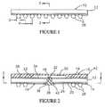
- FIG. 1is an enlarged schematic side elevation view illustrating a semiconductor component constructed in accordance with the invention with adjustable electrical characteristics
- FIG. 2is an enlarged cross sectional view of the component, taken along line 2 — 2 of FIG. 1;
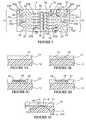
- FIG. 3is a partial, enlarged cross sectional view, taken along line 3 — 3 of FIG. 2, illustrating adjustment circuitry on the component;
- FIG. 3Ais an enlarged cross sectional view, taken along line 3 A— 3 A of FIG. 3, illustrating a substrate and solder mask of the component;
- FIG. 3Bis an enlarged cross sectional view, taken along line 3 B— 3 B of FIG. 3, illustrating a conductor of the component;
- FIG. 3Cis an enlarged cross sectional view, taken along line 3 C— 3 C of FIG. 3, illustrating a wire bonding pad of the component;
- FIG. 3Dis an enlarged cross sectional view, taken along line 3 D— 3 D of FIG. 3, illustrating a bonding pad for a terminal contact of the component;
- FIG. 3Eis an enlarged cross sectional view, taken along line 3 E— 3 E of FIG. 3, illustrating a programmable link of the component;
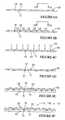
- FIG. 4is an enlarged cross sectional view equivalent to FIG. 3 illustrating adjustment circuitry on an alternate embodiment component having adjustable capacitance characteristics
- FIG. 5is an enlarged cross sectional view equivalent to FIG. 3 illustrating adjustment circuitry on an alternate embodiment component having adjustable inductance characteristics
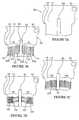
- FIGS. 6A-6Fare schematic cross sectional views illustrating steps in a method for fabricating the semiconductor component
- FIG. 7Ais a view taken along line 7 A— 7 A of FIG. 6A illustrating a leadframe used in the method
- FIG. 7Bis a view taken along line 7 B— 7 B of FIG. 6B illustrating adjustment circuitry on the component of FIG. 4;
- FIG. 7Cis a view equivalent to FIG. 7B illustrating adjustment circuitry on the component of FIG. 4;
- FIG. 7Dis a view taken along line 7 D— 7 D of FIG. 6B illustrating adjustment circuitry on the component of FIG. 5;
- FIGS. 8A and 8Bare schematic cross sectional views equivalent to Figures GB and 6 C respectively, illustrating an alternate embodiment of the fabrication method wherein electronic signals are utilized to program current-type programmable links;
- FIG. 9Ais a schematic plan view of a programmable link in the form of a current fuse configured for use with the fabrication method of FIGS. 8A and 8B;
- FIG. 9Bis a schematic cross sectional view of a programmable link in the form of an anti-fuse configured for use with the fabrication method of FIGS. 8A and 8B;
- FIG. 10Ais a schematic plan view of a multi chip module system constructed using components constructed in accordance with the invention.
- FIG. 10Bis a schematic cross sectional view of a system in a package constructed using components constructed in accordance with the invention.
- semiconductor component 10constructed in accordance with the invention is illustrated.
- semiconductor componentrefers to an element, or to an assembly, that includes a semiconductor die.
- the component 10comprises a board-on-chip (BOC) semiconductor package.
- BOCboard-on-chip
- the semiconductor component 10can comprise another type of semiconductor package such as a chip-on-board (COB) package, a chip scale package (CSP), a BGA device, a flip chip device, or a bumped semiconductor die.
- COBchip-on-board
- CSPchip scale package
- BGAchip scale package
- flip chip devicea bumped semiconductor die.
- the component 10includes a substrate 12 having a first surface 14 (FIG. 2 ), and an opposing second surface 16 (FIG. 2 ).
- the first surface 14 , and the second surface 16are the major planar surfaces of the substrate 12 .
- the substrate 12also includes a wire bonding opening 18 therethrough, extending from the first surface 14 to the second surface 16 .
- the substrate 12includes adjustment circuitry 19 (FIG. 2) formed on the first surface 14 of the substrate 12 , and a die attach area 22 formed on the second surface 16 of the substrate 12 .
- the adjustment circuitry 19includes a pattern of conductors 20 (FIG. 2 ), and programmable links 50 A, 50 B (FIG. 3) in electrical communication with the conductors 20 .
- the conductors 20can comprise a highly conductive metal which is blanket deposited on the substrate 12 , and then etched in required patterns. Alternately, an additive process, such as electroless deposition through a mask, can be used. Suitable metals for the conductors 20 include copper, aluminum, titanium, tungsten, tantalum, platinum, molybdenum, cobalt, nickel, gold, and iridium.
- the substrate 12can comprise an electrically insulating material, such as an organic polymer resin reinforced with glass fibers.
- Suitable materials for the substrate 12include bismaleimide-triazine (BT), epoxy resins (e.g., “FR-4” and “FR-5”), and polyimide resins. These materials can be formed with a desired thickness, and then punched, machined, or otherwise formed with a required peripheral configuration, and with required features.
- a representative thickness of the substrate 12can be from about 0.2 mm to 1.6 mm.
- the substrate 12also includes a solder mask 24 on the first surface 14 , and a solder mask 26 on the second surface 16 .
- the solder masks 24 , 26can comprise a photoimageable dielectric material, such as a negative or positive tone resist.
- the component 10includes an array of terminal contacts 28 on the substrate 12 in electrical communication with integrated circuits, or other electrical elements contained on the component 10 .
- the terminal contacts 28provide separate electrical connection points for transmitting (writing) and receiving (reading) electronic signals from the component 10 .
- the terminal contacts 28provide a structure for bonding the component 10 to a supporting substrate, such as a printed circuit board or module substrate.
- the terminal contacts 28comprise generally spherically shaped contact balls in a ball grid array (BGA), or a fine ball grid array (FBGA).
- BGAball grid array
- FBGAfine ball grid array
- the terminal contacts 28can comprise other conventional contacts having other shapes, and arranged in other patterns, to provide multiple electrical connection points for the component.
- representative contactsinclude bumps, columns, studs, domes, cones, pins and pads.
- the terminal contacts 28can be made of any electrically conductive material, such as a solder alloy, copper, nickel, or a conductive polymer.
- the terminal contacts 28have a diameter “D” and a spacing or pitch “P”.
- a representative range for the diameter Dcan be from about 0.127 mm (0.005 inch) to 0.762 mm (0.030 inch).
- a representative range for the pitch Pcan be from about 0.228 mm (0.008 inch) to 2.0 mm (0.078 inch).
- the component 10also includes a semiconductor die 30 , and a die encapsulant 42 on the die 30 and on the second surface 16 of the substrate 12 .
- the die 30can comprise a conventional semiconductor die having a desired configuration.
- the die 30can comprise a dynamic random access memory (DRAM), a static random access memory (SRAM), a flash memory, a microprocessor, a digital signal processor (DSP), or an application specific integrated circuit (ASIC).
- DRAMdynamic random access memory
- SRAMstatic random access memory
- DSPdigital signal processor
- ASICapplication specific integrated circuit
- the die 30includes a row of bond pads 32 formed on a face portion thereof, in electrical communication with the integrated circuits contained on the die 30 .
- the die 30is bonded face down to the die attach area 22 of the substrate 12 , with the bond pads 32 on the die 30 aligned with the bonding opening 18 in the substrate 12 .
- an adhesive layer 34bonds the die 30 to the die attach area 22 on the substrate 12 .
- the adhesive layer 34can comprise a filled epoxy, an unfilled epoxy, an acrylic, a polyimide or an adhesive tape material.
- wires 36are placed through the wire bonding opening 18 in the substrate 12 , and are wire bonded to the bond pads 32 on the die 30 , and to corresponding wire bonding pads 40 on the substrate 12 .
- a wire bond encapsulant 38fills the wire bonding opening 18 and encapsulates the wires 36 .
- the wire bond encapsulant 38can comprise a polymer material, such as a glob top of epoxy or silicone, deposited in a desired shape using a suitable process such as dispensing through a nozzle, and then cured as required.
- the adjustment circuitry 19also includes terminal contact bonding pads 44 on the substrate 12 configured to provide bonding sites for bonding the terminal contacts 28 to the substrate 12 .
- the terminal contact bonding pads 44are in electrical communication with the conductors 20 and with the wire bonding pads 40 .
- the terminal contact bonding pads 44are in electrical communication with plating conductors 20 P on the substrate 12 that extend to an edge 54 of the substrate 12 .
- the plating conductors 20 Pare initially connected to plating buses, which are used to apply a current to the terminal contact bonding pads 44 , and to the wire bonding pads 40 , for plating non-oxidizing metal layers 46 (FIGS. 3C and 3D) such as gold or platinum layers. These non-oxidizing metal layers 46 facilitate the bonding process for the terminal contacts 28 and the wire bonding process to the die 30 .
- the solder mask 24covers the substrate 12 and the conductors 20 . However, as shown in FIGS. 3C and 3D, the solder mask 24 includes openings 48 aligned with the wire bonding pads 40 and the terminal contact bonding pads 44 .
- the adjustment circuitry 19also includes first programmable links 50 A proximate to the plating conductors 20 P, and second programmable links 50 B between the wire bonding pads 40 and the terminal contact bonding pads 44 .
- programmable linkmeans an element that can be placed in either a first state (short) in which electrical current can be transmitted through the link, or in a second state (open) in which electrical current cannot be transmitted through the link.
- Suitable programmable linksinclude laser fuses, current fuses, laser anti-fuses, and current anti-fuses.
- a laser fuseincludes a segment that can be broken by a laser beam to create an open circuit.
- a voltage fuseincludes a segment that can be broken by application of electrical current having a sufficient amperage to create an open circuit.
- a laser anti-fuseincludes conductive segments separated by a dielectric layer that can be broken down by a laser beam to electrically connect the conductive segments to create a short circuit.
- a current anti fusehas a dielectric layer that can be broken down by application of electrical current having a sufficient amperage to create a short circuit.
- the programmable links 50 A, 50 Bcomprise laser fuses which are initially fabricated in the first state (short), but which can be placed in the second state (open) by application of a laser beam.
- the programmable links 50 A, 50 B in the first state (short)have a continuous line therethrough, whereas the programmable links 50 A, 50 B in the second state (open) do not have a line therethrough.
- the programmable links 50 A, 50 Bcan comprise breakable segments 52 having a width W and a thickness T.
- the width W and the thickness Tcan be selected such that a laser beam of a predetermined power will sever a breakable segment 52 .
- the breakable segments 52can be formed of a same conductive material as the conductors 20 , or can be formed of a different conductive material.
- the breakable segments 52can be aligned with openings 48 in the solder mask 24 to permit access by the laser beam.
- the programmable links 50 Afunction as “trimming links” for trimming portions of the conductors 20 .
- the programmable links 50 Ahave been placed in the second state (open) by application of a laser beam. This removes or “trims” the plating conductors 20 P from the conductors 20 .
- the programmable links 50 Aare illustrated in rows proximate to the outer edges 54 of the substrate 12 . However, each programmable link 50 A can be located as close as possible to a corresponding terminal contact bonding pad 44 , such that as much length of the plating conductors 20 P as is possible can be removed.
- Trimming of the plating conductors 20 Pimproves the integrity of the signals transmitted to and from the terminal contacts 28 (FIG. 2) because the superfluous conductive path through the plating conductors 20 P has been removed.
- the conductors 20are more evenly matched in length, such that their electrical characteristics and signal transmitting capabilities are more evenly matched.
- the programmable links 50 Bfunction as “input/output links” for changing the input/output configuration of the terminal contacts 28 .
- some of the programmable links 50 Bhave been placed in the second state (open) by application of a laser beam, while some of the programmable links 50 B remain in the first state (short).
- the programmable links 50 Ballow selected conductors 20 , and their associated terminal contact bonding pads 44 , to be removed or “trimmed” from the input/output circuit of the component 10 .
- the trimmed conductorsare designated 20 -T. As such, there is no conductive path between a trimmed conductor 20 -T and the die 30 , and no conductive path between the die 30 and the terminal contact 28 (FIG. 2) associated with the trimmed conductor 20 -T. This arrangement permits the input/output configuration of the terminal contacts 28 (FIG. 2) to be changed and customized for a particular application. The electrical configuration of the component 10 can thus be customized as well.
- this arrangementpermits the wire bonding of the die 30 to the conductors 20 to be standardized even for different types of dice.
- a X4 diecan be wire bonded in the same manner as a X16 die, but with the unused terminal contacts 28 taken out of the input/output circuit.
- FIG. 4a cross section equivalent to FIG. 3, of an alternate embodiment component 10 C is illustrated.
- the component 10 Cis constructed substantially as previously described for component 10 (FIG. 1 ), and includes essentially the same elements including adjustment circuitry 19 C.
- the adjustment circuitry 19 Calso includes capacitors 56 in electrical communication with the conductors 20 and the terminal contact bonding pads 44 .
- the adjustment circuitry 19 Cincludes programmable links 50 C in electrical communication with the capacitors 56 .
- the programmable links 50 Ccan comprise laser fuses, current fuses, laser anti-fuses or current anti-fuses, substantially as previously described for programmable links 50 A, 50 B in FIG. 3 .
- the capacitors 56 and programmable links 50 Callow extra capacitance to be added or “trimmed” into the conductors 20 .
- the capacitors 56 and programmable links 50 Cpermit capacitance to be added to the conductive paths through the terminal contacts 28 (FIG. 1) such that the capacitance of individual terminal contacts 28 , and the capacitance of selected groups of the terminal contacts 28 , can be adjusted and/or matched.
- the terminal contacts 28representing matching input/output pin groups for the component 10 C can be matched.
- the conductors having added capacitanceare designated 20 C. These conductors 20 C are in electrical communication with a programmable link 50 C in the first state (short) such that electrical communication with a capacitor 56 is maintained. The other conductors 20 are in electrical communication with a programmable link 50 C in the second state (open) such that there is no electrical communication with a capacitor 56 .
- the capacitors 56 and the programmable links 50 Care located proximate to the terminal contact bonding pads 44 , and are outside of the conductive paths between the terminal contact bonding pads 44 and the die 30 .
- the capacitors 56can comprise conductive plates separated by dielectric layers configured to provide a desired capacitance C.
- the capacitors 56can be constructed using techniques that are known in the art, such as by deposition and patterning of metal and dielectric layers. Alternately, the capacitors 56 can comprise surface mount devices that are commercially available from various manufacturers.
- the value of the capacitance C of each capacitor 56can be selected as required, with from micro farads ( ⁇ F) to pico farads (pF) being representative.
- the capacitorscan also be used as by-pass filters for filtering transient voltages, power supply noise and spurious signals.
- FIG. 5a cross sectional equivalent to FIG. 3, of an alternate embodiment component 10 I is illustrated.
- the component 10 Iis constructed substantially as previously described for component 10 (FIG. 1 ), and includes essentially the same elements including adjustment circuitry 19 I.
- the adjustment circuitry 19 Ialso includes inductance conductors 20 I in electrical communication with the conductors 20 , and with the terminal contact bonding pads 44 .
- the inductance conductors 20 Iare in electrical communication with programmable links 50 I.
- Each inductance conductor 20 I and associated programmable link 50 Iforms an adjustable conductive loop that can be either by-passed, or added, depending on the state of the programmable link 50 I.
- the programmable links 50 Ican comprise laser fuses, current fuses, laser anti-fuses or current anti-fuses, substantially as previously described for programmable links 50 A, 50 B in FIG. 3 .
- the inductance conductors 20 I and programmable links 50 Iallow extra inductance and resistance to be added or “trimmed” into the conductors 20 .
- the inductance conductors 20 I in electrical communication with the programmable links 50 I in the second state (open)are activated, whereas the inductance conductors 20 I in electrical communication with the programmable links in the first state (short) are bypassed.
- each conductor 20 I and programmable links 50 Iare located between the terminal contact bonding pads 44 and the wire bonding pads 40 .
- each conductor 20includes three separate inductance conductors 20 I and programmable links 50 I.
- this arrangementis merely exemplary and other arrangements are possible.
- FIGS. 6A-6Fsteps in a method for fabricating the component 10 , 10 C or 10 I are illustrated.
- a panel 58 containing multiple substrates 12is initially provided.
- the panel 58is similar in function to a semiconductor leadframe, permitting the fabrication of multiple components 10 , 10 C or 10 I at the same time.
- the panel 58includes circular indexing openings 62 proximate to the longitudinal edges thereof.
- the indexing openings 62permit the panel 58 to be handled by automated transfer mechanisms associated with chip bonders, wire bonders, molds, and trim machinery.
- the panel 58includes elongated separation openings 60 which facilitate singulation of the substrates 12 on the panel 58 into separate components 10 , 10 C or 10 I.
- the panel 58also includes a wire bonding opening 18 for each substrate 12 .
- the panel 58can be constructed from a commercially produced bi-material core, such as a copper clad bismaleimide-triazine (BT) core, available from Mitsubishi Gas Chemical Corp., Japan.
- a representative weight of the coppercan be from 0.5 oz to 2 oz. per square foot.
- the adjustment circuitry 19is formed on the substrate 12 .
- the adjustment circuitry 19includes the conductors 20 and the programmable links 50 A, 50 B which are laid out substantially as previously described and shown in FIG. 3 .
- the adjustment circuitry 19includes the terminal contact bonding pads 44 , and the wire bonding pads 40 in electrical communication with the conductors 20 .
- the conductors 20can comprise a highly conductive metal layer, which is blanket deposited onto the panel 58 (e.g., electroless or electrolytic plating), and then etched in required patterns. Alternately, an additive process, such as electroless deposition through a mask, can be used. Suitable metals include copper, aluminum, titanium, tungsten, tantalum, platinum, molybdenum, cobalt, nickel, gold, and iridium.
- the terminal contact bonding pads 44 , and the wire bonding pads 40can be formed at the same time, and using the same process, as for the conductors 20 .
- the non-oxidizing layers 46(FIGS. 3C, 3 D) can be formed on the terminal contact bonding pads 44 , and the wire bonding pads 40 using a plating process, such as electrolytic deposition.
- plating buses 64can be used to electrically connect the conductors 20 for performing the plating process. These plating buses 64 will be trimmed away during the singulating step to be hereinafter described.
- the programmable links 50 A, 50 Bcan be formed at the same time and using the same process as for the conductors 20 .
- the programmable links 50 A, 50 Bcan comprise segments of the conductors 20 formed by etching a blanket deposited layer using an etch mask, or by depositing metal in a required pattern using a deposition mask.
- the programmable links 50 A, 50 Bcan comprise surface mounted devices placed in electrical communication with the conductors 20 .
- the solder mask 24(FIG. 3 B), and the solder mask 26 (FIG. 2) can be formed.
- the solder mask 24includes the openings 48 (FIGS. 3C and 3D) for the terminal contact bonding pads 40 , the wire bonding pads 44 and the programmable links 50 A, 50 B.
- the solder mask 26includes a die sized opening on the die attach area 22 (FIG. 2 ).
- the solder masks 24 , 26can comprise a photoimageable dielectric material, such as a negative or positive tone resist.
- One suitable resistis commercially available from Taiyo America, Inc., Carson City, Nev. under the trademark “PSR-4000”.
- the “PSR-4000” resistcan be mixed with an epoxy such as epoxy “720” manufactured by Ciba-Geigy (e.g., 80% PSR-4000 and 20% epoxy “720”). Another suitable resist is commercially available from Shipley under the trademark “XP-9500”.
- the adjustment circuitry 19 Ccan be configured as previously described and shown in FIG. 4, with capacitors 56 and programmable links 50 C.
- the capacitors 56can comprise etched or deposited metal and dielectric layers formed substantially as previously described for the conductors 20 . Alternately, the capacitors 56 can comprise surface mounted devices placed in electrical communication with the conductors 20 .
- the programmable links 50 Ccan be formed substantially as previously described for programmable links 50 A, 50 B.
- the adjustment circuitry 19 Ican also be configured as previously described and shown in FIG. 5, with inductance conductors 20 I and programmable links 50 I.
- the inductance conductors 20 Ican comprise etched or deposited metal layers formed substantially as previously described for the conductors 20 .
- the programmable links 50 Ican be formed substantially as previously described for programmable links 50 A, 50 B.
- a laser beam 66can be used to place selected programmable links 50 A, 50 B (FIG. 7 B), 50 C (FIG. 7C) or 50 I (FIG. 7 D), in the open state such that no current can be transmitted therethrough.
- Suitable laser systems for laser severing the breakable segments 52 (FIG. 3E) of the programmable links 50 A, 50 Bare manufactured by Electro Scientific, Inc., of Portland, Oreg. as well as others.
- programmable links 50 A, 50 B, 50 C, 50 Iare illustrated as being laser fuses, it is to be understood that these programmable links can also be configured as laser anti-fuses. In this case the laser beam 66 would be used to place selected programmable links in the short state, such that current can be conducted therethrough.
- the die 30can be attached to the substrate 12 using conventional adhesives and die attach systems.
- the die 30can be wire bonded to the wire bonding pads 40 (FIG. 3) using conventional wire bonding equipment.
- the die encapsulant 42can be formed on the die 30 .
- the die encapsulant 42can comprise a deposited or molded polymer.
- the die encapsulant 42can comprise a Novolac based epoxy formed in a desired shape using a transfer molding process, and then cured using an oven.
- the wire bond encapsulant 38is not shown.
- the wire bond encapsulant 38can be formed using a suitable technique such as dispensing and curing a glob top polymer.
- the terminal contacts 28can be formed on the terminal contact bonding pads 44 using a bonding process, such as solder reflow of pre-formed balls, or a deposition process such as electroless deposition of metal bumps.
- a singulation stepcan be performed to singulate the components 10 , 10 C or 10 I from the panel 58 .
- the singulation stepcan be performed using a saw, a shear or another singulation apparatus.
- the singulation stepalso trims the plating buses 64 (FIG. 7B) such that the conductors 20 are no longer electrically connected to one another.
- FIGS. 8A-8B and 9 A- 9 Ban alternate embodiment of the fabrication method illustrated in FIGS. 6A-6F is illustrated.
- an adjustment circuit 19 Sis formed on the substrate 12 , substantially as previously described and shown in FIG. 6 for adjustment circuit 19 .
- the adjustment circuit 19 Sincludes programmable links 50 S (FIG. 9A) configured as current fuses, or alternately programmable links 50 AF configured as anti-fuses.
- each programmable link 50 Sincludes a necked down portion 72 (FIG. 9A) configured to blow, and form an open circuit upon application of a sufficient current.
- each programmable link 50 AFincludes a pair of conductive plates 74 A, 74 B separated by a dielectric layer 76 . Upon application of a sufficient current, the dielectric layer 76 breaks down, such that electrical communication is established between the conductive plates 74 A, 74 B and a short circuit is formed.
- the programmable link 50 AFconfigured as an anti-fuse the same results can be achieved as with a fuse, provided the state of the link (open or short) is opposite to that of the fuse.
- a programming circuit 70is configured to apply the current signals necessary to place the programmable links 50 S or 50 AF in the required state (i.e., open for programmable link 50 S or short for programmable link 50 AF).
- electrical connectors 68such as “POGO PINS” establish electrical communication between the programming circuit 70 and the programmable links 50 S or 50 AF.
- the electrical connectorscan be constructed to electrically engage the terminal contact bonding pads 44 (FIG. 3 ), the wire bonding pads 40 (FIG. 3) or other connection points on the adjustment circuit 19 S.
- FIGS. 10A and 10Belectronic systems constructed using components 10 , 10 C, 10 I fabricated in accordance with the invention are illustrated.
- the components 10 , 10 C, 10 Ican be used in any system in which semiconductor components as previously defined are used.
- a multi chip module system 80includes a module substrate 82 having an edge connector 84 , and a plurality of conductors 86 in electrical communication with the edge connector 84 .
- the components 10 , 10 C, 10 Ican be flip chip mounted to the module substrate 82 , with the terminal contacts 28 (FIG. 1) thereon in electrical communication with the conductors 86 .
- a system in a package (SIP) 88is constructed with one or more components 10 , 10 C, 10 I.
- This type of packageis also referred to as a multi chip module MCM package.
- the system in a package (SIP) 88can be configured to perform a desired function such as micro processing.
- the system in a package (SIP) 88includes a substrate 90 having terminal leads 92 .
- the components 10 , 10 C, 10 Ican be flip chip mounted to the substrate 90 , with the terminal contacts 28 thereon in electrical communication with the terminal leads 92 .
- the system in a package (SIP) 88also includes a package body 94 encapsulating the components 110 , 10 C, 10 I and the substrate 90 .
Landscapes
- Engineering & Computer Science (AREA)
- Microelectronics & Electronic Packaging (AREA)
- Computer Hardware Design (AREA)
- Power Engineering (AREA)
- Physics & Mathematics (AREA)
- Condensed Matter Physics & Semiconductors (AREA)
- General Physics & Mathematics (AREA)
- Geometry (AREA)
- Semiconductor Integrated Circuits (AREA)
Abstract
Description
Claims (21)
Priority Applications (5)
| Application Number | Priority Date | Filing Date | Title |
|---|---|---|---|
| US10/140,340US6753482B1 (en) | 2002-05-06 | 2002-05-06 | Semiconductor component with adjustment circuitry |
| US10/403,741US7007375B2 (en) | 2002-05-06 | 2003-03-31 | Method for fabricating a semiconductor component |
| US10/745,040US6914275B2 (en) | 2002-05-06 | 2003-12-22 | Semiconductor component with electrical characteristic adjustment circuitry |
| US11/210,562US7257884B2 (en) | 2002-05-06 | 2005-08-24 | Method for fabricating semiconductor component with adjustment circuitry for electrical characteristics or input/output configuration |
| US11/705,962US20070137029A1 (en) | 2002-05-06 | 2007-02-14 | Method for fabricating semiconductor component with adjustment circuit for adjusting physical or electrical characteristics of substrate conductors |
Applications Claiming Priority (1)
| Application Number | Priority Date | Filing Date | Title |
|---|---|---|---|
| US10/140,340US6753482B1 (en) | 2002-05-06 | 2002-05-06 | Semiconductor component with adjustment circuitry |
Related Child Applications (2)
| Application Number | Title | Priority Date | Filing Date |
|---|---|---|---|
| US10/403,741DivisionUS7007375B2 (en) | 2002-05-06 | 2003-03-31 | Method for fabricating a semiconductor component |
| US10/745,040DivisionUS6914275B2 (en) | 2002-05-06 | 2003-12-22 | Semiconductor component with electrical characteristic adjustment circuitry |
Publications (1)
| Publication Number | Publication Date |
|---|---|
| US6753482B1true US6753482B1 (en) | 2004-06-22 |
Family
ID=29269659
Family Applications (5)
| Application Number | Title | Priority Date | Filing Date |
|---|---|---|---|
| US10/140,340Expired - LifetimeUS6753482B1 (en) | 2002-05-06 | 2002-05-06 | Semiconductor component with adjustment circuitry |
| US10/403,741Expired - Fee RelatedUS7007375B2 (en) | 2002-05-06 | 2003-03-31 | Method for fabricating a semiconductor component |
| US10/745,040Expired - LifetimeUS6914275B2 (en) | 2002-05-06 | 2003-12-22 | Semiconductor component with electrical characteristic adjustment circuitry |
| US11/210,562Expired - LifetimeUS7257884B2 (en) | 2002-05-06 | 2005-08-24 | Method for fabricating semiconductor component with adjustment circuitry for electrical characteristics or input/output configuration |
| US11/705,962AbandonedUS20070137029A1 (en) | 2002-05-06 | 2007-02-14 | Method for fabricating semiconductor component with adjustment circuit for adjusting physical or electrical characteristics of substrate conductors |
Family Applications After (4)
| Application Number | Title | Priority Date | Filing Date |
|---|---|---|---|
| US10/403,741Expired - Fee RelatedUS7007375B2 (en) | 2002-05-06 | 2003-03-31 | Method for fabricating a semiconductor component |
| US10/745,040Expired - LifetimeUS6914275B2 (en) | 2002-05-06 | 2003-12-22 | Semiconductor component with electrical characteristic adjustment circuitry |
| US11/210,562Expired - LifetimeUS7257884B2 (en) | 2002-05-06 | 2005-08-24 | Method for fabricating semiconductor component with adjustment circuitry for electrical characteristics or input/output configuration |
| US11/705,962AbandonedUS20070137029A1 (en) | 2002-05-06 | 2007-02-14 | Method for fabricating semiconductor component with adjustment circuit for adjusting physical or electrical characteristics of substrate conductors |
Country Status (1)
| Country | Link |
|---|---|
| US (5) | US6753482B1 (en) |
Cited By (9)
| Publication number | Priority date | Publication date | Assignee | Title |
|---|---|---|---|---|
| US20030207501A1 (en)* | 2002-05-06 | 2003-11-06 | Schoenfeld Aaron M. | Semiconductor component with adjustment circuitry and method of fabrication |
| US20040214372A1 (en)* | 2003-04-07 | 2004-10-28 | Walter Moden | Method for fabricating image sensor semiconductor package |
| US20060006494A1 (en)* | 2003-10-22 | 2006-01-12 | Taiwan Semiconductor Manufacturing Co., Ltd. | Electrically programmable polysilicon fuse with multiple level resistance and programming |
| US20060017134A1 (en)* | 2003-04-17 | 2006-01-26 | Kabushiki Kaisha Toshiba | Input protection circuit preventing electrostatic discharge damage of semiconductor integrated circuit |
| US20060131704A1 (en)* | 2004-12-18 | 2006-06-22 | Carberry Patrick J | Packages for encapsulated semiconductor devices and method of making same |
| US20070209830A1 (en)* | 2006-03-13 | 2007-09-13 | Walton Advanced Engineering, Inc. | Semiconductor chip package having a slot type metal film carrying a wire-bonding chip |
| USD775092S1 (en)* | 2013-10-17 | 2016-12-27 | Vlt, Inc. | Electric terminal |
| USD813182S1 (en)* | 2016-08-02 | 2018-03-20 | Panasonic Intellectual Property Management Co., Ltd. | Semiconductor device |
| USD934821S1 (en)* | 2019-07-24 | 2021-11-02 | Nuvoton Technology Corporation Japan | Semiconductor device |
Families Citing this family (10)
| Publication number | Priority date | Publication date | Assignee | Title |
|---|---|---|---|---|
| JP3839267B2 (en)* | 2001-03-08 | 2006-11-01 | 株式会社ルネサステクノロジ | Semiconductor device and communication terminal device using the same |
| US7425758B2 (en)* | 2006-08-28 | 2008-09-16 | Micron Technology, Inc. | Metal core foldover package structures |
| US8124429B2 (en)* | 2006-12-15 | 2012-02-28 | Richard Norman | Reprogrammable circuit board with alignment-insensitive support for multiple component contact types |
| KR20090041756A (en)* | 2007-10-24 | 2009-04-29 | 삼성전자주식회사 | Printed wiring board with adhesive layer and semiconductor package using same |
| US8251483B2 (en)* | 2009-02-13 | 2012-08-28 | Fujifilm Corporation | Mitigation of shorted fluid ejector units |
| US8901747B2 (en) | 2010-07-29 | 2014-12-02 | Mosys, Inc. | Semiconductor chip layout |
| TWM472946U (en)* | 2013-01-16 | 2014-02-21 | Standard Technology Service Inc | Die package structure |
| KR20170098462A (en)* | 2016-02-22 | 2017-08-30 | 삼성전기주식회사 | Package module and manufaturing method of the same |
| US10490341B2 (en)* | 2017-08-17 | 2019-11-26 | Advanced Semiconductor Engineering, Inc. | Electrical device |
| GB2591498B (en)* | 2020-01-30 | 2022-02-09 | Pragmatic Printing Ltd | A method of connecting circuit elements |
Citations (20)
| Publication number | Priority date | Publication date | Assignee | Title |
|---|---|---|---|---|
| US5132878A (en)* | 1987-09-29 | 1992-07-21 | Microelectronics And Computer Technology Corporation | Customizable circuitry |
| US5200580A (en)* | 1991-08-26 | 1993-04-06 | E-Systems, Inc. | Configurable multi-chip module interconnect |
| US5264729A (en)* | 1992-07-29 | 1993-11-23 | Lsi Logic Corporation | Semiconductor package having programmable interconnect |
| US5301143A (en) | 1992-12-31 | 1994-04-05 | Micron Semiconductor, Inc. | Method for identifying a semiconductor die using an IC with programmable links |
| US5691209A (en)* | 1995-09-14 | 1997-11-25 | Liberkowski; Janusz B. | Lattice interconnect method and apparatus for manufacturing multi-chip modules |
| JPH1079362A (en) | 1996-07-12 | 1998-03-24 | Fujitsu Ltd | Semiconductor device manufacturing method, semiconductor device manufacturing mold, semiconductor device, and mounting method thereof |
| US5920110A (en)* | 1995-09-26 | 1999-07-06 | Lsi Logic Corporation | Antifuse device for use on a field programmable interconnect chip |
| US6008533A (en) | 1997-12-08 | 1999-12-28 | Micron Technology, Inc. | Controlling impedances of an integrated circuit |
| JP2000031185A (en) | 1998-07-10 | 2000-01-28 | Citizen Watch Co Ltd | Manufacture of semiconductor device |
| US6157584A (en) | 1999-05-20 | 2000-12-05 | Advanced Micro Devices, Inc. | Redundancy circuit and method for semiconductor memory |
| US6222212B1 (en)* | 1994-01-27 | 2001-04-24 | Integrated Device Technology, Inc. | Semiconductor device having programmable interconnect layers |
| US6277674B1 (en) | 1998-10-02 | 2001-08-21 | Micron Technology, Inc. | Semiconductor fuses, methods of using the same, methods of making the same, and semiconductor devices containing the same |
| US6323534B1 (en) | 1999-04-16 | 2001-11-27 | Micron Technology, Inc. | Fuse for use in a semiconductor device |
| US6333887B1 (en) | 1998-02-27 | 2001-12-25 | Micron Technology, Inc. | Circuits and methods for selectively coupling redundant elements into an integrated circuit |
| US6348400B1 (en) | 1998-01-22 | 2002-02-19 | Micron Technology, Inc. | Method and apparatus for implementing selected functionality on an integrated circuit device |
| US6391681B1 (en) | 2001-03-16 | 2002-05-21 | Micron Technology, Inc. | Semiconductor component having selected terminal contacts with multiple electrical paths |
| US6425766B1 (en)* | 2000-06-09 | 2002-07-30 | Molex Incorporated | Impedance control in edge card connector systems |
| US6449170B1 (en)* | 2000-08-30 | 2002-09-10 | Advanced Micro Devices, Inc. | Integrated circuit package incorporating camouflaged programmable elements |
| US6506981B1 (en)* | 2000-11-22 | 2003-01-14 | Janusz B. Liberkowski | Interconnect structure having fuse or anti-fuse links between profiled apertures |
| US6528735B1 (en)* | 2001-09-07 | 2003-03-04 | International Business Machines Corporation | Substrate design of a chip using a generic substrate design |
Family Cites Families (19)
| Publication number | Priority date | Publication date | Assignee | Title |
|---|---|---|---|---|
| JPH0369131A (en) | 1989-08-08 | 1991-03-25 | Fujitsu Ltd | Probe for semiconductor integrated circuit test use; manufacture of semiconductor device including test process using same probe |
| US5377124A (en) | 1989-09-20 | 1994-12-27 | Aptix Corporation | Field programmable printed circuit board |
| DE69133311T2 (en) | 1990-10-15 | 2004-06-24 | Aptix Corp., San Jose | Connection substrate with integrated circuit for programmable connection and sample analysis |
| JPH0550146A (en) | 1991-08-20 | 1993-03-02 | Showa Alum Corp | Stretching method and stretcher for metal long material |
| US5345119A (en)* | 1992-09-16 | 1994-09-06 | At&T Bell Laboratories | Continuous-time filter tuning with a delay-locked-loop in mass storage systems or the like |
| JPH07159485A (en) | 1993-12-06 | 1995-06-23 | Hitachi Ltd | Semiconductor device test board |
| JP2925964B2 (en) | 1994-04-21 | 1999-07-28 | 松下電器産業株式会社 | Semiconductor wafer container and method of inspecting semiconductor integrated circuit |
| JP3256626B2 (en) | 1994-05-15 | 2002-02-12 | 株式会社東芝 | Semiconductor device |
| JPH0883825A (en) | 1994-09-09 | 1996-03-26 | Tokyo Electron Ltd | Probe equipment |
| US5937515A (en)* | 1995-04-25 | 1999-08-17 | Johnson; Morgan T. | Reconfigurable circuit fabrication method |
| US5982185A (en) | 1996-07-01 | 1999-11-09 | Micron Technology, Inc. | Direct connect carrier for testing semiconductor dice and method of fabrication |
| US5950070A (en)* | 1997-05-15 | 1999-09-07 | Kulicke & Soffa Investments | Method of forming a chip scale package, and a tool used in forming the chip scale package |
| US6008553A (en)* | 1998-09-18 | 1999-12-28 | Ford Global Technologies, Inc. | Linear motor with negative pressure cooling circuit |
| US6249014B1 (en) | 1998-10-01 | 2001-06-19 | Ramtron International Corporation | Hydrogen barrier encapsulation techniques for the control of hydrogen induced degradation of ferroelectric capacitors in conjunction with multilevel metal processing for non-volatile integrated circuit memory devices |
| US6229227B1 (en)* | 1998-12-28 | 2001-05-08 | Kawasaki Steel Corporation | Programmable-value on-chip passive components for integrated circuit (IC) chips, and systems utilizing same |
| AU2001251144A1 (en) | 2000-03-31 | 2001-10-15 | Advanced Bionics Corporation | High contact count, sub-miniature, fully implantable cochlear prosthesis |
| US6541137B1 (en)* | 2000-07-31 | 2003-04-01 | Motorola, Inc. | Multi-layer conductor-dielectric oxide structure |
| JP2002163900A (en)* | 2000-11-22 | 2002-06-07 | Hitachi Ltd | Semiconductor wafer, semiconductor chip, semiconductor device, and method of manufacturing semiconductor device |
| US6753482B1 (en)* | 2002-05-06 | 2004-06-22 | Micron Technology, Inc. | Semiconductor component with adjustment circuitry |
- 2002
- 2002-05-06USUS10/140,340patent/US6753482B1/ennot_activeExpired - Lifetime
- 2003
- 2003-03-31USUS10/403,741patent/US7007375B2/ennot_activeExpired - Fee Related
- 2003-12-22USUS10/745,040patent/US6914275B2/ennot_activeExpired - Lifetime
- 2005
- 2005-08-24USUS11/210,562patent/US7257884B2/ennot_activeExpired - Lifetime
- 2007
- 2007-02-14USUS11/705,962patent/US20070137029A1/ennot_activeAbandoned
Patent Citations (23)
| Publication number | Priority date | Publication date | Assignee | Title |
|---|---|---|---|---|
| US5132878A (en)* | 1987-09-29 | 1992-07-21 | Microelectronics And Computer Technology Corporation | Customizable circuitry |
| US5200580A (en)* | 1991-08-26 | 1993-04-06 | E-Systems, Inc. | Configurable multi-chip module interconnect |
| US5264729A (en)* | 1992-07-29 | 1993-11-23 | Lsi Logic Corporation | Semiconductor package having programmable interconnect |
| US5301143A (en) | 1992-12-31 | 1994-04-05 | Micron Semiconductor, Inc. | Method for identifying a semiconductor die using an IC with programmable links |
| US6222212B1 (en)* | 1994-01-27 | 2001-04-24 | Integrated Device Technology, Inc. | Semiconductor device having programmable interconnect layers |
| US5691209A (en)* | 1995-09-14 | 1997-11-25 | Liberkowski; Janusz B. | Lattice interconnect method and apparatus for manufacturing multi-chip modules |
| US5920110A (en)* | 1995-09-26 | 1999-07-06 | Lsi Logic Corporation | Antifuse device for use on a field programmable interconnect chip |
| JPH1079362A (en) | 1996-07-12 | 1998-03-24 | Fujitsu Ltd | Semiconductor device manufacturing method, semiconductor device manufacturing mold, semiconductor device, and mounting method thereof |
| US6008533A (en) | 1997-12-08 | 1999-12-28 | Micron Technology, Inc. | Controlling impedances of an integrated circuit |
| US6351040B1 (en) | 1998-01-22 | 2002-02-26 | Micron Technology, Inc. | Method and apparatus for implementing selected functionality on an integrated circuit device |
| US6348400B1 (en) | 1998-01-22 | 2002-02-19 | Micron Technology, Inc. | Method and apparatus for implementing selected functionality on an integrated circuit device |
| US6333887B1 (en) | 1998-02-27 | 2001-12-25 | Micron Technology, Inc. | Circuits and methods for selectively coupling redundant elements into an integrated circuit |
| JP2000031185A (en) | 1998-07-10 | 2000-01-28 | Citizen Watch Co Ltd | Manufacture of semiconductor device |
| US6277674B1 (en) | 1998-10-02 | 2001-08-21 | Micron Technology, Inc. | Semiconductor fuses, methods of using the same, methods of making the same, and semiconductor devices containing the same |
| US6323534B1 (en) | 1999-04-16 | 2001-11-27 | Micron Technology, Inc. | Fuse for use in a semiconductor device |
| US6157584A (en) | 1999-05-20 | 2000-12-05 | Advanced Micro Devices, Inc. | Redundancy circuit and method for semiconductor memory |
| US6425766B1 (en)* | 2000-06-09 | 2002-07-30 | Molex Incorporated | Impedance control in edge card connector systems |
| US6449170B1 (en)* | 2000-08-30 | 2002-09-10 | Advanced Micro Devices, Inc. | Integrated circuit package incorporating camouflaged programmable elements |
| US6506981B1 (en)* | 2000-11-22 | 2003-01-14 | Janusz B. Liberkowski | Interconnect structure having fuse or anti-fuse links between profiled apertures |
| US6391681B1 (en) | 2001-03-16 | 2002-05-21 | Micron Technology, Inc. | Semiconductor component having selected terminal contacts with multiple electrical paths |
| US6392291B1 (en) | 2001-03-16 | 2002-05-21 | Micron Technology, Inc. | Semiconductor component having selected terminal contacts with multiple electrical paths |
| US6537850B1 (en) | 2001-03-16 | 2003-03-25 | Micron Technology, Inc. | Method for fabricating semiconductor components with terminal contacts having alternate electrical paths |
| US6528735B1 (en)* | 2001-09-07 | 2003-03-04 | International Business Machines Corporation | Substrate design of a chip using a generic substrate design |
Non-Patent Citations (1)
| Title |
|---|
| US 6,342,723, 1/2002, Wilford (withdrawn) |
Cited By (29)
| Publication number | Priority date | Publication date | Assignee | Title |
|---|---|---|---|---|
| US7257884B2 (en) | 2002-05-06 | 2007-08-21 | Micron Technology, Inc. | Method for fabricating semiconductor component with adjustment circuitry for electrical characteristics or input/output configuration |
| US20060006551A1 (en)* | 2002-05-06 | 2006-01-12 | Schoenfeld Aaron M | Method for fabricating semiconductor component with adjustment circuitry for electrical characteristics or input/output configuration |
| US20040135253A1 (en)* | 2002-05-06 | 2004-07-15 | Schoenfeld Aaron M. | Semiconductor component with electrical characteristic adjustment circuitry |
| US20070137029A1 (en)* | 2002-05-06 | 2007-06-21 | Schoenfeld Aaron M | Method for fabricating semiconductor component with adjustment circuit for adjusting physical or electrical characteristics of substrate conductors |
| US6914275B2 (en)* | 2002-05-06 | 2005-07-05 | Micron Technology, Inc. | Semiconductor component with electrical characteristic adjustment circuitry |
| US7007375B2 (en) | 2002-05-06 | 2006-03-07 | Micron Technology, Inc. | Method for fabricating a semiconductor component |
| US20030207501A1 (en)* | 2002-05-06 | 2003-11-06 | Schoenfeld Aaron M. | Semiconductor component with adjustment circuitry and method of fabrication |
| US6969632B2 (en) | 2003-04-07 | 2005-11-29 | Micron Technology, Inc. | Method for fabricating image sensor semiconductor package |
| US6917090B2 (en) | 2003-04-07 | 2005-07-12 | Micron Technology, Inc. | Chip scale image sensor package |
| US7215015B2 (en) | 2003-04-07 | 2007-05-08 | Micron Technology, Inc. | Imaging system |
| US20050003579A1 (en)* | 2003-04-07 | 2005-01-06 | Walter Moden | Imaging system |
| US20040214372A1 (en)* | 2003-04-07 | 2004-10-28 | Walter Moden | Method for fabricating image sensor semiconductor package |
| US20080230870A1 (en)* | 2003-04-17 | 2008-09-25 | Kabushiki Kaisha | Input protection circuit preventing electrostatic discharge damage of semiconductor integrated circuit |
| US20060017134A1 (en)* | 2003-04-17 | 2006-01-26 | Kabushiki Kaisha Toshiba | Input protection circuit preventing electrostatic discharge damage of semiconductor integrated circuit |
| US7402888B2 (en)* | 2003-04-17 | 2008-07-22 | Kabushiki Kaisha Toshiba | Input protection circuit preventing electrostatic discharge damage of semiconductor integrated circuit |
| US7602041B2 (en)* | 2003-04-17 | 2009-10-13 | Kabushiki Kaisha Toshiba | Input protection circuit preventing electrostatic discharge damage of semiconductor integrated circuit |
| US20060006494A1 (en)* | 2003-10-22 | 2006-01-12 | Taiwan Semiconductor Manufacturing Co., Ltd. | Electrically programmable polysilicon fuse with multiple level resistance and programming |
| US7332791B2 (en)* | 2003-10-22 | 2008-02-19 | Taiwan Semiconductor Manufacturing Co., Ltd. | Electrically programmable polysilicon fuse with multiple level resistance and programming |
| US20060131704A1 (en)* | 2004-12-18 | 2006-06-22 | Carberry Patrick J | Packages for encapsulated semiconductor devices and method of making same |
| US7956451B2 (en)* | 2004-12-18 | 2011-06-07 | Agere Systems Inc. | Packages for encapsulated semiconductor devices and method of making same |
| US20070209830A1 (en)* | 2006-03-13 | 2007-09-13 | Walton Advanced Engineering, Inc. | Semiconductor chip package having a slot type metal film carrying a wire-bonding chip |
| USD775092S1 (en)* | 2013-10-17 | 2016-12-27 | Vlt, Inc. | Electric terminal |
| USD775093S1 (en)* | 2013-10-17 | 2016-12-27 | Vlt, Inc. | Electric terminal |
| USD798249S1 (en)* | 2013-10-17 | 2017-09-26 | Vlt, Inc. | Electric terminal |
| USD834548S1 (en) | 2013-10-17 | 2018-11-27 | Vlt, Inc. | Electric terminal |
| USD877708S1 (en) | 2013-10-17 | 2020-03-10 | Vlt, Inc. | Electrical terminal |
| USD942406S1 (en) | 2013-10-17 | 2022-02-01 | Vicor Corporation | Electric terminal |
| USD813182S1 (en)* | 2016-08-02 | 2018-03-20 | Panasonic Intellectual Property Management Co., Ltd. | Semiconductor device |
| USD934821S1 (en)* | 2019-07-24 | 2021-11-02 | Nuvoton Technology Corporation Japan | Semiconductor device |
Also Published As
| Publication number | Publication date |
|---|---|
| US7257884B2 (en) | 2007-08-21 |
| US6914275B2 (en) | 2005-07-05 |
| US20030207501A1 (en) | 2003-11-06 |
| US20040135253A1 (en) | 2004-07-15 |
| US20070137029A1 (en) | 2007-06-21 |
| US7007375B2 (en) | 2006-03-07 |
| US20060006551A1 (en) | 2006-01-12 |
Similar Documents
| Publication | Publication Date | Title |
|---|---|---|
| US20070137029A1 (en) | Method for fabricating semiconductor component with adjustment circuit for adjusting physical or electrical characteristics of substrate conductors | |
| KR100452819B1 (en) | Chip scale package and method of fabricating the same | |
| US7253022B2 (en) | Method for fabricating semiconductor package with multi-layer metal bumps | |
| US7041537B2 (en) | Method for fabricating semiconductor component with on board capacitor | |
| US6469370B1 (en) | Semiconductor device and method of production of the semiconductor device | |
| US6582992B2 (en) | Stackable semiconductor package and wafer level fabrication method | |
| US4975765A (en) | Highly integrated circuit and method for the production thereof | |
| JPH0220848Y2 (en) | ||
| US6889429B2 (en) | Method of making a lead-free integrated circuit package | |
| US6596560B1 (en) | Method of making wafer level packaging and chip structure | |
| US20020070446A1 (en) | Semiconductor device and method for the production thereof | |
| JP2008172267A (en) | Integrated circuit package manufacturing method and integrated circuit package | |
| EP0843357B1 (en) | Method of manufacturing a grid array semiconductor package | |
| US20100075462A1 (en) | Method of forming semiconductor package | |
| GB2370414A (en) | Method of manufacturing integrated circuit package with cavity to expose lower conductive level | |
| US7198965B2 (en) | Method for making a neo-layer comprising embedded discrete components | |
| US6479306B1 (en) | Method for manufacturing semiconductor device | |
| KR100199286B1 (en) | Chip Scale Package with Grooved Printed Circuit Board | |
| WO1999026288A1 (en) | Semiconductor device and method for manufacturing the same | |
| KR20010004041A (en) | method of fabricating chip size package | |
| KR20020034217A (en) | Capacitor loading type chip scale package and semiconductor module using the same |
Legal Events
| Date | Code | Title | Description |
|---|---|---|---|
| AS | Assignment | Owner name:MICRON TECHNOLOGY, INC., IDAHO Free format text:ASSIGNMENT OF ASSIGNORS INTEREST;ASSIGNORS:SCHOENFELD, AARON M.;CORISIS, DAVID J.;GOMM, TYLER J.;REEL/FRAME:012888/0023;SIGNING DATES FROM 20020412 TO 20020416 | |
| FEPP | Fee payment procedure | Free format text:PAYOR NUMBER ASSIGNED (ORIGINAL EVENT CODE: ASPN); ENTITY STATUS OF PATENT OWNER: LARGE ENTITY | |
| STCF | Information on status: patent grant | Free format text:PATENTED CASE | |
| FPAY | Fee payment | Year of fee payment:4 | |
| FPAY | Fee payment | Year of fee payment:8 | |
| FPAY | Fee payment | Year of fee payment:12 | |
| AS | Assignment | Owner name:U.S. BANK NATIONAL ASSOCIATION, AS COLLATERAL AGENT, CALIFORNIA Free format text:SECURITY INTEREST;ASSIGNOR:MICRON TECHNOLOGY, INC.;REEL/FRAME:038669/0001 Effective date:20160426 Owner name:U.S. BANK NATIONAL ASSOCIATION, AS COLLATERAL AGEN Free format text:SECURITY INTEREST;ASSIGNOR:MICRON TECHNOLOGY, INC.;REEL/FRAME:038669/0001 Effective date:20160426 | |
| AS | Assignment | Owner name:MORGAN STANLEY SENIOR FUNDING, INC., AS COLLATERAL AGENT, MARYLAND Free format text:PATENT SECURITY AGREEMENT;ASSIGNOR:MICRON TECHNOLOGY, INC.;REEL/FRAME:038954/0001 Effective date:20160426 Owner name:MORGAN STANLEY SENIOR FUNDING, INC., AS COLLATERAL Free format text:PATENT SECURITY AGREEMENT;ASSIGNOR:MICRON TECHNOLOGY, INC.;REEL/FRAME:038954/0001 Effective date:20160426 | |
| AS | Assignment | Owner name:U.S. BANK NATIONAL ASSOCIATION, AS COLLATERAL AGENT, CALIFORNIA Free format text:CORRECTIVE ASSIGNMENT TO CORRECT THE REPLACE ERRONEOUSLY FILED PATENT #7358718 WITH THE CORRECT PATENT #7358178 PREVIOUSLY RECORDED ON REEL 038669 FRAME 0001. ASSIGNOR(S) HEREBY CONFIRMS THE SECURITY INTEREST;ASSIGNOR:MICRON TECHNOLOGY, INC.;REEL/FRAME:043079/0001 Effective date:20160426 Owner name:U.S. BANK NATIONAL ASSOCIATION, AS COLLATERAL AGEN Free format text:CORRECTIVE ASSIGNMENT TO CORRECT THE REPLACE ERRONEOUSLY FILED PATENT #7358718 WITH THE CORRECT PATENT #7358178 PREVIOUSLY RECORDED ON REEL 038669 FRAME 0001. ASSIGNOR(S) HEREBY CONFIRMS THE SECURITY INTEREST;ASSIGNOR:MICRON TECHNOLOGY, INC.;REEL/FRAME:043079/0001 Effective date:20160426 | |
| AS | Assignment | Owner name:JPMORGAN CHASE BANK, N.A., AS COLLATERAL AGENT, ILLINOIS Free format text:SECURITY INTEREST;ASSIGNORS:MICRON TECHNOLOGY, INC.;MICRON SEMICONDUCTOR PRODUCTS, INC.;REEL/FRAME:047540/0001 Effective date:20180703 Owner name:JPMORGAN CHASE BANK, N.A., AS COLLATERAL AGENT, IL Free format text:SECURITY INTEREST;ASSIGNORS:MICRON TECHNOLOGY, INC.;MICRON SEMICONDUCTOR PRODUCTS, INC.;REEL/FRAME:047540/0001 Effective date:20180703 | |
| AS | Assignment | Owner name:MICRON TECHNOLOGY, INC., IDAHO Free format text:RELEASE BY SECURED PARTY;ASSIGNOR:U.S. BANK NATIONAL ASSOCIATION, AS COLLATERAL AGENT;REEL/FRAME:047243/0001 Effective date:20180629 | |
| AS | Assignment | Owner name:MICRON TECHNOLOGY, INC., IDAHO Free format text:RELEASE BY SECURED PARTY;ASSIGNOR:MORGAN STANLEY SENIOR FUNDING, INC., AS COLLATERAL AGENT;REEL/FRAME:050937/0001 Effective date:20190731 | |
| AS | Assignment | Owner name:MICRON TECHNOLOGY, INC., IDAHO Free format text:RELEASE BY SECURED PARTY;ASSIGNOR:JPMORGAN CHASE BANK, N.A., AS COLLATERAL AGENT;REEL/FRAME:051028/0001 Effective date:20190731 Owner name:MICRON SEMICONDUCTOR PRODUCTS, INC., IDAHO Free format text:RELEASE BY SECURED PARTY;ASSIGNOR:JPMORGAN CHASE BANK, N.A., AS COLLATERAL AGENT;REEL/FRAME:051028/0001 Effective date:20190731 |