US6751686B2 - Automated transfer of a data unit comprising a plurality of fundamental data units between a host device and a storage medium - Google Patents
Automated transfer of a data unit comprising a plurality of fundamental data units between a host device and a storage mediumDownload PDFInfo
- Publication number
- US6751686B2 US6751686B2US10/094,576US9457602AUS6751686B2US 6751686 B2US6751686 B2US 6751686B2US 9457602 AUS9457602 AUS 9457602AUS 6751686 B2US6751686 B2US 6751686B2
- Authority
- US
- United States
- Prior art keywords
- data
- value
- buffer
- storage medium
- register
- Prior art date
- Legal status (The legal status is an assumption and is not a legal conclusion. Google has not performed a legal analysis and makes no representation as to the accuracy of the status listed.)
- Expired - Lifetime, expires
Links
Images


Classifications
- G—PHYSICS
- G06—COMPUTING OR CALCULATING; COUNTING
- G06F—ELECTRIC DIGITAL DATA PROCESSING
- G06F13/00—Interconnection of, or transfer of information or other signals between, memories, input/output devices or central processing units
- G06F13/38—Information transfer, e.g. on bus
- G06F13/40—Bus structure
- G06F13/4004—Coupling between buses
- G06F13/4027—Coupling between buses using bus bridges
- G06F13/405—Coupling between buses using bus bridges where the bridge performs a synchronising function
- G06F13/4059—Coupling between buses using bus bridges where the bridge performs a synchronising function where the synchronisation uses buffers, e.g. for speed matching between buses
Definitions
- the present inventionrelates to data transfers between a host device and a storage medium.
- Memory controllersare used for transferring data between a host device and a non-volatile semiconductor memory device.
- a single data transfer cycle between the host device and the memory deviceis referred to as a data phase.
- the completion of a host device's request to transfer datamay involve multiple data phases.
- the completion of a data phaserequires a memory controller to perform actions that are in accordance with a host interface protocol.
- Some host interface protocolsallow the exchange of data using data phases comprising relatively large data units (e.g., blocks) that are multiples of the basic fundamental data unit (e.g., sector) used by the memory device for storing data.
- the implementation of a data phase comprising these relatively larger data unitshas traditionally required intervention of the controller microprocessor after the transfer of each fundamental unit contained in a larger data unit.
- each read or write operationmay comprise a large number of fundamental units, such read or write operation may require a large number of microprocessor interventions.
- a large number of microprocessor interventionsis time consuming and can therefore increase the time needed to complete a read or write operation in connection with the memory device.
- This problemmay be alleviated by employing a faster microprocessor.
- Such solutionmay not be very cost effective. Therefore there exists a need for systems and methods for solving these and other problems associated with transferring data between a host and device and a memory device.
- the present inventionrelates to systems and methods for transferring data between a host device and a storage medium.
- an embodiment of one such methodincludes receiving from the host device a command to transfer data between the host device and a storage medium, storing in a first register a value that is correlated to a number of second data units contained in a first data unit, and storing in a second register a value for tracking a number of second data units that are transferred between the host device and a buffer.
- An embodiment of a system for transferring data between a host device and a storage mediumincludes a host interface that receives from the host device a command to transfer data between the host device and a storage medium, a buffer that temporarily stores data that is transferred between the host device and the storage medium, a first register that stores a value that is correlated to a number of second data units contained in a first data unit, and a second register that stores a value for tracking a number of second data units that are transferred between the host device and the buffer.
- FIG. 1is a block diagram of a computer network 100 in accordance with one embodiment of the present invention.
- FIG. 2is a block diagram depicting an embodiment of the data transfer system depicted in FIG. 1 .
- FIG. 3is a flow chart depicting a method that may be implemented by the data transfer system depicted in FIG. 2 .
- FIG. 4is a block diagram depicting an embodiment of the host interface of the data transfer system depicted in FIG. 2 .
- FIG. 5is a block diagram depicting an embodiment of the data mover of the data transfer system depicted in FIG. 2 .
- FIG. 6is a block diagram depicting an embodiment of the storage medium interface of the data transfer system depicted in FIG. 2 .
- FIGS. 7A, 7 B, and 7 Care flow charts depicting a non-limiting example of a method for writing data to the storage medium depicted in FIG. 1 in accordance with an embodiment of the present invention.
- FIGS. 8A, 8 B, and 8 Care flow charts depicting a non-limiting example of a method for reading data from the storage medium depicted in FIG. 1 in accordance with an embodiment of the present invention.
- FIG. 1is a block diagram of a computer network 100 in accordance with one embodiment of the present invention.
- the computer network 100comprises a host 102 and a storage medium (SM) 104 that are coupled to a data transfer system (DTS) 200 .
- DTSdata transfer system
- the Storage Medium 104 and/or the Data Transfer System 200may be part of the host 102 .
- the Data Transfer System 200facilitates read and write data transfers between the host 102 and the Storage Medium 104 . For example, in a write operation, data is transferred from the host 102 to the Storage Medium 104 via the Data Transfer System 200 . Similarly, in a read operation, data is transferred from the Storage Medium 104 to the host 102 via the Data Transfer System 200 .
- the host 102is a data processing system such as, for example, a desktop computer, a notebook computer, a personal digital assistant (PDA), or a mainframe computer, among others.
- the Storage Medium 104is preferably a non-volatile semiconductor memory device such as, for example, flash memory, non-volatile random access memory (non-volatile RAM), or electrically erasable programmable read only memory (EEPROM), among others.
- FIG. 2is a block diagram depicting one embodiment of the Data Transfer System 200 (FIG. 1 ).
- the Data Transfer System 200includes a data mover (DM) module 500 , a host interface (HI) module 400 , a storage medium interface (SMI) module 600 , a buffer 205 (preferably a circular buffer), a microprocessor 201 , memory 202 , and a bus 204 .
- the components of the Data Transfer System 200may be coupled as follows: the Data Mover 500 is coupled to the Host Interface 400 and to the Storage Medium Interface 600 ; the Host Interface 400 is coupled to a host 102 (FIG. 1 ); the Storage Medium Interface 600 is coupled to a Storage Medium 104 (FIG.
- the microprocessor 201is coupled to the memory 202 ; and the Host Interface 400 , the Data Mover 500 , and the Storage Medium Interface 600 are coupled to the microprocessor 201 via the bus 204 .
- the Data Mover 500organizes and controls the flow of data between the host 102 and the Storage Medium 104 .
- the buffer 205is used to buffer data being transferred between the host 102 and the Storage Medium 104 .
- the memory 202is used for storing a data transfer program 203 that is executed by a microprocessor 201 to control the operation of the Host Interface 400 , the Data Mover 500 , and the Storage Medium Interface 600 .
- the memory 202comprises random access memory (RAM) and read only memory (ROM), and the data transfer program 203 comprises firmware.
- the buffer 205 , the Host Interface 400 , the Data Mover 500 , the Storage Medium Interface 600 , the microprocessor 201 , the memory 202 , and the bus 204are preferably, but not necessarily, part of a single application specific integrated circuit (ASIC).
- ASICapplication specific integrated circuit
- FIG. 3depicts a flow chart that illustrates a method 300 that may be implemented by the Data Transfer System 200 (FIG. 2) in accordance with one embodiment of the invention.
- the Data Transfer System 200receives a read or write command from the host 102 (FIG. 1) requesting a read or write operation, respectively.
- the microprocessor 201(FIG. 2) loads registers in the Host Interface 400 , the Data Mover 500 , and the Storage Medium Interface 600 (FIG. 2) for executing the read or write operation requested by the command.
- a read operationdata is transferred from the Storage Medium 104 (FIG. 1) to the host 102 .
- During a write operationdata is transferred from the host 102 to the Storage Medium 104 .
- a data unit(e.g., a block or a sector of data) is transferred between the Data Transfer System 200 and the host 102 or the Storage Medium 104 , as indicated in step 303 .
- the data transferis coordinated and managed by the Host Interface 400 , the Data Mover 500 , and/or the Storage Medium Interface 600 .
- Data that is transferred between the host 102 and the Storage Medium 104is buffered in the buffer 205 of the Data Transfer System 200 .
- a data unit that is transferred between the buffer 205 and the host 102is a block of data that may comprise multiple sectors, whereas a data unit that is transferred between the buffer 205 and the storage medium 104 is a sector (e.g. 512 bytes).
- Datais preferably transferred between the Data Transfer System 200 and the host 102 in units of bytes (8 bits) or words (16 bits), and between the Data Transfer System 200 and the storage medium 104 in units of bytes.
- registers in the Host Interface 400 , the Data Mover 500 , and/or the Storage Medium Interface 600are updated in step 304 to reflect the occurrence of the data transfer.
- FIG. 4is a block diagram illustrating selected components of the Host Interface 400 of the Data Transfer System 200 (FIG. 2) in accordance with one embodiment of the present invention.
- the Host Interface 400interfaces with the host 102 (FIG. 1) and facilitates data transfers between the host 102 and the buffer 205 (FIG. 2 ).
- the Host Interface 400 and the Data Mover 500(FIG. 5) transmit signals to each other in order to indicate their respective status and their readiness to perform a certain step. For instance, an H_XferBlk signal 403 from the Data Mover 500 to the Host Interface 400 indicates that the buffer 205 is ready to provide or receive data to/from the host 102 . On the other hand, an H_BlkXferred signal 404 from the Host Interface 400 to the Data Mover 500 indicates that a block of data has been transferred between the buffer 205 and the host 102 .
- the Host Interface 400includes a WordsPerBlk register 401 that is loaded at the beginning of a read or write operation with the number of words per block of data.
- a WordCtr register 402is used for counting down the number of words transferred during each block transfer. Prior to each block transfer, the WordCtr register 402 is loaded by receiving a value contained in the WordsPerBlk register 401 .
- the WordsPerBlk register 401is loaded with the number of longwords per block of data, and the WordCtr register 402 is used for counting down the number of longwords transferred during each block transfer.
- FIG. 5is a block diagram depicting selected components of the Data Mover 500 in accordance with one embodiment of the present invention.
- the Data Mover 500includes registers containing information as described in the following table:
- BuffSects 505Number of sectors in the buffer 205 MaxBuffSects 510 Size of the buffer 205 DeviceXferSectCtr Counts number of sectors to be transferred (DXSC) 503 to/from Storage Medium 104
- the registers identified in Table 1are used by the Data Mover 500 to manage the transfer of data between the host 102 and the Storage Medium 104 .
- a data transfer between the host 102 and the Storage Medium 104is initiated in response to the Host Interface 400 receiving a read or write command from the host 102 .
- the Host Interface 400interrupts the microprocessor 201 which loads certain registers of the modules Host Interface 400 , Data Mover 500 , and Storage Medium Interface 600 and then activates them (the modules 400 , 500 , and 600 ).
- the Data Mover 500sends a request for a block of data to the Host Interface 400 (for a write operation) or a request for a sector of data to the Storage Medium Interface 600 (for a read operation).
- a request for a block from the Host Interface 400is achieved by sending an H_XferBlk 403 signal to the Host Interface 400
- a request for a sector from the Storage Medium Interface 600is achieved by sending an SMI_XferSect 508 signal to the Storage Medium Interface 600 .
- the Data Mover 500requests that a sector of data be transmitted from the Storage Medium 104 to the buffer 205 .
- the Data Mover 500performs this request by sending an SMI_XferSect 508 signal to the Storage Medium Interface 600 .
- the Data Mover 500also tracks the progress of the sector transfer by managing the DXSC 503 , which the Data Mover 500 decrements by 1 after each successful sector transfer from the Storage Medium 104 to the buffer 205 . Eventually the DXSC 503 will go to 0, and the Data Mover 500 will stop transmitting data transfer requests to the Storage Medium Interface 600 .
- the Data Mover 500 hardwarewill continue to request that a block of data be transmitted from the host 102 to the buffer 205 by sending an H_XferBlk signal to the Host Interface 400 .
- the Data Mover 500will also track the progress of the transfer by managing the HXSC 502 , which is decremented by the value of SPB after each successful block transfer from the host 102 to the buffer 205 . Eventually the HXSC 502 will go to 0, and the Data Mover 500 will stop transmitting data transfer requests to the Host Interface 400 .
- Data transfers between the data transfer buffer 205 and the Host Interface 400 or Storage Medium Interface 600are preferably in units of longwords (e.g., 4 bytes). As each longword is transferred, Data Mover 500 hardware decrements either the Host_LW_Ctr 513 or the SMI_LW_Ctr 514 depending on whether the transfer is to/from the host 102 or the Storage Medium 104 . In addition, word counters internal to the Host Interface 400 and Storage Medium Interface 600 are decremented.
- the Storage Medium Interface 600At the end of a sector transfer to/from the Storage Medium 104 , the Storage Medium Interface 600 's internal word counter goes to 0, prompting it to send the sector acknowledgment SMI_SectXferred 509 to the Data Mover 500 , which is expecting this signal because its own SMI_LW_Ctr 514 has gone to 0.
- the Data Mover 500 hardwarereloads the SMI_LW_Ctr 514 from the register SMI_LW_PerSect 507 and issues another SMI_XferSect 508 signal to the Storage Medium Interface 600 .
- the internal word counter WordCtr 402 of the Host Interface 400goes to 0, prompting the Host Interface 400 to send the block acknowledgment Host_BlkXferred 404 to the Data Mover 500 which is expecting this signal because its Host_LW_Ctr 513 has also gone to 0. If there are more blocks to be transferred, then upon receipt of the Host_BlkXferred 404 signal, the Data Mover 500 hardware reloads the Host_LW_Ctr 513 from the register Host_LW_PerBlk 506 and issues another Host_XferBlk 403 signal to the Host Interface 400 .
- FIG. 6is a block diagram illustrating selected components of the Storage Medium Interface 600 of the Data Transfer System 200 (FIG. 2) in accordance with one embodiment of the present invention.
- the Storage Medium Interface 600interfaces with Storage Medium 104 (FIG. 1) and transfers data between the buffer 205 (FIG. 2) and the Storage Medium 104 in response to receiving an SMI_XferSect signal 508 from the Data Mover 500 .
- the Storage Medium Interface 600transfers a sector of data between the buffer 205 and the Storage Medium 104 , it transmits an SMI_SectXferred signal 509 to the Data Mover 500 confirming the data transfer.
- Registers contained in the Storage Medium Interface 600include an SMI_XferLen register 601 that indicates the number of data sectors to be transferred and an SMI_XferCtr register 602 that counts down the number of sectors transferred.
- the SMI_XferCtr register 602is loaded with the value contained in the SMI_XferLen register 601 prior to each read or write operation.
- FIGS. 7A, 7 B, and 7 Care flow charts depicting a non-limiting example of a write method that is performed by the Data Transfer System 200 (FIG. 2) in accordance with one embodiment of the present invention.
- the Host Interface 400receives a write command from a host 102 (FIG. 1 ).
- the Host Interface 400interrupts the Microprocessor 201 (FIG.
- step 702loads the number of sectors per block into SectsPerBlk (SPB 504 ), the transfer length in sectors into HostXferSectCtr (HXSC 502 ) and DeviceXferSectCtr (DXSC 503 ), the number of longwords in a sector into SMI_LW_PerSect 507 , and the number of longwords in a block into Host_LW_PerBlk 506 .
- SectsPerBlkSPB 504
- HXSC 502HostXferSectCtr
- DXSC 503DeviceXferSectCtr
- the Microprocessor 201sets BuffSects 505 to MaxBuffSects 510 , sets Host_LW_Ptr 511 and SMI_LW_Ptr 512 to SOB_LW_Ptr 515 , and then activates the modules Host Interface 400 , Data Mover 500 , and Storage Medium Interface 600 (FIG. 2 ).
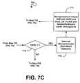
- step 703the Data Mover 500 determines if the amount of data remaining to be transferred is less than a block's worth of data; this determination is based on whether the value of HXSC 502 is less than the value of SPB 504 . If the value of HXSC 502 is less than the value of SPB 504 , then the method 700 proceeds to step 715 (FIG. 7 C).
- the Data Mover 500determines in step 704 if there is at least 1 block's worth of available storage in the buffer 205 ; this determination is based on whether the value of BuffSects 505 is greater than or equal to the value of SPB 504 . If the value of BuffSects 505 is not greater than or equal to the value of SPB 504 , then the method 700 proceeds to step 708 (FIG. 7 B).
- the Data Mover 500sends an H_XferBlk 403 signal to the Host Interface 400 requesting that the Host Interface 400 transfer a block of data from the host 102 to the buffer 205 , as indicated in step 705 .
- the H_XferBlk 403 signalis sent to the Host Interface 400
- a block of datais transferred from the host 102 to the buffer 205 in step 706 and the Data Mover 500 receives an H_BlkXferred 404 signal from the Host Interface 400 confirming the data transfer.
- H_BlkXferred 404 signalis received by the Data Mover 500 from the Host Interface 400 , the values of HXSC 502 and BuffSects 505 are decreased by the value of SPB 504 , as indicated in step 707 .
- the value of Host_LW_Ptr 511is equal to EOB_LW_Ptr 516 , then the value of Host_LW_Ptr 511 is set equal to SOB_LW_Ptr 515 .
- the Data Mover 500determines in step 708 (FIG. 7B) if data sectors remain to be transferred to the Storage Medium 104 (FIG. 1 ); this determination is based on whether the value of DXSC 503 is greater than 0. If the value of DXSC 503 is not greater than 0, then the Storage Medium Interface 600 interrupts the microprocessor 201 in step 709 and the method 700 terminates in step 710 . If, however, the value of DXSC 503 is greater than 0, then the Data Mover 500 determines in step 711 if there is at least one sector of data in the buffer 205 ; this determination is based on whether the value of BuffSects 505 is less than the value of MaxBuffSects 510 .
- the Data Mover 500sends an SMI_XferSect 508 signal to the Storage Medium Interface 600 requesting that the Storage Medium Interface 600 transfer a sector of data from the buffer 205 to the Storage Medium 104 , as indicated in step 712 .
- the method 700returns to step 703 (FIG. 7 A).
- the Storage Medium Interface 600After the Storage Medium Interface 600 receives an SMI_XferSect 508 signal, the Storage Medium Interface 600 transfers a sector of data from the buffer 205 to the Storage Medium 104 , as indicated in step 713 , and then sends an SMI_SectXferred 509 signal to the Data Mover 500 confirming the transfer. After the SMI_SectXferred 509 signal is received by the Data Mover 500 , the value of DXSC 503 is decreased by 1 and the value of BuffSects 505 is increased by 1, as indicated in step 714 .
- SMI_LW_Ptr 512is set equal to SOB_LW_Ptr 515 .
- the Data Mover 500determines if there is a runt block remaining to be transferred.
- a runt blockis an amount of data that is less than the unit of data (e.g. block) that the host 102 uses in sending or receiving data to the Data Transfer System 200 .
- the determination of whether a runt block remains to be transferredis based on whether the value of HXSC 502 is greater than 0. If the value of HXSC 502 is not greater than 0, then the method 700 proceeds to step 708 (FIG. 7 B). If, however, the value of HXSC 502 is greater than 0, then the Data Mover 500 interrupts the microprocessor 201 in step 716 .
- the microprocessor 201After being interrupted, the microprocessor 201 reloads SPB 504 with HXSC 502 and Host_LW_PerBlk 506 with a value equal to the value of HXSC 502 multiplied by the value of SMI_LW_PerSect 507 (i.e. Host_LW_PerBlk 506 is loaded with a value equal to the number of longwords remaining to be transferred).
- the method 700After SPB 504 and Host_LW_PerBlk 506 are reloaded, the method 700 returns to step 703 so that the runt block may be transferred.
- the microprocessor 201reloads SPB 504 and Host_LW_PerBlk 506 with the values that they had prior to when the microprocessor 201 was interrupted in step 716 .
- the microprocessoris not interrupted in step 716 ; instead, SPB 504 and Host_LW_PerBlk 506 are reloaded prior to the runt block transfer using a specialized circuit without microprocessor 201 intervention.
- FIGS. 8A, 8 B, and 8 Care flow charts depicting a non-limiting example of a read method that is performed by the Data Transfer System 200 (FIG. 2) in accordance with one embodiment of the present invention.
- the Host Interface 400receives a read command from a host 102 (FIG. 1 ).
- the Host Interface 400interrupts the microprocessor 201 (FIG.
- step 802loads the number of sectors per block into SPB 504 , the transfer length in sectors into HXSC 502 and DXSC 503 , the number of longwords in a sector into SMI_LW_PerSect 507 , and the number of longwords in a block into Host_LW_PerBlk 506 .
- the Microprocessor 201sets BuffSects 505 to 0, sets Host_LW_Ptr 511 and SMI_LW_Ptr 512 to SOB_LW_Ptr 515 , and then activates the modules Host Interface 400 , Data Mover 500 , and Storage Medium Interface 600 (FIG. 2 ).
- the Data Mover 500determines in step 803 if data sectors are to be received from the Storage Medium 104 (FIG. 1 ); this determination is based on whether the value of DXSC 503 is greater than 0. If the value of DXSC 503 is not greater than 0, then the method 800 proceeds to step 808 (FIG. 8 B). If the value of DXSC 503 is greater than 0, then the Data Mover 500 determines in step 804 if there is space in the buffer 205 for receiving a sector of data from the Storage Medium 104 ; this determination is based on whether the value of BuffSects 505 is less than the value of MaxBuffSects 510 .
- step 808the Data Mover 500 sends an SMI_XferSect 508 signal to the Storage Medium Interface 600 requesting that the Storage Medium Interface 600 transfer a sector of data from the Storage Medium 104 to the buffer 205 , as indicated in step 805 .
- the Storage Medium Interface 600After the Storage Medium Interface 600 receives the SMI_XferSect 508 signal, the Storage Medium Interface 600 transfers a sector of data from the Storage Medium 104 to the buffer 205 , as indicated in step 806 , and then sends an SMI_SectXferred 509 signal to the Data Mover 500 confirming the transfer. After the SMI_SectXferred 509 signal is received by the Data Mover 500 from the Storage Medium Interface 600 , the value of DXSC 503 is decreased by 1 and the value of BuffSects 505 is increased by 1, as indicated in step 807 .
- SMI_LW_Ptr 512is set equal to SOB_LW_Ptr 516 .
- step 808the Data Mover 500 determines if the amount of data remaining to be transferred is less than a block's worth of data. This determination is based on whether the value of HXSC 502 is less than the value of SPB 504 . If the value of HXSC 502 is less than the value of SPB 504 , then the method 800 proceeds to step 815 (FIG. 8 C).
- the Data Mover 500determines in step 809 if there is at least 1 block's worth of data in the buffer 205 ; this determination is based on whether the value of BuffSects 505 is greater than or equal to the value of SPB 504 . If the value of BuffSects 505 is not greater than or equal to the value of SPB 504 , then the method 800 proceeds to step 803 (FIG. 8 A).
- the Data Mover 500sends an H_XferBlk 403 signal to the Host Interface 400 requesting that the Host Interface 400 transfer a block of data from the buffer 205 to the host 102 , as indicated in step 810 .
- the H_XferBlk 403 signalis sent to the Host Interface 400
- a block of datais transferred from the buffer 205 to the host 102 in step 811 and the Data Mover 500 receives an H_BlkXferred 404 signal from the Host Interface 400 confirming the data transfer.
- the values of HXSC 502 and BuffSects 505are decreased by the value of SPB 504 , as indicated in step 812 .
- the value of Host_LW_Ptr 511is equal to EOB_LW_Ptr 516 , then the value of Host_LW_Ptr 511 is set to SOB_LW_Ptr 515 .
- the method 800returns to step 803 (FIG. 8 A).
- the Data Mover 500determines if there is a runt block remaining to be transferred. The determination of whether a runt block remains to be transferred is based on whether the value of HXSC 502 is greater than 0. If the Data Mover 500 determines in step 815 that the value of HXSC 502 is not greater than 0, then the Data Mover 500 interrupts the microprocessor 201 in step 818 and the method 800 terminates in step 819 . If, however, the value of HXSC 502 is greater than 0, then the Data Mover 500 interrupts the microprocessor 201 in step 816 .
- the microprocessor 201After being interrupted, the microprocessor 201 reloads SPB 504 with HXSC 502 and reloads Host_LW_PerBlk 506 with a value equal to the value of HXSC 502 multiplied by the value of SMI_LW_PerSect 507 (i.e., Host_LW_PerBlk 506 is loaded with a value equal to the number of longwords remaining to be transferred). After SPB 504 and Host_LW_PerBlk 506 are reloaded, the method 800 returns to step 808 so that the runt block may be transferred.
- the microprocessor 201reloads SPB 504 and Host_LW_PerBlk 506 with the values that they had prior to when the microprocessor 201 was interrupted in step 816 .
- the microprocessoris not interrupted in step 816 . Instead, SPB 504 and Host_LW_PerBlk 506 are reloaded prior to the runt block transfer using a specialized circuit without microprocessor 201 intervention.
Landscapes
- Engineering & Computer Science (AREA)
- General Engineering & Computer Science (AREA)
- Theoretical Computer Science (AREA)
- Computer Hardware Design (AREA)
- Physics & Mathematics (AREA)
- General Physics & Mathematics (AREA)
- Information Transfer Systems (AREA)
Abstract
Description
| TABLE 1 |
| Registers that may be included in the |
| REGISTER NAME | CONTENT/ |
| Host_LW_Ptr | |
| 511 | |
| transfers to/from | |
| Long word counter for transfers to/from | |
| Host_LW_PerBlk 506 | The number of long words per block of data |
| HostXferSectCtr | Counts number of sectors to be transferred |
| (HXSC) 502 | to/from |
| SectsPerBlk (SPB) 504 | Number of sectors per block of |
| SOB_LW_Ptr | |
| 515 | Start address of |
| EOB_LW_Ptr 516 | End address of |
| to/from | |
| Long word counter for transfers to/from | |
| The number of long words per sector. | |
| Number of sectors in the | |
| Size of the | |
| DeviceXferSectCtr | Counts number of sectors to be transferred |
| (DXSC) 503 | to/from |
Claims (22)
Priority Applications (1)
| Application Number | Priority Date | Filing Date | Title |
|---|---|---|---|
| US10/094,576US6751686B2 (en) | 2002-03-08 | 2002-03-08 | Automated transfer of a data unit comprising a plurality of fundamental data units between a host device and a storage medium |
Applications Claiming Priority (1)
| Application Number | Priority Date | Filing Date | Title |
|---|---|---|---|
| US10/094,576US6751686B2 (en) | 2002-03-08 | 2002-03-08 | Automated transfer of a data unit comprising a plurality of fundamental data units between a host device and a storage medium |
Publications (2)
| Publication Number | Publication Date |
|---|---|
| US20030172203A1 US20030172203A1 (en) | 2003-09-11 |
| US6751686B2true US6751686B2 (en) | 2004-06-15 |
Family
ID=29548137
Family Applications (1)
| Application Number | Title | Priority Date | Filing Date |
|---|---|---|---|
| US10/094,576Expired - LifetimeUS6751686B2 (en) | 2002-03-08 | 2002-03-08 | Automated transfer of a data unit comprising a plurality of fundamental data units between a host device and a storage medium |
Country Status (1)
| Country | Link |
|---|---|
| US (1) | US6751686B2 (en) |
Cited By (12)
| Publication number | Priority date | Publication date | Assignee | Title |
|---|---|---|---|---|
| US20040010678A1 (en)* | 2002-07-09 | 2004-01-15 | Lsi Logic Corporation | Method and/or apparatus for implementing enhanced device identification |
| US7539924B1 (en) | 2005-11-15 | 2009-05-26 | Western Digital Technologies, Inc. | Disk drive implementing data path protection by encoding large host blocks into sub blocks |
| US20110119464A1 (en)* | 2009-11-13 | 2011-05-19 | Western Digital Technologies, Inc. | Data storage system comprising a mapping bridge for aligning host block size with physical block size of a data storage device |
| US20110125977A1 (en)* | 2009-11-20 | 2011-05-26 | Karr Christopher P | Aligning data storage device partition to boundary of physical data sector |
| US8006027B1 (en) | 2008-09-11 | 2011-08-23 | Western Digital Technologies, Inc. | Method of staging small writes on a large sector disk drive |
| US8392689B1 (en) | 2010-05-24 | 2013-03-05 | Western Digital Technologies, Inc. | Address optimized buffer transfer requests |
| US8397107B1 (en) | 2009-12-11 | 2013-03-12 | Western Digital Technologies, Inc. | Data storage device employing data path protection using both LBA and PBA |
| US8671250B2 (en) | 2011-12-15 | 2014-03-11 | Western Digital Technologies, Inc. | Data storage device generating redundancy for data path protection of a parity sector |
| US8990493B1 (en) | 2011-06-30 | 2015-03-24 | Western Digital Technologies, Inc. | Method and apparatus for performing force unit access writes on a disk |
| US8996839B1 (en) | 2012-01-23 | 2015-03-31 | Western Digital Technologies, Inc. | Data storage device aligning partition to boundary of sector when partition offset correlates with offset of write commands |
| US9063838B1 (en) | 2012-01-23 | 2015-06-23 | Western Digital Technologies, Inc. | Data storage device shifting data chunks of alignment zone relative to sector boundaries |
| US9106592B1 (en) | 2008-05-18 | 2015-08-11 | Western Digital Technologies, Inc. | Controller and method for controlling a buffered data transfer device |
Citations (5)
| Publication number | Priority date | Publication date | Assignee | Title |
|---|---|---|---|---|
| US5459850A (en)* | 1993-02-19 | 1995-10-17 | Conner Peripherals, Inc. | Flash solid state drive that emulates a disk drive and stores variable length and fixed lenth data blocks |
| US5465338A (en)* | 1993-08-24 | 1995-11-07 | Conner Peripherals, Inc. | Disk drive system interface architecture employing state machines |
| US5644787A (en)* | 1993-08-03 | 1997-07-01 | Seiko Epson Corporation | Apparatus for controlling data transfer between external interfaces through buffer memory using table data having transfer start address transfer count and unit selection parameter |
| US6170031B1 (en)* | 1997-07-08 | 2001-01-02 | Seagate Technology Llc | Read/write state machines for transferring data to/from host interface in a digital data storage system |
| US6421274B1 (en)* | 2001-03-23 | 2002-07-16 | Mitsubishi Denki Kabushiki Kaisha | Semiconductor memory device and reading and writing method thereof |
- 2002
- 2002-03-08USUS10/094,576patent/US6751686B2/ennot_activeExpired - Lifetime
Patent Citations (5)
| Publication number | Priority date | Publication date | Assignee | Title |
|---|---|---|---|---|
| US5459850A (en)* | 1993-02-19 | 1995-10-17 | Conner Peripherals, Inc. | Flash solid state drive that emulates a disk drive and stores variable length and fixed lenth data blocks |
| US5644787A (en)* | 1993-08-03 | 1997-07-01 | Seiko Epson Corporation | Apparatus for controlling data transfer between external interfaces through buffer memory using table data having transfer start address transfer count and unit selection parameter |
| US5465338A (en)* | 1993-08-24 | 1995-11-07 | Conner Peripherals, Inc. | Disk drive system interface architecture employing state machines |
| US6170031B1 (en)* | 1997-07-08 | 2001-01-02 | Seagate Technology Llc | Read/write state machines for transferring data to/from host interface in a digital data storage system |
| US6421274B1 (en)* | 2001-03-23 | 2002-07-16 | Mitsubishi Denki Kabushiki Kaisha | Semiconductor memory device and reading and writing method thereof |
Cited By (16)
| Publication number | Priority date | Publication date | Assignee | Title |
|---|---|---|---|---|
| US7082522B2 (en)* | 2002-07-09 | 2006-07-25 | Lsi Logic Corporation | Method and/or apparatus for implementing enhanced device identification |
| US20040010678A1 (en)* | 2002-07-09 | 2004-01-15 | Lsi Logic Corporation | Method and/or apparatus for implementing enhanced device identification |
| US7539924B1 (en) | 2005-11-15 | 2009-05-26 | Western Digital Technologies, Inc. | Disk drive implementing data path protection by encoding large host blocks into sub blocks |
| US8433977B1 (en) | 2005-11-15 | 2013-04-30 | Western Digital Technologies, Inc. | Storage device implementing data path protection by encoding large host blocks into sub blocks |
| US9106592B1 (en) | 2008-05-18 | 2015-08-11 | Western Digital Technologies, Inc. | Controller and method for controlling a buffered data transfer device |
| US8006027B1 (en) | 2008-09-11 | 2011-08-23 | Western Digital Technologies, Inc. | Method of staging small writes on a large sector disk drive |
| US20110119464A1 (en)* | 2009-11-13 | 2011-05-19 | Western Digital Technologies, Inc. | Data storage system comprising a mapping bridge for aligning host block size with physical block size of a data storage device |
| US8255661B2 (en) | 2009-11-13 | 2012-08-28 | Western Digital Technologies, Inc. | Data storage system comprising a mapping bridge for aligning host block size with physical block size of a data storage device |
| US20110125977A1 (en)* | 2009-11-20 | 2011-05-26 | Karr Christopher P | Aligning data storage device partition to boundary of physical data sector |
| US8285965B2 (en) | 2009-11-20 | 2012-10-09 | Western Digital Technologies, Inc. | Aligning data storage device partition to boundary of physical data sector |
| US8397107B1 (en) | 2009-12-11 | 2013-03-12 | Western Digital Technologies, Inc. | Data storage device employing data path protection using both LBA and PBA |
| US8392689B1 (en) | 2010-05-24 | 2013-03-05 | Western Digital Technologies, Inc. | Address optimized buffer transfer requests |
| US8990493B1 (en) | 2011-06-30 | 2015-03-24 | Western Digital Technologies, Inc. | Method and apparatus for performing force unit access writes on a disk |
| US8671250B2 (en) | 2011-12-15 | 2014-03-11 | Western Digital Technologies, Inc. | Data storage device generating redundancy for data path protection of a parity sector |
| US8996839B1 (en) | 2012-01-23 | 2015-03-31 | Western Digital Technologies, Inc. | Data storage device aligning partition to boundary of sector when partition offset correlates with offset of write commands |
| US9063838B1 (en) | 2012-01-23 | 2015-06-23 | Western Digital Technologies, Inc. | Data storage device shifting data chunks of alignment zone relative to sector boundaries |
Also Published As
| Publication number | Publication date |
|---|---|
| US20030172203A1 (en) | 2003-09-11 |
Similar Documents
| Publication | Publication Date | Title |
|---|---|---|
| US7069373B2 (en) | USB endpoint controller flexible memory management | |
| CN102460405B (en) | Method and system for controlling host memory access by memory device | |
| US5664145A (en) | Apparatus and method for transferring data in a data storage subsystems wherein a multi-sector data transfer order is executed while a subsequent order is issued | |
| EP3470971B1 (en) | Method, apparatus, and system for accessing memory device | |
| US6751686B2 (en) | Automated transfer of a data unit comprising a plurality of fundamental data units between a host device and a storage medium | |
| US8635386B2 (en) | Communication control device, data communication method and program | |
| US11199992B2 (en) | Automatic host buffer pointer pattern detection | |
| WO2021056708A1 (en) | Mass data import method and apparatus, computer device, and storage medium | |
| US7490185B2 (en) | Data processing system, access control method, and access control device | |
| CN101599049B (en) | Method for controlling discontinuous physical addresses of DMA access and DMA controller | |
| US20080225858A1 (en) | Data transferring apparatus and information processing system | |
| US20030172229A1 (en) | Systems and methods for detecting and compensating for runt block data transfers | |
| EP1253520B1 (en) | Apparatus for issuing command for high-speed serial interface | |
| US6745263B2 (en) | Automated multiple data unit transfers between a host device and a storage medium | |
| CN100357920C (en) | Parallel input/output data transmission controller | |
| US7421459B2 (en) | Buffer management for data transfers between a host device and a storage medium | |
| US8392620B2 (en) | Accelerated access apparatus and reading and writing methods thereof | |
| US8769167B2 (en) | Channel device, information processing system and data transfer method | |
| US11537524B2 (en) | Effective PCIe utilization by PCIe TLP coalescing | |
| US20050027906A1 (en) | System and method for adaptive buffer allocation in a memory device interface | |
| US8667188B2 (en) | Communication between a computer and a data storage device | |
| US20240295990A1 (en) | System and Method for searching a buffer of a non-volatile storage Host Controller | |
| US11127466B2 (en) | Read data sorting method and storage device for sequentially transmitting read data of continuous logic block addresses to host | |
| WO1992015058A1 (en) | Data storage subsystem | |
| WO1992015054A1 (en) | Data transfer between a data storage subsystem and host system |
Legal Events
| Date | Code | Title | Description |
|---|---|---|---|
| AS | Assignment | Owner name:HEWLETT-PACKARD COMPANY, COLORADO Free format text:ASSIGNMENT OF ASSIGNORS INTEREST;ASSIGNORS:TAKASUGI, ROBIN ALEXIS;WYATT, STEWART R.;REEL/FRAME:012870/0592 Effective date:20020228 | |
| AS | Assignment | Owner name:HEWLETT-PACKARD DEVELOPMENT COMPANY, L.P., COLORADO Free format text:ASSIGNMENT OF ASSIGNORS INTEREST;ASSIGNOR:HEWLETT-PACKARD COMPANY;REEL/FRAME:013776/0928 Effective date:20030131 Owner name:HEWLETT-PACKARD DEVELOPMENT COMPANY, L.P., COLORAD Free format text:ASSIGNMENT OF ASSIGNORS INTEREST;ASSIGNOR:HEWLETT-PACKARD COMPANY;REEL/FRAME:013776/0928 Effective date:20030131 Owner name:HEWLETT-PACKARD DEVELOPMENT COMPANY, L.P.,COLORADO Free format text:ASSIGNMENT OF ASSIGNORS INTEREST;ASSIGNOR:HEWLETT-PACKARD COMPANY;REEL/FRAME:013776/0928 Effective date:20030131 | |
| STCF | Information on status: patent grant | Free format text:PATENTED CASE | |
| FEPP | Fee payment procedure | Free format text:PAYOR NUMBER ASSIGNED (ORIGINAL EVENT CODE: ASPN); ENTITY STATUS OF PATENT OWNER: LARGE ENTITY | |
| FPAY | Fee payment | Year of fee payment:4 | |
| REMI | Maintenance fee reminder mailed | ||
| AS | Assignment | Owner name:WELLS FARGO BANK, NATIONAL ASSOCIATION, AS COLLATERAL AGENT AND SECOND PRIORITY REPRESENTATIVE, CALIFORNIA Free format text:SECURITY AGREEMENT;ASSIGNORS:MAXTOR CORPORATION;SEAGATE TECHNOLOGY LLC;SEAGATE TECHNOLOGY INTERNATIONAL;REEL/FRAME:022757/0017 Effective date:20090507 Owner name:JPMORGAN CHASE BANK, N.A., AS ADMINISTRATIVE AGENT AND FIRST PRIORITY REPRESENTATIVE, NEW YORK Free format text:SECURITY AGREEMENT;ASSIGNORS:MAXTOR CORPORATION;SEAGATE TECHNOLOGY LLC;SEAGATE TECHNOLOGY INTERNATIONAL;REEL/FRAME:022757/0017 Effective date:20090507 Owner name:JPMORGAN CHASE BANK, N.A., AS ADMINISTRATIVE AGENT Free format text:SECURITY AGREEMENT;ASSIGNORS:MAXTOR CORPORATION;SEAGATE TECHNOLOGY LLC;SEAGATE TECHNOLOGY INTERNATIONAL;REEL/FRAME:022757/0017 Effective date:20090507 Owner name:WELLS FARGO BANK, NATIONAL ASSOCIATION, AS COLLATE Free format text:SECURITY AGREEMENT;ASSIGNORS:MAXTOR CORPORATION;SEAGATE TECHNOLOGY LLC;SEAGATE TECHNOLOGY INTERNATIONAL;REEL/FRAME:022757/0017 Effective date:20090507 | |
| AS | Assignment | Owner name:SEAGATE TECHNOLOGY HDD HOLDINGS, CALIFORNIA Free format text:RELEASE;ASSIGNOR:JPMORGAN CHASE BANK, N.A., AS ADMINISTRATIVE AGENT;REEL/FRAME:025662/0001 Effective date:20110114 Owner name:SEAGATE TECHNOLOGY LLC, CALIFORNIA Free format text:RELEASE;ASSIGNOR:JPMORGAN CHASE BANK, N.A., AS ADMINISTRATIVE AGENT;REEL/FRAME:025662/0001 Effective date:20110114 Owner name:MAXTOR CORPORATION, CALIFORNIA Free format text:RELEASE;ASSIGNOR:JPMORGAN CHASE BANK, N.A., AS ADMINISTRATIVE AGENT;REEL/FRAME:025662/0001 Effective date:20110114 Owner name:SEAGATE TECHNOLOGY INTERNATIONAL, CALIFORNIA Free format text:RELEASE;ASSIGNOR:JPMORGAN CHASE BANK, N.A., AS ADMINISTRATIVE AGENT;REEL/FRAME:025662/0001 Effective date:20110114 | |
| AS | Assignment | Owner name:THE BANK OF NOVA SCOTIA, AS ADMINISTRATIVE AGENT, CANADA Free format text:SECURITY AGREEMENT;ASSIGNOR:SEAGATE TECHNOLOGY LLC;REEL/FRAME:026010/0350 Effective date:20110118 Owner name:THE BANK OF NOVA SCOTIA, AS ADMINISTRATIVE AGENT, Free format text:SECURITY AGREEMENT;ASSIGNOR:SEAGATE TECHNOLOGY LLC;REEL/FRAME:026010/0350 Effective date:20110118 | |
| FPAY | Fee payment | Year of fee payment:8 | |
| AS | Assignment | Owner name:EVAULT INC. (F/K/A I365 INC.), CALIFORNIA Free format text:TERMINATION AND RELEASE OF SECURITY INTEREST IN PATENT RIGHTS;ASSIGNOR:WELLS FARGO BANK, NATIONAL ASSOCIATION, AS COLLATERAL AGENT AND SECOND PRIORITY REPRESENTATIVE;REEL/FRAME:030833/0001 Effective date:20130312 Owner name:SEAGATE TECHNOLOGY INTERNATIONAL, CAYMAN ISLANDS Free format text:TERMINATION AND RELEASE OF SECURITY INTEREST IN PATENT RIGHTS;ASSIGNOR:WELLS FARGO BANK, NATIONAL ASSOCIATION, AS COLLATERAL AGENT AND SECOND PRIORITY REPRESENTATIVE;REEL/FRAME:030833/0001 Effective date:20130312 Owner name:SEAGATE TECHNOLOGY US HOLDINGS, INC., CALIFORNIA Free format text:TERMINATION AND RELEASE OF SECURITY INTEREST IN PATENT RIGHTS;ASSIGNOR:WELLS FARGO BANK, NATIONAL ASSOCIATION, AS COLLATERAL AGENT AND SECOND PRIORITY REPRESENTATIVE;REEL/FRAME:030833/0001 Effective date:20130312 Owner name:SEAGATE TECHNOLOGY LLC, CALIFORNIA Free format text:TERMINATION AND RELEASE OF SECURITY INTEREST IN PATENT RIGHTS;ASSIGNOR:WELLS FARGO BANK, NATIONAL ASSOCIATION, AS COLLATERAL AGENT AND SECOND PRIORITY REPRESENTATIVE;REEL/FRAME:030833/0001 Effective date:20130312 | |
| FPAY | Fee payment | Year of fee payment:12 | |
| AS | Assignment | Owner name:SEAGATE TECHNOLOGY PUBLIC LIMITED COMPANY, CALIFORNIA Free format text:RELEASE BY SECURED PARTY;ASSIGNOR:THE BANK OF NOVA SCOTIA;REEL/FRAME:072193/0001 Effective date:20250303 Owner name:SEAGATE TECHNOLOGY, CALIFORNIA Free format text:RELEASE BY SECURED PARTY;ASSIGNOR:THE BANK OF NOVA SCOTIA;REEL/FRAME:072193/0001 Effective date:20250303 Owner name:SEAGATE TECHNOLOGY HDD HOLDINGS, CALIFORNIA Free format text:RELEASE BY SECURED PARTY;ASSIGNOR:THE BANK OF NOVA SCOTIA;REEL/FRAME:072193/0001 Effective date:20250303 Owner name:I365 INC., CALIFORNIA Free format text:RELEASE BY SECURED PARTY;ASSIGNOR:THE BANK OF NOVA SCOTIA;REEL/FRAME:072193/0001 Effective date:20250303 Owner name:SEAGATE TECHNOLOGY LLC, CALIFORNIA Free format text:RELEASE BY SECURED PARTY;ASSIGNOR:THE BANK OF NOVA SCOTIA;REEL/FRAME:072193/0001 Effective date:20250303 Owner name:SEAGATE TECHNOLOGY INTERNATIONAL, CAYMAN ISLANDS Free format text:RELEASE BY SECURED PARTY;ASSIGNOR:THE BANK OF NOVA SCOTIA;REEL/FRAME:072193/0001 Effective date:20250303 Owner name:SEAGATE HDD CAYMAN, CAYMAN ISLANDS Free format text:RELEASE BY SECURED PARTY;ASSIGNOR:THE BANK OF NOVA SCOTIA;REEL/FRAME:072193/0001 Effective date:20250303 Owner name:SEAGATE TECHNOLOGY (US) HOLDINGS, INC., CALIFORNIA Free format text:RELEASE BY SECURED PARTY;ASSIGNOR:THE BANK OF NOVA SCOTIA;REEL/FRAME:072193/0001 Effective date:20250303 |