US6750079B2 - Method for making programmable resistance memory element - Google Patents
Method for making programmable resistance memory elementDownload PDFInfo
- Publication number
- US6750079B2 US6750079B2US09/891,157US89115701AUS6750079B2US 6750079 B2US6750079 B2US 6750079B2US 89115701 AUS89115701 AUS 89115701AUS 6750079 B2US6750079 B2US 6750079B2
- Authority
- US
- United States
- Prior art keywords
- layer
- forming
- conductive
- sidewall
- conductive layer
- Prior art date
- Legal status (The legal status is an assumption and is not a legal conclusion. Google has not performed a legal analysis and makes no representation as to the accuracy of the status listed.)
- Expired - Lifetime
Links
- 238000000034methodMethods0.000titleclaimsdescription71
- 125000006850spacer groupChemical group0.000claimsabstractdescription119
- 238000004519manufacturing processMethods0.000claimsabstractdescription3
- 239000000463materialSubstances0.000claimsdescription164
- 229910021420polycrystalline siliconInorganic materials0.000claimsdescription43
- 229920005591polysiliconPolymers0.000claimsdescription43
- 238000005530etchingMethods0.000claimsdescription23
- 229920002120photoresistant polymerPolymers0.000claimsdescription14
- 239000012782phase change materialSubstances0.000claimsdescription10
- 239000004065semiconductorSubstances0.000claimsdescription7
- 150000004767nitridesChemical class0.000claimsdescription5
- 229910052798chalcogenInorganic materials0.000claimsdescription4
- 150000001787chalcogensChemical class0.000claimsdescription4
- 239000010410layerSubstances0.000description219
- 239000004020conductorSubstances0.000description29
- VYPSYNLAJGMNEJ-UHFFFAOYSA-NSilicium dioxideChemical compoundO=[Si]=OVYPSYNLAJGMNEJ-UHFFFAOYSA-N0.000description21
- 239000000758substrateSubstances0.000description21
- 238000000151depositionMethods0.000description16
- 238000004891communicationMethods0.000description14
- 239000003989dielectric materialSubstances0.000description11
- 229910052723transition metalInorganic materials0.000description11
- 230000008569processEffects0.000description10
- 239000000377silicon dioxideSubstances0.000description10
- 229910052581Si3N4Inorganic materials0.000description9
- 230000008021depositionEffects0.000description9
- 235000012239silicon dioxideNutrition0.000description9
- HQVNEWCFYHHQES-UHFFFAOYSA-Nsilicon nitrideChemical compoundN12[Si]34N5[Si]62N3[Si]51N64HQVNEWCFYHHQES-UHFFFAOYSA-N0.000description9
- 150000003624transition metalsChemical class0.000description9
- 238000005229chemical vapour depositionMethods0.000description8
- 230000002829reductive effectEffects0.000description8
- 238000002955isolationMethods0.000description7
- 239000000203mixtureSubstances0.000description7
- RTAQQCXQSZGOHL-UHFFFAOYSA-NTitaniumChemical compound[Ti]RTAQQCXQSZGOHL-UHFFFAOYSA-N0.000description6
- 229910052719titaniumInorganic materials0.000description6
- 239000010936titaniumSubstances0.000description6
- 229910045601alloyInorganic materials0.000description5
- 239000000956alloySubstances0.000description5
- 229910052787antimonyInorganic materials0.000description5
- 230000000873masking effectEffects0.000description5
- 230000004048modificationEffects0.000description5
- 238000012986modificationMethods0.000description5
- 229910005936Ge—SbInorganic materials0.000description4
- 230000004888barrier functionEffects0.000description4
- 150000001875compoundsChemical class0.000description4
- 229910021483silicon-carbon alloyInorganic materials0.000description4
- 239000000126substanceSubstances0.000description4
- 229910052782aluminiumInorganic materials0.000description3
- XAGFODPZIPBFFR-UHFFFAOYSA-NaluminiumChemical compound[Al]XAGFODPZIPBFFR-UHFFFAOYSA-N0.000description3
- 230000008859changeEffects0.000description3
- 229910052804chromiumInorganic materials0.000description3
- 229910052742ironInorganic materials0.000description3
- 229910052759nickelInorganic materials0.000description3
- 229910052758niobiumInorganic materials0.000description3
- 229910052763palladiumInorganic materials0.000description3
- 229910052697platinumInorganic materials0.000description3
- 238000005498polishingMethods0.000description3
- 238000012545processingMethods0.000description3
- WQJQOUPTWCFRMM-UHFFFAOYSA-Ntungsten disilicideChemical compound[Si]#[W]#[Si]WQJQOUPTWCFRMM-UHFFFAOYSA-N0.000description3
- 229910021342tungsten silicideInorganic materials0.000description3
- OKTJSMMVPCPJKN-UHFFFAOYSA-NCarbonChemical compound[C]OKTJSMMVPCPJKN-UHFFFAOYSA-N0.000description2
- ZOKXTWBITQBERF-UHFFFAOYSA-NMolybdenumChemical compound[Mo]ZOKXTWBITQBERF-UHFFFAOYSA-N0.000description2
- BOTDANWDWHJENH-UHFFFAOYSA-NTetraethyl orthosilicateChemical compoundCCO[Si](OCC)(OCC)OCCBOTDANWDWHJENH-UHFFFAOYSA-N0.000description2
- NRTOMJZYCJJWKI-UHFFFAOYSA-NTitanium nitrideChemical compound[Ti]#NNRTOMJZYCJJWKI-UHFFFAOYSA-N0.000description2
- 229910052785arsenicInorganic materials0.000description2
- 229910052799carbonInorganic materials0.000description2
- 239000000470constituentSubstances0.000description2
- PMHQVHHXPFUNSP-UHFFFAOYSA-Mcopper(1+);methylsulfanylmethane;bromideChemical compoundBr[Cu].CSCPMHQVHHXPFUNSP-UHFFFAOYSA-M0.000description2
- 238000013461designMethods0.000description2
- 230000005669field effectEffects0.000description2
- 238000010438heat treatmentMethods0.000description2
- 230000002452interceptive effectEffects0.000description2
- 230000005012migrationEffects0.000description2
- 238000013508migrationMethods0.000description2
- 229910052750molybdenumInorganic materials0.000description2
- 239000011733molybdenumSubstances0.000description2
- 230000003287optical effectEffects0.000description2
- JMANVNJQNLATNU-UHFFFAOYSA-NoxalonitrileChemical compoundN#CC#NJMANVNJQNLATNU-UHFFFAOYSA-N0.000description2
- 238000000206photolithographyMethods0.000description2
- 230000004044responseEffects0.000description2
- 229910052711seleniumInorganic materials0.000description2
- 239000007787solidSubstances0.000description2
- 238000003860storageMethods0.000description2
- WFKWXMTUELFFGS-UHFFFAOYSA-NtungstenChemical compound[W]WFKWXMTUELFFGS-UHFFFAOYSA-N0.000description2
- 229910052721tungstenInorganic materials0.000description2
- 239000010937tungstenSubstances0.000description2
- ZOXJGFHDIHLPTG-UHFFFAOYSA-NBoronChemical compound[B]ZOXJGFHDIHLPTG-UHFFFAOYSA-N0.000description1
- XYFCBTPGUUZFHI-UHFFFAOYSA-NPhosphineChemical compoundPXYFCBTPGUUZFHI-UHFFFAOYSA-N0.000description1
- 206010034962PhotopsiaDiseases0.000description1
- RQNWIZPPADIBDY-UHFFFAOYSA-Narsenic atomChemical compound[As]RQNWIZPPADIBDY-UHFFFAOYSA-N0.000description1
- 229910052797bismuthInorganic materials0.000description1
- 229910052796boronInorganic materials0.000description1
- YZYDPPZYDIRSJT-UHFFFAOYSA-Kboron phosphateChemical compound[B+3].[O-]P([O-])([O-])=OYZYDPPZYDIRSJT-UHFFFAOYSA-K0.000description1
- 229910000149boron phosphateInorganic materials0.000description1
- 229910017052cobaltInorganic materials0.000description1
- 239000010941cobaltSubstances0.000description1
- GUTLYIVDDKVIGB-UHFFFAOYSA-Ncobalt atomChemical compound[Co]GUTLYIVDDKVIGB-UHFFFAOYSA-N0.000description1
- 229910052681coesiteInorganic materials0.000description1
- 229910052906cristobaliteInorganic materials0.000description1
- 239000013078crystalSubstances0.000description1
- 230000003247decreasing effectEffects0.000description1
- 238000010586diagramMethods0.000description1
- 238000001312dry etchingMethods0.000description1
- 230000009977dual effectEffects0.000description1
- 238000005516engineering processMethods0.000description1
- 230000001747exhibiting effectEffects0.000description1
- 229910052732germaniumInorganic materials0.000description1
- BHEPBYXIRTUNPN-UHFFFAOYSA-Nhydridophosphorus(.) (triplet)Chemical compound[PH]BHEPBYXIRTUNPN-UHFFFAOYSA-N0.000description1
- 238000011065in-situ storageMethods0.000description1
- 238000010348incorporationMethods0.000description1
- 239000012774insulation materialSubstances0.000description1
- 229910052745leadInorganic materials0.000description1
- 230000000670limiting effectEffects0.000description1
- 239000011159matrix materialSubstances0.000description1
- 229910052751metalInorganic materials0.000description1
- 239000002184metalSubstances0.000description1
- 229910001092metal group alloyInorganic materials0.000description1
- 229910052760oxygenInorganic materials0.000description1
- 229910000065phospheneInorganic materials0.000description1
- 229910052698phosphorusInorganic materials0.000description1
- 238000005381potential energyMethods0.000description1
- 230000009467reductionEffects0.000description1
- 239000011669seleniumSubstances0.000description1
- 229910021332silicideInorganic materials0.000description1
- FVBUAEGBCNSCDD-UHFFFAOYSA-Nsilicide(4-)Chemical compound[Si-4]FVBUAEGBCNSCDD-UHFFFAOYSA-N0.000description1
- 229910052710siliconInorganic materials0.000description1
- 239000002356single layerSubstances0.000description1
- 229910052682stishoviteInorganic materials0.000description1
- 229910052717sulfurInorganic materials0.000description1
- 229910052714telluriumInorganic materials0.000description1
- 229910052718tinInorganic materials0.000description1
- 229910021341titanium silicideInorganic materials0.000description1
- 230000007704transitionEffects0.000description1
- 229910052905tridymiteInorganic materials0.000description1
Images


Classifications
- G—PHYSICS
- G11—INFORMATION STORAGE
- G11C—STATIC STORES
- G11C11/00—Digital stores characterised by the use of particular electric or magnetic storage elements; Storage elements therefor
- G11C11/56—Digital stores characterised by the use of particular electric or magnetic storage elements; Storage elements therefor using storage elements with more than two stable states represented by steps, e.g. of voltage, current, phase, frequency
- G11C11/5678—Digital stores characterised by the use of particular electric or magnetic storage elements; Storage elements therefor using storage elements with more than two stable states represented by steps, e.g. of voltage, current, phase, frequency using amorphous/crystalline phase transition storage elements
- H—ELECTRICITY
- H10—SEMICONDUCTOR DEVICES; ELECTRIC SOLID-STATE DEVICES NOT OTHERWISE PROVIDED FOR
- H10B—ELECTRONIC MEMORY DEVICES
- H10B63/00—Resistance change memory devices, e.g. resistive RAM [ReRAM] devices
- H10B63/80—Arrangements comprising multiple bistable or multi-stable switching components of the same type on a plane parallel to the substrate, e.g. cross-point arrays
- H10B63/82—Arrangements comprising multiple bistable or multi-stable switching components of the same type on a plane parallel to the substrate, e.g. cross-point arrays the switching components having a common active material layer
- H—ELECTRICITY
- H10—SEMICONDUCTOR DEVICES; ELECTRIC SOLID-STATE DEVICES NOT OTHERWISE PROVIDED FOR
- H10N—ELECTRIC SOLID-STATE DEVICES NOT OTHERWISE PROVIDED FOR
- H10N70/00—Solid-state devices having no potential barriers, and specially adapted for rectifying, amplifying, oscillating or switching
- H10N70/011—Manufacture or treatment of multistable switching devices
- H—ELECTRICITY
- H10—SEMICONDUCTOR DEVICES; ELECTRIC SOLID-STATE DEVICES NOT OTHERWISE PROVIDED FOR
- H10N—ELECTRIC SOLID-STATE DEVICES NOT OTHERWISE PROVIDED FOR
- H10N70/00—Solid-state devices having no potential barriers, and specially adapted for rectifying, amplifying, oscillating or switching
- H10N70/20—Multistable switching devices, e.g. memristors
- H10N70/231—Multistable switching devices, e.g. memristors based on solid-state phase change, e.g. between amorphous and crystalline phases, Ovshinsky effect
- H—ELECTRICITY
- H10—SEMICONDUCTOR DEVICES; ELECTRIC SOLID-STATE DEVICES NOT OTHERWISE PROVIDED FOR
- H10N—ELECTRIC SOLID-STATE DEVICES NOT OTHERWISE PROVIDED FOR
- H10N70/00—Solid-state devices having no potential barriers, and specially adapted for rectifying, amplifying, oscillating or switching
- H10N70/801—Constructional details of multistable switching devices
- H10N70/821—Device geometry
- H10N70/826—Device geometry adapted for essentially vertical current flow, e.g. sandwich or pillar type devices
- H—ELECTRICITY
- H10—SEMICONDUCTOR DEVICES; ELECTRIC SOLID-STATE DEVICES NOT OTHERWISE PROVIDED FOR
- H10N—ELECTRIC SOLID-STATE DEVICES NOT OTHERWISE PROVIDED FOR
- H10N70/00—Solid-state devices having no potential barriers, and specially adapted for rectifying, amplifying, oscillating or switching
- H10N70/801—Constructional details of multistable switching devices
- H10N70/841—Electrodes
- H10N70/8413—Electrodes adapted for resistive heating
- H—ELECTRICITY
- H10—SEMICONDUCTOR DEVICES; ELECTRIC SOLID-STATE DEVICES NOT OTHERWISE PROVIDED FOR
- H10N—ELECTRIC SOLID-STATE DEVICES NOT OTHERWISE PROVIDED FOR
- H10N70/00—Solid-state devices having no potential barriers, and specially adapted for rectifying, amplifying, oscillating or switching
- H10N70/801—Constructional details of multistable switching devices
- H10N70/841—Electrodes
- H10N70/8418—Electrodes adapted for focusing electric field or current, e.g. tip-shaped
- H—ELECTRICITY
- H10—SEMICONDUCTOR DEVICES; ELECTRIC SOLID-STATE DEVICES NOT OTHERWISE PROVIDED FOR
- H10N—ELECTRIC SOLID-STATE DEVICES NOT OTHERWISE PROVIDED FOR
- H10N70/00—Solid-state devices having no potential barriers, and specially adapted for rectifying, amplifying, oscillating or switching
- H10N70/801—Constructional details of multistable switching devices
- H10N70/881—Switching materials
- H10N70/882—Compounds of sulfur, selenium or tellurium, e.g. chalcogenides
- H10N70/8828—Tellurides, e.g. GeSbTe
- G—PHYSICS
- G11—INFORMATION STORAGE
- G11C—STATIC STORES
- G11C13/00—Digital stores characterised by the use of storage elements not covered by groups G11C11/00, G11C23/00, or G11C25/00
- G11C13/0002—Digital stores characterised by the use of storage elements not covered by groups G11C11/00, G11C23/00, or G11C25/00 using resistive RAM [RRAM] elements
- G11C13/0004—Digital stores characterised by the use of storage elements not covered by groups G11C11/00, G11C23/00, or G11C25/00 using resistive RAM [RRAM] elements comprising amorphous/crystalline phase transition cells
Definitions
- the present inventionrelates generally to electrically operable memory elements. More specifically, the present invention relates to programmable resistance memory elements.
- Programmable resistance memory elementsformed from materials that can be programmed to exhibit at least a high or low stable ohmic state are known in the art. Such programmable resistance elements may be programmed to a high resistance state to store, for example, a logic ONE data bit. As well, they may be programmed to a low resistance state to store, for example, a logic ZERO data bit.
- phase change materialOne type of material that can be used as the memory material for programmable resistance elements is phase change material.
- Phase change materialsmay be programmed between a first structural state where the material is generally more amorphous (less ordered) and a second structural state where the material is generally more crystalline (more ordered).
- amorphousrefers to a condition which is relatively structurally less ordered or more disordered than a single crystal and has a detectable characteristic, such as high electrical resistivity.
- crystallinerefers to a condition which is relatively structurally more ordered than amorphous and has lower electrical resistivity than the amorphous state.
- phase change materialsfor electronic memory applications
- U.S. Pat. Nos. 3,271,591 and 3,530,441the contents of which are incorporated herein by reference.
- the early phase change materials described in the '591 and '441 Patentswere based on changes in local structural order.
- the changes in structural orderwere typically accompanied by atomic migration of certain species within the material. Such atomic migration between the amorphous and crystalline states made programming energies relatively high.
- the electrical energy required to produce a detectable change in resistance in these materialswas typically in the range of about a microjoule. This amount of energy must be delivered to each of the memory elements in the solid state matrix of rows and columns of memory cells. Such high energy requirements translate into high current carrying requirements for the address lines and for the cell isolation/address device associated with each discrete memory element.
- the high energy requirements for programming the memory cells described in the '591 and '441 patentslimited the use of these cells as a direct and universal replacement for present computer memory applications, such as tape, floppy disks, magnetic or optical hard disk drives, solid state disk flash, DRAM, SRAM, and socket flash memory.
- low programming energyis important when the EEPROMs are used for large-scale archival storage. Used in this manner, the EEPROMs would replace the mechanical hard drives (such as magnetic or optical hard drives) of present computer systems.
- mechanical hard drivessuch as magnetic or optical hard drives
- the programming energy requirements of a programmable resistance memory elementmay be reduced in different ways.
- the programming energiesmay be reduced by the appropriate selection of the composition of the memory material.
- phase change materialhaving reduced energy requirements is described in U.S. Pat. No. 5,166,758, the disclosure of which is incorporated by reference herein.
- Other examples of memory materialsare provided in U.S. Pat. Nos. 5,296,716, 5,414,271, 5,359,205, and 5,534,712 disclosures of which are all incorporated by reference herein.
- the programming energy requirementmay also be reduced through the appropriate modification of the electrical contacts used to deliver the programming energy to the memory material.
- reduction in programming energymay be achieved by modifying the composition and/or shape and/or configuration (positioning relative to the memory material) of the electrical contacts. Examples of such “contact modification” are provided in U.S. Pat. Nos. 5341,328, 5,406,509, 5,534,711, 5,536,947, 5,687,112, 5,933,365 all of which are incorporated by reference herein. Examples are also provided in U.S. patent application Ser. No. 09/276,273 the disclosure of which is incorporated herein by reference. Examples are also provided in U.S. patent application Ser. No. 09/620,318 the disclosure of which is incorporated herein by reference.
- a method for making a programmable resistance memory elementcomprising: providing a conductive material; forming a sidewall spacer over a portion of the conductive material; removing a portion of the conductive material to form a raised portion extending from the conductive material under the spacer; and forming a programmable resistance material adjacent to at least a portion of the raised portion.
- a method for making a programmable resistance memory elementcomprising: providing a conductive layer; forming a raised portion extending from an edge of the conductive layer; and forming a programmable resistance material adjacent to at a least a portion of the raised portion.
- a method of forming a programmable resistance memory elementcomprising: providing a first dielectric layer; forming a sidewall surface in the dielectric layer; forming a conductive layer on the sidewall surface; forming a second dielectric layer over the conductive layer; forming or exposing an edge of the conductive layer; forming a raised portion extending from the edge of the conductive layer; and forming a programmable resistance material adjacent to at least a portion of the raised portion.
- Another aspect of the inventionis A method for making an electrode for a semiconductor device, comprising: providing a conductive layer; and forming a raised portion extending from an edge of the conductive layer.
- Another aspect of the inventionis A method of making an electrode for a semiconductor device, comprising: providing a first dielectric layer; forming a sidewall surface in the dielectric layer; forming a conductive layer on the sidewall surface; forming a second dielectric layer over the conductive layer; forming or exposing an edge of the conductive layer; and forming a raised portion extending from the edge of the conductive layer.
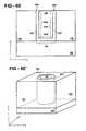
- FIG. 1Ais a cross sectional view of a memory device comprising conductive sidewall spacers as electrical contacts;
- FIG. 1Bis a three-dimensional view of the conductive sidewall spacers shown in FIG. 1A;
- FIG. 1Cis a cross-sectional view, parallel to the y-z plane, of a memory element using conductive sidewall spacers with rapier modification;
- FIG. 1Dis a three-dimensional view of conductive sidewall spacers with rapier modification
- FIGS. 2A-2Sshows a process for making the memory element of FIG. 1C
- FIG. 3Ais a three-dimensional view of a memory device having a cylindrically shaped conductive sidewall spacer as an electrical contact;
- FIG. 3Bis a three-dimensional view of cylindrically shaped conductive sidewall spacer with raised portions extending from the top edge of the sidewall spacer;
- FIG. 3Cis a side view of a memory element using the electrical contact from FIG. 3B;
- FIG. 4Ais a conductive liner formed in a trench
- FIG. 4Bis a conductive liner formed in a rectangular opening
- FIG. 4Cis a conductive liner formed in a circular opening
- FIG. 5Ais a three-dimensional view of a memory device using a conductive liner as an electrical contact
- FIG. 5Bis a cross-sectional view of the memory device of FIG. 5A;
- FIG. 5Cis a three-dimensional view of a cylindrically shaped conductive liner with raised portions extending from the top edge of the conductive liner;
- FIG. 5Dis a side view of a memory element incorporating the electrical contact from FIG. 5C;
- FIGS. 6 A- 6 S′is an embodiment of a process for making a memory element shown in FIG. 5D;
- FIG. 7is an example of a conductive liner with raised portions extending from a top edge of the liner's sidewall layers.
- FIG. 8is an example of an electrical contact having an increased resistivity in a region adjacent to the memory material.
- the present inventionis directed to programmable resistance memory elements.
- the memory elementcomprises a volume of memory material which is programmable between a first resistance state and a second resistance state in response to an electrical signal.
- the memory elementfurther comprises a means of delivering the electrical signal to the volume of memory material.
- the means of delivering the electrical signalcomprises a first and a second electrical contact, also referred to as first and second electrodes, which are in electrical communication with the volume of memory material.
- the electrical contacts or electrodesdo not have to be in physical contact with the memory material. (It is noted, that as used herein, the terminology “electrical contacts” and “electrodes” are synonymous and may be used interchangeably).
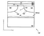
- FIG. 1Ais an cross-sectional view of a memory device 100 formed on a semiconductor substrate 102 .
- the cross-sectional viewis parallel to the x-z plane.
- the y-z planeis perpendicular to the plane of the illustration of FIG. 1 A.
- the memory device 100comprises two independent memory elements.
- the first memory elementcomprises a first electrical contact 130 A (a bottom electrode), a layer of memory material 290 and a second electrical contact 300 (a top electrode).
- the second memory elementcomprises a first electrical contact 130 B (a bottom electrode), a layer of memory material 290 and a second electrical contact 300 (a top electrode).
- the volume of memory materialis a substantially horizontally disposed layer of memory material 290 .
- the memory material 290 and the second electrical contact 300are shared by the first and second memory elements.
- each memory elementhas a separate volume (or layer) of memory material and a separate second electrical contact.
- Dielectric regions 140 and 128may be formed of silicon dioxide. Region 140 electrically isolates the bottom electrical contact 130 A from the bottom electrical contact 130 B.
- An upper dielectric region 180is deposited on top of the memory device 100 .
- the upper dielectric layer 180may comprise boron-phosphate silica glass (BPSG). Reference to the electrical contact 130 A,B refers to either electrical contact 130 A or electrical contact 130 B.
- BPSGboron-phosphate silica glass
- Each of the electrical contacts 130 A and 130 B shown in FIG. 1Ais a conductive layer. More specifically, each is a conductive sidewall layer in the form of a conductive sidewall spacer. A conductive sidewall layer may be formed by the substantial conformal deposition of a conductive material onto a sidewall surface. In FIG. 1A, sidewall surfaces 128 S and bottom surface 106 form a trench extending perpendicular to the plane of the illustration.
- each conductive spacer 130 A,Bis “edgewise adjacent” to the memory material. That is, only edge 132 or a portion of edge 132 of conductive spacer 130 A,B is adjacent to the memory material 290 . The remainder of the conductive spacer is remote to the memory material. Hence, substantially all electrical communication between the conductive spacer 130 A,B and the memory material 290 occurs through all or a portion of edge 132 . It is noted that edge 132 does not have to be in actually physical contact with the memory material. Also, in an alternate configuration it is possible to position the layer 290 of memory material so that it is adjacent to an edge of only one of the conductive spacers.
- FIG. 1Bis an idealized three-dimensional representation of conductive spacers 130 A,B showing their thickness “t”, width “w” and height “h”.
- the thickness “t” of the conductive sidewall spacer 130 A,Bis the lateral dimension of the spacer along the x-axis dimension in the x-z plane (parallel to plane of the illustration).
- the thickness “t” of conductive sidewall spacer 130 A,Bmay have a dimension which is smaller than what is producible by conventional photolithography.
- the width “w”is the lateral dimension of the conductive spacer along the y-axis in the y-z plane (perpendicular to the plane of the illustration of FIG. 1 A).
- the height “h”is the distance above the substrate 102 .
- the “area of contact”is the portion of the surface of an electrical contact through which the electrical contact electrically communicates with the memory material. While not wishing to be bound by theory it is believed that reducing the size of the area of contact reduces the volume of the memory material programmed, thereby reducing the total current needed to program the memory device.
- substantially all electrical communication between the memory material 290 and conductive sidewall spacer 130 A,Boccurs through all or a portion of edge 132 .
- the area of contact between the conductive spacer 130 A,B and the memory material 290is at least a portion of an edge the conductive sidewall spacer. The area of contact is thus very small and is proportional to the thickness of the conductive spacer adjacent to the memory material.
- each conductive sidewall spacer 130 A,Bhas a substantially uniform width “w” (dimension of the spacer along the y-axis).
- each conductive sidewall spacermay be formed so that its width is reduced (i.e., the conductive spacer is made narrower) adjacent to the memory material. Reducing the width “w” of the sidewall spacer adjacent the memory material reduces the area of contact between the conductive spacer and the memory material.
- This embodimentreferred to as a “rapier” design of the conductive spacer, is shown in FIG. 1 C.
- FIG. 1Cis a cross-sectional view of a memory device 100 ′ using a conductive sidewall spacer 130 ′A,B with a rapier design.
- the plane of the illustrationis parallel to the y-z plane.
- the top edge 132 of the conductive sidewall spacerhas been appropriately etched so that its width w is reduced adjacent to the memory material.
- each conductive spacerhas been appropriately recessed to form a protrusion or raised portion 135 adjacent to the memory material.
- the raised portion 135extends from the recessed edge 132 ′ and terminates at a distal end or top surface 137 adjacent the memory material 290 .
- the top surface 137 of the raised portion 135is also referred to as the “tip” or “peak” of the raised portion.
- 1Dis a idealized three-dimensional representation of the conductive spacers 130 ′A,B having raised portions 135 that extend from the edges 132 ′.
- the top surface or tip 137 of each of the raised portionshas a thickness “t” and a width “w2”.
- the thickness “t”is the thickness of the conductive layer 130 ′A,B adjacent to the memory material (not shown).
- thickness “t”is less than about 750 Angstroms, more preferably less than about 500 Angstroms and most preferably less than about 300 Angstroms.
- the width “w2” of the raised portion 135 adjacent the memory materialis less than the width “w1” of the sidewall layer 130 ′A,B adjacent the substrate 102 .
- the width “w2”is less than 700 Angstroms, more preferably less than 600 Angstroms and most preferably less than about 500 Angstroms.
- the thickness “t”, the width “w2” as well as the surface area of the tip 137may all be made smaller than what is permitted by photolithographic techniques.
- the dimensions of the top surface 137are sufficient so that the area of contact between the raised portion 135 and the memory material is preferably less than about 0.005 micron 2 , more preferably less than about 0.0025 micron 2 , and most preferably less than about 0.0015 micron 2 .
- the raised portion 135may be made to have substantially vertical sidewalls (for example, substantially uniform width “w2” and substantially uniform thickness “t”), or it may be made to taper as it extends toward the tip 137 (for example, by tapering the width “w2 and/or by tapering the thickness “t”).
- the shape of the raised portion 137is not limited to any particular shape. Examples of possible shapes include conical, pyramidal, prismatic and wedge-shaped frustums.
- the top surface or tip 137 of the raised portion 135may be substantially flat or rounded. It is also conceivable that the distal end or tip 137 may also be sharpened.
- the height of the raised portion 135 as well as the extent of any taperingmay be controlled.
- a dielectric material 145is preferably positioned between the conductive sidewall layer 130 ′A,B and the memory material so that only the top surface 137 is exposed and in electrical contact with the memory material. Hence, substantially all electrical communication between each conductive layer 130 ′A,B and the memory material occurs through at least a portion of the top surface or tip 137 of the raised portion 135 .
- the area of contact between each bottom electrode 130 ′A,B and the memory materialis thus preferably defined by the top surface or tip 137 .
- the area of contacthas an area less than about 0.005 micron 2 , more preferably less than about 0.0025 micron 2 , and most preferably less than about 0.0015 micron 2 .
- the raised portion 135be made to protrude into the memory material so that more of the surface of the raised portion 135 is in electrical contact with the memory material. It is noted that more than one raised portion may be formed on the edge 132 ′ of each conductive layer 130 ′A,B.
- the raised portions 135may be made by forming a sidewall spacer over the conductive sidewall layers 130 A,B that are shown in FIG. 1 B. Specifically, the spacer is positioned above the conductive sidewall layers 130 A,B where it is desired to position the raised portions 135 .
- the spacerserves as a mask for either an anisotropic or isotropic etch. That is, the exposed sections of the edges 132 of the sidewall layers will be etched away and recessed while the section underlying the mask is at last partially protected from the etch so as to form raised portions or protrusions that extend from the recessed edges.
- the spacer which is used as the maskis not limited to any particular material.
- the masking spaceris formed of a dielectric material such as an oxide or a nitride material.
- the masking spacermay also be formed of a semiconductor material such as a polysilicon.
- the spacermay be formed in many different ways.
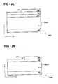
- FIGS. 2A-2SAn embodiment of a method for fabricating the memory device 100 ′ of FIG. 1C is shown in FIGS. 2A-2S.
- a substrate 102is provided and a dielectric layer 128 is deposited on top of the substrate 102 to form the structure 200 A shown in FIG. 2 A.
- the dielectric layer 128may be a dielectric material such as silicon dioxide SiO 2 which may be deposited by means such as chemical vapor deposition (CVD).
- the dielectric layer 128is then appropriately masked and etched to form a window or opening in the dielectric layer 128 .
- the openingpreferably exposes a portion of the substrate (and preferably the exposed portion of the substrate is a conductive portion of the substrate).
- the openingis a trench 170 which runs perpendicular to the plane of the illustration.
- the trench 170has sidewall surfaces 128 S (corresponding to the sidewall surfaces of the dielectric regions 128 ) and bottom surface 106 .
- a layer 133 of a conductive materialis deposited onto the structure 200 B to form the structure 200 C shown in FIG. 2 C.
- the depositionis a substantially conformal deposition.
- the layer 133is deposited onto the top surfaces 128 T of the dielectric regions 128 , onto the sidewall surfaces 128 S of the dielectric regions 128 , and onto the bottom surface 106 of the trench 170 .
- portions of the layer 133are deposited along the two sidewall surfaces 128 S of the trench 170 .
- These portions of the layer 133are sidewall layer portions 133 S of the layer 133 .
- the conformal deposition of layer 133may be done using chemical vapor deposition techniques. Other possible deposition methods may be used as long as the sidewall surfaces 128 S are appropriately covered by the layer 133 .
- the material 133may be any conductive material.
- itmay be a metal, a metal alloy or a doped polysilicon.
- materials which may be used for layer 133are include, but are not limited to, n-type doped polysilicon, p-type doped polysilicon, p-type doped silicon carbon alloys and/or compounds, n-type doped silicon carbon alloys and/or compounds, titanium-tungstem, tungsten, tungsten silicide, molybdenum, and titanium nitride.
- Other examplesinclude titanium carbon-nitride, titanium aluminum-nitride, titanium silicon-nitride, and carbon.
- the n-type polysiliconmay be formed “in situ” by depositing polysilicon in the trench 170 using a CVD process in the presence of phosphene. Alternately, the n-type polysilicon may be formed by first depositing polysilicon and then doping the polysilicon with phosphorous or arsenic. P-type doped polysilicon may be formed by first depositing polysilicon and then doping the polysilicon with boron.
- the thickness of layer 133is between about 50 and about 1000 Angstroms, and more preferably between about 100 and about 500 Angstroms.
- the layer 133is conformally deposited it is then anisotropically etched.
- the anisotropic etchremoves those sections of the layer 133 which are substantially horizontally disposed and leaves those sections which are substantially vertically disposed. Specifically, the anisotropic etch removes the substantially horizontally disposed sections of the layer 133 that were deposited on top surfaces 128 T of the regions 128 . It also removes the substantially horizontally disposed section of the layer 133 deposited onto the bottom surface 106 of trench 170 .
- the anisotropic etchleaves those sections of the layer 133 conformally deposited along the sidewall surfaces 128 S. Hence, the anisotropic etch leaves the sidewall layer portions 133 S of the layer 133 .
- the results of the anisotropic etchare shown as structure 200 D in FIG. 2 D.
- the sidewall layer portions 133 S of layer 133form the conductive sidewall spacers 130 A,B.
- the sidewall spacers 130 A,Bare formed having the top edges 132 .
- the conductive sidewall spacers 130 A,B shown in FIG. 2Dextend continuously along the y-axis dimension of the trench 170 (that is, perpendicular to the plane of the illustration of FIG. 2 D).
- the next step in the processis to mask and etch the conductive sidewall spacers 130 A,B so as to form a plurality of individual conductive sidewall spacers along the y-axis dimension of the memory array. These conductive spacers define individual memory elements along the y-axis dimension of the memory array.
- the dielectric materialsuch as silicon dioxide is then deposited into the opening 170 and onto the sidewall spacers 130 A,B.
- the dielectric materialpreferably fills the opening 170 .
- the dielectric material 140is preferably deposited into the trench 170 and on top of the dielectric layers 128 of structure 200 D to form structure 200 E.
- the depositionmay be done using a chemical vapor deposition process.
- the structure 200 Emay then chemically mechanically polished (CMP) or dry etched to form the structure 200 F shown in FIG. 2 F.
- CMPchemically mechanically polished
- the chemical mechanical polishing or dry etchingpreferably planarizes the top surfaces of the sidewall layers 130 A,B to expose at least a portion of one or both of the top edges 132 . In the embodiment shown in FIG. 2F, at least a portion of each of the edges 132 is exposed.
- a three dimensional representation of the structure 200 Fis shown in FIG. 2 F′.
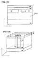
- a first oxide layer 240(for example, silicon dioxide from a TEOS source) is deposited onto the top surface of structure 200 F to form the structure 200 G shown in the three-dimensional representation of FIG. 2 G.
- FIG. 2 G′is a cross-sectional view of the same structure 200 G parallel to the y-z plane and parallel to the width “w” of the sidewall spacer 130 A,B.
- the dimension of the first oxide layer 240is between about 200 Angstroms and 500 Angstroms, and more preferably about 300 Angstroms.
- the first oxide layer 240may be deposited using a chemical vapor deposition process.
- a layer 250 of polysiliconis then deposited on top of the oxide layer 240 to form structure 200 H shown in the cross-sectional FIG. 2H (parallel to the y-z plane) and in the three-dimensional representation of FIG. 2 H′.
- the dimension of layer 250is approximately 1000 Angstroms.
- the structure 200 His then appropriately masked and etch.
- a layer of photoresist materialis applied on top of the layer of polysilicon 250 .
- the layer of photoresistis appropriately patterned (i.e., a pattern on a mask is transferred to the layer of photoresist) and a portion of the photoresist layer is removed to form the photoresist mask 260 shown in the three-dimensional view of FIG. 2I.
- a top view of the structure 200 I parallel to the x-y planeis shown in FIG. 2 I′.
- FIG. 2 I′shows the relative positioning of the photoresist mask 260 relative to the top edges 132 of the conductive spacers 130 A,B.
- a cross-sectional view of structure 200 I, parallel to the y-z plan,is shown in FIG. 2 I′′.
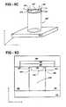
- the structure 200 Iis then preferably dry etched to remove the portion of the polysilicon layer 250 which is not protected by the photoresist mask 260 , thereby forming the structure 200 J shown in FIG. 2 J.
- the etch usedis selective to the oxide layer 240 .
- the etchforms a sidewall surface 252 in the polysilicon layer 250 .
- the photoresist 260is then stripped from structure 200 J to form structure 200 K shown in FIG. 2 K.
- a second oxide layer 270(such as silicon dioxide) is then deposited onto the structure 200 K to form the structure 200 L shown in FIG. 2 L.
- the layer 270is deposited to a thickness of about 600 Angstroms.
- the second oxide layer 270is deposited onto top horizontal surface of the polysilicon layer 250 as well as onto the exposed portion of the first oxide layer 240 . It is also deposited along the sidewall surface 252 of the polysilicon layer 250 .
- the oxide layer 270is then anisotropically etched to remove the horizontally disposed portions of second oxide layer 270 and leave the vertically disposed portion 270 A along the sidewall surface 252 .
- the resulting structureis shown as structure 200 M in FIG. 2 M.
- the remaining portion the oxide layer 270is the portion 270 A.
- the portion 270 Ais a sidewall spacer.
- the remaining portion of the polysilicon layer 250 shown in FIG. 200Mis then removed. This is preferably done by using a polysilicon dry etch. It is possible to use a wet polysilicon etch as well.
- the resulting structureis shown as structure 200 N in FIG. 2 N.
- the structure 200 Nis subjected to an anisotropic etch to remove the portions of the first oxide layer 240 that are not covered by the spacer 270 A, leaving the oxide spacer 270 B as shown by structure 200 O in FIG. 2O.
- a three dimensional representation of the structure 200 Ois shown in FIG. 2 O′.
- FIG. 2 O′′A top view (parallel to the x-y plane) of the oxide spacer 270 B and its positioning relative to the top surfaces 132 of the conductive layers 130 A,B is shown in FIG. 2 O′′.
- the spacer 270 Boverlies a portion of each of the exposed edges 132 of the sidewall spacers 130 A,B.
- the “thickness” of the oxide spacer 270 Bi.e. the spacer's lateral dimension in the y-axis dimension
- the thickness dimension of the oxide spacer 270 Bis preferably less 1000 Angstroms.
- the thickness of the oxide spaceris preferably less than 700 Angstroms, more preferably less than 600 Angstroms and most preferably less than about 500 Angstroms.
- FIG. 2Pis a cross-section view through a recessed conductive layer 130 ′A,B parallel to the y-z plane.
- the etch usedmay, for example, be a wet etch or a dry etch.
- the etch usedis a dry etch such as a plasma etch.
- the etchis preferably anisotropic so as to form raised portions 135 having substantially straight sidewalls.
- an isotropic etchmay be used which removes a portion of the conductive material underneath the spacer and forms raised portions with sloped or tapered sidewalls.
- the raised portions 135may be tapered (where the degree of tapering is controlled by the etching process used).
- the raised portions 135may have a height of about 500 Angstroms to about 2500 angstroms.
- a layer 145 of a dielectric material(such as silicon dioxide) is then deposited onto the top of the structure 200 P preferably by using conventional deposition methods (such as chemical vapor deposition) to form the structure 200 Q shown in FIG. 2 Q.
- the materialis deposited into the recesses 138 , onto the recessed edges and at least partially over the raised portions.
- the dielectric layer 145 and the oxide spacer 270 Bmay then be chemically mechanically polished (CMP) to expose at least a portion of the top surface or tip 137 of each of the raised portions 135 and form the structure 200 R shown in FIG. 2 R. (Of course, it may be possible to expose at least a portion of just one of the tips 137 ).
- a layer of memory material 290 and a second electrical contact 300i.e., a top electrode
- a barrier layermay, optionally, be formed on top of the structure 200 R.
- the barrier materialwould be formed between the tip (or top surface) 137 of the raised portion and the memory material.
- Barrier layer materialsmay be chosen to increase the conductivity between the electrical contact and the memory material, and/or improve the adhesion between the electrical contact and the memory material, and/or to prevent the electromigration of the electrical contact material into the memory material. Examples of certain barrier layer materials include, but are not limited to, titanium silicide, cobalt silicide and tungsten silicide.
- etching the conductive sidewall layersforms the narrow recesses 138 where the conductive layers are not underlying the oxide spacer 270 B.
- the raised portions 135may be made with the use of oxide spacers. As noted above, other materials may be used to form the spacers. In another embodiment of the present invention, the raised portions may be also made with nitride spacers that are preferably formed from silicon nitride. Referring FIGS. 2G through 2L, nitride spacers may be formed by replacing the first oxide layer 240 with a first silicon nitride layer, by replacing the polysilicon layer 250 with an oxide layer (such as silicon dioxide from a TEOS source) and by replacing the second oxide layer 270 with a second silicon nitride layer. The polysilicon etch (used to etch the polysilicon 250 as shown in FIGS.
- the disclosed technique for forming raised portions above a conductive materialshould not be limited to the embodiments disclosed herein.
- the spacersmay be formed using many different techniques.
- the spacersmay be formed from many different materials including dielectrics (for example, oxide and nitride), semiconductor materials (such as polysilicon) and conductors (such as aluminum).
- dielectricsfor example, oxide and nitride
- semiconductor materialssuch as polysilicon
- conductorssuch as aluminum
- the materials chosen for the layers 240 , 250 , 260 and 270are not limited to the embodiments provided and a wide range of materials may be used for each of the layers.
- the particular materials selected for each of the layersare preferably chosen to provide the proper selectivity during the various etching processes as will be recognized by persons of ordinary skill in the art.
- the raised portions or protrusions as well the remaining conductive layermay be formed from any conductive material.
- materialsinclude, but are not limited to, n-type doped polysilicon, p-type doped polysilicon, p-type doped silicon carbon alloys and/or compounds, n-type doped silicon carbon alloys and/or compounds, titanium-tungstem, tungsten, tungsten silicide, molybdenum, and titanium nitride.
- Other examplesinclude titanium carbon-nitride, titanium aluminum-nitride, titanium silicon-nitride, and carbon.
- the raised portion 135extends from an edge of conductive layer 130 ′A,B.
- the conductive layeris a substantially planer, sidewall layer formed along the sidewall surface of a trench by depositing a layer of conductive material into the trench and then anisotropically etching the layer to remove the horizontally disposed surfaces.
- raised portionsmay be formed on any conductive material having any physical geometry.
- raised portions or protrusionsmay be formed on an edge of any conductive layer (such as an conductive sidewall) having any physical geometry.
- Alternate forms of conductive sidewall layersmay be made by the conformal deposition of a conductive material onto sidewall surfaces having various shapes and configurations.
- a layer of conductive materialmay be substantially conformally deposited onto the sidewall surfaces of an opening (such as a via), a mesa or a pillar.
- the opening, mesa or pillarmay be round, square, rectangular or irregularly shaped (likewise, the opening may be a trench).
- Anisotropically etching the conformally deposited conductive layerremoves the horizontally disposed portions of the deposited layer and leaves only one or more vertically disposed portions.
- the remaining one or more vertically disposed portionsare sidewall layers in the form of conductive sidewall spacers having different shapes.
- the sidewall spacer formed, for example, by the conformal deposition of a conductive material into a circular opening (followed by an anisotropic etch)will be a conductive sidewall layer in the form of a cylindrical surface having two open ends. The top edge of the layer will be in form of an annulus.
- Changing the shape of opening (or pillar or mesa)will change the shape of the sidewall spacer. That is, the lateral cross section of the conductive sidewall spacer (i.e. the cross section parallel to the substrate) corresponds to the shape of the opening, mesa or pillar. Alternately, it may be rectangular or irregularly shaped.
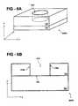
- FIG. 3Ashows a three-dimensional view of a cylindrical, conductive sidewall spacer 330 formed in a circular opening (and thus having a horizontal cross-section in the shape of an annulus).
- the cylindrical conductive spacer 330comprises a single, cylindrically shaped sidewall layer.
- the thickness “t” of this cylindrically shaped sidewall layeris the distance between the inner and outer cylindrical surfaces as shown in FIG. 3 A.
- the cylindrical sidewall layerhas two open ends or “rims” forming the top edge 332 and the bottom edge 331 .
- the top and bottom edges 332 and 331 of the cylindrically shaped conductive sidewall layer 330are annular surfaces formed by intersecting the conductive layer 330 with planes substantially parallel to the substrate. In the embodiment shown in FIG.
- the layer of memory material 290is adjacent only to the top end (i.e., the top edge 332 ) of the cylindrical sidewall spacer 330 . Substantially all electrical communication between the conductive spacer 330 and the memory material 290 is through the top edge 332 or a portion of the top edge 332 . Hence, the area of contact between the conductive spacer 330 and the memory material 250 is the edge 332 or a portion of the edge 332 . (That is, all or a portion of the annular surface 332 ).
- FIG. 3Bis a three-dimensional representation of a cylindrical conductive sidewall layer 330 ′ that includes raised portion or protrusions 335 that extend from the edge 332 ′. Each raised portion 335 extends from edge 332 ′ to an end or tip 337 adjacent the memory material (not shown). As noted above, the raised portions 335 are not limited to any particular shape. In the embodiment shown, the raised portions 335 have a thickness “t” (proportional to the thickness of the conductive layer) and a width “w”.
- Conductive layer 330 ′is in the form of a cylindrical conductive spacer.
- the raised portionsmay be formed on the top edge of the cylindrical conductive layer 330 ′ with the use of oxide spacers or nitride spacers as described above. An example of forming the raised portions atop the annular edge of a cylindrical sidewall layer will be given below.
- substantially all electrical communication between the conductive spacer 330 ′ and the memory materialis through one or more of the raised portions 335 . More preferably, substantially all electrical communication between the conductive spacer 330 ′ and the memory material is through the upper surface or tip 337 of one or more of the raised portions 335 .
- the electrical contact 330 ′ and memory materialmay be positioned so that only all or a portion of the top end or tip 337 of one or more of the raised portions 335 are adjacent to the memory material while substantially all of the remaining portion of the electrical contact is remote to the memory material.
- FIG. 3Cis a two dimensional side view of the cylindrical conductive layer 330 ′, parallel to the x-z plane, showing the memory material 290 as well as the top electrical contact 300 (and also insulation materials 128 , 140 and 180 ).
- both of the raised portions 335are in electrical communication with the memory material.
- the memory material and the raised portions 335 and the memory materialbe positioned relative to each other so that only one of the protrusions 335 is touching the memory material.
- only the top surfaces or tips 337are adjacent the memory material while the remainder of the electrical contact is remote to the memory material.
- the conductive sidewall layershave been formed as conductive sidewall spacers.
- a conductive sidewall layermay be formed as a portion of a “conductive liner”.
- the conductive lineris preferably a single layer of conductive material deposited on the sidewall surfaces as well as the bottom surface of a trench, opening (such as a via), or the like. Examples of conductive liners are shown in FIGS. 4A-C.
- FIG. 4Athe conductive liner 430 A is formed in a trench.
- FIG. 4Bis an example of a conductive liner 430 B formed in a rectangular opening.
- each conductive linerhas one or more sidewall layer portions as well as a bottom layer portion.
- the top end of the conductive linersis an open end having a top edge 432 .
- the “top edge” 432 of each conductive lineris the surface formed by intersecting the respective conductive liner with a plane substantially parallel with the substrate 102 ). It is noted that the U-shaped conductive liner shown in FIG. 4A has a “dual” top edge 432 .
- the sidewall layer portionsare substantially vertically disposed. However, this does not have to be the case.
- the sidewall layer portionsmay be tilted. This would be the case if the conductive liners were formed in either a trench or via having angled sidewall surfaces.
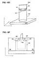
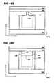
- FIGS. 5A and 5Bdepict an embodiment of the memory element where the bottom electrical contact is a conductive liner 630 formed in a circular opening.
- FIG. 5Ais a three-dimensional view of the memory element while FIG. 5B is a cross-sectional view parallel to the x-z plane.
- the conductive liner 630is a cylindrical shell having an open top end (remote to and facing away from the substrate 102 ) and a closed bottom end (preferably adjacent to and in electrical communication with the substrate).
- the open top endhas an annular top edge 632 .
- the conductive liner 630comprises a cylindrically shaped sidewall layer portion 630 S and a bottom layer portion 630 B.
- the conductive liner 630is in the shape of a cylindrically shaped cup. As shown in FIG. 5B, the sidewall layer portion 630 S forms the side of the cup while the bottom layer portion 630 B forms the bottom of the cup.
- the top edge 632may be referred to as the “rim” of the cup.
- the conductive linermay have other cup shapes such as a paraboloid, hemisphere, cone, and frustum.
- the layer 290 of memory materialis preferably a planar, substantially horizontally disposed layer positioned adjacent to the open end (i.e., top edge 632 ) of the conductive liner 630 .
- the memory materialis adjacent only to the top edge 632 (i.e., the rim) of the conductive liner 630 or a portion of the top edge 532 of the conductive liner.
- the remainder of the conductive liner 630is remote to the memory material.
- substantially all electrical communication between the conductive liner 630 and the memory materialoccurs through the edge 532 or a portion of the edge 632 .
- the area of contactis defined by all or a portion of the edge 632 .
- the edge 632is an annulus having a thickness equal to the thickness of the conductive liner 630 .
- the thickness of this annulus, and hence the area of contact between the conductive liner and the memory materialmay be reduced by decreasing the thickness of the conductive liner 630 deposited into the circular via. It is noted that it is possible that one or more intermediate layers be disposed between the memory material and the conductive liner.
- FIG. 5Cshows the cylindrical conductive liner 630 ′ disposed on top of a substrate 102 .
- the conductive liner 630 ′includes at least one raised portion or protrusion 635 .
- Each of the raised portionsextends from the top edge 632 ′ to a distal end or tip 637 (also referred to as a top surface) adjacent the memory material (the memory material is not shown in this diagram).
- the raised portions 635each have a thickness “t” (which is substantially the same as the thickness of the remainder of the conductive liner 630 ′) and a width “w”.
- substantially all electrical communication between the conductive sidewall spacer 630 ′ and the memory materialis through one or more of the raised portions 635 . More preferably, substantially all electrical communication between the conductive spacer 630 ′ and the memory material occurs through the top surface or tip 635 of one or more of the raised portions 635 .
- the electrical contact 630 ′ and memory materialmay be positioned so that only the top surface 637 of one or more of the raised portions 635 is adjacent to the memory material while substantially all of the remaining portion of the electrical contact is remote to the memory material.
- FIG. 5Dshows a side view of a memory element, parallel to the x-z plane, made using the conductive liner 630 ′. Shown are memory material 290 and second electrical contact 300 . In FIG. 5D, the tips 637 of both protrusions 635 are in electrical contact with the memory material; however, it is possible that the memory material be positioned so that it is in electrical contact with only the upper surface 637 of only one of the protrusions 635 . The base of the conductive liner 630 ′ is adjacent to and in electrical communication with the substrate 102 .
- the raised portions 635may be formed with the use of sidewall spacers as described above.
- the sidewall spacersmay be formed, for example, of oxide or silicon nitride.
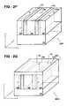
- An embodiment of a method for fabricating the conductive liner 630 ′is shown FIGS. 6 A- 6 S′. Referring first to FIG. 6A, a substrate 102 is provided and a dielectric layer 128 is deposited on top of the substrate 102 .
- the dielectric layermay be formed from silicon dioxide and may be deposited by a chemical vapor deposition process.
- the dielectric layer 128is then appropriately masked and etched to form a window or opening in the form of opening 610 in the dielectric 128 as shown.
- the openingmay be round, square, rectangular or irregularly shaped.
- the dielectric layer 128may be masked and etched to form a trench.
- the opening(or trench) is made through the dielectric layer 128 to the substrate 102 .
- the resulting structure 600 Ais a circular opening 610 which is formed in the dielectric 128 .
- FIG. 6Bis a cross-sectional view (parallel to the y-z plane) of the three-dimensional structure 600 A shown in FIG. 6 A.
- the sidewall surface 128 S and the bottom surface 106 of the circular opening 610is shown in FIG. 6 B.
- the openingexposes at least a portion of the substrate.
- a layer 633 of a conductive materialis deposited on top of the structure shown in FIGS. 6A and 6B to form the structure 600 C shown in FIG. 6 C.
- the layer 633 of conductive materialis conformally deposited on top surfaces 128 T of the dielectric region 128 , on the sidewall surface 128 S of the region 128 and the bottom surface 106 of the opening 640 .
- the layer 633has a top portion 633 T, a sidewall layer portion 633 S, and a bottom layer portion 633 B.
- a layer of dielectric material 140(such as silicon dioxide) may then be deposited on top of the layer 633 so as to preferably fill the opening 610 and form the structure 600 D shown in FIG. 6 D.
- the structure 600 Dmay then be chemically mechanically polished (CMP) or dry etched so as to planarize the top surface thereby removing a portion of layer 140 as well as the top layer portion 633 T of the layer 633 .
- CMPchemically mechanically polished
- the etchforms a cylindrical, cup-shaped conductive liner 630 having a sidewall layer portion 630 S along the sidewall 128 S and a bottom layer portion 630 B along the bottom surface 106 as shown in FIG. 6 E.
- the etchalso forms the edge 632 .
- the edge 632has the shape of an annulus.
- the planarization stepforms an edge which is substantially planar.
- Figure E′shows a three-dimensional representation of the structure 600 E from FIG. 6 E.
- One or more raised portions or protrusionsmay be formed atop the edge 632 .
- the processing steps for forming raised portions that extend from the top edge of the conductive linerare the similar to those described above with respect to the conductive sidewall spacers.
- a first oxide layer 640is deposited on top of the conductive liner 600 E to form the structure 600 F shown in the three-dimensional representation of FIG. 6 F and in the cross-sectional view (parallel to the y-z plane) of FIG. 6 F′.
- a polysilicon layer 650is deposited onto the first oxide layer 640 so form structure 600 G as shown in FIGS. 6 G and 6 G′.
- a photoresist resist layeris deposited onto the polysilicon layer 650 and appropriately patterned to form photoresist mask 660 as shown in FIG. 6H.
- a top view (parallel to the x-y plane) of the positioning of the photoresist layer 660 relative to the annular edge of the conductive cup 630is shown in FIG. 6 H′.
- a cross-sectional view (parallel to the y-z plane)is shown in FIG. 6 H′′.
- the polysilicon layer 650is appropriately patterned and etched to form a sidewall surface 652 in the layer 650 as shown in structure 600 I of FIG. 6 I.
- the photoresist materialis then removed as shown in FIG. 6J.
- a second oxide layer 670is conformally deposited over the top surface and the sidewall surface 652 of the remaining portion of the polysilicon layer 650 as well as over the top surface of the first oxide layer 640 as shown in FIG. 6 K.
- the horizontally disposed portions of the second oxide layer 670are then removed preferably by an anisotropic etch of the oxide layer 670 leaving the vertically disposed oxide portion 670 A along the sidewall surface of the polysilicon layer 650 as shown in FIG. 6 L.
- the remaining portion of the polysilicon layer 650is then removed as shown in FIG. 6 M.
- the remaining oxide layer 640 and oxide portion 6 Aare then anisotropically etched to remove that portion of the oxide layer 640 that is not covered by the oxide spacer 670 A.
- FIG. 6 N′′is a top view parallel to the x-y plane of the structure 600 N. As shown in FIG. 6 N′′, the oxide spacer 670 B is overlying a portion of the edge 632 .
- the conductive layer 630is then etched to form one or more raised portions underneath the spacer.
- the conductive layer not covered by the spaceris etched away and removed to form a recessed edge 632 ′.
- at least a portion of the conductive layer covered by the oxide spacer 670 Bis at least partially protected from the etch to form the raised portions 635 that extend upwardly from the recessed edge.
- a side view (parallel to the y-z plane) of an etched conductive cup 630 ′ having recessed edge 632 ′ and raised portions 635is shown in FIG. 6 P.
- Recession 638is the gap formed between the oxide materials 128 , 140 as a result of etching the conductive liner 630 .
- the etchmay be anisotropic or isotropic.
- the etchmay be a dry etch or a wet etch.
- An oxide layer 680is then deposited into the recession 638 and on top of dielectric layers 128 and 140 as shown (as a cross-sectional view parallel to the y-z plane) in FIG. 6 Q.
- the oxide layer 680 and the oxide spacer 670 Bmay then be chemically mechanically polished to expose at least a portion of the top surfaces or tips 637 of the raised portions 635 and to form structure 600 R as shown in FIG. 6R.
- a layer of programmable resistance memory materialis disposed adjacent at least a portion of the raised portions. Referring to FIG. 6S, a layer of memory material 690 is deposited on top of the structure 600 R and, in particular, over at least a portion of one or both of the tips 627 .
- FIG. 6 S′shows an alternate side view of the structure 600 S parallel to the x-z plane that shows the conductive liner 630 ′ and both of the raised portions 635 with tips 637 adjacent the memory material 690 . Only the top surfaces 637 of the raised portions 635 are adjacent to the memory material 690 while the remainder of the raised portions as well as the remainder of the conductive liner 630 ′ is remote to the memory material 690 . It is noted that the memory layer 690 may be positioned to that it is adjacent to only one of the raised portions 635 .
- the oxide layer 680 shown in FIG. 6Qit is possible to etch the dielectric regions 128 and 140 (shown in FIG. 6P) to the level of the recessed edge 632 ′. This avoids the need to have the oxide material 680 fill the narrow gap 638 and also facilitates the chemical mechanical polishing. Also, as discussed above, it is possible to form protrusions 635 by using spacers formed from other dielectrics such as silicon nitride. Moreover, it is also possible to form spacers from semiconductor materials such as polysilicon or from conductors such as aluminum.
- a sidewall spaceris used as a mask and a portion of the conductive material that does not underlie the mask (the sidewall spacer) is removed to form the raised portion.
- the sidewall spacermay be used which are not sidewall spacers.
- different types of patterned layersmay be used as masks to form the raised portions.
- the patterned layersmay simply be a portion of a layer (such as an oxide, nitride or polysilicon layer) which is formed on a portion of the edge of the conductive layer.
- the maskbe a thin vertically disposed strip which is not formed as a sidewall layer.
- a lateral dimension of the maskis a dimension of the mask as measured parallel to the substrate.
- a lateral dimensionmay, for example, be the dimension of the mask as measured along either the x-axis or the y-axis when the substrate is parallel to the x-y plane.
- at least one of the lateral dimensions of the maskis less than that which could be achieved through photolithography (i.e., it is less than a photolithographic limit).
- at least one of the lateral dimensionsis preferably less than about 1000 Angstroms.
- at least one of the lateral dimensionsis less than about 700 Angstroms, more preferably less than about 600 Angstroms, and most preferably less than about 500 Angstroms.
- a layer of polysilicon(a first layer) is deposited over the conductive material.
- the layer of polysiliconis then be patterned and etched to form a sidewall surface.
- An oxide layer(a second layer) is then deposited onto the sidewall surface of the polysilicon.
- the oxide layeris anisotropically etched to remove the horizontally disposed surfaces and leave the sidewall spacer on the polysilicon.
- the polysiliconis then removed to leave only the oxide sidewall spacer that can now be used as mask.
- a portion of the conductive material not covered by the spaceris etched so as to form a raised portion extending from the conductive material under the spacer.
- the polysilicon and the oxidemay, of course, be replaced with other materials.
- the materials chosen for the different layersdepend upon the underlying conductive material and also upon the appropriate selectivity during the various etching processes. Still other methods known in the art may be used to form the masking spacers.
- the raised portions or protrusionsmay be formed on an edge of the sidewall layers of different conductive liners. For example, they may be formed on the conductive liners shown in FIGS. 4A-4C.
- FIG. 7provides an example of a U-shaped conductive liner 720 that is formed in a trench.
- FIG. 7shows conductive liner 720 having two sidewall layer portions 730 and a bottom layer portion 740 .
- the raised portions or protrusions 735are formed on the edges 732 of the two sidewall layer portions 730 of the conductive liner 720 .
- the protrusions 735extend from the edges 732 to tips 737 .
- Substantially all of the electrical communication between the conductive liner 720 and the memory materialis preferably through one or both of the raised portions 735 , and more preferably, through one or both of the top surfaces 737 .
- raised portions or protrusionsmay be formed on an edge of a conductive sidewall layer to form novel electrical contact structures. More generally, raised portions may be formed on the edge of any conductive layer having any shape or orientation. Still, more generally, one or more raised portions may be formed on any conductive material having any physical geometry.
- the electrical contactsdeliver electrical current to the memory material.
- the electrical currentpasses through the electrical contacts and through the memory material, at least a portion of the electric potential energy of the electrons is transferred to the surrounding material as heat. That is, the electrical energy is converted to heat energy via Joule heating.
- the amount of electrical energy converted to heat energyincreases with the resistivity of the electrical contact (and memory material) as well as with the current density passing through the electrical contact and the memory material.
- FIG. 8shows the conductive layer 130 ′A,B from FIG. 1C where the protrusion 135 has a region R 2 (adjacent the memory material) which has a higher resistivity than the region R 1 remote to the memory material.
- U.S. patent application Ser. No. 09/620,318describes methods of making electrodes have two or more regions with different resistivities. The complete disclosure of U.S. patent application Ser. No. 09/620,318 is hereby incorporated by reference herein.
- the memory elements of the present inventionmay be electrically coupled to isolation/selection devices and to addressing lines in order to form a memory array.
- the isolation/addressing devicespermit each discrete memory cell to be read and written to without interfering with information stored in adjacent or remote memory cells of the array.
- the present inventionis not limited to the use of any specific type of isolation/addressing device.
- isolation/addressing devicesinclude field-effect transistors, bipolar junction transistors, and diodes.
- Examples of field-effect transistorsinclude JFET and MOSFET.
- Examples of MOSFETinclude NMOS transistors and PMOS transistors. Furthermore NMOS and PMOS may even be formed on the same chip for CMOS technologies.
- isolation/addressing devicewhich serves as an isolation/addressing device for that memory element thereby enabling that cell to be read and written without interfering with information stored in other adjacent or remote memory elements of the array.
- the memory element of the present inventioncomprises a volume of memory material.
- the volume of memory materialis a programmable resistance memory material which is programmable to at least a first resistance state and a second resistance state.
- the memory materialis preferably programmed in response to electrical signals.
- the electrical signals used to program the materialsare electrical currents which are directed to the memory material.
- the memory materialis programmable to two a resistance states so that each of the memory elements is capable of storing a single bit of information. In another embodiment, the memory material is programmable to at least three resistance states so that each of the memory elements is capable of storing more than one bit of information. In yet another embodiment, the memory material is programmable to at least four resistance states so that each of the memory elements is capable of storing at least two bits of information.
- the memory materialsmay have a range of resistance values providing for the gray scale storage of multiple bits of information.
- the memory materialsmay be directly overwritable so that they can be programmed from any of their resistance states to any other of their resistance states without first having to be set to a starting state.
- the same programming pulse or pulsesmay be used to program the memory material to a specific resistance state regardless of its previous resistance state.
- the same current pulse or pulsesmay be used to program the material to its high resistance state regardless of its previous state.
- the memory materialmay be a phase change material.
- the phase-change materialsmay be any phase change memory material known in the art.
- the phase change materialsare capable of exhibiting a first order phase transition. Examples of materials are described in U.S. Pat. Nos. 5,166,758, 5,296,716, 5,414,271, 5,359,205, 5,341,328, 5,536,947, 5,534,712, 5,687,112, and 5,825,046 the disclosures of which are all incorporated by reference herein.
- the phase change materialsmay be formed from a plurality of atomic elements.
- the memory materialincludes at least one chalcogen element.
- the chalcogen elementmay be chosen from the group consisting of Te, Se, and mixtures or alloys thereof.
- the memory materialmay further include at least one element selected from the group consisting of Ge, Sb, Bi, Pb, Sn, As, S, Si, P, O, and mixtures or alloys thereof.
- the memory materialcomprises the elements Te, Ge and Sb.
- the memory materialconsists essentially of Te, Ge and Sb.
- An example of a memory material which may be usedis Te 2 Ge 2 Sb 5 .
- the memory materialmay include at least one transition metal element.
- transition metalas used herein includes elements 21 to 30 , 39 to 48 , 57 and 72 to 80 .
- the one or more transition metal elementsare selected from the group consisting of Cr, Fe, Ni, Nb, Pd, Pt and mixtures or alloys thereof.
- the memory materials which include transition metalsmay be elementally modified forms of the memory materials in the Te—Ge—Sb ternary system. This elemental modification may be achieved by the incorporation of transition metals into the basic Te—Ge—Sb ternary system, with or without an additional chalcogen element, such as Se.
- a first example of an elementally modified memory materialis a phase-change memory material which includes Te, Ge, Sb and a transition metal, in the ratio (Te a Ge b Sb 100 ⁇ (a+b) ) c TM 100 ⁇ c where the subscripts are in atomic percentages which total 100% of the constituent elements, wherein TM is one or more transition metals, a and b are as set forth herein above for the basic Te—Ge—Sb ternary system and c is between about 90% and about 99.99%.
- the transition metalmay include Cr, Fe, Ni, Nb, Pd, Pt and mixtures or alloys thereof.
- a second example of an elementally modified memory materialis a phase-change memory material which includes Te, Ge, Sb, Se and a transition metal, in the ratio (Te a Ge b Sb 100 ⁇ (a+b) ) c TM d Se 100 ⁇ (c+d) where the subscripts are in atomic percentages which total 100% of the constituent elements, TM is one or more transition metals, a and b are as set forth hereinabove for the basic Te—Ge—Sb ternary system, c is between about 90% and 99.5% and d is between about 0.01% and 10%.
- the transition metalmay include Cr, Fe, Ni, Pd, Pt, Nb, and mixtures or alloys thereof.
Landscapes
- Engineering & Computer Science (AREA)
- Computer Hardware Design (AREA)
- Chemical & Material Sciences (AREA)
- Crystallography & Structural Chemistry (AREA)
- Manufacturing & Machinery (AREA)
- Semiconductor Memories (AREA)
Abstract
Description
Claims (42)
Priority Applications (8)
| Application Number | Priority Date | Filing Date | Title |
|---|---|---|---|
| US09/891,157US6750079B2 (en) | 1999-03-25 | 2001-06-26 | Method for making programmable resistance memory element |
| PCT/US2001/022550WO2002009206A1 (en) | 2000-07-22 | 2001-07-23 | Electrically programmable memory element |
| AU2001275971AAU2001275971A1 (en) | 2000-07-22 | 2001-07-23 | Electrically programmable memory element |
| TW090120438ATW556343B (en) | 2000-07-22 | 2001-08-21 | Electrically programmable memory element |
| US10/072,369US6774387B2 (en) | 2001-06-26 | 2002-02-08 | Programmable resistance memory element |
| US10/308,399US7365354B2 (en) | 2001-06-26 | 2002-12-02 | Programmable resistance memory element and method for making same |
| US10/801,414US6927093B2 (en) | 1999-03-25 | 2004-03-16 | Method for making programmable resistance memory element |
| US10/914,480US6972428B2 (en) | 2001-06-26 | 2004-08-09 | Programmable resistance memory element |
Applications Claiming Priority (5)
| Application Number | Priority Date | Filing Date | Title |
|---|---|---|---|
| US09/276,273US6969866B1 (en) | 1997-10-01 | 1999-03-25 | Electrically programmable memory element with improved contacts |
| US62031800A | 2000-07-22 | 2000-07-22 | |
| US09/677,957US6617192B1 (en) | 1997-10-01 | 2000-10-03 | Electrically programmable memory element with multi-regioned contact |
| US09/813,267US6943365B2 (en) | 1999-03-25 | 2001-03-20 | Electrically programmable memory element with reduced area of contact and method for making same |
| US09/891,157US6750079B2 (en) | 1999-03-25 | 2001-06-26 | Method for making programmable resistance memory element |
Related Parent Applications (4)
| Application Number | Title | Priority Date | Filing Date |
|---|---|---|---|
| US09/276,273Continuation-In-PartUS6969866B1 (en) | 1997-10-01 | 1999-03-25 | Electrically programmable memory element with improved contacts |
| US62031800AContinuation-In-Part | 1997-10-01 | 2000-07-22 | |
| US09/677,957Continuation-In-PartUS6617192B1 (en) | 1997-10-01 | 2000-10-03 | Electrically programmable memory element with multi-regioned contact |
| US09/813,267Continuation-In-PartUS6943365B2 (en) | 1999-03-25 | 2001-03-20 | Electrically programmable memory element with reduced area of contact and method for making same |
Related Child Applications (5)
| Application Number | Title | Priority Date | Filing Date |
|---|---|---|---|
| US09/955,408Continuation-In-PartUS6613604B2 (en) | 2001-06-26 | 2001-09-19 | Method for making small pore for use in programmable resistance memory element |
| US10/072,369ContinuationUS6774387B2 (en) | 2001-06-26 | 2002-02-08 | Programmable resistance memory element |
| US10/072,369Continuation-In-PartUS6774387B2 (en) | 2001-06-26 | 2002-02-08 | Programmable resistance memory element |
| US10/308,399Continuation-In-PartUS7365354B2 (en) | 2001-06-26 | 2002-12-02 | Programmable resistance memory element and method for making same |
| US10/801,414ContinuationUS6927093B2 (en) | 1999-03-25 | 2004-03-16 | Method for making programmable resistance memory element |
Publications (2)
| Publication Number | Publication Date |
|---|---|
| US20020045323A1 US20020045323A1 (en) | 2002-04-18 |
| US6750079B2true US6750079B2 (en) | 2004-06-15 |
Family
ID=46204179
Family Applications (2)
| Application Number | Title | Priority Date | Filing Date |
|---|---|---|---|
| US09/891,157Expired - LifetimeUS6750079B2 (en) | 1999-03-25 | 2001-06-26 | Method for making programmable resistance memory element |
| US10/801,414Expired - LifetimeUS6927093B2 (en) | 1999-03-25 | 2004-03-16 | Method for making programmable resistance memory element |
Family Applications After (1)
| Application Number | Title | Priority Date | Filing Date |
|---|---|---|---|
| US10/801,414Expired - LifetimeUS6927093B2 (en) | 1999-03-25 | 2004-03-16 | Method for making programmable resistance memory element |
Country Status (1)
| Country | Link |
|---|---|
| US (2) | US6750079B2 (en) |
Cited By (121)
| Publication number | Priority date | Publication date | Assignee | Title |
|---|---|---|---|---|
| US20030214856A1 (en)* | 2002-02-20 | 2003-11-20 | Stmicroelectronics S. R. I. | Contact structure, phase change memory cell, and manufacturing method thereof with elimination of double contacts |
| US20030219924A1 (en)* | 2001-12-05 | 2003-11-27 | Stmicroelectronics S.R.L. | Small area contact region, high efficiency phase change memory cell and fabrication method thereof |
| US20040012009A1 (en)* | 2002-02-20 | 2004-01-22 | Stmicroelectronics S.R.L. | Sublithographic contact structure, phase change memory cell with optimized heater shape, and manufacturing method thereof |
| US20040211953A1 (en)* | 2003-01-15 | 2004-10-28 | Stmicroelectronics S.R.L. | Sublithographic contact structure, in particular for a phase change memory cell, and fabrication process thereof |
| US20050001284A1 (en)* | 2001-12-05 | 2005-01-06 | Stmicroelectronics S.R.L. | Self-aligned process for manufacturing a phase change memory cell and phase change memory cell thereby manufactured |
| US20050094461A1 (en)* | 2003-09-02 | 2005-05-05 | Martin Perner | Integrated semiconductor memory |
| US20050145984A1 (en)* | 2004-01-06 | 2005-07-07 | Yi-Chou Chen | Horizontal chalcogenide element defined by a pad for use in solid-state memories |
| US20050152208A1 (en)* | 2002-02-20 | 2005-07-14 | Stmicroelectronics S.R.L. | Phase change memory cell and manufacturing method thereof using minitrenches |
| US20070148855A1 (en)* | 2005-12-28 | 2007-06-28 | Industrial Technology Research Institute | Phase change memory device and fabricating method therefor |
| US20070173019A1 (en)* | 2006-01-09 | 2007-07-26 | Macronix International Co., Ltd. | Programmable Resistive Ram and Manufacturing Method |
| US20070273042A1 (en)* | 2006-03-30 | 2007-11-29 | Kuhn Kelin J | Copper-filled trench contact for transistor performance improvement |
| US20070298535A1 (en)* | 2006-06-27 | 2007-12-27 | Macronix International Co., Ltd. | Memory Cell With Memory Material Insulation and Manufacturing Method |
| US20080061341A1 (en)* | 2006-09-11 | 2008-03-13 | Macronix International Co., Ltd. | Memory Device Having Wide Area Phase Change Element and Small Electrode Contact Area |
| US20080191186A1 (en)* | 2007-02-14 | 2008-08-14 | Macronix International Co., Ltd. | Phase change memory cell with filled sidewall memory element and method for fabricating the same |
| US20080203374A1 (en)* | 2007-02-01 | 2008-08-28 | Industrial Technology Research Institute | Phase-change memory and fabrication method thereof |
| US20080246014A1 (en)* | 2007-04-03 | 2008-10-09 | Macronix International Co., Ltd. | Memory Structure with Reduced-Size Memory Element Between Memory Material Portions |
| US20080268565A1 (en)* | 2005-11-15 | 2008-10-30 | Macronix International Co., Ltd. | Thermally insulated phase change memory manufacturing method |
| US7459717B2 (en) | 2005-11-28 | 2008-12-02 | Macronix International Co., Ltd. | Phase change memory cell and manufacturing method |
| US7473576B2 (en) | 2006-12-06 | 2009-01-06 | Macronix International Co., Ltd. | Method for making a self-converged void and bottom electrode for memory cell |
| US7476587B2 (en) | 2006-12-06 | 2009-01-13 | Macronix International Co., Ltd. | Method for making a self-converged memory material element for memory cell |
| US20090057640A1 (en)* | 2007-09-04 | 2009-03-05 | Industrial Technology Research Institute | Phase-change memory element |
| US20090072216A1 (en)* | 2007-09-14 | 2009-03-19 | Macronix International Co., Ltd. | Phase change memory cell array with self-converged bottom electrode and method for manufacturing |
| US20090072215A1 (en)* | 2007-09-14 | 2009-03-19 | Macronix International Co., Ltd. | Phase change memory cell in via array with self-aligned, self-converged bottom electrode and method for manufacturing |
| US20090087561A1 (en)* | 2007-09-28 | 2009-04-02 | Advanced Technology Materials, Inc. | Metal and metalloid silylamides, ketimates, tetraalkylguanidinates and dianionic guanidinates useful for cvd/ald of thin films |
| US20090124039A1 (en)* | 2006-05-12 | 2009-05-14 | Advanced Technology Materials, Inc. | Low temperature deposition of phase change memory materials |
| US20090147564A1 (en)* | 2007-12-07 | 2009-06-11 | Macronix International Co., Ltd. | Phase change memory cell having interface structures with essentially equal thermal impedances and manufacturing methods |
| US20090184310A1 (en)* | 2008-01-18 | 2009-07-23 | Macronix International Co., Ltd. | Memory cell with memory element contacting an inverted t-shaped bottom electrode |
| US7569844B2 (en) | 2007-04-17 | 2009-08-04 | Macronix International Co., Ltd. | Memory cell sidewall contacting side electrode |
| US20090215225A1 (en)* | 2008-02-24 | 2009-08-27 | Advanced Technology Materials, Inc. | Tellurium compounds useful for deposition of tellurium containing materials |
| US7599217B2 (en) | 2005-11-22 | 2009-10-06 | Macronix International Co., Ltd. | Memory cell device and manufacturing method |
| US7619311B2 (en) | 2007-02-02 | 2009-11-17 | Macronix International Co., Ltd. | Memory cell device with coplanar electrode surface and method |
| US7639527B2 (en) | 2008-01-07 | 2009-12-29 | Macronix International Co., Ltd. | Phase change memory dynamic resistance test and manufacturing methods |
| US7688619B2 (en) | 2005-11-28 | 2010-03-30 | Macronix International Co., Ltd. | Phase change memory cell and manufacturing method |
| US7701750B2 (en) | 2008-05-08 | 2010-04-20 | Macronix International Co., Ltd. | Phase change device having two or more substantial amorphous regions in high resistance state |
| US7719913B2 (en) | 2008-09-12 | 2010-05-18 | Macronix International Co., Ltd. | Sensing circuit for PCRAM applications |
| CN101399314B (en)* | 2007-09-25 | 2010-06-09 | 财团法人工业技术研究院 | Phase change memory and manufacturing method thereof |
| US7741636B2 (en) | 2006-01-09 | 2010-06-22 | Macronix International Co., Ltd. | Programmable resistive RAM and manufacturing method |
| US7777215B2 (en) | 2007-07-20 | 2010-08-17 | Macronix International Co., Ltd. | Resistive memory structure with buffer layer |
| US7786460B2 (en) | 2005-11-15 | 2010-08-31 | Macronix International Co., Ltd. | Phase change memory device and manufacturing method |
| US7785920B2 (en) | 2006-07-12 | 2010-08-31 | Macronix International Co., Ltd. | Method for making a pillar-type phase change memory element |
| US7791057B2 (en) | 2008-04-22 | 2010-09-07 | Macronix International Co., Ltd. | Memory cell having a buried phase change region and method for fabricating the same |
| US7825398B2 (en) | 2008-04-07 | 2010-11-02 | Macronix International Co., Ltd. | Memory cell having improved mechanical stability |
| US20100279011A1 (en)* | 2007-10-31 | 2010-11-04 | Advanced Technology Materials, Inc. | Novel bismuth precursors for cvd/ald of thin films |
| US7863655B2 (en) | 2006-10-24 | 2011-01-04 | Macronix International Co., Ltd. | Phase change memory cells with dual access devices |
| US20110001107A1 (en)* | 2009-07-02 | 2011-01-06 | Advanced Technology Materials, Inc. | Hollow gst structure with dielectric fill |
| US7867815B2 (en) | 2005-11-16 | 2011-01-11 | Macronix International Co., Ltd. | Spacer electrode small pin phase change RAM and manufacturing method |
| US7869270B2 (en) | 2008-12-29 | 2011-01-11 | Macronix International Co., Ltd. | Set algorithm for phase change memory cell |
| US7879645B2 (en) | 2008-01-28 | 2011-02-01 | Macronix International Co., Ltd. | Fill-in etching free pore device |
| US7894254B2 (en) | 2009-07-15 | 2011-02-22 | Macronix International Co., Ltd. | Refresh circuitry for phase change memory |
| US7897954B2 (en) | 2008-10-10 | 2011-03-01 | Macronix International Co., Ltd. | Dielectric-sandwiched pillar memory device |
| US20110053333A1 (en)* | 2007-05-02 | 2011-03-03 | Powerchip Semiconductor Corp. | Phase change memory devices and methods for fabricating the same |
| US7903447B2 (en) | 2006-12-13 | 2011-03-08 | Macronix International Co., Ltd. | Method, apparatus and computer program product for read before programming process on programmable resistive memory cell |
| US7903457B2 (en) | 2008-08-19 | 2011-03-08 | Macronix International Co., Ltd. | Multiple phase change materials in an integrated circuit for system on a chip application |
| US7910906B2 (en) | 2006-10-04 | 2011-03-22 | Macronix International Co., Ltd. | Memory cell device with circumferentially-extending memory element |
| US7919766B2 (en) | 2007-10-22 | 2011-04-05 | Macronix International Co., Ltd. | Method for making self aligning pillar memory cell device |
| US7923285B2 (en) | 2005-12-27 | 2011-04-12 | Macronix International, Co. Ltd. | Method for forming self-aligned thermal isolation cell for a variable resistance memory array |
| US7932506B2 (en) | 2008-07-22 | 2011-04-26 | Macronix International Co., Ltd. | Fully self-aligned pore-type memory cell having diode access device |
| US7933139B2 (en) | 2009-05-15 | 2011-04-26 | Macronix International Co., Ltd. | One-transistor, one-resistor, one-capacitor phase change memory |
| US20110111556A1 (en)* | 2008-05-02 | 2011-05-12 | Advanced Technology Materials, Inc. | Antimony compounds useful for deposition of antimony-containing materials |
| US20110124182A1 (en)* | 2009-11-20 | 2011-05-26 | Advanced Techology Materials, Inc. | System for the delivery of germanium-based precursor |
| US7956344B2 (en) | 2007-02-27 | 2011-06-07 | Macronix International Co., Ltd. | Memory cell with memory element contacting ring-shaped upper end of bottom electrode |
| US7968876B2 (en) | 2009-05-22 | 2011-06-28 | Macronix International Co., Ltd. | Phase change memory cell having vertical channel access transistor |
| US7978509B2 (en) | 2007-08-02 | 2011-07-12 | Macronix International Co., Ltd. | Phase change memory with dual word lines and source lines and method of operating same |
| US20110180905A1 (en)* | 2008-06-10 | 2011-07-28 | Advanced Technology Materials, Inc. | GeSbTe MATERIAL INCLUDING SUPERFLOW LAYER(S), AND USE OF Ge TO PREVENT INTERACTION OF Te FROM SbXTeY AND GeXTeY RESULTING IN HIGH Te CONTENT AND FILM CRYSTALLINITY |
| US7993962B2 (en) | 2005-11-15 | 2011-08-09 | Macronix International Co., Ltd. | I-shaped phase change memory cell |
| US8030634B2 (en) | 2008-03-31 | 2011-10-04 | Macronix International Co., Ltd. | Memory array with diode driver and method for fabricating the same |
| US8030635B2 (en) | 2009-01-13 | 2011-10-04 | Macronix International Co., Ltd. | Polysilicon plug bipolar transistor for phase change memory |
| US8036014B2 (en)* | 2008-11-06 | 2011-10-11 | Macronix International Co., Ltd. | Phase change memory program method without over-reset |
| US8064247B2 (en) | 2009-01-14 | 2011-11-22 | Macronix International Co., Ltd. | Rewritable memory device based on segregation/re-absorption |
| US8064248B2 (en) | 2009-09-17 | 2011-11-22 | Macronix International Co., Ltd. | 2T2R-1T1R mix mode phase change memory array |
| US8062833B2 (en) | 2005-12-30 | 2011-11-22 | Macronix International Co., Ltd. | Chalcogenide layer etching method |
| US8077505B2 (en) | 2008-05-07 | 2011-12-13 | Macronix International Co., Ltd. | Bipolar switching of phase change device |
| WO2011119895A3 (en)* | 2010-03-24 | 2011-12-22 | Advanced Technology Materials, Inc. | Method for forming phase change memory device |
| US8084842B2 (en) | 2008-03-25 | 2011-12-27 | Macronix International Co., Ltd. | Thermally stabilized electrode structure |
| US8084760B2 (en) | 2009-04-20 | 2011-12-27 | Macronix International Co., Ltd. | Ring-shaped electrode and manufacturing method for same |
| US8089137B2 (en) | 2009-01-07 | 2012-01-03 | Macronix International Co., Ltd. | Integrated circuit memory with single crystal silicon on silicide driver and manufacturing method |
| US8097871B2 (en) | 2009-04-30 | 2012-01-17 | Macronix International Co., Ltd. | Low operational current phase change memory structures |
| US8107283B2 (en) | 2009-01-12 | 2012-01-31 | Macronix International Co., Ltd. | Method for setting PCRAM devices |
| US8110822B2 (en) | 2009-07-15 | 2012-02-07 | Macronix International Co., Ltd. | Thermal protect PCRAM structure and methods for making |
| US8110430B2 (en) | 2005-11-21 | 2012-02-07 | Macronix International Co., Ltd. | Vacuum jacket for phase change memory element |
| US8134857B2 (en) | 2008-06-27 | 2012-03-13 | Macronix International Co., Ltd. | Methods for high speed reading operation of phase change memory and device employing same |
| US8158965B2 (en) | 2008-02-05 | 2012-04-17 | Macronix International Co., Ltd. | Heating center PCRAM structure and methods for making |
| US8173987B2 (en) | 2009-04-27 | 2012-05-08 | Macronix International Co., Ltd. | Integrated circuit 3D phase change memory array and manufacturing method |
| US8178405B2 (en) | 2006-12-28 | 2012-05-15 | Macronix International Co., Ltd. | Resistor random access memory cell device |
| US8178387B2 (en) | 2009-10-23 | 2012-05-15 | Macronix International Co., Ltd. | Methods for reducing recrystallization time for a phase change material |
| US8198619B2 (en) | 2009-07-15 | 2012-06-12 | Macronix International Co., Ltd. | Phase change memory cell structure |
| US8238149B2 (en) | 2009-06-25 | 2012-08-07 | Macronix International Co., Ltd. | Methods and apparatus for reducing defect bits in phase change memory |
| US8268665B2 (en) | 2006-11-02 | 2012-09-18 | Advanced Technology Materials, Inc. | Antimony and germanium complexes useful for CVD/ALD of metal thin films |
| US8310864B2 (en) | 2010-06-15 | 2012-11-13 | Macronix International Co., Ltd. | Self-aligned bit line under word line memory array |
| US8324605B2 (en) | 2008-10-02 | 2012-12-04 | Macronix International Co., Ltd. | Dielectric mesh isolated phase change structure for phase change memory |
| US8330136B2 (en) | 2008-12-05 | 2012-12-11 | Advanced Technology Materials, Inc. | High concentration nitrogen-containing germanium telluride based memory devices and processes of making |
| US8350316B2 (en) | 2009-05-22 | 2013-01-08 | Macronix International Co., Ltd. | Phase change memory cells having vertical channel access transistor and memory plane |
| US8363463B2 (en) | 2009-06-25 | 2013-01-29 | Macronix International Co., Ltd. | Phase change memory having one or more non-constant doping profiles |
| US8395935B2 (en) | 2010-10-06 | 2013-03-12 | Macronix International Co., Ltd. | Cross-point self-aligned reduced cell size phase change memory |
| US8406033B2 (en) | 2009-06-22 | 2013-03-26 | Macronix International Co., Ltd. | Memory device and method for sensing and fixing margin cells |
| US8415651B2 (en) | 2008-06-12 | 2013-04-09 | Macronix International Co., Ltd. | Phase change memory cell having top and bottom sidewall contacts |
| US8467238B2 (en) | 2010-11-15 | 2013-06-18 | Macronix International Co., Ltd. | Dynamic pulse operation for phase change memory |
| US8497705B2 (en) | 2010-11-09 | 2013-07-30 | Macronix International Co., Ltd. | Phase change device for interconnection of programmable logic device |
| US8563366B2 (en) | 2012-02-28 | 2013-10-22 | Intermolecular Inc. | Memory device having an integrated two-terminal current limiting resistor |
| US8617972B2 (en) | 2009-05-22 | 2013-12-31 | Advanced Technology Materials, Inc. | Low temperature GST process |
| US8637413B2 (en) | 2011-12-02 | 2014-01-28 | Sandisk 3D Llc | Nonvolatile resistive memory element with a passivated switching layer |
| US8659001B2 (en) | 2011-09-01 | 2014-02-25 | Sandisk 3D Llc | Defect gradient to boost nonvolatile memory performance |
| US8664689B2 (en) | 2008-11-07 | 2014-03-04 | Macronix International Co., Ltd. | Memory cell access device having a pn-junction with polycrystalline plug and single-crystal semiconductor regions |
| US8681530B2 (en) | 2011-07-29 | 2014-03-25 | Intermolecular, Inc. | Nonvolatile memory device having a current limiting element |
| US8686386B2 (en) | 2012-02-17 | 2014-04-01 | Sandisk 3D Llc | Nonvolatile memory device using a varistor as a current limiter element |
| US8698119B2 (en) | 2012-01-19 | 2014-04-15 | Sandisk 3D Llc | Nonvolatile memory device using a tunnel oxide as a current limiter element |
| US8729521B2 (en) | 2010-05-12 | 2014-05-20 | Macronix International Co., Ltd. | Self aligned fin-type programmable memory cell |
| US8809829B2 (en) | 2009-06-15 | 2014-08-19 | Macronix International Co., Ltd. | Phase change memory having stabilized microstructure and manufacturing method |
| US8834968B2 (en) | 2007-10-11 | 2014-09-16 | Samsung Electronics Co., Ltd. | Method of forming phase change material layer using Ge(II) source, and method of fabricating phase change memory device |
| US8852686B2 (en) | 2007-10-11 | 2014-10-07 | Samsung Electronics Co., Ltd. | Method of forming phase change material layer using Ge(II) source, and method of fabricating phase change memory device |
| US8866121B2 (en) | 2011-07-29 | 2014-10-21 | Sandisk 3D Llc | Current-limiting layer and a current-reducing layer in a memory device |
| US8907316B2 (en) | 2008-11-07 | 2014-12-09 | Macronix International Co., Ltd. | Memory cell access device having a pn-junction with polycrystalline and single crystal semiconductor regions |
| US8933536B2 (en) | 2009-01-22 | 2015-01-13 | Macronix International Co., Ltd. | Polysilicon pillar bipolar transistor with self-aligned memory element |
| US8987700B2 (en) | 2011-12-02 | 2015-03-24 | Macronix International Co., Ltd. | Thermally confined electrode for programmable resistance memory |
| US9012876B2 (en) | 2010-03-26 | 2015-04-21 | Entegris, Inc. | Germanium antimony telluride materials and devices incorporating same |
| US9190609B2 (en) | 2010-05-21 | 2015-11-17 | Entegris, Inc. | Germanium antimony telluride materials and devices incorporating same |
| US9336879B2 (en) | 2014-01-24 | 2016-05-10 | Macronix International Co., Ltd. | Multiple phase change materials in an integrated circuit for system on a chip application |
| US9472301B2 (en) | 2013-02-28 | 2016-10-18 | Sandisk Technologies Llc | Dielectric-based memory cells having multi-level one-time programmable and bi-level rewriteable operating modes and methods of forming the same |
| US9559113B2 (en) | 2014-05-01 | 2017-01-31 | Macronix International Co., Ltd. | SSL/GSL gate oxide in 3D vertical channel NAND |
| US9640757B2 (en) | 2012-10-30 | 2017-05-02 | Entegris, Inc. | Double self-aligned phase change memory device structure |
| US9672906B2 (en) | 2015-06-19 | 2017-06-06 | Macronix International Co., Ltd. | Phase change memory with inter-granular switching |
Families Citing this family (20)
| Publication number | Priority date | Publication date | Assignee | Title |
|---|---|---|---|---|
| US7935951B2 (en)* | 1996-10-28 | 2011-05-03 | Ovonyx, Inc. | Composite chalcogenide materials and devices |
| US6649928B2 (en)* | 2000-12-13 | 2003-11-18 | Intel Corporation | Method to selectively remove one side of a conductive bottom electrode of a phase-change memory cell and structure obtained thereby |
| US6696355B2 (en)* | 2000-12-14 | 2004-02-24 | Ovonyx, Inc. | Method to selectively increase the top resistance of the lower programming electrode in a phase-change memory |
| US6733956B2 (en)* | 2001-06-26 | 2004-05-11 | Ovonyx, Inc. | Method for making programmable resistance memory element |
| US6589714B2 (en)* | 2001-06-26 | 2003-07-08 | Ovonyx, Inc. | Method for making programmable resistance memory element using silylated photoresist |
| KR100481865B1 (en) | 2002-11-01 | 2005-04-11 | 삼성전자주식회사 | Phase changeable memory device and method of fabricating the same |
| DE10255117A1 (en)* | 2002-11-26 | 2004-06-17 | Infineon Technologies Ag | Semiconductor memory device and method for its production |
| US7323734B2 (en)* | 2003-02-25 | 2008-01-29 | Samsung Electronics Co., Ltd. | Phase changeable memory cells |
| JP4634014B2 (en)* | 2003-05-22 | 2011-02-16 | 株式会社日立製作所 | Semiconductor memory device |
| EP1677357A1 (en)* | 2004-12-30 | 2006-07-05 | STMicroelectronics S.r.l. | Phase change memory device having an adhesion layer and manufacturing process thereof |
| JP2006324501A (en)* | 2005-05-19 | 2006-11-30 | Toshiba Corp | Phase change memory and manufacturing method thereof |
| US8003972B2 (en) | 2006-08-30 | 2011-08-23 | Micron Technology, Inc. | Bottom electrode geometry for phase change memory |
| US7745231B2 (en)* | 2007-04-17 | 2010-06-29 | Micron Technology, Inc. | Resistive memory cell fabrication methods and devices |
| DE102008032067A1 (en)* | 2007-07-12 | 2009-01-15 | Samsung Electronics Co., Ltd., Suwon | Method for forming phase change memories with lower electrodes |
| US7906772B2 (en)* | 2007-09-04 | 2011-03-15 | Ovonyx, Inc. | Memory device |
| JP5846906B2 (en) | 2008-04-01 | 2016-01-20 | エヌエックスピー ビー ヴィNxp B.V. | Vertical type phase change memory cell |
| US8344348B2 (en)* | 2008-10-02 | 2013-01-01 | Ovonyx, Inc. | Memory device |
| JP2010225741A (en)* | 2009-03-23 | 2010-10-07 | Toshiba Corp | Nonvolatile semiconductor memory device |
| US8598562B2 (en) | 2011-07-01 | 2013-12-03 | Micron Technology, Inc. | Memory cell structures |
| CN114267787A (en)* | 2021-12-22 | 2022-04-01 | 厦门半导体工业技术研发有限公司 | Semiconductor device and manufacturing method thereof |
Citations (3)
| Publication number | Priority date | Publication date | Assignee | Title |
|---|---|---|---|---|
| US5854102A (en)* | 1996-03-01 | 1998-12-29 | Micron Technology, Inc. | Vertical diode structures with low series resistance |
| US6147395A (en)* | 1996-10-02 | 2000-11-14 | Micron Technology, Inc. | Method for fabricating a small area of contact between electrodes |
| US6534780B1 (en)* | 1995-06-07 | 2003-03-18 | Micron Technology, Inc. | Array of ultra-small pores for memory cells |
Family Cites Families (1)
| Publication number | Priority date | Publication date | Assignee | Title |
|---|---|---|---|---|
| US5651857A (en)* | 1995-09-08 | 1997-07-29 | International Business Machines Corporation | Sidewall spacer using an overhang |
- 2001
- 2001-06-26USUS09/891,157patent/US6750079B2/ennot_activeExpired - Lifetime
- 2004
- 2004-03-16USUS10/801,414patent/US6927093B2/ennot_activeExpired - Lifetime
Patent Citations (5)
| Publication number | Priority date | Publication date | Assignee | Title |
|---|---|---|---|---|
| US6534780B1 (en)* | 1995-06-07 | 2003-03-18 | Micron Technology, Inc. | Array of ultra-small pores for memory cells |
| US5854102A (en)* | 1996-03-01 | 1998-12-29 | Micron Technology, Inc. | Vertical diode structures with low series resistance |
| US6147395A (en)* | 1996-10-02 | 2000-11-14 | Micron Technology, Inc. | Method for fabricating a small area of contact between electrodes |
| US6150253A (en)* | 1996-10-02 | 2000-11-21 | Micron Technology, Inc. | Controllable ovonic phase-change semiconductor memory device and methods of fabricating the same |
| US6423621B2 (en)* | 1996-10-02 | 2002-07-23 | Micron Technology, Inc. | Controllable ovonic phase-change semiconductor memory device and methods of fabricating the same |
Cited By (202)
| Publication number | Priority date | Publication date | Assignee | Title |
|---|---|---|---|---|
| US20050001284A1 (en)* | 2001-12-05 | 2005-01-06 | Stmicroelectronics S.R.L. | Self-aligned process for manufacturing a phase change memory cell and phase change memory cell thereby manufactured |
| US20030219924A1 (en)* | 2001-12-05 | 2003-11-27 | Stmicroelectronics S.R.L. | Small area contact region, high efficiency phase change memory cell and fabrication method thereof |
| US7227171B2 (en) | 2001-12-05 | 2007-06-05 | Stmicroelectronics S.R.L. | Small area contact region, high efficiency phase change memory cell and fabrication method thereof |
| US20070057341A9 (en)* | 2001-12-05 | 2007-03-15 | Stmicroelectronics S.R.L. | Self-aligned process for manufacturing a phase change memory cell and phase change memory cell thereby manufactured |
| US6930913B2 (en)* | 2002-02-20 | 2005-08-16 | Stmicroelectronics S.R.L. | Contact structure, phase change memory cell, and manufacturing method thereof with elimination of double contacts |
| US20110237045A1 (en)* | 2002-02-20 | 2011-09-29 | Roberto Bez | Phase change memory cell and manufacturing method thereof using minitrenches |
| US7993957B2 (en) | 2002-02-20 | 2011-08-09 | Micron Technology, Inc. | Phase change memory cell and manufacturing method thereof using minitrenches |
| US20050152208A1 (en)* | 2002-02-20 | 2005-07-14 | Stmicroelectronics S.R.L. | Phase change memory cell and manufacturing method thereof using minitrenches |
| US20030214856A1 (en)* | 2002-02-20 | 2003-11-20 | Stmicroelectronics S. R. I. | Contact structure, phase change memory cell, and manufacturing method thereof with elimination of double contacts |
| US20050255665A1 (en)* | 2002-02-20 | 2005-11-17 | Stmicroelectronics S.R.I | Manufacturing method of a contact structure and phase change memory cell with elimination of double contacts |
| US6972430B2 (en) | 2002-02-20 | 2005-12-06 | Stmicroelectronics S.R.L. | Sublithographic contact structure, phase change memory cell with optimized heater shape, and manufacturing method thereof |
| US20060049391A1 (en)* | 2002-02-20 | 2006-03-09 | Stmicroelectronics S.R.L. | Sublithographic contact structure, phase change memory cell with optimized heater shape, and manufacturing method thereof |
| US7402455B2 (en) | 2002-02-20 | 2008-07-22 | Stmicroelectronics S.R.L. | Manufacturing method of a contact structure and phase change memory cell with elimination of double contacts |
| US20040012009A1 (en)* | 2002-02-20 | 2004-01-22 | Stmicroelectronics S.R.L. | Sublithographic contact structure, phase change memory cell with optimized heater shape, and manufacturing method thereof |
| US7372166B2 (en) | 2002-02-20 | 2008-05-13 | Stmicroelectronics S.R.L. | Sublithographic contact structure, phase change memory cell with optimized heater shape, and manufacturing method thereof |
| US9876166B2 (en) | 2002-02-20 | 2018-01-23 | Micron Technology, Inc. | Phase change memory cell and manufacturing method thereof using minitrenches |
| US7122824B2 (en) | 2003-01-15 | 2006-10-17 | Stmicroelectronics S.R.L. | Sublithographic contact structure, in particular for a phase change memory cell, and fabrication process thereof |
| US20060284160A1 (en)* | 2003-01-15 | 2006-12-21 | Stmicroelectronics S.R.L. | Sublithographic contact structure, in particular for a phase change memory cell, and fabrication process thereof |
| US20040211953A1 (en)* | 2003-01-15 | 2004-10-28 | Stmicroelectronics S.R.L. | Sublithographic contact structure, in particular for a phase change memory cell, and fabrication process thereof |
| US7618840B2 (en) | 2003-01-15 | 2009-11-17 | Stmicroelectronics S.R.L. | Sublithographic contact structure, in particular for a phase change memory cell, and fabrication process thereof |
| US7057201B2 (en) | 2003-09-02 | 2006-06-06 | Infineon Technologies Ag | Integrated semiconductor memory |
| US20050094461A1 (en)* | 2003-09-02 | 2005-05-05 | Martin Perner | Integrated semiconductor memory |
| US20050145984A1 (en)* | 2004-01-06 | 2005-07-07 | Yi-Chou Chen | Horizontal chalcogenide element defined by a pad for use in solid-state memories |
| US7683360B2 (en)* | 2004-01-06 | 2010-03-23 | Macronix International Co., Ltd. | Horizontal chalcogenide element defined by a pad for use in solid-state memories |
| US20060157681A1 (en)* | 2004-01-06 | 2006-07-20 | Yi-Chou Chen | Horizontal chalcogenide element defined by a pad for use in solid-state memories |
| US7038230B2 (en)* | 2004-01-06 | 2006-05-02 | Macronix Internation Co., Ltd. | Horizontal chalcogenide element defined by a pad for use in solid-state memories |
| US7993962B2 (en) | 2005-11-15 | 2011-08-09 | Macronix International Co., Ltd. | I-shaped phase change memory cell |
| US7642123B2 (en) | 2005-11-15 | 2010-01-05 | Macronix International Co., Ltd. | Thermally insulated phase change memory manufacturing method |
| US20080268565A1 (en)* | 2005-11-15 | 2008-10-30 | Macronix International Co., Ltd. | Thermally insulated phase change memory manufacturing method |
| US7786460B2 (en) | 2005-11-15 | 2010-08-31 | Macronix International Co., Ltd. | Phase change memory device and manufacturing method |
| US8008114B2 (en) | 2005-11-15 | 2011-08-30 | Macronix International Co., Ltd. | Phase change memory device and manufacturing method |
| US7867815B2 (en) | 2005-11-16 | 2011-01-11 | Macronix International Co., Ltd. | Spacer electrode small pin phase change RAM and manufacturing method |
| US8110430B2 (en) | 2005-11-21 | 2012-02-07 | Macronix International Co., Ltd. | Vacuum jacket for phase change memory element |
| US7599217B2 (en) | 2005-11-22 | 2009-10-06 | Macronix International Co., Ltd. | Memory cell device and manufacturing method |
| US7929340B2 (en) | 2005-11-28 | 2011-04-19 | Macronix International Co., Ltd. | Phase change memory cell and manufacturing method |
| US7688619B2 (en) | 2005-11-28 | 2010-03-30 | Macronix International Co., Ltd. | Phase change memory cell and manufacturing method |
| US7902538B2 (en) | 2005-11-28 | 2011-03-08 | Macronix International Co., Ltd. | Phase change memory cell with first and second transition temperature portions |
| US7459717B2 (en) | 2005-11-28 | 2008-12-02 | Macronix International Co., Ltd. | Phase change memory cell and manufacturing method |
| US7923285B2 (en) | 2005-12-27 | 2011-04-12 | Macronix International, Co. Ltd. | Method for forming self-aligned thermal isolation cell for a variable resistance memory array |
| US20070148855A1 (en)* | 2005-12-28 | 2007-06-28 | Industrial Technology Research Institute | Phase change memory device and fabricating method therefor |
| US20100140583A1 (en)* | 2005-12-28 | 2010-06-10 | Industrial Technology Research Institute | Phase change memory device and fabricating method therefor |
| US7868314B2 (en)* | 2005-12-28 | 2011-01-11 | Industrial Technology Research Institute | Phase change memory device and fabricating method therefor |
| US7598113B2 (en)* | 2005-12-28 | 2009-10-06 | Industrial Technology Research Institute | Phase change memory device and fabricating method therefor |
| US8062833B2 (en) | 2005-12-30 | 2011-11-22 | Macronix International Co., Ltd. | Chalcogenide layer etching method |
| US7560337B2 (en)* | 2006-01-09 | 2009-07-14 | Macronix International Co., Ltd. | Programmable resistive RAM and manufacturing method |
| US8158963B2 (en) | 2006-01-09 | 2012-04-17 | Macronix International Co., Ltd. | Programmable resistive RAM and manufacturing method |
| US7741636B2 (en) | 2006-01-09 | 2010-06-22 | Macronix International Co., Ltd. | Programmable resistive RAM and manufacturing method |
| US20070173019A1 (en)* | 2006-01-09 | 2007-07-26 | Macronix International Co., Ltd. | Programmable Resistive Ram and Manufacturing Method |
| CN100481389C (en)* | 2006-01-09 | 2009-04-22 | 旺宏电子股份有限公司 | Programmable resistance random access memory and manufacturing method thereof |
| US8178388B2 (en) | 2006-01-09 | 2012-05-15 | Macronix International Co., Ltd. | Programmable resistive RAM and manufacturing method |
| US20070273042A1 (en)* | 2006-03-30 | 2007-11-29 | Kuhn Kelin J | Copper-filled trench contact for transistor performance improvement |
| US8258057B2 (en)* | 2006-03-30 | 2012-09-04 | Intel Corporation | Copper-filled trench contact for transistor performance improvement |
| US8766372B2 (en) | 2006-03-30 | 2014-07-01 | Intel Corporation | Copper-filled trench contact for transistor performance improvement |
| US8288198B2 (en) | 2006-05-12 | 2012-10-16 | Advanced Technology Materials, Inc. | Low temperature deposition of phase change memory materials |
| US8679894B2 (en) | 2006-05-12 | 2014-03-25 | Advanced Technology Materials, Inc. | Low temperature deposition of phase change memory materials |
| US20090124039A1 (en)* | 2006-05-12 | 2009-05-14 | Advanced Technology Materials, Inc. | Low temperature deposition of phase change memory materials |
| US20070298535A1 (en)* | 2006-06-27 | 2007-12-27 | Macronix International Co., Ltd. | Memory Cell With Memory Material Insulation and Manufacturing Method |
| US7696506B2 (en) | 2006-06-27 | 2010-04-13 | Macronix International Co., Ltd. | Memory cell with memory material insulation and manufacturing method |
| US7785920B2 (en) | 2006-07-12 | 2010-08-31 | Macronix International Co., Ltd. | Method for making a pillar-type phase change memory element |
| US20100261329A1 (en)* | 2006-09-11 | 2010-10-14 | Macronix International Co., Ltd. | Memory device having wide area phase change element and small electrode contact area |
| US20080061341A1 (en)* | 2006-09-11 | 2008-03-13 | Macronix International Co., Ltd. | Memory Device Having Wide Area Phase Change Element and Small Electrode Contact Area |
| US7964437B2 (en) | 2006-09-11 | 2011-06-21 | Macronix International Co., Ltd. | Memory device having wide area phase change element and small electrode contact area |
| US7772581B2 (en) | 2006-09-11 | 2010-08-10 | Macronix International Co., Ltd. | Memory device having wide area phase change element and small electrode contact area |
| US7910906B2 (en) | 2006-10-04 | 2011-03-22 | Macronix International Co., Ltd. | Memory cell device with circumferentially-extending memory element |
| US7863655B2 (en) | 2006-10-24 | 2011-01-04 | Macronix International Co., Ltd. | Phase change memory cells with dual access devices |
| US8110456B2 (en) | 2006-10-24 | 2012-02-07 | Macronix International Co., Ltd. | Method for making a self aligning memory device |
| US9219232B2 (en) | 2006-11-02 | 2015-12-22 | Entegris, Inc. | Antimony and germanium complexes useful for CVD/ALD of metal thin films |
| US8268665B2 (en) | 2006-11-02 | 2012-09-18 | Advanced Technology Materials, Inc. | Antimony and germanium complexes useful for CVD/ALD of metal thin films |
| US8709863B2 (en) | 2006-11-02 | 2014-04-29 | Advanced Technology Materials, Inc. | Antimony and germanium complexes useful for CVD/ALD of metal thin films |
| US7638359B2 (en) | 2006-12-06 | 2009-12-29 | Macronix International Co., Ltd. | Method for making a self-converged void and bottom electrode for memory cell |
| US7473576B2 (en) | 2006-12-06 | 2009-01-06 | Macronix International Co., Ltd. | Method for making a self-converged void and bottom electrode for memory cell |
| US7749854B2 (en) | 2006-12-06 | 2010-07-06 | Macronix International Co., Ltd. | Method for making a self-converged memory material element for memory cell |
| US7476587B2 (en) | 2006-12-06 | 2009-01-13 | Macronix International Co., Ltd. | Method for making a self-converged memory material element for memory cell |
| US7903447B2 (en) | 2006-12-13 | 2011-03-08 | Macronix International Co., Ltd. | Method, apparatus and computer program product for read before programming process on programmable resistive memory cell |
| US8178405B2 (en) | 2006-12-28 | 2012-05-15 | Macronix International Co., Ltd. | Resistor random access memory cell device |
| US8216877B2 (en) | 2007-02-01 | 2012-07-10 | Promos Technologies Inc. | Phase-change memory and fabrication method thereof |
| US20110177667A1 (en)* | 2007-02-01 | 2011-07-21 | Yen Chuo | Phase-change memory and fabrication method thereof |
| US20080203374A1 (en)* | 2007-02-01 | 2008-08-28 | Industrial Technology Research Institute | Phase-change memory and fabrication method thereof |
| US7972895B2 (en) | 2007-02-02 | 2011-07-05 | Macronix International Co., Ltd. | Memory cell device with coplanar electrode surface and method |
| US7619311B2 (en) | 2007-02-02 | 2009-11-17 | Macronix International Co., Ltd. | Memory cell device with coplanar electrode surface and method |
| US7884343B2 (en) | 2007-02-14 | 2011-02-08 | Macronix International Co., Ltd. | Phase change memory cell with filled sidewall memory element and method for fabricating the same |
| US8263960B2 (en) | 2007-02-14 | 2012-09-11 | Macronix International Co., Ltd. | Phase change memory cell with filled sidewall memory element and method for fabricating the same |
| US20080191186A1 (en)* | 2007-02-14 | 2008-08-14 | Macronix International Co., Ltd. | Phase change memory cell with filled sidewall memory element and method for fabricating the same |
| US7956344B2 (en) | 2007-02-27 | 2011-06-07 | Macronix International Co., Ltd. | Memory cell with memory element contacting ring-shaped upper end of bottom electrode |
| US20080246014A1 (en)* | 2007-04-03 | 2008-10-09 | Macronix International Co., Ltd. | Memory Structure with Reduced-Size Memory Element Between Memory Material Portions |
| US7875493B2 (en) | 2007-04-03 | 2011-01-25 | Macronix International Co., Ltd. | Memory structure with reduced-size memory element between memory material portions |
| US7786461B2 (en) | 2007-04-03 | 2010-08-31 | Macronix International Co., Ltd. | Memory structure with reduced-size memory element between memory material portions |
| US7569844B2 (en) | 2007-04-17 | 2009-08-04 | Macronix International Co., Ltd. | Memory cell sidewall contacting side electrode |
| US20110053333A1 (en)* | 2007-05-02 | 2011-03-03 | Powerchip Semiconductor Corp. | Phase change memory devices and methods for fabricating the same |
| US8242034B2 (en)* | 2007-05-02 | 2012-08-14 | Powerchip Technology Corporation | Phase change memory devices and methods for fabricating the same |
| US7777215B2 (en) | 2007-07-20 | 2010-08-17 | Macronix International Co., Ltd. | Resistive memory structure with buffer layer |
| US7943920B2 (en) | 2007-07-20 | 2011-05-17 | Macronix International Co., Ltd. | Resistive memory structure with buffer layer |
| US7978509B2 (en) | 2007-08-02 | 2011-07-12 | Macronix International Co., Ltd. | Phase change memory with dual word lines and source lines and method of operating same |
| US20090057640A1 (en)* | 2007-09-04 | 2009-03-05 | Industrial Technology Research Institute | Phase-change memory element |
| US7642125B2 (en) | 2007-09-14 | 2010-01-05 | Macronix International Co., Ltd. | Phase change memory cell in via array with self-aligned, self-converged bottom electrode and method for manufacturing |
| US20090072216A1 (en)* | 2007-09-14 | 2009-03-19 | Macronix International Co., Ltd. | Phase change memory cell array with self-converged bottom electrode and method for manufacturing |
| US8143612B2 (en) | 2007-09-14 | 2012-03-27 | Marconix International Co., Ltd. | Phase change memory cell in via array with self-aligned, self-converged bottom electrode and method for manufacturing |
| US20090072215A1 (en)* | 2007-09-14 | 2009-03-19 | Macronix International Co., Ltd. | Phase change memory cell in via array with self-aligned, self-converged bottom electrode and method for manufacturing |
| US8860111B2 (en) | 2007-09-14 | 2014-10-14 | Macronix International Co., Ltd. | Phase change memory cell array with self-converged bottom electrode and method for manufacturing |
| US8178386B2 (en) | 2007-09-14 | 2012-05-15 | Macronix International Co., Ltd. | Phase change memory cell array with self-converged bottom electrode and method for manufacturing |
| US20100065808A1 (en)* | 2007-09-14 | 2010-03-18 | Macronix International Co., Ltd. | Phase change memory cell in via array with self-aligned, self-converged bottom electrode and method for manufacturing |
| CN101399314B (en)* | 2007-09-25 | 2010-06-09 | 财团法人工业技术研究院 | Phase change memory and manufacturing method thereof |
| US20090087561A1 (en)* | 2007-09-28 | 2009-04-02 | Advanced Technology Materials, Inc. | Metal and metalloid silylamides, ketimates, tetraalkylguanidinates and dianionic guanidinates useful for cvd/ald of thin films |
| US8852686B2 (en) | 2007-10-11 | 2014-10-07 | Samsung Electronics Co., Ltd. | Method of forming phase change material layer using Ge(II) source, and method of fabricating phase change memory device |
| US8834968B2 (en) | 2007-10-11 | 2014-09-16 | Samsung Electronics Co., Ltd. | Method of forming phase change material layer using Ge(II) source, and method of fabricating phase change memory device |
| US7919766B2 (en) | 2007-10-22 | 2011-04-05 | Macronix International Co., Ltd. | Method for making self aligning pillar memory cell device |
| US8222071B2 (en) | 2007-10-22 | 2012-07-17 | Macronix International Co., Ltd. | Method for making self aligning pillar memory cell device |
| US20100279011A1 (en)* | 2007-10-31 | 2010-11-04 | Advanced Technology Materials, Inc. | Novel bismuth precursors for cvd/ald of thin films |
| US20090147564A1 (en)* | 2007-12-07 | 2009-06-11 | Macronix International Co., Ltd. | Phase change memory cell having interface structures with essentially equal thermal impedances and manufacturing methods |
| US7646631B2 (en) | 2007-12-07 | 2010-01-12 | Macronix International Co., Ltd. | Phase change memory cell having interface structures with essentially equal thermal impedances and manufacturing methods |
| US20100072447A1 (en)* | 2007-12-07 | 2010-03-25 | Macronix International Co., Ltd. | Phase change memory cell having interface structures with essentially equal thermal impedances and manufacturing methods |
| US7893418B2 (en) | 2007-12-07 | 2011-02-22 | Macronix International Co., Ltd. | Phase change memory cell having interface structures with essentially equal thermal impedances and manufacturing methods |
| US7639527B2 (en) | 2008-01-07 | 2009-12-29 | Macronix International Co., Ltd. | Phase change memory dynamic resistance test and manufacturing methods |
| US20090184310A1 (en)* | 2008-01-18 | 2009-07-23 | Macronix International Co., Ltd. | Memory cell with memory element contacting an inverted t-shaped bottom electrode |
| US7879643B2 (en)* | 2008-01-18 | 2011-02-01 | Macronix International Co., Ltd. | Memory cell with memory element contacting an inverted T-shaped bottom electrode |
| US7879645B2 (en) | 2008-01-28 | 2011-02-01 | Macronix International Co., Ltd. | Fill-in etching free pore device |
| US8158965B2 (en) | 2008-02-05 | 2012-04-17 | Macronix International Co., Ltd. | Heating center PCRAM structure and methods for making |
| US20090215225A1 (en)* | 2008-02-24 | 2009-08-27 | Advanced Technology Materials, Inc. | Tellurium compounds useful for deposition of tellurium containing materials |
| US8796068B2 (en) | 2008-02-24 | 2014-08-05 | Advanced Technology Materials, Inc. | Tellurium compounds useful for deposition of tellurium containing materials |
| US9537095B2 (en) | 2008-02-24 | 2017-01-03 | Entegris, Inc. | Tellurium compounds useful for deposition of tellurium containing materials |
| US8293600B2 (en) | 2008-03-25 | 2012-10-23 | Macronix International Co., Ltd. | Thermally stabilized electrode structure |
| US8084842B2 (en) | 2008-03-25 | 2011-12-27 | Macronix International Co., Ltd. | Thermally stabilized electrode structure |
| US8030634B2 (en) | 2008-03-31 | 2011-10-04 | Macronix International Co., Ltd. | Memory array with diode driver and method for fabricating the same |
| US7825398B2 (en) | 2008-04-07 | 2010-11-02 | Macronix International Co., Ltd. | Memory cell having improved mechanical stability |
| US7791057B2 (en) | 2008-04-22 | 2010-09-07 | Macronix International Co., Ltd. | Memory cell having a buried phase change region and method for fabricating the same |
| US8674127B2 (en) | 2008-05-02 | 2014-03-18 | Advanced Technology Materials, Inc. | Antimony compounds useful for deposition of antimony-containing materials |
| US9034688B2 (en) | 2008-05-02 | 2015-05-19 | Entegris, Inc. | Antimony compounds useful for deposition of antimony-containing materials |
| US20110111556A1 (en)* | 2008-05-02 | 2011-05-12 | Advanced Technology Materials, Inc. | Antimony compounds useful for deposition of antimony-containing materials |
| US8077505B2 (en) | 2008-05-07 | 2011-12-13 | Macronix International Co., Ltd. | Bipolar switching of phase change device |
| US8059449B2 (en) | 2008-05-08 | 2011-11-15 | Macronix International Co., Ltd. | Phase change device having two or more substantial amorphous regions in high resistance state |
| US7701750B2 (en) | 2008-05-08 | 2010-04-20 | Macronix International Co., Ltd. | Phase change device having two or more substantial amorphous regions in high resistance state |
| US20110180905A1 (en)* | 2008-06-10 | 2011-07-28 | Advanced Technology Materials, Inc. | GeSbTe MATERIAL INCLUDING SUPERFLOW LAYER(S), AND USE OF Ge TO PREVENT INTERACTION OF Te FROM SbXTeY AND GeXTeY RESULTING IN HIGH Te CONTENT AND FILM CRYSTALLINITY |
| US8415651B2 (en) | 2008-06-12 | 2013-04-09 | Macronix International Co., Ltd. | Phase change memory cell having top and bottom sidewall contacts |
| US8134857B2 (en) | 2008-06-27 | 2012-03-13 | Macronix International Co., Ltd. | Methods for high speed reading operation of phase change memory and device employing same |
| US7932506B2 (en) | 2008-07-22 | 2011-04-26 | Macronix International Co., Ltd. | Fully self-aligned pore-type memory cell having diode access device |
| US7903457B2 (en) | 2008-08-19 | 2011-03-08 | Macronix International Co., Ltd. | Multiple phase change materials in an integrated circuit for system on a chip application |
| US8315088B2 (en) | 2008-08-19 | 2012-11-20 | Macronix International Co., Ltd. | Multiple phase change materials in an integrated circuit for system on a chip application |
| US7719913B2 (en) | 2008-09-12 | 2010-05-18 | Macronix International Co., Ltd. | Sensing circuit for PCRAM applications |
| US8324605B2 (en) | 2008-10-02 | 2012-12-04 | Macronix International Co., Ltd. | Dielectric mesh isolated phase change structure for phase change memory |
| US7897954B2 (en) | 2008-10-10 | 2011-03-01 | Macronix International Co., Ltd. | Dielectric-sandwiched pillar memory device |
| US8036014B2 (en)* | 2008-11-06 | 2011-10-11 | Macronix International Co., Ltd. | Phase change memory program method without over-reset |
| US8664689B2 (en) | 2008-11-07 | 2014-03-04 | Macronix International Co., Ltd. | Memory cell access device having a pn-junction with polycrystalline plug and single-crystal semiconductor regions |
| US8907316B2 (en) | 2008-11-07 | 2014-12-09 | Macronix International Co., Ltd. | Memory cell access device having a pn-junction with polycrystalline and single crystal semiconductor regions |
| US8330136B2 (en) | 2008-12-05 | 2012-12-11 | Advanced Technology Materials, Inc. | High concentration nitrogen-containing germanium telluride based memory devices and processes of making |
| US8094488B2 (en) | 2008-12-29 | 2012-01-10 | Macronix International Co., Ltd. | Set algorithm for phase change memory cell |
| US7869270B2 (en) | 2008-12-29 | 2011-01-11 | Macronix International Co., Ltd. | Set algorithm for phase change memory cell |
| US8089137B2 (en) | 2009-01-07 | 2012-01-03 | Macronix International Co., Ltd. | Integrated circuit memory with single crystal silicon on silicide driver and manufacturing method |
| US8107283B2 (en) | 2009-01-12 | 2012-01-31 | Macronix International Co., Ltd. | Method for setting PCRAM devices |
| US8237144B2 (en) | 2009-01-13 | 2012-08-07 | Macronix International Co., Ltd. | Polysilicon plug bipolar transistor for phase change memory |
| US8030635B2 (en) | 2009-01-13 | 2011-10-04 | Macronix International Co., Ltd. | Polysilicon plug bipolar transistor for phase change memory |
| US8064247B2 (en) | 2009-01-14 | 2011-11-22 | Macronix International Co., Ltd. | Rewritable memory device based on segregation/re-absorption |
| US8933536B2 (en) | 2009-01-22 | 2015-01-13 | Macronix International Co., Ltd. | Polysilicon pillar bipolar transistor with self-aligned memory element |
| US8084760B2 (en) | 2009-04-20 | 2011-12-27 | Macronix International Co., Ltd. | Ring-shaped electrode and manufacturing method for same |
| US8173987B2 (en) | 2009-04-27 | 2012-05-08 | Macronix International Co., Ltd. | Integrated circuit 3D phase change memory array and manufacturing method |
| US8916845B2 (en) | 2009-04-30 | 2014-12-23 | Macronix International Co., Ltd. | Low operational current phase change memory structures |
| US8097871B2 (en) | 2009-04-30 | 2012-01-17 | Macronix International Co., Ltd. | Low operational current phase change memory structures |
| US7933139B2 (en) | 2009-05-15 | 2011-04-26 | Macronix International Co., Ltd. | One-transistor, one-resistor, one-capacitor phase change memory |
| US8313979B2 (en) | 2009-05-22 | 2012-11-20 | Macronix International Co., Ltd. | Phase change memory cell having vertical channel access transistor |
| US8350316B2 (en) | 2009-05-22 | 2013-01-08 | Macronix International Co., Ltd. | Phase change memory cells having vertical channel access transistor and memory plane |
| US7968876B2 (en) | 2009-05-22 | 2011-06-28 | Macronix International Co., Ltd. | Phase change memory cell having vertical channel access transistor |
| US8617972B2 (en) | 2009-05-22 | 2013-12-31 | Advanced Technology Materials, Inc. | Low temperature GST process |
| US8624236B2 (en) | 2009-05-22 | 2014-01-07 | Macronix International Co., Ltd. | Phase change memory cell having vertical channel access transistor |
| US9070875B2 (en) | 2009-05-22 | 2015-06-30 | Entegris, Inc. | Low temperature GST process |
| US8809829B2 (en) | 2009-06-15 | 2014-08-19 | Macronix International Co., Ltd. | Phase change memory having stabilized microstructure and manufacturing method |
| US8406033B2 (en) | 2009-06-22 | 2013-03-26 | Macronix International Co., Ltd. | Memory device and method for sensing and fixing margin cells |
| US8238149B2 (en) | 2009-06-25 | 2012-08-07 | Macronix International Co., Ltd. | Methods and apparatus for reducing defect bits in phase change memory |
| US8363463B2 (en) | 2009-06-25 | 2013-01-29 | Macronix International Co., Ltd. | Phase change memory having one or more non-constant doping profiles |
| US8410468B2 (en) | 2009-07-02 | 2013-04-02 | Advanced Technology Materials, Inc. | Hollow GST structure with dielectric fill |
| US20110001107A1 (en)* | 2009-07-02 | 2011-01-06 | Advanced Technology Materials, Inc. | Hollow gst structure with dielectric fill |
| US8110822B2 (en) | 2009-07-15 | 2012-02-07 | Macronix International Co., Ltd. | Thermal protect PCRAM structure and methods for making |
| US8198619B2 (en) | 2009-07-15 | 2012-06-12 | Macronix International Co., Ltd. | Phase change memory cell structure |
| US8228721B2 (en) | 2009-07-15 | 2012-07-24 | Macronix International Co., Ltd. | Refresh circuitry for phase change memory |
| US8779408B2 (en) | 2009-07-15 | 2014-07-15 | Macronix International Co., Ltd. | Phase change memory cell structure |
| US7894254B2 (en) | 2009-07-15 | 2011-02-22 | Macronix International Co., Ltd. | Refresh circuitry for phase change memory |
| US8064248B2 (en) | 2009-09-17 | 2011-11-22 | Macronix International Co., Ltd. | 2T2R-1T1R mix mode phase change memory array |
| US8178387B2 (en) | 2009-10-23 | 2012-05-15 | Macronix International Co., Ltd. | Methods for reducing recrystallization time for a phase change material |
| US20110124182A1 (en)* | 2009-11-20 | 2011-05-26 | Advanced Techology Materials, Inc. | System for the delivery of germanium-based precursor |
| WO2011119895A3 (en)* | 2010-03-24 | 2011-12-22 | Advanced Technology Materials, Inc. | Method for forming phase change memory device |
| US9012876B2 (en) | 2010-03-26 | 2015-04-21 | Entegris, Inc. | Germanium antimony telluride materials and devices incorporating same |
| US8729521B2 (en) | 2010-05-12 | 2014-05-20 | Macronix International Co., Ltd. | Self aligned fin-type programmable memory cell |
| US8853047B2 (en) | 2010-05-12 | 2014-10-07 | Macronix International Co., Ltd. | Self aligned fin-type programmable memory cell |
| US9190609B2 (en) | 2010-05-21 | 2015-11-17 | Entegris, Inc. | Germanium antimony telluride materials and devices incorporating same |
| US8310864B2 (en) | 2010-06-15 | 2012-11-13 | Macronix International Co., Ltd. | Self-aligned bit line under word line memory array |
| US8395935B2 (en) | 2010-10-06 | 2013-03-12 | Macronix International Co., Ltd. | Cross-point self-aligned reduced cell size phase change memory |
| US8497705B2 (en) | 2010-11-09 | 2013-07-30 | Macronix International Co., Ltd. | Phase change device for interconnection of programmable logic device |
| US8467238B2 (en) | 2010-11-15 | 2013-06-18 | Macronix International Co., Ltd. | Dynamic pulse operation for phase change memory |
| US8681530B2 (en) | 2011-07-29 | 2014-03-25 | Intermolecular, Inc. | Nonvolatile memory device having a current limiting element |
| US8866121B2 (en) | 2011-07-29 | 2014-10-21 | Sandisk 3D Llc | Current-limiting layer and a current-reducing layer in a memory device |
| US8912524B2 (en) | 2011-09-01 | 2014-12-16 | Sandisk 3D Llc | Defect gradient to boost nonvolatile memory performance |
| US8659001B2 (en) | 2011-09-01 | 2014-02-25 | Sandisk 3D Llc | Defect gradient to boost nonvolatile memory performance |
| US8637413B2 (en) | 2011-12-02 | 2014-01-28 | Sandisk 3D Llc | Nonvolatile resistive memory element with a passivated switching layer |
| US8987700B2 (en) | 2011-12-02 | 2015-03-24 | Macronix International Co., Ltd. | Thermally confined electrode for programmable resistance memory |
| US8901530B2 (en) | 2012-01-19 | 2014-12-02 | Sandisk 3D Llc | Nonvolatile memory device using a tunnel oxide as a passive current steering element |
| US8698119B2 (en) | 2012-01-19 | 2014-04-15 | Sandisk 3D Llc | Nonvolatile memory device using a tunnel oxide as a current limiter element |
| US8686386B2 (en) | 2012-02-17 | 2014-04-01 | Sandisk 3D Llc | Nonvolatile memory device using a varistor as a current limiter element |
| US8895949B2 (en) | 2012-02-17 | 2014-11-25 | Sandisk 3D Llc | Nonvolatile memory device using a varistor as a current limiter element |
| US8563366B2 (en) | 2012-02-28 | 2013-10-22 | Intermolecular Inc. | Memory device having an integrated two-terminal current limiting resistor |
| US9640757B2 (en) | 2012-10-30 | 2017-05-02 | Entegris, Inc. | Double self-aligned phase change memory device structure |
| US9472301B2 (en) | 2013-02-28 | 2016-10-18 | Sandisk Technologies Llc | Dielectric-based memory cells having multi-level one-time programmable and bi-level rewriteable operating modes and methods of forming the same |
| US9336879B2 (en) | 2014-01-24 | 2016-05-10 | Macronix International Co., Ltd. | Multiple phase change materials in an integrated circuit for system on a chip application |
| US9559113B2 (en) | 2014-05-01 | 2017-01-31 | Macronix International Co., Ltd. | SSL/GSL gate oxide in 3D vertical channel NAND |
| US9672906B2 (en) | 2015-06-19 | 2017-06-06 | Macronix International Co., Ltd. | Phase change memory with inter-granular switching |
Also Published As
| Publication number | Publication date |
|---|---|
| US20020045323A1 (en) | 2002-04-18 |
| US20040175857A1 (en) | 2004-09-09 |
| US6927093B2 (en) | 2005-08-09 |
Similar Documents
| Publication | Publication Date | Title |
|---|---|---|
| US6750079B2 (en) | Method for making programmable resistance memory element | |
| US7092286B2 (en) | Electrically programmable memory element with reduced area of contact | |
| US6589714B2 (en) | Method for making programmable resistance memory element using silylated photoresist | |
| US6764897B2 (en) | Method of making programmable resistance memory element | |
| US6613604B2 (en) | Method for making small pore for use in programmable resistance memory element | |
| US7253429B2 (en) | Electrically programmable memory element | |
| US7407829B2 (en) | Electrically programmable memory element with improved contacts | |
| US6831330B2 (en) | Method and apparatus for forming an integrated circuit electrode having a reduced contact area | |
| US7023009B2 (en) | Electrically programmable memory element with improved contacts | |
| US6972428B2 (en) | Programmable resistance memory element | |
| KR100789045B1 (en) | Connection electrode for phase change material, associated phase change memory element, and associated production process | |
| US20110189832A1 (en) | Phase Change Material Memory Device | |
| WO2002009206A1 (en) | Electrically programmable memory element | |
| US20030122156A1 (en) | Programmable resistance memory element and method for making same |
Legal Events
| Date | Code | Title | Description |
|---|---|---|---|
| AS | Assignment | Owner name:OVONYX, INC., MICHIGAN Free format text:ASSIGNMENT OF ASSIGNORS INTEREST;ASSIGNORS:LOWREY, TYLER;KLERSY, PATRICK;HUDGENS, STEPHEN J.;AND OTHERS;REEL/FRAME:012427/0917 Effective date:20011022 | |
| AS | Assignment | Owner name:OVONYX, INC., IDAHO Free format text:CHANGE OF ASSIGNEE'S ADDRESS;ASSIGNOR:OVONYX, INC.;REEL/FRAME:012941/0332 Effective date:20020222 | |
| FEPP | Fee payment procedure | Free format text:PAYOR NUMBER ASSIGNED (ORIGINAL EVENT CODE: ASPN); ENTITY STATUS OF PATENT OWNER: LARGE ENTITY | |
| STCF | Information on status: patent grant | Free format text:PATENTED CASE | |
| CC | Certificate of correction | ||
| AS | Assignment | Owner name:BAE SYSTEMS INFORMATION AND ELECTRONIC SYSTEMS INT Free format text:ASSIGNMENT OF ASSIGNORS INTEREST;ASSIGNOR:OVONYX, INC.;REEL/FRAME:016323/0987 Effective date:20050726 | |
| AS | Assignment | Owner name:AIR FORCE, UNITED STATES, NEW MEXICO Free format text:CONFIRMATORY LICENSE;ASSIGNORS:MISSION RESEARCH CORPORATION;PRIME CONTRACTOR F29601-00-D-0244/0002;BAE SYSTEMS, SUBCONTRACTOR;AND OTHERS;REEL/FRAME:017677/0025 Effective date:20040608 | |
| FPAY | Fee payment | Year of fee payment:4 | |
| FPAY | Fee payment | Year of fee payment:8 | |
| CC | Certificate of correction | ||
| AS | Assignment | Owner name:CARLOW INNOVATIONS LLC, VIRGINIA Free format text:ASSIGNMENT OF ASSIGNORS INTEREST;ASSIGNOR:OVONYX, INC.;REEL/FRAME:037244/0954 Effective date:20150731 | |
| REMI | Maintenance fee reminder mailed | ||
| FPAY | Fee payment | Year of fee payment:12 | |
| SULP | Surcharge for late payment | Year of fee payment:11 | |
| AS | Assignment | Owner name:OVONYX MEMORY TECHNOLOGY, LLC, VIRGINIA Free format text:CHANGE OF NAME;ASSIGNOR:CARLOW INNOVATIONS, LLC;REEL/FRAME:039379/0077 Effective date:20160708 |