US6744443B2 - Time sequential lookup table method for a display - Google Patents
Time sequential lookup table method for a displayDownload PDFInfo
- Publication number
- US6744443B2 US6744443B2US09/989,764US98976401AUS6744443B2US 6744443 B2US6744443 B2US 6744443B2US 98976401 AUS98976401 AUS 98976401AUS 6744443 B2US6744443 B2US 6744443B2
- Authority
- US
- United States
- Prior art keywords
- lut
- display
- substrate
- data
- data sets
- Prior art date
- Legal status (The legal status is an assumption and is not a legal conclusion. Google has not performed a legal analysis and makes no representation as to the accuracy of the status listed.)
- Expired - Lifetime, expires
Links
Images


Classifications
- G—PHYSICS
- G06—COMPUTING OR CALCULATING; COUNTING
- G06F—ELECTRIC DIGITAL DATA PROCESSING
- G06F3/00—Input arrangements for transferring data to be processed into a form capable of being handled by the computer; Output arrangements for transferring data from processing unit to output unit, e.g. interface arrangements
- G06F3/14—Digital output to display device ; Cooperation and interconnection of the display device with other functional units
- G06F3/147—Digital output to display device ; Cooperation and interconnection of the display device with other functional units using display panels
- G—PHYSICS
- G09—EDUCATION; CRYPTOGRAPHY; DISPLAY; ADVERTISING; SEALS
- G09G—ARRANGEMENTS OR CIRCUITS FOR CONTROL OF INDICATING DEVICES USING STATIC MEANS TO PRESENT VARIABLE INFORMATION
- G09G3/00—Control arrangements or circuits, of interest only in connection with visual indicators other than cathode-ray tubes
- G09G3/20—Control arrangements or circuits, of interest only in connection with visual indicators other than cathode-ray tubes for presentation of an assembly of a number of characters, e.g. a page, by composing the assembly by combination of individual elements arranged in a matrix no fixed position being assigned to or needed to be assigned to the individual characters or partial characters
- G09G3/34—Control arrangements or circuits, of interest only in connection with visual indicators other than cathode-ray tubes for presentation of an assembly of a number of characters, e.g. a page, by composing the assembly by combination of individual elements arranged in a matrix no fixed position being assigned to or needed to be assigned to the individual characters or partial characters by control of light from an independent source
- G09G3/36—Control arrangements or circuits, of interest only in connection with visual indicators other than cathode-ray tubes for presentation of an assembly of a number of characters, e.g. a page, by composing the assembly by combination of individual elements arranged in a matrix no fixed position being assigned to or needed to be assigned to the individual characters or partial characters by control of light from an independent source using liquid crystals
- G09G3/3611—Control of matrices with row and column drivers
- G—PHYSICS
- G09—EDUCATION; CRYPTOGRAPHY; DISPLAY; ADVERTISING; SEALS
- G09G—ARRANGEMENTS OR CIRCUITS FOR CONTROL OF INDICATING DEVICES USING STATIC MEANS TO PRESENT VARIABLE INFORMATION
- G09G5/00—Control arrangements or circuits for visual indicators common to cathode-ray tube indicators and other visual indicators
- G09G5/02—Control arrangements or circuits for visual indicators common to cathode-ray tube indicators and other visual indicators characterised by the way in which colour is displayed
- G09G5/06—Control arrangements or circuits for visual indicators common to cathode-ray tube indicators and other visual indicators characterised by the way in which colour is displayed using colour palettes, e.g. look-up tables
- G—PHYSICS
- G09—EDUCATION; CRYPTOGRAPHY; DISPLAY; ADVERTISING; SEALS
- G09G—ARRANGEMENTS OR CIRCUITS FOR CONTROL OF INDICATING DEVICES USING STATIC MEANS TO PRESENT VARIABLE INFORMATION
- G09G2300/00—Aspects of the constitution of display devices
- G09G2300/04—Structural and physical details of display devices
- G09G2300/0404—Matrix technologies
- G09G2300/0408—Integration of the drivers onto the display substrate
- G—PHYSICS
- G09—EDUCATION; CRYPTOGRAPHY; DISPLAY; ADVERTISING; SEALS
- G09G—ARRANGEMENTS OR CIRCUITS FOR CONTROL OF INDICATING DEVICES USING STATIC MEANS TO PRESENT VARIABLE INFORMATION
- G09G2310/00—Command of the display device
- G09G2310/02—Addressing, scanning or driving the display screen or processing steps related thereto
- G09G2310/0235—Field-sequential colour display
- G—PHYSICS
- G09—EDUCATION; CRYPTOGRAPHY; DISPLAY; ADVERTISING; SEALS
- G09G—ARRANGEMENTS OR CIRCUITS FOR CONTROL OF INDICATING DEVICES USING STATIC MEANS TO PRESENT VARIABLE INFORMATION
- G09G2320/00—Control of display operating conditions
- G09G2320/02—Improving the quality of display appearance
- G09G2320/0271—Adjustment of the gradation levels within the range of the gradation scale, e.g. by redistribution or clipping
- G09G2320/0276—Adjustment of the gradation levels within the range of the gradation scale, e.g. by redistribution or clipping for the purpose of adaptation to the characteristics of a display device, i.e. gamma correction
- G—PHYSICS
- G09—EDUCATION; CRYPTOGRAPHY; DISPLAY; ADVERTISING; SEALS
- G09G—ARRANGEMENTS OR CIRCUITS FOR CONTROL OF INDICATING DEVICES USING STATIC MEANS TO PRESENT VARIABLE INFORMATION
- G09G2330/00—Aspects of power supply; Aspects of display protection and defect management
- G09G2330/04—Display protection
- G—PHYSICS
- G09—EDUCATION; CRYPTOGRAPHY; DISPLAY; ADVERTISING; SEALS
- G09G—ARRANGEMENTS OR CIRCUITS FOR CONTROL OF INDICATING DEVICES USING STATIC MEANS TO PRESENT VARIABLE INFORMATION
- G09G3/00—Control arrangements or circuits, of interest only in connection with visual indicators other than cathode-ray tubes
- G09G3/20—Control arrangements or circuits, of interest only in connection with visual indicators other than cathode-ray tubes for presentation of an assembly of a number of characters, e.g. a page, by composing the assembly by combination of individual elements arranged in a matrix no fixed position being assigned to or needed to be assigned to the individual characters or partial characters
- G09G3/34—Control arrangements or circuits, of interest only in connection with visual indicators other than cathode-ray tubes for presentation of an assembly of a number of characters, e.g. a page, by composing the assembly by combination of individual elements arranged in a matrix no fixed position being assigned to or needed to be assigned to the individual characters or partial characters by control of light from an independent source
- G09G3/36—Control arrangements or circuits, of interest only in connection with visual indicators other than cathode-ray tubes for presentation of an assembly of a number of characters, e.g. a page, by composing the assembly by combination of individual elements arranged in a matrix no fixed position being assigned to or needed to be assigned to the individual characters or partial characters by control of light from an independent source using liquid crystals
- G09G3/3611—Control of matrices with row and column drivers
- G09G3/3614—Control of polarity reversal in general
Definitions
- the inventionrelates to data structures and display systems More specifically, the invention relates to formation and use of a data structure such as a lookup table on a single substrate with a display system.
- Liquid crystal displayshave been known generally for many years. Initially, liquid crystal displays were formed on amorphous silicon substrates. Amorphous silicon tended to be slow, relatively large, and unsuited for formation of high speed logic and other device types. Liquid crystal displays then evolved into a polysilicon style which still had inadequate speed and logic compatibility characteristics. More recently, crystalline silicon has been employed to manufacture very small liquid crystal on silicon (LCOS) displays. These displays are much faster than the displays which use polysilicon to form display devices and can permit high speed driving of the individual pixels on display. In miniature displays, the challenge is to make the displays as small as possible and to also minimize power consumption, as these displays are increasingly used in a mobile environment with limited power resources.
- LCOSliquid crystal on silicon
- LUTslookup tables
- a LUTis effectively a listing of output codes which correspond to the possible input codes.
- the LUTperforms a mapping of the input code to the output code, though the input code and output code may have different ranges.
- three LUTsare employed to carry output codes corresponding to each of the color components (e.g. red, green, and blue) of a pixel.
- the subsequent three output codesare all simultaneously driven to the display to create the image of the color specified.
- Using three LUTs per pixelimplies non-trivial die space to form the three LUTs, as well as power consumption by all those tables. In the context of miniature displays, it is desirable to minimize both die space and power consumption.
- liquid crystal display pixelsare invariably driven by an alternating voltage having a positive and negative swing. While this places certain powering constraints on the system, it also necessitates use of frame inversion techniques in which the frame data is inverted to be driven by a negative signal. The required data inversion increases complexity of the display controller as well as power consumption and die are required.
- a substratehas a display, a digital to analog converter (DAC), and a lookup table (LUT) formed thereon.
- the LUTis loaded with a LUT data set corresponding to an image subframe to be driven to the display. Successive LUT data sets corresponding to the next subframe are loaded after each subframe is driven to the display.
- the display in the substratemay be a liquid crystal display or a light emitting diode display or other types of displays.
- the substratemay be a semiconductor substrate such as a silicon semiconductor having integrated circuits formed therein.
- the displaymay be disposed on the same substrate with the LUT or a different substrate, and the DAC may be disposed on the same substrate with the LUT or on a different substrate.
- An example of a method of the present inventionconverts display data from a first set of values to a second set of values through the use of a LUT.
- a plurality of lookup table (LUT) data setsare retained in a storage device.
- the LUT on a display chipis loaded on a first LUT data set of the plurality.
- a first plurality of signals corresponding to a subframe of an image to be displayedare sent to the LUT.
- a next LUT data set of the pluralitymay be loaded into the LUT.
- a second plurality of signals corresponding to a next subframe of an image to be displayedmay be sent to the LUT.
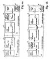
- FIGS. 1 a and 1 bare block diagrams of alternative configurations of a display system of one embodiment of the invention.
- FIG. 2is a block diagram of a display system of one embodiment of the invention.
- FIG. 3is an exemplary state diagram of one embodiment of the state machine.
- FIG. 4is a block diagram of a safety timer of one embodiment of the invention.
- FIG. 5is a schematic of a safety timer of one embodiment of the invention.
- FIGS. 1 a and 1 bare block diagrams of alternative configurations of a display system of one embodiment of the invention.
- a video source subsystem 10includes a video source 12 coupled to a low voltage differential signaling (LVDS) transmitter 14 .
- LVDS transmitters and receiversare commercially available, and LVDS signaling is generally well-known in the art.
- a video signal from the video source 12is converted by the LVDS transmitter and transmitted in a standard manner across a cable to an LVDS receiver 22 in headset subsystem 20 .
- a display controller with embedded memory 24receives the output of the LVDS receiver 22 and stores the subframes of the image data in the embedded memory. Subframes are then sent out to display chip 26 which is also within the headset subsystem 20 .
- a high voltage platform 28 within the headset subsystem 20is coupled to the display chip 26 and responsible for driving the cover glass voltage (CGV) of the display.
- the CGVmay be driven from the display substrate.
- the CGV rangecould be restricted to be driven by a voltage range that can be supplied directly from the display substrate such as 0 to 5 volts.
- FIG. 1 bshows a system employing the same components in a slightly different configuration.
- video source subsystem 30has video source 12 coupled to display controller with memory 24 (possibly embedded) which in turn provides its output to the LVDS transmitter 14 to be cabled to the LVDS receiver 22 in the headset subsystem 40 .
- the display chip 26then receives the output of the LVDS receiver 22 and is supplied power in the same manner by high voltage platform 28 as described with reference to FIG. 1 a above.
- the flexibility of the display controller and memory 24 to provide or receive LVDS signaling and also the display chip 26 to receive LVDS signalingpermits significant flexibility in system design.
- Co-pending U.S. patent application No. 09/222,230, filed Dec. 29, 1998describes an example of a display which may be used with embodiments of the invention, including the systems of FIG. 1 a or 1 b ; that application is hereby incorporated by reference.
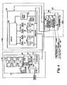
- FIG. 2is a block diagram of a display system of one embodiment of the invention.
- LVDS transmitters and receiversare not shown, but it is within the scope and contemplation of the invention to configure the system of FIG. 2 as shown in 1 a or 1 b , or the LVDS components may be omitted entirely.
- the systemis segregated into three distinct power zones, 100 , 200 , 300 .
- Power zone 200includes a substrate 202 which has a display 204 formed thereon.
- display 204is a liquid crystal on silicon (LCOS) display.
- DACsdigital to analog converters
- a set of control registers 214are formed on substrate 202 and used to control the function of the other devices formed on substrate 202 and also provide control signals to a high-power platform in power zone 300 .
- a safety timer 212is formed on a substrate 202 . Safety timer 212 is used to drive the display into a safe state in the event of certain system malfunctions. Safety timer 212 is described in further detail with respect to FIGS. 4 and 5 below.
- Interface 210 formed on substrate 202may be a LVDS compliant interface and is responsible for directing incoming data appropriately to the LUTs 208 or the control register space 214 .
- the control register spaceincludes registers required to manage display functions and registers to hold control information to be sent to substrate 302 (discussed below).
- the control registersare a DAC standby register to power and remove power from the DACs, a start of frame registers to signal the start of a new frame, LED enable register, and a cover glass voltage register. Additional useful registers will occur to one of ordinary skill in the art.
- the display 204occupies 80-90% of the die space of substrate 202 . It operates at a 5 V level and is driven by TTL level outputs.
- the formation of the devices on substrate 202should be formed with a process having a feature size compatible with these needs. It has been found that 0.8 ⁇ feature size is satisfactory. For even lower power consumption, a 0.45 ⁇ feature size could be used for substrate 202 , while still maintaining 5 V operation if desired.
- Substrate 202is coupled to a substrate 302 which resides in power zone 300 .
- Substrate 302is manufactured with a much larger feature size because of its voltage requirements.
- the cover glass voltage (CGV) generator 306generates the voltage for the cover glass of the display 204 .
- the cover glass voltage requirementsdictate that it be driven between a +6 V and ⁇ 2 V.
- CGV generator 306To supply this range, a larger feature size needs to be employed in the formation of CGV generator 306 .
- a 3 ⁇ processhas been found suitable.
- an LED driver 308Also on substrate 302 is part of an LED driver 308 which enables the red, green and blue LEDs which illuminate the display 204 in a time sequential manner. Because it uses a significantly larger process, operations on substrate 302 occur at a much slower rate than, for example, on substrate 202 . Moreover, for space reasons, it is desirable to keep the circuitry on substrate 302 to a minimum.
- a simple data interfaceexists between substrate 202 and substrate 302 consisting of three lines, a data-in line, a clock line, and a load line.
- Control register 304is shown exploded out. It contains three LED enables, Red Enable 312 , Green Enable 314 , and Blue Enable 316 . These values are provided to the LED driver 308 and are the basis on which the LED driver 308 drives the corresponding LEDs.
- CGV 318is a ten bit value that is provided to the CGV generator 306 from which the CGV generator 306 generates the appropriate voltage for the cover glass over substrate 202 .
- a final bit of control register 304is the power bit 320 which causes substrate 302 to be powered or not powered, depending on whether the power bit is active.
- Display controller substrate 102is Also coupled to the substrate 202 .
- a coupling of substrate 102 to substrate 202may be local or via cable through a pair of LVDS interfaces.
- Substrate 102includes a logic unit 104 which functions as a display controller for the display.
- the logic unit 104includes a state machine 106 which drives data in a color sequential manner to the display.
- a parser 108may also be provided which accepts data in an RGB format and converts it to a parallelization of R, and then G, and then B.
- a storage unit 116which may be embedded dynamic random access memory (DRAM), is also formed on substrate 102 .
- a storage unitshould include at least two logically distinct subunits.
- the FIFOmust be large enough to supply sufficient subframe data while the incoming image frame occupies the memory interface. Additionally, relatively large FIFOs must be supplied on the incoming side to hold the data while the output side (or another subunit of the input side) is being serviced. Even with the parser present such that the data is stored in separate logical storage areas, first red, then green, then blue, the complexity of the memory controller and FIFO is required for each subunit increase in both power usage and die space. In this example, the memory controller would need to handle four data streams (three in, one out) with different clock rates between the streams in and the streams out.
- memory accessis significantly simplified such that a simpler memory controller may be employed, smaller or no FIFOs may be used, and the memory to outgoing FIFO operational speed can be significantly reduced.
- storage unit 116is shown composed of six subunits 120 and 118 . Each subunit is presumed to have it own independent memory interface in this embodiment of the invention. Because a frame will be displayed simultaneously with one being loaded, the system ping pongs back and forth between subunits 118 and subunits 120 for loading/displaying.
- a LUT data storage unit 114which may be part of storage unit 116 or formed as a separate memory type, such as SRAM, is also provided. LUT data storage 114 retains six LUT data sets, one corresponding to each of R, G, B, ⁇ overscore (R) ⁇ , ⁇ overscore (G) ⁇ , ⁇ overscore (B) ⁇ .
- Another embodimentpermits the system to use an inverted LUT data set rather than inverting the data itself, providing greater flexibility in the inverting algorithm.
- Another embodimentpermits the use of only three LUT data sets R, G, and B with inverses generated by logic 106 . In such embodiments, a small amount of storage is saved at a cost of more stringent DAC linearity requirements.
- interfaces 110 and 112are both LVDS compliant, allowing greater flexibility in the positioning of the controller relative to the display.
- Interface 110may optionally provide conversion from a YUV format to RGB format.
- either interface 110 or parser 108truncates incoming color data by dropping the two least significant bits thereby changing the resolution from eight bits per color to six bits per color, as stored in a storage unit 116 .
- Thispermits the controller chip to send four pixels (of six bits each) simultaneously to the display chip using standard LVDS techniques.
- the lookup tablethen maps the six bits into eight bits.
- a set of LUT datais basically a listing of output codes that correspond to each possible input code. Since the shown embodiment uses six bit input code, that implies 64 output codes selected from a 256 possible output codes.
- the embodiment abovedescribes a six to eight bit encoding through the LUT, it is within the scope and contemplation of the invention to perform other encodings.
- a two to eight encodingwould permit four colors to be selected from a very large palette and permit extremely high speed pixel throughput as twelve pixels could be processed simultaneously using the current 24 bit data path, assuming the twelve LUTs and twelve DACs are also provided.
- the output codingmay be greater than eight bits. Such merely increases the size of the LUT data set and provides a larger palette from which to select output codes.
- a first frameis loaded into, for example, subunits 118 as three distinct subframes, e.g. a red subframe, a green subframe, and a blue subframe.
- a state machine 106then begins feeding the subframes to the display substrate 202 preceded by an appropriate LUT data set.
- the 24 data signals moving between controller substrate 102 and display substrate 202there are also a mode signal, a reset signal, a clock signal, and a chipselect signal.
- the chipselect signalpermits the display controller to drive multiple displays by selecting only the one to which the frame should be sent.
- the mode signalselects between a register mode and a data mode. In data mode, four pixels of data are moved across the 24 lines on each clock.
- the data linesbecome nine address lines, eight data lines, a read line and a write line (with five lines unused). It is in register mode that LUT writes and register writes occur. It will be recognized that these twenty-eight signals are readily transferred using LVDS techniques.
- the LUTis loaded first with an appropriate LUT data set corresponding to the immediately following subframe and provides the necessary mapping of six bit color data to eight bit display data.
- the LUT data setis selected to accommodate for non-linearities in the DACs 206 and the liquid crystal response to the particular color. LUTs may also be used to perform gamma correction, for example. While to first order, e.g. R and ⁇ overscore (R) ⁇ LUT data sets are true inverses of each other, in reality, secondary effects such as the difference in non-linearity of the liquid crystal or the DAC when exposed to a negative voltage may require greater difference between the positive and inversed LUT data set. This ability to compensate for these differences provides improved image quality of standard frame inversion techniques.
- the color datais applied to the LUTs with one pixel to each LUT, thus, four pixels (in the same monochrome subframe) are processed simultaneously and then driven by the DACs onto the display. An entire subframe is driven to the display after which the display is illuminated by the corresponding LED color. Subsequently, the other two subframes are in turn driven to the display and illuminated. It should be recognized that the particular ordering of the red, green, blue subframes may be arbitrary. Additionally, it is desirable, when driving a liquid crystal display, to toggle between driving a positive subframe and driving an inverse subframe to protect the display from deleterious effects of constant voltage difference conditions. Accordingly, as mentioned above, the LUT data set selected to be driven to the LUT will alternate between a positive data set and an inverse data set.
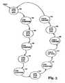
- FIG. 3shows an exemplary state diagram of one embodiment of state machine 106 .
- the state machineUpon reset, the state machine enters a load R LUT data state. In this state, the LUT data set corresponding to R is loaded into the LUT on substrate 202 .
- the four LUTsreceive the same LUT data for the red subframe in order to drive four separate pixels.
- the substrate 202would include the same (e.g. one) number of LUTs.
- a state machinethen advances to the load R subframe state 404 .
- the R data from the logically distinct R buffer in storage unit 116is passed through the LUTs and the corresponding values driven to corresponding pixels on the display 204 .
- the statethen advances to the load ⁇ overscore (G) ⁇ LUT data state 406 .
- the LUTs on substrate 202are loaded with a data set corresponding to ⁇ overscore (G) ⁇ .
- the G subframeis then driven to the LUTs and the corresponding encoding is driven to the display four pixels at a time.
- the LUTsare loaded with a B LUT data set and the state advances to the load B subframe 412 .
- the B subframeis driven to the display.
- the human eyeintegrates the subframe to perceive a full color image.
- the incoming and outgoing subunits of storage unit 116swap for the next series of states.
- the ⁇ overscore (R) ⁇ LUT data setis then loaded into the LUTs at state 414 and a next red subframe (in this case, from R subbuffer 120 ) is driven through the LUTs and DACs to the display at state 416 .
- the stateadvances to state 418 in which the G LUT data set is loaded into the LUTs.
- the statethen advances to 420 and the G subframe from G subbuffer 120 is driven to the display, and so forth, at states 422 and 424 for the ⁇ overscore (B) ⁇ LUT data and the corresponding B subframe.
- the state machine 104then returns to state 402 and begins driving R LUT data again, as long as state machine 104 remains in the active displaying mode.
- parser 108allows the subbuffer, e.g. 118 , to be randomly written with new pixel data during the times when the subbuffer is not being accessed to provide data to the display. In this case, the same order as described above with reference to FIG. 3 occurs, but no swap of subbuffers is used. This ordering is repeated over and over, allowing input access during the non-displaying time.
- one embodiment of the inventionmight use one group of LUT data sets R 1 ,G 1 , B 1 , ⁇ overscore (R) ⁇ 1 , ⁇ overscore (G) ⁇ 1 , ⁇ overscore (B) ⁇ 1 , for temperatures below a certain threshold and a second group R 2 , G 2 , B 2 , ⁇ overscore (R) ⁇ 2 , ⁇ overscore (G) ⁇ 2 , ⁇ overscore (B) ⁇ 2 , for temperatures above the threshold.
- the corresponding state machinewould look like FIG. 3 duplicated with temperature selecting the loop of states through which the state machine transitions.
- different groups of data setsmay be used for different frame rates or different contrast settings, environmental conditions, liquid crystal, etc.
- Other bases for using multiple groups of data setsare also within the scope and contemplation of the invention.
- the LUT data setsmay require R, G, B and no inverted sets.
- faultmeans anything affecting the status of the circuitry or software driving the display or the display itself.
- a number of problemsmay occur that cause the display to become hung up with a constant CGV and a DC voltage across the liquid crystal. Even with small voltage differences between the cover glass and the underlying pixels, damage may occur to the liquid crystal. Examples of fault that my occur include a crash of the display controller or the host video source that causes the display controller to leave its display state machine with the subframe unfinished. Hot plugging the cable or improperly coupling the cable may also cause the system to hang.
- the safety timeras described below can be used to drive the display into a safe state in the event of potentially damaging faults. Because a pathological condition that causes the power to the display to be wholly disrupted is also a “safe state” for the display, the safety timer need only address the conditions during which power is supplied to the display chip substrate.
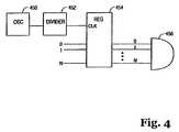
- FIG. 4shows a block diagram of a safety timer of one embodiment of the invention.
- An oscillator 450independent of the clock that drives the remainder of the display chip is employed to provide the safety timer clock.
- a clock divider 452may optionally be employed to expand the period during which indicators of proper function will be collected from the fundamental frequency of the oscillator.
- An arbitrarily large number of indicators (0-N)may be collected during the period and stored in a register 454 or series of flip flops. Individual register positions are then effectively ANDed together or an expected set of indicators may be compared with a set of indicators actually received. Other methods of determining if all indicators have been received are within the scope and contemplation of the invention. If all the indicators are received during the specified period, the system is then deemed to be working properly.
- a safe stateis defined in one embodiment as having a CGV of zero volts and all the pixels driven to zero volts. Reset, the safe state, is maintained until all the indicators are collected during an appropriate time period. Thus, if the deficiency is a permanent condition, the reset will be permanently maintained until the system is fixed. If the failure to receive an indicator is transient, possibly on the next oscillator cycle, the reset will be released. Significantly, it is important during reset to allow the interface 210 on substrate 202 to continue to receive signals, otherwise, a timer will never come out of reset.
- FIG. 5shows a schematic of a safety timer of one embodiment of the invention.
- a plurality of indicators, IND0 through IND5are fed into combinational logic 506 .
- the indicatorsmay be signals available in raw form on the display chip or signals derived from additional combinational logic (not shown) that is also formed on the display chip.
- the results of combinational logic 506are retained in flip flops 502 and combined by NAND gate 512 for storage of a single signal in flip flop 504 .
- the independent oscillator 500provides all clocking for the safety timer circuit.
- Oscillator 500includes a divider circuit which is driven by T signals 508 .
- the T signalis a two bit signal which provides four possible clock periods from oscillator 500 .
- the T signalmay be provided by a register in the register space.
- the power on reset (POR) circuit 510is also provided to ensure that the safety timer provides a reset at power on and allows the system to stabilize before releasing the reset or safety mode.
- PORpower on reset
- all register values on the display chipreturn to default values when the timer comes out of reset. This is desirable because it is assumed that a pathological condition usually causes the timer to force the chip into safe mode, or reset. Thus, it is reasonable to presume that there may have been some corruption of register values during that pathological condition. By returning the registers to default values, any corrupted values are overwritten.
- a hard wired enable (HW_ENB)is supplied so that the timer can be permanently disabled if desired for a particular application or system.
- Safety timer enable (ST 13 ENB)may be used to temporarily disable the safety timer when such is desired, as is certain test cases.
- IND0, IND1, and IND5collectively, indicate whether a write to any register in the control register space of the display chip has occurred.
- IND2, IND3, and IND4reflect whether a write to specific registers in the control register block has occurred.
- IND2may indicate whether the load register for the high voltage platform has been written to
- IND3might indicate whether a frame start register has been written to
- IND4might indicate whether a standby register has been written.
- the standby registercauses the DACs to power down when not physically driving data to the display. This is desirable because the DACs consume a significant amount of power and also running constantly may exhibit undesirable heat characteristics.
- indicatorsare selected so that at least one indicator is provided along each channel of the LVDS cable. This has the advantage of permitting identification of errors related to damage to a single channel, for example, as a result of kinking of the cable.
- the above-described embodimentrelies on register writes as the basis for operation of the safety timer.
- Other suitable indicatorsinclude pixel clock activity, LUT writes, selected data wires, and even cover glass switching. It is, of course, possible in principle to examine every incoming signal to ensure that all expected signals are received during each frame. However, that becomes unjustifiably overhead intensive with corresponding circuit size and power costs.
- a safety timercan be effectively implemented which protects the display subsystem from permanent damage as a result of those faults.
- the timerdoes not merely identify the existence of a fault condition and report, e.g. to the display controller, for corrective action. Rather, the safety timer drives the reset signal that places the display in a safe state.
Landscapes
- Engineering & Computer Science (AREA)
- Theoretical Computer Science (AREA)
- Physics & Mathematics (AREA)
- General Physics & Mathematics (AREA)
- Computer Hardware Design (AREA)
- Human Computer Interaction (AREA)
- General Engineering & Computer Science (AREA)
- Chemical & Material Sciences (AREA)
- Crystallography & Structural Chemistry (AREA)
- Control Of Indicators Other Than Cathode Ray Tubes (AREA)
- Image Processing (AREA)
Abstract
Description
Claims (17)
Priority Applications (1)
| Application Number | Priority Date | Filing Date | Title |
|---|---|---|---|
| US09/989,764US6744443B2 (en) | 1996-12-19 | 2001-11-19 | Time sequential lookup table method for a display |
Applications Claiming Priority (8)
| Application Number | Priority Date | Filing Date | Title |
|---|---|---|---|
| US08/770,233US5920298A (en) | 1996-12-19 | 1996-12-19 | Display system having common electrode modulation |
| US08/801,994US6078303A (en) | 1996-12-19 | 1997-02-18 | Display system having electrode modulation to alter a state of an electro-optic layer |
| US08/920,603US6144353A (en) | 1996-12-19 | 1997-08-27 | Display system having electrode modulation to alter a state of an electro-optic layer |
| US08/920,602US6104367A (en) | 1996-12-19 | 1997-08-27 | Display system having electrode modulation to alter a state of an electro-optic layer |
| US08/994,033US6046716A (en) | 1996-12-19 | 1997-12-18 | Display system having electrode modulation to alter a state of an electro-optic layer |
| US09/312,196US6373497B1 (en) | 1999-05-14 | 1999-05-14 | Time sequential lookup table arrangement for a display |
| US09/542,432US6329971B2 (en) | 1996-12-19 | 2000-04-04 | Display system having electrode modulation to alter a state of an electro-optic layer |
| US09/989,764US6744443B2 (en) | 1996-12-19 | 2001-11-19 | Time sequential lookup table method for a display |
Related Parent Applications (4)
| Application Number | Title | Priority Date | Filing Date |
|---|---|---|---|
| US08/770,233Continuation-In-PartUS5920298A (en) | 1996-12-19 | 1996-12-19 | Display system having common electrode modulation |
| US09/312,196ContinuationUS6373497B1 (en) | 1996-12-19 | 1999-05-14 | Time sequential lookup table arrangement for a display |
| US09/542,432Continuation-In-PartUS6329971B2 (en) | 1996-12-19 | 2000-04-04 | Display system having electrode modulation to alter a state of an electro-optic layer |
| US09/989,764ContinuationUS6744443B2 (en) | 1996-12-19 | 2001-11-19 | Time sequential lookup table method for a display |
Related Child Applications (2)
| Application Number | Title | Priority Date | Filing Date |
|---|---|---|---|
| US08/994,033Continuation-In-PartUS6046716A (en) | 1996-12-19 | 1997-12-18 | Display system having electrode modulation to alter a state of an electro-optic layer |
| US09/989,764ContinuationUS6744443B2 (en) | 1996-12-19 | 2001-11-19 | Time sequential lookup table method for a display |
Publications (2)
| Publication Number | Publication Date |
|---|---|
| US20020030691A1 US20020030691A1 (en) | 2002-03-14 |
| US6744443B2true US6744443B2 (en) | 2004-06-01 |
Family
ID=23210312
Family Applications (2)
| Application Number | Title | Priority Date | Filing Date |
|---|---|---|---|
| US09/312,196Expired - LifetimeUS6373497B1 (en) | 1996-12-19 | 1999-05-14 | Time sequential lookup table arrangement for a display |
| US09/989,764Expired - LifetimeUS6744443B2 (en) | 1996-12-19 | 2001-11-19 | Time sequential lookup table method for a display |
Family Applications Before (1)
| Application Number | Title | Priority Date | Filing Date |
|---|---|---|---|
| US09/312,196Expired - LifetimeUS6373497B1 (en) | 1996-12-19 | 1999-05-14 | Time sequential lookup table arrangement for a display |
Country Status (5)
| Country | Link |
|---|---|
| US (2) | US6373497B1 (en) |
| EP (1) | EP1190412A1 (en) |
| JP (1) | JP2002544573A (en) |
| AU (1) | AU5006400A (en) |
| WO (1) | WO2000070598A1 (en) |
Cited By (3)
| Publication number | Priority date | Publication date | Assignee | Title |
|---|---|---|---|---|
| WO2007041839A1 (en)* | 2005-10-13 | 2007-04-19 | Vincent So | Image display methods and systems with sub-frame intensity compensation |
| US7634134B1 (en) | 2004-03-15 | 2009-12-15 | Vincent So | Anti-piracy image display methods and systems |
| US20100149221A1 (en)* | 2008-12-16 | 2010-06-17 | Chunghwa Picture Tubes, Ltd. | Drive current of light source by color sequential method |
Families Citing this family (33)
| Publication number | Priority date | Publication date | Assignee | Title |
|---|---|---|---|---|
| US6373497B1 (en)* | 1999-05-14 | 2002-04-16 | Zight Corporation | Time sequential lookup table arrangement for a display |
| US6768774B1 (en)* | 1998-11-09 | 2004-07-27 | Broadcom Corporation | Video and graphics system with video scaling |
| US6853385B1 (en)* | 1999-11-09 | 2005-02-08 | Broadcom Corporation | Video, audio and graphics decode, composite and display system |
| US6661422B1 (en)* | 1998-11-09 | 2003-12-09 | Broadcom Corporation | Video and graphics system with MPEG specific data transfer commands |
| US6798420B1 (en)* | 1998-11-09 | 2004-09-28 | Broadcom Corporation | Video and graphics system with a single-port RAM |
| US6573905B1 (en)* | 1999-11-09 | 2003-06-03 | Broadcom Corporation | Video and graphics system with parallel processing of graphics windows |
| US7982740B2 (en) | 1998-11-09 | 2011-07-19 | Broadcom Corporation | Low resolution graphics mode support using window descriptors |
| US6636222B1 (en)* | 1999-11-09 | 2003-10-21 | Broadcom Corporation | Video and graphics system with an MPEG video decoder for concurrent multi-row decoding |
| US6731295B1 (en)* | 1998-11-09 | 2004-05-04 | Broadcom Corporation | Graphics display system with window descriptors |
| US7446774B1 (en) | 1998-11-09 | 2008-11-04 | Broadcom Corporation | Video and graphics system with an integrated system bridge controller |
| US6803885B1 (en) | 1999-06-21 | 2004-10-12 | Silicon Display Incorporated | Method and system for displaying information using a transportable display chip |
| US6975324B1 (en) | 1999-11-09 | 2005-12-13 | Broadcom Corporation | Video and graphics system with a video transport processor |
| US6545672B1 (en)* | 2000-07-19 | 2003-04-08 | Hewlett Packard Development Company, L.P. | Method and apparatus for avoiding image flicker in an optical projection display |
| JP3770380B2 (en)* | 2000-09-19 | 2006-04-26 | シャープ株式会社 | Liquid crystal display |
| US6909435B2 (en)* | 2000-12-20 | 2005-06-21 | Thomson Licensing S.A. | Reduction of gamma correction contouring in liquid crystal on silicon (LCOS) displays |
| JP2002218345A (en)* | 2001-01-16 | 2002-08-02 | Mitsubishi Electric Corp | Screen display device |
| GB2375447B (en)* | 2001-05-10 | 2005-06-08 | Amulet Electronics Ltd | Encoding digital video for transmission over standard data cabling |
| US6972778B2 (en) | 2002-06-27 | 2005-12-06 | Koninklijke Philips Electronics N.V. | Color re-mapping for color sequential displays |
| JP2004053715A (en)* | 2002-07-17 | 2004-02-19 | Sanyo Electric Co Ltd | Display device and its gamma correction method |
| EP1579411B1 (en)* | 2002-12-20 | 2012-10-10 | Trident Microsystems (Far East) Ltd. | Apparatus for re-ordering video data for displays using two transpose steps and storage of intermediate partially re-ordered video data |
| US8326483B2 (en) | 2003-02-21 | 2012-12-04 | Gentex Corporation | Monitoring and automatic equipment control systems |
| JP4846571B2 (en)* | 2003-04-24 | 2011-12-28 | ディスプレイテック,インコーポレイテッド | Microdisplay system and image display method |
| US7071908B2 (en)* | 2003-05-20 | 2006-07-04 | Kagutech, Ltd. | Digital backplane |
| US8063916B2 (en) | 2003-10-22 | 2011-11-22 | Broadcom Corporation | Graphics layer reduction for video composition |
| JP2005316146A (en)* | 2004-04-28 | 2005-11-10 | Fujitsu Display Technologies Corp | Liquid crystal display device and processing method thereof |
| EP1756799A4 (en)* | 2004-05-19 | 2008-06-11 | Sharp Kk | Liquid crystal display device, driving method thereof, liquid crystal television having the liquid crystal display device and liquid crystal monitor having the liquid crystal display device |
| JP2006030783A (en)* | 2004-07-20 | 2006-02-02 | Alps Electric Co Ltd | Liquid crystal display device |
| US7696990B2 (en)* | 2006-06-28 | 2010-04-13 | Harvatek Corporation | LED driving circuit and a serial LED illumination system using the same |
| WO2008086222A2 (en)* | 2007-01-04 | 2008-07-17 | Displaytech, Inc | Digital display |
| US20090040167A1 (en)* | 2007-08-06 | 2009-02-12 | Wein-Town Sun | Programmable nonvolatile memory embedded in a timing controller for storing lookup tables |
| JP2012133070A (en)* | 2010-12-21 | 2012-07-12 | Sanyo Engineer & Construction Inc | Driving circuit of lcos element |
| WO2022170135A1 (en) | 2021-02-05 | 2022-08-11 | Boulder Nonlinear Systems, Inc. | Simultaneous focusing of an optical system to multiple focal planes using liquid crystal polarization lenses |
| CN113778306A (en)* | 2021-09-07 | 2021-12-10 | 上海浦东发展银行股份有限公司 | Table data processing method, device, equipment and storage medium |
Citations (18)
| Publication number | Priority date | Publication date | Assignee | Title |
|---|---|---|---|---|
| US5355443A (en)* | 1990-06-04 | 1994-10-11 | University Of Washington | Image computing system |
| EP0707305A2 (en) | 1994-10-12 | 1996-04-17 | Canon Kabushiki Kaisha | Display mode detector, pixel clock synchroniser and interpolator for ferroelectric liquid crystal display |
| EP0745969A2 (en) | 1995-06-02 | 1996-12-04 | Canon Kabushiki Kaisha | Display control apparatus for a display system |
| US5673058A (en)* | 1988-10-31 | 1997-09-30 | Hitachi, Ltd. | One-chip semiconductor integrated circuit device capable of outputting analog color signal or digital color signal |
| US5699076A (en)* | 1993-10-25 | 1997-12-16 | Kabushiki Kaisha Toshiba | Display control method and apparatus for performing high-quality display free from noise lines |
| US5717697A (en)* | 1990-06-27 | 1998-02-10 | Texas Instruments Incorporated | Test circuits and methods for integrated circuit having memory and non-memory circuits by accumulating bits of a particular logic state |
| US5736137A (en) | 1992-11-13 | 1998-04-07 | Idec Pharmaceuticals Corporation | Therapeutic application of chimeric and radiolabeled antibodies to human B lymphocyte restricted differentiation antigen for treatment of B cell lymphoma |
| US5801665A (en)* | 1995-10-30 | 1998-09-01 | Industrial Technology Research Institute | Format converter for the conversion of conventional color display format to field sequential |
| EP0875881A2 (en) | 1997-04-30 | 1998-11-04 | SHARP Corporation | Active matrix light modulators, use of an active matrix light modulator, and display |
| US5838389A (en)* | 1992-11-02 | 1998-11-17 | The 3Do Company | Apparatus and method for updating a CLUT during horizontal blanking |
| US5867134A (en)* | 1995-08-25 | 1999-02-02 | Alvelda; Phillip | VLSI visual display |
| EP0915361A1 (en) | 1997-04-22 | 1999-05-12 | Matsushita Electric Industrial Co., Ltd. | Drive circuit for active matrix liquid crystal display |
| US5959598A (en)* | 1995-07-20 | 1999-09-28 | The Regents Of The University Of Colorado | Pixel buffer circuits for implementing improved methods of displaying grey-scale or color images |
| US6046716A (en)* | 1996-12-19 | 2000-04-04 | Colorado Microdisplay, Inc. | Display system having electrode modulation to alter a state of an electro-optic layer |
| US6097362A (en)* | 1997-10-14 | 2000-08-01 | Lg Semicon Co., Ltd. | Driver for liquid crystal display |
| US6108000A (en)* | 1997-03-05 | 2000-08-22 | Microdisplay Corporation | Resonant driver apparatus and method |
| US6166724A (en)* | 1998-10-05 | 2000-12-26 | Ati International Srl | Method and apparatus for sequencing palette updates in a video graphics system |
| US6373497B1 (en)* | 1999-05-14 | 2002-04-16 | Zight Corporation | Time sequential lookup table arrangement for a display |
- 1999
- 1999-05-14USUS09/312,196patent/US6373497B1/ennot_activeExpired - Lifetime
- 2000
- 2000-05-12EPEP00932326Apatent/EP1190412A1/ennot_activeWithdrawn
- 2000-05-12WOPCT/US2000/012983patent/WO2000070598A1/ennot_activeApplication Discontinuation
- 2000-05-12JPJP2000618967Apatent/JP2002544573A/enactivePending
- 2000-05-12AUAU50064/00Apatent/AU5006400A/ennot_activeAbandoned
- 2001
- 2001-11-19USUS09/989,764patent/US6744443B2/ennot_activeExpired - Lifetime
Patent Citations (18)
| Publication number | Priority date | Publication date | Assignee | Title |
|---|---|---|---|---|
| US5673058A (en)* | 1988-10-31 | 1997-09-30 | Hitachi, Ltd. | One-chip semiconductor integrated circuit device capable of outputting analog color signal or digital color signal |
| US5355443A (en)* | 1990-06-04 | 1994-10-11 | University Of Washington | Image computing system |
| US5717697A (en)* | 1990-06-27 | 1998-02-10 | Texas Instruments Incorporated | Test circuits and methods for integrated circuit having memory and non-memory circuits by accumulating bits of a particular logic state |
| US5838389A (en)* | 1992-11-02 | 1998-11-17 | The 3Do Company | Apparatus and method for updating a CLUT during horizontal blanking |
| US5736137A (en) | 1992-11-13 | 1998-04-07 | Idec Pharmaceuticals Corporation | Therapeutic application of chimeric and radiolabeled antibodies to human B lymphocyte restricted differentiation antigen for treatment of B cell lymphoma |
| US5699076A (en)* | 1993-10-25 | 1997-12-16 | Kabushiki Kaisha Toshiba | Display control method and apparatus for performing high-quality display free from noise lines |
| EP0707305A2 (en) | 1994-10-12 | 1996-04-17 | Canon Kabushiki Kaisha | Display mode detector, pixel clock synchroniser and interpolator for ferroelectric liquid crystal display |
| EP0745969A2 (en) | 1995-06-02 | 1996-12-04 | Canon Kabushiki Kaisha | Display control apparatus for a display system |
| US5959598A (en)* | 1995-07-20 | 1999-09-28 | The Regents Of The University Of Colorado | Pixel buffer circuits for implementing improved methods of displaying grey-scale or color images |
| US5867134A (en)* | 1995-08-25 | 1999-02-02 | Alvelda; Phillip | VLSI visual display |
| US5801665A (en)* | 1995-10-30 | 1998-09-01 | Industrial Technology Research Institute | Format converter for the conversion of conventional color display format to field sequential |
| US6046716A (en)* | 1996-12-19 | 2000-04-04 | Colorado Microdisplay, Inc. | Display system having electrode modulation to alter a state of an electro-optic layer |
| US6108000A (en)* | 1997-03-05 | 2000-08-22 | Microdisplay Corporation | Resonant driver apparatus and method |
| EP0915361A1 (en) | 1997-04-22 | 1999-05-12 | Matsushita Electric Industrial Co., Ltd. | Drive circuit for active matrix liquid crystal display |
| EP0875881A2 (en) | 1997-04-30 | 1998-11-04 | SHARP Corporation | Active matrix light modulators, use of an active matrix light modulator, and display |
| US6097362A (en)* | 1997-10-14 | 2000-08-01 | Lg Semicon Co., Ltd. | Driver for liquid crystal display |
| US6166724A (en)* | 1998-10-05 | 2000-12-26 | Ati International Srl | Method and apparatus for sequencing palette updates in a video graphics system |
| US6373497B1 (en)* | 1999-05-14 | 2002-04-16 | Zight Corporation | Time sequential lookup table arrangement for a display |
Non-Patent Citations (11)
| Title |
|---|
| Ammer, J., Bolotski, M., Alvelda, P., Knight, Jr. T., "A 160x120 Pixel Liquid-Crystal-on-Silicon Microdisplay with an Adiabatic DACM", 1999 IEEE International Solid-State Circuits Conference, pp. 212-213.** |
| Ammer, J., Bolotski, M., Alvelda, P., Knight, Jr. T., "A 160×120 Pixel Liquid-Crystal-on-Silicon Microdisplay with an Adiabatic DACM", 1999 IEEE International Solid-State Circuits Conference, pp. 212-213.* |
| Ammer, J., et al. "A 160x120 Pixel Liquid-Crystal -on-Silicon Microdisplay with an Adiabatic DACM", 1999 IEEE International Solid State Circuits Conference, pp. 212-213.** |
| Ammer, J., et al. "A 160×120 Pixel Liquid-Crystal -on-Silicon Microdisplay with an Adiabatic DACM", 1999 IEEE International Solid State Circuits Conference, pp. 212-213.* |
| Bolotski, M., Alvelda, P., "Low-Power Miniaturized Information Display Systems", ISLPED 98, Aug. 1998, pp. 279-281.** |
| Cheng, P., Huang, H., "Electronics Development of Silicon Microdisplays for Virtual Reality Applications", Proceedings of the ASP-DAC '99, 1999, pp. 197-200.** |
| MicroDisplay Press Release, "The MicroDisplay Corporation Makes Display Integration Breakthrough", Jul. 1998.** |
| PCT International Search Report for PCT Application No. PCT/US00/012983, mailed Sep. 11, 2000. |
| Schuck, M., McKnight, D., Johnson K., "Smart Pixel LCOS devices for Projection Display Systems", IEEE/LEOS 1996 Summer Topical Meetings, 1996, pp. 11-12.** |
| Underwood, Ian, "VLSI Design and Fabrication for Liquid-Crystal on Silicon", IEE Seminar on Microdisplay and Smart Pixel Technologies, 2000, pp. 7/1-7/6.** |
| Underwood, Ian, "VLSI Design and Fabrication for Liquid-Cystal on Silicon", IEE Seminar on Microdisplay and Smart Pixel Technologies, 2000, pp. 7/1-7/6.** |
Cited By (7)
| Publication number | Priority date | Publication date | Assignee | Title |
|---|---|---|---|---|
| US7634134B1 (en) | 2004-03-15 | 2009-12-15 | Vincent So | Anti-piracy image display methods and systems |
| US7693330B2 (en) | 2004-03-15 | 2010-04-06 | Vincent So | Anti-piracy image display methods and systems with sub-frame intensity compensation |
| US20100142912A1 (en)* | 2004-03-15 | 2010-06-10 | Vincent So | Image display methods and systems with sub-frame intensity compensation |
| US7865034B2 (en)* | 2004-03-15 | 2011-01-04 | Vincent So | Image display methods and systems with sub-frame intensity compensation |
| WO2007041839A1 (en)* | 2005-10-13 | 2007-04-19 | Vincent So | Image display methods and systems with sub-frame intensity compensation |
| US20100149221A1 (en)* | 2008-12-16 | 2010-06-17 | Chunghwa Picture Tubes, Ltd. | Drive current of light source by color sequential method |
| US8259060B2 (en) | 2008-12-16 | 2012-09-04 | Chunghwa Picture Tubes, Ltd. | Drive current of light source by color sequential method |
Also Published As
| Publication number | Publication date |
|---|---|
| WO2000070598A1 (en) | 2000-11-23 |
| EP1190412A1 (en) | 2002-03-27 |
| US20020030691A1 (en) | 2002-03-14 |
| JP2002544573A (en) | 2002-12-24 |
| AU5006400A (en) | 2000-12-05 |
| US6373497B1 (en) | 2002-04-16 |
Similar Documents
| Publication | Publication Date | Title |
|---|---|---|
| US6744443B2 (en) | Time sequential lookup table method for a display | |
| US6356260B1 (en) | Method for reducing power and electromagnetic interference in conveying video data | |
| US7660010B2 (en) | Controller driver, liquid crystal display apparatus using the same, and liquid crystal driving method | |
| US6628243B1 (en) | Presenting independent images on multiple display devices from one set of control signals | |
| US10762827B2 (en) | Signal supply circuit and display device | |
| US7742065B2 (en) | Controller driver and liquid crystal display apparatus using the same | |
| US5790136A (en) | Interleaving pixel data for a memory display interface | |
| EP1649445A2 (en) | Microdisplay and interface on a single chip | |
| US20060256063A1 (en) | Display apparatus including source drivers and method of controlling clock signals of the source drivers | |
| GB2366439A (en) | Driving arrangements for active matrix LCDs | |
| US11837143B2 (en) | Display apparatus and a method of driving the same | |
| EP0231612A2 (en) | A method and apparatus for accessing a memory in a colour graphics system | |
| US6326958B1 (en) | Power partitioned miniature display system | |
| US6448962B1 (en) | Safety timer to protect a display from fault conditions | |
| CN120656399A (en) | Dual memory driver for electronic displays | |
| CN116052582A (en) | Display drive system and display panel | |
| US20090303206A1 (en) | Data dependent drive scheme and display | |
| US6628262B2 (en) | Active matrix display apparatus capable of displaying data efficiently | |
| US10832632B2 (en) | Low power architecture for mobile displays | |
| US20090262055A1 (en) | Method and System for Grayscale Resolution Enhancement in Video Systems | |
| KR100669095B1 (en) | Data transmission / reception method and apparatus, liquid crystal display device using same and driving method thereof | |
| US20060050034A1 (en) | Apparatus for controlling color liquid crystal display and method thereof | |
| US9728153B2 (en) | Display system and method using set/reset pixels | |
| JPH02150976A (en) | Easy to upgrade video memory system and method therefor | |
| US10997894B1 (en) | ESL driver circuit, host circuit, and corresponding methods capable of saving transmission bandwidth of communication protocol |
Legal Events
| Date | Code | Title | Description |
|---|---|---|---|
| STCF | Information on status: patent grant | Free format text:PATENTED CASE | |
| AS | Assignment | Owner name:COLORADO MICRODISPLAY, INC., COLORADO Free format text:ASSIGNMENT OF ASSIGNORS INTEREST;ASSIGNORS:MCKNIGHT, DOUGLAS J.;GORNY, DOUGLAS J.;BOHN, JR., LOWELL F.;REEL/FRAME:015703/0521;SIGNING DATES FROM 20001128 TO 20001130 | |
| AS | Assignment | Owner name:THREE-FIVE SYSTEMS, INC., ARIZONA Free format text:ASSIGNMENT OF ASSIGNORS INTEREST;ASSIGNOR:ZIGHT CORPORATION;REEL/FRAME:015711/0176 Effective date:20020128 Owner name:BRILLIAN CORPORATION, ARIZONA Free format text:ASSIGNMENT OF ASSIGNORS INTEREST;ASSIGNOR:THREE-FIVE SYSTEMS, INC.;REEL/FRAME:015711/0499 Effective date:20040223 | |
| AS | Assignment | Owner name:ZIGHT CORPORATION, COLORADO Free format text:CHANGE OF NAME;ASSIGNOR:COLORADO MICRODISPLAY, INC.;REEL/FRAME:015756/0083 Effective date:20010522 | |
| AS | Assignment | Owner name:REGENMACHER LTD., FLORIDA Free format text:SECURITIES PURCHASE AGREEMENT;ASSIGNOR:BRILLIAN CORPORATION;REEL/FRAME:016470/0120 Effective date:20050418 | |
| REFU | Refund | Free format text:REFUND - PAYMENT OF MAINTENANCE FEE, 4TH YEAR, LARGE ENTITY (ORIGINAL EVENT CODE: R1551); ENTITY STATUS OF PATENT OWNER: SMALL ENTITY | |
| AS | Assignment | Owner name:SILVER POINT FINANCE, LLC, AS COLLATERAL AGENT, CO Free format text:GRANT OF SECURITY INTEREST;ASSIGNOR:SYNTAX-BRILLIAN CORPORATION;REEL/FRAME:020072/0232 Effective date:20071026 Owner name:SILVER POINT FINANCE, LLC, AS COLLATERAL AGENT, CO Free format text:GRANT OF SECURITY INTEREST;ASSIGNOR:VIVITAR CORPORATION;REEL/FRAME:020072/0247 Effective date:20071026 | |
| FEPP | Fee payment procedure | Free format text:PAT HOLDER CLAIMS SMALL ENTITY STATUS, ENTITY STATUS SET TO SMALL (ORIGINAL EVENT CODE: LTOS); ENTITY STATUS OF PATENT OWNER: SMALL ENTITY | |
| REFU | Refund | Free format text:REFUND - SURCHARGE FOR LATE PAYMENT, LARGE ENTITY (ORIGINAL EVENT CODE: R1554); ENTITY STATUS OF PATENT OWNER: SMALL ENTITY Free format text:REFUND - PAYMENT OF MAINTENANCE FEE, 4TH YEAR, LARGE ENTITY (ORIGINAL EVENT CODE: R1551); ENTITY STATUS OF PATENT OWNER: SMALL ENTITY | |
| REMI | Maintenance fee reminder mailed | ||
| AS | Assignment | Owner name:BRILLIAN CORPORATION (N/K/A SYNTAX-BRILLIAN CORP.) Free format text:RELEASE OF SECURITY INTEREST;ASSIGNOR:REGENMACHER LTD.;REEL/FRAME:020261/0572 Effective date:20071210 | |
| FPAY | Fee payment | Year of fee payment:4 | |
| SULP | Surcharge for late payment | ||
| AS | Assignment | Owner name:SILVER POINT FINANCE, LLC, AS COLLATERAL AGENT, CO Free format text:GRANT OF SECURITY INTEREST;ASSIGNOR:VIVITAR CORPORATION;REEL/FRAME:021230/0062 Effective date:20080709 | |
| AS | Assignment | Owner name:EMERSON RADIO CORP., NEW JERSEY Free format text:ASSIGNMENT OF ASSIGNORS INTEREST;ASSIGNORS:SYNTAX-BRILLIAN CORPORATION;SYNTAX-BRILLIAN SPE, INC.;SYNTAX GROUPS CORPORATION;REEL/FRAME:022645/0704 Effective date:20090501 | |
| FPAY | Fee payment | Year of fee payment:8 | |
| AS | Assignment | Owner name:SYNTAX-BRILLIAN CORPORATION, DELAWARE Free format text:CHANGE OF NAME;ASSIGNOR:BRILLIAN CORPORATION;REEL/FRAME:036777/0357 Effective date:20051130 | |
| FPAY | Fee payment | Year of fee payment:12 |