US6744312B2 - Adaptive power amplifier system - Google Patents
Adaptive power amplifier systemDownload PDFInfo
- Publication number
- US6744312B2 US6744312B2US10/090,857US9085702AUS6744312B2US 6744312 B2US6744312 B2US 6744312B2US 9085702 AUS9085702 AUS 9085702AUS 6744312 B2US6744312 B2US 6744312B2
- Authority
- US
- United States
- Prior art keywords
- output
- output lines
- ports
- coupled
- signal
- Prior art date
- Legal status (The legal status is an assumption and is not a legal conclusion. Google has not performed a legal analysis and makes no representation as to the accuracy of the status listed.)
- Expired - Lifetime, expires
Links
Images

Classifications
- H—ELECTRICITY
- H03—ELECTRONIC CIRCUITRY
- H03F—AMPLIFIERS
- H03F3/00—Amplifiers with only discharge tubes or only semiconductor devices as amplifying elements
- H03F3/68—Combinations of amplifiers, e.g. multi-channel amplifiers for stereophonics
- H—ELECTRICITY
- H03—ELECTRONIC CIRCUITRY
- H03F—AMPLIFIERS
- H03F3/00—Amplifiers with only discharge tubes or only semiconductor devices as amplifying elements
- H03F3/60—Amplifiers in which coupling networks have distributed constants, e.g. with waveguide resonators
- H03F3/602—Combinations of several amplifiers
- H03F3/604—Combinations of several amplifiers using FET's
Definitions
- the present inventiongenerally relates to a power amplifier system used in telecommunication systems and more specifically to an adaptive system for efficiently combining and transmitting signals created by one or more power amplifiers.
- Wireless communication signals received by antennasare often very weak. Therefore, power amplifiers are widely used in wireless transmission systems to increase the signal strength of the received wireless signal. Oftentimes, wireless transmission systems will utilize more than one power amplifier. For example, a plurality of amplifiers may be required because several different carrier signals must be amplified separately. In another scenario, more than one amplifier is required to provide an output signal with the requisite signal strength. The outputs of the plurality of amplifiers is commonly combined into a single output signal by a signal combiner.
- Multi-Carrier Power Amplifiersare used in amplifier modules designed to handle wideband signals (i.e., signals containing more than one carrier frequency). MCPAs are used to amplify signals containing multiple carriers.
- An alternative to MCPAsare Single Carrier Power Amplifiers (SCPAs). SCPAs are limited to amplifying signals containing essentially only one carrier frequency. Therefore, before using an SCPA, a wideband signal having multiple carriers must be divided into individual signals, each generally containing only one carrier frequency. Each of these single carrier signals is then amplified by a separate SCPA.
- MCPAsoffer a cost effective alternative to the use of numerous SCPAs for applications requiring high signal density in a wireless base station.
- utilizing a single MCPAhas certain drawbacks. If a single MCPA fails in the operating environment, it has the potential of disabling the entire wideband transmission signal, including all the associated carrier frequencies, as opposed to affecting only one carrier frequency if an SCPA were to fail. Therefore, a level of redundancy is desirable for MCPAs implemented within a power amplifier scheme of a transmission system. Such a system of redundancy would also be useful in SCPA systems. Such redundancy would ensure that all of the carrier signals are not lost due to a single amplifier failure.
- the impedance of the output line of a combinerwill vary depending upon the amplifiers in the system. Therefore, the system must address the issue of varying line characteristics at the output of a signal combiner, such as the impedance of the output line, based upon the number of MCPAs or SCPAs inserted within the system. This is an important consideration in order to ensure an efficient transfer of the amplified signals from the signal combiner to the output lines.
- a system with multiple ports for accepting power amplifierswill experience various levels of input signal loss if any of the ports are empty. Therefore, a solution to the above objectives must address input signal losses based upon the number of ports containing power amplifiers within the system.
- switchesare inherently lossy electrical devices. Therefore, signal strength decreases each time a signal passes through a switch.
- switchesare mechanical devices, they have a certain degree of unreliability because they are prone to failure. Therefore, a solution to various of the above-discussed issues should also address such unreliability, switch failures, minimize signal loss from switching components, and improve the robustness of the overall system.
- FIG. 1is a schematic block diagram of a circuit in accordance with one embodiment of the invention.
- FIG. 2is a schematic block diagram of an embodiment of an adaptive power amplifier system in accordance with aspects of the present invention.
- FIG. 3is a schematic block diagram of a microprocessor controller in one embodiment of the present invention.
- FIG. 4Ais a schematic block diagram of an alternative control portion of the circuit.
- FIG. 4Bis a schematic block diagram of another alternative control portion of the circuit.
- the present inventionprovides a power amplifier system in which one or more power amplifiers may be readily added or removed. Ports into which the power amplifiers are inserted may be left unoccupied without significantly affecting the overall performance of the system. Furthermore, additional amplifiers may be added to the system as growth or modification is needed. Redundancy is achieved
- the occupancy of ports by power amplifiersis monitored by a controller for improved efficiency and reduction of signal losses.
- the systemhas a plurality of output lines, each with different electrical line characteristics.
- the controlleris responsive to the various ports becoming occupied or unoccupied by power amplifiers, and routes the output signal through the output line having the electrical line characteristics that will ensure an efficient signal transfer. Further, the switching configuration of the present invention eliminates the need for output signals to traverse through a switch.
- one embodiment of the present inventionimplements a system for providing efficient power combining of output signals from power amplifiers.
- a plurality of output lines with different impedance characteristicsare provided.
- a controllerdetects the number of power amplifiers inserted within the available power amplifier ports. The controller then routes a summed output signal from a combiner to the output line with the most appropriate impedance characteristics.
- the inventive systemrequires only one switch for each output line, and the summed output signal does not pass through a switch, thereby eliminating any resulting signal loss.
- the invention embodimentalso allows for the automatic switchover of one or more redundant power amplifiers in the event of a failure of another power amplifier. Additionally, the invention allows the power amplifier system to be expanded by adding additional amplifiers to the system without requiring the system to be shut down or taken out of service.
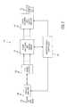
- FIG. 1is a block diagram of an amplifier module 100 constructed according to one embodiment of the present invention.
- the RF input signal 102may be provided to the amplifier module 100 from an antenna, from a transmission line, or from any other suitable electronic circuitry.
- the RF signal 102is received by a variable amplifier 104 and then forwarded to input signal splitter circuitry 106 that divides the input signal into separate signals directed to a number of available ports capable of accepting power amplifiers.
- the divided input signalis then routed to the power amplifiers and sensor circuit 108 that contains the plurality of ports into which power amplifiers may be inserted.
- the sensor circuit 108generates a control signal that is routed to a microprocessor controller 114 when power amplifiers are inserted or removed.
- the amplified output signal of each power amplifieris then forwarded to a signal combiner and output circuitry 110 that combines the signals from the power amplifiers creating a summed output signal 112 .
- the controller 114is also coupled to the output circuitry 110 and routes the summed output signal 112 through the appropriate output circuitry 110 according to the sensed occupancy level of power amplifiers within the amplifier module 100 as indicated by the control signal received from the sensor circuit 108 .
- the routerincludes a controller with various inputs and outputs and associated circuitry.
- the amplification applied to the RF input signal 102 by the variable amplifier 104is also controlled by the controller 114 .
- the amplification levelis dependent upon the number of power amplifiers detected by the controller 114 and will be discussed in more detail below.
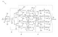
- FIG. 2depicts an amplifier module with various aspects of the invention, that contains four ports 200 - 1 , 200 - 2 , 200 - 3 , 200 - 4 , each of which is capable of accepting a power amplifier 202 .
- An amplifier module 100 according to the present inventionis not limited to having four power amplifiers. A system capable of handling fewer power amplifiers or many more may be realized in accordance with the present invention. The description of the embodiment herein is directed to a system with four power amplifier ports for illustrative purposes only to explain the various aspects of the present invention.
- the input RF signal 102is fed into the variable amplifier 104 .
- a connection between the variable amplifier 104 and the microprocessor controller 114is depicted in FIG. 2 as VA.
- FIG. 3depicts the controller 114 with connections for VA and sensor circuit nodes 1 , 2 , 3 , and 4 and switching circuit nodes A, B, C, and D which will be discussed in more detail below.
- the output of the variable amplifier 104is divided by an input signal splitter 106 and the signals are routed to four ports 200 - 1 , 200 - 2 , 200 - 3 , 200 - 4 present within the amplifier module 100 .
- the input signal splitter 106is comprised of three Wilkinson splitter networks 204 .
- Other acceptable methods for splitting the input signalmay also be used.
- the operation and method for building Wilkinson splitter networksis well known in the art and is described in “An N-Way Hybrid Power Divider” by E. J. Wilkinson, IRE Transactions on Microwave Theory and Techniques , Vol. MTT-8, No. 1, January 1960.
- the outputs of the final stage of Wilkinson splitter networks 204are coupled with the input side of the power amplifier ports 200 - 1 , 200 - 2 . 200 - 3 , 200 - 4 .
- a port 200does not contain a power amplifier 202 , then the portion of the original RF input signal 102 routed to that port is essentially lost. This phenomenon is known as “split loss.” In the preferred embodiment, which contains four ports, if a power amplifier is inserted into only one port, then three-fourths of the original RF input signal 102 will be lost. If two ports contain power amplifiers, then one-half of the original RF input signal will be lost, and so on. However, if all four ports contain a power amplifier, then little or no portion of the original input signal will be lost.
- the variable power amplifier 104compensates for any “split losses” by amplifying the RF input signal 102 to ensure the full signal strength of the original RF input signal is received by each power amplifier 200 .
- the number of amplifiers being utilizedis monitored. Using a sensor circuit, the controller 114 determines the number of power amplifiers 202 inserted within the ports 200 . As the number of power amplifiers 202 inserted within ports 200 increases, the controller 114 decreases the amplification level of the variable amplifier 104 using the control line VA. If the number of power amplifiers 202 decreases, then the controller 114 will generally increase the amplification level of the variable amplifier 104 accordingly.
- variable amplifier 104will need to amplify the original RF input signal 102 to compensate for a 6 decibel (dB) loss in the RF input signal 102 if only one power amplifier is inserted.
- dBdecibel
- a 3 dB loss in the RF input signal 102must be compensated for if two power amplifiers are inserted. If three power amplifiers are inserted, then the variable amplifier 104 must compensate for a 1.23 dB input signal loss.
- a 0 dB losswill occur if all ports 200 are occupied by power amplifiers 202 . In such an occasion, the variable amplifier generally need not amplify the RF input signal 102 .
- each port 200 and, specifically, the output of the amplifier 202 associated with the portis coupled via a section of transmission line 206 to a signal combiner 208 .
- a capacitor 210may be inserted between the output of each port 200 and the combiner 208 in order to remove any DC components from the amplified signal transmitted from the power amplifier.
- the transmission line section 206has the following line characteristics: an impedance of 50 ohms, and a length of ⁇ /2, where ⁇ is defined as the propagating wavelength of the respective RF input signal 102 .
- the embodiment depicted in FIG. 2also has an insert detection circuit 212 coupled to the output of each port 200 for determining which ports are occupied with amplifiers, in accordance with one aspect of the present invention.
- the insert detection circuit 212 in the embodimentis comprised of an inductor 214 coupled through a resistor 216 to a voltage source 218 .
- the controller 114is coupled to the insert detection circuits 212 at the sensor circuit nodes identified as 1 , 2 , 3 and 4 in FIG. 2 .
- a power amplifieris inserted into a port 200 , such as the top-most power amplifier port 200 - 1 , a voltage is generated at node 1 at the detection circuit 212 . This voltage is in the form of a control signal that is detected by the controller 114 .
- the controller 114determines that a power amplifier 202 has been inserted into the port and the port 200 - 1 is now occupied. Similarly, if a power amplifier 202 is inserted into the second port 200 - 2 , a voltage control signal is generated at node 2 of the insert detection circuit 212 , and the controller 114 determines that a second amplifier has been inserted in that respective port. The same occurs at nodes 3 and 4 if power amplifiers 202 are inserted into ports 200 - 3 or 200 - 4 .
- any power amplifier 202is removed from any one of ports 200 - 1 , 200 - 2 , 200 - 3 or 200 - 4 , then the voltage at the corresponding node 1 , 2 , 3 or 4 in the insert detection circuits 212 drops.
- the controller 114detects this drop in voltage at the appropriate node and then determines that fewer ports 200 are occupied by power amplifiers.
- insert detection circuitry 212as described above may be fed into digital circuit components. This digital circuitry may then produce a single control signal indicating the number of ports 200 occupied by power amplifiers 202 .
- the output signals from the various amplifiersare coupled to a combiner 208 , and the output of signal combiner 208 is coupled with a plurality of output lines 220 - 1 , 220 - 2 , 220 - 3 , 220 - 4 .
- each of the output lineshas different electrical line characteristics.
- the signal combiner 208receives the amplified signal created by each power amplifier 202 inserted in ports 200 and adds these signals together to create a summed output signal.
- the controllerwill direct the summed output signal of the combiner to a specific path or paths.
- the present inventionselects the output characteristics of the output signal based on the existence of amplifiers in specific ports.
- the controller 114routes the summed output signal to one of the output lines 220 coupled to the combiner 208 as is discussed below.
- the first transmission line segments 222have a length ⁇ /4 and impedances of 50, 35.35, 28.88 and 25 ohms, respectively. From the combiner, the segments 222 terminate at notes A, B., C, or D.
- Second transmission line segments 224 of length ⁇ /4 and an impedance of 50 ohms,are also coupled to the nodes A, B, C, and D.
- a grounding switch 226is coupled between a ground contact and the nodes connecting the two transmission line segments.
- the grounding switches 226are of the single-pull single-throw type (SPST); however, a variety of different switch types and/or additional transmission line segments may be used to accomplish the function of creating conditions of high and low impedance, as discussed below.
- SPSTsingle-pull single-throw type
- the first transmission line segment 222 in each output line 220is used to modify the electrical line characteristics of the respective output lines 220 .
- the impedance of transmission line segment 222is varied between each of the different output lines 220 .
- the impedance value of each transmission line segment 222 - 1 , 222 - 2 , 222 - 3 and 222 - 4is selected so that the effective impedance presented at nodes A, B, C, and D shown in FIG. 2 is transformed to generally match the impedance of the second output transmission line segments 224 , which is 50 ohms.
- the impedance values for transmission line segments 222 - 1 , 222 - 2 , 222 - 3 and 222 - 4are selected as one of multiple geometric means between the 50 ohm impedance value of the second output transmission line segment 224 and the various parallel impedance combinations of the number of ports 200 which contain power amplifiers. Depending on the number of amplifiers used, the parallel impedance of the amplifier ports will vary.
- the effective impedance presented to the input of combiner 208is 50 ohms. Therefore, to transform this impedance value to match the 50 ohm impedance of the second output transmission line segment 224 at a node (A, B, C, D) the first output transmission line segment 222 must have an impedance value which is the geometric mean of the 50 ohm impedance at the combiner input and the 50 ohm impedance of segment 224 , i.e., 50 ohms. This corresponds specifically to segment 222 and node A.
- the impedance presented to the input of the combiner 208is the parallel combination of 50 ohms and 50 ohms, i.e., 25 ohms.
- the impedance value of the output transmission line segment 222is then selected as the geometric mean between 25 and 50 ohms, which is approximately 35.35 ohms. This corresponds to segment 222 - 2 and node B.
- the combined parallel impedance at the input to combiner 208is 16.67 ohms, resulting in a value of 28.88 ohms selected as the impedance for output transmission line segment 222 - 3 and node C. If four power amplifiers are inserted into ports 200 , then the impedance value for output transmission line segment 222 - 4 associated with node D is 25 ohms.
- additional output linescan be coupled to the combiner 208 and the necessary impedance values for the first transmission line section 222 calculated according to the method and principles described above.
- the controller 114monitors the voltages at nodes 1 , 2 , 3 and 4 shown in FIG. 2 in order to determine whether a power amplifier has been inserted into one or more of the ports 200 . Based upon the number of power amplifiers detected, the controller 114 sets the grounding switches 226 located at switching circuit nodes A, B, C and D to the appropriate positions as will be described in more detail below.
- adaptive power amplifier module 100operates as follows. For example, assuming a single power amplifier is inserted into port 200 - 1 , the impedance at the input to the combiner 208 is 50 ohms. Using the sensor circuitry 212 , the controller 114 detects a voltage control signal at sensor node 1 , indicating a single power amplifier is present. No control signals are sensed at the other nodes. With a 50 ohm impedance at the combiner, it is desirable to have the output of the combiner routed to line segment 222 - 1 . This will yield an effective impedance at node A of 50 ohms.
- the controller 114closes the grounding switches 226 located at nodes B, C and D. Closing the switches grounds the nodes and causes the associated ⁇ /4 lines 222 - 2 , 222 - 3 and 222 - 4 and 224 coupled to these switches to effectively become deactivated. At a ⁇ /4 away from the grounded nodes, they are transformed into open circuits (i.e., high impedance) both at the output of combiner 208 and at the output 228 of the power amplifier module. On the other hand, the controller activates output transmission line segment 222 - 1 by causing the switch 226 at node A to be opened, or remain open. Therefore, the summed output signal from the combiner 208 will propagate through the 50 ohm, ⁇ /4 output transmission line segment 222 - 1 to be output at the power amplifier module output 228 .
- power amplifiersare inserted into ports 200 - 1 and 200 - 2 . Their combined impedance at the combiner 208 is 25 ohms.
- the controller 114would detect voltage control signals at sensor nodes 1 and 2 as shown in FIG. 2 indicating two power amplifiers are present as 200 - 1 , 200 - 2 .
- the desirable transmission line segmentis then 222 - 2 which is reflective of a geometric mean of 25 ohms and 50 ohms.
- the controller 114then causes the grounding switches 226 at nodes A, C, and D to be closed while the switch 226 at node B would be opened.
- the closed switchescause the ⁇ /4 lines 222 - 1 , 222 - 3 , 222 - 4 , and 224 associated with the nodes A, C and D to be deactivated and transformed into open circuits (i.e., high impedance) both at the output of the combiner 208 and at the power amplifier module output 228 .
- the summed output signal from combiner 208will then propagate from the output of the combiner 208 through the activated output transmission line segment 222 - 2 which has an impedance of 35.35 ohms.
- the 25-ohm impedance that was presented to this path at the combiner 208is transformed via the 35.35-ohm, ⁇ /4 line 222 - 2 to an impedance of 50 ohms at node B.
- the impedanceremains 50 ohms as it transitions through the 50-ohm, ⁇ /4 transmission line segment 224 to the output of the power amplifier module 228 .
- the same basic operationoccurs when three or four power amplifiers are inserted into ports 200 .
- the appropriate signal path when three power amplifiers are insertedis through node C and line segment 220 - 3
- the appropriate signal path when four power amplifiers are insertedis through node D and line segment 220 - 4 . Selecting the correct path ensures that the impedance from the combiner 208 to the output 228 is effectively transformed to approximately 50 ohms.
- a power amplifier system as described abovegenerally requires the use of only one switch per output line. Therefore, the total number of switches required by the system is greatly reduced. Furthermore, since the output lines are activated or deactivated by connecting the output lines to ground via the switches, the summed output signal from the combiner 208 is never required to propagate through a switch. Therefore, the switching operation of the present invention reduces the undesirable signal loss and reliability concerns that exist when multiple switches are used.
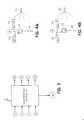
- FIGS. 4A and 4Billustrate additional embodiments of the invention, wherein additional transmission line segments are utilized with switches 226 to achieve a desired selection of an output transmission line segment.
- FIGS. 4A and 4Billustrate alternative embodiments of the invention for one of the nodes, Node A. It will be readily understood that similar alternative embodiments may be utilized for the other nodes, as well, or any number of nodes utilized in accomplishing the present invention.
- FIG. 4Autilizing switch 226 , it physically may not be able to achieve the desired closed circuit/low impedance, or open circuit/high impedance characteristics at the node. Therefore, an alternative embodiment is illustrated in FIG. 4A, and an additional transmission line segment 230 may be utilized.
- the effect on the node A from the closing of switch 226will be an opposite effect from the effect of the embodiment as illustrated in FIG. 2 . That will then also lead to an opposite effect at a distance ⁇ /4 from node A. Therefore, in order to activate the ⁇ /4 line 222 - 1 , rather than leaving the switch 222 open, the switch is closed.
- the closed switchthen translates into a high impedance at node A, but an effective low impedance at both the output of the combiner 208 and at the output 228 of the power amplifier module.
- node Ais the chosen path for the output, to deactivate the other lines, the switches are left open, translating into a low impedance at each of the respective nodes, and then a high impedance at the output of combiner 208 for each of the lines. Therefore, in the example discussed above wherein one power amplifier is present, the switch 226 associated with node A is closed, wherein the other switches remain open. Similar selective closing and opening of switches 226 may be utilized to select other nodes for the output of the combiner 208 .
- FIG. 4Billustrates still another alternative embodiment which would effectively operate similarly to the embodiment illustrated in FIG. 2 .
- an additional transmission line segment 232is utilized in combination with switch 226 to physically achieve a desired circuit.
- Transmission line segment 232is, however, ⁇ /2 in length, and therefore, the condition at the switch 226 is realized directly at the node, such as node A. That is, as discussed with respect to the embodiment illustrated in FIG. 2, the closing of switch 226 will deactivate a particular output line and node, wherein leaving the switch open will select a particular output line and node for routing the output of the combiner 208 .
- any port 200 that does not contain a power amplifieris terminated as an open-circuit impedance by operation of a switch 226 or switch/line segment combination.
- This impedanceis transformed, via the 50-ohm, ⁇ /2 segment of transmission line 206 , to the combiner 208 as an open circuit.
- This open circuit conditionwill have no impact on the overall impedance presented to the combiner 208 until a power amplifier is coupled. Therefore, amplifier modules with large numbers of unoccupied ports may be installed to accommodate for future growth. A new amplifier may be added at anytime, and the adaptive power amplifier module 100 will automatically adjust its operation, as described above, to ensure efficient operation.
- the selection of the appropriate output line 220 - 1 , 220 - 2 , 220 - 3 or 220 - 4 by the controller 114is not affected by which particular ports 200 contain power amplifiers.
- the controller 114needs to know that ports are occupied by power amplifiers; however, knowledge about which ports are occupied is irrelevant. Therefore, this system does not require power amplifiers to be installed in any particular one of ports 200 in any particular order.
- a power amplifiercan be installed in any port 200 of the power amplifier module 100 and create identical performance.
- a further feature of the preferred embodimentis that the switches 226 at nodes A, B, C and D may be “hot switched.” That is, power amplifiers can be inserted into any one of the ports 200 without having to power down the RF input signal 102 .
- the typical lifetime of these switches when hot switching is usedis limited to several operations. If the RF input 102 to the module 100 is powered down for a few milliseconds during insertion of a power amplifier (to power levels of less than 25 dBm), the lifetime of these switches may be several million operations. Typically, these switches will see no more than 10-20 operations during their lifetime.
- the adaptive power amplifier system described hereinmay be implemented to operate in a wide variety of frequency bands. Examples of the frequencies in which the preferred embodiment may be operated include cellular, the European 1800 MHz Digital Communication System (DCS), Personal Communication System (PCS), Universal Mobil Telecommunications System (UMTS), and Multichannel Multipoint Distribution System (MMDS) frequencies.
- DCSDigital Communication System
- PCSPersonal Communication System
- UMTSUniversal Mobil Telecommunications System
- MMDSMultichannel Multipoint Distribution System
Landscapes
- Engineering & Computer Science (AREA)
- Power Engineering (AREA)
- Amplifiers (AREA)
Abstract
Description
Claims (45)
Priority Applications (3)
| Application Number | Priority Date | Filing Date | Title |
|---|---|---|---|
| US10/090,857US6744312B2 (en) | 2001-03-06 | 2002-03-05 | Adaptive power amplifier system |
| AU2002252205AAU2002252205A1 (en) | 2001-03-06 | 2002-03-06 | Adaptive power amplifier system |
| PCT/US2002/006789WO2002071605A2 (en) | 2001-03-06 | 2002-03-06 | Adaptive power amplifier system |
Applications Claiming Priority (2)
| Application Number | Priority Date | Filing Date | Title |
|---|---|---|---|
| US27374601P | 2001-03-06 | 2001-03-06 | |
| US10/090,857US6744312B2 (en) | 2001-03-06 | 2002-03-05 | Adaptive power amplifier system |
Publications (2)
| Publication Number | Publication Date |
|---|---|
| US20020125944A1 US20020125944A1 (en) | 2002-09-12 |
| US6744312B2true US6744312B2 (en) | 2004-06-01 |
Family
ID=26782716
Family Applications (1)
| Application Number | Title | Priority Date | Filing Date |
|---|---|---|---|
| US10/090,857Expired - LifetimeUS6744312B2 (en) | 2001-03-06 | 2002-03-05 | Adaptive power amplifier system |
Country Status (3)
| Country | Link |
|---|---|
| US (1) | US6744312B2 (en) |
| AU (1) | AU2002252205A1 (en) |
| WO (1) | WO2002071605A2 (en) |
Cited By (8)
| Publication number | Priority date | Publication date | Assignee | Title |
|---|---|---|---|---|
| US20050110594A1 (en)* | 2003-11-21 | 2005-05-26 | Culliton Brian E. | Non-switching adaptable 4-way power splitter/combiner |
| US20050156671A1 (en)* | 2004-01-20 | 2005-07-21 | Shanjani Payman H. | Method and apparatus for compensating and improving efficiency in a variable power amplifier |
| US20060192672A1 (en)* | 2004-10-26 | 2006-08-31 | Gidge Brett D | Power line communications device and method |
| US20070118776A1 (en)* | 2005-11-22 | 2007-05-24 | Mitsubishi Electric Corporation | Power amplifier |
| US8577306B2 (en)* | 2009-03-03 | 2013-11-05 | Broadcom Corporation | Wireless communications chip with multi-port distributed antenna |
| US9344138B2 (en) | 2012-10-22 | 2016-05-17 | Emhiser Research, Inc. | Method and system for providing improved high power RF splitter/combiner |
| US9871530B1 (en) | 2016-12-11 | 2018-01-16 | John Howard La Grou | Multi-path analog-to-digital and digital-to-analog conversion of PDM signals |
| US10256782B2 (en) | 2017-04-25 | 2019-04-09 | John Howard La Grou | Multi-path power amplifier |
Families Citing this family (2)
| Publication number | Priority date | Publication date | Assignee | Title |
|---|---|---|---|---|
| US10742176B2 (en)* | 2017-11-14 | 2020-08-11 | Mediatek Singapore Pte. Ltd. | Programmable power combiner and splitter |
| US10763791B2 (en)* | 2018-12-21 | 2020-09-01 | Motorola Solutions, Inc. | Selective linearization of scalable fault tolerant frequency agile transmitters |
Citations (13)
| Publication number | Priority date | Publication date | Assignee | Title |
|---|---|---|---|---|
| US4315222A (en) | 1980-03-06 | 1982-02-09 | Bell Telephone Laboratories, Incorporated | Power combiner arrangement for microwave amplifiers |
| US4755769A (en)* | 1987-05-20 | 1988-07-05 | General Electric Company | Composite amplifier with efficient power reduction |
| US4780685A (en)* | 1987-03-19 | 1988-10-25 | General Electric Company | Composite power amplifier with redundancy |
| US5206604A (en) | 1991-12-20 | 1993-04-27 | Harris Corporation | Broadband high power amplifier |
| US5543751A (en)* | 1995-07-21 | 1996-08-06 | Motorola, Inc. | Power combiner for use in a radio frequency system and a method of constructing a power combiner |
| US5561395A (en) | 1995-01-27 | 1996-10-01 | Motorola, Inc. | Method and apparatus for self-adjusting a multistage radio frequency power amplifier |
| US5786727A (en) | 1996-10-15 | 1998-07-28 | Motorola, Inc. | Multi-stage high efficiency linear power amplifier and method therefor |
| US5862459A (en) | 1996-08-27 | 1999-01-19 | Telefonaktiebolaget Lm Ericsson | Method of and apparatus for filtering intermodulation products in a radiocommunication system |
| US5867064A (en) | 1996-08-19 | 1999-02-02 | Motorola, Inc. | Method and apparatus for improving intermodulation in a feed-forward amplifier |
| US5872481A (en)* | 1995-12-27 | 1999-02-16 | Qualcomm Incorporated | Efficient parallel-stage power amplifier |
| US5986500A (en) | 1996-12-30 | 1999-11-16 | Samsung Electronics Co., Ltd. | Combined linear power amplifying device and method |
| US6023612A (en) | 1996-07-05 | 2000-02-08 | Thomcast Communications, Inc. | Modular transmission system and method |
| US6091715A (en) | 1997-01-02 | 2000-07-18 | Dynamic Telecommunications, Inc. | Hybrid radio transceiver for wireless networks |
Family Cites Families (5)
| Publication number | Priority date | Publication date | Assignee | Title |
|---|---|---|---|---|
| US4598252A (en)* | 1984-07-06 | 1986-07-01 | Itt Corporation | Variable gain power amplifier |
| US4965530A (en)* | 1989-09-26 | 1990-10-23 | General Electric Company | Parallelled amplifier with switched isolation resistors |
| US5974041A (en)* | 1995-12-27 | 1999-10-26 | Qualcomm Incorporated | Efficient parallel-stage power amplifier |
| KR100279490B1 (en)* | 1996-08-12 | 2001-02-01 | 김덕용 | N-way power divider/combiner |
| US5834975A (en)* | 1997-03-12 | 1998-11-10 | Rockwell Science Center, Llc | Integrated variable gain power amplifier and method |
- 2002
- 2002-03-05USUS10/090,857patent/US6744312B2/ennot_activeExpired - Lifetime
- 2002-03-06WOPCT/US2002/006789patent/WO2002071605A2/ennot_activeApplication Discontinuation
- 2002-03-06AUAU2002252205Apatent/AU2002252205A1/ennot_activeAbandoned
Patent Citations (13)
| Publication number | Priority date | Publication date | Assignee | Title |
|---|---|---|---|---|
| US4315222A (en) | 1980-03-06 | 1982-02-09 | Bell Telephone Laboratories, Incorporated | Power combiner arrangement for microwave amplifiers |
| US4780685A (en)* | 1987-03-19 | 1988-10-25 | General Electric Company | Composite power amplifier with redundancy |
| US4755769A (en)* | 1987-05-20 | 1988-07-05 | General Electric Company | Composite amplifier with efficient power reduction |
| US5206604A (en) | 1991-12-20 | 1993-04-27 | Harris Corporation | Broadband high power amplifier |
| US5561395A (en) | 1995-01-27 | 1996-10-01 | Motorola, Inc. | Method and apparatus for self-adjusting a multistage radio frequency power amplifier |
| US5543751A (en)* | 1995-07-21 | 1996-08-06 | Motorola, Inc. | Power combiner for use in a radio frequency system and a method of constructing a power combiner |
| US5872481A (en)* | 1995-12-27 | 1999-02-16 | Qualcomm Incorporated | Efficient parallel-stage power amplifier |
| US6023612A (en) | 1996-07-05 | 2000-02-08 | Thomcast Communications, Inc. | Modular transmission system and method |
| US5867064A (en) | 1996-08-19 | 1999-02-02 | Motorola, Inc. | Method and apparatus for improving intermodulation in a feed-forward amplifier |
| US5862459A (en) | 1996-08-27 | 1999-01-19 | Telefonaktiebolaget Lm Ericsson | Method of and apparatus for filtering intermodulation products in a radiocommunication system |
| US5786727A (en) | 1996-10-15 | 1998-07-28 | Motorola, Inc. | Multi-stage high efficiency linear power amplifier and method therefor |
| US5986500A (en) | 1996-12-30 | 1999-11-16 | Samsung Electronics Co., Ltd. | Combined linear power amplifying device and method |
| US6091715A (en) | 1997-01-02 | 2000-07-18 | Dynamic Telecommunications, Inc. | Hybrid radio transceiver for wireless networks |
Cited By (12)
| Publication number | Priority date | Publication date | Assignee | Title |
|---|---|---|---|---|
| US20050110594A1 (en)* | 2003-11-21 | 2005-05-26 | Culliton Brian E. | Non-switching adaptable 4-way power splitter/combiner |
| US7005942B2 (en)* | 2003-11-21 | 2006-02-28 | Anaren, Inc. | Non-switching adaptable 4-way power splitter/combiner |
| US20050156671A1 (en)* | 2004-01-20 | 2005-07-21 | Shanjani Payman H. | Method and apparatus for compensating and improving efficiency in a variable power amplifier |
| US7102444B2 (en)* | 2004-01-20 | 2006-09-05 | Anadigics, Inc. | Method and apparatus for compensating and improving efficiency in a variable power amplifier |
| US20060192672A1 (en)* | 2004-10-26 | 2006-08-31 | Gidge Brett D | Power line communications device and method |
| US7450000B2 (en)* | 2004-10-26 | 2008-11-11 | Current Technologies, Llc | Power line communications device and method |
| US20070118776A1 (en)* | 2005-11-22 | 2007-05-24 | Mitsubishi Electric Corporation | Power amplifier |
| US7953997B2 (en)* | 2005-11-22 | 2011-05-31 | Mitsubishi Electric Corporation | Power amplifier |
| US8577306B2 (en)* | 2009-03-03 | 2013-11-05 | Broadcom Corporation | Wireless communications chip with multi-port distributed antenna |
| US9344138B2 (en) | 2012-10-22 | 2016-05-17 | Emhiser Research, Inc. | Method and system for providing improved high power RF splitter/combiner |
| US9871530B1 (en) | 2016-12-11 | 2018-01-16 | John Howard La Grou | Multi-path analog-to-digital and digital-to-analog conversion of PDM signals |
| US10256782B2 (en) | 2017-04-25 | 2019-04-09 | John Howard La Grou | Multi-path power amplifier |
Also Published As
| Publication number | Publication date |
|---|---|
| WO2002071605A2 (en) | 2002-09-12 |
| US20020125944A1 (en) | 2002-09-12 |
| AU2002252205A1 (en) | 2002-09-19 |
| WO2002071605A3 (en) | 2004-02-12 |
Similar Documents
| Publication | Publication Date | Title |
|---|---|---|
| US6047199A (en) | Systems and methods for transmitting mobile radio signals | |
| US6518856B1 (en) | RF power divider/combiner circuit | |
| US5884149A (en) | Mobile station having dual band RF detector and gain control | |
| US7525396B2 (en) | System, microwave switch and method for hot standby of radio frequency power amplifier | |
| US6323742B1 (en) | RF smart combiner/splitter | |
| US6744312B2 (en) | Adaptive power amplifier system | |
| US6097266A (en) | Intelligent RF combiner | |
| JP2007116745A (en) | Power amplifier system | |
| JP4538025B2 (en) | Switchable synthesizer and integrated synthesizer using the same | |
| JP2008029018A6 (en) | Switchable synthesizer and integrated synthesizer using the same | |
| US6292677B1 (en) | Power delivery system and method of controlling the power delivery system for use in a radio frequency system | |
| KR100279490B1 (en) | N-way power divider/combiner | |
| JP2012205212A (en) | High frequency power amplification device | |
| JP5582782B2 (en) | Base station architecture using distributed duplexers | |
| US7061315B2 (en) | Auxiliary amplifier network | |
| EP3868019B1 (en) | Sequenced transmit muting for wideband power amplifiers | |
| JP3820136B2 (en) | Power amplifier parallel operation system | |
| JP3502572B2 (en) | Amplifier | |
| JP2001156509A (en) | Switching power combiner | |
| KR101691418B1 (en) | Apparatus and method for maximizing performance of peaking amplifier in doherty amplifier | |
| JP3119642B2 (en) | Unselected branch termination condition switching circuit | |
| KR100352576B1 (en) | Impedance matched switchable combiner by using variable matching section | |
| KR100983517B1 (en) | Power amplifier for improving output signal in eebts | |
| US20070135067A1 (en) | Apparatus for configuring portable communication system using multipath power amplifier | |
| WO2002023757A1 (en) | Switchable power divider |
Legal Events
| Date | Code | Title | Description |
|---|---|---|---|
| AS | Assignment | Owner name:ANDREW CORPORATION, ILLINOIS Free format text:ASSIGNMENT OF ASSIGNORS INTEREST;ASSIGNORS:WHITE, PAUL E.;KOOKER, ROBERT W.;REEL/FRAME:012671/0763 Effective date:20020221 | |
| STCF | Information on status: patent grant | Free format text:PATENTED CASE | |
| CC | Certificate of correction | ||
| FPAY | Fee payment | Year of fee payment:4 | |
| AS | Assignment | Owner name:BANK OF AMERICA, N.A., AS ADMINISTRATIVE AGENT, CA Free format text:SECURITY AGREEMENT;ASSIGNORS:COMMSCOPE, INC. OF NORTH CAROLINA;ALLEN TELECOM, LLC;ANDREW CORPORATION;REEL/FRAME:020362/0241 Effective date:20071227 Owner name:BANK OF AMERICA, N.A., AS ADMINISTRATIVE AGENT,CAL Free format text:SECURITY AGREEMENT;ASSIGNORS:COMMSCOPE, INC. OF NORTH CAROLINA;ALLEN TELECOM, LLC;ANDREW CORPORATION;REEL/FRAME:020362/0241 Effective date:20071227 | |
| AS | Assignment | Owner name:ANDREW LLC, NORTH CAROLINA Free format text:CHANGE OF NAME;ASSIGNOR:ANDREW CORPORATION;REEL/FRAME:021805/0044 Effective date:20080827 | |
| AS | Assignment | Owner name:ALLEN TELECOM LLC, NORTH CAROLINA Free format text:PATENT RELEASE;ASSIGNOR:BANK OF AMERICA, N.A., AS ADMINISTRATIVE AGENT;REEL/FRAME:026039/0005 Effective date:20110114 Owner name:COMMSCOPE, INC. OF NORTH CAROLINA, NORTH CAROLINA Free format text:PATENT RELEASE;ASSIGNOR:BANK OF AMERICA, N.A., AS ADMINISTRATIVE AGENT;REEL/FRAME:026039/0005 Effective date:20110114 Owner name:ANDREW LLC (F/K/A ANDREW CORPORATION), NORTH CAROL Free format text:PATENT RELEASE;ASSIGNOR:BANK OF AMERICA, N.A., AS ADMINISTRATIVE AGENT;REEL/FRAME:026039/0005 Effective date:20110114 | |
| AS | Assignment | Owner name:JPMORGAN CHASE BANK, N.A., AS COLLATERAL AGENT, NE Free format text:SECURITY AGREEMENT;ASSIGNORS:ALLEN TELECOM LLC, A DELAWARE LLC;ANDREW LLC, A DELAWARE LLC;COMMSCOPE, INC. OF NORTH CAROLINA, A NORTH CAROLINA CORPORATION;REEL/FRAME:026276/0363 Effective date:20110114 | |
| AS | Assignment | Owner name:JPMORGAN CHASE BANK, N.A., AS COLLATERAL AGENT, NE Free format text:SECURITY AGREEMENT;ASSIGNORS:ALLEN TELECOM LLC, A DELAWARE LLC;ANDREW LLC, A DELAWARE LLC;COMMSCOPE, INC OF NORTH CAROLINA, A NORTH CAROLINA CORPORATION;REEL/FRAME:026272/0543 Effective date:20110114 | |
| FPAY | Fee payment | Year of fee payment:8 | |
| AS | Assignment | Owner name:COMMSCOPE TECHNOLOGIES LLC, NORTH CAROLINA Free format text:CHANGE OF NAME;ASSIGNOR:ANDREW LLC;REEL/FRAME:035226/0949 Effective date:20150301 | |
| AS | Assignment | Owner name:WILMINGTON TRUST, NATIONAL ASSOCIATION, AS COLLATERAL AGENT, CONNECTICUT Free format text:SECURITY INTEREST;ASSIGNORS:ALLEN TELECOM LLC;COMMSCOPE TECHNOLOGIES LLC;COMMSCOPE, INC. OF NORTH CAROLINA;AND OTHERS;REEL/FRAME:036201/0283 Effective date:20150611 Owner name:WILMINGTON TRUST, NATIONAL ASSOCIATION, AS COLLATE Free format text:SECURITY INTEREST;ASSIGNORS:ALLEN TELECOM LLC;COMMSCOPE TECHNOLOGIES LLC;COMMSCOPE, INC. OF NORTH CAROLINA;AND OTHERS;REEL/FRAME:036201/0283 Effective date:20150611 | |
| FPAY | Fee payment | Year of fee payment:12 | |
| AS | Assignment | Owner name:COMMSCOPE, INC. OF NORTH CAROLINA, NORTH CAROLINA Free format text:RELEASE OF SECURITY INTEREST PATENTS (RELEASES RF 036201/0283);ASSIGNOR:WILMINGTON TRUST, NATIONAL ASSOCIATION;REEL/FRAME:042126/0434 Effective date:20170317 Owner name:COMMSCOPE TECHNOLOGIES LLC, NORTH CAROLINA Free format text:RELEASE OF SECURITY INTEREST PATENTS (RELEASES RF 036201/0283);ASSIGNOR:WILMINGTON TRUST, NATIONAL ASSOCIATION;REEL/FRAME:042126/0434 Effective date:20170317 Owner name:REDWOOD SYSTEMS, INC., NORTH CAROLINA Free format text:RELEASE OF SECURITY INTEREST PATENTS (RELEASES RF 036201/0283);ASSIGNOR:WILMINGTON TRUST, NATIONAL ASSOCIATION;REEL/FRAME:042126/0434 Effective date:20170317 Owner name:ALLEN TELECOM LLC, NORTH CAROLINA Free format text:RELEASE OF SECURITY INTEREST PATENTS (RELEASES RF 036201/0283);ASSIGNOR:WILMINGTON TRUST, NATIONAL ASSOCIATION;REEL/FRAME:042126/0434 Effective date:20170317 | |
| AS | Assignment | Owner name:COMMSCOPE, INC. OF NORTH CAROLINA, NORTH CAROLINA Free format text:RELEASE BY SECURED PARTY;ASSIGNOR:JPMORGAN CHASE BANK, N.A.;REEL/FRAME:048840/0001 Effective date:20190404 Owner name:ANDREW LLC, NORTH CAROLINA Free format text:RELEASE BY SECURED PARTY;ASSIGNOR:JPMORGAN CHASE BANK, N.A.;REEL/FRAME:048840/0001 Effective date:20190404 Owner name:COMMSCOPE TECHNOLOGIES LLC, NORTH CAROLINA Free format text:RELEASE BY SECURED PARTY;ASSIGNOR:JPMORGAN CHASE BANK, N.A.;REEL/FRAME:048840/0001 Effective date:20190404 Owner name:REDWOOD SYSTEMS, INC., NORTH CAROLINA Free format text:RELEASE BY SECURED PARTY;ASSIGNOR:JPMORGAN CHASE BANK, N.A.;REEL/FRAME:048840/0001 Effective date:20190404 Owner name:ALLEN TELECOM LLC, ILLINOIS Free format text:RELEASE BY SECURED PARTY;ASSIGNOR:JPMORGAN CHASE BANK, N.A.;REEL/FRAME:048840/0001 Effective date:20190404 Owner name:ALLEN TELECOM LLC, ILLINOIS Free format text:RELEASE BY SECURED PARTY;ASSIGNOR:JPMORGAN CHASE BANK, N.A.;REEL/FRAME:049260/0001 Effective date:20190404 Owner name:COMMSCOPE, INC. OF NORTH CAROLINA, NORTH CAROLINA Free format text:RELEASE BY SECURED PARTY;ASSIGNOR:JPMORGAN CHASE BANK, N.A.;REEL/FRAME:049260/0001 Effective date:20190404 Owner name:REDWOOD SYSTEMS, INC., NORTH CAROLINA Free format text:RELEASE BY SECURED PARTY;ASSIGNOR:JPMORGAN CHASE BANK, N.A.;REEL/FRAME:049260/0001 Effective date:20190404 Owner name:COMMSCOPE TECHNOLOGIES LLC, NORTH CAROLINA Free format text:RELEASE BY SECURED PARTY;ASSIGNOR:JPMORGAN CHASE BANK, N.A.;REEL/FRAME:049260/0001 Effective date:20190404 Owner name:ANDREW LLC, NORTH CAROLINA Free format text:RELEASE BY SECURED PARTY;ASSIGNOR:JPMORGAN CHASE BANK, N.A.;REEL/FRAME:049260/0001 Effective date:20190404 | |
| AS | Assignment | Owner name:WILMINGTON TRUST, NATIONAL ASSOCIATION, AS COLLATE Free format text:PATENT SECURITY AGREEMENT;ASSIGNOR:COMMSCOPE TECHNOLOGIES LLC;REEL/FRAME:049892/0051 Effective date:20190404 Owner name:JPMORGAN CHASE BANK, N.A., NEW YORK Free format text:ABL SECURITY AGREEMENT;ASSIGNORS:COMMSCOPE, INC. OF NORTH CAROLINA;COMMSCOPE TECHNOLOGIES LLC;ARRIS ENTERPRISES LLC;AND OTHERS;REEL/FRAME:049892/0396 Effective date:20190404 Owner name:JPMORGAN CHASE BANK, N.A., NEW YORK Free format text:TERM LOAN SECURITY AGREEMENT;ASSIGNORS:COMMSCOPE, INC. OF NORTH CAROLINA;COMMSCOPE TECHNOLOGIES LLC;ARRIS ENTERPRISES LLC;AND OTHERS;REEL/FRAME:049905/0504 Effective date:20190404 Owner name:WILMINGTON TRUST, NATIONAL ASSOCIATION, AS COLLATERAL AGENT, CONNECTICUT Free format text:PATENT SECURITY AGREEMENT;ASSIGNOR:COMMSCOPE TECHNOLOGIES LLC;REEL/FRAME:049892/0051 Effective date:20190404 | |
| AS | Assignment | Owner name:WILMINGTON TRUST, DELAWARE Free format text:SECURITY INTEREST;ASSIGNORS:ARRIS SOLUTIONS, INC.;ARRIS ENTERPRISES LLC;COMMSCOPE TECHNOLOGIES LLC;AND OTHERS;REEL/FRAME:060752/0001 Effective date:20211115 | |
| AS | Assignment | Owner name:RUCKUS WIRELESS, LLC (F/K/A RUCKUS WIRELESS, INC.), NORTH CAROLINA Free format text:RELEASE OF SECURITY INTEREST AT REEL/FRAME 049905/0504;ASSIGNOR:JPMORGAN CHASE BANK, N.A., AS COLLATERAL AGENT;REEL/FRAME:071477/0255 Effective date:20241217 Owner name:COMMSCOPE TECHNOLOGIES LLC, NORTH CAROLINA Free format text:RELEASE OF SECURITY INTEREST AT REEL/FRAME 049905/0504;ASSIGNOR:JPMORGAN CHASE BANK, N.A., AS COLLATERAL AGENT;REEL/FRAME:071477/0255 Effective date:20241217 Owner name:COMMSCOPE, INC. OF NORTH CAROLINA, NORTH CAROLINA Free format text:RELEASE OF SECURITY INTEREST AT REEL/FRAME 049905/0504;ASSIGNOR:JPMORGAN CHASE BANK, N.A., AS COLLATERAL AGENT;REEL/FRAME:071477/0255 Effective date:20241217 Owner name:ARRIS SOLUTIONS, INC., NORTH CAROLINA Free format text:RELEASE OF SECURITY INTEREST AT REEL/FRAME 049905/0504;ASSIGNOR:JPMORGAN CHASE BANK, N.A., AS COLLATERAL AGENT;REEL/FRAME:071477/0255 Effective date:20241217 Owner name:ARRIS TECHNOLOGY, INC., NORTH CAROLINA Free format text:RELEASE OF SECURITY INTEREST AT REEL/FRAME 049905/0504;ASSIGNOR:JPMORGAN CHASE BANK, N.A., AS COLLATERAL AGENT;REEL/FRAME:071477/0255 Effective date:20241217 Owner name:ARRIS ENTERPRISES LLC (F/K/A ARRIS ENTERPRISES, INC.), NORTH CAROLINA Free format text:RELEASE OF SECURITY INTEREST AT REEL/FRAME 049905/0504;ASSIGNOR:JPMORGAN CHASE BANK, N.A., AS COLLATERAL AGENT;REEL/FRAME:071477/0255 Effective date:20241217 |