US6744138B2 - RuSixOy-containing barrier layers for high-k dielectrics - Google Patents
RuSixOy-containing barrier layers for high-k dielectricsDownload PDFInfo
- Publication number
- US6744138B2 US6744138B2US10/136,771US13677102AUS6744138B2US 6744138 B2US6744138 B2US 6744138B2US 13677102 AUS13677102 AUS 13677102AUS 6744138 B2US6744138 B2US 6744138B2
- Authority
- US
- United States
- Prior art keywords
- rusi
- diffusion barrier
- barrier layer
- silicon
- layer
- Prior art date
- Legal status (The legal status is an assumption and is not a legal conclusion. Google has not performed a legal analysis and makes no representation as to the accuracy of the status listed.)
- Expired - Lifetime
Links
- 230000004888barrier functionEffects0.000titleclaimsabstractdescription126
- 239000003989dielectric materialSubstances0.000titledescription8
- 238000009792diffusion processMethods0.000claimsabstractdescription110
- 229910052710siliconInorganic materials0.000claimsabstractdescription65
- XUIMIQQOPSSXEZ-UHFFFAOYSA-NSiliconChemical compound[Si]XUIMIQQOPSSXEZ-UHFFFAOYSA-N0.000claimsabstractdescription64
- 239000010703siliconSubstances0.000claimsabstractdescription64
- 229910052707rutheniumInorganic materials0.000claimsabstractdescription48
- 239000000758substrateSubstances0.000claimsabstractdescription40
- WOCIAKWEIIZHES-UHFFFAOYSA-Nruthenium(iv) oxideChemical compoundO=[Ru]=OWOCIAKWEIIZHES-UHFFFAOYSA-N0.000claimsabstractdescription34
- 239000004065semiconductorSubstances0.000claimsabstractdescription24
- 239000000463materialSubstances0.000claimsdescription31
- 229910052697platinumInorganic materials0.000claimsdescription14
- QXYJCZRRLLQGCR-UHFFFAOYSA-NdioxomolybdenumChemical compoundO=[Mo]=OQXYJCZRRLLQGCR-UHFFFAOYSA-N0.000claimsdescription12
- 229910052751metalInorganic materials0.000claimsdescription11
- 239000002184metalSubstances0.000claimsdescription11
- 239000004020conductorSubstances0.000claimsdescription9
- 229910052741iridiumInorganic materials0.000claimsdescription8
- HTXDPTMKBJXEOW-UHFFFAOYSA-Niridium(IV) oxideInorganic materialsO=[Ir]=OHTXDPTMKBJXEOW-UHFFFAOYSA-N0.000claimsdescription8
- 229910044991metal oxideInorganic materials0.000claimsdescription8
- 150000004706metal oxidesChemical class0.000claimsdescription8
- 229910052763palladiumInorganic materials0.000claimsdescription7
- 229910052703rhodiumInorganic materials0.000claimsdescription7
- 229910019834RhO2Inorganic materials0.000claimsdescription6
- KZYDBKYFEURFNC-UHFFFAOYSA-NdioxorhodiumChemical compoundO=[Rh]=OKZYDBKYFEURFNC-UHFFFAOYSA-N0.000claimsdescription6
- 229910052721tungstenInorganic materials0.000claimsdescription5
- XSXHWVKGUXMUQE-UHFFFAOYSA-Nosmium dioxideInorganic materialsO=[Os]=OXSXHWVKGUXMUQE-UHFFFAOYSA-N0.000claims3
- 238000000034methodMethods0.000abstractdescription70
- KJTLSVCANCCWHF-UHFFFAOYSA-NRutheniumChemical compound[Ru]KJTLSVCANCCWHF-UHFFFAOYSA-N0.000abstractdescription45
- 238000005229chemical vapour depositionMethods0.000abstractdescription43
- 238000000151depositionMethods0.000abstractdescription38
- 239000003990capacitorSubstances0.000abstractdescription33
- 229910001925ruthenium oxideInorganic materials0.000abstractdescription12
- 238000000231atomic layer depositionMethods0.000abstractdescription10
- 238000004519manufacturing processMethods0.000abstractdescription8
- 238000005240physical vapour depositionMethods0.000abstractdescription8
- 239000010410layerSubstances0.000description187
- 230000008569processEffects0.000description34
- 239000007789gasSubstances0.000description33
- 239000002243precursorSubstances0.000description31
- 230000008021depositionEffects0.000description29
- 238000006243chemical reactionMethods0.000description28
- BASFCYQUMIYNBI-UHFFFAOYSA-NplatinumChemical compound[Pt]BASFCYQUMIYNBI-UHFFFAOYSA-N0.000description24
- 239000010408filmSubstances0.000description19
- 239000002356single layerSubstances0.000description19
- QVGXLLKOCUKJST-UHFFFAOYSA-Natomic oxygenChemical compound[O]QVGXLLKOCUKJST-UHFFFAOYSA-N0.000description16
- 229910052760oxygenInorganic materials0.000description16
- 239000001301oxygenSubstances0.000description16
- 235000012431wafersNutrition0.000description14
- 210000000352storage cellAnatomy0.000description13
- 230000015572biosynthetic processEffects0.000description12
- VYPSYNLAJGMNEJ-UHFFFAOYSA-NSilicium dioxideChemical compoundO=[Si]=OVYPSYNLAJGMNEJ-UHFFFAOYSA-N0.000description10
- 230000001590oxidative effectEffects0.000description10
- 150000001875compoundsChemical class0.000description9
- XKRFYHLGVUSROY-UHFFFAOYSA-NArgonChemical compound[Ar]XKRFYHLGVUSROY-UHFFFAOYSA-N0.000description8
- GQPLMRYTRLFLPF-UHFFFAOYSA-NNitrous OxideChemical compound[O-][N+]#NGQPLMRYTRLFLPF-UHFFFAOYSA-N0.000description8
- 230000003647oxidationEffects0.000description8
- 238000007254oxidation reactionMethods0.000description8
- 238000010926purgeMethods0.000description8
- ATJFFYVFTNAWJD-UHFFFAOYSA-NTinChemical compound[Sn]ATJFFYVFTNAWJD-UHFFFAOYSA-N0.000description7
- -1for exampleChemical class0.000description7
- 239000000376reactantSubstances0.000description7
- 239000012686silicon precursorSubstances0.000description7
- 238000000137annealingMethods0.000description6
- 239000012298atmosphereSubstances0.000description6
- 239000012495reaction gasSubstances0.000description6
- 229910052786argonInorganic materials0.000description5
- 238000000429assemblyMethods0.000description5
- 230000000712assemblyEffects0.000description5
- 239000012159carrier gasSubstances0.000description5
- 229910052681coesiteInorganic materials0.000description5
- 229910052906cristobaliteInorganic materials0.000description5
- PZPGRFITIJYNEJ-UHFFFAOYSA-NdisilaneChemical compound[SiH3][SiH3]PZPGRFITIJYNEJ-UHFFFAOYSA-N0.000description5
- 150000002739metalsChemical class0.000description5
- KDLHZDBZIXYQEI-UHFFFAOYSA-NpalladiumSubstances[Pd]KDLHZDBZIXYQEI-UHFFFAOYSA-N0.000description5
- 239000010948rhodiumSubstances0.000description5
- 239000000377silicon dioxideSubstances0.000description5
- 229910052682stishoviteInorganic materials0.000description5
- 229910052905tridymiteInorganic materials0.000description5
- BLRPTPMANUNPDV-UHFFFAOYSA-NSilaneChemical compound[SiH4]BLRPTPMANUNPDV-UHFFFAOYSA-N0.000description4
- 229910052734heliumInorganic materials0.000description4
- 230000015654memoryEffects0.000description4
- 239000000203mixtureSubstances0.000description4
- 239000007800oxidant agentSubstances0.000description4
- 238000012545processingMethods0.000description4
- 239000007787solidSubstances0.000description4
- 229910007264Si2H6Inorganic materials0.000description3
- 125000004429atomChemical group0.000description3
- 230000008901benefitEffects0.000description3
- 210000004027cellAnatomy0.000description3
- 230000003247decreasing effectEffects0.000description3
- 150000001993dienesChemical class0.000description3
- 238000010790dilutionMethods0.000description3
- 239000012895dilutionSubstances0.000description3
- 239000001307heliumSubstances0.000description3
- SWQJXJOGLNCZEY-UHFFFAOYSA-Nhelium atomChemical compound[He]SWQJXJOGLNCZEY-UHFFFAOYSA-N0.000description3
- GKOZUEZYRPOHIO-UHFFFAOYSA-Niridium atomChemical compound[Ir]GKOZUEZYRPOHIO-UHFFFAOYSA-N0.000description3
- 229910000457iridium oxideInorganic materials0.000description3
- 239000007788liquidSubstances0.000description3
- 238000001465metallisationMethods0.000description3
- 229910000077silaneInorganic materials0.000description3
- 238000003860storageMethods0.000description3
- IJGRMHOSHXDMSA-UHFFFAOYSA-NAtomic nitrogenChemical compoundN#NIJGRMHOSHXDMSA-UHFFFAOYSA-N0.000description2
- CURLTUGMZLYLDI-UHFFFAOYSA-NCarbon dioxideChemical compoundO=C=OCURLTUGMZLYLDI-UHFFFAOYSA-N0.000description2
- WYURNTSHIVDZCO-UHFFFAOYSA-NTetrahydrofuranChemical compoundC1CCOC1WYURNTSHIVDZCO-UHFFFAOYSA-N0.000description2
- 229910010252TiO3Inorganic materials0.000description2
- NRTOMJZYCJJWKI-UHFFFAOYSA-NTitanium nitrideChemical compound[Ti]#NNRTOMJZYCJJWKI-UHFFFAOYSA-N0.000description2
- 229910052782aluminiumInorganic materials0.000description2
- XAGFODPZIPBFFR-UHFFFAOYSA-NaluminiumChemical compound[Al]XAGFODPZIPBFFR-UHFFFAOYSA-N0.000description2
- 230000009286beneficial effectEffects0.000description2
- 230000005669field effectEffects0.000description2
- 239000011521glassSubstances0.000description2
- 229910052746lanthanumInorganic materials0.000description2
- 238000004518low pressure chemical vapour depositionMethods0.000description2
- 238000012986modificationMethods0.000description2
- 230000004048modificationEffects0.000description2
- 229910000476molybdenum oxideInorganic materials0.000description2
- PQQKPALAQIIWST-UHFFFAOYSA-NoxomolybdenumChemical compound[Mo]=OPQQKPALAQIIWST-UHFFFAOYSA-N0.000description2
- 238000000623plasma-assisted chemical vapour depositionMethods0.000description2
- 229910003446platinum oxideInorganic materials0.000description2
- FGIUAXJPYTZDNR-UHFFFAOYSA-Npotassium nitrateChemical compound[K+].[O-][N+]([O-])=OFGIUAXJPYTZDNR-UHFFFAOYSA-N0.000description2
- MHOVAHRLVXNVSD-UHFFFAOYSA-Nrhodium atomChemical compound[Rh]MHOVAHRLVXNVSD-UHFFFAOYSA-N0.000description2
- 229910003450rhodium oxideInorganic materials0.000description2
- 150000003303rutheniumChemical class0.000description2
- 229910001927ruthenium tetroxideInorganic materials0.000description2
- 241000894007speciesSpecies0.000description2
- 238000004544sputter depositionMethods0.000description2
- 239000000126substanceSubstances0.000description2
- PBCFLUZVCVVTBY-UHFFFAOYSA-Ntantalum pentoxideInorganic materialsO=[Ta](=O)O[Ta](=O)=OPBCFLUZVCVVTBY-UHFFFAOYSA-N0.000description2
- 239000010409thin filmSubstances0.000description2
- 230000008016vaporizationEffects0.000description2
- 239000003039volatile agentSubstances0.000description2
- 229910015838BaxSr(1-x)TiO3Inorganic materials0.000description1
- MYMOFIZGZYHOMD-UHFFFAOYSA-NDioxygenChemical compoundO=OMYMOFIZGZYHOMD-UHFFFAOYSA-N0.000description1
- 229910003327LiNbO3Inorganic materials0.000description1
- 229910020294Pb(Zr,Ti)O3Inorganic materials0.000description1
- 229910003781PbTiO3Inorganic materials0.000description1
- 229910000629Rh alloyInorganic materials0.000description1
- 229910019895RuSiInorganic materials0.000description1
- 229910003818SiH2Cl2Inorganic materials0.000description1
- 229910003822SiHCl3Inorganic materials0.000description1
- 229910002370SrTiO3Inorganic materials0.000description1
- 239000003570airSubstances0.000description1
- 229910045601alloyInorganic materials0.000description1
- 239000000956alloySubstances0.000description1
- 239000003708ampulSubstances0.000description1
- 229910052785arsenicInorganic materials0.000description1
- 238000001505atmospheric-pressure chemical vapour depositionMethods0.000description1
- 238000003877atomic layer epitaxyMethods0.000description1
- 229910002113barium titanateInorganic materials0.000description1
- 239000006227byproductSubstances0.000description1
- 239000001569carbon dioxideSubstances0.000description1
- 229910002092carbon dioxideInorganic materials0.000description1
- SIGRRDAVQRKJGV-UHFFFAOYSA-Ncarbon monoxide;cyclopentane;ruthenium(1+)Chemical class[Ru+].[O+]#[C-].[O+]#[C-].[CH]1[CH][CH][CH][CH]1SIGRRDAVQRKJGV-UHFFFAOYSA-N0.000description1
- NQZFAUXPNWSLBI-UHFFFAOYSA-Ncarbon monoxide;rutheniumChemical group[Ru].[Ru].[Ru].[O+]#[C-].[O+]#[C-].[O+]#[C-].[O+]#[C-].[O+]#[C-].[O+]#[C-].[O+]#[C-].[O+]#[C-].[O+]#[C-].[O+]#[C-].[O+]#[C-].[O+]#[C-]NQZFAUXPNWSLBI-UHFFFAOYSA-N0.000description1
- 230000015556catabolic processEffects0.000description1
- 230000008859changeEffects0.000description1
- 238000007796conventional methodMethods0.000description1
- 229910052802copperInorganic materials0.000description1
- YHGGQZOFJGJAMR-UHFFFAOYSA-Ncyclopenta-1,3-diene rutheniumChemical compoundC1=CC=CC1.C1=CC=CC1.[Ru]YHGGQZOFJGJAMR-UHFFFAOYSA-N0.000description1
- 238000000354decomposition reactionMethods0.000description1
- 238000006731degradation reactionMethods0.000description1
- 230000001419dependent effectEffects0.000description1
- 238000005137deposition processMethods0.000description1
- MROCJMGDEKINLD-UHFFFAOYSA-NdichlorosilaneChemical compoundCl[SiH2]ClMROCJMGDEKINLD-UHFFFAOYSA-N0.000description1
- 229910001882dioxygenInorganic materials0.000description1
- 239000007772electrode materialSubstances0.000description1
- 238000000605extractionMethods0.000description1
- 230000006870functionEffects0.000description1
- 125000005843halogen groupChemical group0.000description1
- 238000010438heat treatmentMethods0.000description1
- 125000005842heteroatomChemical group0.000description1
- 238000011065in-situ storageMethods0.000description1
- 239000011261inert gasSubstances0.000description1
- 230000010354integrationEffects0.000description1
- 238000010884ion-beam techniqueMethods0.000description1
- 230000005012migrationEffects0.000description1
- 238000013508migrationMethods0.000description1
- 229910052754neonInorganic materials0.000description1
- GKAOGPIIYCISHV-UHFFFAOYSA-Nneon atomChemical compound[Ne]GKAOGPIIYCISHV-UHFFFAOYSA-N0.000description1
- 229910052757nitrogenInorganic materials0.000description1
- 239000012299nitrogen atmosphereSubstances0.000description1
- 239000001272nitrous oxideSubstances0.000description1
- 150000002908osmium compoundsChemical class0.000description1
- SJLOMQIUPFZJAN-UHFFFAOYSA-NoxorhodiumChemical compound[Rh]=OSJLOMQIUPFZJAN-UHFFFAOYSA-N0.000description1
- 230000035699permeabilityEffects0.000description1
- 238000005498polishingMethods0.000description1
- 229910021420polycrystalline siliconInorganic materials0.000description1
- 229920005591polysiliconPolymers0.000description1
- 239000000047productSubstances0.000description1
- 238000001552radio frequency sputter depositionMethods0.000description1
- 238000011160researchMethods0.000description1
- 229910052594sapphireInorganic materials0.000description1
- 239000010980sapphireSubstances0.000description1
- 229910021332silicideInorganic materials0.000description1
- FVBUAEGBCNSCDD-UHFFFAOYSA-Nsilicide(4-)Chemical compound[Si-4]FVBUAEGBCNSCDD-UHFFFAOYSA-N0.000description1
- 229910052990silicon hydrideInorganic materials0.000description1
- 230000003068static effectEffects0.000description1
- 229910052717sulfurInorganic materials0.000description1
- 238000006557surface reactionMethods0.000description1
- MZLGASXMSKOWSE-UHFFFAOYSA-Ntantalum nitrideChemical compound[Ta]#NMZLGASXMSKOWSE-UHFFFAOYSA-N0.000description1
- YLQBMQCUIZJEEH-UHFFFAOYSA-NtetrahydrofuranNatural productsC=1C=COC=1YLQBMQCUIZJEEH-UHFFFAOYSA-N0.000description1
- 239000010936titaniumSubstances0.000description1
- 229910052719titaniumInorganic materials0.000description1
- ZDHXKXAHOVTTAH-UHFFFAOYSA-NtrichlorosilaneChemical compoundCl[SiH](Cl)ClZDHXKXAHOVTTAH-UHFFFAOYSA-N0.000description1
- 239000005052trichlorosilaneSubstances0.000description1
- 239000010937tungstenSubstances0.000description1
- 239000012808vapor phaseSubstances0.000description1
- 238000009834vaporizationMethods0.000description1
- 229910052724xenonInorganic materials0.000description1
- FHNFHKCVQCLJFQ-UHFFFAOYSA-Nxenon atomChemical compound[Xe]FHNFHKCVQCLJFQ-UHFFFAOYSA-N0.000description1
Images


Classifications
- H—ELECTRICITY
- H01—ELECTRIC ELEMENTS
- H01L—SEMICONDUCTOR DEVICES NOT COVERED BY CLASS H10
- H01L21/00—Processes or apparatus adapted for the manufacture or treatment of semiconductor or solid state devices or of parts thereof
- H01L21/70—Manufacture or treatment of devices consisting of a plurality of solid state components formed in or on a common substrate or of parts thereof; Manufacture of integrated circuit devices or of parts thereof
- H01L21/71—Manufacture of specific parts of devices defined in group H01L21/70
- H01L21/768—Applying interconnections to be used for carrying current between separate components within a device comprising conductors and dielectrics
- H01L21/76838—Applying interconnections to be used for carrying current between separate components within a device comprising conductors and dielectrics characterised by the formation and the after-treatment of the conductors
- H01L21/76841—Barrier, adhesion or liner layers
- H01L21/76843—Barrier, adhesion or liner layers formed in openings in a dielectric
- H—ELECTRICITY
- H01—ELECTRIC ELEMENTS
- H01L—SEMICONDUCTOR DEVICES NOT COVERED BY CLASS H10
- H01L21/00—Processes or apparatus adapted for the manufacture or treatment of semiconductor or solid state devices or of parts thereof
- H01L21/02—Manufacture or treatment of semiconductor devices or of parts thereof
- H01L21/04—Manufacture or treatment of semiconductor devices or of parts thereof the devices having potential barriers, e.g. a PN junction, depletion layer or carrier concentration layer
- H01L21/18—Manufacture or treatment of semiconductor devices or of parts thereof the devices having potential barriers, e.g. a PN junction, depletion layer or carrier concentration layer the devices having semiconductor bodies comprising elements of Group IV of the Periodic Table or AIIIBV compounds with or without impurities, e.g. doping materials
- H01L21/28—Manufacture of electrodes on semiconductor bodies using processes or apparatus not provided for in groups H01L21/20 - H01L21/268
- H01L21/283—Deposition of conductive or insulating materials for electrodes conducting electric current
- H01L21/285—Deposition of conductive or insulating materials for electrodes conducting electric current from a gas or vapour, e.g. condensation
- H01L21/28506—Deposition of conductive or insulating materials for electrodes conducting electric current from a gas or vapour, e.g. condensation of conductive layers
- H01L21/28512—Deposition of conductive or insulating materials for electrodes conducting electric current from a gas or vapour, e.g. condensation of conductive layers on semiconductor bodies comprising elements of Group IV of the Periodic Table
- H01L21/28556—Deposition of conductive or insulating materials for electrodes conducting electric current from a gas or vapour, e.g. condensation of conductive layers on semiconductor bodies comprising elements of Group IV of the Periodic Table by chemical means, e.g. CVD, LPCVD, PECVD, laser CVD
- H01L21/28562—Selective deposition
- H—ELECTRICITY
- H01—ELECTRIC ELEMENTS
- H01L—SEMICONDUCTOR DEVICES NOT COVERED BY CLASS H10
- H01L21/00—Processes or apparatus adapted for the manufacture or treatment of semiconductor or solid state devices or of parts thereof
- H01L21/70—Manufacture or treatment of devices consisting of a plurality of solid state components formed in or on a common substrate or of parts thereof; Manufacture of integrated circuit devices or of parts thereof
- H01L21/71—Manufacture of specific parts of devices defined in group H01L21/70
- H01L21/768—Applying interconnections to be used for carrying current between separate components within a device comprising conductors and dielectrics
- H01L21/76838—Applying interconnections to be used for carrying current between separate components within a device comprising conductors and dielectrics characterised by the formation and the after-treatment of the conductors
- H01L21/76841—Barrier, adhesion or liner layers
- H01L21/76853—Barrier, adhesion or liner layers characterized by particular after-treatment steps
- H01L21/76855—After-treatment introducing at least one additional element into the layer
- H01L21/76856—After-treatment introducing at least one additional element into the layer by treatment in plasmas or gaseous environments, e.g. nitriding a refractory metal liner
- H—ELECTRICITY
- H01—ELECTRIC ELEMENTS
- H01L—SEMICONDUCTOR DEVICES NOT COVERED BY CLASS H10
- H01L23/00—Details of semiconductor or other solid state devices
- H01L23/48—Arrangements for conducting electric current to or from the solid state body in operation, e.g. leads, terminal arrangements ; Selection of materials therefor
- H01L23/482—Arrangements for conducting electric current to or from the solid state body in operation, e.g. leads, terminal arrangements ; Selection of materials therefor consisting of lead-in layers inseparably applied to the semiconductor body (electrodes)
- H01L23/485—Arrangements for conducting electric current to or from the solid state body in operation, e.g. leads, terminal arrangements ; Selection of materials therefor consisting of lead-in layers inseparably applied to the semiconductor body (electrodes) consisting of layered constructions comprising conductive layers and insulating layers, e.g. planar contacts
- H—ELECTRICITY
- H01—ELECTRIC ELEMENTS
- H01L—SEMICONDUCTOR DEVICES NOT COVERED BY CLASS H10
- H01L23/00—Details of semiconductor or other solid state devices
- H01L23/52—Arrangements for conducting electric current within the device in operation from one component to another, i.e. interconnections, e.g. wires, lead frames
- H01L23/522—Arrangements for conducting electric current within the device in operation from one component to another, i.e. interconnections, e.g. wires, lead frames including external interconnections consisting of a multilayer structure of conductive and insulating layers inseparably formed on the semiconductor body
- H01L23/5222—Capacitive arrangements or effects of, or between wiring layers
- H—ELECTRICITY
- H01—ELECTRIC ELEMENTS
- H01L—SEMICONDUCTOR DEVICES NOT COVERED BY CLASS H10
- H01L23/00—Details of semiconductor or other solid state devices
- H01L23/52—Arrangements for conducting electric current within the device in operation from one component to another, i.e. interconnections, e.g. wires, lead frames
- H01L23/522—Arrangements for conducting electric current within the device in operation from one component to another, i.e. interconnections, e.g. wires, lead frames including external interconnections consisting of a multilayer structure of conductive and insulating layers inseparably formed on the semiconductor body
- H01L23/532—Arrangements for conducting electric current within the device in operation from one component to another, i.e. interconnections, e.g. wires, lead frames including external interconnections consisting of a multilayer structure of conductive and insulating layers inseparably formed on the semiconductor body characterised by the materials
- H01L23/5329—Insulating materials
- H—ELECTRICITY
- H10—SEMICONDUCTOR DEVICES; ELECTRIC SOLID-STATE DEVICES NOT OTHERWISE PROVIDED FOR
- H10D—INORGANIC ELECTRIC SEMICONDUCTOR DEVICES
- H10D1/00—Resistors, capacitors or inductors
- H10D1/60—Capacitors
- H10D1/68—Capacitors having no potential barriers
- H10D1/692—Electrodes
- H10D1/696—Electrodes comprising multiple layers, e.g. comprising a barrier layer and a metal layer
- H—ELECTRICITY
- H01—ELECTRIC ELEMENTS
- H01L—SEMICONDUCTOR DEVICES NOT COVERED BY CLASS H10
- H01L21/00—Processes or apparatus adapted for the manufacture or treatment of semiconductor or solid state devices or of parts thereof
- H01L21/02—Manufacture or treatment of semiconductor devices or of parts thereof
- H01L21/04—Manufacture or treatment of semiconductor devices or of parts thereof the devices having potential barriers, e.g. a PN junction, depletion layer or carrier concentration layer
- H01L21/18—Manufacture or treatment of semiconductor devices or of parts thereof the devices having potential barriers, e.g. a PN junction, depletion layer or carrier concentration layer the devices having semiconductor bodies comprising elements of Group IV of the Periodic Table or AIIIBV compounds with or without impurities, e.g. doping materials
- H01L21/28—Manufacture of electrodes on semiconductor bodies using processes or apparatus not provided for in groups H01L21/20 - H01L21/268
- H01L21/283—Deposition of conductive or insulating materials for electrodes conducting electric current
- H01L21/285—Deposition of conductive or insulating materials for electrodes conducting electric current from a gas or vapour, e.g. condensation
- H01L21/28506—Deposition of conductive or insulating materials for electrodes conducting electric current from a gas or vapour, e.g. condensation of conductive layers
- H01L21/28512—Deposition of conductive or insulating materials for electrodes conducting electric current from a gas or vapour, e.g. condensation of conductive layers on semiconductor bodies comprising elements of Group IV of the Periodic Table
- H01L21/28568—Deposition of conductive or insulating materials for electrodes conducting electric current from a gas or vapour, e.g. condensation of conductive layers on semiconductor bodies comprising elements of Group IV of the Periodic Table the conductive layers comprising transition metals
- H—ELECTRICITY
- H01—ELECTRIC ELEMENTS
- H01L—SEMICONDUCTOR DEVICES NOT COVERED BY CLASS H10
- H01L2221/00—Processes or apparatus adapted for the manufacture or treatment of semiconductor or solid state devices or of parts thereof covered by H01L21/00
- H01L2221/10—Applying interconnections to be used for carrying current between separate components within a device
- H01L2221/1068—Formation and after-treatment of conductors
- H01L2221/1073—Barrier, adhesion or liner layers
- H01L2221/1078—Multiple stacked thin films not being formed in openings in dielectrics
- H—ELECTRICITY
- H01—ELECTRIC ELEMENTS
- H01L—SEMICONDUCTOR DEVICES NOT COVERED BY CLASS H10
- H01L2924/00—Indexing scheme for arrangements or methods for connecting or disconnecting semiconductor or solid-state bodies as covered by H01L24/00
- H01L2924/0001—Technical content checked by a classifier
- H01L2924/0002—Not covered by any one of groups H01L24/00, H01L24/00 and H01L2224/00
- H—ELECTRICITY
- H10—SEMICONDUCTOR DEVICES; ELECTRIC SOLID-STATE DEVICES NOT OTHERWISE PROVIDED FOR
- H10D—INORGANIC ELECTRIC SEMICONDUCTOR DEVICES
- H10D1/00—Resistors, capacitors or inductors
- H10D1/60—Capacitors
- H10D1/68—Capacitors having no potential barriers
- H10D1/682—Capacitors having no potential barriers having dielectrics comprising perovskite structures
Definitions
- the present inventionrelates to semiconductor devices and the fabrication thereof. More particularly, the present invention pertains to diffusion barrier layers.
- Integrated circuitstypically include various conductive layers.
- conductive materialsare typically used in the formation of storage cell capacitors and interconnection structures (e.g., conductive layers in contact holes, vias, etc.). In many applications, such materials must provide effective diffusion barrier characteristics, which are required for conductive materials used in the formation of semiconductor structures, such as storage cell capacitors of memory devices (e.g., DRAMs).
- the dielectric constant of the dielectric layer of the storage cell capacitoris increased.
- high dielectric constant materials interposed between two electrodesare used in such applications.
- the conductive materialsmust have certain diffusion barrier properties, such as silicon diffusion barrier properties (e.g., when the bottom electrode of a cell capacitor is used as an electrode).
- Such propertiesare particularly critical when high dielectric constant materials are used (e.g., in the dielectric layer of the storage cell capacitor) given that the processes used for forming such high dielectric constant materials usually occur at high temperatures (generally greater than about 500° C.) in an oxygen-containing atmosphere.
- metals and metallic compoundsfor example, metals such as platinum and conductive metal oxides such as ruthenium oxide, have been proposed for use as electrodes or as electrode stack layers with high dielectric constant materials.
- metalssuch as platinum and conductive metal oxides such as ruthenium oxide
- electrical connectionsmust be constructed so as to not diminish the beneficial properties of the high dielectric constant materials.
- platinum or ruthenium oxideto function well as a bottom electrode or as one of the layers of an electrode stack, an effective barrier to the diffusion of silicon from the substrate or other silicon-containing region to the top of the electrode must be provided.
- the electrode barrier structureincludes layers of platinum:rhodium alloy, in addition to platinum:rhodium oxide layers, to form electrodes with diffusion barrier properties.
- Such alloy layersare formed using physical vapor deposition (PVD) processing (e.g., reactive RF sputtering processes).
- barrier layerthat maintains the performance of high dielectric capacitors, prevents oxidation of underlying Si contacts, and prevents silicon diffusion into an electrode or dielectric. It would be of further advantage to form a barrier layer that reduces or eliminates the diffusion or migration of ruthenium into an elemental Si or a silicide layer, or vice versa, which typically occurs as a result of the high solubility of silicon in ruthenium.
- the present inventionprovides RuSi x O y -containing diffusion barrier layers, along with structures incorporating such diffusion barrier layers and methods of fabricating the same.
- a method of fabricating semiconductor devices and assembliesincludes providing a substrate assembly having a surface.
- a diffusion barrier layeris formed over at least a portion of the surface.
- the diffusion barrier layerincludes RuSi x O y , where x and y are in the range of about 0.01 to about 10.
- the diffusion layermay, additionally, include Ru and/or RuSi x ,.
- the diffusion barrier layeris formed of RuSi x O y , where x is in the range of about 0.1 to about 3, and more preferably is about 0.4, and where y is in the range of about 0.01 to about 0.1, and more preferably 0.1.
- the barrier layeris formed by depositing a mixed film of Ru—RuSi x —RuSi x O y by chemical vapor deposition (CVD).
- the barrier layeris formed by CVD deposition of Ru—RuSi x O y in an oxidizing atmosphere. All of the foregoing barrier layers and mixed films may also be formed by atomic layer deposition. This process can result in the formation of multiple RuSi x O y -containing diffusion barrier monolayers and, more preferably, formation of from three to five monolayers of RuSi x O y -containing diffusion barrier layers.
- the barrier layeris formed by physical vapor deposition (PVD) of the diffusion barrier layers of the present invention.
- PVDphysical vapor deposition
- mixed films of Ru—RuSi x —RuSi x O yare deposited to form a diffusion barrier layer.
- mixed films of Ru—RuSi x O ymay be deposited to form a diffusion barrier layer.
- a method for use in the formation of a capacitor according to the present inventionincludes forming a first electrode on a portion of a substrate assembly.
- a high dielectric materialis formed over at least a portion of the first electrode and a second electrode is formed over the high dielectric material.
- At least one of the first and second electrodesincludes a barrier layer formed of RuSi x O y , where x and y are in the range of about 0.01 to about 10.
- a capacitoris formed by providing a silicon-containing region of a substrate assembly.
- a first electrodeis then formed on at least a portion of the silicon-containing region of the substrate assembly.
- the first electrodeincludes a barrier layer having RuSi x O y , where x and y are in the range of about 0.01 to about 10.
- a high dielectric materialis then formed over at least a portion of the first electrode and a second electrode is provided over the high dielectric material.
- one or more conductive layersare formed relative to the RuSi x O y -containing barrier layer.
- the one or more conductive layersare formed of at least one of a metal or a conductive metal oxide, e.g., formed from materials selected from the group consisting of RuO 2 , RhO 2 , MoO 2 , IrO 2 , Ru, Rh, Pd, Pt, and Ir.
- a semiconductor device structureincludes a substrate assembly including a surface and a diffusion barrier layer over at least a portion of the surface.
- the diffusion barrier layeris formed of RuSi x O y , where x and y are in the range of about 0.01 to about 10.
- the structureincludes one or more additional conductive layers over the diffusion barrier layer formed of at least one of a metal and a conductive metal oxide, e.g., formed from materials selected from the group consisting of RuO 2 , RhO 2 , MoO 2 , IrO 2 , Ru, Rh, Pd, Pt, and Ir.
- a metal and a conductive metal oxidee.g., formed from materials selected from the group consisting of RuO 2 , RhO 2 , MoO 2 , IrO 2 , Ru, Rh, Pd, Pt, and Ir.
- One embodiment of such a structureincludes a capacitor structure having a first electrode, a high dielectric material on at least a portion of the first electrode, and a second electrode on the dielectric material. At least one of the first and second electrodes includes a diffusion barrier layer formed of RuSi x O y , where x and y are in the range of about 0.01 to about 10.
- Another such structureis an integrated circuit including a substrate assembly including at least one active device and a silicon-containing region.
- An interconnectis formed relative to the at least one active device and the silicon-containing region.
- the interconnectincludes a diffusion barrier layer on at least a portion of the silicon-containing region.
- the diffusion barrier layeris formed of RuSi x O y , where x and y are in the range of about 0.01 to about 10.
- FIG. 1shows a device structure including a RuSi x O y -containing diffusion barrier layer according to the present invention
- FIGS. 2-4show one method of forming the RuSi x O y -containing diffusion barrier layer according to the present invention
- FIG. 5shows a structure including a RuSi x O y -containing diffusion barrier layer according to the present invention as part of a multiple conductive layer stack;
- FIG. 6is a structure showing a high dielectric capacitor including an electrode having a RuSi x O y -containing diffusion barrier layer according to the present invention
- FIG. 7illustrates the use of a RuSi x O y -containing diffusion barrier layer in a storage cell capacitor application
- FIG. 8illustrates the use of a RuSi x O y -containing diffusion barrier layer in a contact application
- FIGS. 9-12illustrate x-ray photo spectrographic (XPS) depth profiles of various semiconductor multilayered assemblies including RuSi x O y -containing diffusion barriers.
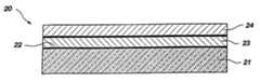
- a structure 20includes a substrate assembly 21 and a RuSi x O y -containing diffusion barrier layer 23 disposed on a surface 22 of the substrate assembly 21 , e.g., a silicon-containing substrate.
- the structure 20further includes a conductive layer 24 .
- substrate assemblyrefers to either a semiconductor substrate such as the base semiconductor layer (e.g., base silicon layer of a wafer), a silicon layer deposited on another material (e.g., silicon on sapphire), or a semiconductor substrate having one or more layers, structures, and/or regions formed thereon or therein. It is understood that reference to a substrate assembly herein also includes any known process steps that may have been previously used to form or define regions, junctions, various structures or features, and openings (e.g., vias, contact openings, high aspect ratio openings, etc.).
- the structure 20is representative of a RuSi x O y -containing diffusion barrier layer that may be used for any application requiring an effective barrier layer, for example, to prevent oxidation of an underlying Si contact, or to prevent diffusion into an electrode or dielectric from a silicon-containing surface.
- the RuSi x O y -containing diffusion barrier layer 23may be used in the fabrication of semiconductor devices or assemblies where it is necessary or desirable to prevent diffusion of one material to an adjacent material. As described more fully hereinafter, the RuSi x O y -containing diffusion barrier layer 23 may include Ru and/or RuSi x , in addition to RuSi x O y .
- the substrate assembly 21may, for example, be representative of a contact structure having an opening extending to a silicon-containing surface.
- diffusion barriersare commonly used within the contact opening to prevent undesirable reactions, such as reactions between the conductive contact material and the silicon-containing surface.
- the RuSi x O y -containing diffusion barrier layer 23may be used to form storage cell capacitors in semiconductor devices (e.g., memory devices).
- the RuSi x O y -containing diffusion barrier layer 23may be interposed between other layers of materials (e.g., ruthenium oxide, platinum, etc.) forming an electrode of a capacitor.
- diffusion barriers of the present inventioncan be used in any semiconductor processes, structures, assemblies and devices (e.g., CMOS devices and memory devices) which utilize barrier layers.
- the amount of elemental Si and SiO 2 incorporated into the RuSi x O y -containing diffusion barrier layer 23is sufficient to accomplish barrier characteristics for semiconductor devices, particularly for diffusion of silicon and oxygen, for example, into the electrode and/or dielectric of a capacitor.
- the RuSi x O y -containing diffusion barrier layer 23includes an atomic composition such that x and y are in the range of about 0.01 to about 10. More preferably, x and y are in the range of about 1 to about 3, and yet more preferably, x is about 0.4 and y is about 0.1.
- the RuSi xincludes an atomic composition such that x is in the range of about 0.01 to about 10, and more preferably in the range of about 0.1 to about 0.5, and yet more preferably, x is about 0.4.
- the thickness of the RuSi x O y -containing diffusion barrier layer 23is dependent upon the application for which it is used. Preferably, the thickness is in the range of about 10 ⁇ to 5,000 ⁇ . More preferably, the thickness of the RuSi x O y -containing diffusion barrier layer 23 is in the range of about 50 ⁇ to about 500 ⁇ . For example, this preferred thickness range of about 50 ⁇ to about 500 ⁇ is applicable to a RuSi x O y -containing diffusion barrier layer used for forming a bottom electrode stack of a capacitor structure.
- the conductive layer 24 shown in FIG. 1is representative of one or more layers.
- the conductive layer 24may include one or more layers formed of a metal or metal oxide, or combinations thereof. Such layers may include one of RuO 2 , MoO 2 , Rh, RhO 2 , IrO 2 , Ru, Pt, Pd and Ir, such as when the RuSi x O y -containing diffusion barrier layer is used in an electrode stack.
- the conductive layer 24may be a contact material, such as aluminum, when the RuSi x O y -containing diffusion barrier layer is used in a contact or interconnect application.
- Such conductive layersmay be formed by any method known to those skilled in the art.
- the RuSi x O y -containing diffusion barrier layer 23may be formed by various processes.
- the formation of the RuSi x O y -containing diffusion barrier layer 23may be sputter deposited from a deposition target of RuSi x O y , may be deposited by the sputtering from a deposition target of ruthenium onto a silicon-containing surface followed by an anneal, may be deposited by physical vapor deposition (PVD) of Ru—RuSi x —RuSi x O y mixed films, or may be deposited by CVD using a ruthenium precursor and a silicon precursor in an oxidizing atmosphere, or may be deposited by CVD of Ru—RuSi x —RuSi x O y films.
- PVDphysical vapor deposition
- Suitable CVD processesinclude, for example, atmospheric pressure chemical vapor deposition, low pressure chemical vapor deposition (LPCVD), plasma enhanced chemical vapor deposition (PECVD), or any other known chemical vapor deposition technique.
- LPCVDlow pressure chemical vapor deposition
- PECVDplasma enhanced chemical vapor deposition
- the RuSi x O y -containing diffusion barrier layermay be formed by depositing a layer of ruthenium using CVD onto a silicon-containing surface followed by an annealing process.
- the aforementioned CVD processesmay be carried out in a chemical vapor deposition reactor, such as a reaction chamber available under the trade designation of 7000 from Genus, Inc. (Sunnyvale, Calif.), a reaction chamber available under the trade designation of 5000 from Applied Materials, Inc. (Santa Clara, Calif.), or a reaction chamber available under the trade designation of Prism from Novelus, Inc. (San Jose, Calif.).
- a chemical vapor deposition reactorsuch as a reaction chamber available under the trade designation of 7000 from Genus, Inc. (Sunnyvale, Calif.), a reaction chamber available under the trade designation of 5000 from Applied Materials, Inc. (Santa Clara, Calif.), or a reaction chamber available under the trade designation of Prism from Novelus, Inc. (San Jose, Calif.).
- any reaction chamber suitable for performing CVDmay be used.
- Oxidizing agents for use in the CVD processmay be any gaseous reactant which is capable of reacting with the Ru precursor compounds at the decomposition temperatures of the latter to form Ru—RuSi x —RuSi x O y films.
- Suitable oxidizing agents for use with the present methodinclude, but are not limited to, air, oxygen, and oxygen-containing compounds, such as nitrous oxide, tetrahydrofuran, and carbon dioxide, and are preferably selected from mildly oxidizing gaseous oxygen sources.
- CVDmay be defined as the formation of a nonvolatile solid film on a substrate by the reaction of vapor phase reactants, i.e., reactant gases, that contain desired components.
- the reactant gasesare introduced into the reaction chamber.
- the gasesdecompose and react at a heated wafer surface to form the desired layer.
- Chemical vapor depositionis just one process of providing thin layers on semiconductor wafers, such as films of elemental metals or compounds (e.g., platinum, ruthenium oxide, iridium, molybdenum oxide, etc). Chemical vapor deposition processes are favored in many respects because of the process capability to provide highly conformal layers even within deep contacts and other openings. Thus, as described further below with reference to FIGS.
- CVD processingis preferably used to provide highly conformal layers within deep contacts and other openings such as for lower electrodes of storage cell capacitors. It will be readily apparent to one skilled in the art that although CVD is the preferred process, that the CVD process may be enhanced by various related techniques such as plasma assistance, photo assistance, laser assistance, as well as other techniques. In addition, atomic layer deposition could be used to form conformal layers. This is a variant of CVD in which a single atomic layer is formed on the surface. The layer thickness is self limiting to ⁇ 1 atomic layer. This layer is exposed to reaction gas after pump down or purge, is fully reacted, and the reaction gas pumped away. The process is repeated to yield the desired number of layers.
- atomic layer depositioncould be used to form the layer.
- This processis a special type of CVD in which, based on the process conditions and/or chemistry used, at most, a single layer comprising a single type of atom is deposited at one time. Accordingly, the thickness of the layer is, at most, the thickness of the relevant atom; hence, the layer may be referred to as a “monolayer.”
- the deposition gasis purged and a second monolayer comprising a different type of atom is deposited over the first monolayer. Additional monolayers may be provided in a similar manner, provided the gases from earlier deposition steps are purged from the chamber before each subsequent monolayer is deposited. Once at least two monolayers have been deposited, they may be reacted.
- One preferred method of forming the RuSi x O y -containing diffusion barrier layer 23is by depositing RuSi x , by CVD.
- the CVD processis conducted with a ruthenium precursor being delivered to a reaction chamber along with a silicon precursor.
- Typical ruthenium precursors in useinclude liquid ruthenium metal-organic precursors.
- the ruthenium precursoris contained in a bubbler reservoir through which a carrier gas, such as helium or any other inert gas, i.e., a gas that is nonreactive with other gases of the process (e.g., nitrogen, argon, neon, and xenon), is bubbled through the reservoir containing the precursor to deliver the precursor to the reaction chamber.
- a carrier gas having a volumetric flow rate in the range of about one sccm to about 500 sccmmay be used in a bubbler having a pressure in the range of about 0.5 torr to about 50 torr and a temperature in the range of about 30° C. to about 70° C. to deliver a ruthenium precursor to the reaction chamber.
- the ruthenium precursorsare liquid ruthenium complexes of the following formula (Formula I): (diene)Ru(CO) 3 wherein: “diene” refers to linear, branched, or cyclic dienes, bicyclic dienes, tricyclic dienes, fluorinated derivatives thereof, combinations thereof, and derivatives thereof additionally containing heteroatoms such as halide, Si, S, Se, P, As, or N.
- dierefers to linear, branched, or cyclic dienes, bicyclic dienes, tricyclic dienes, fluorinated derivatives thereof, combinations thereof, and derivatives thereof additionally containing heteroatoms such as halide, Si, S, Se, P, As, or N.
- the ruthenium precursors used according to the present inventioninclude one of C 6 H 8 Ru(CO) 3 ,(C 7 H 10 )Ru(CO) 3 , bis(cyclopentadienyl) ruthenium (II), triruthenium dodecacarbonyl, and cyclopentadienyl dicarbonyl ruthenium (II) dimer.
- the silicon precursoris also provided to the reaction chamber.
- the silicon precursormay include a silicon hydride or silane such as dichlorosilane (DCS, SiH 2 Cl 2 ), silane (SiH 4 ), disilane (H 3 SiSiH 3 ), trichlorosilane (TCS, SiHCl 3 ), or any other silicon precursor as would be recognized by one skilled in the art.
- the silicon precursormay be provided to the reaction chamber at a rate in the range of about 0.1 sccm to about 500 sccm. Preferably, the rate is about 10 sccm.
- the manner in which the gases are introduced into the reaction chambermay include one of various techniques.
- the introductionmay be accomplished with the use of compounds which are gases at room temperature or by heating a volatile compound and delivering the volatile compound to the reaction chamber using a carrier gas.
- solid precursors and various methods of vaporizing such solid precursorsmay also be used for introduction of reactant compounds into the chamber.
- the present inventionis not limited to any particular technique.
- reactant gasescan be admitted at separate inlet ports.
- an optional carrier or dilution gasi.e., a gas that is nonreactive with the reactant gases
- a carrier or dilution gasmay also be introduced into the chamber such as to change the concentrations of the gases therein.
- argon gasmay be introduced into the chamber at a varied flow rate.
- Oxidizing gasescan also be introduced into the reaction chamber when an oxidizing atmosphere is desired.
- the reaction chamber pressureis preferably maintained at a deposition pressure of about 0.1 torr to about 10 torr.
- the deposition temperature at the wafer surface upon which the RuSi x O y -containing diffusion barrier layer 23 is depositedis preferably held at a temperature in a range of about 100° C. to about 700° C., more preferably in the range of about 200° C. to about 500° C.
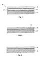
- FIGS. 2-4Another preferred method of forming a RuSi x O y -containing diffusion barrier layer 29 according to the present invention is shown in FIGS. 2-4.
- This methodforms the RuSi x O y -containing diffusion barrier layer 29 by depositing a layer of ruthenium 28 as shown in FIG. 2 onto a silicon-containing region of substrate assembly 26 using a CVD technique.
- the methodcan be carried out by introducing a ruthenium precursor composition into a CVD chamber together with a carrier or dilution gas, as described in Applicant's Assignees' copending patent application entitled “Methods for Preparing Ruthenium Oxide Films,” having Ser. No. 09/140,932, the contents of which are incorporated by reference herein.
- This ruthenium deposition stepis followed by an annealing process to react the silicon-containing region having silicon-containing surface 27 with the ruthenium layer 28 .
- the annealing processis carried out in an oxidizing atmosphere, such as oxygen gas, to further oxidize the deposited layer and to form the RuSi x O y -containing diffusion barrier layer 29 shown in FIG. 3 .
- oxidizing atmospheresuch as oxygen gas
- Various combinations of carrier gases and/or reaction (oxidizing) gasescan be used in the methods of the present invention.
- the gasescan be introduced into the CVD deposition chamber in a variety of manners, such as directly into a vaporization chamber of the CVD deposition chamber or in combination with the ruthenium precursor composition.
- a conductive layer 31e.g., the conductive layer 24 of FIG. 1 is formed on the RuSi x O y -containing diffusion barrier layer 29 , as shown in FIG. 4 .
- the annealing processis preferably performed in situ in the reaction chamber in a nitrogen atmosphere, although any other nonreactive atmosphere may be used, e.g., argon.
- the annealing temperatureis within the range of about 400° C. to about 1000° C., more preferably about 500° C.
- the annealis preferably performed for a time period of about 0.5 minutes to about 60 minutes.
- One of ordinary skill in the artwill recognize that such temperatures and time periods may vary and that the anneal parameters should be sufficient to convert the ruthenium layer 28 , following oxidation, into RuSi x O y -containing diffusion barrier layer 29 , where x and y are in the ranges previously described herein.
- anneal techniquese.g., furnace anneals, anneal, process RTP, and rapid thermal smearing
- the ruthenium layer 28 deposited for forming the RuSi x O y -containing diffusion barrier layer 29is preferably of a thickness in the range of about 10 ⁇ to about 1000 ⁇ . More preferably, the thickness is in the range is about 50 ⁇ to about of 500 ⁇ and, even more preferably, the thickness is about 300 ⁇ .
- a structure 30which includes a substrate assembly 32 , e.g., a silicon substrate region, and a stack 34 .
- the stack 34includes conductive layers 41 - 44 .
- One or more of the conductive layers 41 - 44may be RuSi x O y -containing diffusion barrier layers according to the present invention.
- the one or more conductive layers, in addition to including one or more RuSi x O y -containing diffusion barrier layers,may include conductive layers formed of various conductive materials.
- the conductive layersmay include, but are not limited to, layers formed of metals, metal oxides or combinations thereof.
- the conductive layersmay include metals such as rhodium, palladium, ruthenium, platinum, and iridium or metal oxides such as ruthenium oxide, rhodium oxide, molybdenum oxide and iridium oxide.
- the stack 34may be used for various applications, such as, interconnection applications and capacitor applications.
- the stack 34may be used as an electrode for a storage cell capacitor with substrate assembly 32 including a silicon-containing surface 33 .
- the barrier properties of the stack 34prevent silicon diffusion from silicon-containing surface 33 .
- the layer 41may be formed as the RuSi x O y -containing diffusion barrier layer to prevent diffusion of silicon from silicon-containing surface 33 through stack 34 to adjacent layer or layers 39 or to the surface of the stack 34 , and to prevent oxygen diffusion to the silicon-containing surface.
- FIG. 6shows a structure 50 including substrate assembly 52 , e.g., a silicon substrate, and capacitor structure 54 formed relative thereto.
- Capacitor structure 54includes a first electrode 56 , a second electrode 60 , and a high dielectric constant layer 58 interposed therebetween.
- the dielectric layermay be any suitable material having a desirable dielectric constant, such as, for example, Ba x Sr (1-x) TiO 3 [BST], BaTiO 3 , SrTiO 3 , PbTiO 3 , Pb(Zr,Ti)O 3 [PZT], (Pb,La)(Zr,Ti)O 3 [PLZT], (Pb,La)TiO 3 [PLT], Ta 2 O 5 , KNO 3 , and/or LiNbO 3 .
- a desirable dielectric constantsuch as, for example, Ba x Sr (1-x) TiO 3 [BST], BaTiO 3 , SrTiO 3 , PbTiO 3 , Pb(Zr,Ti)O 3 [PZT], (Pb,La)(Zr,Ti)O 3 [PLT], Ta 2 O 5 , KNO 3 , and/or LiNbO 3 .
- a desirable dielectric constantsuch as, for
- the electrode layer or electrode stackIn a bottom electrode of a capacitor structure, such as that shown in FIG. 6, the electrode layer or electrode stack must act as an effective barrier to the diffusion of silicon, particularly due to the high temperature processes used to form the high dielectric constant materials. Such diffusion barrier properties are particularly essential when the substrate assembly 52 includes a silicon-containing surface 53 (e.g., polysilicon, silicon substrate material, N-doped silicon, P-doped silicon) upon which the capacitor is formed, due to oxidation of the diffused silicon which may result in degraded capacitance, such as that seen in memory devices. Additionally, the electrode stack must act as an oxygen barrier to protect the silicon-containing surface under the stack from oxidizing. The formation of the RuSi x O y -containing diffusion barrier layer enhances the barrier properties of the stack.
- the first electrode 56includes one or more RuSi x O y -containing diffusion barrier layers and one or more additional conductive layers, as described with reference to FIG. 5 .
- the RuSi x O y -containing diffusion barrier layers of the present inventionhave numerous and varied applications in the area of semiconductor device and semiconductor structure fabrication. For example, the use of RuSi x O y -containing diffusion barrier layers of the present invention is described with reference to FIG. 7, wherein a contact liner requiring diffusion barrier characteristics is described. More specifically, device structure 70 is fabricated in accordance with conventional processing techniques through the formation of contact opening 102 prior to metallization of the contact area 94 of substrate 80 . As such, prior to metallization, the device structure 70 includes field oxide region 82 and active areas (represented by regions of substrate 80 not covered by field oxide). Word line 92 and field effect transistor (FET) 90 are formed relative to the field oxide regions 82 in the active areas.
- FETfield effect transistor
- doped source/drain regions 84 , 86are formed by conventional methods known to one of ordinary skill in the art.
- a conformal layer of oxide material 88is formed thereover and contact opening 102 is defined therein to the contact area 94 of doped source region 84 of silicon substrate 80 .
- one or more metallization or conductive layersare formed in the contact opening 102 for providing electrical connection to source region 84 .
- contact liner 100is a RuSi x O y -containing diffusion barrier layer formed according to the present invention on bottom surface 96 and the one or more side walls 98 defining the contact opening 102 .
- the RuSi x O y -containing diffusion barrier layeris generally deposited over the entire substrate assembly and then planarized to form the contact liner 100 . Thereafter, a conductive material 104 (e.g., aluminum, W, Cu) is formed in the contact opening for providing connection to doped source region 84 of substrate 80 .
- a conductive material 104e.g., aluminum, W, Cu
- the present inventionmay be used to fabricate a bottom electrode of a high dielectric capacitor of a storage cell that includes one or more RuSi x O y -containing diffusion barrier layers, as described in FIG. 8 .
- a device structure 106is fabricated in accordance with conventional processing techniques through the formation of an opening 114 prior to depositing a bottom electrode structure 118 on the surface 112 (preferably a silicon-containing surface) and surface 116 defining the opening 114 .
- a bottom electrode structure 118which includes a RuSi x O y -containing diffusion barrier layer, and one or more other conductive layers is formed in opening 114 according to the present invention, as previously described herein.
- the substrate assembly 110may include various elements, such as field oxide regions, active regions (i.e., regions of a silicon substrate not covered by field oxide) word lines, field effect transistors (FET), and source/drain regions created in the silicon substrate.
- An insulative layer of oxide material 113is formed over the substrate assembly.
- the opening 114 in the insulative layer of oxide material 113is a small, high aspect ratio opening.
- small, high aspect ratio openingshave feature sizes or critical dimensions below about 1 micron (e.g., such as a diameter or width of an opening being less than about 1 micron) and aspect ratios (ratio of depth to width) greater than about 4.
- Such aspect ratiosare applicable to contact holes, vias, trenches, and any other configured openings.
- a trench having an opening of 1 micron and depth of 3 micronshas an aspect ratio of 3.
- the present inventionis particularly useful in the formation of diffusion barrier layers in small, high aspect ratio features due to the use of CVD processes for forming conformal RuSi x O y -containing diffusion barrier layers over step structures.
- a bottom electrode structure 118including an RuSi x O y -containing diffusion barrier layer, is formed on the surface 112 and the one or more surfaces 116 defining opening 114 .
- the electrode stack layersare formed over the entire structure, including the surface 112 and surface 116 .
- the layersare then formed into bottom electrode structure 118 .
- the stack layersmay be etched or planarized to remove desired regions for forming the bottom electrode structure 118 .
- dielectric layer 120is formed relative to the bottom electrode structure 118 .
- the second electrode 192is then formed relative to the dielectric material 120 .
- Such an electrodemay, for example, be composed of any suitable conductive material, such as tungsten nitride, titanium nitride, tantalum nitride, ruthenium, rhodium, iridium, ruthenium oxide, iridium oxide, any combination thereof, or any other conductive material typically used as an electrode or electrode layer of a storage cell capacitor.
- the bottom electrodeis conformally formed of a stack of layers, including a RuSi x O y -containing diffusion barrier layer, having uniform thickness and deposited using CVD processes to provide suitable barrier properties.
- any capacitor formed relative to a surfacee.g., silicon-containing surface
- a surfacee.g., silicon-containing surface
- container capacitorstypically include electrodes formed on surfaces requiring conformal formation of a bottom electrode.
- Such a container capacitor storage cellis described in U.S. Pat. No. 5,270,241 to Dennison, et al., entitled “Optimized Container Stack Capacitor DRAM Cell Utilizing Sacrificial Oxide Deposition and Chemical Mechanical Polishing,” issued Dec. 14, 1993, and incorporated herein by this reference.
- the present inventionmay also be employed in the fabrication of other semiconductor processes and structures for various devices (e.g., CMOS devices, memory devices, logic devices, etc.). It should be understood that the present invention is not limited to the illustrative embodiments described herein and that the RuSi x O y -containing diffusion barrier layer of the present invention may be used for any application requiring diffusion barrier characteristics, particularly those for preventing diffusion of silicon and/or oxygen into adjacent layers.
- FIGS. 9 through 12show x-ray photo-electron spectrographic (XPS) depth profiles of sample wafers including layers containing RuO 2 , Si, and TiN layers, and additionally having a RuSi x O y diffusion barrier layer therein.
- the RuSi x O y diffusion barrier layerwas formed by a conventional CVD process.
- a pre-anneal and post-anneal XPS analysiswas conducted to determine the chemical state of the silicon and whether the TiN survived the anneal process.
- the depth profilewas determined for the sample wafer after the structure had undergone rapid thermal nitridation (RTN) at a temperature of about 700° C. for a time period of about 60 seconds.
- RTNrapid thermal nitridation
- the RuO 2 filmdisporportionates to Ru+RuO 4 and will oxidize the TiN if no barrier is present.
- the analytical datashows that no oxidation or silicidation of the TiN layer was observed and that minimal, if any, silicon diffusion through the RuSi x O y diffusion barrier layer and, therefore, no oxidation of the silicon layer in the tested samples was observed.
- the reaction chamber used for fabricating the sample waferwas a CVD chamber manufactured by MDC Vacuum Products Corp. (Hayward, Calif.) and the bubblers used are glass research bubblers from Technical Glass Service (Boise, Id.).
- the conditions used for forming the RuSi x O y -containing diffusion barrier layerinclude:
- Reaction Chamber Conditionspressure of 0.5 torr, deposition temperature of 240° C. at wafer surface, 0.2 sccm Si 2 H 6 .
- the conditions used for the forming the ruthenium oxide layerinclude:
- Reaction Chamber Conditionspressure of 3 torr, deposition temperature of 230° C. at wafer surface.
- the depth profilewas attained by using an XPS device available under the trade designation PhI ( ⁇ ) 5600 from Physical Electronics (Eden Prairie, Minn.).
- Sputteringwas performed with a 3 keV Argon ion beam restored over a 3 mm area. The sputter time for the depth profile of was 20 minutes.
- FIG. 9shows a depth profile of a sample wafer including a RuO 2 layer having a thickness of about 700 ⁇ formed over a Ru/RuSi x O y layer having a thickness of about 300 ⁇ formed on a SiO 2 substrate.
- FIG. 9shows the films as deposited before any oxidizing anneals and, thus, represents a control.
- FIG. 10shows the same film as described in FIG. 9 after undergoing RTN.
- the structurehas undergone RTN at a temperature of about 700° C. for a time period of 60 seconds, that is, when the RuO 2 layer is subjected to RTN, it produces RuO 4 .
- the Ru/RuSi x O y layerIn the absence of the Ru/RuSi x O y layer, the underlying TiN layer would be completely oxidized. However, due to the presence of the Ru/RuSi x O y layer, an effective barrier is created, thus preventing oxidation of the underlying layer (i.e., TiN layer).
- FIG. 11represents a depth profile of a sample wafer as described in reference to FIGS. 9 and 10, except that the RuSi layer was deposited using 5 SCCM of N 2 O as an oxidizer (40 SCCM He carrier 0.2 SCCM Si 2 H 6 at 260° C. and 3 torr).
- the XPS atomic concentration depth profile of this pre-RTN sampleindicates the presence of a SiO 2 -containing RuSi x layer having a thickness of about 500 ⁇ .
- FIG. 12represents a depth profile of a sample wafer as described in reference to FIG. 11, except that RuSi x layer was deposited in the absence of an oxidizer.
- the XPS atomic concentration depth profile of this pre-RTN sampleindicates the presence of a SiO 2 -containing RuSi x layer having a thickness of about 350 ⁇ on a TiN layer.
- no RuSi xwas detected in the Ru-containing film, only RuSi x O y .
- FIGS. 11 and 12indicate that the amount of oxygen in RuSi x O y film can actually be reduced by using N 2 O as a reaction gas presumably since small amounts of N 2 O increase growth rate without being incorporating.
- the present inventionmay be carried out to include controlled deposition of one or more “monolayers” of RuSi x O y -containing barrier layer(s).
- This processtypically referred to as atomic layer deposition, atomic layer epitaxy, sequential layer deposition, or pulsed-gas CVD, involves use of a precursor based on self-limiting surface reactions. Generally, a substrate is exposed to a first species that deposits as a monolayer and the monolayer then being exposed to a second species to form a new layer plus gaseous byproducts. The process is typically repeated until a desired thickness is achieved. Atomic layer deposition and various methods to carry out the same are described in U.S.
- the processhas also been described as a CVD operation performed under controlled conditions which cause the deposition to be self-limiting to yield deposition of, at most, a monolayer.
- the deposition of a monolayeris significant in many areas because it facilitates theoretically conformal films, precise control of film thickness, and improved compound material layer uniformity. In practice, however, the deposited “monolayer” is rarely a complete and true monolayer, there always being something less than complete coverage of an underlying layer or other surface, due to the space consumed by the non-incorporating components of the metal organic precursor.
- Combinations of deposition processes discussed hereinmay be used to provide deposition materials (e.g., atomic layer deposition (ALD) and non-ALD types of CVD).
- ALDatomic layer deposition
- CVDnon-ALD types of CVD
- exemplary embodiments of the inventioninclude within their scope deposition of a monolayer under conditions designed to achieve such results, as well as conditions with a subsequent shift of conditions toward the CVD regime, such that, to the extent required, the deposition of the RuSi x O y -containing barrier layers is effected as 3-5 “monolayers” rather than a single monolayer.
- deposition of monolayersis accomplished in a CVD chamber, as previously described with reference to the CVD deposition method, but with the addition of pulsing valves to allow the switching between the precursor and purge gas and the SiH 4 (Si 2 H 6 ) and purge gas. Bubblers, however, are not required since carrier gases may or may not be used, depending on the configuration of the vacuum system. For this example, a simple storage ampule with a single outlet and no inlet is used. As with the CVD method, C 6 H 8 Ru(CO) 3 is used as the ruthenium precursor. The deposition temperature of the wafer surface is 50-250 degrees C. and the reaction chamber is kept at a variable pressure range of about 0.5 torr to about 0.0001 torr.
- the reaction chamberis fully opened to the pumps of the vacuum system to create a vacuum in the CVD chamber and the ruthenium precursor gas is introduced at low pressure, preferably about 0.0001 torr. Introduction of the ruthenium precursor gas under these conditions will result in the deposition of, at most, a monolayer of ruthenium over the surface of the wafer.
- a purge cycleis then initiated by introducing a nonreactive gas, such as He or Ar, at a volumetric flow rate of about 50 sccm into the reaction chamber at 0.5 torr. It is understood that any suitable nonreactive gas may be used and that the nonreactive gas may be introduced at a rate of between about 0.1 sccm to about 500 sccm to optimize system conditions.
- Silane or disilaneis introduced into the reaction chamber at a rate of about 5 sccm, which results in the deposition of a silicon monolayer over the previously deposited ruthenium monolayer. This is followed by a purge cycle of nonreactive gas, as previously described. It is understood that oxygen can be added as a separate oxygen/purge cycle as needed for every individual cycle in order to give the required oxygen content. In general, however, sufficient oxygen is available from background O 2 and H 2 O in the chamber to oxidize the underlying RuSi x layer formed in the preceding steps.
- the monolayer of adsorbed precursor from the initial precursor deposition stepwill react directly when exposed to the reaction gas in the third step of the foregoing dose precursor/purge/dose reaction gas/purge sequence, which results in controlled deposition of one or more RuSi x O y -containing barrier monolayers.
Landscapes
- Engineering & Computer Science (AREA)
- Physics & Mathematics (AREA)
- Computer Hardware Design (AREA)
- Condensed Matter Physics & Semiconductors (AREA)
- General Physics & Mathematics (AREA)
- Microelectronics & Electronic Packaging (AREA)
- Power Engineering (AREA)
- Manufacturing & Machinery (AREA)
- Plasma & Fusion (AREA)
- Chemical & Material Sciences (AREA)
- Chemical Kinetics & Catalysis (AREA)
- General Chemical & Material Sciences (AREA)
- Semiconductor Memories (AREA)
Abstract
Description
Claims (20)
Priority Applications (1)
| Application Number | Priority Date | Filing Date | Title |
|---|---|---|---|
| US10/136,771US6744138B2 (en) | 2000-08-30 | 2002-04-30 | RuSixOy-containing barrier layers for high-k dielectrics |
Applications Claiming Priority (2)
| Application Number | Priority Date | Filing Date | Title |
|---|---|---|---|
| US09/651,620US6903005B1 (en) | 2000-08-30 | 2000-08-30 | Method for the formation of RuSixOy-containing barrier layers for high-k dielectrics |
| US10/136,771US6744138B2 (en) | 2000-08-30 | 2002-04-30 | RuSixOy-containing barrier layers for high-k dielectrics |
Related Parent Applications (1)
| Application Number | Title | Priority Date | Filing Date |
|---|---|---|---|
| US09/651,620DivisionUS6903005B1 (en) | 2000-08-30 | 2000-08-30 | Method for the formation of RuSixOy-containing barrier layers for high-k dielectrics |
Publications (2)
| Publication Number | Publication Date |
|---|---|
| US20020121697A1 US20020121697A1 (en) | 2002-09-05 |
| US6744138B2true US6744138B2 (en) | 2004-06-01 |
Family
ID=24613557
Family Applications (4)
| Application Number | Title | Priority Date | Filing Date |
|---|---|---|---|
| US09/651,620Expired - Fee RelatedUS6903005B1 (en) | 2000-08-30 | 2000-08-30 | Method for the formation of RuSixOy-containing barrier layers for high-k dielectrics |
| US10/136,771Expired - LifetimeUS6744138B2 (en) | 2000-08-30 | 2002-04-30 | RuSixOy-containing barrier layers for high-k dielectrics |
| US10/215,991Expired - LifetimeUS6787449B2 (en) | 2000-08-30 | 2002-08-09 | Method for the formation of RuSixOy-containing barrier layers for high-k dielectrics |
| US10/215,990Expired - Fee RelatedUS6800521B2 (en) | 2000-08-30 | 2002-08-09 | Process for the formation of RuSixOy-containing barrier layers for high-k dielectrics |
Family Applications Before (1)
| Application Number | Title | Priority Date | Filing Date |
|---|---|---|---|
| US09/651,620Expired - Fee RelatedUS6903005B1 (en) | 2000-08-30 | 2000-08-30 | Method for the formation of RuSixOy-containing barrier layers for high-k dielectrics |
Family Applications After (2)
| Application Number | Title | Priority Date | Filing Date |
|---|---|---|---|
| US10/215,991Expired - LifetimeUS6787449B2 (en) | 2000-08-30 | 2002-08-09 | Method for the formation of RuSixOy-containing barrier layers for high-k dielectrics |
| US10/215,990Expired - Fee RelatedUS6800521B2 (en) | 2000-08-30 | 2002-08-09 | Process for the formation of RuSixOy-containing barrier layers for high-k dielectrics |
Country Status (1)
| Country | Link |
|---|---|
| US (4) | US6903005B1 (en) |
Cited By (14)
| Publication number | Priority date | Publication date | Assignee | Title |
|---|---|---|---|---|
| US20030193270A1 (en)* | 2002-04-11 | 2003-10-16 | Samsung Electro-Mechanics Co., Ltd. | Piezoelectric transformer device and housing for piezoelectric transformer and method of manufacturing them |
| US20040105934A1 (en)* | 2002-06-04 | 2004-06-03 | Mei Chang | Ruthenium layer formation for copper film deposition |
| US20040241321A1 (en)* | 2002-06-04 | 2004-12-02 | Applied Materials, Inc. | Ruthenium layer formation for copper film deposition |
| US20050220998A1 (en)* | 2002-06-04 | 2005-10-06 | Applied Materials, Inc. | Noble metal layer formation for copper film deposition |
| US20060199372A1 (en)* | 2005-03-01 | 2006-09-07 | Applied Materials, Inc. | Reduction of copper dewetting by transition metal deposition |
| WO2007050050A2 (en) | 2004-10-07 | 2007-05-03 | Merck & Co., Inc. | Thiazolyl mglur5 antagonists and methods for their use |
| US20070235059A1 (en)* | 2006-04-07 | 2007-10-11 | Applied Materials, Inc. | Method of recovering valuable material from exhaust gas stream of a reaction chamber |
| US7429402B2 (en) | 2004-12-10 | 2008-09-30 | Applied Materials, Inc. | Ruthenium as an underlayer for tungsten film deposition |
| US20080268171A1 (en)* | 2005-11-04 | 2008-10-30 | Paul Ma | Apparatus and process for plasma-enhanced atomic layer deposition |
| US20090087982A1 (en)* | 2007-09-28 | 2009-04-02 | Applied Materials, Inc. | Selective ruthenium deposition on copper materials |
| US7749815B2 (en) | 2001-07-16 | 2010-07-06 | Applied Materials, Inc. | Methods for depositing tungsten after surface treatment |
| US20100255653A1 (en)* | 2009-04-07 | 2010-10-07 | Micron Technology, Inc. | Semiconductor processing |
| US9960240B2 (en) | 2015-10-21 | 2018-05-01 | International Business Machines Corporation | Low resistance contact structures for trench structures |
| US10304773B2 (en) | 2015-10-21 | 2019-05-28 | International Business Machines Corporation | Low resistance contact structures including a copper fill for trench structures |
Families Citing this family (69)
| Publication number | Priority date | Publication date | Assignee | Title |
|---|---|---|---|---|
| US6776792B1 (en) | 1997-04-24 | 2004-08-17 | Advanced Cardiovascular Systems Inc. | Coated endovascular stent |
| US6197628B1 (en)* | 1998-08-27 | 2001-03-06 | Micron Technology, Inc. | Ruthenium silicide diffusion barrier layers and methods of forming same |
| US6974766B1 (en) | 1998-10-01 | 2005-12-13 | Applied Materials, Inc. | In situ deposition of a low κ dielectric layer, barrier layer, etch stop, and anti-reflective coating for damascene application |
| US6620723B1 (en) | 2000-06-27 | 2003-09-16 | Applied Materials, Inc. | Formation of boride barrier layers using chemisorption techniques |
| US7964505B2 (en) | 2005-01-19 | 2011-06-21 | Applied Materials, Inc. | Atomic layer deposition of tungsten materials |
| US7732327B2 (en) | 2000-06-28 | 2010-06-08 | Applied Materials, Inc. | Vapor deposition of tungsten materials |
| US7101795B1 (en) | 2000-06-28 | 2006-09-05 | Applied Materials, Inc. | Method and apparatus for depositing refractory metal layers employing sequential deposition techniques to form a nucleation layer |
| US6551929B1 (en) | 2000-06-28 | 2003-04-22 | Applied Materials, Inc. | Bifurcated deposition process for depositing refractory metal layers employing atomic layer deposition and chemical vapor deposition techniques |
| US7405158B2 (en) | 2000-06-28 | 2008-07-29 | Applied Materials, Inc. | Methods for depositing tungsten layers employing atomic layer deposition techniques |
| US6783793B1 (en) | 2000-10-26 | 2004-08-31 | Advanced Cardiovascular Systems, Inc. | Selective coating of medical devices |
| DE10121132A1 (en)* | 2001-04-30 | 2002-10-31 | Infineon Technologies Ag | Method for producing a metallic or metal-containing layer using a precursor on a silicon- or germanium-containing layer, in particular an electronic component |
| US6849545B2 (en)* | 2001-06-20 | 2005-02-01 | Applied Materials, Inc. | System and method to form a composite film stack utilizing sequential deposition techniques |
| US6565659B1 (en) | 2001-06-28 | 2003-05-20 | Advanced Cardiovascular Systems, Inc. | Stent mounting assembly and a method of using the same to coat a stent |
| US7211144B2 (en) | 2001-07-13 | 2007-05-01 | Applied Materials, Inc. | Pulsed nucleation deposition of tungsten layers |
| TW581822B (en)* | 2001-07-16 | 2004-04-01 | Applied Materials Inc | Formation of composite tungsten films |
| US8110489B2 (en) | 2001-07-25 | 2012-02-07 | Applied Materials, Inc. | Process for forming cobalt-containing materials |
| US9051641B2 (en) | 2001-07-25 | 2015-06-09 | Applied Materials, Inc. | Cobalt deposition on barrier surfaces |
| JP2005504885A (en) | 2001-07-25 | 2005-02-17 | アプライド マテリアルズ インコーポレイテッド | Barrier formation using a novel sputter deposition method |
| US20090004850A1 (en) | 2001-07-25 | 2009-01-01 | Seshadri Ganguli | Process for forming cobalt and cobalt silicide materials in tungsten contact applications |
| US20030029715A1 (en) | 2001-07-25 | 2003-02-13 | Applied Materials, Inc. | An Apparatus For Annealing Substrates In Physical Vapor Deposition Systems |
| US6936906B2 (en) | 2001-09-26 | 2005-08-30 | Applied Materials, Inc. | Integration of barrier layer and seed layer |
| TW589684B (en)* | 2001-10-10 | 2004-06-01 | Applied Materials Inc | Method for depositing refractory metal layers employing sequential deposition techniques |
| US6809026B2 (en) | 2001-12-21 | 2004-10-26 | Applied Materials, Inc. | Selective deposition of a barrier layer on a metal film |
| US6998014B2 (en) | 2002-01-26 | 2006-02-14 | Applied Materials, Inc. | Apparatus and method for plasma assisted deposition |
| US6911391B2 (en) | 2002-01-26 | 2005-06-28 | Applied Materials, Inc. | Integration of titanium and titanium nitride layers |
| US6827978B2 (en) | 2002-02-11 | 2004-12-07 | Applied Materials, Inc. | Deposition of tungsten films |
| US6833161B2 (en) | 2002-02-26 | 2004-12-21 | Applied Materials, Inc. | Cyclical deposition of tungsten nitride for metal oxide gate electrode |
| US6720027B2 (en)* | 2002-04-08 | 2004-04-13 | Applied Materials, Inc. | Cyclical deposition of a variable content titanium silicon nitride layer |
| US6846516B2 (en) | 2002-04-08 | 2005-01-25 | Applied Materials, Inc. | Multiple precursor cyclical deposition system |
| US7279432B2 (en)* | 2002-04-16 | 2007-10-09 | Applied Materials, Inc. | System and method for forming an integrated barrier layer |
| US6838125B2 (en) | 2002-07-10 | 2005-01-04 | Applied Materials, Inc. | Method of film deposition using activated precursor gases |
| US6821563B2 (en) | 2002-10-02 | 2004-11-23 | Applied Materials, Inc. | Gas distribution system for cyclical layer deposition |
| US7262133B2 (en)* | 2003-01-07 | 2007-08-28 | Applied Materials, Inc. | Enhancement of copper line reliability using thin ALD tan film to cap the copper line |
| US20040229453A1 (en)* | 2003-05-15 | 2004-11-18 | Jsr Micro, Inc. | Methods of pore sealing and metal encapsulation in porous low k interconnect |
| US7211508B2 (en) | 2003-06-18 | 2007-05-01 | Applied Materials, Inc. | Atomic layer deposition of tantalum based barrier materials |
| US7198675B2 (en) | 2003-09-30 | 2007-04-03 | Advanced Cardiovascular Systems | Stent mandrel fixture and method for selectively coating surfaces of a stent |
| US7563324B1 (en) | 2003-12-29 | 2009-07-21 | Advanced Cardiovascular Systems Inc. | System and method for coating an implantable medical device |
| WO2005094440A2 (en)* | 2004-03-18 | 2005-10-13 | Nanosys Inc. | Nanofiber surface based capacitors |
| US7553377B1 (en) | 2004-04-27 | 2009-06-30 | Advanced Cardiovascular Systems, Inc. | Apparatus and method for electrostatic coating of an abluminal stent surface |
| US7202185B1 (en)* | 2004-06-22 | 2007-04-10 | Novellus Systems, Inc. | Silica thin films produced by rapid surface catalyzed vapor deposition (RVD) using a nucleation layer |
| US7297608B1 (en) | 2004-06-22 | 2007-11-20 | Novellus Systems, Inc. | Method for controlling properties of conformal silica nanolaminates formed by rapid vapor deposition |
| US7790633B1 (en) | 2004-10-26 | 2010-09-07 | Novellus Systems, Inc. | Sequential deposition/anneal film densification method |
| US7708835B2 (en)* | 2004-11-29 | 2010-05-04 | Tokyo Electron Limited | Film precursor tray for use in a film precursor evaporation system and method of using |
| US7488512B2 (en)* | 2004-11-29 | 2009-02-10 | Tokyo Electron Limited | Method for preparing solid precursor tray for use in solid precursor evaporation system |
| US7484315B2 (en)* | 2004-11-29 | 2009-02-03 | Tokyo Electron Limited | Replaceable precursor tray for use in a multi-tray solid precursor delivery system |
| US7638002B2 (en)* | 2004-11-29 | 2009-12-29 | Tokyo Electron Limited | Multi-tray film precursor evaporation system and thin film deposition system incorporating same |
| US7632307B2 (en) | 2004-12-16 | 2009-12-15 | Advanced Cardiovascular Systems, Inc. | Abluminal, multilayer coating constructs for drug-delivery stents |
| US7294583B1 (en) | 2004-12-23 | 2007-11-13 | Novellus Systems, Inc. | Methods for the use of alkoxysilanol precursors for vapor deposition of SiO2 films |
| US7482247B1 (en) | 2004-12-30 | 2009-01-27 | Novellus Systems, Inc. | Conformal nanolaminate dielectric deposition and etch bag gap fill process |
| US7135418B1 (en) | 2005-03-09 | 2006-11-14 | Novellus Systems, Inc. | Optimal operation of conformal silica deposition reactors |
| US7651570B2 (en)* | 2005-03-31 | 2010-01-26 | Tokyo Electron Limited | Solid precursor vaporization system for use in chemical vapor deposition |
| EP1866963A4 (en)* | 2005-04-07 | 2009-07-08 | Aviza Tech Inc | MULTICOMPOSING FILMS, MULTICOMPONENTS WITH A HIGH DIELECTRIC CONSTANT, AND METHODS OF DEPOSITING THESE FILMS |
| US7713876B2 (en)* | 2005-09-28 | 2010-05-11 | Tokyo Electron Limited | Method for integrating a ruthenium layer with bulk copper in copper metallization |
| US7589028B1 (en) | 2005-11-15 | 2009-09-15 | Novellus Systems, Inc. | Hydroxyl bond removal and film densification method for oxide films using microwave post treatment |
| US7867547B2 (en) | 2005-12-19 | 2011-01-11 | Advanced Cardiovascular Systems, Inc. | Selectively coating luminal surfaces of stents |
| US7491653B1 (en) | 2005-12-23 | 2009-02-17 | Novellus Systems, Inc. | Metal-free catalysts for pulsed deposition layer process for conformal silica laminates |
| US20070160756A1 (en)* | 2006-01-07 | 2007-07-12 | Helmuth Treichel | Apparatus and method for the deposition of ruthenium containing films |
| US7288463B1 (en) | 2006-04-28 | 2007-10-30 | Novellus Systems, Inc. | Pulsed deposition layer gap fill with expansion material |
| US8003156B2 (en) | 2006-05-04 | 2011-08-23 | Advanced Cardiovascular Systems, Inc. | Rotatable support elements for stents |
| US8603530B2 (en) | 2006-06-14 | 2013-12-10 | Abbott Cardiovascular Systems Inc. | Nanoshell therapy |
| US8048448B2 (en) | 2006-06-15 | 2011-11-01 | Abbott Cardiovascular Systems Inc. | Nanoshells for drug delivery |
| US7625820B1 (en) | 2006-06-21 | 2009-12-01 | Novellus Systems, Inc. | Method of selective coverage of high aspect ratio structures with a conformal film |
| US8017237B2 (en) | 2006-06-23 | 2011-09-13 | Abbott Cardiovascular Systems, Inc. | Nanoshells on polymers |
| US7846256B2 (en)* | 2007-02-23 | 2010-12-07 | Tokyo Electron Limited | Ampule tray for and method of precursor surface area |
| US8048441B2 (en) | 2007-06-25 | 2011-11-01 | Abbott Cardiovascular Systems, Inc. | Nanobead releasing medical devices |
| JP2009302166A (en)* | 2008-06-11 | 2009-12-24 | Panasonic Corp | Semiconductor device, and manufacturing method thereof |
| US8557702B2 (en)* | 2009-02-02 | 2013-10-15 | Asm America, Inc. | Plasma-enhanced atomic layers deposition of conductive material over dielectric layers |
| DE102010048620B4 (en)* | 2010-10-15 | 2013-03-28 | Epcos Ag | Electrode, microacoustic component and method of manufacturing an electrode |
| KR102257978B1 (en)* | 2014-03-17 | 2021-05-31 | 삼성디스플레이 주식회사 | Display divece and method for preparing the same |
Citations (38)
| Publication number | Priority date | Publication date | Assignee | Title |
|---|---|---|---|---|
| US4058430A (en) | 1974-11-29 | 1977-11-15 | Tuomo Suntola | Method for producing compound thin films |
| US4157943A (en) | 1978-07-14 | 1979-06-12 | The International Nickel Company, Inc. | Composite electrode for electrolytic processes |
| US4250210A (en) | 1977-12-27 | 1981-02-10 | The International Nickel Co., Inc. | Chemical vapor deposition |
| US4413022A (en) | 1979-02-28 | 1983-11-01 | Canon Kabushiki Kaisha | Method for performing growth of compound thin films |
| US4982309A (en) | 1989-07-17 | 1991-01-01 | National Semiconductor Corporation | Electrodes for electrical ceramic oxide devices |
| US5080862A (en) | 1990-04-25 | 1992-01-14 | General Electric Company | Iridium silicon alloy |
| US5122923A (en) | 1989-08-30 | 1992-06-16 | Nec Corporation | Thin-film capacitors and process for manufacturing the same |
| US5126016A (en) | 1991-02-01 | 1992-06-30 | International Business Machines Corporation | Circuitization of polymeric circuit boards with galvanic removal of chromium adhesion layers |
| US5130172A (en) | 1988-10-21 | 1992-07-14 | The Regents Of The University Of California | Low temperature organometallic deposition of metals |
| US5241137A (en) | 1989-06-30 | 1993-08-31 | Sharp Kabushiki Kaisha | Flexible circuit board with an electrically insulating adhesive layer |
| US5270241A (en) | 1992-03-13 | 1993-12-14 | Micron Technology, Inc. | Optimized container stacked capacitor DRAM cell utilizing sacrificial oxide deposition and chemical mechanical polishing |
| US5286675A (en) | 1993-04-14 | 1994-02-15 | Industrial Technology Research Institute | Blanket tungsten etchback process using disposable spin-on-glass |
| US5314727A (en) | 1992-07-28 | 1994-05-24 | Minnesota Mining & Mfg. Co./Regents Of The University Of Minnesota | Chemical vapor deposition of iron, ruthenium, and osmium |
| US5335138A (en) | 1993-02-12 | 1994-08-02 | Micron Semiconductor, Inc. | High dielectric constant capacitor and method of manufacture |
| US5352488A (en) | 1993-05-14 | 1994-10-04 | Syracuse University | Chemical vapor deposition process employing metal pentadienyl complexes |
| US5525181A (en) | 1991-10-31 | 1996-06-11 | U.S. Philips Corporation | Method of manufacturing a multilayer printed circuit board having first and second conducting patterns connected through an adhesive layer and laminate for the manufacture of such a printed circuit board |
| US5529953A (en) | 1994-10-14 | 1996-06-25 | Toshiba America Electronic Components, Inc. | Method of forming studs and interconnects in a multi-layered semiconductor device |
| US5614795A (en) | 1995-03-29 | 1997-03-25 | Samsung Display Devices Co., Ltd. | Field emission device |
| US5618761A (en) | 1994-09-16 | 1997-04-08 | Kabushiki Kaisha Toshiba | Method of manufacturing a perovskite thin film dielectric |
| US5637533A (en) | 1995-05-17 | 1997-06-10 | Hyundai Electronics Industries Co., Ltd. | Method for fabricating a diffusion barrier metal layer in a semiconductor device |
| US5662815A (en) | 1995-03-28 | 1997-09-02 | Samsung Display Devices Co., Ltd. | Fabricating method of a multiple micro-tip field emission device using selective etching of an adhesion layer |
| US5705442A (en) | 1995-10-27 | 1998-01-06 | Vanguard International Semiconductor Corporation | Optimized tungsten contact plug process via use of furnace annealed barrier layers |
| US5719425A (en) | 1996-01-31 | 1998-02-17 | Micron Technology, Inc. | Multiple implant lightly doped drain (MILDD) field effect transistor |
| US5729054A (en) | 1994-08-01 | 1998-03-17 | Texas Instruments Incorporated | Conductive noble-metal-insulator-alloy barrier layer for high-dielectric-constant material electrodes |
| US5742322A (en) | 1993-08-20 | 1998-04-21 | Ultra Silicon Technology(Uk) Limited | AC thin film electroluminescent device |
| US5843830A (en) | 1996-06-26 | 1998-12-01 | Micron Technology, Inc. | Capacitor, and methods for forming a capacitor |
| US5874174A (en) | 1995-08-09 | 1999-02-23 | Matsushita Electric Industrial Co., Ltd. | Conductor film and its forming method |
| US5885750A (en) | 1997-10-02 | 1999-03-23 | International Business Machines Corporation | Tantalum adhesion layer and reactive-ion-etch process for providing a thin film metallization area |
| US5962716A (en) | 1998-08-27 | 1999-10-05 | Micron Technology, Inc. | Methods for preparing ruthenium and osmium compounds |
| US5994034A (en) | 1996-04-19 | 1999-11-30 | Nec Corporation | Fabrication method of printed wiring board |
| US6063705A (en) | 1998-08-27 | 2000-05-16 | Micron Technology, Inc. | Precursor chemistries for chemical vapor deposition of ruthenium and ruthenium oxide |
| US6133159A (en) | 1998-08-27 | 2000-10-17 | Micron Technology, Inc. | Methods for preparing ruthenium oxide films |
| US6194753B1 (en)* | 1995-12-27 | 2001-02-27 | Hyundai Electronics Industries Co., Ltd. | Method of forming a perovskite structure semiconductor capacitor |
| US6197628B1 (en)* | 1998-08-27 | 2001-03-06 | Micron Technology, Inc. | Ruthenium silicide diffusion barrier layers and methods of forming same |
| US6320213B1 (en)* | 1997-12-19 | 2001-11-20 | Advanced Technology Materials, Inc. | Diffusion barriers between noble metal electrodes and metallization layers, and integrated circuit and semiconductor devices comprising same |
| US6407422B1 (en)* | 1999-04-23 | 2002-06-18 | Sony Corporation | Oxygen diffusion blocking semiconductor capacitor |
| US6429127B1 (en)* | 2000-06-08 | 2002-08-06 | Micron Technology, Inc. | Methods for forming rough ruthenium-containing layers and structures/methods using same |
| US6461909B1 (en) | 2000-08-30 | 2002-10-08 | Micron Technology, Inc. | Process for fabricating RuSixOy-containing adhesion layers |
Family Cites Families (3)
| Publication number | Priority date | Publication date | Assignee | Title |
|---|---|---|---|---|
| JPH0231042A (en) | 1988-07-20 | 1990-02-01 | Kayaba Ind Co Ltd | hydraulic shock absorber |
| US5612574A (en) | 1995-06-06 | 1997-03-18 | Texas Instruments Incorporated | Semiconductor structures using high-dielectric-constant materials and an adhesion layer |
| JPH0931042A (en) | 1995-07-19 | 1997-02-04 | Shionogi & Co Ltd | Medicinal composition containing carbamoylmethylurea derivative and intermediate for producing carbamoylmethylurea derivative |
- 2000
- 2000-08-30USUS09/651,620patent/US6903005B1/ennot_activeExpired - Fee Related
- 2002
- 2002-04-30USUS10/136,771patent/US6744138B2/ennot_activeExpired - Lifetime
- 2002-08-09USUS10/215,991patent/US6787449B2/ennot_activeExpired - Lifetime
- 2002-08-09USUS10/215,990patent/US6800521B2/ennot_activeExpired - Fee Related
Patent Citations (40)
| Publication number | Priority date | Publication date | Assignee | Title |
|---|---|---|---|---|
| US4058430A (en) | 1974-11-29 | 1977-11-15 | Tuomo Suntola | Method for producing compound thin films |
| US4250210A (en) | 1977-12-27 | 1981-02-10 | The International Nickel Co., Inc. | Chemical vapor deposition |
| US4157943A (en) | 1978-07-14 | 1979-06-12 | The International Nickel Company, Inc. | Composite electrode for electrolytic processes |
| US4413022A (en) | 1979-02-28 | 1983-11-01 | Canon Kabushiki Kaisha | Method for performing growth of compound thin films |
| US5130172A (en) | 1988-10-21 | 1992-07-14 | The Regents Of The University Of California | Low temperature organometallic deposition of metals |
| US5241137A (en) | 1989-06-30 | 1993-08-31 | Sharp Kabushiki Kaisha | Flexible circuit board with an electrically insulating adhesive layer |
| US4982309A (en) | 1989-07-17 | 1991-01-01 | National Semiconductor Corporation | Electrodes for electrical ceramic oxide devices |
| US5122923A (en) | 1989-08-30 | 1992-06-16 | Nec Corporation | Thin-film capacitors and process for manufacturing the same |
| US5080862A (en) | 1990-04-25 | 1992-01-14 | General Electric Company | Iridium silicon alloy |
| US5126016A (en) | 1991-02-01 | 1992-06-30 | International Business Machines Corporation | Circuitization of polymeric circuit boards with galvanic removal of chromium adhesion layers |
| US5525181A (en) | 1991-10-31 | 1996-06-11 | U.S. Philips Corporation | Method of manufacturing a multilayer printed circuit board having first and second conducting patterns connected through an adhesive layer and laminate for the manufacture of such a printed circuit board |
| US5270241A (en) | 1992-03-13 | 1993-12-14 | Micron Technology, Inc. | Optimized container stacked capacitor DRAM cell utilizing sacrificial oxide deposition and chemical mechanical polishing |
| US5314727A (en) | 1992-07-28 | 1994-05-24 | Minnesota Mining & Mfg. Co./Regents Of The University Of Minnesota | Chemical vapor deposition of iron, ruthenium, and osmium |
| US5372849A (en) | 1992-07-28 | 1994-12-13 | Minnesota Mining And Manufacturing Company | Chemical vapor deposition of iron, ruthenium, and osmium |
| US5335138A (en) | 1993-02-12 | 1994-08-02 | Micron Semiconductor, Inc. | High dielectric constant capacitor and method of manufacture |
| US5286675A (en) | 1993-04-14 | 1994-02-15 | Industrial Technology Research Institute | Blanket tungsten etchback process using disposable spin-on-glass |
| US5352488A (en) | 1993-05-14 | 1994-10-04 | Syracuse University | Chemical vapor deposition process employing metal pentadienyl complexes |
| US5742322A (en) | 1993-08-20 | 1998-04-21 | Ultra Silicon Technology(Uk) Limited | AC thin film electroluminescent device |
| US5729054A (en) | 1994-08-01 | 1998-03-17 | Texas Instruments Incorporated | Conductive noble-metal-insulator-alloy barrier layer for high-dielectric-constant material electrodes |
| US5618761A (en) | 1994-09-16 | 1997-04-08 | Kabushiki Kaisha Toshiba | Method of manufacturing a perovskite thin film dielectric |
| US5529953A (en) | 1994-10-14 | 1996-06-25 | Toshiba America Electronic Components, Inc. | Method of forming studs and interconnects in a multi-layered semiconductor device |
| US5662815A (en) | 1995-03-28 | 1997-09-02 | Samsung Display Devices Co., Ltd. | Fabricating method of a multiple micro-tip field emission device using selective etching of an adhesion layer |
| US5614795A (en) | 1995-03-29 | 1997-03-25 | Samsung Display Devices Co., Ltd. | Field emission device |
| US5637533A (en) | 1995-05-17 | 1997-06-10 | Hyundai Electronics Industries Co., Ltd. | Method for fabricating a diffusion barrier metal layer in a semiconductor device |
| US5874174A (en) | 1995-08-09 | 1999-02-23 | Matsushita Electric Industrial Co., Ltd. | Conductor film and its forming method |
| US5705442A (en) | 1995-10-27 | 1998-01-06 | Vanguard International Semiconductor Corporation | Optimized tungsten contact plug process via use of furnace annealed barrier layers |
| US6194753B1 (en)* | 1995-12-27 | 2001-02-27 | Hyundai Electronics Industries Co., Ltd. | Method of forming a perovskite structure semiconductor capacitor |
| US5866460A (en) | 1996-01-31 | 1999-02-02 | Micron Technology, Inc. | Method of forming a multiple inplant lightly doped drain (MILDD) field effect transistor |
| US5719425A (en) | 1996-01-31 | 1998-02-17 | Micron Technology, Inc. | Multiple implant lightly doped drain (MILDD) field effect transistor |
| US5994034A (en) | 1996-04-19 | 1999-11-30 | Nec Corporation | Fabrication method of printed wiring board |
| US5843830A (en) | 1996-06-26 | 1998-12-01 | Micron Technology, Inc. | Capacitor, and methods for forming a capacitor |
| US5885750A (en) | 1997-10-02 | 1999-03-23 | International Business Machines Corporation | Tantalum adhesion layer and reactive-ion-etch process for providing a thin film metallization area |
| US6320213B1 (en)* | 1997-12-19 | 2001-11-20 | Advanced Technology Materials, Inc. | Diffusion barriers between noble metal electrodes and metallization layers, and integrated circuit and semiconductor devices comprising same |
| US6133159A (en) | 1998-08-27 | 2000-10-17 | Micron Technology, Inc. | Methods for preparing ruthenium oxide films |
| US6063705A (en) | 1998-08-27 | 2000-05-16 | Micron Technology, Inc. | Precursor chemistries for chemical vapor deposition of ruthenium and ruthenium oxide |
| US6197628B1 (en)* | 1998-08-27 | 2001-03-06 | Micron Technology, Inc. | Ruthenium silicide diffusion barrier layers and methods of forming same |
| US5962716A (en) | 1998-08-27 | 1999-10-05 | Micron Technology, Inc. | Methods for preparing ruthenium and osmium compounds |
| US6407422B1 (en)* | 1999-04-23 | 2002-06-18 | Sony Corporation | Oxygen diffusion blocking semiconductor capacitor |
| US6429127B1 (en)* | 2000-06-08 | 2002-08-06 | Micron Technology, Inc. | Methods for forming rough ruthenium-containing layers and structures/methods using same |
| US6461909B1 (en) | 2000-08-30 | 2002-10-08 | Micron Technology, Inc. | Process for fabricating RuSixOy-containing adhesion layers |
Non-Patent Citations (15)
Cited By (36)
| Publication number | Priority date | Publication date | Assignee | Title |
|---|---|---|---|---|
| US7749815B2 (en) | 2001-07-16 | 2010-07-06 | Applied Materials, Inc. | Methods for depositing tungsten after surface treatment |
| US20030193270A1 (en)* | 2002-04-11 | 2003-10-16 | Samsung Electro-Mechanics Co., Ltd. | Piezoelectric transformer device and housing for piezoelectric transformer and method of manufacturing them |
| US7910165B2 (en) | 2002-06-04 | 2011-03-22 | Applied Materials, Inc. | Ruthenium layer formation for copper film deposition |
| US20050220998A1 (en)* | 2002-06-04 | 2005-10-06 | Applied Materials, Inc. | Noble metal layer formation for copper film deposition |
| US20060153973A1 (en)* | 2002-06-04 | 2006-07-13 | Applied Materials, Inc. | Ruthenium layer formation for copper film deposition |
| US7264846B2 (en) | 2002-06-04 | 2007-09-04 | Applied Materials, Inc. | Ruthenium layer formation for copper film deposition |
| US7404985B2 (en) | 2002-06-04 | 2008-07-29 | Applied Materials, Inc. | Noble metal layer formation for copper film deposition |
| US20040241321A1 (en)* | 2002-06-04 | 2004-12-02 | Applied Materials, Inc. | Ruthenium layer formation for copper film deposition |
| US20040105934A1 (en)* | 2002-06-04 | 2004-06-03 | Mei Chang | Ruthenium layer formation for copper film deposition |
| US7658970B2 (en) | 2002-06-04 | 2010-02-09 | Mei Chang | Noble metal layer formation for copper film deposition |
| EP2380889A2 (en) | 2004-10-07 | 2011-10-26 | Merck Sharp & Dohme Corp. | Thiazolyl MGLUR5 antagonists and methods for their use |
| WO2007050050A2 (en) | 2004-10-07 | 2007-05-03 | Merck & Co., Inc. | Thiazolyl mglur5 antagonists and methods for their use |
| US20110230526A1 (en)* | 2004-10-07 | 2011-09-22 | Merck Sharp & Dohme Corp. | Thiazolyl Mglur5 Antagonists and Methods for Their Use |
| US20090203903A1 (en)* | 2004-10-07 | 2009-08-13 | Cosford Nicholas D | Thiazolyl mglur5 antagonists and methods for their use |
| US7879882B2 (en) | 2004-10-07 | 2011-02-01 | Merck Sharp & Dohme Corp. | Thiazolyl mglur5 antagonists and methods for their use |
| US7691442B2 (en) | 2004-12-10 | 2010-04-06 | Applied Materials, Inc. | Ruthenium or cobalt as an underlayer for tungsten film deposition |
| US20090142474A1 (en)* | 2004-12-10 | 2009-06-04 | Srinivas Gandikota | Ruthenium as an underlayer for tungsten film deposition |
| US7429402B2 (en) | 2004-12-10 | 2008-09-30 | Applied Materials, Inc. | Ruthenium as an underlayer for tungsten film deposition |
| US20060199372A1 (en)* | 2005-03-01 | 2006-09-07 | Applied Materials, Inc. | Reduction of copper dewetting by transition metal deposition |
| US7265048B2 (en) | 2005-03-01 | 2007-09-04 | Applied Materials, Inc. | Reduction of copper dewetting by transition metal deposition |
| US7682946B2 (en) | 2005-11-04 | 2010-03-23 | Applied Materials, Inc. | Apparatus and process for plasma-enhanced atomic layer deposition |
| US20080268171A1 (en)* | 2005-11-04 | 2008-10-30 | Paul Ma | Apparatus and process for plasma-enhanced atomic layer deposition |
| US9032906B2 (en) | 2005-11-04 | 2015-05-19 | Applied Materials, Inc. | Apparatus and process for plasma-enhanced atomic layer deposition |
| US7833358B2 (en) | 2006-04-07 | 2010-11-16 | Applied Materials, Inc. | Method of recovering valuable material from exhaust gas stream of a reaction chamber |
| US20070235059A1 (en)* | 2006-04-07 | 2007-10-11 | Applied Materials, Inc. | Method of recovering valuable material from exhaust gas stream of a reaction chamber |
| US20090087982A1 (en)* | 2007-09-28 | 2009-04-02 | Applied Materials, Inc. | Selective ruthenium deposition on copper materials |
| US7737028B2 (en) | 2007-09-28 | 2010-06-15 | Applied Materials, Inc. | Selective ruthenium deposition on copper materials |
| US20100255653A1 (en)* | 2009-04-07 | 2010-10-07 | Micron Technology, Inc. | Semiconductor processing |
| US8455296B2 (en) | 2009-04-07 | 2013-06-04 | Micron Technology, Inc. | Semiconductor processing |
| US8003521B2 (en) | 2009-04-07 | 2011-08-23 | Micron Technology, Inc. | Semiconductor processing |
| US9960240B2 (en) | 2015-10-21 | 2018-05-01 | International Business Machines Corporation | Low resistance contact structures for trench structures |
| US10032721B2 (en) | 2015-10-21 | 2018-07-24 | International Business Machines Corporation | Low resistance contact structures for trench structures |
| US10037942B2 (en) | 2015-10-21 | 2018-07-31 | International Business Machines Corporation | Low resistance contact structures for trench structures |
| US10249724B2 (en) | 2015-10-21 | 2019-04-02 | International Business Machines Corporation | Low resistance contact structures for trench structures |
| US10304773B2 (en) | 2015-10-21 | 2019-05-28 | International Business Machines Corporation | Low resistance contact structures including a copper fill for trench structures |
| US10355094B2 (en) | 2015-10-21 | 2019-07-16 | International Business Machines Corporation | Low resistance contact structures for trench structures |
Also Published As
| Publication number | Publication date |
|---|---|
| US20020121697A1 (en) | 2002-09-05 |
| US20020190276A1 (en) | 2002-12-19 |
| US6787449B2 (en) | 2004-09-07 |
| US20020187632A1 (en) | 2002-12-12 |
| US6800521B2 (en) | 2004-10-05 |
| US6903005B1 (en) | 2005-06-07 |
Similar Documents
| Publication | Publication Date | Title |
|---|---|---|
| US6744138B2 (en) | RuSixOy-containing barrier layers for high-k dielectrics | |
| US7560815B1 (en) | Device structures including ruthenium silicide diffusion barrier layers | |
| US6462367B2 (en) | RuSixOy-containing adhesion layers | |
| US6323081B1 (en) | Diffusion barrier layers and methods of forming same | |
| US7038263B2 (en) | Integrated circuits with rhodium-rich structures | |
| US6495458B2 (en) | Method for producing low carbon/oxygen conductive layers | |
| US20070014919A1 (en) | Atomic layer deposition of noble metal oxides |
Legal Events
| Date | Code | Title | Description |
|---|---|---|---|
| FEPP | Fee payment procedure | Free format text:PAYOR NUMBER ASSIGNED (ORIGINAL EVENT CODE: ASPN); ENTITY STATUS OF PATENT OWNER: LARGE ENTITY | |
| STCF | Information on status: patent grant | Free format text:PATENTED CASE | |
| FPAY | Fee payment | Year of fee payment:4 | |
| FPAY | Fee payment | Year of fee payment:8 | |
| FPAY | Fee payment | Year of fee payment:12 | |
| AS | Assignment | Owner name:U.S. BANK NATIONAL ASSOCIATION, AS COLLATERAL AGENT, CALIFORNIA Free format text:SECURITY INTEREST;ASSIGNOR:MICRON TECHNOLOGY, INC.;REEL/FRAME:038669/0001 Effective date:20160426 Owner name:U.S. BANK NATIONAL ASSOCIATION, AS COLLATERAL AGEN Free format text:SECURITY INTEREST;ASSIGNOR:MICRON TECHNOLOGY, INC.;REEL/FRAME:038669/0001 Effective date:20160426 | |
| AS | Assignment | Owner name:MORGAN STANLEY SENIOR FUNDING, INC., AS COLLATERAL AGENT, MARYLAND Free format text:PATENT SECURITY AGREEMENT;ASSIGNOR:MICRON TECHNOLOGY, INC.;REEL/FRAME:038954/0001 Effective date:20160426 Owner name:MORGAN STANLEY SENIOR FUNDING, INC., AS COLLATERAL Free format text:PATENT SECURITY AGREEMENT;ASSIGNOR:MICRON TECHNOLOGY, INC.;REEL/FRAME:038954/0001 Effective date:20160426 | |
| AS | Assignment | Owner name:U.S. BANK NATIONAL ASSOCIATION, AS COLLATERAL AGENT, CALIFORNIA Free format text:CORRECTIVE ASSIGNMENT TO CORRECT THE REPLACE ERRONEOUSLY FILED PATENT #7358718 WITH THE CORRECT PATENT #7358178 PREVIOUSLY RECORDED ON REEL 038669 FRAME 0001. ASSIGNOR(S) HEREBY CONFIRMS THE SECURITY INTEREST;ASSIGNOR:MICRON TECHNOLOGY, INC.;REEL/FRAME:043079/0001 Effective date:20160426 Owner name:U.S. BANK NATIONAL ASSOCIATION, AS COLLATERAL AGEN Free format text:CORRECTIVE ASSIGNMENT TO CORRECT THE REPLACE ERRONEOUSLY FILED PATENT #7358718 WITH THE CORRECT PATENT #7358178 PREVIOUSLY RECORDED ON REEL 038669 FRAME 0001. ASSIGNOR(S) HEREBY CONFIRMS THE SECURITY INTEREST;ASSIGNOR:MICRON TECHNOLOGY, INC.;REEL/FRAME:043079/0001 Effective date:20160426 | |
| AS | Assignment | Owner name:JPMORGAN CHASE BANK, N.A., AS COLLATERAL AGENT, ILLINOIS Free format text:SECURITY INTEREST;ASSIGNORS:MICRON TECHNOLOGY, INC.;MICRON SEMICONDUCTOR PRODUCTS, INC.;REEL/FRAME:047540/0001 Effective date:20180703 Owner name:JPMORGAN CHASE BANK, N.A., AS COLLATERAL AGENT, IL Free format text:SECURITY INTEREST;ASSIGNORS:MICRON TECHNOLOGY, INC.;MICRON SEMICONDUCTOR PRODUCTS, INC.;REEL/FRAME:047540/0001 Effective date:20180703 | |
| AS | Assignment | Owner name:MICRON TECHNOLOGY, INC., IDAHO Free format text:RELEASE BY SECURED PARTY;ASSIGNOR:U.S. BANK NATIONAL ASSOCIATION, AS COLLATERAL AGENT;REEL/FRAME:047243/0001 Effective date:20180629 | |
| AS | Assignment | Owner name:MICRON TECHNOLOGY, INC., IDAHO Free format text:RELEASE BY SECURED PARTY;ASSIGNOR:MORGAN STANLEY SENIOR FUNDING, INC., AS COLLATERAL AGENT;REEL/FRAME:050937/0001 Effective date:20190731 | |
| AS | Assignment | Owner name:MICRON TECHNOLOGY, INC., IDAHO Free format text:RELEASE BY SECURED PARTY;ASSIGNOR:JPMORGAN CHASE BANK, N.A., AS COLLATERAL AGENT;REEL/FRAME:051028/0001 Effective date:20190731 Owner name:MICRON SEMICONDUCTOR PRODUCTS, INC., IDAHO Free format text:RELEASE BY SECURED PARTY;ASSIGNOR:JPMORGAN CHASE BANK, N.A., AS COLLATERAL AGENT;REEL/FRAME:051028/0001 Effective date:20190731 |