US6742098B1 - Dual-port buffer-to-memory interface - Google Patents
Dual-port buffer-to-memory interfaceDownload PDFInfo
- Publication number
- US6742098B1 US6742098B1US09/678,751US67875100AUS6742098B1US 6742098 B1US6742098 B1US 6742098B1US 67875100 AUS67875100 AUS 67875100AUS 6742098 B1US6742098 B1US 6742098B1
- Authority
- US
- United States
- Prior art keywords
- data
- memory
- module
- port
- bit
- Prior art date
- Legal status (The legal status is an assumption and is not a legal conclusion. Google has not performed a legal analysis and makes no representation as to the accuracy of the status listed.)
- Expired - Lifetime, expires
Links
Images


Classifications
- G—PHYSICS
- G06—COMPUTING OR CALCULATING; COUNTING
- G06F—ELECTRIC DIGITAL DATA PROCESSING
- G06F13/00—Interconnection of, or transfer of information or other signals between, memories, input/output devices or central processing units
- G06F13/38—Information transfer, e.g. on bus
- G06F13/42—Bus transfer protocol, e.g. handshake; Synchronisation
- G06F13/4247—Bus transfer protocol, e.g. handshake; Synchronisation on a daisy chain bus
- G06F13/4256—Bus transfer protocol, e.g. handshake; Synchronisation on a daisy chain bus using a clocked protocol
Definitions
- This present inventionrelates generally to digital memory devices and systems, and more particularly to memory module architectures and methods for operating such devices and systems.
- Microprocessors, digital signal processors, video devices, and many other types of digital data processing devicesrely on an attached high-speed memory system to hold data and/or processor instructions needed by the processing device. As these processing devices become faster and more powerful, the increased demands placed on them generally translates to a need for larger and faster attached memory systems.
- FIG. 1depicts a typical memory system configuration.
- One or more memory devices 26 AA, 26 AB, 26 BA, 26 BB, 26 CA, and 26 CBinterface with a memory controller 20 through memory bus 22 .
- a hoste.g., a central processing unit (CPU), not shown
- CPUcentral processing unit
- the memory deviceshold data in arrays of addressable memory cells.
- Memory controller 20controls the exchange of data between the host and the memory storage devices.
- Memory bus 22carries memory signals on a collection of signal lines. Memory signals fall generally into one of several categories including clock and control signals, address signals, command signals, and data signals. Data signals carry the actual data that will be stored in, or retrieved from, a memory device. Address signals specify the location within a memory device where data is to be read from or written to, and may also select which of several memory devices is to be accessed. Command signals instruct a memory device as to what type of operation is to be performed, e.g., read, write, refresh, and possibly as to which of several access modes (such as a burst mode) should be used for a data transfer. Clock and control signals synchronize the other signals passing between controller 20 and the memory devices.
- memory bus 22may use a separate signal line for each memory signal (e.g., 32 address lines to transfer a 32-bit-wide address in one clock cycle and 32 data lines to transfer a 32-bit-wide data word in one clock cycle), various schemes also exist to re-use one or more signal lines for different memory signals during different clock cycles of a memory transaction.
- memory bus 22is a multi-drop memory bus.
- bus 22is arranged with a backbone of signal lines.
- memory bus 22will comprise a collection of leads routed on a printed circuit board 21 known as the “main board” or “motherboard”.
- Memory controller 20mounts to motherboard 21 and connects to one end of the leads comprising memory bus 22 .
- Each drop of memory bus 22connects to an electrical terminator, or socket.
- a typical main boardcontains multiple memory sockets, e.g., the three sockets 28 A, 28 B, and 28 C shown in FIG. 1 .
- Memoryis added to the memory system by inserting memory modules (e.g., 24 A, 24 B, 24 C) into one or more of the sockets.
- memory modulese.g., 24 A, 24 B, 24 C
- One popular type of memory moduleis a Dual In-line Memory Module, or DIMM.
- DIMMis a rectangular low-profile circuit board that has electrical contact points arranged on both sides along one long edge. The contact points form electrical connections to the main board's memory bus when the DIMM is inserted into a DIMM memory socket.
- a DIMMgenerally has multiple individual memory devices mounted to it. The devices all work in parallel to perform memory functions. For instance, a DIMM may have eight memory devices, each of which receives the same memory address from the controller. If the size of a data word is 32 bits, each of the memory devices is responsible for four bits of the data word that is placed on the memory bus.
- FIG. 2shows a block diagram of a registered DIMM 24 containing eighteen memory devices arranged in two banks, one bank containing devices D 00 -D 08 and the other containing devices D 10 -D 18 .
- the system clock CK 0is received by phase-locked-loop (PLL) 27 , which creates a set of module clock signals.
- Address and command signals ADD/CMDare latched into a register 25 at the edge of one clock cycle, and then redriven onto the module addressing/command bus as register signals RADD/RCMD on the following clock cycle.
- two bank select signals, B 0 _SEL# and B 1 _SEL#each pass through register 25 and connect to a chip select pin on a corresponding one of the banks of memory devices.
- the data lines DQ of the memory device bankseach connect to the memory bus of the host system.
- a total of nB DQ linescarry data signals, where B is the number of devices in one bank (e.g., eight or nine), and n is the data width of each device (e.g., four, eight, or sixteen bits).
- B DQS linescarry data strobes (one per device). The DQS data strobes travel with the data signals, and can be used for source-synchronous clocking of the data signals at the receiver.
- FIG. 3shows a timing diagram for two consecutive random reads to memory bank D 00 -D 08 .
- the memory controllertransmits an ACTIVE command along with a ROW address, and takes B 0 _SEL# low to select bank 0 on module 24 .
- Register 25latches these signals, and places them on the module bus at T 2 .
- RASrow address strobe
- the controllertransmits a READ command along with a COL “a” address.
- These signalsalso pass through register 25 with a one-clock cycle delay.
- the memory bankplaces data (DO a) from ROW and COL “a” onto bus lines DQ, and DQS is driven as well. Note that a read to a COL “b” can immediately follow the first read, as the columns are on the same ROW.
- FIG. 1illustrates an edge view of a prior art memory system
- FIG. 2contains a block diagram a prior art registered DIMM
- FIG. 3shows a timing diagram for two consecutive read operations for the registered DIMM of FIG. 2;
- FIG. 4shows a block diagram for a memory module according to one embodiment of the invention
- FIG. 5shows a timing diagram for two consecutive read operations for the memory a module of FIG. 4;
- FIG. 6shows a timing diagram for two consecutive write operations for the memory module of FIG. 4;
- FIGS. 7 and 8shows, respectively, a side view for a general DIMM module layout for the memory module of FIG. 4, and a side edge view of multiple DIMM modules of this type connected to a multi-drop memory bus;
- FIG. 9shows a block diagram for a memory module interface circuit useful with another embodiment of the invention.
- FIGS. 10 and 11show, respectively, a side view for a general DIMM module layout for the memory module using the interface circuit of FIG. 9, and a side edge view of multiple DIMM modules of this type connected to a point-to-point virtual multi-drop memory bus;
- FIGS. 12 and 13show, respectively, a side view for a general DIMM module layout using a variation of the interface circuit of FIG. 9, and a side edge view of multiple DIMM modules of this type connected to a point-to-point ring memory bus.
- the dual-bank registered DIMM design of FIG. 2has at least one desirable characteristic when compared to a single-bank design—for a given memory capacity on each device and a fixed memory bus width, the dual-bank design allows the capacity of the DIMM to double.
- a dual-bank DIMMcan generally be manufactured for less than twice the cost of a single-bank DIMM and is therefore cheaper than two single-bank DIMMs.
- Dual-bank DIMMscan also be desirable where the number of DIMM sockets on a motherboard is limited.
- the present disclosureincludes a group of buffered memory module architectures.
- the disclosed embodimentsuse a memory module interface circuit that, in essence, widens the data bus on the memory module as compared to the width of the system memory data bus, allowing a faster system memory data bus to operate at full speed with slower memory devices.
- this characteristic of the moduleis transparent to the memory system and to the memory devices: to the memory system, it appears that the module comprises memory devices that operate at the full speed of the memory system data bus; to the memory devices, it appears that each is connected to a controller operating at a slower speed compatible with the devices. This allows for an embodiment that is compatible with an existing memory controller/bus and with existing memory devices.
- the memory module configurations and access methods disclosed hereincan improve on the dual-bank registered DIMM in several respects.
- one embodimentdescribes a DIMM that can, with the same type of devices, number of devices, and data signal pins as the dual-bank registered DIMM, provide twice the data rate of the registered DIMM.
- This configurationcan also allow the memory devices to operate at voltage levels independent of the voltage levels of the memory system that the module is attached to.
- the exemplary embodimentsalso allow the memory devices to be isolated from the full capacitive loading effects of the system memory data bus.
- the memory devices of the embodimentsavoid arrangements of competing memory banks that load each other, as is the case with a dual-bank DIMM.
- the multi-drop memory bus architecturealso has several characteristics that limit its expansion to greater numbers of memory devices and/or faster bus speeds.
- the stubbed bus architecturecan create undesirable reflections on the signal lines at high frequency.
- Overall bus lengthcan also cause timing problems that limit operational frequency, as at high frequency a significant skew will be observed between when a memory signal arrives at a closer device vs. when that signal arrives at a device further down the bus.
- the length of the bus and the number of device inputsalso determine the capacitance that a memory device (or the controller) sees when it drives the bus—at higher frequencies, this capacitance may make it infeasible to drive signals reliably on the bus.
- the memory systems and modules described hereingenerally improve upon the multi-drop memory bus architecture by isolating the memory devices on each module from the bus, while providing retiming at the interface circuit of each module. Some of the disclosed embodiments go even further, by adding a dual port buffer to the module data port of the interface circuit.
- the dual-port bufferallows a primary memory controller and the modules to be connected in a point-to-point architecture. In this architecture, each memory module communicates directly with only its two nearest neighbors. Memory signals are forwarded from module to module until they reach the controller or the module that they are addressed to.
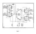
- FIG. 4illustrates a block diagram for one embodiment of a memory module 100 .
- Memory module 100contains three functional blocks; a module controller 110 ; a data interface circuit 120 ; and a memory device array 140 / 142 .
- the module controller 110synchronizes the operation of module 100 with the attached memory system. Like the address/command registers and PLL of a registered DIMM, controller 110 can provide clock adjustment to an input CLK signal and registered versions of address and command signals, RADD/RCMD. In addition, module controller 110 provides timing and synchronization signals to data interface circuit 120 . The function of the various timing and synchronization signals shown in FIG. 4 will be explained shortly.
- Data interface circuit 120provides for m-bit-wide data transfers between the module and the system memory data bus, and for R ⁇ m -bit-wide data transfers between the interface circuit and the memory device array.
- R2
- the memory device arraycomprises two memory device ranks 140 and 142 , each capable of performing m-bit-wide data transfers.
- a rank of memorycomprises enough memory devices to form a data path that is m bits wide.
- multiple rankswill receive the same address and commands, and will perform memory operations with the interface circuit concurrently.
- a bi-directional buffer 122is coupled to a bi-directional module data port that can be connected to a system memory data bus.
- An m-bit-wide path through buffer 122receives and drives data signals DQ on the system memory data bus.
- a set of data mask bits DMcan be accepted at the data port and redriven towards the memory array.
- the data mask bitsallow the memory controller to selectively write a subset of an m-bit-wide set of data signals. For instance, with a 64-bit word size, an eight-bit mask DM can be used to specify that any combination of the eight bytes making up the word should not, be written to memory.
- a data strobe signal DQScan be driven by buffer 122 onto the memory data bus.
- Two bi-directional data registers 126 and 128connect, respectively, to memory device array ranks 140 and 142 .
- Each data registercan receive an m-bit-wide word from its corresponding memory device rank, or drive an m-bit-wide word to that rank, over a dedicated point-to-point module data bus.
- each data registercan also drive a registered data-mask signal (e.g., RDM 0 for register 126 ) to its corresponding rank when the register data is written to memory.
- Multiplexer/demultiplexer (MUX/DeMUX) 124has a multiplexing ratio R.
- Rmultiplexing ratio
- either data signals DQ 0 (from register 126 ) or data signals DQ 1 (from register 128 )can be multiplexed to buffer 122 when the module is reading from memory device array 140 / 142 .
- data signals MDQ from buffer 122can be channeled to either DQ 0 or DQ 1 .
- Module controller 110synchronizes the operation of the data port buffer 122 , MUX/DeMUX 124 , and data registers 126 and 128 via a number of control signals. For instance, direction signal DIR specifies whether data flow is towards the memory array (TO) or away from the memory array (AWAY). Module controller 110 determines the current value for DIR by snooping CMD signals as they pass through controller 110 . For instance, DIR can default to TO, and switch to AWAY when the command signals latched into RCMD indicate an impending READ operation.
- direction signal DIRspecifies whether data flow is towards the memory array (TO) or away from the memory array (AWAY).
- Module controller 110determines the current value for DIR by snooping CMD signals as they pass through controller 110 . For instance, DIR can default to TO, and switch to AWAY when the command signals latched into RCMD indicate an impending READ operation.
- buffer 122When DIR is set to TO, buffer 122 is configured as a receiver (viewed looking in to circuit 120 ), MUX/DeMUX 124 is configured as a DEMUX, and registers 126 and 128 are configured as drivers (viewed looking in to circuit 120 ).
- buffer 122When DIR is set to AWAY, buffer 122 is configured as a driver, MUX/DeMUX 124 is configured as a MUX, and registers 126 and 128 are configured as receivers.
- the register select signal REG_SELdetermines whether DQ 0 or DQ 1 will be supplied to buffer 122 .
- Datais serialized from the data registers onto the memory data bus by reading 2 m bits into the data registers during one memory device read cycle, and then driving these bits, m at a time, through MUX 124 .
- REG_SELcan first select, e.g., DQ 0 during a first bus clock cycle, and then DQ 1 during the following bus clock cycle.
- register data strobe RDQSis functional. When RDQS transitions, buffer 122 latches data from MUX 124 and drives that data onto the memory data bus.
- REG_SELdetermines which of registers 126 and 128 will receive DQ at each memory bus clock cycle (note that an alternative is to supply DQ to the inputs of both registers, and ignore REG_SEL).
- register data strobes RDQS 0 and RDQS 1are also functional.
- register 126latches data from DQ 0 (and DM 0 ).
- register 128latches data from DQ 1 (and DM 1 ).
- m bitsare directed to register 126 by strobing RDQS 0 .
- m bitsare directed to register 128 by strobing RDQS 1 . Both register contents are then written to memory device array 140 / 142 during a single device write cycle. Controller 110 strobes the memory device array, using the memory data strobe MDQS, to signal the array to write data from buses RDQ 0 and RDQ 1 .
- FIG. 5illustrates a timing diagram for two consecutive read operations (to the same ROW of the memory devices) on module 100 of FIG. 4 .
- a primary memory controllerinitiates READ operations just like it would for a registered DIMM (see the description accompanying FIG. 3 ).
- controller 110latches an active command into RCMD, it enters an ACTIVE state itself.
- controller 110scans the command bus for READ or WRITE commands, as these commands signal that controller 110 will need to synchronize a data transfer.
- a READ command(to COL a) is clocked in, causing the controller to enter a READ state.
- a second READ command(to COL b) is clocked in; controller 110 counts the number of pending READ operations (including each operation's burst length if the devices support burst mode access) in order to track how long to stay in the READ state.
- Controller 110asserts DIR (where asserted equals AWAY) sometime after passing the first READ command to device array 140 / 142 .
- This assertion timecan vary, but preferably occurs prior to when device array 140 / 142 is expected to begin driving buses RDQ 0 and RDQ 1 .
- Device array 140 / 142signifies that it is about to drive data onto buses RDQ 0 and RDQ 1 by taking data strobe MDQS low at T 6 n.
- MDQSwill comprise multiple strobes, each device in device array 140 / 142 supplying at least one strobe synchronized to its data signals.
- Module controller 110senses the transition on MDQS—this causes module controller 110 to take register data strobe RDQS low in turn, thereby signaling to the primary memory controller that data transfer is about to occur.
- device array 140 / 142takes MDQS high, signifying that data outputs “DO_a 1 ” and “DO_a 2 ” are being driven respectively onto buses RDQ 0 and RDQ 1 at that time.
- Delay element 134delays MDQS long enough for the buses to settle, and then passes the MDQS strobe to registers 126 and 128 .
- registers 126 and 128latch DO_a 1 and DO_a 2 (note that with multiple strobes coming from multiple devices, each strobe may be used to latch the data signals coming from its device). Note that DQ 0 and DQ 1 contain valid data shortly after the data first appears on RDQ 0 and RDQ 1 .
- Controller 110also receives strobe MDQS.
- the positive transition of MDQStriggers two controller signals: a delayed (to correspond approximately with the appearance of valid data on DQ 0 and DQ 1 ) positive transition on strobe RDQS; and a corresponding negative transition on REG_SEL to steer DO_a 1 to buffer 122 .
- the multiplexer output trace MDQshows that concurrent with the transition of REG_SEL, DO_a 1 begins to stabilize at the input to buffer 122 , and is stable before T 8 .
- RDQSalong with the contents of DQ 0 , are latched into register 122 based on the transition of RDQS.
- a delay element 132is used to ensure that RDQS has settled at the input of buffer 122 before it is latched. Shortly before T 8 , MDQ and RDQS are latched into buffer 122 , and appear at the memory bus port as DQ and DQS shortly after T 8 .
- controller 110transitions these signals again to place DO_a 2 on the memory bus. While DO_a 2 is being latched into buffer 122 (at T 8 n), the memory devices begin data output of the results of the second READ operation. The results of the second read operation propagate through the interface circuit in similar fashion to the results of the first read operation. The net result is that the memory data bus transfers 4 m bits of data in two memory bus clock cycles (four m-bit transfers), with only two data accesses performed at each memory device on the module.
- FIG. 6shows an analogous timing diagram for two consecutive write operations.
- module controller 110enters an ACTIVE state upon latching the ACTIVE command from the primary memory controller.
- module controller 110transitions to a WRITE state. This includes taking RDQS 0 (and RDQS 1 , if desired) low in preparation for the first write operation.
- DQSis center-aligned with the write data placed on DQ by the primary memory controller. Accordingly, DQS is used to clock DQ (and DM) into buffer 122 when DQS transitions at T 5 . Between T 5 and T 5 n, DI_a 1 is valid on MDQ, as well as on DQ 0 and DQ 1 (DeMUX 124 merely passes MDQ to the inputs of both data registers in this example).
- Module controller 110also receives DQS. After a delay to allow the inputs to register 126 to settle, module controller 110 transitions RDQS 0 to latch DI_a 1 into register 126 .
- the primary memory controllertransitions DQS again, causing buffer 122 to latch DI_a 2 .
- module controller 10transitions RDQS 1 to latch DI_a 2 into register 128 .
- register 126may have separate input and output stages—this allows register 126 to hold its output long enough to ensure that the memory device array receives it, while at the same time allowing register 126 to latch the next input from DQ.
- RDQS 1can be used as a transfer signal to cause register 126 to transfer the contents of its input stage to its output stage.
- this method of operationis illustrated by the two separate traces RDQ 0 _IN (input stage) and RDQ 0 _OUT (output stage).
- FIG. 7shows the general component arrangement for a memory module 100 in a DIMM form factor.
- Two ranks of memory devicesare arranged along the top of the DIMM card: memory devices 140 A- 140 H are arranged on the facing side of the module, with memory devices 142 A- 142 H arranged directly behind these (see the side view of module 100 A in FIG. 8 ).
- Interface circuit 120 of FIG. 4is split into two identical interface circuits (left circuit 125 and right circuit 130 ) in FIG. 7, each handling half of the data lines. This arrangement allows for more uniform lead lengths between an interface circuit and each of the memory devices, and reduces the pin count on each interface circuit package.
- FIG. 4shows the general component arrangement for a memory module 100 in a DIMM form factor.
- Module controller 110is centered below the memory modules, equalizing signal distance to interface circuits 125 and 130 . This arrangement also provides a more uniform path length for address and command signals RADD/RCMD.
- the signals labeled “SYNC”include the signals DQS, RDQS, DIR, REG_SEL, RDQS 0 , and RDQS 1 shown in FIG. 4 .
- FIG. 8shows three of the modules depicted in FIG. 7 arranged in a memory system with a primary memory controller 20 and a multi-drop memory bus 22 . Note that with multiple modules, each module will recognize ACTIVE commands addressed to that module and respond accordingly; otherwise, the modules remain in a standby mode and need not pass commands through to their memory device arrays.
- FIG. 9illustrates an alternate interface circuit configuration 170 useful with a point-to-point memory data bus. Most of interface circuit directly corresponds to interface circuit 120 (MUX/DeMUX 176 and everything to the right of it). But the data port buffer in FIG. 9 is a dual-port data buffer, with a forwarding buffer 174 and a transfer buffer 172 .
- a forwarding portcomprises data signal lines FDQ, data masking signal lines FDM, and data signal strobe lines FDQS.
- the forwarding portallows for communication between the memory module and another memory module on an additional memory bus segment.
- transfers between the memory module and the primary memory controllerfunction similarly to those described for FIG. 4 . But when a set of data signals is received at the forwarding port, those signals are clocked in and then clocked out on the transfer port during the next bus clock cycle. And when a set of data signals is received at the transfer port while the memory module is not ACTIVE, those signals are clocked in and then clocked out on the forwarding port during the next bus clock cycle.
- FIG. 10shows the general component arrangement for a memory module 150 arranged in a DIMM form factor and employing the interface circuit layout of interface circuit 170 .
- the general arrangement of module 150is similar to that of module 100 of FIG. 7, with interface circuit 170 split into two halves 175 and 180 .
- the number of memory data bus connections along the card edgehas been doubled to facilitate support for a transfer port and a forwarding port.
- two address and command ports to module controller 160are also shown—one port accepts transfer address and commands (TADD/TCMD) from an attached memory controller, and the other port transmits forwarded address and commands (FADD/FCMD) to other downstream modules.
- TADD/TCMDtransfer address and commands
- FADD/FCMDforwarded address and commands
- FIG. 11shows three of the modules depicted in FIG. 10 arranged in a memory system with a primary memory controller 200 and a point-to-point memory bus 202 .
- This memory busis described as a “virtual multi-drop” bus because of its linear arrangement of modules—but the memory bus is actually made up of point-to-point data bus segments 202 A, 202 B, and 202 C.
- Data bus segment 202 Aconnects memory controller 200 to the transfer port of module 150 A.
- Data bus segment 202 Bconnects the forwarding port of module 150 A to the transfer port of module 150 B.
- data bus segment 202 Cconnects the forwarding port of module 150 B to the transfer port of module 150 C.
- module 150 Afor instance, remains in a TRANSFER mode when it is not ACTIVE. In the transfer mode, module 150 A merely picks up signals from either of its two ports and drives those signals to the other port.
- FIGS. 12 and 13illustrate a variation on the point-to-point configuration of FIGS. 10 and 11.
- memory bus 252is a ring memory bus. Like memory bus 202 , memory bus 252 contains A, B, and C segments. But in addition, memory bus 252 contains a fourth segment 252 D that connects the last module, 210 C, back to the memory controller 250 . When transfers occur on bus 252 , half of the signals are sent in a clockwise direction and the other half are sent in a counter-clockwise direction. Like in the case above, modules that are not ACTIVE remain in a TRANSFER mode in which they propagate signals along the bus. But the ACTIVE module will receive data at both of its ports, and then must combine the data to form a full data word.
- each transfer/forwarding data port(e.g., port T/FDQ 0 ) is only m/4 bits wide, whereas the ports in FIG. 10 were each m/2 bits wide.
- the ring bus architectureis one way in which an effective bit width can be different than the number of physical lines on any given memory bus segment.
- FIG. 12An issue with the configuration of FIG. 12 is that data from two ports will need to be merged at some point. From FIG. 13, it can be seen that depending on which module is active, half of the data will take longer to reach the module than the other half. This can be compensated for in several ways.
- memory controller 250can stagger transmission on segments 252 A and 252 D such that the two halves arrive at the destination module at approximately the same time.
- the interface circuitcan include a multistage buffer that delays the data input on one module port in order to align it with the data input on the other module port.
- data from each of the two portscan be written separately to memory when it arrives by splitting each rank of memory in half and delaying the address and command signals to each half by an amount that compensates for the arrival delay of the data.
- the illustrated examplesuse source-synchronous strobe signals to clock data, common-clock signaling can also be used in some embodiments and/or on some data paths of an embodiment.
- the illustrated examplesalso show two ranks of memory, but other numbers of ranks are also possible, e.g., a 4:1 multiplexer and four ranks of memory.
- the terms “buffer” and “register”have been used herein somewhat interchangeably—a register has a latching capability, whereas a buffer may have, but need not necessarily have, such a capability.
- bi-directional registers/buffers and a combination multiplexer/demultiplexerare illustrated, those skilled in the art recognize that an embodiment of the invention can also be constructed using two data paths with unidirectional components.
- DRAMdynamic random access memory
- SDRAMsynchronous DRAM
- DDRdouble-data-rate SDRAM devices
- QDRquad-data-rate SDRAM devices
- RambusTM DRAM devicesRambusTM DRAM devices (with an-appropriate controller)
- static RAMflash memory devices
Landscapes
- Engineering & Computer Science (AREA)
- Theoretical Computer Science (AREA)
- Physics & Mathematics (AREA)
- General Engineering & Computer Science (AREA)
- General Physics & Mathematics (AREA)
- Dram (AREA)
Abstract
Description
This present invention relates generally to digital memory devices and systems, and more particularly to memory module architectures and methods for operating such devices and systems.
Microprocessors, digital signal processors, video devices, and many other types of digital data processing devices rely on an attached high-speed memory system to hold data and/or processor instructions needed by the processing device. As these processing devices become faster and more powerful, the increased demands placed on them generally translates to a need for larger and faster attached memory systems.
FIG. 1 depicts a typical memory system configuration. One or more memory devices26AA,26AB,26BA,26BB,26CA, and26CB interface with amemory controller 20 throughmemory bus 22. A host (e.g., a central processing unit (CPU), not shown) also connects tomemory controller 20 through a front-side bus FSB. The memory devices hold data in arrays of addressable memory cells.Memory controller 20 controls the exchange of data between the host and the memory storage devices.
In the configuration shown in FIG. 1,memory bus 22 is a multi-drop memory bus. In other words,bus 22 is arranged with a backbone of signal lines. A signal line stub, or “drop”, connects each of the memory devices (e.g.,26A) to the backbone. Typically,memory bus 22 will comprise a collection of leads routed on a printedcircuit board 21 known as the “main board” or “motherboard”.Memory controller 20 mounts tomotherboard 21 and connects to one end of the leads comprisingmemory bus 22. Each drop ofmemory bus 22 connects to an electrical terminator, or socket. A typical main board contains multiple memory sockets, e.g., the threesockets
Memory is added to the memory system by inserting memory modules (e.g.,24A,24B,24C) into one or more of the sockets. One popular type of memory module is a Dual In-line Memory Module, or DIMM. The DIMM is a rectangular low-profile circuit board that has electrical contact points arranged on both sides along one long edge. The contact points form electrical connections to the main board's memory bus when the DIMM is inserted into a DIMM memory socket.
A DIMM generally has multiple individual memory devices mounted to it. The devices all work in parallel to perform memory functions. For instance, a DIMM may have eight memory devices, each of which receives the same memory address from the controller. If the size of a data word is 32 bits, each of the memory devices is responsible for four bits of the data word that is placed on the memory bus.
Some DIMM designs (like the design shown in FIG. 1) have more than one bank of memory devices. For example, FIG. 2 shows a block diagram of a registeredDIMM 24 containing eighteen memory devices arranged in two banks, one bank containing devices D00-D08 and the other containing devices D10-D18. In a registered DIMM, the system clock CK0 is received by phase-locked-loop (PLL)27, which creates a set of module clock signals. Address and command signals ADD/CMD are latched into aregister 25 at the edge of one clock cycle, and then redriven onto the module addressing/command bus as register signals RADD/RCMD on the following clock cycle. Note that two bank select signals, B0_SEL# and B1_SEL#, each pass throughregister 25 and connect to a chip select pin on a corresponding one of the banks of memory devices. The data lines DQ of the memory device banks each connect to the memory bus of the host system. A total of nB DQ lines carry data signals, where B is the number of devices in one bank (e.g., eight or nine), and n is the data width of each device (e.g., four, eight, or sixteen bits). In addition, B DQS lines carry data strobes (one per device). The DQS data strobes travel with the data signals, and can be used for source-synchronous clocking of the data signals at the receiver.
FIG. 3 shows a timing diagram for two consecutive random reads to memory bank D00-D08. At TI, the memory controller transmits an ACTIVE command along with a ROW address, and takes B0_SEL# low to select bank0 onmodule 24. Register25 latches these signals, and places them on the module bus at T2. After a known RAS (row address strobe) latency, the controller transmits a READ command along with a COL “a” address. These signals also pass throughregister 25 with a one-clock cycle delay. After a known CAS (column address strobe) latency, the memory bank places data (DO a) from ROW and COL “a” onto bus lines DQ, and DQS is driven as well. Note that a read to a COL “b” can immediately follow the first read, as the columns are on the same ROW.
The invention may be best understood by reading the disclosure with reference to the drawing, wherein:
FIG. 1 illustrates an edge view of a prior art memory system;
FIG. 2 contains a block diagram a prior art registered DIMM;
FIG. 3 shows a timing diagram for two consecutive read operations for the registered DIMM of FIG. 2;
FIG. 4 shows a block diagram for a memory module according to one embodiment of the invention;
FIG. 5 shows a timing diagram for two consecutive read operations for the memory a module of FIG. 4;
FIG. 6 shows a timing diagram for two consecutive write operations for the memory module of FIG. 4;
FIGS. 7 and 8 shows, respectively, a side view for a general DIMM module layout for the memory module of FIG. 4, and a side edge view of multiple DIMM modules of this type connected to a multi-drop memory bus;
FIG. 9 shows a block diagram for a memory module interface circuit useful with another embodiment of the invention;
FIGS. 10 and 11 show, respectively, a side view for a general DIMM module layout for the memory module using the interface circuit of FIG. 9, and a side edge view of multiple DIMM modules of this type connected to a point-to-point virtual multi-drop memory bus; and
FIGS. 12 and 13 show, respectively, a side view for a general DIMM module layout using a variation of the interface circuit of FIG. 9, and a side edge view of multiple DIMM modules of this type connected to a point-to-point ring memory bus.
The dual-bank registered DIMM design of FIG. 2 has at least one desirable characteristic when compared to a single-bank design—for a given memory capacity on each device and a fixed memory bus width, the dual-bank design allows the capacity of the DIMM to double. A dual-bank DIMM can generally be manufactured for less than twice the cost of a single-bank DIMM and is therefore cheaper than two single-bank DIMMs. Dual-bank DIMMs can also be desirable where the number of DIMM sockets on a motherboard is limited.
The present disclosure includes a group of buffered memory module architectures. Generally, the disclosed embodiments use a memory module interface circuit that, in essence, widens the data bus on the memory module as compared to the width of the system memory data bus, allowing a faster system memory data bus to operate at full speed with slower memory devices. Preferably, this characteristic of the module is transparent to the memory system and to the memory devices: to the memory system, it appears that the module comprises memory devices that operate at the full speed of the memory system data bus; to the memory devices, it appears that each is connected to a controller operating at a slower speed compatible with the devices. This allows for an embodiment that is compatible with an existing memory controller/bus and with existing memory devices.
The memory module configurations and access methods disclosed herein can improve on the dual-bank registered DIMM in several respects. For instance, one embodiment describes a DIMM that can, with the same type of devices, number of devices, and data signal pins as the dual-bank registered DIMM, provide twice the data rate of the registered DIMM. This configuration can also allow the memory devices to operate at voltage levels independent of the voltage levels of the memory system that the module is attached to. The exemplary embodiments also allow the memory devices to be isolated from the full capacitive loading effects of the system memory data bus. Further, the memory devices of the embodiments avoid arrangements of competing memory banks that load each other, as is the case with a dual-bank DIMM. Finally, with the disclosed embodiments there is less need for complex logic, within the memory devices themselves, in order to increase the bandwidth of the memory system.
It is recognized herein that the multi-drop memory bus architecture also has several characteristics that limit its expansion to greater numbers of memory devices and/or faster bus speeds. First, the stubbed bus architecture can create undesirable reflections on the signal lines at high frequency. Overall bus length can also cause timing problems that limit operational frequency, as at high frequency a significant skew will be observed between when a memory signal arrives at a closer device vs. when that signal arrives at a device further down the bus. The length of the bus and the number of device inputs also determine the capacitance that a memory device (or the controller) sees when it drives the bus—at higher frequencies, this capacitance may make it infeasible to drive signals reliably on the bus.
The memory systems and modules described herein generally improve upon the multi-drop memory bus architecture by isolating the memory devices on each module from the bus, while providing retiming at the interface circuit of each module. Some of the disclosed embodiments go even further, by adding a dual port buffer to the module data port of the interface circuit. The dual-port buffer allows a primary memory controller and the modules to be connected in a point-to-point architecture. In this architecture, each memory module communicates directly with only its two nearest neighbors. Memory signals are forwarded from module to module until they reach the controller or the module that they are addressed to.
FIG. 4 illustrates a block diagram for one embodiment of amemory module 100.Memory module 100 contains three functional blocks; amodule controller 110; adata interface circuit 120; and amemory device array 140/142.
Themodule controller 110 synchronizes the operation ofmodule 100 with the attached memory system. Like the address/command registers and PLL of a registered DIMM,controller 110 can provide clock adjustment to an input CLK signal and registered versions of address and command signals, RADD/RCMD. In addition,module controller 110 provides timing and synchronization signals todata interface circuit 120. The function of the various timing and synchronization signals shown in FIG. 4 will be explained shortly.
In FIG. 4, abi-directional buffer 122 is coupled to a bi-directional module data port that can be connected to a system memory data bus. An m-bit-wide path throughbuffer 122 receives and drives data signals DQ on the system memory data bus. Optionally, a set of data mask bits DM can be accepted at the data port and redriven towards the memory array. The data mask bits allow the memory controller to selectively write a subset of an m-bit-wide set of data signals. For instance, with a 64-bit word size, an eight-bit mask DM can be used to specify that any combination of the eight bytes making up the word should not, be written to memory. Finally, a data strobe signal DQS can be driven bybuffer 122 onto the memory data bus.
Two bi-directional data registers126 and128 connect, respectively, to memory device array ranks140 and142. Each data register can receive an m-bit-wide word from its corresponding memory device rank, or drive an m-bit-wide word to that rank, over a dedicated point-to-point module data bus. When the optional data-masking signal feature is implemented, each data register can also drive a registered data-mask signal (e.g., RDM0 for register126) to its corresponding rank when the register data is written to memory.
Multiplexer/demultiplexer (MUX/DeMUX)124 has a multiplexing ratio R. In FIG. 4, either data signals DQ0 (from register126) or data signals DQ1 (from register128) can be multiplexed to buffer122 when the module is reading frommemory device array 140/142. If Likewise, when the module is writing to the memory device array, data signals MDQ frombuffer 122 can be channeled to either DQ0 or DQ1.
The register select signal REG_SEL, in the AWAY mode, determines whether DQ0 or DQ1 will be supplied to buffer122. Data is serialized from the data registers onto the memory data bus by reading 2 m bits into the data registers during one memory device read cycle, and then driving these bits, m at a time, through MUX124. For instance, REG_SEL can first select, e.g., DQ0 during a first bus clock cycle, and then DQ1 during the following bus clock cycle. In the AWAY mode, register data strobe RDQS is functional. When RDQS transitions, buffer122 latches data from MUX124 and drives that data onto the memory data bus.
In the TO mode, REG_SEL determines which ofregisters memory device array 140/142 during a single device write cycle.Controller 110 strobes the memory device array, using the memory data strobe MDQS, to signal the array to write data from buses RDQ0 and RDQ1.
FIG. 5 illustrates a timing diagram for two consecutive read operations (to the same ROW of the memory devices) onmodule 100 of FIG.4. Externally, a primary memory controller initiates READ operations just like it would for a registered DIMM (see the description accompanying FIG.3). Whencontroller 110 latches an active command into RCMD, it enters an ACTIVE state itself. In the ACTIVE state,controller 110 scans the command bus for READ or WRITE commands, as these commands signal thatcontroller 110 will need to synchronize a data transfer. At T4, a READ command (to COL a) is clocked in, causing the controller to enter a READ state. At T5, a second READ command (to COL b) is clocked in;controller 110 counts the number of pending READ operations (including each operation's burst length if the devices support burst mode access) in order to track how long to stay in the READ state.
At T7n,device array 140/142 takes MDQS high, signifying that data outputs “DO_a1” and “DO_a2” are being driven respectively onto buses RDQ0 and RDQ1 at that time.Delay element 134 delays MDQS long enough for the buses to settle, and then passes the MDQS strobe toregisters
RDQS, along with the contents of DQ0, are latched intoregister 122 based on the transition of RDQS. Adelay element 132 is used to ensure that RDQS has settled at the input ofbuffer 122 before it is latched. Shortly before T8, MDQ and RDQS are latched intobuffer 122, and appear at the memory bus port as DQ and DQS shortly after T8.
Approximately a half-clock cycle after transitioning RDQS and REG_SEL,controller 110 transitions these signals again to place DO_a2 on the memory bus. While DO_a2 is being latched into buffer122 (at T8n), the memory devices begin data output of the results of the second READ operation. The results of the second read operation propagate through the interface circuit in similar fashion to the results of the first read operation. The net result is that the memory data bus transfers4m bits of data in two memory bus clock cycles (four m-bit transfers), with only two data accesses performed at each memory device on the module.
FIG. 6 shows an analogous timing diagram for two consecutive write operations. Like in the case above,module controller 110 enters an ACTIVE state upon latching the ACTIVE command from the primary memory controller. Upon sensing the first WRITE command,module controller 110 transitions to a WRITE state. This includes taking RDQS0 (and RDQS1, if desired) low in preparation for the first write operation.
DQS is center-aligned with the write data placed on DQ by the primary memory controller. Accordingly, DQS is used to clock DQ (and DM) intobuffer 122 when DQS transitions at T5. Between T5 and T5n, DI_a1 is valid on MDQ, as well as on DQ0 and DQ1 (DeMUX124 merely passes MDQ to the inputs of both data registers in this example).
At T5n, the primary memory controller transitions DQS again, causingbuffer 122 to latch DI_a2. After a delay to allow the inputs to register128 to settle, module controller10 transitions RDQS1 to latch DI_a2 intoregister 128.
Note that in some embodiments, register126 may have separate input and output stages—this allows register126 to hold its output long enough to ensure that the memory device array receives it, while at the sametime allowing register 126 to latch the next input from DQ. When such an arrangement is used, RDQS1 can be used as a transfer signal to causeregister 126 to transfer the contents of its input stage to its output stage. In FIG. 6, this method of operation is illustrated by the two separate traces RDQ0_IN (input stage) and RDQ0_OUT (output stage).
FIG. 7 shows the general component arrangement for amemory module 100 in a DIMM form factor. Two ranks of memory devices are arranged along the top of the DIMM card:memory devices 140A-140H are arranged on the facing side of the module, withmemory devices 142A-142H arranged directly behind these (see the side view ofmodule 100A in FIG.8).Interface circuit 120 of FIG. 4 is split into two identical interface circuits (left circuit125 and right circuit130) in FIG. 7, each handling half of the data lines. This arrangement allows for more uniform lead lengths between an interface circuit and each of the memory devices, and reduces the pin count on each interface circuit package. In FIG. 7, the data signal lines for one memory rank are arranged on the front side of the card (solid lines leading to the memory devices), and the data signal lines for the other memory rank are arranged on the back side of the card (dashed lines leading to the memory devices).Module controller 110 is centered below the memory modules, equalizing signal distance to interfacecircuits 125 and130. This arrangement also provides a more uniform path length for address and command signals RADD/RCMD. The signals labeled “SYNC” include the signals DQS, RDQS, DIR, REG_SEL, RDQS0, and RDQS1 shown in FIG.4.
FIG. 8 shows three of the modules depicted in FIG. 7 arranged in a memory system with aprimary memory controller 20 and amulti-drop memory bus 22. Note that with multiple modules, each module will recognize ACTIVE commands addressed to that module and respond accordingly; otherwise, the modules remain in a standby mode and need not pass commands through to their memory device arrays.
FIG. 9 illustrates an alternateinterface circuit configuration 170 useful with a point-to-point memory data bus. Most of interface circuit directly corresponds to interface circuit120 (MUX/DeMUX 176 and everything to the right of it). But the data port buffer in FIG. 9 is a dual-port data buffer, with a forwardingbuffer 174 and atransfer buffer 172.
Communication between the primary memory controller and the interface take place at the transfer port, which comprises data signal lines TDQ, data masking signal lines TDM, and data signal strobe lines TDQS. A forwarding port comprises data signal lines FDQ, data masking signal lines FDM, and data signal strobe lines FDQS. The forwarding port allows for communication between the memory module and another memory module on an additional memory bus segment.
In operation, transfers between the memory module and the primary memory controller function similarly to those described for FIG.4. But when a set of data signals is received at the forwarding port, those signals are clocked in and then clocked out on the transfer port during the next bus clock cycle. And when a set of data signals is received at the transfer port while the memory module is not ACTIVE, those signals are clocked in and then clocked out on the forwarding port during the next bus clock cycle.
FIG. 10 shows the general component arrangement for amemory module 150 arranged in a DIMM form factor and employing the interface circuit layout ofinterface circuit 170. The general arrangement ofmodule 150 is similar to that ofmodule 100 of FIG. 7, withinterface circuit 170 split into twohalves 175 and180. The number of memory data bus connections along the card edge, however, has been doubled to facilitate support for a transfer port and a forwarding port. Note also that two address and command ports tomodule controller 160 are also shown—one port accepts transfer address and commands (TADD/TCMD) from an attached memory controller, and the other port transmits forwarded address and commands (FADD/FCMD) to other downstream modules.
FIG. 11 shows three of the modules depicted in FIG. 10 arranged in a memory system with aprimary memory controller 200 and a point-to-point memory bus202. This memory bus is described as a “virtual multi-drop” bus because of its linear arrangement of modules—but the memory bus is actually made up of point-to-pointdata bus segments Data bus segment 202A connectsmemory controller 200 to the transfer port ofmodule 150A.Data bus segment 202B connects the forwarding port ofmodule 150A to the transfer port ofmodule 150B. Anddata bus segment 202C connects the forwarding port ofmodule 150B to the transfer port ofmodule 150C. In operation,module 150A, for instance, remains in a TRANSFER mode when it is not ACTIVE. In the transfer mode,module 150A merely picks up signals from either of its two ports and drives those signals to the other port.
FIGS. 12 and 13 illustrate a variation on the point-to-point configuration of FIGS. 10 and 11. In FIG. 13,memory bus 252 is a ring memory bus. Like memory bus202,memory bus 252 contains A, B, and C segments. But in addition,memory bus 252 contains afourth segment 252D that connects the last module,210C, back to thememory controller 250. When transfers occur onbus 252, half of the signals are sent in a clockwise direction and the other half are sent in a counter-clockwise direction. Like in the case above, modules that are not ACTIVE remain in a TRANSFER mode in which they propagate signals along the bus. But the ACTIVE module will receive data at both of its ports, and then must combine the data to form a full data word.
An advantage of the ring bus architecture is that is allows point-to-point bus connections without doubling the number of card pins. Referring to FIG. 12, each transfer/forwarding data port (e.g., port T/FDQ0) is only m/4 bits wide, whereas the ports in FIG. 10 were each m/2 bits wide. The ring bus architecture is one way in which an effective bit width can be different than the number of physical lines on any given memory bus segment.
An issue with the configuration of FIG. 12 is that data from two ports will need to be merged at some point. From FIG. 13, it can be seen that depending on which module is active, half of the data will take longer to reach the module than the other half. This can be compensated for in several ways. First,memory controller 250 can stagger transmission onsegments
Many other variations on the illustrated embodiments are possible. For instance, although the illustrated examples use source-synchronous strobe signals to clock data, common-clock signaling can also be used in some embodiments and/or on some data paths of an embodiment. The illustrated examples also show two ranks of memory, but other numbers of ranks are also possible, e.g., a 4:1 multiplexer and four ranks of memory. The terms “buffer” and “register” have been used herein somewhat interchangeably—a register has a latching capability, whereas a buffer may have, but need not necessarily have, such a capability. Although bi-directional registers/buffers and a combination multiplexer/demultiplexer are illustrated, those skilled in the art recognize that an embodiment of the invention can also be constructed using two data paths with unidirectional components.
An embodiment can also have the capability to respond to a read that requests less than N=R×m bits by transferring less than N bits on the memory bus. For instance, consider a case where m=16 and R=4. If an allowable read operation requests only one 16-bit word, the module can respond by performing one 64-bit read internally to the four data registers. Then, only the one register of the four that contains the requested 16-bit word is multiplexed onto the memory data bus. This can be extended to read any number of m-bit words from one to R.
Likewise, an embodiment can also have the capability to respond to a write that requests to write less than N=R×m bits. Using the example above, if an allowable write operation requests to write only one 16-bit word, the masking bits on the other words can be set by the controller. The when a write to the ranks is performed, only the one word requested by the external memory controller will actually be written, and the other three words stored in the data registers will be ignored.
The types, sizes, or numbers of memory devices selected for use with the present invention are not critical. Some possible device types include dynamic random access memory (DRAM) devices, synchronous DRAM (SDRAM) devices including double-data-rate (DDR) SDRAM devices, quad-data-rate (QDR) SDRAM devices, Rambus™ DRAM devices (with an-appropriate controller), static RAM and flash memory devices. It may be possible to combine memory modules in a memory system according to the invention where two modules incorporate different types of memory devices.
One of ordinary skill in the art will recognize that the concepts taught herein can be tailored to a particular application in many other advantageous ways. For instance, although the illustrated embodiments use one or two interface circuits and a separate module controller, all of these devices could be integrated in a single device, or in some other number of packages with some other division of the tasks to be performed by the module. The ranks need not be arranged on opposite sides of a card. Such minor modifications are encompassed within the invention, and are intended to fall within the scope of the claims. Although the specification may refer to “an”, “one”, “another”, or “some” embodiment(s) in several locations, this does not necessarily mean that each such reference is to the same embodiment(s), or that the feature only applies to a single embodiment.
Claims (20)
1. A memory system comprising:
a primary memory controller;
a memory data bus, having an effective bit-width m, coupled to the primary memory controller; and
at least one memory module coupled to the memory data bus, the memory module having a module data bus with an effective bit-width N=R×m, where R is an integer value greater than one, the memory module comprising an interface circuit coupled between the memory data bus and the module data bus, the interface circuit capable of performing m-bit-wide data transfers on the memory data bus, the interface circuit capable of performing N-bit-wide data transfers on the module data bus,
the memory data bus comprising a point-to-point bus having one data bus segment connecting the primary memory controller and the first of the at least one memory modules, and one additional segment for each additional memory module, the additional segment connecting the additional memory module to the module immediately preceding it, and a ring data bus segment connecting the last of the memory modules in the memory system.
2. The memory system ofclaim 1 , wherein the memory data bus and the module data bus each have a clock rate, the memory data bus clocking at a rate R times the clock rate of the module data bus.
3. A memory module comprising:
R ranks of memory devices, where R is at least two, each rank having an m-bit-wide data port;
a module data port capable of exchanging data signaling over a memory data bus having an effective bit-width m;
an interface circuit coupled between the module data port and the R memory-device-rank data ports, the interface circuit capable of performing m-bit-wide data transfers at the module data port, the interface circuit capable of performing R×m-bit-wide data transfers with the R ranks of memory devices, the interface circuit comprising
R m-bit-wide data registers, each register capable of exchanging point-to-point data signaling with a corresponding rank of memory devices through the data port of that rank, and
a multiplexer, having a multiplexing ratio R, coupled between the R data registers and the external data port; and
a controller capable of synchronizing the operation of the interface circuit and the memory device ranks such that a data transfer comprising R serial data transfers on the memory data bus can be completed internal to the memory module with one R×m-bit-wide data transfer with the memory device ranks.
4. The memory module ofclaim 3 , wherein the controller supplies rank selection signals to the multiplexer and register latching signals to each of the data registers.
5. The memory module ofclaim 3 , wherein data signaling between a data register and its rank of memory devices further comprises a bit mask received from the memory data bus along with a corresponding m bits, the multiplexer transferring the bit mask to the data register along with the corresponding m bits.
6. The memory module ofclaim 3 , wherein the controller is capable of synchronizing the operation of the data registers, the module data port, and the multiplexer/demultiplexer in order to serialize data from a subset of the data registers onto the memory data bus.
7. The memory module ofclaim 3 , wherein data transfers between one of the data registers and the corresponding rank of memory devices occurs at a clock rate related to the clock rate of the memory data bus by a factor 1/R.
8. The memory module ofclaim 3 , where the module is a dual-inline memory module comprising a printed circuit board capable of connection to the memory data bus via insertion of the circuit board into a card edge connector connected to the memory data bus.
9. The memory module ofclaim 8 , wherein R equals two, one of the two ranks of memory devices arranged on each side of the circuit board and connected to the corresponding data register via a set of module data signaling lines routed on the circuit board.
10. The memory module ofclaim 8 , wherein the interface circuit comprises two interface circuits each serving half of the module data port and half of each rank of memory devices.
11. The memory module ofclaim 3 , wherein the module data port comprises a dual-port buffer, each port of the dual-port buffer capable of connection to another memory module in a point-to-point configuration of memory data bus segments.
12. The memory module ofclaim 3 , wherein data exchanges over the memory data bus comprise a data strobe signal, the module further comprising a data strobe circuit to generate data strobe signaling when transmitting data over the memory data bus.
13. The memory module ofclaim 12 , wherein the controller begins an internal sequence of interface circuit write operations in response to an externally-supplied data strobe signal.
14. The memory module ofclaim 3 , wherein data exchanges between the interface circuit and the ranks of memory devices comprise a data strobe signal, the module further comprising a data strobe circuit to generate data strobe signaling when transmitting data from the interface circuit to the ranks of memory devices, the interface circuit comprising a register circuit to latch data from the ranks of memory devices based on data strobe signaling received from those devices.
15. A memory module comprising:
R ranks of memory devices, where R is at least two, each rank having an m-bit-wide data port;
a module data port capable of exchanging data signaling over a memory data bus having an effective bit-width m;
an interface circuit coupled between the module data port and the R memory-device-rank data ports, the interface circuit capable of performing m-bit-wide data transfers at the module data port, the interface circuit capable of performing R×m-bit-wide data transfers with the R ranks of memory devices; and
a controller capable of synchronizing the operation of the interface circuit and the memory device ranks such that a data transfer comprising R serial data transfers on the memory data bus can be completed internal to the memory module with one R×m-bit-wide data transfer with the memory device ranks;
wherein the module data port comprises a dual-port buffer, each port of the dual-port buffer capable of connection to another memory module in a point-to-point configuration of memory data bus segments, wherein each port is capable of connection to an m-bit-wide memory data bus segment, wherein one port comprises a transfer port and the other port comprises a forwarding port, the module capable of using the transfer port to transfer data signals between the interface circuit and a higher-level controller connected to the memory data bus, the module capable of using the forwarding port to connect to a second memory module in order to transfer data signals between the transfer port on the first memory module and the transfer port on the second memory module.
16. A memory module comprising:
R ranks of memory devices, where R is at least two, each rank having an m-bit-wide data port;
a module data port capable of exchanging data signaling over a memory data bus having an effective bit-width m;
an interface circuit coupled between the module data port and the R memory-device-rank data ports, the interface circuit capable of performing m-bit-wide data transfers at the module data port, the interface circuit capable of performing R×m-bit-wide data transfers with the R ranks of memory devices; and
a controller capable of synchronizing the operation of the interface circuit and the memory device ranks such that a data transfer comprising R serial data transfers on the memory data bus can be completed internal to the memory module with one R×m-bit-wide data transfer with the memory device ranks,
wherein the module data port comprises a dual-port buffer, each port of the dual-port buffer capable of connection to another memory module in a point-to-point configuration of memory data bus segments, wherein each module data port is capable of connection to an m/2-bit-wide memory data bus segment, wherein the dual module data ports comprise first and second transfer/forwarding ports, the module capable of retransmitting data signals received at one of the transfer/forwarding ports, but not destined for that memory module, on the other transfer/forwarding port, the module also capable of transferring m/2 data signals between each of the transfer/forwarding ports and the interface circuit.
17. A method of host/memory communication comprising:
initiating a data access transaction, involving N data bits, between a memory controller and a memory module;
at the memory module, initiating a corresponding data access transaction between an interface circuit and R ranks of memory devices, each rank capable of m-bit-wide data transfers, R>1;
transferring the N data bits between the memory controller and the memory module in m-bit-wide data segments; and
transferring the N data bits between the interface circuit and the R ranks of memory devices in M R×m-bit-wide segments, where

is an integer value,
wherein the method further comprises initiating a valid data access transaction when N is an integer multiple of m, but less than R×m.
18. The method ofclaim 17 , further comprising clocking transfers between the memory controller and the memory module at R times the rate that transfers are clocked between the interface circuit and the memory devices.
19. The method ofclaim 17 , wherein when the data access transaction is a write transaction, transferring the N data bits between the interface circuit and N/m of the ranks of memory devices, while signaling the remainder of the ranks to ignore the write transaction.
20. The method ofclaim 17 , wherein when the data access transaction is a read transaction, transferring R×m data bits, including the N data bits requested for the read transaction, from the R ranks of memory devices to the interface circuit, and transferring the N data bits requested for the read transaction from the memory module to the memory controller.
Priority Applications (2)
| Application Number | Priority Date | Filing Date | Title |
|---|---|---|---|
| US09/678,751US6742098B1 (en) | 2000-10-03 | 2000-10-03 | Dual-port buffer-to-memory interface |
| US10/100,312US7024518B2 (en) | 1998-02-13 | 2002-03-13 | Dual-port buffer-to-memory interface |
Applications Claiming Priority (1)
| Application Number | Priority Date | Filing Date | Title |
|---|---|---|---|
| US09/678,751US6742098B1 (en) | 2000-10-03 | 2000-10-03 | Dual-port buffer-to-memory interface |
Related Parent Applications (1)
| Application Number | Title | Priority Date | Filing Date |
|---|---|---|---|
| US09/023,170Continuation-In-PartUS7007130B1 (en) | 1997-12-05 | 1998-02-13 | Memory system including a memory module having a memory module controller interfacing between a system memory controller and memory devices of the memory module |
Related Child Applications (1)
| Application Number | Title | Priority Date | Filing Date |
|---|---|---|---|
| US10/100,312Continuation-In-PartUS7024518B2 (en) | 1998-02-13 | 2002-03-13 | Dual-port buffer-to-memory interface |
Publications (1)
| Publication Number | Publication Date |
|---|---|
| US6742098B1true US6742098B1 (en) | 2004-05-25 |
Family
ID=32313315
Family Applications (1)
| Application Number | Title | Priority Date | Filing Date |
|---|---|---|---|
| US09/678,751Expired - LifetimeUS6742098B1 (en) | 1998-02-13 | 2000-10-03 | Dual-port buffer-to-memory interface |
Country Status (1)
| Country | Link |
|---|---|
| US (1) | US6742098B1 (en) |
Cited By (150)
| Publication number | Priority date | Publication date | Assignee | Title |
|---|---|---|---|---|
| US20020112119A1 (en)* | 1998-02-13 | 2002-08-15 | Intel Corporation | Dual-port buffer-to-memory interface |
| US20030053471A1 (en)* | 2001-09-19 | 2003-03-20 | Reidar Stief | Circuit configuration for receiving a data signal |
| US20030163606A1 (en)* | 2000-06-21 | 2003-08-28 | Mueo Fukaishi | High-speed memory system |
| US20030221044A1 (en)* | 2002-05-22 | 2003-11-27 | Elpida Memory, Inc. | Memory system, module and register |
| US20040044832A1 (en)* | 2002-08-27 | 2004-03-04 | Dodd James M | Precharge suggestion |
| US20040042320A1 (en)* | 2002-08-27 | 2004-03-04 | Dodd James M. | Address decode |
| US20040071040A1 (en)* | 2002-07-31 | 2004-04-15 | Seiji Funaba | Memory module and memory system |
| US20040088450A1 (en)* | 2002-10-30 | 2004-05-06 | Dodd James M. | Memory transaction ordering |
| US20040117569A1 (en)* | 2002-12-12 | 2004-06-17 | Kye-Hyun Kyung | Memory system having two-way ring topology and memory device and memory module for ring-topology memory system |
| US20040133736A1 (en)* | 2003-01-03 | 2004-07-08 | Samsung Electronics Co., Ltd. | Memory module device for use in high-frequency operation |
| US20040158677A1 (en)* | 2003-02-10 | 2004-08-12 | Dodd James M. | Buffered writes and memory page control |
| US20040221106A1 (en)* | 2001-02-28 | 2004-11-04 | Perego Richard E. | Upgradable memory system with reconfigurable interconnect |
| US6820163B1 (en)* | 2000-09-18 | 2004-11-16 | Intel Corporation | Buffering data transfer between a chipset and memory modules |
| US20040260859A1 (en)* | 2000-06-09 | 2004-12-23 | Samsung Electronics Co., Ltd. | Memory module with improved data bus performance |
| US20050010737A1 (en)* | 2000-01-05 | 2005-01-13 | Fred Ware | Configurable width buffered module having splitter elements |
| US20050071581A1 (en)* | 2003-09-30 | 2005-03-31 | Dodd James M. | Adaptive page management |
| US20050146980A1 (en)* | 2003-12-30 | 2005-07-07 | Mooney Stephen R. | Fixed phase clock and strobe signals in daisy chained chips |
| US20050157579A1 (en)* | 2002-06-26 | 2005-07-21 | Perego Richard E. | Memory device supporting a dynamically configurable core organization |
| US20050177695A1 (en)* | 2004-02-05 | 2005-08-11 | Larson Douglas A. | Apparatus and method for data bypass for a bi-directional data bus in a hub-based memory sub-system |
| US20050216677A1 (en)* | 2004-03-24 | 2005-09-29 | Jeddeloh Joseph M | Memory arbitration system and method having an arbitration packet protocol |
| US20050268059A1 (en)* | 2004-05-25 | 2005-12-01 | Laberge Paul A | On-die termination snooping for 2T applications in a dynamic random access memory device |
| US20050265108A1 (en)* | 2002-07-29 | 2005-12-01 | Samsung Electronics, Co., Ltd. | Memory controller which increases bus bandwidth, data transmission method using the same, and computer system having the same |
| US20050268060A1 (en)* | 2004-05-28 | 2005-12-01 | Cronin Jeffrey J | Method and system for terminating write commands in a hub-based memory system |
| US7007130B1 (en) | 1998-02-13 | 2006-02-28 | Intel Corporation | Memory system including a memory module having a memory module controller interfacing between a system memory controller and memory devices of the memory module |
| US20060066375A1 (en)* | 2004-04-05 | 2006-03-30 | Laberge Paul A | Delay line synchronizer apparatus and method |
| US20060117152A1 (en)* | 2004-01-05 | 2006-06-01 | Smart Modular Technologies Inc., A California Corporation | Transparent four rank memory module for standard two rank sub-systems |
| US20060117155A1 (en)* | 2004-11-29 | 2006-06-01 | Ware Frederick A | Micro-threaded memory |
| US20060136683A1 (en)* | 2003-10-20 | 2006-06-22 | Meyer James W | Arbitration system and method for memory responses in a hub-based memory system |
| US20060174070A1 (en)* | 2002-08-16 | 2006-08-03 | Jeddeloh Joseph M | Memory hub bypass circuit and method |
| US20060200602A1 (en)* | 2003-08-20 | 2006-09-07 | Ralph James | Method and system for capturing and bypassing memory transactions in a hub-based memory system |
| US20060218318A1 (en)* | 2004-03-29 | 2006-09-28 | Ralph James | Method and system for synchronizing communications links in a hub-based memory system |
| US20060215434A1 (en)* | 2003-05-08 | 2006-09-28 | Lee Terry R | Apparatus and methods for a physical layout of simultaneously sub-accessible memory modules |
| US20060227627A1 (en)* | 2005-03-03 | 2006-10-12 | Georg Braun | Buffer component for a memory module, and a memory module and a memory system having such buffer component |
| US20060236201A1 (en)* | 2003-04-14 | 2006-10-19 | Gower Kevin C | High reliability memory module with a fault tolerant address and command bus |
| US20060262586A1 (en)* | 2004-03-05 | 2006-11-23 | Solomon Jeffrey C | Memory module with a circuit providing load isolation and memory domain translation |
| US20060262632A1 (en)* | 2005-05-17 | 2006-11-23 | Intel Corporation | Identical chips with different operations in a system |
| US20070005834A1 (en)* | 2005-06-30 | 2007-01-04 | Intel Corporation | Memory chips with buffer circuitry |
| US7176714B1 (en)* | 2004-05-27 | 2007-02-13 | Altera Corporation | Multiple data rate memory interface architecture |
| US20070070669A1 (en)* | 2005-09-26 | 2007-03-29 | Rambus Inc. | Memory module including a plurality of integrated circuit memory devices and a plurality of buffer devices in a matrix topology |
| US20070091712A1 (en)* | 2005-10-26 | 2007-04-26 | Intel Corporation | Clocking architecture using a bi-directional reference clock |
| US20070147016A1 (en)* | 2005-12-23 | 2007-06-28 | Intel Corporation | Memory systems with memory chips down and up |
| US7240145B2 (en) | 1997-12-05 | 2007-07-03 | Intel Corporation | Memory module having a memory controller to interface with a system bus |
| US20070260841A1 (en)* | 2006-05-02 | 2007-11-08 | Hampel Craig E | Memory module with reduced access granularity |
| US20080031077A1 (en)* | 2006-07-26 | 2008-02-07 | Gerald Keith Bartley | Daisy chainable memory chip |
| US20080068900A1 (en)* | 2004-03-05 | 2008-03-20 | Bhakta Jayesh R | Memory module decoder |
| US20080080261A1 (en)* | 2005-09-26 | 2008-04-03 | Rambus Inc. | Memory system topologies including a buffer device and an integrated circuit memory device |
| US7386649B2 (en) | 2003-08-28 | 2008-06-10 | Micron Technology, Inc. | Multiple processor system and method including multiple memory hub modules |
| US20090103372A1 (en)* | 2007-10-19 | 2009-04-23 | Uniram Technology Inc. | High performance high capacity memory systems |
| US20090103387A1 (en)* | 2007-10-19 | 2009-04-23 | Uniram Technology Inc. | High performance high capacity memory systems |
| US20090103373A1 (en)* | 2007-10-19 | 2009-04-23 | Uniram Technology Inc. | High performance high capacity memory systems |
| US20090166574A1 (en)* | 2003-08-29 | 2009-07-02 | Shunichiro Hagihara | Receiving Opening Of Joint For Working Fluid And Valve With The Receiving Opening |
| US20090285031A1 (en)* | 2005-06-24 | 2009-11-19 | Suresh Natarajan Rajan | System and method for simulating an aspect of a memory circuit |
| US20090290442A1 (en)* | 2005-06-24 | 2009-11-26 | Rajan Suresh N | Method and circuit for configuring memory core integrated circuit dies with memory interface integrated circuit dies |
| US20090296443A1 (en)* | 2008-05-28 | 2009-12-03 | Micron Technology, Inc. | Memory device having data paths |
| US20090319719A1 (en)* | 2000-01-05 | 2009-12-24 | Rambus Inc. | System Having A Controller Device, A Buffer Device And A Plurality Of Memory Devices |
| US20100245368A1 (en)* | 2009-03-25 | 2010-09-30 | Ying-Lieh Chen | Method for transmitting image data through rsds transmission interfaces |
| US20100257304A1 (en)* | 2006-07-31 | 2010-10-07 | Google Inc. | Apparatus and method for power management of memory circuits by a system or component thereof |
| US20100262790A1 (en)* | 2007-04-12 | 2010-10-14 | Rambus Inc. | Memory Controllers, Methods, and Systems Supporting Multiple Memory Modes |
| US20100312925A1 (en)* | 2009-06-05 | 2010-12-09 | Elpida Memory, Inc. | Load reduced memory module |
| US20110016278A1 (en)* | 2008-03-31 | 2011-01-20 | Frederick Ware | Independent Threading of Memory Devices Disposed on Memory Modules |
| US20110016269A1 (en)* | 2009-07-16 | 2011-01-20 | Hyun Lee | System and method of increasing addressable memory space on a memory board |
| US7916574B1 (en) | 2004-03-05 | 2011-03-29 | Netlist, Inc. | Circuit providing load isolation and memory domain translation for memory module |
| US8019589B2 (en) | 2006-07-31 | 2011-09-13 | Google Inc. | Memory apparatus operable to perform a power-saving operation |
| US8055833B2 (en) | 2006-10-05 | 2011-11-08 | Google Inc. | System and method for increasing capacity, performance, and flexibility of flash storage |
| US8060774B2 (en) | 2005-06-24 | 2011-11-15 | Google Inc. | Memory systems and memory modules |
| US8081474B1 (en) | 2007-12-18 | 2011-12-20 | Google Inc. | Embossed heat spreader |
| US8080874B1 (en) | 2007-09-14 | 2011-12-20 | Google Inc. | Providing additional space between an integrated circuit and a circuit board for positioning a component therebetween |
| US8089795B2 (en) | 2006-02-09 | 2012-01-03 | Google Inc. | Memory module with memory stack and interface with enhanced capabilities |
| US8090897B2 (en) | 2006-07-31 | 2012-01-03 | Google Inc. | System and method for simulating an aspect of a memory circuit |
| US8111566B1 (en) | 2007-11-16 | 2012-02-07 | Google, Inc. | Optimal channel design for memory devices for providing a high-speed memory interface |
| US8130560B1 (en) | 2006-11-13 | 2012-03-06 | Google Inc. | Multi-rank partial width memory modules |
| US8154935B2 (en) | 2006-07-31 | 2012-04-10 | Google Inc. | Delaying a signal communicated from a system to at least one of a plurality of memory circuits |
| US8169233B2 (en) | 2009-06-09 | 2012-05-01 | Google Inc. | Programming of DIMM termination resistance values |
| US8181048B2 (en) | 2006-07-31 | 2012-05-15 | Google Inc. | Performing power management operations |
| US8209479B2 (en) | 2007-07-18 | 2012-06-26 | Google Inc. | Memory circuit system and method |
| US8213205B2 (en) | 2005-09-02 | 2012-07-03 | Google Inc. | Memory system including multiple memory stacks |
| US8244971B2 (en) | 2006-07-31 | 2012-08-14 | Google Inc. | Memory circuit system and method |
| US8254155B1 (en) | 2011-10-03 | 2012-08-28 | Invensas Corporation | Stub minimization for multi-die wirebond assemblies with orthogonal windows |
| US8280714B2 (en) | 2006-07-31 | 2012-10-02 | Google Inc. | Memory circuit simulation system and method with refresh capabilities |
| US8304881B1 (en) | 2011-04-21 | 2012-11-06 | Tessera, Inc. | Flip-chip, face-up and face-down wirebond combination package |
| US8327104B2 (en) | 2006-07-31 | 2012-12-04 | Google Inc. | Adjusting the timing of signals associated with a memory system |
| US8335894B1 (en) | 2008-07-25 | 2012-12-18 | Google Inc. | Configurable memory system with interface circuit |
| US8338963B2 (en) | 2011-04-21 | 2012-12-25 | Tessera, Inc. | Multiple die face-down stacking for two or more die |
| US8345441B1 (en) | 2011-10-03 | 2013-01-01 | Invensas Corporation | Stub minimization for multi-die wirebond assemblies with parallel windows |
| US8386722B1 (en) | 2008-06-23 | 2013-02-26 | Google Inc. | Stacked DIMM memory interface |
| US8397013B1 (en) | 2006-10-05 | 2013-03-12 | Google Inc. | Hybrid memory module |
| US8405207B1 (en) | 2011-10-03 | 2013-03-26 | Invensas Corporation | Stub minimization for wirebond assemblies without windows |
| US8432766B2 (en) | 2004-09-30 | 2013-04-30 | Rambus Inc. | Multi-column addressing mode memory system including an integrated circuit memory device |
| US8436477B2 (en) | 2011-10-03 | 2013-05-07 | Invensas Corporation | Stub minimization using duplicate sets of signal terminals in assemblies without wirebonds to package substrate |
| US8438328B2 (en) | 2008-02-21 | 2013-05-07 | Google Inc. | Emulation of abstracted DIMMs using abstracted DRAMs |
| US8441111B2 (en) | 2011-10-03 | 2013-05-14 | Invensas Corporation | Stub minimization for multi-die wirebond assemblies with parallel windows |
| US8502390B2 (en) | 2011-07-12 | 2013-08-06 | Tessera, Inc. | De-skewed multi-die packages |
| US8516185B2 (en) | 2009-07-16 | 2013-08-20 | Netlist, Inc. | System and method utilizing distributed byte-wise buffers on a memory module |
| US8513813B2 (en) | 2011-10-03 | 2013-08-20 | Invensas Corporation | Stub minimization using duplicate sets of terminals for wirebond assemblies without windows |
| US8513817B2 (en) | 2011-07-12 | 2013-08-20 | Invensas Corporation | Memory module in a package |
| US8525327B2 (en) | 2011-10-03 | 2013-09-03 | Invensas Corporation | Stub minimization for assemblies without wirebonds to package substrate |
| US8566516B2 (en) | 2006-07-31 | 2013-10-22 | Google Inc. | Refresh management of memory modules |
| US8633576B2 (en) | 2011-04-21 | 2014-01-21 | Tessera, Inc. | Stacked chip-on-board module with edge connector |
| US8670261B2 (en) | 2011-10-03 | 2014-03-11 | Invensas Corporation | Stub minimization using duplicate sets of signal terminals |
| US8773937B2 (en) | 2005-06-24 | 2014-07-08 | Google Inc. | Memory refresh apparatus and method |
| US8787034B2 (en) | 2012-08-27 | 2014-07-22 | Invensas Corporation | Co-support system and microelectronic assembly |
| US8796830B1 (en) | 2006-09-01 | 2014-08-05 | Google Inc. | Stackable low-profile lead frame package |
| US8823165B2 (en) | 2011-07-12 | 2014-09-02 | Invensas Corporation | Memory module in a package |
| US8848391B2 (en) | 2012-08-27 | 2014-09-30 | Invensas Corporation | Co-support component and microelectronic assembly |
| US8848392B2 (en) | 2012-08-27 | 2014-09-30 | Invensas Corporation | Co-support module and microelectronic assembly |
| US8917532B2 (en) | 2011-10-03 | 2014-12-23 | Invensas Corporation | Stub minimization with terminal grids offset from center of package |
| US8928153B2 (en) | 2011-04-21 | 2015-01-06 | Tessera, Inc. | Flip-chip, face-up and face-down centerbond memory wirebond assemblies |
| US8941999B2 (en) | 2010-10-19 | 2015-01-27 | Tessera, Inc. | Enhanced stacked microelectronic assemblies with central contacts and improved thermal characteristics |
| US8952516B2 (en) | 2011-04-21 | 2015-02-10 | Tessera, Inc. | Multiple die stacking for two or more die |
| US8970028B2 (en) | 2011-12-29 | 2015-03-03 | Invensas Corporation | Embedded heat spreader for package with multiple microelectronic elements and face-down connection |
| US8981547B2 (en) | 2011-10-03 | 2015-03-17 | Invensas Corporation | Stub minimization for multi-die wirebond assemblies with parallel windows |
| US9013033B2 (en) | 2011-04-21 | 2015-04-21 | Tessera, Inc. | Multiple die face-down stacking for two or more die |
| WO2015070245A1 (en)* | 2013-11-11 | 2015-05-14 | Rambus Inc. | High capacity memory system using standard controller component |
| US9037809B1 (en) | 2008-04-14 | 2015-05-19 | Netlist, Inc. | Memory module with circuit providing load isolation and noise reduction |
| US9070423B2 (en) | 2013-06-11 | 2015-06-30 | Invensas Corporation | Single package dual channel memory with co-support |
| US9123555B2 (en) | 2013-10-25 | 2015-09-01 | Invensas Corporation | Co-support for XFD packaging |
| US9128632B2 (en) | 2009-07-16 | 2015-09-08 | Netlist, Inc. | Memory module with distributed data buffers and method of operation |
| US9171585B2 (en) | 2005-06-24 | 2015-10-27 | Google Inc. | Configurable memory circuit system and method |
| US9176908B2 (en) | 2010-02-23 | 2015-11-03 | Rambus Inc. | Time multiplexing at different rates to access different memory types |
| US9232651B2 (en) | 2013-10-15 | 2016-01-05 | Rambus Inc. | Load reduced memory module |
| US9268719B2 (en) | 2011-08-05 | 2016-02-23 | Rambus Inc. | Memory signal buffers and modules supporting variable access granularity |
| US9281296B2 (en) | 2014-07-31 | 2016-03-08 | Invensas Corporation | Die stacking techniques in BGA memory package for small footprint CPU and memory motherboard design |
| US9298228B1 (en) | 2015-02-12 | 2016-03-29 | Rambus Inc. | Memory capacity expansion using a memory riser |
| US9368477B2 (en) | 2012-08-27 | 2016-06-14 | Invensas Corporation | Co-support circuit panel and microelectronic packages |
| US9484080B1 (en) | 2015-11-09 | 2016-11-01 | Invensas Corporation | High-bandwidth memory application with controlled impedance loading |
| US9507739B2 (en) | 2005-06-24 | 2016-11-29 | Google Inc. | Configurable memory circuit system and method |
| US9542352B2 (en) | 2006-02-09 | 2017-01-10 | Google Inc. | System and method for reducing command scheduling constraints of memory circuits |
| US9632929B2 (en) | 2006-02-09 | 2017-04-25 | Google Inc. | Translating an address associated with a command communicated between a system and memory circuits |
| US9679613B1 (en) | 2016-05-06 | 2017-06-13 | Invensas Corporation | TFD I/O partition for high-speed, high-density applications |
| US9691437B2 (en) | 2014-09-25 | 2017-06-27 | Invensas Corporation | Compact microelectronic assembly having reduced spacing between controller and memory packages |
| US9837132B2 (en) | 2013-09-24 | 2017-12-05 | Rambus, Inc. | High capacity memory system |
| US20180007791A1 (en)* | 2014-12-18 | 2018-01-04 | Intel Corporation | Cpu package substrates with removable memory mechanical interfaces |
| US9916873B2 (en) | 2015-02-12 | 2018-03-13 | Rambus Inc. | Extended capacity memory module with dynamic data buffers |
| US9965387B1 (en)* | 2010-07-09 | 2018-05-08 | Cypress Semiconductor Corporation | Memory devices having embedded hardware acceleration and corresponding methods |
| US10013371B2 (en) | 2005-06-24 | 2018-07-03 | Google Llc | Configurable memory circuit system and method |
| US10074417B2 (en) | 2014-11-20 | 2018-09-11 | Rambus Inc. | Memory systems and methods for improved power management |
| US10146608B2 (en) | 2015-04-06 | 2018-12-04 | Rambus Inc. | Memory module register access |
| US10223309B2 (en) | 2014-12-19 | 2019-03-05 | Rambus Inc. | Dynamic random access memory (DRAM) component for high-performance, high-capacity registered memory modules |
| US10223299B2 (en) | 2013-12-18 | 2019-03-05 | Rambus Inc. | High capacity memory system with improved command-address and chip-select signaling mode |
| US10235242B2 (en) | 2015-09-28 | 2019-03-19 | Rambus Inc. | Fault tolerant memory systems and components with interconnected and redundant data interfaces |
| US10324841B2 (en) | 2013-07-27 | 2019-06-18 | Netlist, Inc. | Memory module with local synchronization |
| US10360972B2 (en) | 2015-03-10 | 2019-07-23 | Rambus Inc. | Memories and memory components with interconnected and redundant data interfaces |
| US10459660B2 (en) | 2014-11-20 | 2019-10-29 | Rambus Inc. | Memory systems, modules, and methods for improved capacity |
| US10592120B2 (en) | 2014-12-19 | 2020-03-17 | Rambus Inc. | Memory system with threaded transaction support |
| US10678459B2 (en) | 2015-08-06 | 2020-06-09 | Rambus Inc. | High performance, high capacity memory modules and systems |
| US11328764B2 (en) | 2005-09-26 | 2022-05-10 | Rambus Inc. | Memory system topologies including a memory die stack |
| US11551735B2 (en) | 2015-03-11 | 2023-01-10 | Rambus, Inc. | High performance, non-volatile memory module |
| US11755508B2 (en) | 2014-12-01 | 2023-09-12 | Rambus Inc. | High-performance, high-capacity memory systems and modules |
| US11862267B2 (en)* | 2008-04-14 | 2024-01-02 | Netlist, Inc. | Multi mode memory module with data handlers |
| US20240265953A1 (en)* | 2011-02-02 | 2024-08-08 | Rambus Inc. | Area-efficient, width-adjustable signaling interface |
Citations (7)
| Publication number | Priority date | Publication date | Assignee | Title |
|---|---|---|---|---|
| US5815646A (en)* | 1993-04-13 | 1998-09-29 | C-Cube Microsystems | Decompression processor for video applications |
| US5825424A (en)* | 1996-06-19 | 1998-10-20 | Thomson Consumer Electronics, Inc. | MPEG system which decompresses and recompresses image data before storing image data in a memory and in accordance with a resolution of a display device |
| US5935232A (en)* | 1995-11-20 | 1999-08-10 | Advanced Micro Devices, Inc. | Variable latency and bandwidth communication pathways |
| US6034878A (en)* | 1996-12-16 | 2000-03-07 | Hitachi, Ltd. | Source-clock-synchronized memory system and memory unit |
| US6141739A (en)* | 1996-10-23 | 2000-10-31 | Texas Instruments Incorporated | Memory Interface supporting access to memories using different data lengths |
| US6480947B1 (en)* | 1998-08-10 | 2002-11-12 | Hitachi, Ltd. | Multiport memory, data processor and data processing system |
| US6530033B1 (en)* | 1999-10-28 | 2003-03-04 | Hewlett-Packard Company | Radial arm memory bus for a high availability computer system |
- 2000
- 2000-10-03USUS09/678,751patent/US6742098B1/ennot_activeExpired - Lifetime
Patent Citations (7)
| Publication number | Priority date | Publication date | Assignee | Title |
|---|---|---|---|---|
| US5815646A (en)* | 1993-04-13 | 1998-09-29 | C-Cube Microsystems | Decompression processor for video applications |
| US5935232A (en)* | 1995-11-20 | 1999-08-10 | Advanced Micro Devices, Inc. | Variable latency and bandwidth communication pathways |
| US5825424A (en)* | 1996-06-19 | 1998-10-20 | Thomson Consumer Electronics, Inc. | MPEG system which decompresses and recompresses image data before storing image data in a memory and in accordance with a resolution of a display device |
| US6141739A (en)* | 1996-10-23 | 2000-10-31 | Texas Instruments Incorporated | Memory Interface supporting access to memories using different data lengths |
| US6034878A (en)* | 1996-12-16 | 2000-03-07 | Hitachi, Ltd. | Source-clock-synchronized memory system and memory unit |
| US6480947B1 (en)* | 1998-08-10 | 2002-11-12 | Hitachi, Ltd. | Multiport memory, data processor and data processing system |
| US6530033B1 (en)* | 1999-10-28 | 2003-03-04 | Hewlett-Packard Company | Radial arm memory bus for a high availability computer system |
Cited By (441)
| Publication number | Priority date | Publication date | Assignee | Title |
|---|---|---|---|---|
| US7240145B2 (en) | 1997-12-05 | 2007-07-03 | Intel Corporation | Memory module having a memory controller to interface with a system bus |
| US20020112119A1 (en)* | 1998-02-13 | 2002-08-15 | Intel Corporation | Dual-port buffer-to-memory interface |
| US7024518B2 (en)* | 1998-02-13 | 2006-04-04 | Intel Corporation | Dual-port buffer-to-memory interface |
| US7007130B1 (en) | 1998-02-13 | 2006-02-28 | Intel Corporation | Memory system including a memory module having a memory module controller interfacing between a system memory controller and memory devices of the memory module |
| US20090319719A1 (en)* | 2000-01-05 | 2009-12-24 | Rambus Inc. | System Having A Controller Device, A Buffer Device And A Plurality Of Memory Devices |
| US20050010737A1 (en)* | 2000-01-05 | 2005-01-13 | Fred Ware | Configurable width buffered module having splitter elements |
| US6990543B2 (en)* | 2000-06-09 | 2006-01-24 | Samsung Electronics, Co., Ltd. | Memory module with improved data bus performance |
| US20040260859A1 (en)* | 2000-06-09 | 2004-12-23 | Samsung Electronics Co., Ltd. | Memory module with improved data bus performance |
| US20030163606A1 (en)* | 2000-06-21 | 2003-08-28 | Mueo Fukaishi | High-speed memory system |
| US7366821B2 (en)* | 2000-06-21 | 2008-04-29 | Nec Corporation | High-speed memory system |
| US6820163B1 (en)* | 2000-09-18 | 2004-11-16 | Intel Corporation | Buffering data transfer between a chipset and memory modules |
| US7577789B2 (en) | 2001-02-28 | 2009-08-18 | Rambus Inc. | Upgradable memory system with reconfigurable interconnect |
| US20060236031A1 (en)* | 2001-02-28 | 2006-10-19 | Rambus Inc. | Upgradable memory system with reconfigurable interconnect |
| US8112608B2 (en) | 2001-02-28 | 2012-02-07 | Rambus Inc. | Variable-width memory |
| US9824036B2 (en) | 2001-02-28 | 2017-11-21 | Rambus Inc. | Memory systems with multiple modules supporting simultaneous access responsive to common memory commands |
| US20100061047A1 (en)* | 2001-02-28 | 2010-03-11 | Perego Richard E | Upgradable Memory System with Reconfigurable Interconnect |
| US20100223426A1 (en)* | 2001-02-28 | 2010-09-02 | Rambus Inc. | Variable-width memory |
| US8769234B2 (en) | 2001-02-28 | 2014-07-01 | Rambus Inc. | Memory modules and devices supporting configurable data widths |
| US9257151B2 (en)* | 2001-02-28 | 2016-02-09 | Rambus Inc. | Printed-circuit board supporting memory systems with multiple data-bus configurations |
| US7610447B2 (en)* | 2001-02-28 | 2009-10-27 | Rambus Inc. | Upgradable memory system with reconfigurable interconnect |
| US8380927B2 (en)* | 2001-02-28 | 2013-02-19 | Rambus Inc. | Upgradable system with reconfigurable interconnect |
| US20040221106A1 (en)* | 2001-02-28 | 2004-11-04 | Perego Richard E. | Upgradable memory system with reconfigurable interconnect |
| US8412906B2 (en) | 2001-02-28 | 2013-04-02 | Rambus Inc. | Memory apparatus supporting multiple width configurations |
| US20140293671A1 (en)* | 2001-02-28 | 2014-10-02 | Rambus Inc. | Configurable Width Memory Modules |
| US7327766B2 (en)* | 2001-09-19 | 2008-02-05 | Infineon Technologies Ag | Circuit configuration for receiving a data signal |
| US20030053471A1 (en)* | 2001-09-19 | 2003-03-20 | Reidar Stief | Circuit configuration for receiving a data signal |
| US7051225B2 (en)* | 2002-05-22 | 2006-05-23 | Elpida Memory Inc. | Memory system, module and register |
| US20030221044A1 (en)* | 2002-05-22 | 2003-11-27 | Elpida Memory, Inc. | Memory system, module and register |
| US20050157579A1 (en)* | 2002-06-26 | 2005-07-21 | Perego Richard E. | Memory device supporting a dynamically configurable core organization |
| US20050265108A1 (en)* | 2002-07-29 | 2005-12-01 | Samsung Electronics, Co., Ltd. | Memory controller which increases bus bandwidth, data transmission method using the same, and computer system having the same |
| US20070081376A1 (en)* | 2002-07-31 | 2007-04-12 | Seiji Funaba | Memory module and memory system |
| US7411806B2 (en) | 2002-07-31 | 2008-08-12 | Elpida Memory, Inc. | Memory module and memory system |
| US20040071040A1 (en)* | 2002-07-31 | 2004-04-15 | Seiji Funaba | Memory module and memory system |
| US7161820B2 (en)* | 2002-07-31 | 2007-01-09 | Elpida Memory, Inc. | Memory module and memory system having an expandable signal transmission, increased signal transmission and/or high capacity memory |
| US20060174070A1 (en)* | 2002-08-16 | 2006-08-03 | Jeddeloh Joseph M | Memory hub bypass circuit and method |
| US7415567B2 (en) | 2002-08-16 | 2008-08-19 | Micron Technology, Inc. | Memory hub bypass circuit and method |
| US20040044832A1 (en)* | 2002-08-27 | 2004-03-04 | Dodd James M | Precharge suggestion |
| US20040042320A1 (en)* | 2002-08-27 | 2004-03-04 | Dodd James M. | Address decode |
| US7159066B2 (en) | 2002-08-27 | 2007-01-02 | Intel Corporation | Precharge suggestion |
| US20040088450A1 (en)* | 2002-10-30 | 2004-05-06 | Dodd James M. | Memory transaction ordering |
| US7120765B2 (en) | 2002-10-30 | 2006-10-10 | Intel Corporation | Memory transaction ordering |
| US7093076B2 (en)* | 2002-12-12 | 2006-08-15 | Samsung Electronics, Co., Ltd. | Memory system having two-way ring topology and memory device and memory module for ring-topology memory system |
| US20040117569A1 (en)* | 2002-12-12 | 2004-06-17 | Kye-Hyun Kyung | Memory system having two-way ring topology and memory device and memory module for ring-topology memory system |
| US7124250B2 (en)* | 2003-01-03 | 2006-10-17 | Samsung Electronics Co., Ltd. | Memory module device for use in high-frequency operation |
| US20040133736A1 (en)* | 2003-01-03 | 2004-07-08 | Samsung Electronics Co., Ltd. | Memory module device for use in high-frequency operation |
| US7469316B2 (en) | 2003-02-10 | 2008-12-23 | Intel Corporation | Buffered writes and memory page control |
| US20040158677A1 (en)* | 2003-02-10 | 2004-08-12 | Dodd James M. | Buffered writes and memory page control |
| US20060236201A1 (en)* | 2003-04-14 | 2006-10-19 | Gower Kevin C | High reliability memory module with a fault tolerant address and command bus |
| US7380179B2 (en)* | 2003-04-14 | 2008-05-27 | International Business Machines Corporation | High reliability memory module with a fault tolerant address and command bus |
| US8553470B2 (en) | 2003-05-08 | 2013-10-08 | Micron Technology, Inc. | Apparatus and methods for a physical layout of simultaneously sub-accessible memory modules |
| US20060215434A1 (en)* | 2003-05-08 | 2006-09-28 | Lee Terry R | Apparatus and methods for a physical layout of simultaneously sub-accessible memory modules |
| US20110164446A1 (en)* | 2003-05-08 | 2011-07-07 | Micron Technology, Inc. | Apparatus and methods for a physical layout of simultaneously sub-accessible memory modules |
| US9019779B2 (en) | 2003-05-08 | 2015-04-28 | Micron Technology, Inc. | Apparatus and methods for a physical layout of simultaneously sub-accessible memory modules |
| US7911819B2 (en) | 2003-05-08 | 2011-03-22 | Micron Technology, Inc. | Apparatus and methods for a physical layout of simultaneously sub-accessible memory modules |
| US7414875B2 (en)* | 2003-05-08 | 2008-08-19 | Mircon Technology, Inc. | Apparatus and methods for a physical layout of simultaneously sub-accessible memory modules |
| US20060200602A1 (en)* | 2003-08-20 | 2006-09-07 | Ralph James | Method and system for capturing and bypassing memory transactions in a hub-based memory system |
| US7251714B2 (en) | 2003-08-20 | 2007-07-31 | Micron Technology, Inc. | Method and system for capturing and bypassing memory transactions in a hub-based memory system |
| US7581055B2 (en) | 2003-08-28 | 2009-08-25 | Micron Technology, Inc. | Multiple processor system and method including multiple memory hub modules |
| US7873775B2 (en) | 2003-08-28 | 2011-01-18 | Round Rock Research, Llc | Multiple processor system and method including multiple memory hub modules |
| US9082461B2 (en) | 2003-08-28 | 2015-07-14 | Round Rock Research, Llc | Multiple processor system and method including multiple memory hub modules |
| US8244952B2 (en) | 2003-08-28 | 2012-08-14 | Round Rock Research, Llc | Multiple processor system and method including multiple memory hub modules |
| US7386649B2 (en) | 2003-08-28 | 2008-06-10 | Micron Technology, Inc. | Multiple processor system and method including multiple memory hub modules |
| US20090166574A1 (en)* | 2003-08-29 | 2009-07-02 | Shunichiro Hagihara | Receiving Opening Of Joint For Working Fluid And Valve With The Receiving Opening |
| US20050071581A1 (en)* | 2003-09-30 | 2005-03-31 | Dodd James M. | Adaptive page management |
| US7076617B2 (en) | 2003-09-30 | 2006-07-11 | Intel Corporation | Adaptive page management |
| US20060136683A1 (en)* | 2003-10-20 | 2006-06-22 | Meyer James W | Arbitration system and method for memory responses in a hub-based memory system |
| US20060271746A1 (en)* | 2003-10-20 | 2006-11-30 | Meyer James W | Arbitration system and method for memory responses in a hub-based memory system |
| US8589643B2 (en) | 2003-10-20 | 2013-11-19 | Round Rock Research, Llc | Arbitration system and method for memory responses in a hub-based memory system |
| US20050146980A1 (en)* | 2003-12-30 | 2005-07-07 | Mooney Stephen R. | Fixed phase clock and strobe signals in daisy chained chips |
| US7031221B2 (en) | 2003-12-30 | 2006-04-18 | Intel Corporation | Fixed phase clock and strobe signals in daisy chained chips |
| US20110125966A1 (en)* | 2004-01-05 | 2011-05-26 | Smart Modular Technologies, Inc. | Multi-rank memory module that emulates a memory module having a different number of ranks |
| US20060117152A1 (en)* | 2004-01-05 | 2006-06-01 | Smart Modular Technologies Inc., A California Corporation | Transparent four rank memory module for standard two rank sub-systems |
| US8990489B2 (en) | 2004-01-05 | 2015-03-24 | Smart Modular Technologies, Inc. | Multi-rank memory module that emulates a memory module having a different number of ranks |
| US10755757B2 (en) | 2004-01-05 | 2020-08-25 | Smart Modular Technologies, Inc. | Multi-rank memory module that emulates a memory module having a different number of ranks |
| US8250295B2 (en) | 2004-01-05 | 2012-08-21 | Smart Modular Technologies, Inc. | Multi-rank memory module that emulates a memory module having a different number of ranks |
| US8626998B1 (en) | 2004-01-05 | 2014-01-07 | Smart Modular Technologies, Inc. | Multi-rank memory module that emulates a memory module having a different number of ranks |
| US8694735B2 (en) | 2004-02-05 | 2014-04-08 | Micron Technology, Inc. | Apparatus and method for data bypass for a bi-directional data bus in a hub-based memory sub-system |
| US9164937B2 (en) | 2004-02-05 | 2015-10-20 | Micron Technology, Inc. | Apparatus and method for data bypass for a bi-directional data bus in a hub-based memory sub-system |
| US20050177695A1 (en)* | 2004-02-05 | 2005-08-11 | Larson Douglas A. | Apparatus and method for data bypass for a bi-directional data bus in a hub-based memory sub-system |
| US8291173B2 (en) | 2004-02-05 | 2012-10-16 | Micron Technology, Inc. | Apparatus and method for data bypass for a bi-directional data bus in a hub-based memory sub-system |
| US7788451B2 (en) | 2004-02-05 | 2010-08-31 | Micron Technology, Inc. | Apparatus and method for data bypass for a bi-directional data bus in a hub-based memory sub-system |
| US8072837B1 (en) | 2004-03-05 | 2011-12-06 | Netlist, Inc. | Circuit providing load isolation and memory domain translation for memory module |
| US7864627B2 (en) | 2004-03-05 | 2011-01-04 | Netlist, Inc. | Memory module decoder |
| US20080068900A1 (en)* | 2004-03-05 | 2008-03-20 | Bhakta Jayesh R | Memory module decoder |
| US8081537B1 (en) | 2004-03-05 | 2011-12-20 | Netlist, Inc. | Circuit for providing chip-select signals to a plurality of ranks of a DDR memory module |
| US12222878B2 (en) | 2004-03-05 | 2025-02-11 | Netlist, Inc. | Memory module with data buffering |
| US7881150B2 (en) | 2004-03-05 | 2011-02-01 | Netlist, Inc. | Circuit providing load isolation and memory domain translation for memory module |
| US20100128507A1 (en)* | 2004-03-05 | 2010-05-27 | Netlist, Inc. | Circuit providing load isolation and memory domain translation for memory module |
| US7532537B2 (en)* | 2004-03-05 | 2009-05-12 | Netlist, Inc. | Memory module with a circuit providing load isolation and memory domain translation |
| US11093417B2 (en) | 2004-03-05 | 2021-08-17 | Netlist, Inc. | Memory module with data buffering |
| US8756364B1 (en) | 2004-03-05 | 2014-06-17 | Netlist, Inc. | Multirank DDR memory modual with load reduction |
| US7916574B1 (en) | 2004-03-05 | 2011-03-29 | Netlist, Inc. | Circuit providing load isolation and memory domain translation for memory module |
| US9858215B1 (en) | 2004-03-05 | 2018-01-02 | Netlist, Inc. | Memory module with data buffering |
| US8081535B2 (en) | 2004-03-05 | 2011-12-20 | Netlist, Inc. | Circuit for providing chip-select signals to a plurality of ranks of a DDR memory module |
| US20090201711A1 (en)* | 2004-03-05 | 2009-08-13 | Netlist, Inc. | Memory module with a circuit providing load isolation and memory domain translation |
| US20100091540A1 (en)* | 2004-03-05 | 2010-04-15 | Netlist, Inc. | Memory module decoder |
| US20110085406A1 (en)* | 2004-03-05 | 2011-04-14 | Netlist, Inc. | Circuit providing load isolation and memory domain translation for memory module |
| US7636274B2 (en) | 2004-03-05 | 2009-12-22 | Netlist, Inc. | Memory module with a circuit providing load isolation and memory domain translation |
| US20110090749A1 (en)* | 2004-03-05 | 2011-04-21 | Netlist, Inc. | Circuit for providing chip-select signals to a plurality of ranks of a ddr memory module |
| US10489314B2 (en) | 2004-03-05 | 2019-11-26 | Netlist, Inc. | Memory module with data buffering |
| US7619912B2 (en) | 2004-03-05 | 2009-11-17 | Netlist, Inc. | Memory module decoder |
| US8081536B1 (en) | 2004-03-05 | 2011-12-20 | Netlist, Inc. | Circuit for memory module |
| US8516188B1 (en) | 2004-03-05 | 2013-08-20 | Netlist, Inc. | Circuit for memory module |
| US20060262586A1 (en)* | 2004-03-05 | 2006-11-23 | Solomon Jeffrey C | Memory module with a circuit providing load isolation and memory domain translation |
| US9032166B2 (en) | 2004-03-24 | 2015-05-12 | Micron Technology, Inc. | Memory arbitration system and method having an arbitration packet protocol |
| US20050216677A1 (en)* | 2004-03-24 | 2005-09-29 | Jeddeloh Joseph M | Memory arbitration system and method having an arbitration packet protocol |
| US8082404B2 (en) | 2004-03-24 | 2011-12-20 | Micron Technology, Inc. | Memory arbitration system and method having an arbitration packet protocol |
| US20080294856A1 (en)* | 2004-03-24 | 2008-11-27 | Micron Technology, Inc. | Memory arbitration system and method having an arbitration packet protocol |
| US20070180171A1 (en)* | 2004-03-24 | 2007-08-02 | Micron Technology, Inc. | Memory arbitration system and method having an arbitration packet protocol |
| US7412571B2 (en) | 2004-03-24 | 2008-08-12 | Micron Technology, Inc. | Memory arbitration system and method having an arbitration packet protocol |
| US8555006B2 (en) | 2004-03-24 | 2013-10-08 | Micron Technology, Inc. | Memory arbitration system and method having an arbitration packet protocol |
| US7257683B2 (en) | 2004-03-24 | 2007-08-14 | Micron Technology, Inc. | Memory arbitration system and method having an arbitration packet protocol |
| US7447240B2 (en) | 2004-03-29 | 2008-11-04 | Micron Technology, Inc. | Method and system for synchronizing communications links in a hub-based memory system |
| US20060218318A1 (en)* | 2004-03-29 | 2006-09-28 | Ralph James | Method and system for synchronizing communications links in a hub-based memory system |
| US7529273B2 (en) | 2004-03-29 | 2009-05-05 | Micron Technology, Inc. | Method and system for synchronizing communications links in a hub-based memory system |
| US20060066375A1 (en)* | 2004-04-05 | 2006-03-30 | Laberge Paul A | Delay line synchronizer apparatus and method |
| US7605631B2 (en) | 2004-04-05 | 2009-10-20 | Micron Technology, Inc. | Delay line synchronizer apparatus and method |
| US20100019822A1 (en)* | 2004-04-05 | 2010-01-28 | Laberge Paul A | Delay line synchronizer apparatus and method |
| US8164375B2 (en) | 2004-04-05 | 2012-04-24 | Round Rock Research, Llc | Delay line synchronizer apparatus and method |
| US7516281B2 (en)* | 2004-05-25 | 2009-04-07 | Micron Technology, Inc. | On-die termination snooping for 2T applications in a memory system implementing non-self-terminating ODT schemes |
| US20050268059A1 (en)* | 2004-05-25 | 2005-12-01 | Laberge Paul A | On-die termination snooping for 2T applications in a dynamic random access memory device |
| US7994816B1 (en)* | 2004-05-27 | 2011-08-09 | Altera Corporation | Multiple data rate memory interface architecture |
| US7504855B1 (en)* | 2004-05-27 | 2009-03-17 | Altera Corporation | Multiple data rate memory interface architecture |
| US7176714B1 (en)* | 2004-05-27 | 2007-02-13 | Altera Corporation | Multiple data rate memory interface architecture |
| US20110260751A1 (en)* | 2004-05-27 | 2011-10-27 | Altera Corporation | Multiple data rate memory interface architecture |
| US8487651B2 (en)* | 2004-05-27 | 2013-07-16 | Altera Corporation | Multiple data rate memory interface architecture |
| US9224438B2 (en) | 2004-05-27 | 2015-12-29 | Altera Corporation | Multiple data rate memory interface architecture |
| US7774559B2 (en)* | 2004-05-28 | 2010-08-10 | Micron Technology, Inc. | Method and system for terminating write commands in a hub-based memory system |
| JP2010157270A (en)* | 2004-05-28 | 2010-07-15 | Micron Technology Inc | Method and system for terminating write commands in hub-based system memory |
| US20070300023A1 (en)* | 2004-05-28 | 2007-12-27 | Micron Technology, Inc. | Method and system for terminating write commands in a hub-based memory system |
| EP2562653A3 (en)* | 2004-05-28 | 2013-03-06 | Micron Technology, Inc. | Method and system for terminating write commands in a hub-based memory system |
| WO2005119457A3 (en)* | 2004-05-28 | 2007-06-21 | Micron Technology Inc | Method and system for terminating write commands in a hub-based memory system |
| US20050268060A1 (en)* | 2004-05-28 | 2005-12-01 | Cronin Jeffrey J | Method and system for terminating write commands in a hub-based memory system |
| US7363419B2 (en)* | 2004-05-28 | 2008-04-22 | Micron Technology, Inc. | Method and system for terminating write commands in a hub-based memory system |
| KR100947755B1 (en)* | 2004-05-28 | 2010-03-18 | 마이크론 테크놀로지 인코포레이티드 | Method and system for terminating write commands in a hub-based memory system |
| US8432766B2 (en) | 2004-09-30 | 2013-04-30 | Rambus Inc. | Multi-column addressing mode memory system including an integrated circuit memory device |
| US8908466B2 (en) | 2004-09-30 | 2014-12-09 | Rambus Inc. | Multi-column addressing mode memory system including an integrated circuit memory device |
| US9652176B2 (en) | 2004-11-29 | 2017-05-16 | Rambus Inc. | Memory controller for micro-threaded memory operations |
| US9292223B2 (en) | 2004-11-29 | 2016-03-22 | Rambus Inc. | Micro-threaded memory |
| US20060117155A1 (en)* | 2004-11-29 | 2006-06-01 | Ware Frederick A | Micro-threaded memory |
| US10331379B2 (en) | 2004-11-29 | 2019-06-25 | Rambus Inc. | Memory controller for micro-threaded memory operations |
| US11797227B2 (en) | 2004-11-29 | 2023-10-24 | Rambus Inc. | Memory controller for micro-threaded memory operations |
| US8595459B2 (en) | 2004-11-29 | 2013-11-26 | Rambus Inc. | Micro-threaded memory |
| US20070250677A1 (en)* | 2004-11-29 | 2007-10-25 | Ware Frederick A | Multi-Mode Memory |
| US20060227627A1 (en)* | 2005-03-03 | 2006-10-12 | Georg Braun | Buffer component for a memory module, and a memory module and a memory system having such buffer component |
| US7646650B2 (en)* | 2005-03-03 | 2010-01-12 | Infineon Technologies Ag | Buffer component for a memory module, and a memory module and a memory system having such buffer component |
| US7269088B2 (en) | 2005-05-17 | 2007-09-11 | Intel Corporation | Identical chips with different operations in a system |
| US20060262632A1 (en)* | 2005-05-17 | 2006-11-23 | Intel Corporation | Identical chips with different operations in a system |
| US20070286010A1 (en)* | 2005-05-17 | 2007-12-13 | Intel Corporation | Identical chips with different operations in a system |
| US10013371B2 (en) | 2005-06-24 | 2018-07-03 | Google Llc | Configurable memory circuit system and method |
| US8949519B2 (en) | 2005-06-24 | 2015-02-03 | Google Inc. | Simulating a memory circuit |
| US8615679B2 (en) | 2005-06-24 | 2013-12-24 | Google Inc. | Memory modules with reliability and serviceability functions |
| US9507739B2 (en) | 2005-06-24 | 2016-11-29 | Google Inc. | Configurable memory circuit system and method |
| US8773937B2 (en) | 2005-06-24 | 2014-07-08 | Google Inc. | Memory refresh apparatus and method |
| US8060774B2 (en) | 2005-06-24 | 2011-11-15 | Google Inc. | Memory systems and memory modules |
| US7990746B2 (en) | 2005-06-24 | 2011-08-02 | Google Inc. | Method and circuit for configuring memory core integrated circuit dies with memory interface integrated circuit dies |
| US8386833B2 (en) | 2005-06-24 | 2013-02-26 | Google Inc. | Memory systems and memory modules |
| US8359187B2 (en) | 2005-06-24 | 2013-01-22 | Google Inc. | Simulating a different number of memory circuit devices |
| US20090290442A1 (en)* | 2005-06-24 | 2009-11-26 | Rajan Suresh N | Method and circuit for configuring memory core integrated circuit dies with memory interface integrated circuit dies |
| US20090285031A1 (en)* | 2005-06-24 | 2009-11-19 | Suresh Natarajan Rajan | System and method for simulating an aspect of a memory circuit |
| US9171585B2 (en) | 2005-06-24 | 2015-10-27 | Google Inc. | Configurable memory circuit system and method |
| US20070005834A1 (en)* | 2005-06-30 | 2007-01-04 | Intel Corporation | Memory chips with buffer circuitry |
| US8619452B2 (en) | 2005-09-02 | 2013-12-31 | Google Inc. | Methods and apparatus of stacking DRAMs |
| US8582339B2 (en) | 2005-09-02 | 2013-11-12 | Google Inc. | System including memory stacks |
| US8811065B2 (en) | 2005-09-02 | 2014-08-19 | Google Inc. | Performing error detection on DRAMs |
| US8213205B2 (en) | 2005-09-02 | 2012-07-03 | Google Inc. | Memory system including multiple memory stacks |
| US20090198924A1 (en)* | 2005-09-26 | 2009-08-06 | Rambus Inc. | Memory System Topologies Including A Buffer Device And An Integrated Circuit Memory Device |
| US8108607B2 (en) | 2005-09-26 | 2012-01-31 | Rambus Inc. | Memory system topologies including a buffer device and an integrated circuit memory device |
| US11727982B2 (en) | 2005-09-26 | 2023-08-15 | Rambus Inc. | Memory system topologies including a memory die stack |
| US10381067B2 (en) | 2005-09-26 | 2019-08-13 | Rambus Inc. | Memory system topologies including a buffer device and an integrated circuit memory device |
| US9563583B2 (en) | 2005-09-26 | 2017-02-07 | Rambus Inc. | Memory system topologies including a buffer device and an integrated circuit memory device |
| US20110228614A1 (en)* | 2005-09-26 | 2011-09-22 | Rambus Inc. | Memory System Topologies Including A Buffer Device And An Integrated Circuit Memory Device |
| US8539152B2 (en) | 2005-09-26 | 2013-09-17 | Rambus Inc. | Memory system topologies including a buffer device and an integrated circuit memory device |
| US10535398B2 (en) | 2005-09-26 | 2020-01-14 | Rambus Inc. | Memory system topologies including a buffer device and an integrated circuit memory device |
| US10672458B1 (en) | 2005-09-26 | 2020-06-02 | Rambus Inc. | Memory system topologies including a buffer device and an integrated circuit memory device |
| US20070070669A1 (en)* | 2005-09-26 | 2007-03-29 | Rambus Inc. | Memory module including a plurality of integrated circuit memory devices and a plurality of buffer devices in a matrix topology |
| US7562271B2 (en) | 2005-09-26 | 2009-07-14 | Rambus Inc. | Memory system topologies including a buffer device and an integrated circuit memory device |
| US9117035B2 (en) | 2005-09-26 | 2015-08-25 | Rambus Inc. | Memory system topologies including a buffer device and an integrated circuit memory device |
| US11043258B2 (en) | 2005-09-26 | 2021-06-22 | Rambus Inc. | Memory system topologies including a memory die stack |
| US11328764B2 (en) | 2005-09-26 | 2022-05-10 | Rambus Inc. | Memory system topologies including a memory die stack |
| US7685364B2 (en) | 2005-09-26 | 2010-03-23 | Rambus Inc. | Memory system topologies including a buffer device and an integrated circuit memory device |
| US12394471B2 (en) | 2005-09-26 | 2025-08-19 | Rambus Inc. | Memory system topologies including a memory die stack |
| US9865329B2 (en) | 2005-09-26 | 2018-01-09 | Rambus Inc. | Memory system topologies including a buffer device and an integrated circuit memory device |
| US7729151B2 (en) | 2005-09-26 | 2010-06-01 | Rambus Inc. | System including a buffered memory module |
| US20100146199A1 (en)* | 2005-09-26 | 2010-06-10 | Rambus Inc. | Memory System Topologies Including A Buffer Device And An Integrated Circuit Memory Device |
| US7464225B2 (en) | 2005-09-26 | 2008-12-09 | Rambus Inc. | Memory module including a plurality of integrated circuit memory devices and a plurality of buffer devices in a matrix topology |
| US20080080261A1 (en)* | 2005-09-26 | 2008-04-03 | Rambus Inc. | Memory system topologies including a buffer device and an integrated circuit memory device |
| US7555670B2 (en) | 2005-10-26 | 2009-06-30 | Intel Corporation | Clocking architecture using a bidirectional clock port |
| US20070091712A1 (en)* | 2005-10-26 | 2007-04-26 | Intel Corporation | Clocking architecture using a bi-directional reference clock |
| WO2007078641A1 (en)* | 2005-12-23 | 2007-07-12 | Intel Corporation | Memory systems with memory chips down and up |
| US8559190B2 (en) | 2005-12-23 | 2013-10-15 | Intel Corporation | Memory systems and method for coupling memory chips |
| US7990737B2 (en) | 2005-12-23 | 2011-08-02 | Intel Corporation | Memory systems with memory chips down and up |
| US20070147016A1 (en)* | 2005-12-23 | 2007-06-28 | Intel Corporation | Memory systems with memory chips down and up |
| US9542352B2 (en) | 2006-02-09 | 2017-01-10 | Google Inc. | System and method for reducing command scheduling constraints of memory circuits |
| US8797779B2 (en) | 2006-02-09 | 2014-08-05 | Google Inc. | Memory module with memory stack and interface with enhanced capabilites |
| US9542353B2 (en) | 2006-02-09 | 2017-01-10 | Google Inc. | System and method for reducing command scheduling constraints of memory circuits |
| US9632929B2 (en) | 2006-02-09 | 2017-04-25 | Google Inc. | Translating an address associated with a command communicated between a system and memory circuits |
| US8566556B2 (en) | 2006-02-09 | 2013-10-22 | Google Inc. | Memory module with memory stack and interface with enhanced capabilities |
| US8089795B2 (en) | 2006-02-09 | 2012-01-03 | Google Inc. | Memory module with memory stack and interface with enhanced capabilities |
| US9727458B2 (en) | 2006-02-09 | 2017-08-08 | Google Inc. | Translating an address associated with a command communicated between a system and memory circuits |
| US10795834B2 (en) | 2006-05-02 | 2020-10-06 | Rambus Inc. | Memory controller for selective rank or subrank access |
| EP2016497B1 (en)* | 2006-05-02 | 2014-07-16 | Rambus Inc. | Memory module with reduced access granularity |
| US8364926B2 (en) | 2006-05-02 | 2013-01-29 | Rambus Inc. | Memory module with reduced access granularity |
| US10191866B2 (en) | 2006-05-02 | 2019-01-29 | Rambus Inc. | Memory controller for selective rank or subrank access |
| JP2009535748A (en)* | 2006-05-02 | 2009-10-01 | ラムバス・インコーポレーテッド | Memory module with reduced access granularity |
| US8028144B2 (en) | 2006-05-02 | 2011-09-27 | Rambus Inc. | Memory module with reduced access granularity |
| US20090157994A1 (en)* | 2006-05-02 | 2009-06-18 | Hampel Craig E | Memory module with reduced access granularity |
| US9256557B2 (en) | 2006-05-02 | 2016-02-09 | Rambus Inc. | Memory controller for selective rank or subrank access |
| US11467986B2 (en) | 2006-05-02 | 2022-10-11 | Rambus Inc. | Memory controller for selective rank or subrank access |
| US20070260841A1 (en)* | 2006-05-02 | 2007-11-08 | Hampel Craig E | Memory module with reduced access granularity |
| US7342816B2 (en)* | 2006-07-26 | 2008-03-11 | International Business Machines Corporation | Daisy chainable memory chip |
| US20080031077A1 (en)* | 2006-07-26 | 2008-02-07 | Gerald Keith Bartley | Daisy chainable memory chip |
| US8601204B2 (en) | 2006-07-31 | 2013-12-03 | Google Inc. | Simulating a refresh operation latency |
| US8340953B2 (en) | 2006-07-31 | 2012-12-25 | Google, Inc. | Memory circuit simulation with power saving capabilities |
| US8181048B2 (en) | 2006-07-31 | 2012-05-15 | Google Inc. | Performing power management operations |
| US8280714B2 (en) | 2006-07-31 | 2012-10-02 | Google Inc. | Memory circuit simulation system and method with refresh capabilities |
| US8154935B2 (en) | 2006-07-31 | 2012-04-10 | Google Inc. | Delaying a signal communicated from a system to at least one of a plurality of memory circuits |
| US8745321B2 (en) | 2006-07-31 | 2014-06-03 | Google Inc. | Simulating a memory standard |
| US8566516B2 (en) | 2006-07-31 | 2013-10-22 | Google Inc. | Refresh management of memory modules |
| US8595419B2 (en) | 2006-07-31 | 2013-11-26 | Google Inc. | Memory apparatus operable to perform a power-saving operation |
| US8122207B2 (en) | 2006-07-31 | 2012-02-21 | Google Inc. | Apparatus and method for power management of memory circuits by a system or component thereof |
| US8327104B2 (en) | 2006-07-31 | 2012-12-04 | Google Inc. | Adjusting the timing of signals associated with a memory system |
| US8407412B2 (en) | 2006-07-31 | 2013-03-26 | Google Inc. | Power management of memory circuits by virtual memory simulation |
| US8112266B2 (en) | 2006-07-31 | 2012-02-07 | Google Inc. | Apparatus for simulating an aspect of a memory circuit |
| US9047976B2 (en) | 2006-07-31 | 2015-06-02 | Google Inc. | Combined signal delay and power saving for use with a plurality of memory circuits |
| US8090897B2 (en) | 2006-07-31 | 2012-01-03 | Google Inc. | System and method for simulating an aspect of a memory circuit |
| US8631220B2 (en) | 2006-07-31 | 2014-01-14 | Google Inc. | Adjusting the timing of signals associated with a memory system |
| US8019589B2 (en) | 2006-07-31 | 2011-09-13 | Google Inc. | Memory apparatus operable to perform a power-saving operation |
| US8671244B2 (en) | 2006-07-31 | 2014-03-11 | Google Inc. | Simulating a memory standard |
| US8972673B2 (en) | 2006-07-31 | 2015-03-03 | Google Inc. | Power management of memory circuits by virtual memory simulation |
| US8041881B2 (en) | 2006-07-31 | 2011-10-18 | Google Inc. | Memory device with emulated characteristics |
| US8667312B2 (en) | 2006-07-31 | 2014-03-04 | Google Inc. | Performing power management operations |
| US20100257304A1 (en)* | 2006-07-31 | 2010-10-07 | Google Inc. | Apparatus and method for power management of memory circuits by a system or component thereof |
| US8244971B2 (en) | 2006-07-31 | 2012-08-14 | Google Inc. | Memory circuit system and method |
| US8868829B2 (en) | 2006-07-31 | 2014-10-21 | Google Inc. | Memory circuit system and method |
| US8796830B1 (en) | 2006-09-01 | 2014-08-05 | Google Inc. | Stackable low-profile lead frame package |
| US8370566B2 (en) | 2006-10-05 | 2013-02-05 | Google Inc. | System and method for increasing capacity, performance, and flexibility of flash storage |
| US8055833B2 (en) | 2006-10-05 | 2011-11-08 | Google Inc. | System and method for increasing capacity, performance, and flexibility of flash storage |
| US8977806B1 (en) | 2006-10-05 | 2015-03-10 | Google Inc. | Hybrid memory module |
| US8397013B1 (en) | 2006-10-05 | 2013-03-12 | Google Inc. | Hybrid memory module |
| US8751732B2 (en) | 2006-10-05 | 2014-06-10 | Google Inc. | System and method for increasing capacity, performance, and flexibility of flash storage |
| US8760936B1 (en) | 2006-11-13 | 2014-06-24 | Google Inc. | Multi-rank partial width memory modules |
| US8446781B1 (en) | 2006-11-13 | 2013-05-21 | Google Inc. | Multi-rank partial width memory modules |
| US8130560B1 (en) | 2006-11-13 | 2012-03-06 | Google Inc. | Multi-rank partial width memory modules |
| US11276440B2 (en) | 2007-04-12 | 2022-03-15 | Rambus Inc. | Memory controllers, systems, and methods supporting multiple request modes |
| US9959914B2 (en) | 2007-04-12 | 2018-05-01 | Rambus Inc. | Memory controller integrated circuit with multiple request ports and link calibration support |
| US8261039B2 (en) | 2007-04-12 | 2012-09-04 | Rambus Inc. | Memory controllers, methods, and systems supporting multiple memory modes |
| US9378787B2 (en) | 2007-04-12 | 2016-06-28 | Rambus Inc. | Memory controllers, systems, and methods supporting multiple request modes |
| US20100262790A1 (en)* | 2007-04-12 | 2010-10-14 | Rambus Inc. | Memory Controllers, Methods, and Systems Supporting Multiple Memory Modes |
| US8924680B2 (en) | 2007-04-12 | 2014-12-30 | Rambus Inc. | Memory controllers, systems, and methods supporting multiple request modes |
| US20110219197A1 (en)* | 2007-04-12 | 2011-09-08 | Rambus Inc. | Memory Controllers, Systems, and Methods Supporting Multiple Request Modes |
| US10600455B2 (en) | 2007-04-12 | 2020-03-24 | Rambus Inc. | Memory controllers, systems, and methods supporting multiple request modes |
| US12198780B2 (en) | 2007-04-12 | 2025-01-14 | Rambus Inc. | Memory controllers, systems, and methods supporting multiple request modes |
| US11727966B2 (en) | 2007-04-12 | 2023-08-15 | Rambus Inc. | Memory controllers, systems, and methods supporting multiple request modes |
| US8209479B2 (en) | 2007-07-18 | 2012-06-26 | Google Inc. | Memory circuit system and method |
| US8080874B1 (en) | 2007-09-14 | 2011-12-20 | Google Inc. | Providing additional space between an integrated circuit and a circuit board for positioning a component therebetween |
| US20090103373A1 (en)* | 2007-10-19 | 2009-04-23 | Uniram Technology Inc. | High performance high capacity memory systems |
| US20090103387A1 (en)* | 2007-10-19 | 2009-04-23 | Uniram Technology Inc. | High performance high capacity memory systems |
| US20090103372A1 (en)* | 2007-10-19 | 2009-04-23 | Uniram Technology Inc. | High performance high capacity memory systems |
| US8675429B1 (en) | 2007-11-16 | 2014-03-18 | Google Inc. | Optimal channel design for memory devices for providing a high-speed memory interface |
| US8111566B1 (en) | 2007-11-16 | 2012-02-07 | Google, Inc. | Optimal channel design for memory devices for providing a high-speed memory interface |
| US8081474B1 (en) | 2007-12-18 | 2011-12-20 | Google Inc. | Embossed heat spreader |
| US8730670B1 (en) | 2007-12-18 | 2014-05-20 | Google Inc. | Embossed heat spreader |
| US8705240B1 (en) | 2007-12-18 | 2014-04-22 | Google Inc. | Embossed heat spreader |
| US8631193B2 (en) | 2008-02-21 | 2014-01-14 | Google Inc. | Emulation of abstracted DIMMS using abstracted DRAMS |
| US8438328B2 (en) | 2008-02-21 | 2013-05-07 | Google Inc. | Emulation of abstracted DIMMs using abstracted DRAMs |
| US20110016278A1 (en)* | 2008-03-31 | 2011-01-20 | Frederick Ware | Independent Threading of Memory Devices Disposed on Memory Modules |
| US9037809B1 (en) | 2008-04-14 | 2015-05-19 | Netlist, Inc. | Memory module with circuit providing load isolation and noise reduction |
| US11862267B2 (en)* | 2008-04-14 | 2024-01-02 | Netlist, Inc. | Multi mode memory module with data handlers |
| US20110157953A1 (en)* | 2008-05-28 | 2011-06-30 | Micron Technology, Inc. | Memory device having data paths |
| US8320213B2 (en) | 2008-05-28 | 2012-11-27 | Micron Technology, Inc. | Memory device having data paths |
| US8570826B2 (en) | 2008-05-28 | 2013-10-29 | Micron Technology, Inc. | Memory device having data paths facilitating array/contact consolidation and/or swapping |
| US20090296443A1 (en)* | 2008-05-28 | 2009-12-03 | Micron Technology, Inc. | Memory device having data paths |
| US7907468B2 (en)* | 2008-05-28 | 2011-03-15 | Micron Technology, Inc. | Memory device having data paths permitting array/port consolidation and swapping |
| US8386722B1 (en) | 2008-06-23 | 2013-02-26 | Google Inc. | Stacked DIMM memory interface |
| US8762675B2 (en) | 2008-06-23 | 2014-06-24 | Google Inc. | Memory system for synchronous data transmission |
| US8819356B2 (en) | 2008-07-25 | 2014-08-26 | Google Inc. | Configurable multirank memory system with interface circuit |
| US8335894B1 (en) | 2008-07-25 | 2012-12-18 | Google Inc. | Configurable memory system with interface circuit |
| US20100245368A1 (en)* | 2009-03-25 | 2010-09-30 | Ying-Lieh Chen | Method for transmitting image data through rsds transmission interfaces |
| US8780093B2 (en)* | 2009-03-25 | 2014-07-15 | Himax Technologies Limited | Method for transmitting image data through RSDS transmission interfaces |
| US20100312925A1 (en)* | 2009-06-05 | 2010-12-09 | Elpida Memory, Inc. | Load reduced memory module |
| US8169233B2 (en) | 2009-06-09 | 2012-05-01 | Google Inc. | Programming of DIMM termination resistance values |
| US20210271593A1 (en)* | 2009-07-16 | 2021-09-02 | Netlist, Inc. | Memory module with distributed data buffers |
| US11994982B2 (en)* | 2009-07-16 | 2024-05-28 | Netlist, Inc. | Memory module with distributed data buffers |
| US20110016269A1 (en)* | 2009-07-16 | 2011-01-20 | Hyun Lee | System and method of increasing addressable memory space on a memory board |
| US8417870B2 (en) | 2009-07-16 | 2013-04-09 | Netlist, Inc. | System and method of increasing addressable memory space on a memory board |
| US8516185B2 (en) | 2009-07-16 | 2013-08-20 | Netlist, Inc. | System and method utilizing distributed byte-wise buffers on a memory module |
| US9128632B2 (en) | 2009-07-16 | 2015-09-08 | Netlist, Inc. | Memory module with distributed data buffers and method of operation |
| EP3404660A1 (en)* | 2009-07-16 | 2018-11-21 | Netlist, Inc. | System and method utilizing distributed byte-wise buffers on a memory module |
| US9176908B2 (en) | 2010-02-23 | 2015-11-03 | Rambus Inc. | Time multiplexing at different rates to access different memory types |
| US9864707B2 (en) | 2010-02-23 | 2018-01-09 | Rambus Inc. | Time multiplexing at different rates to access different memory types |
| US9965387B1 (en)* | 2010-07-09 | 2018-05-08 | Cypress Semiconductor Corporation | Memory devices having embedded hardware acceleration and corresponding methods |
| US8941999B2 (en) | 2010-10-19 | 2015-01-27 | Tessera, Inc. | Enhanced stacked microelectronic assemblies with central contacts and improved thermal characteristics |
| US9312239B2 (en) | 2010-10-19 | 2016-04-12 | Tessera, Inc. | Enhanced stacked microelectronic assemblies with central contacts and improved thermal characteristics |
| US12300345B2 (en)* | 2011-02-02 | 2025-05-13 | Rambus Inc. | Area-efficient, width-adjustable signaling interface |
| US20240265953A1 (en)* | 2011-02-02 | 2024-08-08 | Rambus Inc. | Area-efficient, width-adjustable signaling interface |
| US9640515B2 (en) | 2011-04-21 | 2017-05-02 | Tessera, Inc. | Multiple die stacking for two or more die |
| US8436458B2 (en) | 2011-04-21 | 2013-05-07 | Tessera, Inc. | Flip-chip, face-up and face-down wirebond combination package |
| US9281266B2 (en) | 2011-04-21 | 2016-03-08 | Tessera, Inc. | Stacked chip-on-board module with edge connector |
| US9281295B2 (en) | 2011-04-21 | 2016-03-08 | Invensas Corporation | Embedded heat spreader for package with multiple microelectronic elements and face-down connection |
| US10622289B2 (en) | 2011-04-21 | 2020-04-14 | Tessera, Inc. | Stacked chip-on-board module with edge connector |
| US8304881B1 (en) | 2011-04-21 | 2012-11-06 | Tessera, Inc. | Flip-chip, face-up and face-down wirebond combination package |
| US9093291B2 (en) | 2011-04-21 | 2015-07-28 | Tessera, Inc. | Flip-chip, face-up and face-down wirebond combination package |
| US9735093B2 (en) | 2011-04-21 | 2017-08-15 | Tessera, Inc. | Stacked chip-on-board module with edge connector |
| US9437579B2 (en) | 2011-04-21 | 2016-09-06 | Tessera, Inc. | Multiple die face-down stacking for two or more die |
| US8928153B2 (en) | 2011-04-21 | 2015-01-06 | Tessera, Inc. | Flip-chip, face-up and face-down centerbond memory wirebond assemblies |
| US9806017B2 (en) | 2011-04-21 | 2017-10-31 | Tessera, Inc. | Flip-chip, face-up and face-down centerbond memory wirebond assemblies |
| US8952516B2 (en) | 2011-04-21 | 2015-02-10 | Tessera, Inc. | Multiple die stacking for two or more die |
| US9312244B2 (en) | 2011-04-21 | 2016-04-12 | Tessera, Inc. | Multiple die stacking for two or more die |
| US9013033B2 (en) | 2011-04-21 | 2015-04-21 | Tessera, Inc. | Multiple die face-down stacking for two or more die |
| US8633576B2 (en) | 2011-04-21 | 2014-01-21 | Tessera, Inc. | Stacked chip-on-board module with edge connector |
| US8338963B2 (en) | 2011-04-21 | 2012-12-25 | Tessera, Inc. | Multiple die face-down stacking for two or more die |
| US8502390B2 (en) | 2011-07-12 | 2013-08-06 | Tessera, Inc. | De-skewed multi-die packages |
| US8513817B2 (en) | 2011-07-12 | 2013-08-20 | Invensas Corporation | Memory module in a package |
| US8823165B2 (en) | 2011-07-12 | 2014-09-02 | Invensas Corporation | Memory module in a package |
| US9287216B2 (en) | 2011-07-12 | 2016-03-15 | Invensas Corporation | Memory module in a package |
| US8759982B2 (en) | 2011-07-12 | 2014-06-24 | Tessera, Inc. | Deskewed multi-die packages |
| US9508629B2 (en) | 2011-07-12 | 2016-11-29 | Invensas Corporation | Memory module in a package |
| US9268719B2 (en) | 2011-08-05 | 2016-02-23 | Rambus Inc. | Memory signal buffers and modules supporting variable access granularity |
| US9666250B2 (en) | 2011-08-05 | 2017-05-30 | Rambus Inc. | Memory signal buffers and modules supporting variable access granularity |
| US8629545B2 (en) | 2011-10-03 | 2014-01-14 | Invensas Corporation | Stub minimization for assemblies without wirebonds to package substrate |
| US9373565B2 (en) | 2011-10-03 | 2016-06-21 | Invensas Corporation | Stub minimization for assemblies without wirebonds to package substrate |
| US9214455B2 (en) | 2011-10-03 | 2015-12-15 | Invensas Corporation | Stub minimization with terminal grids offset from center of package |
| US10643977B2 (en) | 2011-10-03 | 2020-05-05 | Invensas Corporation | Microelectronic package having stub minimization using symmetrically-positioned duplicate sets of terminals for wirebond assemblies without windows |
| US9515053B2 (en) | 2011-10-03 | 2016-12-06 | Invensas Corporation | Microelectronic packaging without wirebonds to package substrate having terminals with signal assignments that mirror each other with respect to a central axis |
| US9224431B2 (en) | 2011-10-03 | 2015-12-29 | Invensas Corporation | Stub minimization using duplicate sets of signal terminals |
| US10692842B2 (en) | 2011-10-03 | 2020-06-23 | Invensas Corporation | Microelectronic package including microelectronic elements having stub minimization for wirebond assemblies without windows |
| US9496243B2 (en) | 2011-10-03 | 2016-11-15 | Invensas Corporation | Microelectronic assembly with opposing microelectronic packages each having terminals with signal assignments that mirror each other with respect to a central axis |
| US8610260B2 (en) | 2011-10-03 | 2013-12-17 | Invensas Corporation | Stub minimization for assemblies without wirebonds to package substrate |
| US8513813B2 (en) | 2011-10-03 | 2013-08-20 | Invensas Corporation | Stub minimization using duplicate sets of terminals for wirebond assemblies without windows |
| US8441111B2 (en) | 2011-10-03 | 2013-05-14 | Invensas Corporation | Stub minimization for multi-die wirebond assemblies with parallel windows |
| US9679838B2 (en) | 2011-10-03 | 2017-06-13 | Invensas Corporation | Stub minimization for assemblies without wirebonds to package substrate |
| US9679876B2 (en) | 2011-10-03 | 2017-06-13 | Invensas Corporation | Microelectronic package having at least two microelectronic elements that are horizontally spaced apart from each other |
| US8525327B2 (en) | 2011-10-03 | 2013-09-03 | Invensas Corporation | Stub minimization for assemblies without wirebonds to package substrate |
| US9530458B2 (en) | 2011-10-03 | 2016-12-27 | Invensas Corporation | Stub minimization using duplicate sets of signal terminals |
| US8405207B1 (en) | 2011-10-03 | 2013-03-26 | Invensas Corporation | Stub minimization for wirebond assemblies without windows |
| US9423824B2 (en) | 2011-10-03 | 2016-08-23 | Invensas Corporation | Stub minimization for multi-die wirebond assemblies with parallel windows |
| US8278764B1 (en) | 2011-10-03 | 2012-10-02 | Invensas Corporation | Stub minimization for multi-die wirebond assemblies with orthogonal windows |
| US9281271B2 (en) | 2011-10-03 | 2016-03-08 | Invensas Corporation | Stub minimization using duplicate sets of signal terminals having modulo-x symmetry in assemblies without wirebonds to package substrate |
| US8436457B2 (en) | 2011-10-03 | 2013-05-07 | Invensas Corporation | Stub minimization for multi-die wirebond assemblies with parallel windows |
| US9377824B2 (en) | 2011-10-03 | 2016-06-28 | Invensas Corporation | Microelectronic assembly including memory packages connected to circuit panel, the memory packages having stub minimization for wirebond assemblies without windows |
| US8670261B2 (en) | 2011-10-03 | 2014-03-11 | Invensas Corporation | Stub minimization using duplicate sets of signal terminals |
| US8659142B2 (en) | 2011-10-03 | 2014-02-25 | Invensas Corporation | Stub minimization for wirebond assemblies without windows |
| US8981547B2 (en) | 2011-10-03 | 2015-03-17 | Invensas Corporation | Stub minimization for multi-die wirebond assemblies with parallel windows |
| US8659143B2 (en) | 2011-10-03 | 2014-02-25 | Invensas Corporation | Stub minimization for wirebond assemblies without windows |
| US8653646B2 (en) | 2011-10-03 | 2014-02-18 | Invensas Corporation | Stub minimization using duplicate sets of terminals for wirebond assemblies without windows |
| US8917532B2 (en) | 2011-10-03 | 2014-12-23 | Invensas Corporation | Stub minimization with terminal grids offset from center of package |
| US8436477B2 (en) | 2011-10-03 | 2013-05-07 | Invensas Corporation | Stub minimization using duplicate sets of signal terminals in assemblies without wirebonds to package substrate |
| US8345441B1 (en) | 2011-10-03 | 2013-01-01 | Invensas Corporation | Stub minimization for multi-die wirebond assemblies with parallel windows |
| US8659140B2 (en) | 2011-10-03 | 2014-02-25 | Invensas Corporation | Stub minimization using duplicate sets of signal terminals in assemblies without wirebonds to package substrate |
| US10032752B2 (en) | 2011-10-03 | 2018-07-24 | Invensas Corporation | Microelectronic package having stub minimization using symmetrically-positioned duplicate sets of terminals for wirebond assemblies without windows |
| US8659139B2 (en) | 2011-10-03 | 2014-02-25 | Invensas Corporation | Stub minimization using duplicate sets of signal terminals in assemblies without wirebonds to package substrate |
| US10090280B2 (en) | 2011-10-03 | 2018-10-02 | Invensas Corporation | Microelectronic package including microelectronic elements having stub minimization for wirebond assemblies without windows |
| US8659141B2 (en) | 2011-10-03 | 2014-02-25 | Invensas Corporation | Stub minimization using duplicate sets of terminals for wirebond assemblies without windows |
| US8254155B1 (en) | 2011-10-03 | 2012-08-28 | Invensas Corporation | Stub minimization for multi-die wirebond assemblies with orthogonal windows |
| US9287195B2 (en) | 2011-10-03 | 2016-03-15 | Invensas Corporation | Stub minimization using duplicate sets of terminals having modulo-x symmetry for wirebond assemblies without windows |
| US8970028B2 (en) | 2011-12-29 | 2015-03-03 | Invensas Corporation | Embedded heat spreader for package with multiple microelectronic elements and face-down connection |
| US11762788B2 (en)* | 2012-07-27 | 2023-09-19 | Netlist, Inc. | Memory module with timing-controlled data buffering |
| US10860506B2 (en) | 2012-07-27 | 2020-12-08 | Netlist, Inc. | Memory module with timing-controlled data buffering |
| US10268608B2 (en) | 2012-07-27 | 2019-04-23 | Netlist, Inc. | Memory module with timing-controlled data paths in distributed data buffers |
| US8848391B2 (en) | 2012-08-27 | 2014-09-30 | Invensas Corporation | Co-support component and microelectronic assembly |
| US9368477B2 (en) | 2012-08-27 | 2016-06-14 | Invensas Corporation | Co-support circuit panel and microelectronic packages |
| US8848392B2 (en) | 2012-08-27 | 2014-09-30 | Invensas Corporation | Co-support module and microelectronic assembly |
| US8787034B2 (en) | 2012-08-27 | 2014-07-22 | Invensas Corporation | Co-support system and microelectronic assembly |
| US9070423B2 (en) | 2013-06-11 | 2015-06-30 | Invensas Corporation | Single package dual channel memory with co-support |
| US9460758B2 (en) | 2013-06-11 | 2016-10-04 | Invensas Corporation | Single package dual channel memory with co-support |
| US10884923B2 (en) | 2013-07-27 | 2021-01-05 | Netlist, Inc. | Memory module with local synchronization and method of operation |
| US10324841B2 (en) | 2013-07-27 | 2019-06-18 | Netlist, Inc. | Memory module with local synchronization |
| US9837132B2 (en) | 2013-09-24 | 2017-12-05 | Rambus, Inc. | High capacity memory system |
| US9826638B2 (en) | 2013-10-15 | 2017-11-21 | Rambus Inc. | Load reduced memory module |
| US10813216B2 (en) | 2013-10-15 | 2020-10-20 | Rambus Inc. | Load reduced memory module |
| US10149383B2 (en)* | 2013-10-15 | 2018-12-04 | Rambus, Inc. | Load reduced memory module |
| US9232651B2 (en) | 2013-10-15 | 2016-01-05 | Rambus Inc. | Load reduced memory module |
| US10455698B2 (en) | 2013-10-15 | 2019-10-22 | Rambus, Inc. | Load reduced memory module |
| US11317510B2 (en)* | 2013-10-15 | 2022-04-26 | Rambus Inc. | Load reduced memory module |
| US11963299B2 (en) | 2013-10-15 | 2024-04-16 | Rambus Inc. | Load reduced memory module |
| US12200860B2 (en) | 2013-10-15 | 2025-01-14 | Rambus Inc. | Load reduced memory module |
| US9293444B2 (en) | 2013-10-25 | 2016-03-22 | Invensas Corporation | Co-support for XFD packaging |
| US9123555B2 (en) | 2013-10-25 | 2015-09-01 | Invensas Corporation | Co-support for XFD packaging |
| US10453517B2 (en) | 2013-11-11 | 2019-10-22 | Rambus Inc. | High capacity memory system using controller component |
| US11823732B2 (en) | 2013-11-11 | 2023-11-21 | Rambus Inc. | High capacity memory system using standard controller component |
| US11568919B2 (en) | 2013-11-11 | 2023-01-31 | Rambus Inc. | High capacity memory system using standard controller component |
| US9653146B2 (en) | 2013-11-11 | 2017-05-16 | Rambus Inc. | High capacity memory system using standard controller component |
| US9183920B2 (en) | 2013-11-11 | 2015-11-10 | Rambus Inc. | High capacity memory system using standard controller component |
| US9165639B2 (en) | 2013-11-11 | 2015-10-20 | Rambus Inc. | High capacity memory system using standard controller component |
| US12148462B2 (en) | 2013-11-11 | 2024-11-19 | Rambus Inc. | High capacity memory system using standard controller component |
| US11024362B2 (en) | 2013-11-11 | 2021-06-01 | Rambus Inc. | High capacity memory system using standard controller component |
| EP3447770A1 (en)* | 2013-11-11 | 2019-02-27 | Rambus Inc. | High capacity memory system using standard controller component |
| WO2015070245A1 (en)* | 2013-11-11 | 2015-05-14 | Rambus Inc. | High capacity memory system using standard controller component |
| US10223299B2 (en) | 2013-12-18 | 2019-03-05 | Rambus Inc. | High capacity memory system with improved command-address and chip-select signaling mode |
| US11243897B2 (en) | 2013-12-18 | 2022-02-08 | Rambus Inc. | High capacity memory system with improved command-address and chip-select signaling mode |
| US11899597B2 (en) | 2013-12-18 | 2024-02-13 | Rambus Inc. | High capacity memory system with improved command-address and chip-select signaling mode |
| US10642762B2 (en) | 2013-12-18 | 2020-05-05 | Rambus Inc. | High capacity memory system with improved command-address and chip-select signaling mode |
| US9281296B2 (en) | 2014-07-31 | 2016-03-08 | Invensas Corporation | Die stacking techniques in BGA memory package for small footprint CPU and memory motherboard design |
| US9691437B2 (en) | 2014-09-25 | 2017-06-27 | Invensas Corporation | Compact microelectronic assembly having reduced spacing between controller and memory packages |
| US12340123B2 (en) | 2014-11-20 | 2025-06-24 | Rambus Inc. | Memory systems, modules, and methods for improved capacity |
| US11853600B2 (en) | 2014-11-20 | 2023-12-26 | Rambus Inc. | Memory systems, modules, and methods for improved capacity |
| US11010098B2 (en) | 2014-11-20 | 2021-05-18 | Rambus Inc. | Memory systems, modules, and methods for improved capacity |
| US20190115065A1 (en)* | 2014-11-20 | 2019-04-18 | Rambus Inc. | Memory Systems and Methods for Improved Power Management |
| US10878887B2 (en) | 2014-11-20 | 2020-12-29 | Rambus Inc. | Memory systems and methods for improved power management |
| US11309017B2 (en) | 2014-11-20 | 2022-04-19 | Rambus Inc. | Memory systems and methods for improved power management |
| US12300307B2 (en) | 2014-11-20 | 2025-05-13 | Rambus Inc. | Memory systems and methods for improved power management |
| US10459660B2 (en) | 2014-11-20 | 2019-10-29 | Rambus Inc. | Memory systems, modules, and methods for improved capacity |
| US10504583B2 (en)* | 2014-11-20 | 2019-12-10 | Rambus Inc. | Memory systems and methods for improved power management |
| US10074417B2 (en) | 2014-11-20 | 2018-09-11 | Rambus Inc. | Memory systems and methods for improved power management |
| US11710520B2 (en) | 2014-11-20 | 2023-07-25 | Rambus Inc. | Memory systems and methods for improved power management |
| US11755508B2 (en) | 2014-12-01 | 2023-09-12 | Rambus Inc. | High-performance, high-capacity memory systems and modules |
| US12298926B2 (en) | 2014-12-01 | 2025-05-13 | Rambus Inc. | High-performance, high-capacity memory systems and modules |
| US20180007791A1 (en)* | 2014-12-18 | 2018-01-04 | Intel Corporation | Cpu package substrates with removable memory mechanical interfaces |
| US12197731B2 (en) | 2014-12-19 | 2025-01-14 | Rambus Inc. | Memory system with threaded transaction support |
| US11809712B2 (en) | 2014-12-19 | 2023-11-07 | Rambus Inc. | Memory system with threaded transaction support |
| US10592120B2 (en) | 2014-12-19 | 2020-03-17 | Rambus Inc. | Memory system with threaded transaction support |
| US10846252B2 (en) | 2014-12-19 | 2020-11-24 | Rambus, Inc. | Dynamic random access memory (DRAM) component for high-performance, high-capacity registered memory modules |
| US11249649B2 (en) | 2014-12-19 | 2022-02-15 | Rambus Inc. | Memory system with threaded transaction support |
| US12436907B2 (en) | 2014-12-19 | 2025-10-07 | Rambus Inc. | Dynamic random access memory (DRAM) component for high-performance, high-capacity registered memory modules |
| US10223309B2 (en) | 2014-12-19 | 2019-03-05 | Rambus Inc. | Dynamic random access memory (DRAM) component for high-performance, high-capacity registered memory modules |
| US11341070B2 (en) | 2014-12-19 | 2022-05-24 | Rambus, Inc. | Dynamic random access memory (DRAM) component for high-performance, high-capacity registered memory modules |
| US11815940B2 (en) | 2014-12-19 | 2023-11-14 | Rambus Inc. | Dynamic random access memory (DRAM) component for high-performance, high-capacity registered memory modules |
| US9298228B1 (en) | 2015-02-12 | 2016-03-29 | Rambus Inc. | Memory capacity expansion using a memory riser |
| US9916873B2 (en) | 2015-02-12 | 2018-03-13 | Rambus Inc. | Extended capacity memory module with dynamic data buffers |
| US10109324B2 (en) | 2015-02-12 | 2018-10-23 | Rambus Inc. | Extended capacity memory module with dynamic data buffers |
| US11211114B2 (en) | 2015-03-10 | 2021-12-28 | Rambus Inc. | Memories and memory components with interconnected and redundant data interfaces |
| US10360972B2 (en) | 2015-03-10 | 2019-07-23 | Rambus Inc. | Memories and memory components with interconnected and redundant data interfaces |
| US11955165B2 (en) | 2015-03-10 | 2024-04-09 | Rambus Inc. | Memories and memory components with interconnected and redundant data interfaces |
| US11551735B2 (en) | 2015-03-11 | 2023-01-10 | Rambus, Inc. | High performance, non-volatile memory module |
| US11953981B2 (en) | 2015-04-06 | 2024-04-09 | Rambus Inc. | Memory module register access |
| US11573849B2 (en) | 2015-04-06 | 2023-02-07 | Rambus Inc. | Memory module register access |
| US11016837B2 (en) | 2015-04-06 | 2021-05-25 | Rambus, Inc. | Memory module register access |
| US10146608B2 (en) | 2015-04-06 | 2018-12-04 | Rambus Inc. | Memory module register access |
| US12298842B2 (en) | 2015-04-06 | 2025-05-13 | Rambus Inc. | Memory module register access |
| US10678459B2 (en) | 2015-08-06 | 2020-06-09 | Rambus Inc. | High performance, high capacity memory modules and systems |
| US11907555B2 (en) | 2015-08-06 | 2024-02-20 | Rambus Inc. | High performance, high capacity memory modules and systems |
| US11520508B2 (en) | 2015-08-06 | 2022-12-06 | Rambus Inc. | High performance, high capacity memory modules and systems |
| US12216543B2 (en) | 2015-09-28 | 2025-02-04 | Rambus Inc. | Fault tolerant memory systems and components with interconnected and redundant data interfaces |
| US11709736B2 (en) | 2015-09-28 | 2023-07-25 | Rambus Inc. | Fault tolerant memory systems and components with interconnected and redundant data interfaces |
| US11061773B2 (en) | 2015-09-28 | 2021-07-13 | Rambus Inc. | Fault tolerant memory systems and components with interconnected and redundant data interfaces |
| US10235242B2 (en) | 2015-09-28 | 2019-03-19 | Rambus Inc. | Fault tolerant memory systems and components with interconnected and redundant data interfaces |
| US9484080B1 (en) | 2015-11-09 | 2016-11-01 | Invensas Corporation | High-bandwidth memory application with controlled impedance loading |
| US10026467B2 (en) | 2015-11-09 | 2018-07-17 | Invensas Corporation | High-bandwidth memory application with controlled impedance loading |
| US9679613B1 (en) | 2016-05-06 | 2017-06-13 | Invensas Corporation | TFD I/O partition for high-speed, high-density applications |
| US9928883B2 (en) | 2016-05-06 | 2018-03-27 | Invensas Corporation | TFD I/O partition for high-speed, high-density applications |
Similar Documents
| Publication | Publication Date | Title |
|---|---|---|
| US6742098B1 (en) | Dual-port buffer-to-memory interface | |
| US7024518B2 (en) | Dual-port buffer-to-memory interface | |
| JP3404383B2 (en) | Memory device | |
| US6493250B2 (en) | Multi-tier point-to-point buffered memory interface | |
| US6658509B1 (en) | Multi-tier point-to-point ring memory interface | |
| US7079446B2 (en) | DRAM interface circuits having enhanced skew, slew rate and impedance control | |
| US6970968B1 (en) | Memory module controller for providing an interface between a system memory controller and a plurality of memory devices on a memory module | |
| US7240145B2 (en) | Memory module having a memory controller to interface with a system bus | |
| US11947474B2 (en) | Multi-mode memory module and memory component | |
| US9548088B2 (en) | Semiconductor memory asynchronous pipeline | |
| US7089412B2 (en) | Adaptive memory module | |
| US7007130B1 (en) | Memory system including a memory module having a memory module controller interfacing between a system memory controller and memory devices of the memory module | |
| US20160203848A1 (en) | Memory signal buffers and modules supporting variable access granularity | |
| KR20050027118A (en) | Semiconductor integrated circuit device processing system and memory system | |
| US20080091888A1 (en) | Memory system having baseboard located memory buffer unit | |
| US6466507B2 (en) | DRAM with intermediate storage cache and separate read and write I/O | |
| US8019921B2 (en) | Intelligent memory buffer | |
| US10956349B2 (en) | Support for multiple widths of DRAM in double data rate controllers or data buffers | |
| KR100375147B1 (en) | Circuit module | |
| US7707355B2 (en) | Memory system for selectively transmitting command and address signals | |
| US7426607B2 (en) | Memory system and method of operating memory system | |
| JP4173970B2 (en) | Memory system and memory module | |
| KR100396885B1 (en) | Semiconductor memory device lowering high frequency system clock signal for the use of operation frequency of address and command and receiving different frequency clock signals, memory module and system having the same | |
| US7376802B2 (en) | Memory arrangement |
Legal Events
| Date | Code | Title | Description |
|---|---|---|---|
| AS | Assignment | Owner name:INTEL CORPORATION, CALIFORNIA Free format text:ASSIGNMENT OF ASSIGNORS INTEREST;ASSIGNORS:HALBERT, JOHN B.;DODD, JAMES M.;LAM, CHUNG;AND OTHERS;REEL/FRAME:011557/0987;SIGNING DATES FROM 20010206 TO 20010212 | |
| STCF | Information on status: patent grant | Free format text:PATENTED CASE | |
| FEPP | Fee payment procedure | Free format text:PAYOR NUMBER ASSIGNED (ORIGINAL EVENT CODE: ASPN); ENTITY STATUS OF PATENT OWNER: LARGE ENTITY | |
| AS | Assignment | Owner name:INTEL CORPORATION, CALIFORNIA Free format text:ASSIGNMENT OF ASSIGNORS INTEREST;ASSIGNOR:HOLMAN, THOMAS J.;REEL/FRAME:017164/0803 Effective date:20050420 | |
| FPAY | Fee payment | Year of fee payment:4 | |
| FPAY | Fee payment | Year of fee payment:8 | |
| FPAY | Fee payment | Year of fee payment:12 |