US6742088B1 - Device containing a multi-port memory - Google Patents
Device containing a multi-port memoryDownload PDFInfo
- Publication number
- US6742088B1 US6742088B1US09/400,958US40095899AUS6742088B1US 6742088 B1US6742088 B1US 6742088B1US 40095899 AUS40095899 AUS 40095899AUS 6742088 B1US6742088 B1US 6742088B1
- Authority
- US
- United States
- Prior art keywords
- memory
- ports
- time
- access
- clock
- Prior art date
- Legal status (The legal status is an assumption and is not a legal conclusion. Google has not performed a legal analysis and makes no representation as to the accuracy of the status listed.)
- Expired - Lifetime
Links
- 238000012545processingMethods0.000claimsabstractdescription12
- 230000004044responseEffects0.000claimsabstract6
- 230000001960triggered effectEffects0.000claimsdescription3
- 230000008878couplingEffects0.000claims1
- 238000010168coupling processMethods0.000claims1
- 238000005859coupling reactionMethods0.000claims1
- 230000000630rising effectEffects0.000description11
- 230000007704transitionEffects0.000description10
- 238000010586diagramMethods0.000description5
- 238000013461designMethods0.000description4
- 230000006399behaviorEffects0.000description3
- 230000001360synchronised effectEffects0.000description3
- XUIMIQQOPSSXEZ-UHFFFAOYSA-NSiliconChemical compound[Si]XUIMIQQOPSSXEZ-UHFFFAOYSA-N0.000description2
- 230000015572biosynthetic processEffects0.000description2
- 230000001419dependent effectEffects0.000description2
- 238000000034methodMethods0.000description2
- 229910052710siliconInorganic materials0.000description2
- 239000010703siliconSubstances0.000description2
- 238000003786synthesis reactionMethods0.000description2
- 238000012360testing methodMethods0.000description2
- 230000003213activating effectEffects0.000description1
- 238000013459approachMethods0.000description1
- 230000008859changeEffects0.000description1
- 238000004891communicationMethods0.000description1
- 230000001934delayEffects0.000description1
- 230000003111delayed effectEffects0.000description1
- 230000006870functionEffects0.000description1
- 238000012432intermediate storageMethods0.000description1
- 230000001788irregularEffects0.000description1
- 230000006386memory functionEffects0.000description1
- 230000008569processEffects0.000description1
- 239000007787solidSubstances0.000description1
Images


Classifications
- G—PHYSICS
- G11—INFORMATION STORAGE
- G11C—STATIC STORES
- G11C8/00—Arrangements for selecting an address in a digital store
- G11C8/16—Multiple access memory array, e.g. addressing one storage element via at least two independent addressing line groups
Definitions
- a multiport memory with time-division multiplexed accessis known from an article by T. Sazaki, T. Komiya, K. Takano, N. Oba, H. Kobayashi and T. Nakamura, titled “Time Division Pseudo Multi-Port Register File with Wave Pipelining” and published in the Transactions of the Institute of Electronics Information and Communication Engineers, Volume J80 No. 3 (1997) pages 223 to 226.
- a similar circuitis known from an article titled “Pipelined, Time-showing Access Technique for an integrated Multiport memory”, by Ken-Ichi Endo, Tsuneo Matsumura and Junzo Yamada, published in the Journal of Solid State Circuits Vol. 26 No. 4 (Apr. 1991) pages 549-554.
- a multiport memoryis a module that allows to store and retrieve data to/from a single memory core via separate ports.
- the ports of a real multiport memoryare an integral part of the memory design. Typically, these ports have no inter-timing relations (in fact are independent, except that simultaneously reading and writing to the same address is forbidden).
- a pseudo multiport (PMP) memoryis different in that the memory function is implemented by a standard single port memory.
- the portsare simulated by successively accessing this memory in time-slots within a clock cycle.
- the data, address and control inputs for each of the portsare sampled at the rising edge of the clock input.
- the clockalso triggers the sequence of memory accesses.
- the circuit disclosed by Sazaki et al.uses successive periods of a 300 Mhz clock to define time-slots for access to the memory. There are three ports. A 100 Mhz clock is used to define access cycles to the ports. Endo et al. we both polaritus of clockedges to access memory.
- the data from memoryis needed only at the end of each 100 Mhz cycle, but it is available before the end of the cycle when results derived from memory access should be latched.
- the time interval between the time that the data becomes available and the end of the cycleis in particular larger from ports that are given access to the memory in the earlier parts of the 100 Mhz clock cycle.
- the datamight be passed through combinatorial logic circuitry. This could be used to speed up the circuit, especially in application specific circuits, where the memory is embedded in an integrated circuit designed for some application and such combinatorial logic can readily be designed into the device.
- the time-slotis defined asynchronously.
- the data from the memorycan be used for combinatorial logic operations and the result of such operations can be stored at the end of the cycle. This speeds up the circuit.
- the delay produced by the combinatorial logic operationsmay be a considerable part of the clock cycle. If there are N ports, memory access starts at the beginning of a clock cycle and data is available at a port M time slots after the beginning of the clock cycle, then the delay of the combinatorial circuits may be more than (N ⁇ M)/N of the clock cycle. This is because each time slot needs to take up less than 1/N of the clock cycle, and does not need to be 1/N of the clock cycle.
- the handshakingmay be used to generate an internal clock signal that is more than N times faster than the system clock, with N being the number of ports.
- This internal clockis used in the port shell as a time reference, in the sense of the synchronous design style.
- design and test of the memorymay proceed as for synchronous circuits, which considerably simplifies design and test.
- the upper bound of the number of portsis given by the ratio of the (system) clock period and the memory cycle time.
- An asynchronous controllermay be used for the local clock generation.
- Such a controlleris very small: it has a size of approximately 20 gate equivalents. So the internal clock is locally generated without using a PLL. Instead, a ready signal from the memory is used to generate the next clock edge. This approach has three benefits:
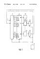
- FIG. 1shows a device with embedded multiport memory
- FIG. 2shows a timing diagram of a multiport memory
- FIG. 3shows a generic multiport memory module
- FIG. 4shows a MUX shell
- FIG. 5shows waveforms of signals in a MUX shell
- FIG. 6shows a clock generation circuit
- FIG. 7shows a state diagram of a finite state machine
- FIG. 8shows a restart delay circuit
- FIG. 9shows a RY circuit
- FIG. 10shows a dummy ready circuit
- FIG. 11shows a reset circuit
- FIG. 1shows a device with an embedded multi-port memory 10 .
- the devicecontains logic circuits 17 , coupled via a number of ports 12 a-c to the multiport memory 10 . Output ports of the memory are coupled to combinatorial logic circuits 14 a-b . Outputs of combinatorial logic circuits 14 a-b are coupled to registers 16 a-b , which in turn have outputs coupled to the logic circuit 17 .
- the devicecomprises a clock circuit 18 coupled to the logic circuits 17 , the multi-port memory 10 and the registers 16 a-b.
- the deviceoperates under synchronization by a clock signal from clock circuit 18 and it pipelines information.
- the logic circuits 17produce address signals A, data input signals D, port selection signals PS and write enable/read signals WE for the multi-port memory 10 .
- the port select signal PS for a certain portis active in a clock cycle, the multi-port memory 10 reads or writes data dependent on the WE signal at an address determined by the address signal A for that port.
- data from the multi-port memorybecomes available before the end of the clock cycle in which this data is made available from the memory.
- the time until the end of the clock cycleis used to subject the data to combinatorial logic operations, before storing a result in the registers 16 a -b at the end of the clock cycle.
- the datais passed from the registers 16 a-b to the logic circuits 17 for further processing.
- the logic circuits 17may contain further registers that are clocked by the clock signal.
- a port with read capabilityhas a data output Q.
- a port with write capabilityhas a data input D.
- a R/W porthas a write-enable input WE to select between reading and writing.
- Each port of a PMP memoryis comparable to the port of a standard single-port memory with a synchronous interface. All inputs are clocked at the rising edge of the clock input CLK. Then, sequentially, all ports are served starting with port 0 .
- FIG. 2shows a timing diagram of a read access via port 1 .
- Read/write conflictswhich may happen with a real multiport memory when two ports simultaneously access the same address location (one writing and the other reading or writing), will never happen because the ports are served sequentially.
- all portswill be of the R/W type for the purpose of illustration.
- the read-only and write-only type of portsare just derivatives of a R/W port.
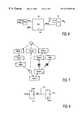
- FIG. 3shows a block diagram of the generic PMP architecture. It consists of a multiplexer shell 30 , an asynchronous controller 32 and a RAM or ROM instance 34 .
- FIG. 4shows a block diagram of the multiplexer shell.
- the multiplexer shellis configuration dependent. It implements the multiport function in standard-cells.
- the input signals (A, D, PS, WE) of each but the first portare stored in a register 40 at the rising edge of the clock input CLK.
- the input signals of the first portare not registered. These signals can propagate directly to the memory module.
- the multiplexer 42that follows the registers makes a selection out of the A, D, PS, WE (registered) inputs that correspond to one of the ports. The selection is controlled by a counter 43 which holds the active port. All flip-flops in the MUX shell and the memory module are triggered by the local clock signal clkInt.
- FIG. 5shows the signal waves inside the mux shell for a three port PMP.
- the clock period of the internal clock clkIntequals the access time (cycle time) of the memory. This is realized by using the ready output of the memory. It works as follows: (1) a memory access is started by a rising edge of clkInt, (2) the memory gives notices of its busy state by lowering RYmem, (3) the asynchronous controller replies by making clkInt low, (4) after some time, the memory access completion is signaled by a high level of RYmem. This last event restarts the sequence until all ports have been served.
- a read accessdiffers from a write access in that the data read from the memory must be copied to the Q register/latches corresponding to the active port.
- the shortest read access timescan be achieved when the data is stored in latches 44 .
- the strobe signal of the active portis 0-1-0 pulse having a width equal to the read-access time (see FIG. 5 ). During the strobe the latches [ 44 ] are transparent, otherwise the latest value is kept.
- the strobe busis deduced from clkInt, actPort, Rymem and “read” as follows:
- the shift register 45which drives the actPort bus holds the active port: the bit corresponding to the active port is high, the other bits are low.
- the signal readindicates that a read access is in progress.
- the signal “read”is generated with a D flip-flop 46 , which copies the logic “AND” of CS and (NOT WE) from the active port on the active edge of clkInt.
- the signals actPort and readare valid when clkInt is low.
- the rising edge of RYmemindicates that the data out of the memory is valid; consequently the strobe may become low after this event.
- the asynchronous controlleris configuration independent. It consists of a number of auxiliary circuits and an asynchronous finite state machine (FSM).
- FSMasynchronous finite state machine
- the asynchronous controllergenerates a rising edge on the internal clock for each port service. If the active port requires a memory access, which is being controlled by the corresponding PS input, the rising edge on the internal clock results in a handshake with the memory via the clkInt, RYmem signal pair (clkInt triggers the memory and RYmem indicates the completion of a memory access). If the active port is not selected, a handshake is performed with an auxiliary circuit which produces a dummy ready signals called RYdum.
- the controlleris triggered by the external clock CLK and continues to generate rising edges on the internal clock until the MUX shell signals, via preLast, that the last port has been completed.
- FIG. 6shows the synthesis of the internal clock clkInt.
- the AND-OR 60 gatemerges the external clock with the clock from the FSM 62 .
- the FSM 62has a well defined behaviour that can be formally described by a signal transition graph (STG).
- STGis an event-based specification for an asynchronous circuit. It is composed of transitions and places.
- a transitionrepresents a change of values of an input or output signal.
- a placerepresents a pre- and post-condition of transitions. It can be marked with a token, meaning that the corresponding condition holds in the circuit. When all pre-conditions of a transition are marked, the transition may fire which means that the tokens are removed from its pre-conditions and added to its post-conditions.
- a STGspecifies not only the behaviour of an asynchronous circuit but also of the environment in which it operates.
- the causality relations, described by places joining pairs of transitions,represent how the circuit and its environment can react to signal transitions.
- placesare shown as circles, transitions are shown as boxes and places with exactly one predecessor and one successor (implicit places) are omitted.
- the label of a transitionis composed of the signal name preceded by a “+” or a “ ⁇ ” indicating a rising and falling edge respectively.
- the STG of the FSM 62is given in FIG. 7 .
- Signal RYportindicates completion of either a memory handshake or a dummy handshake.
- Signal restartis the same as the start signal, however a little delayed (it changes when clkInt becomes low).
- FIG. 8shows the circuit for generating restart.
- Signal RYindicates the global ready state of the PMP module.
- the waveform of RYis given for a three port. This ready signal is used to merge the external clock with the clock from the FSM.
- FIG. 9gives the ready circuit.
- the circuitis designed such that the logical AND 90 of RY and CLK yields the first internal clock pulse.
- the ready stateis the logical AND 90 of RYport and start.
- the ready stateis combined with the CLK via a Muller-C element 92 .
- a Muller-C elementchanges to ‘1’ when both inputs are high and to ‘0’ when both inputs are low.
- a simple AND gatewould not do the job because this may potentially result in clock pulse that is too small when clkInt is heavily loaded.
- FIG. 10shows the circuit which produces the RYdum signal.
- itis a flip-flop that samples the CS input of the memory at the rising edge of the internal clock. If a zero is sampled, which means that the port does not result in a memory access, RYdum must generate a 1-0-1 pulse, just like RYmem, as explained in section. This is obtain by activating the asynchronous set input of the FF, when the internal clock becomes low.
- the reset circuit given in FIG. 11has been designed. It generates a reset pulse if the state of the PMP at the rising external clock edge is not equal to the final/initial state. This circuit will also become active if the controller has been trapped in a deadlock state due to EMC.
- the combinatorial delays in the shell 30should be shorter than the minimum delay from CLKInt via RYport.
Landscapes
- Engineering & Computer Science (AREA)
- Microelectronics & Electronic Packaging (AREA)
- Static Random-Access Memory (AREA)
Abstract
Description
Claims (8)
Applications Claiming Priority (2)
| Application Number | Priority Date | Filing Date | Title |
|---|---|---|---|
| EP98203219 | 1998-09-25 | ||
| EP98203219 | 1998-09-25 |
Publications (1)
| Publication Number | Publication Date |
|---|---|
| US6742088B1true US6742088B1 (en) | 2004-05-25 |
Family
ID=8234152
Family Applications (1)
| Application Number | Title | Priority Date | Filing Date |
|---|---|---|---|
| US09/400,958Expired - LifetimeUS6742088B1 (en) | 1998-09-25 | 1999-09-22 | Device containing a multi-port memory |
Country Status (5)
| Country | Link |
|---|---|
| US (1) | US6742088B1 (en) |
| EP (1) | EP1046172B1 (en) |
| JP (1) | JP2002526848A (en) |
| DE (1) | DE69910172T2 (en) |
| WO (1) | WO2000019438A1 (en) |
Cited By (5)
| Publication number | Priority date | Publication date | Assignee | Title |
|---|---|---|---|---|
| US20050216777A1 (en)* | 2002-10-03 | 2005-09-29 | Hitachi, Ltd. | Disk array device and method of supplying power to disk array device |
| US20090196109A1 (en)* | 2008-02-06 | 2009-08-06 | Micron Technology, Inc. | Rank select using a global select pin |
| US9490006B2 (en)* | 2014-12-08 | 2016-11-08 | Taiwan Semiconductor Manufacturing Company Ltd. | Time division multiplexed multiport memory |
| WO2018098307A1 (en)* | 2016-11-25 | 2018-05-31 | Hughes Network Systems, Llc | Novel ldpc decoder design to significantly increase throughput in asic by utilizing pseudo two port memory |
| CN118538263A (en)* | 2024-07-25 | 2024-08-23 | 中科亿海微电子科技(苏州)有限公司 | Time sequence control method and circuit for FPGA BRAM read-write conflict |
Families Citing this family (2)
| Publication number | Priority date | Publication date | Assignee | Title |
|---|---|---|---|---|
| JP5038657B2 (en)* | 2006-06-26 | 2012-10-03 | ルネサスエレクトロニクス株式会社 | Semiconductor integrated circuit device |
| US9287370B2 (en)* | 2012-03-02 | 2016-03-15 | Semiconductor Energy Laboratory Co., Ltd. | Memory device comprising a transistor including an oxide semiconductor and semiconductor device including the same |
Citations (7)
| Publication number | Priority date | Publication date | Assignee | Title |
|---|---|---|---|---|
| US4967398A (en)* | 1989-08-09 | 1990-10-30 | Ford Motor Company | Read/write random access memory with data prefetch |
| EP0471932A2 (en) | 1990-07-27 | 1992-02-26 | International Business Machines Corporation | Virtual multi-port ram |
| US5204841A (en)* | 1990-07-27 | 1993-04-20 | International Business Machines Corporation | Virtual multi-port RAM |
| US5301340A (en)* | 1990-10-31 | 1994-04-05 | International Business Machines Corporation | IC chips including ALUs and identical register files whereby a number of ALUs directly and concurrently write results to every register file per cycle |
| US5341473A (en)* | 1990-08-09 | 1994-08-23 | Nec Corporation | System of transferring data in a multi-CPU arrangement using address generators |
| US5612923A (en)* | 1996-05-09 | 1997-03-18 | Northern Telecom Limited | Multi-port random access memory |
| US6314499B1 (en)* | 1997-11-14 | 2001-11-06 | Lucent Technologies Inc. | Non-preemptive memory locking mechanism in a shared resource system |
Family Cites Families (3)
| Publication number | Priority date | Publication date | Assignee | Title |
|---|---|---|---|---|
| JPH01315857A (en)* | 1988-06-16 | 1989-12-20 | Oki Electric Ind Co Ltd | Shared memory access system |
| JP3107595B2 (en)* | 1991-06-18 | 2000-11-13 | 富士電機株式会社 | Memory access control device and memory access control method |
| IL109921A (en)* | 1993-06-24 | 1997-09-30 | Quickturn Design Systems | Method and apparatus for configuring memory circuits |
- 1999
- 1999-09-03WOPCT/EP1999/006550patent/WO2000019438A1/enactiveIP Right Grant
- 1999-09-03EPEP99946133Apatent/EP1046172B1/ennot_activeExpired - Lifetime
- 1999-09-03JPJP2000572853Apatent/JP2002526848A/enactivePending
- 1999-09-03DEDE69910172Tpatent/DE69910172T2/ennot_activeExpired - Lifetime
- 1999-09-22USUS09/400,958patent/US6742088B1/ennot_activeExpired - Lifetime
Patent Citations (7)
| Publication number | Priority date | Publication date | Assignee | Title |
|---|---|---|---|---|
| US4967398A (en)* | 1989-08-09 | 1990-10-30 | Ford Motor Company | Read/write random access memory with data prefetch |
| EP0471932A2 (en) | 1990-07-27 | 1992-02-26 | International Business Machines Corporation | Virtual multi-port ram |
| US5204841A (en)* | 1990-07-27 | 1993-04-20 | International Business Machines Corporation | Virtual multi-port RAM |
| US5341473A (en)* | 1990-08-09 | 1994-08-23 | Nec Corporation | System of transferring data in a multi-CPU arrangement using address generators |
| US5301340A (en)* | 1990-10-31 | 1994-04-05 | International Business Machines Corporation | IC chips including ALUs and identical register files whereby a number of ALUs directly and concurrently write results to every register file per cycle |
| US5612923A (en)* | 1996-05-09 | 1997-03-18 | Northern Telecom Limited | Multi-port random access memory |
| US6314499B1 (en)* | 1997-11-14 | 2001-11-06 | Lucent Technologies Inc. | Non-preemptive memory locking mechanism in a shared resource system |
Non-Patent Citations (4)
| Title |
|---|
| Endo et al. "Pipelined, Time-Sharing Access Technique for a Highly Integrated Multi-Port Memory", Apr. 1991 IEEE Journal of Solid-State Circuits v26 n4.** |
| Ken-Ichi et al: "Pipeliled, Time-Sharing Access Technique for an Integrated Multiport System", IEEE Journal of Solid-State Circuits, vol. 26, No. 4, pp. 549-554. |
| Matsumura et al. "Pipelined, Time-Sharing Access Technique for a Highly Integrated Multi-Port Memory", 1990 Symposium on VLSI Circuits IEEE.** |
| T. Sazaki, T. Komiya et al, "Time Division Pseudo-Multi-Port Register File With Wave Pipelining", Journal of the Soc. Of Elect. Information & Comm. D-, vol. J80-D-I, No. 3, pp. 223-226, Mar. 1997, and Transactions of the Institute of Electronics Information and Communication Engineers, vol. J80, No. 3 (1997) pp. 223-226. |
Cited By (8)
| Publication number | Priority date | Publication date | Assignee | Title |
|---|---|---|---|---|
| US20050216777A1 (en)* | 2002-10-03 | 2005-09-29 | Hitachi, Ltd. | Disk array device and method of supplying power to disk array device |
| US20090196109A1 (en)* | 2008-02-06 | 2009-08-06 | Micron Technology, Inc. | Rank select using a global select pin |
| US7948786B2 (en)* | 2008-02-06 | 2011-05-24 | Micron Technology, Inc. | Rank select using a global select pin |
| US20110216570A1 (en)* | 2008-02-06 | 2011-09-08 | Micron Technology, Inc. | Rank select using a global select pin |
| US8111534B2 (en)* | 2008-02-06 | 2012-02-07 | Micron Technology, Inc. | Rank select using a global select pin |
| US9490006B2 (en)* | 2014-12-08 | 2016-11-08 | Taiwan Semiconductor Manufacturing Company Ltd. | Time division multiplexed multiport memory |
| WO2018098307A1 (en)* | 2016-11-25 | 2018-05-31 | Hughes Network Systems, Llc | Novel ldpc decoder design to significantly increase throughput in asic by utilizing pseudo two port memory |
| CN118538263A (en)* | 2024-07-25 | 2024-08-23 | 中科亿海微电子科技(苏州)有限公司 | Time sequence control method and circuit for FPGA BRAM read-write conflict |
Also Published As
| Publication number | Publication date |
|---|---|
| EP1046172B1 (en) | 2003-08-06 |
| WO2000019438A1 (en) | 2000-04-06 |
| EP1046172A1 (en) | 2000-10-25 |
| DE69910172T2 (en) | 2004-05-19 |
| DE69910172D1 (en) | 2003-09-11 |
| JP2002526848A (en) | 2002-08-20 |
Similar Documents
| Publication | Publication Date | Title |
|---|---|---|
| US5793688A (en) | Method for multiple latency synchronous dynamic random access memory | |
| US4685088A (en) | High performance memory system utilizing pipelining techniques | |
| US4712190A (en) | Self-timed random access memory chip | |
| KR100945968B1 (en) | Semiconductor memory device | |
| US4887267A (en) | Logic integrated circuit capable of simplifying a test | |
| US5291580A (en) | High performance burst read data transfer operation | |
| JPS61148692A (en) | Memory device | |
| US6742088B1 (en) | Device containing a multi-port memory | |
| US5864252A (en) | Synchronous circuit with improved clock to data output access time | |
| US6327667B1 (en) | Apparatus and method for operating clock sensitive devices in multiple timing domains | |
| JPH04233646A (en) | Data transfer interface module | |
| JPH0556598B2 (en) | ||
| JP3305975B2 (en) | Address counter circuit and semiconductor memory device | |
| JP2697772B2 (en) | Information processing device | |
| KR20000025421A (en) | Access arbitration apparatus of common memory | |
| JP2003076602A (en) | Memory control method and memory control circuit | |
| JPH0827791B2 (en) | Microprocessor | |
| JPS59148191A (en) | Memory driving circuit | |
| JPH04149655A (en) | Memory card test system | |
| KR19990059133A (en) | How to read data from synchronous static RAM | |
| JPS6049333B2 (en) | Clock control method | |
| JPH08273353A (en) | Synchronous memory | |
| KR20010063503A (en) | Embedded processor having high performance memory architecture | |
| JP2000298980A (en) | Storing method and its device | |
| JPS6219945A (en) | Storage device |
Legal Events
| Date | Code | Title | Description |
|---|---|---|---|
| AS | Assignment | Owner name:U.S. PHILIPS CORPORATION, NEW YORK Free format text:ASSIGNMENT OF ASSIGNORS INTEREST;ASSIGNORS:WIELAGE, PAUL;VAN DER WERF, ALBERT;SEVAT, LEONARDUS H.M.;AND OTHERS;REEL/FRAME:010347/0630;SIGNING DATES FROM 19991007 TO 19991008 | |
| AS | Assignment | Owner name:KONINKLIJKE PHILIPS ELECTRONICS N.V., NETHERLANDS Free format text:ASSIGNMENT OF ASSIGNORS INTEREST;ASSIGNOR:UNITED STATES PHILIPS CORPORATION;REEL/FRAME:014513/0427 Effective date:20040412 | |
| STCF | Information on status: patent grant | Free format text:PATENTED CASE | |
| AS | Assignment | Owner name:NXP B.V., NETHERLANDS Free format text:ASSIGNMENT OF ASSIGNORS INTEREST;ASSIGNOR:KONINKLIJKE PHILIPS ELECTRONICS N.V.;REEL/FRAME:018635/0787 Effective date:20061117 | |
| FPAY | Fee payment | Year of fee payment:4 | |
| AS | Assignment | Owner name:UNISYS CORPORATION, PENNSYLVANIA Free format text:RELEASE BY SECURED PARTY;ASSIGNOR:CITIBANK, N.A.;REEL/FRAME:023263/0631 Effective date:20090601 Owner name:UNISYS HOLDING CORPORATION, DELAWARE Free format text:RELEASE BY SECURED PARTY;ASSIGNOR:CITIBANK, N.A.;REEL/FRAME:023263/0631 Effective date:20090601 Owner name:UNISYS CORPORATION,PENNSYLVANIA Free format text:RELEASE BY SECURED PARTY;ASSIGNOR:CITIBANK, N.A.;REEL/FRAME:023263/0631 Effective date:20090601 Owner name:UNISYS HOLDING CORPORATION,DELAWARE Free format text:RELEASE BY SECURED PARTY;ASSIGNOR:CITIBANK, N.A.;REEL/FRAME:023263/0631 Effective date:20090601 | |
| AS | Assignment | Owner name:NXP B.V., NETHERLANDS Free format text:CHANGE OF NAME;ASSIGNOR:PHILIPS SEMICONDUCTORS INTERNATIONAL B.V.;REEL/FRAME:026805/0426 Effective date:20060929 | |
| FPAY | Fee payment | Year of fee payment:8 | |
| AS | Assignment | Owner name:CALLAHAN CELLULAR L.L.C., DELAWARE Free format text:ASSIGNMENT OF ASSIGNORS INTEREST;ASSIGNOR:NXP B.V.;REEL/FRAME:027265/0798 Effective date:20110926 | |
| FEPP | Fee payment procedure | Free format text:PAYOR NUMBER ASSIGNED (ORIGINAL EVENT CODE: ASPN); ENTITY STATUS OF PATENT OWNER: LARGE ENTITY Free format text:PAYER NUMBER DE-ASSIGNED (ORIGINAL EVENT CODE: RMPN); ENTITY STATUS OF PATENT OWNER: LARGE ENTITY | |
| AS | Assignment | Owner name:KONINKLIJKE PHILIPS ELECTRONICS N.V., NETHERLANDS Free format text:CORRECTIVE ASSIGNMENT TO CORRECT THE EXECUTION DATE PREVIOUSLY RECORDED ON REEL 014513 FRAME 0427. ASSIGNOR(S) HEREBY CONFIRMS THE EXECUTION DATE IS 01/19/2004, NOT 04/12/2004;ASSIGNOR:UNITED STATES PHILIPS CORPORATION;REEL/FRAME:028309/0680 Effective date:20040119 | |
| FPAY | Fee payment | Year of fee payment:12 |