US6742068B2 - Data server with hot replaceable processing unit modules - Google Patents
Data server with hot replaceable processing unit modulesDownload PDFInfo
- Publication number
- US6742068B2 US6742068B2US08/884,740US88474097AUS6742068B2US 6742068 B2US6742068 B2US 6742068B2US 88474097 AUS88474097 AUS 88474097AUS 6742068 B2US6742068 B2US 6742068B2
- Authority
- US
- United States
- Prior art keywords
- processing unit
- motherboard
- printed circuit
- backplane
- circuit board
- Prior art date
- Legal status (The legal status is an assumption and is not a legal conclusion. Google has not performed a legal analysis and makes no representation as to the accuracy of the status listed.)
- Expired - Lifetime
Links
Images


Classifications
- G—PHYSICS
- G06—COMPUTING OR CALCULATING; COUNTING
- G06F—ELECTRIC DIGITAL DATA PROCESSING
- G06F9/00—Arrangements for program control, e.g. control units
- G06F9/06—Arrangements for program control, e.g. control units using stored programs, i.e. using an internal store of processing equipment to receive or retain programs
- G06F9/44—Arrangements for executing specific programs
- G06F9/4401—Bootstrapping
- G06F9/4406—Loading of operating system
- G—PHYSICS
- G06—COMPUTING OR CALCULATING; COUNTING
- G06F—ELECTRIC DIGITAL DATA PROCESSING
- G06F13/00—Interconnection of, or transfer of information or other signals between, memories, input/output devices or central processing units
- G06F13/38—Information transfer, e.g. on bus
- G06F13/40—Bus structure
- G06F13/4063—Device-to-bus coupling
- G06F13/4068—Electrical coupling
- G06F13/4081—Live connection to bus, e.g. hot-plugging
Definitions
- This inventionrelates generally to data servers and more particularly to data servers adapted to move data between a network and a data storage system.
- data serversare used to move data between a storage system, such as between a Symmetrix Integrated Cached Disk Array storage system and a network.
- the data servertypically includes a set AC powered processing unit modules each of which includes a central processing unit (CPU), input/output (I/O) adapter cards, and a main memory programmed to run a variety of software application programs for subscribers to the network. These applications include file access, video access and/or network backup.
- a set of five, AC powered, personal computers (PCs)are packaged inside a standard 19 inch cabinet. The five PCs are connected together via a twisted pair cable to an Ethernet hub. A laptop PC is used as a control station for the other PCs.
- a keyboard/monitor multiplexer (mux)was used to pass each PC's boot sequence with a single keyboard and monitor.
- a data serverhaving a plurality of hot replaceable processing unit modules.
- Each one of the processing unit modulesincludes a CPU, main memory and I/O adapter card.
- the data serverincludes a backplane having a first electrical connector adapted for coupling to a DC power supply.
- Each one of the processing unit modulesis DC powered.
- the moduleincludes a motherboard having plugged therein: the CPU; the main memory; and the I/O adapter card.
- the moduleincludes an interconnect printed board, electrically connected to the motherboard.
- the interconnect printed circuit boardhas mounted to it a second electrical connector and a DC to DC converter electrically connected to the second electrical connector.
- the second electrical connectoris adapted to mate with the first electrical connector to enable the processing unit module to be hot plugged into, or removed from, the backplane.
- a data serverhaving a cabinet with a plurality of slots, or compartments therein. Each one of the slots has a backplane disposed at the rear thereof.
- a plurality of hot replaceable, DC powered processing unit modulesis provided. Each one of the modules is adapted to be inserted in, or removed from, a corresponding one of the slots as such one of the processing unit modules is plugged into, or un-plugged from the backplane.
- a printed circuit boardis provided with a pair of overlying strip conductors forming a strip transmission line.
- the strip transmission lineis configured with electrical characteristics of a coaxial transmission line.
- the AC impedance and DC resistance of the strip transmission lineare selected to configure the strip transmission line as an Ethernet coaxial transmission line.
- a printed circuit backplanehaving an electrical connector adapted to mate with, and electrically connect to, an electrical connector of a daughterboard.
- the backplanehas a pair of overlying strip conductors forming a strip transmission line.
- the strip transmission lineis configured with electrical characteristics of a coaxial transmission line.
- the AC impedance and DC resistance of the strip transmission lineare selected to configure the strip transmission line as an Ethernet coaxial transmission line.
- a backplanehaving a first electrical connector mounted thereto adapted to have plugged therein a daughterboard.
- the daughterboardhas a second electrical connector adapted to mate with, and electrically connect to, the first electrical connector.
- the backplanehas a first strip conductor disposed on one a surface of a dielectric substrate thereof and a second strip conductor on an opposite surface of the dielectric substrate. The first and second strip conductors are in overlaying relationship to provide a strip transmission line from a coaxial connector mounted to the backplane to the first electrical connector.
- the strip transmission lineprovides an Ethernet bus on the backplane.
- a cable management systemfor a cabinet adapted to house electrical components.
- the cable management systemincludes at least one longitudinally extending channel disposed in the cabinet.
- a fasteneris provided adapted to open and enable the a cable to be inserted into the channel and close to retain such cable within the channel.
- the channelincludes a portion of a frame of the cabinet.
- a chassishaving a plurality of shelves for supporting electrical modules.
- a partitioning memberis provided having captive, manually operable hardware adapted for removable insertion onto one of the shelves.
- the shelfhas a pair of slots adapted to receive a pair of modules when the partitioning member is fastened to the shelf.
- Such shelfhas a single slot adapted to receive one module with width greater than the width of one of the pair of modules when the partitioning member is removed from the shelf.
- the partitioning members of one of the shelvesmay be removed from, or inserted onto, the shelf without interrupting operation of the modules on the other shelves.
- a power management systemincludes a cabinet having stored therein: a battery; a plurality of redundant, independently replaceable battery chargers. One of the pair of battery chargers may be replaced if defective without effecting the operation of the other one of the battery chargers in charging the battery.
- an I/O adapter card mounting platefor securing an array of I/O adapter cards to a case.
- Each one of the I/O adapter cardshas mounted thereto a mounting bracket.
- a motherboardis disposed in the case and is adapted to have plugged therein the array of I/O adapter cards.
- the mounting platehas captive fastening hardware and is adapted to be placed over the mounting bracket as a single piece.
- the captive hardwareis adapted to enable manual fastening of the mounting member to secure the mounting bracket between the mounting plate and the case after the array of I/O adapter cards has been plugged into the motherboard.
- an adapter card filler plateis provided.
- the filler platehas a plurality of holes formed therethrough to provide a honey-combed structure. If an I/O adapter card is not needed, an adapted card filler plate is substituted for it.
- the filler plateis fastened to a mounting bracket by the mounting plate.
- the honey-combed, adapted card filler plateimproves air-flow through the case.
- a methodfor booting operating system software into a main memory of a processing unit module.
- the methodincludes the step of executing a program stored in the processing unit module to sequentially search a plurality of possible sources of the operating system software during a boot-up phase.
- the CPUchecks to determine whether such detected source is operational and has a valid boot format. If the detected source is operational and has a valid boot format, the CPU boots the detected operating system software source into the main memory. If the detected source is either non-operational or does not have a valid boot format, the CPU checks another one of the possible operating system software sources. If all sources are checked and none are operational nor have a valid boot format, the CPU repeats the aforementioned sequential search of the possible operating system software sources.
- the processing unit moduleis able to successfully boot-up when the operating system software is stored in a relatively large memory system which may take a substantially long time to be operational compared to the relatively short boot-up time of the processing unit.
- FIG. 1is a diagram of a data server according to the invention coupled between a memory system and a network;
- FIG. 2is a drawing of the data server of FIG. 1;
- FIGS. 3A-3Care simplified, diagrammatical sketches of the data server of FIG. 1, FIG. 3A showing the front door of a cabinet used to store the components of the data server of FIG. 2, FIG. 3B showing the front of the cabinet when the front door of FIG. 3A is open; and FIG. 3C is a rear view of the cabinet when a rear door thereof is open.
- FIGS. 4A and 4Bare perspective views of the data server of FIG. 2;
- FIG. 4Abeing a rear perspective view of the data server with the rear door open;
- FIG. 4Bbeing a front perspective view of the data server with the front door open;
- FIGS. 4C and 4Dare front perspective and top diagrammatic drawings of the data server of FIG. 2 with the cabinet thereof being shown in phantom;
- FIG. 4Eis a rear view of a set of four backplanes used by the server of FIG. 2;
- FIGS. 5A-5Hare drawings of a processing unit module used as either a data mover or control station in the data server of FIG. 2; an exemplary one of the data movers and control stations being shown in FIGS. 5A-5G; FIGS. 5A, 5 B, 5 G showing an exemplary one of the data mover module; and FIGS. 5F and 5H show an exemplary one of the control station modules; FIGS. 5C and 5E are diagrammatical in nature and represent either a data mover or control station modules; FIG. 5D shows a processing unit module case prior to being configured as either a data mover or control station processing unit module;
- FIG. 6is a block diagram of a power management system, according to the invention, used in the server of FIG. 2;
- FIG. 7is a diagrammatical sketch showing a Ethernet strip transmission line, according to the invention, formed on a backplane and used to interconnect modules plugged into the backplane and coaxial cables used to interconnect a plurality of such backplanes;
- FIG. 8is a block diagram of the data server system of FIG. 1;
- FIGS. 9A though 9 Care drawings used to illustrate an I/O adapter card mounting plate according to the invention
- FIG. 9Ais a sketch of an array of such I/O adapter cards
- FIG. 9Bis an exploded cross-sectional diagrammatical sketch showing the arrangement between the mounting plate, an I/O adapted card and a mounting member provided on a front bezel of a module
- FIG. 9Cis an isometric, exploded drawing of the I/O adapter plate mounting member according to the invention
- FIGS. 9E-9Gare drawings of an I/O adapter card filler plate according to the invention adapted for use in place of an I/O adapter card in FIGS. 9A-9C, FIG. 9E being a perspective view of the filler plate and FIGS. 9F and 9G showing the filler plate of FIG. 9E mounted to the front bezel of a module;
- FIGS. 10A-10Fare drawing useful in understanding a the operation of a locking mechanism used by the modules; FIGS. 10A-10D showing the locking mechanism in the locked position and FIGS. 10E and 10F showing the locking mechanism in the unlocked position;
- FIGS. 11A-11Gare perspective views of a chassis used by the server of FIG. 2 to store up to four processing unit modules shown in FIG. 5A;
- FIG. 11Ashowing the chassis with partitioning members;
- FIGS. 11B and 11Cbeing perspective views of front and rear partitioning members, respectively, adapted for use with the chassis of FIG. 11A;
- FIG. 11Dbeing a perspective, exploded view of the chassis with the partitioning members of FIGS. 11B and 11C;
- FIG. 11Eis a sketch showing the chassis of FIG. 11A with the partitioning members of FIGS. 11A and 11B mounted therein to provide such chassis with four slots to receive four modules as shown in FIG. 11F;
- FIG. 11Gis a rear perspective view of the cabinet of FIG. 11A;
- FIGS. 12A-12Dare drawings useful in understanding “blind mating” between a module of FIG. 5 B and its mating backplane of FIG. 4C;
- FIGS. 13A and 13Bare drawings showing strip conductor circuitry disposed on a front and rear surface of a dielectric substrate used in the backplane of FIG. 4C, such strip conductors overlaying each other to form a strip transmission line Ethernet bus of FIG. 7;
- FIG. 14Ais a perspective view of the cabinet shown in FIG. 2, such view showing a cable management system according to the invention
- FIG. 14Bis an exploded view of a portion of the drawing in FIG. 11A such portion being inclosed by a circle labelled 14 B- 14 B in FIG. 14A
- FIG. 14Cis a top view of the cable management system
- FIG. 15is a diagram of the server of FIG. 2 connected to a test network during factory test.
- FIG. 16is a flow diagram of a method, according to the invention, for booting an operating system software into a main memory of each of the processing unit modules used in data movers and control stations of the data server of FIG. 2 during either factory test, as in FIG. 15 or during normal operation, as in FIG. 1 .
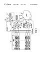
- a data server 10is shown coupled between a storage system 12 and a network 14 .
- the storage system 12is here a Symmetrix 3500 Integrated Cache Disk Array system manufactured and sold by EMC Corporation, Hopkington, Mass., assignee of the present patent application.
- the storage system 12is coupled to the data server 10 through a Fast Wide Differential (FWD) SCSI interconnect 16 , as shown.
- FWDFast Wide Differential
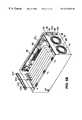
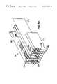
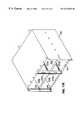
- the data server 10includes, in a single cabinet 18 shown in FIGS. 2, 3 A- 3 E, a plurality of, here up to sixteen hot replaceable processing unit modules 28 .
- Up to fourteen of the processing unit modules 28are data movers 20 , here labelled 20 1 - 20 14 and up to two of the processing unit modules 28 are control stations 22 here labelled 22 1 - 22 2 .
- the processing unit modules 28are all interconnected through a local bus, here an Ethernet bus 24 (FIG. 1 ).
- Hot replaceablemeans that a component can be removed and/or replaced without an interruption to the system's, here server's, operation.
- the modules 28are configured so that no cables need to be physically removed from the module 28 in order to remove it from the cabinet 18 .
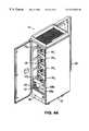
- FIG. 3BThere are sixteen slots, or compartments (FIG. 3B) in the cabinet 18 into which the processing unit modules 28 (i.e., data movers 20 1 - 20 14 or control stations 22 1 , 22 2 ) can be slidably inserted or removed.
- the slotsare arranged in longitudinally, here vertically, extending pairs; the top seven pairs being configured to receive data movers 20 1 - 20 14 , and the bottom pair being configured to receive the control stations 22 1 , 22 2 .
- One of the slots in the bottom paircan be configured as a fifteenth data mover 20 or it may be configured as a redundant control station 22 .
- the data movers and control stations 20 1 - 20 14 , 22 1 - 22 2are connected to the storage system 12 through the SCSI interconnect 16 , as noted above, and to the network 14 though bi-directional busses 26 , as shown in FIG. 1 .
- the control stations 22 1 , 22 2have different functions depending on the software application that is running on the data server 10 for a subscriber to the network 14 , for example.
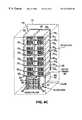
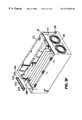
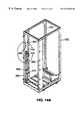
- Each data mover 20 1 - 20 14 or control station 22 1 , 22 2is disposed within a sheet metal case to provide an enclosure for the processing unit module 28 , as shown in FIGS. 4A and 4B.
- An exemplary one of the data movers and control station processing unit modules 28is shown in FIGS. 5A-5G. It is noted that FIGS. 5A, 5 B, 5 G show an exemplary one of the data mover 20 processing unit modules 28 , here data mover 20 , while FIGS. 5F and 5H show an exemplary one of the control station 22 processing unit modules 28 , here control station processing unit module 28 .
- FIGS. 5C and 5Eare diagrammatical in nature and represent either a data mover 20 or control station 22 .
- FIG. 5Dshows a processing unit module 28 , here an empty case, prior to being configured as either a data mover or control station.
- Each processing unit module 28is DC powered, environmentally controlled processing unit module.
- the processing unit module 28includes a motherboard having plugged therein a CPU, main memory, and I/O adapter cards, to be described in detail hereinafter. Suffice it to say here, however, is that the processing unit modules 28 are hot replaceable into, or from, the server 10 via four backplanes 30 1 - 30 4 (FIG. 3 C).
- processing unit modules 28 for data movers 20 1 - 20 4are hot replaceable via backplane 30 1 ; the processing unit modules 28 for data movers 20 5 - 20 8 are hot replaceable via backplane 30 2 ; the processing unit modules 28 for data movers 20 9 - 20 10 are hot replaceable via backplane 30 3 ; and, the processing unit modules 28 for data movers 20 11 - 20 14 and for control stations 22 1 , 22 2 are hot replaceable via backplane 30 4 .
- the data server 10also includes a CD ROM drive 50 , accessible when the front door 36 of cabinet 18 is opened, and a multiplexer board (MUX) 53 .
- a CD ROM drive 50accessible when the front door 36 of cabinet 18 is opened
- MUXmultiplexer board
- the data server 10includes a flat panel display 32 and keyboard with trackball mounted on the front door 36 of the cabinet 18 .
- the data server 10also includes a power management system 40 , to be described in more detail in connection with FIG. 6 . Suffice it to say, here, however that the data server 10 includes an Emergency Power Off (EPO) box 42 (i.e., a circuit breaker, line filters, controller and switches to enable switch over from primary AC main line 37 a power feed to auxiliary AC main line power feed 37 b ), a plurality of power supplies (e.g., AC to DC converters) 38 , one thereof being provided for redundancy.
- EPOEmergency Power Off
- the AC to DC converters 38are modular, redundant, and independently hot replaceable via a connector plate, not shown, mounted to an L-shaped printed circuit board 44 (FIGS. 3 C and 6 ).
- the battery back up unit (BBU) 46which includes battery 47 , is charged by a pair of redundant battery chargers 48 a, 48 b each independently hot replaceable via the connector plate, not shown, mounted to the L-shaped printed circuit board 44 , for charging the battery 47 .
- COMMBDspower control boards
- the COMMBDs 52will be described in more detail below in connection with FIG. 6 and the power management system 46 . Suffice it to say here, however, that the COMMBDs 54 are coupled to the server backplanes 30 1 - 30 4 though the L-shaped printed circuit board 44 , as shown in FIG. 6 .
- Each COMMBD 54is adapted to sense a variety of conditions, including: which data movers 20 1 - 20 14 are present in each data mover backplane 30 1 - 30 4 ; which backplanes 30 1 - 30 4 are present; whether there are Ethernet bus 50 ohm terminator resistors 56 , to be described in more detail in FIG.
- the L-shaped printed circuit board 44is the wiring backbone of the data server 10 . There are two facets to the L-shaped printed circuit board 44 : there are connections on the L-shaped printed circuit board itself to enable its connection to the backplanes 30 1 - 30 4 by a ribbon cables 31 ; and, there is a connector plate, not shown, mounted to the L-shaped printed circuit board 44 for plugging in the EPO box 42 and battery chargers 48 a, 48 b allowing for “quick-disconnect” of the batteries chargers 48 a, 48 b.
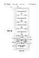
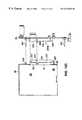
- FIG. 8a system block diagram of the data server 10 is shown.
- the processing unit modules 28i.e., data movers 20 1 - 20 14 and control stations 22 1 , 22 2
- communicate with each other through an Ethernet bus 24here a pair of redundant Ethernet busses 24 a, 24 b, as shown, to the network 14 via an ATM, Ethernet or FDDI bi-directional buses 26 (FIG. 1 ), for example, and to storage system 12 via the FWD SCSI, or Fibre channel interconnect 16 (FIG. 1 ).
- control stations 22 1 , 22 2each includes a floppy disk 60 and optional hard drive 62 .
- the control stations 22 1 , 22 2are also here shown connected to the network 14 with ATM buses, however, it should be understood that other buses may be used such as Ethernet or FDDI, for example.
- the control stations 22 1 , 22 2are connected to the storage system 12 through SCSI channels 16 , here a pair of redundant SCSI channels.
- the control stations 22 1 , 22 2are adapted for coupling to modems, not shown, via communication, or COMM ports 64 , as indicated.
- the control station 22 1 , 22 2motherboards 67 , to be described in connection with FIGS.
- 5C, 5 Eare provided with keyboard, mouse, VGA and IDE interface cards 66 for enabling connection to a flat panel display 32 , keyboard 34 , mouse and CDROM drive 50 via multiplexer 53 , as indicated.
- the control stations 22 1 , 22 2have access thereto though the multiplexer 74 . Therefore, the two control stations 22 1 , 22 2 share a common display 32 , keyboard 34 , mouse and CDROM 50 .
- One of these control stations 22 1 , 22 2can act as a redundant control station so that if one of the two control stations 22 1 , 22 2 fails, the other one is still operational.
- the pair of Ethernets 24 a, 24 b(FIG. 6) fails, the data server 10 can operate with the other one.
- FWD SCSI channels 16 a, 16 bIf one of the storage channels, here FWD SCSI channels 16 a, 16 b, fails, the other one still enables communication with the storage system 14 . As noted above, there is redundancy in AC-DC converters 38 and battery chargers 48 a, 48 b.
- the control stations 22 1 , 22 2are responsible for communications interconnect between themselves and the data movers 20 1 - 20 14 , via server interconnect printed circuit boards 68 in each control station 22 1 , 22 2 and data mover 20 1 - 20 14 .
- the system interfacese.g., environmental, internal Ethernet communications, modem, and network and storage
- the particular functions of the control stations 22 1 , 22 2may vary depending upon the application in use, but generally include: management of the individual data movers 20 1 - 20 14 , power management and cooling (i.e., environmental) management.
- the control stations 22 1 , 22 2include, in addition to the motherboard 67 (FIG. 5E) with six I/O adapter card slots, a 3.5 inch high density floppy disk drive 60 , as shown in FIG. 5 H.
- the processing unit modules 28are powered by AC-to-DC converters, i.e. power supplies) 38 which are fed by the dual line AC through the EPO box 42 to the AC-to-DC converters 38 .
- the output of the AC-to-DC convertersis here 48 volts DC and is fed to each of the DC to DC converters 70 mounted to each of the server interconnect printed circuit boards 68 (FIG. 5E) included within each one of the processing unit modules 28 , described above.
- BBUbattery backup unit
- AC powermay be lost up to several minutes, during which time the battery 47 in the BBU 46 will power the server 10 .
- Chargeis maintained in the BBU 46 by one of the two, independently hot replaceable battery chargers 48 a, 48 b. It was recognized that what typically fails in a system having a backup battery 47 (FIG. 6) is the battery charger. Thus, here, the battery chargers 48 a, 48 b are external to the battery 47 and each of the chargers 48 a, 48 b, one being redundant, is hot replaceable, as shown in FIGS. 4A, 4 B, 6 .
- the technicianmerely hot un-plugs the failed one of the two battery chargers 48 a, 48 b and replaces it with an operational battery charger while the server 10 continues to operate without interruption.
- the AC-DC converters 38provide power to the processing unit modules 28 via a 48 volt bus system (i.e., a+48 volt bus and a ground bus) and one of the battery chargers 48 a, 48 b supplies a trickle charge to the battery 47 .
- the output voltage of the AC/DC converters 48is slightly above 48 volts to back bias diode 72 a (FIG. 8) while diode 72 b (one diode being included in each converter 48 ) is forward biased.
- power to the processing unit modules 28is supplied by the battery 47 via the 48 volt bus to the backplanes 30 1 - 30 4 .
- the one of the two battery chargers 48 a, 48 b producing the highest potentialis selected as the one to charge the battery 47 .
- the data server 10has n plus one AC-to-DC converters 38 (i.e., power supplies 38 ); here, n is five.
- Each processing unit module 28includes an interconnect printed board 68 , electrically connected to (i.e., plugged into) the motherboard 67 .
- the interconnect printed circuit board 68i.e., a daughterboard for the backplane 30
- the electrical connector 93 of the interconnect printed circuit board 68is adapted to mate with, and electrically connects to, one of the backplane 30 1 - 30 4 electrical connectors 254 a, 254 b, 254 c, or 254 d (FIG. 12 B).
- DC power from the 48 volt bus systemis connected to pins of the backplane 30 1 - 30 4 connectors 254 a - 254 d.
- the DC to DC converter 70 electrically connected to the electrical connectors 254 a - 254 dthen distributes the 48 volts to other components of the processing unit module 28 and enables the processing unit module 28 to be hot plugged into, or removed from, the backplane 30 1 - 30 4 .
- each one of the processing unit modules 28includes a server interconnect printed circuit boards 68 .
- each one of the boards 68has mounted to it a DC-to-DC converter 70 .
- the DC to DC converter 70creates the required DC voltages (i.e., here +3.3, +5 volts, +12 volts, etc.) from a bulk 48 volt on the 48 volt bus that is distributed throughout the cabinet 18 . More particularly, the 48 volts is then converted by the DC to DC converter 70 mounted to the server interconnect printed circuit board 68 to the voltages required by components, i.e., fans, CPU, optional disk drive, etc. in the processing unit module 28 . These required voltages may be, for example, 5 volts DC, 12 or 3.3 volts DC.
- the server interconnect printed circuit boards 68each have mounted to them a pair of redundant Ethernet transceivers (XCVRs).
- each data mover 20 1 - 20 14 or control station 22 1 , 22 2is disposed within a sheet metal case to provide a processing unit module 28 , an exemplary one being shown in FIGS. 5A-5H.
- Each casehouses a DC powered, environmentally controlled processing unit module 28 .
- the processing unit module 28includes the motherboard 67 (FIG. 5E) disposed on the bottom of the processing unit module 28 , the data server interconnect printed circuit board 68 mounted along one side of the processing unit module 28 , and a pair of DC fans 76 , 78 disposed on the back of the processing unit module 28 .
- the server interconnect printed circuit board 68has mounted to it the DC to DC converter 70 (FIG. 8 ), a DC margin and thermal control unit module, a pair of control busses, a pair of Ethernet 10 Base2 busses, a parallel port interface and various indicators 77 and switches 79 (FIGS. 5G and 5H) accessible from the front panel of the processing unit module 28 .
- the thermal control unit processing unit module 28is used to control the fans 76 , 78 , and hence the environment, of such processing unit module 28 .
- the processing unit module 28 interconnect printed circuit board 68i.e., a daughterboard plugs into the motherboard 67 (FIG. 5 E).
- the DC fans 76 , 78have a tachometer, not shown. and the server interconnect printed board 68 has fan detection logic that determines if the fans 76 , 78 are still rotating properly. If a fan failure has occurred a fan_tach fault is presented to the control stations 22 via the backplane 30 1 - 30 4 .
- the control stations 22provide the mechanism in which to turn on/off the power to an individual data mover/control station processing unit module 28 . Airflow through the data mover/control station processing unit module 28 is from front to back, as shown in FIG. 4 B.
- the DC operated fans 76 , 78pull air from slots in the front panel (FIG. 5B) of the data mover/control station processing unit module 28 and across the motherboard 67 .
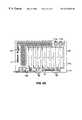
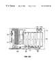
- the motherboard 67(FIG. 5E) has mounted to it a central processing unit (CPU) 80 , here a Pentium processor, a cache memory, main memory 82 a (FIG. 5C) (i.e., RAM SIMM modules adapted for insertion into conventional SIMM slots 82 ), PCI bus slots 84 , ISA bus slots 86 .
- the slots 84 , 86are adapted to receive plug-in standard I/O adapter cards, an exemplary array 85 being shown in FIG. 9 A. (As will be described, the data movers 20 1 - 20 14 here have four PCI slots 84 , 86 and four ISA slots (FIG.
- the I/O adapter cards 85may also include SCSI, ATM, Ethernet FDDI and ESCON cards, for example.
- the motherboardalso has mounted to it a flash memory, or ROM having stored therein the CPU 80 self-test program (and BIOS).
- the processing unit module 28is configured to enable use of market available processing unit module motherboards and I/O adapter cards 85 .
- Motherboardsmay range anywhere from five slot machines to eight slot machines, for example.
- the motherboard 67is an Intel PBP133ED70NC.
- the data mover or control station processing unit module 28has eight I/O adapter card slots 84 , 86 (i.e., 3 PCI, 4 ISA, and 1 mixed PCI/ISA). It also has 4 SIMM slots 82 (FIG. 5 E), uses a Triton Chipset, and is capable of 100 MB sustained throughput between processing unit 28 main memory 82 a and the PCI bus.
- the two leftmost slots 84house single channel SCSI cards, for example, that interface to the storage devices in the data storage system 12 (FIG. 1 ).
- the next two slots 84are for connection to the network 14 (FIG. 1) (i.e., combinations of 100base T Ethernet, FDDI, ATM or other adapters); the following two slots 86 to the right of the network connectors are here reserved for expansion, and the two rightmost slots 86 are 10baseT Ethernet bus for communications between the data mover and the control stations 22 1 , 22 2 .
- a fully loaded data server 10has 60 slots 84 , 86 that can be configured with network and/or storage I/O adapter cards 85 .
- Each server motherboard 67has four available full length PCI slots and each control station has two available full length PCI slots.
- An exemplary data server 10is configured with four-port Ethernet network adapters and single SCSI adapters would yield a system with one hundred and twenty network 12 connections and thirty data storage system 14 connections.
- the server interconnect printed board 68provides the status, control and communication interfaces for the server 10 .
- the server interconnect printed circuit boards 68serve as a bridge between the motherboard 67 and the server 10 via the backplanes 30 1 - 30 4 .
- the server interconnect printed board 68performs the following functions: (1) It provides a point of load DC-to-DC conversion for the motherboard 67 ; (2) It contains a control bus that allows the control station processing unit module 28 to perform numerous environmental operations to the data mover processing unit modules 28 ; (3) It collects the environmental status that is local to the data mover and/or control station processing unit module 28 and reports on exceptional conditions; (4) It contains an Enhanced Parallel Port (EPP) which allows the motherboard 67 to gather Vital Product Data (VPD) and other configuration information, enables their battery backup functions, solicits on exceptional system conditions, signals the control station via the control bus, and accesses other system interfaces; (5) It contains a Legacy Parallel Port (LGP) that interfaces the control station to the COMM board (COMMB
- a Teradyne High Density Metric (HDM) connector 93is mounted to the rear of server interconnect printed circuit board 68 .
- the rear of the HDM connector 93projects outward from a slot 94 provided in the rear panel 98 of the processing unit module 28 (FIGS. 5 D and 5 F); FIG. 5F showing processing unit module 28 with the interconnect printed circuit board 68 removed.
- the upper portion 95 of connector 93is adapted to receive the 48 volts provided by the AC/DC converters 38 (FIGS. 6 and 8) on the 48 volt bus system.
- the middle and lower portions 97 , 99 of the connector 93(FIG.
- FIG. 5Bare adapted to receive signals via the backplanes 30 1 - 30 4 .
- Disposed between the middle and lower portions 97 , 99 of connector 93is a hole 101 .
- the rear panel 98 of the processing unit module 28(FIG. 5B) is provided with a hole 105 , as shown, disposed below the connector 93 .
- this arrangementis used in a three-step “blind mating” arrangement enabling hot replacement of the processing unit module 28 from a backplane 30 1 - 30 4 into which the processing unit module 28 plugs.
- the front panel bezels 110 of the data mover 20 , module 28 and control station 22 , module 28are shown, respectively.
- the front bezels 110have a handle 111 , as shown.
- On the front bezels 110 of eachare several switches 79 and indicators 77 . More particularly, a service switch used only for manufacture, power enable LED indicators to indicate that power is enabled within the data mover 20 1 - 20 14 , or control station 22 1 - 22 2 ; a fault LED to indicate a failure in the control station or data mover module 28 , a push button reset switch to perform a hard reset to CPU 80 mounted on the motherboard, and status LEDs.
- the reset switchis a mechanical switch which restarts the CPU 80 to initiate a boot of the operating system software into the main memory 82 a.
- a programis stored in the processing unit module 28 (a portion in the flash memory mounted to the motherboard 67 , mentioned above, and another portion on the Ethernet adapter cards plugged into the motherboard 67 ) to automatically reset the CPU 80 until the CPU 80 finds an operational and valid source for the operating system software.)
- there are twelve small status LEDs 77(FIGS. 5G, 5 H) to provide additional information about the internal state of the data mover and/or control station module.
- the front bezel 110 of the control station 22 module 28shows the physical location of the I/O adapter card slots 84 , 86 .
- slot numbers 3 and 4are PCI slots and slots 5 through 8 are ISA slots.
- FIG. 5Gshows the front bezel 110 of the data mover and the physical location of the I/O adapter card slots 84 , 86 .
- slots 1 through 4are PCI slots.
- Slot numbers 5 through 8are ISA slots.
- the front bezel 110is provided with a pair of openings 113 a, 113 b (FIG. 7) to enable connection of the pair of redundant Ethernet I/O adapter cards via connectors 113 c, 113 d (FIG.
- the data movers/control stationscomprise of a motherboard 67 , a server interconnect printed circuit board 68 , I/O adapter cards 85 , DC powered fan 76 , 78 , and a mechanical enclosure, or case for the processing unit module 28 .
- the casehas a latching mechanism 222 to be described in connection with FIGS. 10A-10F.
- the modules 28include on their front bezels 110 panel, a handle 111 and locking mechanism 222 that is used, as described above, to insert or remove the module 28 from the cabinet 18 .
- the I/O adapter card slots 1 - 8 for data movers 20 1 - 20 14 and slots 3 - 8 for control stations 22 1 , 22 2are visible from the front bezels 110 of the data mover or control station module 28 .
- FIG. 9 AAn exemplary array of I/O adapter cards 85 is shown in FIG. 9 A. It is noted that the I/O cards 85 are off-the-shelf printed circuit boards having an L-shaped mounting bracket 301 . Each one of the L-shaped mounting brackets 301 has a leg portion 304 fastened to a printed circuit board, or card 302 and a foot portion 306 with a U-shaped opening 308 passing through the foot portion 306 normally used to receive a screw, not shown, used to securing the bracket 301 to a mounting member 310 of the case (i.e., module 28 enclosure), for example.
- the L-shaped mounting bracket 301is, noted above, affixed to a printed circuit card 302 .
- the printed circuit card 302is adapted to have its bottom edge 303 plug into one of the slot 84 , 86 (FIG. 5E) in the motherboard 67 .
- a mounting plate 312 having a plurality of captive screws 314is used.
- the mounting plate 312has press fit into a plurality of holes 316 (FIG. 9C) formed therein a corresponding plurality of screw fixtures 320 , here manufactured by Penn Engineering and Manufacturing Company, Danboro, Pa. 18916, and a plurality of press fit pins 317 having tips 317 a which project from the bottom of the plate 312 as a single unit to engage the U-shaped openings 308 in place of individual screws.
- the screw fixtures 320have an outer collar which is press-fit into the holes 316 in the mounting plate 312 to thereby secure the screw fixtures 320 to the mounting plate 312 as a single unit.
- the screws 314are rotatably mounted within the screw fixtures 320 .
- the bottom of the mounting plate 312is set over the horizontal foot portion 306 of the L-shaped mounting brackets 301 , as shown in FIG. 9 B.
- the technicianuses his/her thumb and forefinger about the outer periphery of the screws 314 , turns the screws 314 within the fixture 320 clockwise to screw the screws 314 into the corresponding, tapped and threaded holes 340 provided in the front panel 110 mounting member 310 thereby mounting the entire mounting plate 312 to the front panel 110 mounting member 310 .
- the mounting plate 312when secured to the front panel mounting member 310 , fastens the L-shaped brackets 304 to such front panel mounting member 310 .
- the technicianturns the screws 314 counter-clockwise until the mounting plate 312 is released from the front panel mounting member 310 . The technician then lifts and removes the mounting plate 312 .
- the technicianunplugs the desired I/O adapter card or cards 85 .
- the screwsare captive to the mounting plate 312 (i.e., the screws 314 in their fixtures 320 are captive hardware to the mounting plate 312 ).
- the mounting plate 312is a relatively large piece. Therefore, instead of having to contend with six or eight individual screws, which are relatively small, difficult to handle individually, and subject to being dropped and difficult to retrieve, the single, relatively large mounting plate with captive hardware greatly facilitates the insertion and/or removal of the I/O adapter cards 85 . Still further, a screw driver is not required.
- the filler plate 350has an L-shaped mounting bracket 301 ′ with a foot portion 306 .
- the foot portion 306has an U-shaped opening 308 similar to that for the I/O adapter card 302 mounting brackets 301 , described above.
- the leg portion 351has a plurality of holes 352 formed therethrough to provide a honey-combed structure. If one of the I/O adapter cards 302 is not needed, one of the adapted card filler plates 350 is substituted for it, as shown in FIGS.
- FIGS. 3C-3Ethe relationship between the server backplanes 30 1 - 30 4 and the data movers 20 1 - 20 14 processing unit modules 28 and control stations 22 1 - 22 2 processing unit modules 28 , is shown.
- four backplanes 30 1 - 30 4connect up to fourteen stream servers 20 1 - 20 14 and two control stations 22 1 - 22 2 .
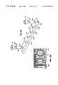
- fastened within in the cabinet 18is a set of four sheet metal chassis 200 , an exemplary one thereof being shown in FIG. 11 A.
- Disposed between upper and lower panels 202 , 204is an intermediate shelf 206 fastened to opposing side panels 210 .
- Partitioning members 212 a, 212 b(FIG.
- the chassis 200is adapted to receive four modules 28 , as described above, as shown in FIG. 11 F.
- the partitioning members 212 a, 212 bmay be removed allowing insertion of a larger module 28 case.
- the single module 28 casewould have its server interconnect printed circuit board connector 93 (FIG. 5B) on the left side of its case so that when the single module 28 case is slide onto the shelf the connector 93 will be able to be plugged into (i.e., mate with) the backplane 30 1 - 30 4 .
- a screw 253(FIG. 11G) is adapted to pass through holes 253 a in the backplane (FIGS. 12B, 13 A and 13 B) and be threaded into a hole 253 d in the rear wall 253 c of partitioning member 212 b.
- the back panel 240 of the chassis 200four slots 241 a, 241 b to enable the connectors 93 of each of the four modules 28 to project therefrom. If a single module 28 is used on any one of the two shelves 204 , 206 , the connector 93 of such module 28 will project from the appropriate one of the slots 241 a.
- the front of the side panels 210are provided with slots 218 , as shown in FIGS. 11A, 11 D. As will be described, such slots 218 are adapted to engage the locking mechanism 222 (FIGS. 5G and 5H) on the module 28 to lock/unlock the module 28 in the cabinet 18 .
- the chassis 220has a rear panel 240 fasten to it, here welded, as shown in FIG. 11 G.
- the rear panel 240is provided with nine posts 242 (FIG. 11E) to receive corresponding nine holes 248 passing though a corresponding one of the four backplanes 30 1 - 30 4 , an exemplary one being shown in FIG. 12A and 12B, the chassis 200 not being shown for clarity.
- the rear panel 240carries captive screws 243 which are adapted to pass through holes 253 a in the backplane (FIGS. 13A, 13 B) into a threaded rear wall 235 c (FIG. 11C) in partitioning member 212 b (FIG. 11 C).
- the backplanes 30 1 - 30 4are identical in construction, an exemplary one thereof, here backplane 30 1 being shown in FIGS. 12A and 12B.
- the backplane 30 1is a multi-level printed circuit board.
- the front of the backplane 30 1is shown in FIG. 12A to include four oval apertures 250 a - 250 d (FIG. 11A) adapted to align with the four oval openings 252 a - 252 d provided in the chassis 200 rear panel 240 (FIG. 11 E).
- Four Teradyne HDM connectors 254 a - 254 d(FIGS.
- Each Teradyne HDM connector 254 a - 254 dincludes a forward projecting alignment pin 260 , as shown for exemplary connector 254 a in FIGS. 12C and 12D.
- Each backplane 30 1 - 30 4has fastened to it four longer alignment pins 261 , as shown more clearly in FIGS. 12C and 12D.
- a Teradyne High Density Metric (HDM) connector 93is mounted to the rear server interconnect printed circuit board 68 (FIG. 12 D). More particularly, the server interconnect printed circuit board 68 is loosely mounted to the case 28 so that it may move slightly upward if needed in mating connector 93 with connector 254 a.
- the rear of the HDM connector 33projects outward from a slot 94 provided in the rear of the module 28 (FIG. 5F) and in the rear panel 242 of chassis 200 (FIG. 11 E); FIG. 5F showing module 28 with the interconnect printed circuit board 68 removed.
- the upper portion 95 of connector 93is adapted to receive the 48 volts provided by the AC/DC supplies 38 (FIG.
- the mid and lower portions 97 , 94 of the connector 93are adapted to receive signals. Disposed between the mid and lower portions 97 , 94 of connector 93 is a hole 41 , as described above in connection with FIG. 5 B.
- the rear panel 98 of the module 28(FIG. 5B) is provided with a hole 105 , as shown, disposed below the connector 93 .
- the HDM connectors 93 of the data movers 20 1 - 20 4plug into backplane 30 1 ; the HDM connectors 93 of data movers 20 5 - 20 8 plug into backplane 30 2 ; the HDM connectors 93 of data movers 20 9 - 20 12 plug into backplane 30 3 ; and the HDM connectors 93 of data movers 20 13 , 20 14 and of control stations 22 1 , 22 2 plug into backplanes 30 4 .
- the control stations 22 1 , 22 2 modules 28 as well as the data movers 20 1 - 20 14 modules 28are hot replaceable directly (i.e., without any cables between the module 28 and the backplane 30 1 - 30 4 and without any interruption to the operation and data processing of the server 10 ).
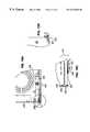
- the plugging of a module 28 into the backplane 30 1is a three-step process.
- the tip of shorter pin 260 of HDM connector 254 aengages the hole 101 in HDM connector 93 thereby guiding the connector 93 onto the shaft of the pin 260 .
- the server interconnect printed circuit board 68is loosely mounted to the module 28 so that it may move slightly in the module 28 as hole 101 and pin 260 engage each other.
- the plastic housings 257 , 259 of the HDM connectors 93 , 254 aengage each other. This procedure enables “blind-mating” between the module 28 (i.e., the sheet metal case of the module 28 ) and the backplane 30 , thereby enabling the module 28 to be hot plugged into, or removed from the backplane 30 1 , and hence into the data server 10 (FIG. 1 ).
- the module 28is plugged into DC provided by the power supplies 38 (FIG. 6 ), as distinguished from AC.
- the processing unit module 28has its own CPU 50 , I/O adapter cards 85 , main memory 82 a and the DC/DC converter 70 , is being hot plugged into, or removed from a here 48 volt DC source; i.e., a 48 volt battery backed DC supply 38 .
- each module 28is locked into the cabinet 18 . More particularly, as described above, the bottom of each module 28 has pivotally mounted to the front, lower left corner thereof a locking mechanism 222 , as shown more clearly in FIGS. 5 D and 10 A- 10 F.
- the locking mechanism 222is an arm 223 pivotally mounted at point 224 (FIG. 10C) to the bottom of the module 28 . It is noted that the left side 226 of the locking mechanism arm 223 projects beyond the side 228 of module 28 , as shown when the right side 229 of the arm 223 is manually urged rearward against the chassis 28 ; i.e., in the position shown in FIGS. 10A-10C.
- the technicianrotates the right side 229 of the arm 223 (i.e., the handle) forward, i.e., in the direction of arrow 231 (FIG. 10 C), so that the left side 226 of the arm 223 rotates rearward into a slot 230 provided in the left side 226 of the module 28 , as shown in FIGS. 10D-10F.
- the left side 226 of arm 223no longer projects beyond the left side 228 of the module 28 (FIG. 10 F), but rather swings rearward and becomes recessed in the slot 230 provided in the left side 226 of the module 28 .
- the module 28is slid onto the lower panel, or shelf, as the case may be, of the chassis 200 (FIG. 11 D).
- the technicianurges the right side 229 of the arm 223 forward causing the left side 226 of the arm 223 to pivot rearward (i.e., in the reverse direction of arrow 23 ) into the slot 218 (FIGS. 11C, 11 D) provided in the side 206 of the chassis thereby locking the module 220 in the chassis, i.e., preventing its removal unless the technician decides to remove the module 28 by again urging the right side 229 of the arm 223 forward, as described above.
- screw 225(FIG. 10A) in arm 223 screws into hole 225 a (FIG. 10 D).
- the backplanes 30 1 - 30 4are multi-layer printed circuit boards. Patterned into the front and back surfaces of one of the dielectric layers (referred to collectively herein as a dielectric substrate) of the printed circuit boards of the backplane 30 1 - 30 4 are strip conductor circuitry 262 F, 262 B, as shown in FIGS. 12A and 12B, respectively. Patterned into the front and back surfaces of another one of the printed circuit board layer of the backplane 30 1 - 30 4 are strip conductor circuitry, not shown for a redundant Ethernet bus. The two layers are bonded together with suitable dielectric insulation to prevent electrical short circuits developing between the redundant Ethernet busses 24 .
- the strip conductor circuitry 262 F, 282 Bmeanders, as shown, from a first Ethernet connector 270 a, serially to a pair of pins 274 , 276 of each of the Teradyne connectors 254 a - 254 d to a second Ethernet connector 270 b thereby providing the local Ethernet bus 24 a (FIG. 1) interconnecting the four modules 28 plugged into the backplane 30 1 .
- Ethernet connectors 270 ′ a, 270 ′ bare used for the redundant bus 24 b, not shown).
- Ethernet connectors 270 a, 270 b, 270 ′a - 270 ′ dare here BNC 10Base2 Ethernet connectors, mounted adjacent to a corresponding one of the apertures 250 a - 250 d.
- Each Ethernet connector 270 a - 270 bis a coaxial connector having a center conductor 280 (FIG. 12A) and an outer conductor 282 (FIG. 11 B).
- the center conductors 280 of the four Ethernet coaxial connectors 270 a, 270 bare connected to strip conductor circuitry 262 F while the outer conductor 282 is connected to strip conductor circuitry 262 R.
- the strip conductors 262 F, 262 Roverlay one another as they pass from the first Ethernet connector 270 a to the second Ethernet connector 270 b. Further, the width of the return strip conductor 262 R is wider that the width of the signal strip conductor 262 F thereby providing a strip transmission line.
- the AC impedance and DC resistance of the overlaying strip conductori.e., the strip transmission line
- the strip transmission lineare designed to have the substantially the same AC impedance and DC resistance of an Ethernet coaxial transmission line.
- the AC impedance and DC resistance of the overlaying strip conductoris designed to provide an AC impedance, Z, of 50 ohms and a DC resistance, R, of 1.37 milli-ohms per inch.
- Z87 ( e ⁇ + 1.41 ) 1 / 2 ⁇ ln ⁇ ⁇ 5.98 ⁇ ⁇ h ( .8 ⁇ ⁇ w + t )
- R⁇ ⁇ ⁇ ( L / A ) ⁇ ⁇ ⁇ ⁇ / inch
- wis the width of the signal strip conductor 262 F
- his the thickness of the dielectric layer
- tis the thickness of the signal conductor 262 F
- ⁇is the resistivity of the signal or return conductor 262 F, 262 R
- Lis the length of the signal conductor 262 F and
- Ais the area of the signal conductor 262 F
- the return conductor 262 Rserves as an radio frequency ground plane for the signal conductor 262 F and therefore should be wider that the signal conductor 262 F. That is, the signal on the Ethernet bus 24 a, 24 b has a frequency of 10 MHz.
- the overlaying signal conductor 262 F and return conductor 262 F(with the intermediate dielectric printed circuit board layer) provide a strip transmission line for the Ethernet 10 MHz signal.
- the return conductor 262 Reffectively serves an a non-DC ground, RF ground plane for the strip transmission line and is here 5 times greater in width than the width, w, of the signal conductor.
- the Ethernet busses 24 a, 24 b on the backplane 30 1are formed as strip transmission lines. That is, the backplane printed circuit board is provided with a pair of overlying strip conductors forming a strip transmission line.
- the strip transmission lineis configured to have electrical characteristics of a coaxial transmission line. More particularly, the AC impedance and DC resistance of the strip transmission line are selected to configure the strip transmission line as an Ethernet coaxial transmission line.
- each module 28includes a pair of Ethernet I/O adapter card (EI/O) which is can be plugged into the motherboard 67 and which is in one of the slots 84 , 86 , as described above in connection with FIG. 5 E.
- Each module 28also includes a server interconnect printed circuit board 68 , as described above.
- the server interconnect printed circuit board 68have a pair of redundant Ethernet transceivers (XCVRs) mounted to it and has a Teradyne HDM connector 93 adapted for plugging into a mating Teradyne HDM connector 254 a - 254 d mounted to the backplane 30 1 - 30 4 .
- XCVRsredundant Ethernet transceivers
- the strip conductors 262 F, 262 Rare connected to pins 272 , 274 of the HDM connectors 254 a - 254 d, as shown and as described above in connection with FIGS. 12A, 12 B.
- the pins 272 , 274electrically connect to the corresponding mating pin of the Teradyne connector 93 mounted to the server interconnect printed circuit board 68 .
- the modules 28are internally interconnected through the Ethernet bus 24 a (or the redundant Ethernet bus 24 b ). That is, the strip transmission line passes from one processing unit module 28 to another module 28 in a daisy-chain, or serial manner connecting the four modules 28 plugged into each one of the backplanes 30 1 - 30 4 .
- each pair of directly connected Ethernet XCVRsmust be greater than 20 inches therefore, the strip transmission line meanders about the backplane as shown in FIGS. 12A, 12 B.
- one of the coaxial connectors, here connector 270 a of backplane 30 1is terminated in a matching impedance, here a 50 ohm resistor 290 .
- the other one of the coaxial connectors 270 b of backplane 30 1is coupled to the coaxial connector 270 a of the next backplane 30 2 by a coaxial connector 292 and coaxial jumper cable, as indicated. It is to be noted that this coaxial connector 270 b is not terminated in a matched 50 resistor.
- the processrepeats until the last coaxial connector 270 b of backplane 30 4 is terminated in a matched impedance, here 50 ohm resistor, as shown, thereby serially connecting the 14 data servers 20 1 - 20 14 and two control stations 22 1 , 22 2 , as shown.
- a matched impedancehere 50 ohm resistor
- Front-endi.e. network 14 , FIG. 1
- back-endi.e., storage system 12
- the cablingis achieved through a cable management system. More particularly, cabling is achieved through front, side positioned cable channels 300 , shown in FIG. 3 B and to be described in connection with FIGS. 14A-14C.
- the frame of the cabinet 18shown in FIG. 14A, has provided in the left and right front regions thereof cable channels 300 .
- Each channel 300includes one of four vertical edge struts 302 at each of the four corners of the cabinet 18 , as shown, and an additional vertically extending strut 304 . Connected to bridge the additional struts 304 and the corner strut 302 are vertically spaced straps 308 , as shown. Each of the straps 308 has mating Velcro fasteners, not shown, at ends thereof. The rear portion of each strap 308 is looped through slots formed in the channel 300 to secure the strap 308 to the channel. When unfastened, the cables, such as cables 310 , are manually held against the rear wall 312 of the channel 300 and then the cables 310 are secured in the channel 300 by manually fastening the ends of the straps 308 together, as shown. Such arrangement provides structure for neatly routing the cables 310 through the cabinet 18 at only the added cost of the fasteners since the frame is required anyway.
- the power management system 40is shown schematically in FIG. 6 .
- the systemincludes dual (i.e., redundant) AC power lines 37 a, 37 b feeding the Emergency Power Off (EPO) box 37 .
- the EPO 37is electrically connected to the L-shaped printed circuit board connector 44 .
- the L-shaped printed circuit board 44is electrically connected to the backplanes 30 1 - 30 4 .
- Also electrically connected to the L-shaped printed circuit board 44are the pair of redundant, independently, hot replaceable battery chargers 48 a, 48 b and six AC/DC converters 38 .
- the AC/DC converters 38are fed AC power from the AC lines 37 a, 37 b through the EPO 42 .
- the L-shaped printed circuit board 44distributes DC to the pair of battery chargers 48 a, 48 b and DC, here 48 volts to the module 28 (i.e., the server interconnect printed circuit boards 68 ), via the backplanes 30 1 - 30 4 , as discussed above.
- the systemcan still operate in the event of a failure of one of the AC-DC converters 38 .
- the total number of AC-to-DC converters with the server 10is six. Here, in FIG. 6 only four are shown; two are used for expansion purposes and four are used for a fully configured system.
- a minimum redundant configurationwould be 1+1 AC-to-DC converters 38 and a maximum redundant configuration would be 3+1 AC-to-DC converters 38 .
- the control stations 20can detect the presence of all of the system components (e.g., processing unit modules 28 , Ac-Dc converters 38 , COMMBDs, etc.) and can algorithmically determine if there are enough AC-DC converters 38 to power the server 10 before power is actually applied to any of the other system modules 28 .
- a mechanical enclosureprovides a Faraday cage for EMI emissions. Empty I/O adapter card slots require small filler panels to prevent the leakage EMI.
- the mechanical case of the module 28also provides ESD protection to the internal printed circuit boards, SIMMs and disk drive (i.e., the control stations 22 have internal floppy and hard disk drives).
- Each COMMBD 54is adapted to sense a variety of conditions, including: which data movers are present in each data mover backplane; which backplanes are present; whether there are terminators on the backplane; how many battery chargers there are and whether the cables are plugged in; EPO presence or absence; the number of power supplies (i.e., one to six); mux board 53 presence or absence; CDROM presence or absence.
- the L-shaped printed circuit board 44is, as noted above, the wiring backbone of the system.
- the L-shaped printed circuit board 44There are two facets to the L-shaped printed circuit board 44 , as noted above: there are connections on the L-shaped printed circuit board 44 itself; and, there is a connector plate, not shown, behind the L-shaped printed circuit board 44 for plugging in the EPO box 42 and chargers 38 allowing for “quick-disconnect” of the batteries 47 and chargers 48 a, 48 b.
- the connector platehas mating connectors that mate to the EPO 42 and chargers 38 .
- ribbon cables 31As noted above, that come out of the L-shaped printed circuit board 44 to electrically connect to the backplanes 30 1 - 30 4 .
- the L-shaped printed circuit board 44connects to the EPO box 37 and the chargers 48 a, 48 b, but it does so through a series of cables having other ends fixed to the modules 28 (and routed through the channels 300 ) so that the modules 28 can be removed.
- FIG. 15the server 10 of FIG. 2 is shown connected to a test network 100 via the Ethernet during factory test.
- FIG. 16a flow diagram of a method for booting an operating system software into the main memory 82 a of each of the processing unit modules 28 used in data movers 22 and control stations 24 of the data server 10 of FIG. 2 during either factory test, as in FIG. 15 or during normal operation, as in FIG. 1 .
- the integrated cached disk array storage system 12includes valid (e.g., valid format) operating system software, here DOS, which could be booted into the main memory 82 a of a processing unit module 28 of the server 10 .
- DOSvalid operating system software
- the time to the have the storage system 12 operating system software available (i.e., valid) for use by the processing unit module 28 after power is restoredis much greater than the time the processing unit module 28 CPU 80 is ready to boot such operating system software into its main memory 82 a.
- the method shown in FIG. 16is used to sequentially restart the CPU 80 in its search for operational and valid operating system software.
- the server 10may be tested without being connected to either the storage system 12 (FIG. 1) or the network 14 (another possible source of an operational and valid operating system software), as shown in FIG. 15 . There, the server 10 processing unit modules 28 are booted with an operating system software stored in the test network 100 .
- a program storedis stored in each one of the processing unit modules 28 .
- the programis executed in parallel in each of the processing unit modules 28 . More particularly, a read only memory on the motherboard 67 of each module 28 , here a flash memory stores the CPU 80 self-test portion of the program and the remaining portion is stored on the Ethernet I/O adapter card in the processing unit module 28 .
- the programis executed to sequentially search a plurality of possible sources of the operating system software during a boot-up phase.
- the possible sources of the operating system softwareare: floppy drive, local hard drive (i.e., a hard drive of the processing unit module 28 ), CD ROM drive, a drive on the network 14 (FIG.
- the CPU 80checks to determine whether such detected source is operational and has a valid boot format. If the detected source is operational and has a valid boot format, the CPU 80 boots the detected operating system software source into the main memory 82 a. If the detected source is either non-operational or does not have a valid boot format (i.e., the source is operational but the CPU 80 reports “non-system disk error”, for example), the CPU 80 checks the another one of the possible operating system software sources. If all sources are checked and none are either operational nor have a valid boot format, the CPU 80 repeats the aforementioned sequentially search of the possible operating system software sources.
- the power to the CPU 80 in the processing unit module 28is turned on (Step 400 ).
- the CPU 80then starts its self-test by executing a program stored in the flash memory ROM in the processing unit module 28 to search for an operational, valid software operating system software Step 401 ).
- CPU 80in response to the executable program stored in the ROM of the processing unit module 28 , sequentially searches a plurality of possible sources of the operating system software during a boot-up phase. More particularly, here the CPU 80 in this example, first searches the floppy drive for an operational and valid operating system software, for example DOS operating system software (Step 402 ).
- Step 403the CPU 80 detects that the floppy drive has an operational and valid operating system software, the CPU 80 boots such operating system software into the main memory 82 a (Step 404 ); if either an operational system is not detected by the CPU 80 on the floppy or is found by the CPU 80 not to be a valid operating system software, the CPU 80 searches another one of the possible sources, here the local hard drive (Step 405 ).
- Step 406the CPU 80 detects that the local hard drive has an operational and valid operating system software (for example, the local hard drive has operational and valid operating system software, the CPU 80 boots such operating system software into the main memory 82 a (Step 407 ); if either an operational system is not detected by the CPU 80 on the local hard drive or if detected is found not by the CPU 80 to be a valid operating system software, the CPU 80 searches another one of the possible sources, here the storage system 12 Step 408 ).
- the storage system 12 Step 408the storage system 12 Step 408
- Step 409the CPU 80 detects that the storage system 12 has an operational and valid operating system software, the CPU 80 boots such operating system software into the main memory 82 a (Step 410 ); if either an operational system is not detected by the CPU 80 on the storage system 12 or if detected is found not by the CPU 80 to be a valid operating system software, the CPU 80 searches another one of the possible sources, here the test network 100 (FIG. 15) (Step 409 ).
- Step 411the test network 100 is used, as in a factory test, the system will boot; however, if the test network 100 is not used, as when the server 12 is at a customer, the program will reset the CPU (Step 414 ) and returns to Step 401 to again sequentially search for an operational and valid operating system software.
- the redundant, independently replaceable battery chargersmay be used in the memory system 12 to charge a battery in such system 12 .
Landscapes
- Engineering & Computer Science (AREA)
- Theoretical Computer Science (AREA)
- Software Systems (AREA)
- General Engineering & Computer Science (AREA)
- Physics & Mathematics (AREA)
- General Physics & Mathematics (AREA)
- Computer Security & Cryptography (AREA)
- Computer Hardware Design (AREA)
- Power Sources (AREA)
Abstract
Description

Claims (14)
Priority Applications (1)
| Application Number | Priority Date | Filing Date | Title |
|---|---|---|---|
| US08/884,740US6742068B2 (en) | 1997-06-30 | 1997-06-30 | Data server with hot replaceable processing unit modules |
Applications Claiming Priority (1)
| Application Number | Priority Date | Filing Date | Title |
|---|---|---|---|
| US08/884,740US6742068B2 (en) | 1997-06-30 | 1997-06-30 | Data server with hot replaceable processing unit modules |
Publications (2)
| Publication Number | Publication Date |
|---|---|
| US20010011314A1 US20010011314A1 (en) | 2001-08-02 |
| US6742068B2true US6742068B2 (en) | 2004-05-25 |
Family
ID=25385286
Family Applications (1)
| Application Number | Title | Priority Date | Filing Date |
|---|---|---|---|
| US08/884,740Expired - LifetimeUS6742068B2 (en) | 1997-06-30 | 1997-06-30 | Data server with hot replaceable processing unit modules |
Country Status (1)
| Country | Link |
|---|---|
| US (1) | US6742068B2 (en) |
Cited By (59)
| Publication number | Priority date | Publication date | Assignee | Title |
|---|---|---|---|---|
| US20020144044A1 (en)* | 2001-03-29 | 2002-10-03 | Moon William G. | Removable disk storage array emulating tape library having backup and archive capability |
| US20030033364A1 (en)* | 2001-08-10 | 2003-02-13 | Garnett Paul J. | Interfacing computer modules |
| US20030046461A1 (en)* | 2001-08-31 | 2003-03-06 | American Megatrends, Inc. | Method and apparatus for suspending communication with a hard disk drive in order to transfer data relating to the hard disk drive |
| US20030046470A1 (en)* | 2001-08-31 | 2003-03-06 | American Megatrends, Inc. | Method and apparatus for hot-swapping a hard disk drive |
| US20030078997A1 (en)* | 2001-10-22 | 2003-04-24 | Franzel Kenneth S. | Module and unified network backplane interface for local networks |
| US20030161101A1 (en)* | 2001-06-29 | 2003-08-28 | Hillyard David R. | High availability small foot-print server |
| US20030200429A1 (en)* | 2001-09-25 | 2003-10-23 | Sami Aspegren | Method of booting distributed processor architecture of a base station, and a base station |
| US20040034731A1 (en)* | 2002-08-16 | 2004-02-19 | American Megatrends, Inc. | Apparatus for bridging two or more data communications interfaces |
| US20040068670A1 (en)* | 2002-10-03 | 2004-04-08 | Hitachi, Ltd. | Disk array device and method of supplying power to disk array device |
| US20040150950A1 (en)* | 2003-02-05 | 2004-08-05 | Brooks Michael Alan | Bladed servers |
| US20040168006A1 (en)* | 2003-02-26 | 2004-08-26 | Chun-Liang Lee | Hot plug circuit for enclosure management systems and method thereof |
| US20050010695A1 (en)* | 2000-10-17 | 2005-01-13 | Trillium Digital Systems, Inc. | High availability/high density system and method |
| US20050047098A1 (en)* | 2003-08-29 | 2005-03-03 | Sun Microsystems, Inc. | Aggregation switch |
| US6865637B1 (en)* | 2001-06-26 | 2005-03-08 | Alcatel | Memory card and system for updating distributed memory |
| US20050081068A1 (en)* | 2003-10-09 | 2005-04-14 | Yasuhiro Sakakibara | Disk array system |
| US20050141184A1 (en)* | 2003-12-25 | 2005-06-30 | Hiroshi Suzuki | Storage system |
| US20050165998A1 (en)* | 2002-02-13 | 2005-07-28 | Quantum Corporation | Use of the universal serial bus as an internal architecture within IDE disk array |
| US20050262393A1 (en)* | 2004-05-04 | 2005-11-24 | Sun Microsystems, Inc. | Service redundancy |
| US20060002077A1 (en)* | 2004-07-02 | 2006-01-05 | Seagate Technology Llc | Carrier device and method for a multiple disc array |
| US20060029094A1 (en)* | 2004-08-07 | 2006-02-09 | Jui-Chung Chen | Multi-swap communication module |
| US20060030210A1 (en)* | 2004-02-09 | 2006-02-09 | Willing Steven L | Sealed cartridge electrical interconnect |
| US7007109B2 (en) | 2001-08-31 | 2006-02-28 | American Megatrends, Inc. | Method and apparatus for suspending communication with a hard disk drive in order to transfer data relating to the hard disk drive |
| US20060056148A1 (en)* | 2003-11-28 | 2006-03-16 | Hitachi, Ltd. | Disk array device |
| US7062620B1 (en)* | 2002-12-30 | 2006-06-13 | Emc Corporation | Dual power bus data storage system |
| US7213026B2 (en) | 2002-08-23 | 2007-05-01 | Sun Microsystems, Inc. | Apparatus and method for associating classes |
| US20070109736A1 (en)* | 2003-05-16 | 2007-05-17 | Giovanni Coglitore | Computer rack with power distribution system |
| US7254016B1 (en)* | 2004-05-25 | 2007-08-07 | Emc Corporation | Data storage system with improved serviceability features |
| US7280366B1 (en)* | 2004-03-26 | 2007-10-09 | Foundry Networks, Inc. | System and method for housing power supplies in an electronic device |
| US7308512B1 (en)* | 2001-05-16 | 2007-12-11 | Network Appliance, Inc. | Fiber channel adaptor for serial or parallel ATA disks |
| US20080123284A1 (en)* | 2006-11-29 | 2008-05-29 | Dell Products, Lp | Server rack door mounted display assembly |
| US20090091897A1 (en)* | 2004-03-10 | 2009-04-09 | Pei/Genesis, Inc. | Power Conversion Device Frame Packaging Apparatus and Methods |
| US20090103414A1 (en)* | 2007-10-19 | 2009-04-23 | Hewlett-Packard Development Company, L.P. | Cooling in high-density storage systems |
| US20090181571A1 (en)* | 2004-02-09 | 2009-07-16 | Pei/Genesis, Inc. | Sealed cartridge electrical interconnect |
| US7665071B1 (en) | 2003-12-11 | 2010-02-16 | Sun Microsystems, Inc. | Management object model for performing management of a computer system |
| US7747778B1 (en) | 2004-02-09 | 2010-06-29 | Sun Microsystems, Inc. | Naming components in a modular computer system |
| US7818487B2 (en) | 1999-05-14 | 2010-10-19 | Acqis Llc | Multiple module computer system and method using differential signal channel including unidirectional, serial bit channels |
| US7818387B1 (en) | 2004-02-09 | 2010-10-19 | Oracle America, Inc. | Switch |
| US7898799B2 (en) | 2008-04-01 | 2011-03-01 | Cray Inc. | Airflow management apparatus for computer cabinets and associated methods |
| US7903403B2 (en)* | 2008-10-17 | 2011-03-08 | Cray Inc. | Airflow intake systems and associated methods for use with computer cabinets |
| US7962721B1 (en) | 2004-05-04 | 2011-06-14 | Oracle America, Inc. | Method and apparatus for management of bus transactions relating to shared resources |
| US20110194245A1 (en)* | 2010-02-06 | 2011-08-11 | Inventec Corporation | Server |
| USRE42814E1 (en) | 1998-10-30 | 2011-10-04 | Acqis Technology, Inc. | Password protected modular computer method and device |
| USRE42984E1 (en) | 1999-05-14 | 2011-11-29 | Acqis Technology, Inc. | Data security method and device for computer modules |
| US8081459B2 (en) | 2008-10-17 | 2011-12-20 | Cray Inc. | Air conditioning systems for computer systems and associated methods |
| US20120014062A1 (en)* | 2010-07-16 | 2012-01-19 | Rockwell Automation Technologies, Inc. | Cooling duct attachment and sealing for a motor drive |
| US20120014154A1 (en)* | 2010-07-16 | 2012-01-19 | Rockwell Automation Technologies, Inc. | Motor drive cooling duct system and method |
| US8107256B1 (en)* | 2007-10-26 | 2012-01-31 | Solace Systems, Inc. | Serviceable networking appliance chassis |
| US8170724B2 (en) | 2008-02-11 | 2012-05-01 | Cray Inc. | Systems and associated methods for controllably cooling computer components |
| US8335081B2 (en) | 2010-07-16 | 2012-12-18 | Rockwell Automation Technologies, Inc. | Heat sink cooling arrangement for multiple power electronic circuits |
| US20130064091A1 (en)* | 2009-02-17 | 2013-03-14 | The Board Of Regents Of The University Of Texas System | Method and apparatus for congestion-aware routing in a computer interconnection network |
| US8472181B2 (en) | 2010-04-20 | 2013-06-25 | Cray Inc. | Computer cabinets having progressive air velocity cooling systems and associated methods of manufacture and use |
| US20130217256A1 (en)* | 2012-01-20 | 2013-08-22 | Eric DUDEMAINE | Small form-factor pluggable unit having a plurality of insertable cages |
| US8582290B2 (en) | 1999-10-26 | 2013-11-12 | Silicon Graphics International Corp. | High density computer equipment storage system |
| US8820395B2 (en) | 2007-12-17 | 2014-09-02 | Cray Inc. | Cooling systems and heat exchangers for cooling computer components |
| US8902607B1 (en)* | 2011-11-03 | 2014-12-02 | Veex Inc. | Modular electronic testing apparatus and methods |
| US20190075664A1 (en)* | 2016-10-31 | 2019-03-07 | Michael Sisson | Interactive cabinetry door for use with a cabinet base |
| USRE48365E1 (en) | 2006-12-19 | 2020-12-22 | Mobile Motherboard Inc. | Mobile motherboard |
| US20220304168A1 (en)* | 2019-12-10 | 2022-09-22 | Schenck Process Europe Gmbh | Processing apparatus for controlling, measuring and regulating |
| US11489356B2 (en) | 2019-07-02 | 2022-11-01 | Abb Schweiz Ag | MVDC link-powered battery chargers and operation thereof |
Families Citing this family (19)
| Publication number | Priority date | Publication date | Assignee | Title |
|---|---|---|---|---|
| US6480510B1 (en) | 1998-07-28 | 2002-11-12 | Serconet Ltd. | Local area network of serial intelligent cells |
| US6956826B1 (en) | 1999-07-07 | 2005-10-18 | Serconet Ltd. | Local area network for distributing data communication, sensing and control signals |
| US6904482B2 (en)* | 2001-11-20 | 2005-06-07 | Intel Corporation | Common boot environment for a modular server system |
| US8958493B2 (en)* | 2004-03-31 | 2015-02-17 | Infineon Technologies Ag | Operation for backward-compatible transmission |
| JP2008537193A (en)* | 2005-01-31 | 2008-09-11 | アベット テクノロジーズ,エルエルシー | Secure computer system |
| US7685349B2 (en)* | 2005-06-03 | 2010-03-23 | Telect Inc. | Modules and backplanes |
| US7554818B2 (en) | 2005-06-03 | 2009-06-30 | Telect Inc. | Telecommunications module storage apparatus and method |
| US20070173960A1 (en)* | 2006-01-23 | 2007-07-26 | Shalabh Kumar | Compact modular programmable logic controller |
| WO2012021391A1 (en)* | 2010-08-10 | 2012-02-16 | Commscope, Inc. Of North Carolina | Non-charging battery backup unit (bbu) |
| US9372774B2 (en)* | 2013-05-22 | 2016-06-21 | GM Global Technology Operations LLC | Redundant computing architecture |
| US9183071B1 (en)* | 2013-12-02 | 2015-11-10 | Leidos, Inc. | System and method for automated hardware compatibility testing |
| CN106160032A (en)* | 2015-03-27 | 2016-11-23 | 苏州速迈医疗设备有限公司 | A kind of wireless type diagnostic system power supply |
| CN107515833B (en)* | 2016-06-16 | 2021-03-16 | 伊姆西Ip控股有限责任公司 | Input-output card for memory device and memory device |
| US9861002B1 (en)* | 2016-10-20 | 2018-01-02 | Rockwell Automation Technologies, Inc. | Single channel I/O in a modular sub-chassis |
| US10928601B2 (en)* | 2018-02-19 | 2021-02-23 | Seagate Technology Llc | Network topology modules |
| EP4050965B1 (en)* | 2019-11-19 | 2025-02-12 | Huawei Technologies Co., Ltd. | Global navigation satellite system (gnss) signal distribution system and gnss base station |
| CN114026753B (en)* | 2020-05-01 | 2025-03-14 | 株式会社Tmeic | Power distribution cabinet and power conversion device |
| US12309959B2 (en)* | 2021-07-16 | 2025-05-20 | Google Llc | Secured, sub-rack network rack building block |
| CN119472935A (en)* | 2023-08-11 | 2025-02-18 | 佛山市顺德区顺达电脑厂有限公司 | Network card combination device |
Citations (17)
| Publication number | Priority date | Publication date | Assignee | Title |
|---|---|---|---|---|
| US4728160A (en)* | 1986-10-22 | 1988-03-01 | Digital Equipment Corporation | Cabinet for a computer assembly |
| US4754397A (en)* | 1985-02-15 | 1988-06-28 | Tandem Computers Incorporated | Fault tolerant modular subsystems for computers |
| US5319754A (en)* | 1991-10-03 | 1994-06-07 | Compaq Computer Corporation | Data transfer system between a computer and a host adapter using multiple arrays |
| US5377333A (en)* | 1991-09-20 | 1994-12-27 | Hitachi, Ltd. | Parallel processor system having computing clusters and auxiliary clusters connected with network of partial networks and exchangers |
| US5460441A (en)* | 1994-11-01 | 1995-10-24 | Compaq Computer Corporation | Rack-mounted computer apparatus |
| US5499341A (en)* | 1994-07-25 | 1996-03-12 | Loral Aerospace Corp. | High performance image storage and distribution apparatus having computer bus, high speed bus, ethernet interface, FDDI interface, I/O card, distribution card, and storage units |
| US5544008A (en)* | 1994-06-30 | 1996-08-06 | International Business Machines Corporation | Computer expansion module apparatus |
| US5586270A (en)* | 1993-09-30 | 1996-12-17 | Intel Corporation | Method and apparatus for upgrading a central processing unit and existing memory structure in a computer system |
| US5604662A (en)* | 1992-08-20 | 1997-02-18 | Streamlogic Corporation | Expandable modular data storage system |
| US5612854A (en)* | 1995-01-24 | 1997-03-18 | Dell Usa, L.P. | Computer power supply apparatus |
| US5684671A (en)* | 1995-08-22 | 1997-11-04 | Sequent Computer Systems, Inc. | Packaging architecture for a data server |
| US5708820A (en)* | 1994-10-25 | 1998-01-13 | Samsung Electronics Co., Ltd. | Network hibernation system for suspending and resuming operation of computer system operable in network environment in event of power failure or period of inactivity |
| US5726866A (en)* | 1996-02-14 | 1998-03-10 | Compaq Computer Corporation | Slide out readily accessible chassis having a trough for protecting cables and a hinge that includes a conduit |
| US5790374A (en)* | 1996-12-06 | 1998-08-04 | Ncr Corporation | Method and apparatus for providing power activity and fault light support using light conduits for single connector architecture (SCA) disk drives |
| US5805903A (en)* | 1996-05-21 | 1998-09-08 | Compaq Computer Corporation | Protection of computer system against incorrect card insertion during start-up |
| US5938751A (en)* | 1997-08-15 | 1999-08-17 | Compaq Computer Corporation | Bus ring-back and voltage over-shoot reduction techniques coupled with hot-pluggability |
| US5978874A (en)* | 1996-07-01 | 1999-11-02 | Sun Microsystems, Inc. | Implementing snooping on a split-transaction computer system bus |
- 1997
- 1997-06-30USUS08/884,740patent/US6742068B2/ennot_activeExpired - Lifetime
Patent Citations (17)
| Publication number | Priority date | Publication date | Assignee | Title |
|---|---|---|---|---|
| US4754397A (en)* | 1985-02-15 | 1988-06-28 | Tandem Computers Incorporated | Fault tolerant modular subsystems for computers |
| US4728160A (en)* | 1986-10-22 | 1988-03-01 | Digital Equipment Corporation | Cabinet for a computer assembly |
| US5377333A (en)* | 1991-09-20 | 1994-12-27 | Hitachi, Ltd. | Parallel processor system having computing clusters and auxiliary clusters connected with network of partial networks and exchangers |
| US5319754A (en)* | 1991-10-03 | 1994-06-07 | Compaq Computer Corporation | Data transfer system between a computer and a host adapter using multiple arrays |
| US5604662A (en)* | 1992-08-20 | 1997-02-18 | Streamlogic Corporation | Expandable modular data storage system |
| US5586270A (en)* | 1993-09-30 | 1996-12-17 | Intel Corporation | Method and apparatus for upgrading a central processing unit and existing memory structure in a computer system |
| US5544008A (en)* | 1994-06-30 | 1996-08-06 | International Business Machines Corporation | Computer expansion module apparatus |
| US5499341A (en)* | 1994-07-25 | 1996-03-12 | Loral Aerospace Corp. | High performance image storage and distribution apparatus having computer bus, high speed bus, ethernet interface, FDDI interface, I/O card, distribution card, and storage units |
| US5708820A (en)* | 1994-10-25 | 1998-01-13 | Samsung Electronics Co., Ltd. | Network hibernation system for suspending and resuming operation of computer system operable in network environment in event of power failure or period of inactivity |
| US5460441A (en)* | 1994-11-01 | 1995-10-24 | Compaq Computer Corporation | Rack-mounted computer apparatus |
| US5612854A (en)* | 1995-01-24 | 1997-03-18 | Dell Usa, L.P. | Computer power supply apparatus |
| US5684671A (en)* | 1995-08-22 | 1997-11-04 | Sequent Computer Systems, Inc. | Packaging architecture for a data server |
| US5726866A (en)* | 1996-02-14 | 1998-03-10 | Compaq Computer Corporation | Slide out readily accessible chassis having a trough for protecting cables and a hinge that includes a conduit |
| US5805903A (en)* | 1996-05-21 | 1998-09-08 | Compaq Computer Corporation | Protection of computer system against incorrect card insertion during start-up |
| US5978874A (en)* | 1996-07-01 | 1999-11-02 | Sun Microsystems, Inc. | Implementing snooping on a split-transaction computer system bus |
| US5790374A (en)* | 1996-12-06 | 1998-08-04 | Ncr Corporation | Method and apparatus for providing power activity and fault light support using light conduits for single connector architecture (SCA) disk drives |
| US5938751A (en)* | 1997-08-15 | 1999-08-17 | Compaq Computer Corporation | Bus ring-back and voltage over-shoot reduction techniques coupled with hot-pluggability |
Cited By (130)
| Publication number | Priority date | Publication date | Assignee | Title |
|---|---|---|---|---|
| USRE43119E1 (en) | 1998-10-30 | 2012-01-17 | Acqis Llc | Password protected modular computer method and device |
| USRE42814E1 (en) | 1998-10-30 | 2011-10-04 | Acqis Technology, Inc. | Password protected modular computer method and device |
| USRE42984E1 (en) | 1999-05-14 | 2011-11-29 | Acqis Technology, Inc. | Data security method and device for computer modules |
| US9529768B2 (en) | 1999-05-14 | 2016-12-27 | Acqis Llc | Computer system including CPU or peripheral bridge directly connected to a low voltage differential signal channel that communicates serial bits of a peripheral component interconnect bus transaction in opposite directions |
| US9703750B2 (en) | 1999-05-14 | 2017-07-11 | Acqis Llc | Computer system including CPU or peripheral bridge directly connected to a low voltage differential signal channel that communicates serial bits of a peripheral component interconnect bus transaction in opposite directions |
| USRE46947E1 (en) | 1999-05-14 | 2018-07-10 | Acqis Llc | Data security method and device for computer modules |
| US9529769B2 (en) | 1999-05-14 | 2016-12-27 | Acqis Llc | Computer system including CPU or peripheral bridge directly connected to a low voltage differential signal channel that communicates serial bits of a peripheral component interconnect bus transaction in opposite directions |
| US8234436B2 (en) | 1999-05-14 | 2012-07-31 | Acqis Llc | Computer system including peripheral bridge to communicate serial bits of peripheral component interconnect bus transaction and low voltage differential signal channel to convey the serial bits |
| US7818487B2 (en) | 1999-05-14 | 2010-10-19 | Acqis Llc | Multiple module computer system and method using differential signal channel including unidirectional, serial bit channels |
| USRE43171E1 (en) | 1999-05-14 | 2012-02-07 | Acqis Llc | Data security method and device for computer modules |
| US20110208893A1 (en)* | 1999-05-14 | 2011-08-25 | Acqis Llc | Multiple module computer system and method including differential signal channel comprising unidirectional serial bit channels |
| US8041873B2 (en) | 1999-05-14 | 2011-10-18 | Acqis Llc | Multiple module computer system and method including differential signal channel comprising unidirectional serial bit channels to transmit encoded peripheral component interconnect bus transaction data |
| US8582290B2 (en) | 1999-10-26 | 2013-11-12 | Silicon Graphics International Corp. | High density computer equipment storage system |
| US20050010695A1 (en)* | 2000-10-17 | 2005-01-13 | Trillium Digital Systems, Inc. | High availability/high density system and method |
| US20060080469A1 (en)* | 2000-10-17 | 2006-04-13 | Trillium Digital Systems, Inc. | High availability/high density system and method |
| US20020144044A1 (en)* | 2001-03-29 | 2002-10-03 | Moon William G. | Removable disk storage array emulating tape library having backup and archive capability |
| US20060010275A1 (en)* | 2001-03-29 | 2006-01-12 | Quantum Corporation | Removable disk storage array emulating tape library having backup and archive capability |
| US6957291B2 (en)* | 2001-03-29 | 2005-10-18 | Quantum Corporation | Removable disk storage array emulating tape library having backup and archive capability |
| US7308512B1 (en)* | 2001-05-16 | 2007-12-11 | Network Appliance, Inc. | Fiber channel adaptor for serial or parallel ATA disks |
| US6865637B1 (en)* | 2001-06-26 | 2005-03-08 | Alcatel | Memory card and system for updating distributed memory |
| US20030161101A1 (en)* | 2001-06-29 | 2003-08-28 | Hillyard David R. | High availability small foot-print server |
| US7013352B2 (en) | 2001-08-10 | 2006-03-14 | Sun Microsystems, Inc. | Interface standard support in modular computer systems |
| US7174375B2 (en) | 2001-08-10 | 2007-02-06 | Sun Microsystems, Inc. | Modular computer system management |
| US20030033365A1 (en)* | 2001-08-10 | 2003-02-13 | Garnett Paul J. | Low cost computer system module interface |
| US7987223B2 (en) | 2001-08-10 | 2011-07-26 | Oracle America, Inc. | Interfacing computer modules |
| US20030033399A1 (en)* | 2001-08-10 | 2003-02-13 | Garnett Paul J. | Interfacing computer system modules |
| US20030033459A1 (en)* | 2001-08-10 | 2003-02-13 | Garnett Paul J. | Interface standard support in modular computer systems |
| US20030051167A1 (en)* | 2001-08-10 | 2003-03-13 | King James E. | Combined computer system |
| US7062575B2 (en) | 2001-08-10 | 2006-06-13 | Sun Microsystems, Inc. | System and method for interfacing computer system information protocol interface modules |
| US20030033364A1 (en)* | 2001-08-10 | 2003-02-13 | Garnett Paul J. | Interfacing computer modules |
| US7295442B2 (en) | 2001-08-10 | 2007-11-13 | Sun Microsystems, Inc. | System management |
| US7096300B2 (en) | 2001-08-31 | 2006-08-22 | American Megatrends, Inc. | Method and apparatus for suspending communication with a hard disk drive in order to transfer data relating to the hard disk drive |
| US7159063B2 (en)* | 2001-08-31 | 2007-01-02 | American Megatrends, Inc. | Method and apparatus for hot-swapping a hard disk drive |
| US20030046461A1 (en)* | 2001-08-31 | 2003-03-06 | American Megatrends, Inc. | Method and apparatus for suspending communication with a hard disk drive in order to transfer data relating to the hard disk drive |
| US20030046470A1 (en)* | 2001-08-31 | 2003-03-06 | American Megatrends, Inc. | Method and apparatus for hot-swapping a hard disk drive |
| US7007109B2 (en) | 2001-08-31 | 2006-02-28 | American Megatrends, Inc. | Method and apparatus for suspending communication with a hard disk drive in order to transfer data relating to the hard disk drive |
| US7028176B2 (en)* | 2001-09-25 | 2006-04-11 | Nokia Corporation | System for booting distributed processor architecture by loading boot software via ethernet to sub-unit after main unit is booted and released the sub-unit from reset |
| US20030200429A1 (en)* | 2001-09-25 | 2003-10-23 | Sami Aspegren | Method of booting distributed processor architecture of a base station, and a base station |
| US20030078997A1 (en)* | 2001-10-22 | 2003-04-24 | Franzel Kenneth S. | Module and unified network backplane interface for local networks |
| US20050165998A1 (en)* | 2002-02-13 | 2005-07-28 | Quantum Corporation | Use of the universal serial bus as an internal architecture within IDE disk array |
| US20040034731A1 (en)* | 2002-08-16 | 2004-02-19 | American Megatrends, Inc. | Apparatus for bridging two or more data communications interfaces |
| US7487283B2 (en) | 2002-08-16 | 2009-02-03 | American Megatrends, Inc. | Apparatus for bridging two or more data communications interfaces |
| US7213026B2 (en) | 2002-08-23 | 2007-05-01 | Sun Microsystems, Inc. | Apparatus and method for associating classes |
| US20050216777A1 (en)* | 2002-10-03 | 2005-09-29 | Hitachi, Ltd. | Disk array device and method of supplying power to disk array device |
| US7284140B2 (en) | 2002-10-03 | 2007-10-16 | Hitachi, Ltd. | Disk array device and method of supplying power to disk array device |
| US7131014B2 (en) | 2002-10-03 | 2006-10-31 | Hitachi, Ltd. | Disk array device and method of supplying power to disk array device |
| US7051216B2 (en) | 2002-10-03 | 2006-05-23 | Hitachi, Ltd. | Disk array device and method of supplying power to disk array device |
| US20040068670A1 (en)* | 2002-10-03 | 2004-04-08 | Hitachi, Ltd. | Disk array device and method of supplying power to disk array device |
| US7681061B2 (en) | 2002-10-03 | 2010-03-16 | Hitachi, Ltd. | Disk array device and method of supplying power to disk array device |
| US20070255968A1 (en)* | 2002-10-03 | 2007-11-01 | Hitachi, Ltd. | Disk array device and method of supplying power to disk array device |
| US7062620B1 (en)* | 2002-12-30 | 2006-06-13 | Emc Corporation | Dual power bus data storage system |
| US6920049B2 (en)* | 2003-02-05 | 2005-07-19 | Hewlett-Packard Development Company, L.P. | Bladed servers |
| US20040150950A1 (en)* | 2003-02-05 | 2004-08-05 | Brooks Michael Alan | Bladed servers |
| US6988158B2 (en)* | 2003-02-26 | 2006-01-17 | Inventec Corporation | Hot plug circuit for enclosure management systems used to manage sub-systems and method thereof |
| US20040168006A1 (en)* | 2003-02-26 | 2004-08-26 | Chun-Liang Lee | Hot plug circuit for enclosure management systems and method thereof |
| US20070109736A1 (en)* | 2003-05-16 | 2007-05-17 | Giovanni Coglitore | Computer rack with power distribution system |
| US7415011B2 (en) | 2003-08-29 | 2008-08-19 | Sun Microsystems, Inc. | Distributed switch |
| US20050047098A1 (en)* | 2003-08-29 | 2005-03-03 | Sun Microsystems, Inc. | Aggregation switch |
| US7209358B2 (en) | 2003-08-29 | 2007-04-24 | Sun Microsystems, Inc. | Aggregation switch |
| US20050063354A1 (en)* | 2003-08-29 | 2005-03-24 | Sun Microsystems, Inc. | Distributed switch |
| US7669066B2 (en) | 2003-10-09 | 2010-02-23 | Hitachi, Ltd. | Disk array system having plural disk drives that controls supplying of power to a disk drive having finished a destaging process on a disk drive by disk drive basis |
| US20070143639A1 (en)* | 2003-10-09 | 2007-06-21 | Yasuhiro Sakakibara | Disk array system |
| US20080034158A1 (en)* | 2003-10-09 | 2008-02-07 | Hironori Yasukawa | Disk array system |
| US7206946B2 (en) | 2003-10-09 | 2007-04-17 | Hitachi, Ltd. | Disk drive system for starting destaging of unwritten cache memory data to disk drive upon detection of DC voltage level falling below predetermined value |
| US7296166B2 (en) | 2003-10-09 | 2007-11-13 | Hitachi, Ltd. | Disk array system for starting destaging process of unwritten cache memory data to disk drive upon detecting DC voltage level falling below predetermined value |
| US7100059B2 (en) | 2003-10-09 | 2006-08-29 | Hitachi, Ltd. | Disk array system having a first and second disk control unit each having cache memory, shared memory, a plurality of power units, a plurality of hard disks, and an AC/DC power supply |
| US20050081068A1 (en)* | 2003-10-09 | 2005-04-14 | Yasuhiro Sakakibara | Disk array system |
| US7057892B2 (en) | 2003-11-28 | 2006-06-06 | Hitachi, Ltd. | Disk array device |
| US20060056148A1 (en)* | 2003-11-28 | 2006-03-16 | Hitachi, Ltd. | Disk array device |
| US7016191B2 (en) | 2003-11-28 | 2006-03-21 | Hitachi, Ltd. | Disk array device |
| US7665071B1 (en) | 2003-12-11 | 2010-02-16 | Sun Microsystems, Inc. | Management object model for performing management of a computer system |
| US7671485B2 (en) | 2003-12-25 | 2010-03-02 | Hitachi, Ltd. | Storage system |
| US7423354B2 (en) | 2003-12-25 | 2008-09-09 | Hitachi, Ltd. | Storage system |
| US20070063587A1 (en)* | 2003-12-25 | 2007-03-22 | Hiroshi Suzuki | Storage system |
| US20050141184A1 (en)* | 2003-12-25 | 2005-06-30 | Hiroshi Suzuki | Storage system |
| US20070170782A1 (en)* | 2003-12-25 | 2007-07-26 | Hiroshi Suzuki | Storage system |
| US20090181571A1 (en)* | 2004-02-09 | 2009-07-16 | Pei/Genesis, Inc. | Sealed cartridge electrical interconnect |
| US20060030210A1 (en)* | 2004-02-09 | 2006-02-09 | Willing Steven L | Sealed cartridge electrical interconnect |
| US7747778B1 (en) | 2004-02-09 | 2010-06-29 | Sun Microsystems, Inc. | Naming components in a modular computer system |
| US7818387B1 (en) | 2004-02-09 | 2010-10-19 | Oracle America, Inc. | Switch |
| US20090091897A1 (en)* | 2004-03-10 | 2009-04-09 | Pei/Genesis, Inc. | Power Conversion Device Frame Packaging Apparatus and Methods |
| US7940532B2 (en) | 2004-03-10 | 2011-05-10 | PEI-Genesis, Inc. | Power conversion device frame packaging apparatus and methods |
| US20080025002A1 (en)* | 2004-03-26 | 2008-01-31 | Foundry Networks, Inc., A Delaware Corporation | System and method for housing power supplies for an electronic device |
| US7280366B1 (en)* | 2004-03-26 | 2007-10-09 | Foundry Networks, Inc. | System and method for housing power supplies in an electronic device |
| US7325154B2 (en) | 2004-05-04 | 2008-01-29 | Sun Microsystems, Inc. | Service redundancy |
| US7962721B1 (en) | 2004-05-04 | 2011-06-14 | Oracle America, Inc. | Method and apparatus for management of bus transactions relating to shared resources |
| US20050262393A1 (en)* | 2004-05-04 | 2005-11-24 | Sun Microsystems, Inc. | Service redundancy |
| US7254016B1 (en)* | 2004-05-25 | 2007-08-07 | Emc Corporation | Data storage system with improved serviceability features |
| US20070053169A1 (en)* | 2004-07-02 | 2007-03-08 | Seagate Technology Llc | Multiple disc array carrier |
| US20060002077A1 (en)* | 2004-07-02 | 2006-01-05 | Seagate Technology Llc | Carrier device and method for a multiple disc array |
| US7423883B2 (en) | 2004-07-02 | 2008-09-09 | Seagate Technology Llc | Multiple disc array carrier |
| US7133291B2 (en) | 2004-07-02 | 2006-11-07 | Seagate Technology Llc | Carrier device and method for a multiple disc array |
| US20060029094A1 (en)* | 2004-08-07 | 2006-02-09 | Jui-Chung Chen | Multi-swap communication module |
| US7324835B2 (en)* | 2004-08-07 | 2008-01-29 | C-One Technology Corporation | Motherboard and daughterboard multi-swap system with communication module for a GPRS system |
| US20080123284A1 (en)* | 2006-11-29 | 2008-05-29 | Dell Products, Lp | Server rack door mounted display assembly |
| USRE48365E1 (en) | 2006-12-19 | 2020-12-22 | Mobile Motherboard Inc. | Mobile motherboard |
| US8898682B2 (en)* | 2007-10-19 | 2014-11-25 | Hewlett-Packard Development Company, Lp. | Cooling in high-density storage systems |
| US20090103414A1 (en)* | 2007-10-19 | 2009-04-23 | Hewlett-Packard Development Company, L.P. | Cooling in high-density storage systems |
| US8107256B1 (en)* | 2007-10-26 | 2012-01-31 | Solace Systems, Inc. | Serviceable networking appliance chassis |
| US10082845B2 (en) | 2007-12-17 | 2018-09-25 | Cray, Inc. | Cooling systems and heat exchangers for cooling computer components |
| US9288935B2 (en) | 2007-12-17 | 2016-03-15 | Cray Inc. | Cooling systems and heat exchangers for cooling computer components |
| US9596789B2 (en) | 2007-12-17 | 2017-03-14 | Cray Inc. | Cooling systems and heat exchangers for cooling computer components |
| US8820395B2 (en) | 2007-12-17 | 2014-09-02 | Cray Inc. | Cooling systems and heat exchangers for cooling computer components |
| US8170724B2 (en) | 2008-02-11 | 2012-05-01 | Cray Inc. | Systems and associated methods for controllably cooling computer components |
| US9420729B2 (en) | 2008-02-11 | 2016-08-16 | Cray Inc. | Systems and associated methods for controllably cooling computer components |
| US10588246B2 (en) | 2008-02-11 | 2020-03-10 | Cray, Inc. | Systems and associated methods for controllably cooling computer components |
| US7898799B2 (en) | 2008-04-01 | 2011-03-01 | Cray Inc. | Airflow management apparatus for computer cabinets and associated methods |
| US8537539B2 (en) | 2008-10-17 | 2013-09-17 | Cray Inc. | Air conditioning systems for computer systems and associated methods |
| US7903403B2 (en)* | 2008-10-17 | 2011-03-08 | Cray Inc. | Airflow intake systems and associated methods for use with computer cabinets |
| US8081459B2 (en) | 2008-10-17 | 2011-12-20 | Cray Inc. | Air conditioning systems for computer systems and associated methods |
| US8694704B2 (en)* | 2009-02-17 | 2014-04-08 | Board Of Regents, University Of Texas Systems | Method and apparatus for congestion-aware routing in a computer interconnection network |
| US20130064091A1 (en)* | 2009-02-17 | 2013-03-14 | The Board Of Regents Of The University Of Texas System | Method and apparatus for congestion-aware routing in a computer interconnection network |
| US9571399B2 (en) | 2009-02-17 | 2017-02-14 | The Board Of Regents Of The University Of Texas System | Method and apparatus for congestion-aware routing in a computer interconnection network |
| US8134843B2 (en)* | 2010-02-06 | 2012-03-13 | Inventec Corporation | Server |
| US20110194245A1 (en)* | 2010-02-06 | 2011-08-11 | Inventec Corporation | Server |
| US8472181B2 (en) | 2010-04-20 | 2013-06-25 | Cray Inc. | Computer cabinets having progressive air velocity cooling systems and associated methods of manufacture and use |
| US9310856B2 (en) | 2010-04-20 | 2016-04-12 | Cray Inc. | Computer cabinets having progressive air velocity cooling systems and associated methods of manufacture and use |
| US20120014154A1 (en)* | 2010-07-16 | 2012-01-19 | Rockwell Automation Technologies, Inc. | Motor drive cooling duct system and method |
| US9084376B2 (en) | 2010-07-16 | 2015-07-14 | Rockwell Automation Technologies, Inc. | Heat sink cooling arrangement for multiple power electronic circuits |
| US8335081B2 (en) | 2010-07-16 | 2012-12-18 | Rockwell Automation Technologies, Inc. | Heat sink cooling arrangement for multiple power electronic circuits |
| US8325479B2 (en)* | 2010-07-16 | 2012-12-04 | Rockwell Automation Technologies, Inc. | Motor drive cooling duct system and method |
| US8325478B2 (en)* | 2010-07-16 | 2012-12-04 | Rockwell Automation Technologies, Inc. | Cooling duct attachment and sealing for a motor drive |
| US20120014062A1 (en)* | 2010-07-16 | 2012-01-19 | Rockwell Automation Technologies, Inc. | Cooling duct attachment and sealing for a motor drive |
| US8902607B1 (en)* | 2011-11-03 | 2014-12-02 | Veex Inc. | Modular electronic testing apparatus and methods |
| US9320160B2 (en)* | 2012-01-20 | 2016-04-19 | Embrionix Design Inc. | Small form-factor pluggable unit having a plurality of insertable cages |
| US20130217256A1 (en)* | 2012-01-20 | 2013-08-22 | Eric DUDEMAINE | Small form-factor pluggable unit having a plurality of insertable cages |
| US20190075664A1 (en)* | 2016-10-31 | 2019-03-07 | Michael Sisson | Interactive cabinetry door for use with a cabinet base |
| US10624219B2 (en)* | 2016-10-31 | 2020-04-14 | Michael Sisson | Interactive cabinetry door for use with a cabinet base |
| US11489356B2 (en) | 2019-07-02 | 2022-11-01 | Abb Schweiz Ag | MVDC link-powered battery chargers and operation thereof |
| US20220304168A1 (en)* | 2019-12-10 | 2022-09-22 | Schenck Process Europe Gmbh | Processing apparatus for controlling, measuring and regulating |
Also Published As
| Publication number | Publication date |
|---|---|
| US20010011314A1 (en) | 2001-08-02 |
Similar Documents
| Publication | Publication Date | Title |
|---|---|---|
| US6742068B2 (en) | Data server with hot replaceable processing unit modules | |
| US6300847B1 (en) | Backplane having strip transmission line ethernet bus | |
| US6016252A (en) | Cable management system | |
| US6078503A (en) | Partitionable cabinet | |
| US6023148A (en) | Power management system with redundant, independently replacement battery chargers | |
| US7065600B2 (en) | Method of providing an interface to a plurality of peripheral devices using bus adapter chips | |
| US11032934B1 (en) | Apparatus, system, and method for enabling multiple storage-system configurations | |
| US6459589B2 (en) | Computer chassis assembly with a single center pluggable midplane board | |
| US6785133B2 (en) | High density modular input/output package in a data processing system | |
| US6175490B1 (en) | Fault tolerant computer system | |
| US6948021B2 (en) | Cluster component network appliance system and method for enhancing fault tolerance and hot-swapping | |
| US7012815B2 (en) | Computer systems | |
| US6583989B1 (en) | Computer system | |
| US9678544B2 (en) | Adapter facilitating blind-mate electrical connection of field replaceable units with virtual backplane of computing rack | |
| US7643307B2 (en) | Fail safe redundant power supply in a multi-node computer system | |
| US20060041783A1 (en) | Enclosure for computer peripheral devices | |
| EP3118716B1 (en) | Out of band management of rack-mounted field replaceable units | |
| US6523112B1 (en) | Operating system software boot program execution method | |
| US9261922B2 (en) | Harness for implementing a virtual backplane in a computing rack for field replaceable units | |
| US6105090A (en) | Method and apparatus for activating a power interlock system and automatically disabling a power supply in a computer having PCI slots | |
| US5909584A (en) | Power interlock with fault indicators for computer system | |
| US10338653B2 (en) | Power delivery to rack-mounted field replaceable units using AC and/or DC input power sources | |
| US20220350298A1 (en) | Universal bay chassis and system for self-identification and automatic configuration of an information handling system in the chassis | |
| Cisco | Maintaining the Cisco 10005 ESR | |
| HK1056624B (en) | Topology for 66 mhz pci bus riser card system |
Legal Events
| Date | Code | Title | Description |
|---|---|---|---|
| AS | Assignment | Owner name:EMC CORPORATION, MASSACHUSETTS Free format text:ASSIGNMENT OF ASSIGNORS INTEREST;ASSIGNORS:GALLAGHER, BRIAN;PIGNOLET, LAWRENCE G.;TEACHOUT, JEFFREY;REEL/FRAME:008631/0706;SIGNING DATES FROM 19970627 TO 19970630 | |
| STCF | Information on status: patent grant | Free format text:PATENTED CASE | |
| FPAY | Fee payment | Year of fee payment:4 | |
| REMI | Maintenance fee reminder mailed | ||
| FPAY | Fee payment | Year of fee payment:8 | |
| FPAY | Fee payment | Year of fee payment:12 | |
| AS | Assignment | Owner name:THE BANK OF NEW YORK MELLON TRUST COMPANY, N.A., AS NOTES COLLATERAL AGENT, TEXAS Free format text:SECURITY AGREEMENT;ASSIGNORS:ASAP SOFTWARE EXPRESS, INC.;AVENTAIL LLC;CREDANT TECHNOLOGIES, INC.;AND OTHERS;REEL/FRAME:040136/0001 Effective date:20160907 Owner name:CREDIT SUISSE AG, CAYMAN ISLANDS BRANCH, AS COLLATERAL AGENT, NORTH CAROLINA Free format text:SECURITY AGREEMENT;ASSIGNORS:ASAP SOFTWARE EXPRESS, INC.;AVENTAIL LLC;CREDANT TECHNOLOGIES, INC.;AND OTHERS;REEL/FRAME:040134/0001 Effective date:20160907 Owner name:CREDIT SUISSE AG, CAYMAN ISLANDS BRANCH, AS COLLAT Free format text:SECURITY AGREEMENT;ASSIGNORS:ASAP SOFTWARE EXPRESS, INC.;AVENTAIL LLC;CREDANT TECHNOLOGIES, INC.;AND OTHERS;REEL/FRAME:040134/0001 Effective date:20160907 Owner name:THE BANK OF NEW YORK MELLON TRUST COMPANY, N.A., A Free format text:SECURITY AGREEMENT;ASSIGNORS:ASAP SOFTWARE EXPRESS, INC.;AVENTAIL LLC;CREDANT TECHNOLOGIES, INC.;AND OTHERS;REEL/FRAME:040136/0001 Effective date:20160907 | |
| AS | Assignment | Owner name:EMC IP HOLDING COMPANY LLC, MASSACHUSETTS Free format text:ASSIGNMENT OF ASSIGNORS INTEREST;ASSIGNOR:EMC CORPORATION;REEL/FRAME:040203/0001 Effective date:20160906 | |
| AS | Assignment | Owner name:WYSE TECHNOLOGY L.L.C., CALIFORNIA Free format text:RELEASE BY SECURED PARTY;ASSIGNOR:CREDIT SUISSE AG, CAYMAN ISLANDS BRANCH;REEL/FRAME:058216/0001 Effective date:20211101 Owner name:SCALEIO LLC, MASSACHUSETTS Free format text:RELEASE BY SECURED PARTY;ASSIGNOR:CREDIT SUISSE AG, CAYMAN ISLANDS BRANCH;REEL/FRAME:058216/0001 Effective date:20211101 Owner name:MOZY, INC., WASHINGTON Free format text:RELEASE BY SECURED PARTY;ASSIGNOR:CREDIT SUISSE AG, CAYMAN ISLANDS BRANCH;REEL/FRAME:058216/0001 Effective date:20211101 Owner name:MAGINATICS LLC, CALIFORNIA Free format text:RELEASE BY SECURED PARTY;ASSIGNOR:CREDIT SUISSE AG, CAYMAN ISLANDS BRANCH;REEL/FRAME:058216/0001 Effective date:20211101 Owner name:FORCE10 NETWORKS, INC., CALIFORNIA Free format text:RELEASE BY SECURED PARTY;ASSIGNOR:CREDIT SUISSE AG, CAYMAN ISLANDS BRANCH;REEL/FRAME:058216/0001 Effective date:20211101 Owner name:EMC IP HOLDING COMPANY LLC, TEXAS Free format text:RELEASE BY SECURED PARTY;ASSIGNOR:CREDIT SUISSE AG, CAYMAN ISLANDS BRANCH;REEL/FRAME:058216/0001 Effective date:20211101 Owner name:EMC CORPORATION, MASSACHUSETTS Free format text:RELEASE BY SECURED PARTY;ASSIGNOR:CREDIT SUISSE AG, CAYMAN ISLANDS BRANCH;REEL/FRAME:058216/0001 Effective date:20211101 Owner name:DELL SYSTEMS CORPORATION, TEXAS Free format text:RELEASE BY SECURED PARTY;ASSIGNOR:CREDIT SUISSE AG, CAYMAN ISLANDS BRANCH;REEL/FRAME:058216/0001 Effective date:20211101 Owner name:DELL SOFTWARE INC., CALIFORNIA Free format text:RELEASE BY SECURED PARTY;ASSIGNOR:CREDIT SUISSE AG, CAYMAN ISLANDS BRANCH;REEL/FRAME:058216/0001 Effective date:20211101 Owner name:DELL PRODUCTS L.P., TEXAS Free format text:RELEASE BY SECURED PARTY;ASSIGNOR:CREDIT SUISSE AG, CAYMAN ISLANDS BRANCH;REEL/FRAME:058216/0001 Effective date:20211101 Owner name:DELL MARKETING L.P., TEXAS Free format text:RELEASE BY SECURED PARTY;ASSIGNOR:CREDIT SUISSE AG, CAYMAN ISLANDS BRANCH;REEL/FRAME:058216/0001 Effective date:20211101 Owner name:DELL INTERNATIONAL, L.L.C., TEXAS Free format text:RELEASE BY SECURED PARTY;ASSIGNOR:CREDIT SUISSE AG, CAYMAN ISLANDS BRANCH;REEL/FRAME:058216/0001 Effective date:20211101 Owner name:DELL USA L.P., TEXAS Free format text:RELEASE BY SECURED PARTY;ASSIGNOR:CREDIT SUISSE AG, CAYMAN ISLANDS BRANCH;REEL/FRAME:058216/0001 Effective date:20211101 Owner name:CREDANT TECHNOLOGIES, INC., TEXAS Free format text:RELEASE BY SECURED PARTY;ASSIGNOR:CREDIT SUISSE AG, CAYMAN ISLANDS BRANCH;REEL/FRAME:058216/0001 Effective date:20211101 Owner name:AVENTAIL LLC, CALIFORNIA Free format text:RELEASE BY SECURED PARTY;ASSIGNOR:CREDIT SUISSE AG, CAYMAN ISLANDS BRANCH;REEL/FRAME:058216/0001 Effective date:20211101 Owner name:ASAP SOFTWARE EXPRESS, INC., ILLINOIS Free format text:RELEASE BY SECURED PARTY;ASSIGNOR:CREDIT SUISSE AG, CAYMAN ISLANDS BRANCH;REEL/FRAME:058216/0001 Effective date:20211101 | |
| AS | Assignment | Owner name:SCALEIO LLC, MASSACHUSETTS Free format text:RELEASE OF SECURITY INTEREST IN PATENTS PREVIOUSLY RECORDED AT REEL/FRAME (040136/0001);ASSIGNOR:THE BANK OF NEW YORK MELLON TRUST COMPANY, N.A., AS NOTES COLLATERAL AGENT;REEL/FRAME:061324/0001 Effective date:20220329 Owner name:EMC IP HOLDING COMPANY LLC (ON BEHALF OF ITSELF AND AS SUCCESSOR-IN-INTEREST TO MOZY, INC.), TEXAS Free format text:RELEASE OF SECURITY INTEREST IN PATENTS PREVIOUSLY RECORDED AT REEL/FRAME (040136/0001);ASSIGNOR:THE BANK OF NEW YORK MELLON TRUST COMPANY, N.A., AS NOTES COLLATERAL AGENT;REEL/FRAME:061324/0001 Effective date:20220329 Owner name:EMC CORPORATION (ON BEHALF OF ITSELF AND AS SUCCESSOR-IN-INTEREST TO MAGINATICS LLC), MASSACHUSETTS Free format text:RELEASE OF SECURITY INTEREST IN PATENTS PREVIOUSLY RECORDED AT REEL/FRAME (040136/0001);ASSIGNOR:THE BANK OF NEW YORK MELLON TRUST COMPANY, N.A., AS NOTES COLLATERAL AGENT;REEL/FRAME:061324/0001 Effective date:20220329 Owner name:DELL MARKETING CORPORATION (SUCCESSOR-IN-INTEREST TO FORCE10 NETWORKS, INC. AND WYSE TECHNOLOGY L.L.C.), TEXAS Free format text:RELEASE OF SECURITY INTEREST IN PATENTS PREVIOUSLY RECORDED AT REEL/FRAME (040136/0001);ASSIGNOR:THE BANK OF NEW YORK MELLON TRUST COMPANY, N.A., AS NOTES COLLATERAL AGENT;REEL/FRAME:061324/0001 Effective date:20220329 Owner name:DELL PRODUCTS L.P., TEXAS Free format text:RELEASE OF SECURITY INTEREST IN PATENTS PREVIOUSLY RECORDED AT REEL/FRAME (040136/0001);ASSIGNOR:THE BANK OF NEW YORK MELLON TRUST COMPANY, N.A., AS NOTES COLLATERAL AGENT;REEL/FRAME:061324/0001 Effective date:20220329 Owner name:DELL INTERNATIONAL L.L.C., TEXAS Free format text:RELEASE OF SECURITY INTEREST IN PATENTS PREVIOUSLY RECORDED AT REEL/FRAME (040136/0001);ASSIGNOR:THE BANK OF NEW YORK MELLON TRUST COMPANY, N.A., AS NOTES COLLATERAL AGENT;REEL/FRAME:061324/0001 Effective date:20220329 Owner name:DELL USA L.P., TEXAS Free format text:RELEASE OF SECURITY INTEREST IN PATENTS PREVIOUSLY RECORDED AT REEL/FRAME (040136/0001);ASSIGNOR:THE BANK OF NEW YORK MELLON TRUST COMPANY, N.A., AS NOTES COLLATERAL AGENT;REEL/FRAME:061324/0001 Effective date:20220329 Owner name:DELL MARKETING L.P. (ON BEHALF OF ITSELF AND AS SUCCESSOR-IN-INTEREST TO CREDANT TECHNOLOGIES, INC.), TEXAS Free format text:RELEASE OF SECURITY INTEREST IN PATENTS PREVIOUSLY RECORDED AT REEL/FRAME (040136/0001);ASSIGNOR:THE BANK OF NEW YORK MELLON TRUST COMPANY, N.A., AS NOTES COLLATERAL AGENT;REEL/FRAME:061324/0001 Effective date:20220329 Owner name:DELL MARKETING CORPORATION (SUCCESSOR-IN-INTEREST TO ASAP SOFTWARE EXPRESS, INC.), TEXAS Free format text:RELEASE OF SECURITY INTEREST IN PATENTS PREVIOUSLY RECORDED AT REEL/FRAME (040136/0001);ASSIGNOR:THE BANK OF NEW YORK MELLON TRUST COMPANY, N.A., AS NOTES COLLATERAL AGENT;REEL/FRAME:061324/0001 Effective date:20220329 | |
| AS | Assignment | Owner name:SCALEIO LLC, MASSACHUSETTS Free format text:RELEASE OF SECURITY INTEREST IN PATENTS PREVIOUSLY RECORDED AT REEL/FRAME (045455/0001);ASSIGNOR:THE BANK OF NEW YORK MELLON TRUST COMPANY, N.A., AS NOTES COLLATERAL AGENT;REEL/FRAME:061753/0001 Effective date:20220329 Owner name:EMC IP HOLDING COMPANY LLC (ON BEHALF OF ITSELF AND AS SUCCESSOR-IN-INTEREST TO MOZY, INC.), TEXAS Free format text:RELEASE OF SECURITY INTEREST IN PATENTS PREVIOUSLY RECORDED AT REEL/FRAME (045455/0001);ASSIGNOR:THE BANK OF NEW YORK MELLON TRUST COMPANY, N.A., AS NOTES COLLATERAL AGENT;REEL/FRAME:061753/0001 Effective date:20220329 Owner name:EMC CORPORATION (ON BEHALF OF ITSELF AND AS SUCCESSOR-IN-INTEREST TO MAGINATICS LLC), MASSACHUSETTS Free format text:RELEASE OF SECURITY INTEREST IN PATENTS PREVIOUSLY RECORDED AT REEL/FRAME (045455/0001);ASSIGNOR:THE BANK OF NEW YORK MELLON TRUST COMPANY, N.A., AS NOTES COLLATERAL AGENT;REEL/FRAME:061753/0001 Effective date:20220329 Owner name:DELL MARKETING CORPORATION (SUCCESSOR-IN-INTEREST TO FORCE10 NETWORKS, INC. AND WYSE TECHNOLOGY L.L.C.), TEXAS Free format text:RELEASE OF SECURITY INTEREST IN PATENTS PREVIOUSLY RECORDED AT REEL/FRAME (045455/0001);ASSIGNOR:THE BANK OF NEW YORK MELLON TRUST COMPANY, N.A., AS NOTES COLLATERAL AGENT;REEL/FRAME:061753/0001 Effective date:20220329 Owner name:DELL PRODUCTS L.P., TEXAS Free format text:RELEASE OF SECURITY INTEREST IN PATENTS PREVIOUSLY RECORDED AT REEL/FRAME (045455/0001);ASSIGNOR:THE BANK OF NEW YORK MELLON TRUST COMPANY, N.A., AS NOTES COLLATERAL AGENT;REEL/FRAME:061753/0001 Effective date:20220329 Owner name:DELL INTERNATIONAL L.L.C., TEXAS Free format text:RELEASE OF SECURITY INTEREST IN PATENTS PREVIOUSLY RECORDED AT REEL/FRAME (045455/0001);ASSIGNOR:THE BANK OF NEW YORK MELLON TRUST COMPANY, N.A., AS NOTES COLLATERAL AGENT;REEL/FRAME:061753/0001 Effective date:20220329 Owner name:DELL USA L.P., TEXAS Free format text:RELEASE OF SECURITY INTEREST IN PATENTS PREVIOUSLY RECORDED AT REEL/FRAME (045455/0001);ASSIGNOR:THE BANK OF NEW YORK MELLON TRUST COMPANY, N.A., AS NOTES COLLATERAL AGENT;REEL/FRAME:061753/0001 Effective date:20220329 Owner name:DELL MARKETING L.P. (ON BEHALF OF ITSELF AND AS SUCCESSOR-IN-INTEREST TO CREDANT TECHNOLOGIES, INC.), TEXAS Free format text:RELEASE OF SECURITY INTEREST IN PATENTS PREVIOUSLY RECORDED AT REEL/FRAME (045455/0001);ASSIGNOR:THE BANK OF NEW YORK MELLON TRUST COMPANY, N.A., AS NOTES COLLATERAL AGENT;REEL/FRAME:061753/0001 Effective date:20220329 Owner name:DELL MARKETING CORPORATION (SUCCESSOR-IN-INTEREST TO ASAP SOFTWARE EXPRESS, INC.), TEXAS Free format text:RELEASE OF SECURITY INTEREST IN PATENTS PREVIOUSLY RECORDED AT REEL/FRAME (045455/0001);ASSIGNOR:THE BANK OF NEW YORK MELLON TRUST COMPANY, N.A., AS NOTES COLLATERAL AGENT;REEL/FRAME:061753/0001 Effective date:20220329 |