US6741111B1 - Data register for buffering double-data-rate DRAMs with reduced data-input-path power consumption - Google Patents
Data register for buffering double-data-rate DRAMs with reduced data-input-path power consumptionDownload PDFInfo
- Publication number
- US6741111B1 US6741111B1US10/249,581US24958103AUS6741111B1US 6741111 B1US6741111 B1US 6741111B1US 24958103 AUS24958103 AUS 24958103AUS 6741111 B1US6741111 B1US 6741111B1
- Authority
- US
- United States
- Prior art keywords
- clock
- data
- signal
- strobe signal
- input
- Prior art date
- Legal status (The legal status is an assumption and is not a legal conclusion. Google has not performed a legal analysis and makes no representation as to the accuracy of the status listed.)
- Expired - Fee Related
Links
- 230000003139buffering effectEffects0.000titledescription3
- 239000000872bufferSubstances0.000claimsabstractdescription70
- 230000015654memoryEffects0.000claimsabstractdescription6
- 230000001960triggered effectEffects0.000claimsabstract13
- 230000000295complement effectEffects0.000claimsdescription9
- 230000000903blocking effectEffects0.000claimsdescription7
- 230000004044responseEffects0.000claims7
- 230000002265preventionEffects0.000claims2
- 230000000630rising effectEffects0.000abstractdescription5
- 230000007704transitionEffects0.000abstractdescription3
- 230000005540biological transmissionEffects0.000description9
- 230000008901benefitEffects0.000description2
- 230000001934delayEffects0.000description2
- 230000006870functionEffects0.000description2
- 230000004048modificationEffects0.000description2
- 238000012986modificationMethods0.000description2
- 230000009467reductionEffects0.000description2
- 230000008859changeEffects0.000description1
- 239000000835fiberSubstances0.000description1
- 230000006872improvementEffects0.000description1
- 230000003287optical effectEffects0.000description1
- 230000000644propagated effectEffects0.000description1
- 230000001902propagating effectEffects0.000description1
- 238000004064recyclingMethods0.000description1
- 230000011664signalingEffects0.000description1
- 238000004088simulationMethods0.000description1
Images


Classifications
- H—ELECTRICITY
- H03—ELECTRONIC CIRCUITRY
- H03K—PULSE TECHNIQUE
- H03K3/00—Circuits for generating electric pulses; Monostable, bistable or multistable circuits
- H03K3/02—Generators characterised by the type of circuit or by the means used for producing pulses
- H03K3/027—Generators characterised by the type of circuit or by the means used for producing pulses by the use of logic circuits, with internal or external positive feedback
- H03K3/037—Bistable circuits
- H03K3/0372—Bistable circuits of the primary-secondary type
- H—ELECTRICITY
- H03—ELECTRONIC CIRCUITRY
- H03K—PULSE TECHNIQUE
- H03K3/00—Circuits for generating electric pulses; Monostable, bistable or multistable circuits
- H03K3/01—Details
- H03K3/012—Modifications of generator to improve response time or to decrease power consumption
Definitions
- This inventionrelates to integrated circuits, and more particularly to differential buffer chips.
- Memory modulesare widely used in electronic systems such as personal computers.
- Various standardsare used, such as those by the Joint Electronic Device Engineering Council (JEDEC).
- JEDECJoint Electronic Device Engineering Council
- Some JEDEC standardsuse double-data-rate (DDR) dynamic-random-access memory (DRAM) chips on modules known as dual-inline-memory-modules (DIMMs). Differential input signals are used for faster signaling.
- DDRdouble-data-rate
- DIMMsdual-inline-memory-modules
- Very high-speed buffer chipsare needed for interfacing with the DDR DRAM's.
- Each data line, and perhaps some address or control signalsare buffered.
- Bi-directional data linescan be supported by using two uni-directional data-buffer slices in parallel but in reverse directions.
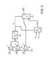
- FIG. 1shows a bit-slice for a data buffer chip that interfaces with DDR DRAMs.
- Data input D(N)is one of 25 or so data lines input to a buffer chip.
- Data input D(N)is compared to a reference voltage Vref by differential buffer 16 , then muxed by mux 22 before being applied to the D-input of flip-flop 20 .
- the Q(N) output of flip-flop 20is a latched data bit that can be applied to one of the DDR DRAM's data inputs.
- Vrefis a reference voltage such as Vcc/2.
- Differential buffers 12 , 14also receive Vref.
- Differential buffer 12compares data strobe input DCS to Vref while differential buffer 14 compares chip-select input CSR to Vref.
- NAND gate 24combines the outputs of differential buffers 12 , 14 and drives the control input to mux 22 through inverter 18 .
- mux 22selects the upper input, recycling the Q(N) output back to the D(N) input of flip-flop 20 .
- mux 22selects its lower input, and the data input D(N) is latched into flip-flop 20 on the next clock edge.
- Clock buffer 26receives a differential clock ICK and ICKB, and generates a clock edge to flip-flop 20 when the differential clock signals cross-over.
- Reset signal RSTcan be applied to differential buffers 12 , 14 , 16 , clock buffer 26 , and flip-flop 20 .
- FIG. 1shows a bit-slice for a data buffer chip that interfaces with DDR DRAMs.
- FIG. 2shows a bit slice of a buffer chip with a reduced data-path delay by removal of the data mux.
- FIG. 3shows the data path of the flip-flop in the data path.
- FIG. 4is a schematic of a clock-locking circuit for the flip-flop in the reduced data path.
- the present inventionrelates to an improvement in buffer chips.
- the following descriptionis presented to enable one of ordinary skill in the art to make and use the invention as provided in the context of a particular application and its requirements.
- Various modifications to the preferred embodimentwill be apparent to those with skill in the art, and the general principles defined herein may be applied to other embodiments. Therefore, the present invention is not intended to be limited to the particular embodiments shown and described, but is to be accorded the widest scope consistent with the principles and novel features herein disclosed.
- the inventorhas realized that data-input-path delays can be reduced if the mux can be eliminated. Since the mux is in the critical path, removal if the mux can reduce propagation delays and allow for a smaller differential input buffer to be used for the data input. The smaller differential buffer can result is a significant power reduction since one differential buffer is need for each of the 25 or so data input slices.
- FIG. 2shows a bit slice of a buffer chip with a reduced data-path delay by removal of the data mux.
- Differential input buffers 12 , 14 , 16compare DCS, CSR, and data input D(N) to reference voltage Vref.
- the output of differential buffer 16is directly applied to the D input of flip-flop 40 , eliminating the mux delay of FIG. 1 .
- Clock buffer 26generates a clock edge to flip-flop 40 when differential clock signals ICK, ICKB cross-over.
- Control logic 30receives the outputs of differential buffer 12 , 14 , and generates chip-select pulse CSP. CSP is driven Control logic 30 drives CSP low when both DCS and CSR are high, or when reset RST is high. Additional mode logic may be included in control logic 30 , such as for interleaving of for bank selection.
- Chip-select pulse CSPis applied to clock buffer 26 and to flip-flop 40 .
- Chip-select pulse CSPcan gate the clock buffer to reduce power consumption.
- Reset signal RSTis applied to flip-flop 40 , control logic 30 , and differential buffers 12 , 14 , 16 .
- FIG. 3shows the data path of the flip-flop in the data path.
- Flip-flop 40receives the data signal D output by differential buffer 16 of FIG. 2 and generates output Q as Q(N).
- a true and complement clock, CK ,CKB, and a reset signal RST,are also input.
- Data signal Dpasses through a first transmission gate of p-channel transistor 54 , which receives CK at its gate, and n-channel transistor 52 , which receives CKB at its gate.
- the first transmission gateis open when CK is low.
- the other side of the first transmission gatedrives the input of inverter 56 , which feeds its output back to the gates of p-channel feedback transistor 44 and n-channel feedback transistor 49 .
- Clock signal CKBis applied to the gate of p-channel clock transistor 46 , which is in series between p-channel feedback transistor 44 and the input of inverter 56 .
- Clock signal CKis applied to the gate of n-channel clock transistor 48 , which is in series between n-channel feedback transistor 49 and the input of inverter 56 .
- Transistors 44 , 46 , 48 , 49are in series and form a clocked inverter.
- the output of inverter 56drives the input of a second transmission gate of n-channel transistor 60 , which receives CK at its gate, and p-channel transistor 62 , which receives CKB at its gate.
- the second transmission gateis open when CK is high. On the rising edge of CK, data from the master stage is passed through the second transmission gate to the slave stage.
- the other side of the second transmission gatedrives an input of NAND gate 50 , which feeds its output back to the gates of p-channel feedback transistor 64 and n-channel feedback transistor 69 .
- Clock signal CKis applied to the gate of p-channel clock transistor 66 , which is in series between p-channel feedback transistor 64 and an input of NAND gate 50 .
- Clock signal CKBis applied to the gate of n-channel clock transistor 68 , which is in series between n-channel feedback transistor 69 and the input of NAND gate 50 .
- Transistors 64 , 66 , 68 , 69are in series and form a second clocked inverter.
- the other input of NAND gate 50is the reset signal RSTB.
- RSTBis driven low to force high the output of flip-flop 40 . This Q output can later be inverted.
- Inverter 58has its input coupled to the drains of transistors 66 , 68 and the output of the second transmission gate. Inverter 58 drives the final output Q of flip-flop- 40 .
- FIG. 4is a schematic of a clock-locking circuit for the flip-flop in the reduced data path.
- NAND gates 90 , 92form a S-R latch receiving CLK, CSP, that drives TCKB
- NOR gates 94 , 96form another S-R latch receiving inverses of CLK, CSP that drives TCK.
- CKis driven high through p-channel transistors 70 , 72 when both TCKB and CLKB are low, or otherwise driven low by either of n-channel transistors 74 , 76 .
- CKBis driven low by n-channel transistors 84 , 86 when both TCK and CLK are high, or otherwise driven high by either of p-channel transistors 80 , 82 .
- inverter 99drives high the lower input of NOR gate 96 , which drives TCLK low regardless of CLKB. This turns on p-channel transistor 80 , which holds CKB high.
- clock-locking circuit 40 ′allows clock CLK to propagate CK, CKB to the data latches of FIG. 3 .
- the high CSPcauses NAND gate 92 to act as an inverter, and through inverter 99 causes NOR gate 96 to also act as an inverter. If CLK is low, then TCKB is low and TCK is high, so CKB is high and CK is low. Then when CLK goes high, TCKB goes high and TCK goes low, causing CKB to go low and CK to go high.
- flip-flop 40When chip-select pulse CSP goes from low to high, flip-flop 40 must not latch new data D. Instead, the old data Q must be maintained. Without using the data-path mux, data can be held by preventing a rising clock edge on CK when CSP goes high and CLK is already high.
- NAND gate 90When CLK is low and CSP goes from low to high, NAND gate 90 continues to output a 1 , allowing TCKB to go low, turning on p-channel transistor 70 . However, since CLKB is high, the state of CK does not change but remains low. NOR gate 94 continues to output a low since CLKB is high, so CSP drives TCK high through NOR gate 96 . N-channel transistor 86 is turned on, but n-channel transistor 84 remains off since CLK is low. Thus the rising transition of CSP is blocked from changing CK, CKB.
- CSPcauses inverter 99 to drive a high to NOR gate 96 , which drives a low to NOR gate 94 . Since CLK is high, inverter 98 drives a second low to the inputs of NOR gate 94 . The output of NOR gate 94 is high, and is driven back to NOR gate 96 , blocking CSP from propagating through to TCK, CKB. Thus whether CLK is high or low, a rising transition of CSP is blocked from changing CK, CKB.
- the data differential buffercan be reduced in size significantly while still meeting the setup time spec. Simulation has shown power reductions of as much as 48%.
- bufferingcould be added to the outputs of the NAND and NOR gates driving CK and CKB, or these gates can be replaced with other logic such as transmission gates and buffers or switch networks.
- a differential clockcould be directly used by the flip-flop. Signals can be active high or active low.
Landscapes
- Logic Circuits (AREA)
- Dram (AREA)
Abstract
Description
Claims (20)
Priority Applications (2)
| Application Number | Priority Date | Filing Date | Title |
|---|---|---|---|
| US10/249,581US6741111B1 (en) | 2003-04-21 | 2003-04-21 | Data register for buffering double-data-rate DRAMs with reduced data-input-path power consumption |
| US10/709,132US6842059B1 (en) | 2003-04-21 | 2004-04-15 | Muxed-output double-date-rate-2 (DDR2) register with fast propagation delay |
Applications Claiming Priority (1)
| Application Number | Priority Date | Filing Date | Title |
|---|---|---|---|
| US10/249,581US6741111B1 (en) | 2003-04-21 | 2003-04-21 | Data register for buffering double-data-rate DRAMs with reduced data-input-path power consumption |
Related Child Applications (1)
| Application Number | Title | Priority Date | Filing Date |
|---|---|---|---|
| US10/709,132ContinuationUS6842059B1 (en) | 2003-04-21 | 2004-04-15 | Muxed-output double-date-rate-2 (DDR2) register with fast propagation delay |
Publications (1)
| Publication Number | Publication Date |
|---|---|
| US6741111B1true US6741111B1 (en) | 2004-05-25 |
Family
ID=32312016
Family Applications (2)
| Application Number | Title | Priority Date | Filing Date |
|---|---|---|---|
| US10/249,581Expired - Fee RelatedUS6741111B1 (en) | 2003-04-21 | 2003-04-21 | Data register for buffering double-data-rate DRAMs with reduced data-input-path power consumption |
| US10/709,132Expired - Fee RelatedUS6842059B1 (en) | 2003-04-21 | 2004-04-15 | Muxed-output double-date-rate-2 (DDR2) register with fast propagation delay |
Family Applications After (1)
| Application Number | Title | Priority Date | Filing Date |
|---|---|---|---|
| US10/709,132Expired - Fee RelatedUS6842059B1 (en) | 2003-04-21 | 2004-04-15 | Muxed-output double-date-rate-2 (DDR2) register with fast propagation delay |
Country Status (1)
| Country | Link |
|---|---|
| US (2) | US6741111B1 (en) |
Cited By (6)
| Publication number | Priority date | Publication date | Assignee | Title |
|---|---|---|---|---|
| US20060248260A1 (en)* | 2003-09-30 | 2006-11-02 | Maksim Kuzmenka | Circuit system |
| US20070081397A1 (en)* | 2005-09-28 | 2007-04-12 | Hynix Semiconductor Inc. | Data output multiplexer |
| US20080005416A1 (en)* | 2006-06-08 | 2008-01-03 | Atmel Corporation | Data register with efficient erase, program verify, and direct bit-line memory access features |
| US8913447B2 (en) | 2011-06-24 | 2014-12-16 | Micron Technology, Inc. | Method and apparatus for memory command input and control |
| CN110297792A (en)* | 2019-08-02 | 2019-10-01 | 深圳市富满电子集团股份有限公司 | Data high level width stablizes forwarding chip and Cascading Methods |
| US20230261649A1 (en)* | 2022-02-11 | 2023-08-17 | Pratt & Whitney Canada Corp. | Logic circuit for providing a signal value after a predetermined time period and method of using same |
Families Citing this family (8)
| Publication number | Priority date | Publication date | Assignee | Title |
|---|---|---|---|---|
| US7126389B1 (en)* | 2004-01-27 | 2006-10-24 | Integrated Device Technology, Inc. | Method and apparatus for an output buffer with dynamic impedance control |
| US7518933B2 (en)* | 2007-02-07 | 2009-04-14 | Freescale Semiconductor, Inc. | Circuit for use in a multiple block memory |
| US7450454B1 (en) | 2007-05-09 | 2008-11-11 | Freescale Semiconductor, Inc. | Low voltage data path in memory array |
| KR100924354B1 (en)* | 2008-04-07 | 2009-11-02 | 주식회사 하이닉스반도체 | Input buffer |
| US7859919B2 (en)* | 2008-08-27 | 2010-12-28 | Freescale Semiconductor, Inc. | Memory device and method thereof |
| US9911470B2 (en)* | 2011-12-15 | 2018-03-06 | Nvidia Corporation | Fast-bypass memory circuit |
| US10141930B2 (en) | 2013-06-04 | 2018-11-27 | Nvidia Corporation | Three state latch |
| CN109738793A (en)* | 2019-01-16 | 2019-05-10 | 华大半导体有限公司 | A kind of analog signal test circuit |
Citations (12)
| Publication number | Priority date | Publication date | Assignee | Title |
|---|---|---|---|---|
| US3764989A (en) | 1972-12-20 | 1973-10-09 | Ultronic Systems Inc | Data sampling apparatus |
| US4539587A (en) | 1983-12-30 | 1985-09-03 | Gte Products Corporation | Shift register driven video measurement system for microcomputer |
| US4744063A (en) | 1983-05-31 | 1988-05-10 | Kabushiki Kaisha Toshiba | Static memory utilizing transition detectors to reduce power consumption |
| US4962487A (en) | 1988-03-31 | 1990-10-09 | Kabushiki Kaisha Toshiba | Static random access memory device with power down function |
| US5189647A (en) | 1991-02-25 | 1993-02-23 | International Business Machines Corp. | Information processing system having power saving control of the processor clock |
| US5404327A (en) | 1988-06-30 | 1995-04-04 | Texas Instruments Incorporated | Memory device with end of cycle precharge utilizing write signal and data transition detectors |
| US5566130A (en) | 1995-11-09 | 1996-10-15 | The United States Of America As Represented By The Secretary Of The Air Force | Address transition detection (ATD) circuit for asynchronous VLSI chips |
| US6049846A (en) | 1990-04-18 | 2000-04-11 | Rambus Inc. | Integrated circuit having memory which synchronously samples information with respect to external clock signals |
| US6204707B1 (en) | 1998-08-26 | 2001-03-20 | Kabushiki Kaisha Toshiba | Flip-flop circuit with clock signal control function and clock control circuit |
| US6304506B1 (en) | 2000-09-25 | 2001-10-16 | United Microelectronics Corp. | Energy-saving device for memory circuit |
| US6404233B1 (en) | 1997-12-11 | 2002-06-11 | Intrinsity, Inc. | Method and apparatus for logic circuit transition detection |
| US6424590B1 (en) | 1999-08-31 | 2002-07-23 | Hitachi, Ltd. | Semiconductor device |
Family Cites Families (11)
| Publication number | Priority date | Publication date | Assignee | Title |
|---|---|---|---|---|
| US5391935A (en) | 1993-07-22 | 1995-02-21 | International Business Machines Corporation | Assertive latching flip-flop |
| US5410194A (en) | 1993-08-11 | 1995-04-25 | Xilinx, Inc. | Asynchronous or synchronous load multifunction flip-flop |
| US5751174A (en) | 1996-08-02 | 1998-05-12 | National Science Council Of Republic Of China | Double edge triggered flip-flop |
| JP3653170B2 (en) | 1998-01-27 | 2005-05-25 | 三菱電機株式会社 | Latch circuit and flip-flop circuit |
| KR100319892B1 (en) | 1999-06-30 | 2002-01-10 | 윤종용 | Method and circuit for latching data line in the data output path of a synchronous semiconductor memory device |
| US6584578B1 (en) | 2000-03-14 | 2003-06-24 | Mosel Vitelic, Inc. | Arbitration method and circuit for control of integrated circuit double data rate (DDR) memory device output first-in, first-out (FIFO) registers |
| US6462596B1 (en) | 2000-06-23 | 2002-10-08 | International Business Machines Corporation | Reduced-transistor, double-edged-triggered, static flip flop |
| US6510100B2 (en) | 2000-12-04 | 2003-01-21 | International Business Machines Corporation | Synchronous memory modules and memory systems with selectable clock termination |
| US6691272B2 (en) | 2000-12-12 | 2004-02-10 | Lsi Logic Corporation | Testing of high speed DDR interface using single clock edge triggered tester data |
| US6535032B2 (en)* | 2001-04-25 | 2003-03-18 | Micron Technology, Inc. | Data receiver technology |
| US6542416B1 (en) | 2001-11-02 | 2003-04-01 | Rambus Inc. | Methods and arrangements for conditionally enforcing CAS latencies in memory devices |
- 2003
- 2003-04-21USUS10/249,581patent/US6741111B1/ennot_activeExpired - Fee Related
- 2004
- 2004-04-15USUS10/709,132patent/US6842059B1/ennot_activeExpired - Fee Related
Patent Citations (12)
| Publication number | Priority date | Publication date | Assignee | Title |
|---|---|---|---|---|
| US3764989A (en) | 1972-12-20 | 1973-10-09 | Ultronic Systems Inc | Data sampling apparatus |
| US4744063A (en) | 1983-05-31 | 1988-05-10 | Kabushiki Kaisha Toshiba | Static memory utilizing transition detectors to reduce power consumption |
| US4539587A (en) | 1983-12-30 | 1985-09-03 | Gte Products Corporation | Shift register driven video measurement system for microcomputer |
| US4962487A (en) | 1988-03-31 | 1990-10-09 | Kabushiki Kaisha Toshiba | Static random access memory device with power down function |
| US5404327A (en) | 1988-06-30 | 1995-04-04 | Texas Instruments Incorporated | Memory device with end of cycle precharge utilizing write signal and data transition detectors |
| US6049846A (en) | 1990-04-18 | 2000-04-11 | Rambus Inc. | Integrated circuit having memory which synchronously samples information with respect to external clock signals |
| US5189647A (en) | 1991-02-25 | 1993-02-23 | International Business Machines Corp. | Information processing system having power saving control of the processor clock |
| US5566130A (en) | 1995-11-09 | 1996-10-15 | The United States Of America As Represented By The Secretary Of The Air Force | Address transition detection (ATD) circuit for asynchronous VLSI chips |
| US6404233B1 (en) | 1997-12-11 | 2002-06-11 | Intrinsity, Inc. | Method and apparatus for logic circuit transition detection |
| US6204707B1 (en) | 1998-08-26 | 2001-03-20 | Kabushiki Kaisha Toshiba | Flip-flop circuit with clock signal control function and clock control circuit |
| US6424590B1 (en) | 1999-08-31 | 2002-07-23 | Hitachi, Ltd. | Semiconductor device |
| US6304506B1 (en) | 2000-09-25 | 2001-10-16 | United Microelectronics Corp. | Energy-saving device for memory circuit |
Cited By (11)
| Publication number | Priority date | Publication date | Assignee | Title |
|---|---|---|---|---|
| US20060248260A1 (en)* | 2003-09-30 | 2006-11-02 | Maksim Kuzmenka | Circuit system |
| US20070081397A1 (en)* | 2005-09-28 | 2007-04-12 | Hynix Semiconductor Inc. | Data output multiplexer |
| US7554857B2 (en)* | 2005-09-28 | 2009-06-30 | Hynix Semiconductor Inc. | Data output multiplexer |
| US20080005416A1 (en)* | 2006-06-08 | 2008-01-03 | Atmel Corporation | Data register with efficient erase, program verify, and direct bit-line memory access features |
| US7580291B2 (en) | 2006-06-08 | 2009-08-25 | Atmel Corporation | Data register with efficient erase, program verify, and direct bit-line memory access features |
| US8913447B2 (en) | 2011-06-24 | 2014-12-16 | Micron Technology, Inc. | Method and apparatus for memory command input and control |
| US9466348B2 (en) | 2011-06-24 | 2016-10-11 | Micron Technology, Inc. | Method and apparatus for memory command input and control |
| CN110297792A (en)* | 2019-08-02 | 2019-10-01 | 深圳市富满电子集团股份有限公司 | Data high level width stablizes forwarding chip and Cascading Methods |
| CN110297792B (en)* | 2019-08-02 | 2024-05-17 | 富满微电子集团股份有限公司 | Data high-level width stable forwarding chip and cascading method |
| US20230261649A1 (en)* | 2022-02-11 | 2023-08-17 | Pratt & Whitney Canada Corp. | Logic circuit for providing a signal value after a predetermined time period and method of using same |
| US12278624B2 (en)* | 2022-02-11 | 2025-04-15 | Pratt & Whitney Canada Corp. | Logic circuit for providing a signal value after a predetermined time period and method of using same |
Also Published As
| Publication number | Publication date |
|---|---|
| US6842059B1 (en) | 2005-01-11 |
Similar Documents
| Publication | Publication Date | Title |
|---|---|---|
| KR100567065B1 (en) | Input circuit for memory device | |
| KR100406543B1 (en) | Pipe-latch control circuit in synchronous memory | |
| KR100543915B1 (en) | Data input device of memory device | |
| US7499343B2 (en) | Data alignment circuit and alignment method for semiconductor memory device | |
| KR100605590B1 (en) | Semiconductor memory device that can adjust impedance of data output driver | |
| US8559247B2 (en) | Dynamic level shifter for interfacing signals referenced to different power supply domains | |
| US6741111B1 (en) | Data register for buffering double-data-rate DRAMs with reduced data-input-path power consumption | |
| KR100919815B1 (en) | Semiconductor memory device | |
| KR101261397B1 (en) | Self reset clock buffer in memory devices | |
| US20040041579A1 (en) | Semiconductor chip test system and test method thereof | |
| US7379376B2 (en) | Internal address generator | |
| US7408394B2 (en) | Measure control delay and method having latching circuit integral with delay circuit | |
| KR100772689B1 (en) | Memory device including a small clock buffer. | |
| US8483005B2 (en) | Internal signal generator for use in semiconductor memory device | |
| CN1248776A (en) | Synchronous semiconductor memory device with clock generating circuit | |
| KR20140146332A (en) | Clock control device | |
| JPH0745075A (en) | Semiconductor integrated circuit | |
| KR20030092506A (en) | Clock driver | |
| KR20170126270A (en) | Data output circuit and semiconductor memory device including the same | |
| US6781919B2 (en) | Address selection circuit and semiconductor memory device with synchronous and asynchronous address signal paths | |
| KR100295682B1 (en) | Data input buffer circuit | |
| US6195296B1 (en) | Semiconductor memory device and system | |
| US6819134B2 (en) | Decoding circuit for wafer burn-in test | |
| US7120083B2 (en) | Structure and method for transferring column address | |
| US7894276B2 (en) | Apparatus and methods for an input circuit for a semiconductor memory apparatus |
Legal Events
| Date | Code | Title | Description |
|---|---|---|---|
| AS | Assignment | Owner name:PERICOM SEMICONDUCTOR CORP., CALIFORNIA Free format text:ASSIGNMENT OF ASSIGNORS INTEREST;ASSIGNOR:WU, KE;REEL/FRAME:013651/0265 Effective date:20030502 | |
| FEPP | Fee payment procedure | Free format text:PAT HOLDER NO LONGER CLAIMS SMALL ENTITY STATUS, ENTITY STATUS SET TO UNDISCOUNTED (ORIGINAL EVENT CODE: STOL); ENTITY STATUS OF PATENT OWNER: LARGE ENTITY | |
| FPAY | Fee payment | Year of fee payment:4 | |
| FPAY | Fee payment | Year of fee payment:8 | |
| AS | Assignment | Owner name:BANK OF AMERICA, N.A., AS ADMINISTRATIVE AGENT, TE Free format text:SECURITY INTEREST;ASSIGNOR:PERICOM SEMICONDUCTOR CORPORATION, AS GRANTOR;REEL/FRAME:037255/0122 Effective date:20151209 | |
| REMI | Maintenance fee reminder mailed | ||
| LAPS | Lapse for failure to pay maintenance fees | ||
| STCH | Information on status: patent discontinuation | Free format text:PATENT EXPIRED DUE TO NONPAYMENT OF MAINTENANCE FEES UNDER 37 CFR 1.362 | |
| FP | Lapsed due to failure to pay maintenance fee | Effective date:20160525 | |
| AS | Assignment | Owner name:DIODES INCORPORATED, TEXAS Free format text:ASSIGNMENT OF ASSIGNORS INTEREST;ASSIGNOR:PERICOM SEMICONDUCTOR CORPORATION;REEL/FRAME:044975/0554 Effective date:20171222 | |
| AS | Assignment | Owner name:BANK OF AMERICA, N.A., AS ADMIN. AGENT, NORTH CAROLINA Free format text:SECURITY AGREEMENT;ASSIGNOR:DIODES INCORPORATED;REEL/FRAME:045195/0446 Effective date:20180122 Owner name:BANK OF AMERICA, N.A., AS ADMIN. AGENT, NORTH CARO Free format text:SECURITY AGREEMENT;ASSIGNOR:DIODES INCORPORATED;REEL/FRAME:045195/0446 Effective date:20180122 |