US6740853B1 - Multi-zone resistance heater - Google Patents
Multi-zone resistance heaterDownload PDFInfo
- Publication number
- US6740853B1 US6740853B1US10/088,504US8850402AUS6740853B1US 6740853 B1US6740853 B1US 6740853B1US 8850402 AUS8850402 AUS 8850402AUS 6740853 B1US6740853 B1US 6740853B1
- Authority
- US
- United States
- Prior art keywords
- heater
- gas
- quartz
- quartz plate
- plate
- Prior art date
- Legal status (The legal status is an assumption and is not a legal conclusion. Google has not performed a legal analysis and makes no representation as to the accuracy of the status listed.)
- Expired - Fee Related
Links
- 238000010438heat treatmentMethods0.000claimsabstractdescription113
- 238000001816coolingMethods0.000claimsabstractdescription107
- 239000000758substrateSubstances0.000claimsabstractdescription90
- 238000012545processingMethods0.000claimsabstractdescription57
- 239000007789gasSubstances0.000claimsdescription174
- 239000010453quartzSubstances0.000claimsdescription127
- VYPSYNLAJGMNEJ-UHFFFAOYSA-Nsilicon dioxideInorganic materialsO=[Si]=OVYPSYNLAJGMNEJ-UHFFFAOYSA-N0.000claimsdescription127
- 239000002826coolantSubstances0.000claimsdescription71
- 239000000463materialSubstances0.000claimsdescription38
- 229910000953kanthalInorganic materials0.000claimsdescription25
- 229910045601alloyInorganic materials0.000claimsdescription19
- 239000000956alloySubstances0.000claimsdescription19
- PNEYBMLMFCGWSK-UHFFFAOYSA-Naluminium oxideInorganic materials[O-2].[O-2].[O-2].[Al+3].[Al+3]PNEYBMLMFCGWSK-UHFFFAOYSA-N0.000claimsdescription14
- BASFCYQUMIYNBI-UHFFFAOYSA-NplatinumChemical compound[Pt]BASFCYQUMIYNBI-UHFFFAOYSA-N0.000claimsdescription12
- QVGXLLKOCUKJST-UHFFFAOYSA-Natomic oxygenChemical compound[O]QVGXLLKOCUKJST-UHFFFAOYSA-N0.000claimsdescription11
- 238000000151depositionMethods0.000claimsdescription11
- 238000004519manufacturing processMethods0.000claimsdescription11
- 239000000203mixtureSubstances0.000claimsdescription11
- 239000001301oxygenSubstances0.000claimsdescription11
- 229910052760oxygenInorganic materials0.000claimsdescription11
- 230000001681protective effectEffects0.000claimsdescription11
- XEEYBQQBJWHFJM-UHFFFAOYSA-NIronChemical compound[Fe]XEEYBQQBJWHFJM-UHFFFAOYSA-N0.000claimsdescription10
- 238000005530etchingMethods0.000claimsdescription9
- 125000006850spacer groupChemical group0.000claimsdescription9
- 230000008878couplingEffects0.000claimsdescription8
- 238000010168coupling processMethods0.000claimsdescription8
- 238000005859coupling reactionMethods0.000claimsdescription8
- 229910052782aluminiumInorganic materials0.000claimsdescription7
- XAGFODPZIPBFFR-UHFFFAOYSA-NaluminiumChemical compound[Al]XAGFODPZIPBFFR-UHFFFAOYSA-N0.000claimsdescription7
- 230000008021depositionEffects0.000claimsdescription7
- ZOKXTWBITQBERF-UHFFFAOYSA-NMolybdenumChemical compound[Mo]ZOKXTWBITQBERF-UHFFFAOYSA-N0.000claimsdescription6
- 238000005520cutting processMethods0.000claimsdescription6
- 239000011733molybdenumSubstances0.000claimsdescription6
- 229910052750molybdenumInorganic materials0.000claimsdescription6
- 229910052697platinumInorganic materials0.000claimsdescription6
- XLYOFNOQVPJJNP-UHFFFAOYSA-NwaterSubstancesOXLYOFNOQVPJJNP-UHFFFAOYSA-N0.000claimsdescription6
- VYZAMTAEIAYCRO-UHFFFAOYSA-NChromiumChemical compound[Cr]VYZAMTAEIAYCRO-UHFFFAOYSA-N0.000claimsdescription5
- 229910052804chromiumInorganic materials0.000claimsdescription5
- 239000011651chromiumSubstances0.000claimsdescription5
- 229910017052cobaltInorganic materials0.000claimsdescription5
- 239000010941cobaltSubstances0.000claimsdescription5
- GUTLYIVDDKVIGB-UHFFFAOYSA-Ncobalt atomChemical compound[Co]GUTLYIVDDKVIGB-UHFFFAOYSA-N0.000claimsdescription5
- 229910052742ironInorganic materials0.000claimsdescription5
- 230000000284resting effectEffects0.000claimsdescription4
- 229910001080W alloyInorganic materials0.000claimsdescription3
- 239000004020conductorSubstances0.000claimsdescription3
- 238000000227grindingMethods0.000claimsdescription3
- HBMJWWWQQXIZIP-UHFFFAOYSA-Nsilicon carbideChemical compound[Si+]#[C-]HBMJWWWQQXIZIP-UHFFFAOYSA-N0.000claimsdescription3
- 229910010271silicon carbideInorganic materials0.000claimsdescription3
- 230000015572biosynthetic processEffects0.000claimsdescription2
- 238000003698laser cuttingMethods0.000claimsdescription2
- 238000007789sealingMethods0.000claims16
- 229910052751metalInorganic materials0.000claims4
- 239000002184metalSubstances0.000claims4
- 239000000112cooling gasSubstances0.000claims1
- 238000013021overheatingMethods0.000claims1
- 238000009826distributionMethods0.000abstractdescription37
- 238000013461designMethods0.000abstractdescription16
- 235000012431wafersNutrition0.000description112
- 238000012546transferMethods0.000description43
- 238000000034methodMethods0.000description29
- 239000010410layerSubstances0.000description27
- 239000012530fluidSubstances0.000description16
- 230000008569processEffects0.000description13
- 239000004065semiconductorSubstances0.000description9
- 230000005855radiationEffects0.000description8
- 230000007423decreaseEffects0.000description7
- 230000006870functionEffects0.000description7
- 230000004044responseEffects0.000description7
- 230000000694effectsEffects0.000description6
- 239000012212insulatorSubstances0.000description6
- XUIMIQQOPSSXEZ-UHFFFAOYSA-NSiliconChemical compound[Si]XUIMIQQOPSSXEZ-UHFFFAOYSA-N0.000description5
- 230000001419dependent effectEffects0.000description5
- 230000004907fluxEffects0.000description5
- 230000009467reductionEffects0.000description5
- 230000002829reductive effectEffects0.000description5
- 239000010703siliconSubstances0.000description5
- 229910052710siliconInorganic materials0.000description5
- 238000004458analytical methodMethods0.000description4
- 238000013459approachMethods0.000description4
- 238000003754machiningMethods0.000description4
- TWNQGVIAIRXVLR-UHFFFAOYSA-Noxo(oxoalumanyloxy)alumaneChemical compoundO=[Al]O[Al]=OTWNQGVIAIRXVLR-UHFFFAOYSA-N0.000description4
- 239000012298atmosphereSubstances0.000description3
- 230000008901benefitEffects0.000description3
- 238000005094computer simulationMethods0.000description3
- 238000009792diffusion processMethods0.000description3
- 239000001307heliumSubstances0.000description3
- 229910052734heliumInorganic materials0.000description3
- SWQJXJOGLNCZEY-UHFFFAOYSA-Nhelium atomChemical compound[He]SWQJXJOGLNCZEY-UHFFFAOYSA-N0.000description3
- 229910001120nichromeInorganic materials0.000description3
- 229920002120photoresistant polymerPolymers0.000description3
- UQSXHKLRYXJYBZ-UHFFFAOYSA-NIron oxideChemical compound[Fe]=OUQSXHKLRYXJYBZ-UHFFFAOYSA-N0.000description2
- PXHVJJICTQNCMI-UHFFFAOYSA-NNickelChemical compound[Ni]PXHVJJICTQNCMI-UHFFFAOYSA-N0.000description2
- WYTGDNHDOZPMIW-RCBQFDQVSA-NalstonineNatural productsC1=CC2=C3C=CC=CC3=NC2=C2N1C[C@H]1[C@H](C)OC=C(C(=O)OC)[C@H]1C2WYTGDNHDOZPMIW-RCBQFDQVSA-N0.000description2
- 239000000969carrierSubstances0.000description2
- 230000015556catabolic processEffects0.000description2
- 238000006243chemical reactionMethods0.000description2
- 230000003247decreasing effectEffects0.000description2
- 238000006731degradation reactionMethods0.000description2
- 230000004927fusionEffects0.000description2
- 239000011810insulating materialSubstances0.000description2
- 238000005259measurementMethods0.000description2
- 230000007246mechanismEffects0.000description2
- 238000012986modificationMethods0.000description2
- 230000004048modificationEffects0.000description2
- 230000001590oxidative effectEffects0.000description2
- 238000000059patterningMethods0.000description2
- 230000007723transport mechanismEffects0.000description2
- 238000005303weighingMethods0.000description2
- 238000013316zoningMethods0.000description2
- OKTJSMMVPCPJKN-UHFFFAOYSA-NCarbonChemical compound[C]OKTJSMMVPCPJKN-UHFFFAOYSA-N0.000description1
- 229910000640Fe alloyInorganic materials0.000description1
- -1HastaloySubstances0.000description1
- 229910001182Mo alloyInorganic materials0.000description1
- 239000000853adhesiveSubstances0.000description1
- 230000001070adhesive effectEffects0.000description1
- 230000002411adverseEffects0.000description1
- CYUOWZRAOZFACA-UHFFFAOYSA-Naluminum ironChemical compound[Al].[Fe]CYUOWZRAOZFACA-UHFFFAOYSA-N0.000description1
- 230000000712assemblyEffects0.000description1
- 238000000429assemblyMethods0.000description1
- 230000004888barrier functionEffects0.000description1
- 230000005540biological transmissionEffects0.000description1
- 238000009835boilingMethods0.000description1
- 239000007767bonding agentSubstances0.000description1
- 229910052799carbonInorganic materials0.000description1
- 238000003486chemical etchingMethods0.000description1
- 238000005229chemical vapour depositionMethods0.000description1
- VNNRSPGTAMTISX-UHFFFAOYSA-Nchromium nickelChemical compound[Cr].[Ni]VNNRSPGTAMTISX-UHFFFAOYSA-N0.000description1
- 239000002131composite materialSubstances0.000description1
- 238000007906compressionMethods0.000description1
- 230000006835compressionEffects0.000description1
- 238000011109contaminationMethods0.000description1
- 230000008602contractionEffects0.000description1
- 239000010432diamondSubstances0.000description1
- 229910003460diamondInorganic materials0.000description1
- 239000002019doping agentSubstances0.000description1
- 238000005553drillingMethods0.000description1
- 238000009429electrical wiringMethods0.000description1
- 238000001704evaporationMethods0.000description1
- 230000008020evaporationEffects0.000description1
- 238000009472formulationMethods0.000description1
- 239000011521glassSubstances0.000description1
- 238000009616inductively coupled plasmaMethods0.000description1
- 238000002329infrared spectrumMethods0.000description1
- 150000002500ionsChemical class0.000description1
- 230000000670limiting effectEffects0.000description1
- 239000004973liquid crystal related substanceSubstances0.000description1
- 230000008018meltingEffects0.000description1
- 238000002844meltingMethods0.000description1
- 229910001092metal group alloyInorganic materials0.000description1
- 229910052759nickelInorganic materials0.000description1
- 229910000623nickel–chromium alloyInorganic materials0.000description1
- 229910052756noble gasInorganic materials0.000description1
- 150000002835noble gasesChemical class0.000description1
- 230000003647oxidationEffects0.000description1
- 238000007254oxidation reactionMethods0.000description1
- 230000036961partial effectEffects0.000description1
- 230000002093peripheral effectEffects0.000description1
- 230000036581peripheral resistanceEffects0.000description1
- 239000000843powderSubstances0.000description1
- 238000002360preparation methodMethods0.000description1
- 238000004321preservationMethods0.000description1
- 239000011241protective layerSubstances0.000description1
- 238000005086pumpingMethods0.000description1
- 230000001105regulatory effectEffects0.000description1
- 230000000630rising effectEffects0.000description1
- 238000000926separation methodMethods0.000description1
- 230000035939shockEffects0.000description1
- 238000001228spectrumMethods0.000description1
- 230000032258transportEffects0.000description1
Images


Classifications
- H—ELECTRICITY
- H01—ELECTRIC ELEMENTS
- H01L—SEMICONDUCTOR DEVICES NOT COVERED BY CLASS H10
- H01L21/00—Processes or apparatus adapted for the manufacture or treatment of semiconductor or solid state devices or of parts thereof
- H01L21/67—Apparatus specially adapted for handling semiconductor or electric solid state devices during manufacture or treatment thereof; Apparatus specially adapted for handling wafers during manufacture or treatment of semiconductor or electric solid state devices or components ; Apparatus not specifically provided for elsewhere
- H01L21/67005—Apparatus not specifically provided for elsewhere
- H01L21/67011—Apparatus for manufacture or treatment
- H01L21/67098—Apparatus for thermal treatment
- H01L21/67109—Apparatus for thermal treatment mainly by convection
- C—CHEMISTRY; METALLURGY
- C23—COATING METALLIC MATERIAL; COATING MATERIAL WITH METALLIC MATERIAL; CHEMICAL SURFACE TREATMENT; DIFFUSION TREATMENT OF METALLIC MATERIAL; COATING BY VACUUM EVAPORATION, BY SPUTTERING, BY ION IMPLANTATION OR BY CHEMICAL VAPOUR DEPOSITION, IN GENERAL; INHIBITING CORROSION OF METALLIC MATERIAL OR INCRUSTATION IN GENERAL
- C23C—COATING METALLIC MATERIAL; COATING MATERIAL WITH METALLIC MATERIAL; SURFACE TREATMENT OF METALLIC MATERIAL BY DIFFUSION INTO THE SURFACE, BY CHEMICAL CONVERSION OR SUBSTITUTION; COATING BY VACUUM EVAPORATION, BY SPUTTERING, BY ION IMPLANTATION OR BY CHEMICAL VAPOUR DEPOSITION, IN GENERAL
- C23C16/00—Chemical coating by decomposition of gaseous compounds, without leaving reaction products of surface material in the coating, i.e. chemical vapour deposition [CVD] processes
- C23C16/44—Chemical coating by decomposition of gaseous compounds, without leaving reaction products of surface material in the coating, i.e. chemical vapour deposition [CVD] processes characterised by the method of coating
- C23C16/458—Chemical coating by decomposition of gaseous compounds, without leaving reaction products of surface material in the coating, i.e. chemical vapour deposition [CVD] processes characterised by the method of coating characterised by the method used for supporting substrates in the reaction chamber
- C23C16/4582—Rigid and flat substrates, e.g. plates or discs
- C23C16/4583—Rigid and flat substrates, e.g. plates or discs the substrate being supported substantially horizontally
- C23C16/4586—Elements in the interior of the support, e.g. electrodes, heating or cooling devices
- C—CHEMISTRY; METALLURGY
- C23—COATING METALLIC MATERIAL; COATING MATERIAL WITH METALLIC MATERIAL; CHEMICAL SURFACE TREATMENT; DIFFUSION TREATMENT OF METALLIC MATERIAL; COATING BY VACUUM EVAPORATION, BY SPUTTERING, BY ION IMPLANTATION OR BY CHEMICAL VAPOUR DEPOSITION, IN GENERAL; INHIBITING CORROSION OF METALLIC MATERIAL OR INCRUSTATION IN GENERAL
- C23C—COATING METALLIC MATERIAL; COATING MATERIAL WITH METALLIC MATERIAL; SURFACE TREATMENT OF METALLIC MATERIAL BY DIFFUSION INTO THE SURFACE, BY CHEMICAL CONVERSION OR SUBSTITUTION; COATING BY VACUUM EVAPORATION, BY SPUTTERING, BY ION IMPLANTATION OR BY CHEMICAL VAPOUR DEPOSITION, IN GENERAL
- C23C16/00—Chemical coating by decomposition of gaseous compounds, without leaving reaction products of surface material in the coating, i.e. chemical vapour deposition [CVD] processes
- C23C16/44—Chemical coating by decomposition of gaseous compounds, without leaving reaction products of surface material in the coating, i.e. chemical vapour deposition [CVD] processes characterised by the method of coating
- C23C16/46—Chemical coating by decomposition of gaseous compounds, without leaving reaction products of surface material in the coating, i.e. chemical vapour deposition [CVD] processes characterised by the method of coating characterised by the method used for heating the substrate
- H—ELECTRICITY
- H01—ELECTRIC ELEMENTS
- H01L—SEMICONDUCTOR DEVICES NOT COVERED BY CLASS H10
- H01L21/00—Processes or apparatus adapted for the manufacture or treatment of semiconductor or solid state devices or of parts thereof
- H01L21/67—Apparatus specially adapted for handling semiconductor or electric solid state devices during manufacture or treatment thereof; Apparatus specially adapted for handling wafers during manufacture or treatment of semiconductor or electric solid state devices or components ; Apparatus not specifically provided for elsewhere
- H01L21/67005—Apparatus not specifically provided for elsewhere
- H01L21/67011—Apparatus for manufacture or treatment
- H01L21/67098—Apparatus for thermal treatment
- H01L21/67103—Apparatus for thermal treatment mainly by conduction
- H—ELECTRICITY
- H01—ELECTRIC ELEMENTS
- H01L—SEMICONDUCTOR DEVICES NOT COVERED BY CLASS H10
- H01L21/00—Processes or apparatus adapted for the manufacture or treatment of semiconductor or solid state devices or of parts thereof
- H01L21/67—Apparatus specially adapted for handling semiconductor or electric solid state devices during manufacture or treatment thereof; Apparatus specially adapted for handling wafers during manufacture or treatment of semiconductor or electric solid state devices or components ; Apparatus not specifically provided for elsewhere
- H01L21/683—Apparatus specially adapted for handling semiconductor or electric solid state devices during manufacture or treatment thereof; Apparatus specially adapted for handling wafers during manufacture or treatment of semiconductor or electric solid state devices or components ; Apparatus not specifically provided for elsewhere for supporting or gripping
- H01L21/6831—Apparatus specially adapted for handling semiconductor or electric solid state devices during manufacture or treatment thereof; Apparatus specially adapted for handling wafers during manufacture or treatment of semiconductor or electric solid state devices or components ; Apparatus not specifically provided for elsewhere for supporting or gripping using electrostatic chucks
Definitions
- the present inventionrelates generally to a multi-purpose wafer holder for holding a wafer (or other substrate) during processing in a plasma system. More specifically, the holder includes at least one stacked layer to provide clamping, conduction, heating and/or cooling. Examples of layers include an electrostatic chuck, a multi-zone He gas delivery system, a multi-zone resistance heater, and a multi-zone cooling system.
- resistance heatersto heat a semiconductor wafer that is in the presence of a processing gas. Heating alters the characteristics of the reaction process occurring on the semiconductor wafer.
- Such resistance heatershave been used within quasi-hot wall, or warm wall, reactors where the resistance heater serves as the support for the silicon wafer and simultaneously heats the wafer to carry out a predetermined processing step.
- a processing gas of a predetermined purity and/or pressureis circulated over the heated silicon wafer to modify the surface characteristics of the silicon wafer.
- Chemical vapor depositionis one environment in which such resistance heaters are used to process semiconductor wafers.
- Such resistance heatershave typically employed heating elements of (1) a nickel-chromium alloy (nichrome) or (2) an aluminum-iron alloy, which are electrically resistive and which generate heat when an electrical current is applied through the elements.
- a nickel-chromium alloynichrome
- an aluminum-iron alloywhich are electrically resistive and which generate heat when an electrical current is applied through the elements.
- Examples of commercially available materials commonly used to fabricate resistive heating elements employed in ovensare Kanthal, Nikrothal and Alkrothal, which are registered trademark names for metal alloys produced by Kanthal Corporation of Bethel, Conn.
- the Kanthal familyincludes ferritic alloys (FeCrAl) and the Nikrothal family includes austenitic alloys (NiCr, NiCrFe).
- resistance heater elementshave not, in the past, been exposed to the processing gas that is circulated over the silicon wafer within the reactor. Moreover, large heater elements with large thermal masses have been required to provide a barrier of material between the wafer and the heater elements when heating in known plasma systems.
- Known electrically resistive materialssuch as some of the Kanthal alloys, require an oxygenated environment for long element life. The presence of oxygen causes an aluminum oxide to form upon the surface of a Kanthal alloy heater element which inhibits evaporation of the heater element. An acceptable level of oxygen is 5% of 760 torr with no other gases which react to the alloy surface. Alternatively, environments with less oxygen can cause the oxide layer to become porous and allows iron oxide to migrate along grain boundaries, causing contamination of the system.
- the heater elements of wafer processing systemsalso have had thermal masses that are significantly greater than the wafer or substrate that they have heated.
- heater elements weighing tens of poundshave been used to heat wafers weighing only two ounces.
- the heaterhas a pronounced lateral profile which heats a wafer much more in the center region than compared to the edge region of the wafer.
- complicated devices having on the order of 30 partswere used in known systems to adjust the applied heat.
- a large thermal massalso leads to a high thermal inertia—an effect where the heater element continues to apply heat to the wafer (or other substrate) after the wafer has already achieved its desired temperature.
- radial or lateral heat transferhas been higher than in the substrate being processed, making it harder to isolate changes in temperature in the wafer.
- the present inventionrelates to a stack of elements onto which a substrate (e.g., a wafer or an LCD panel) can be placed during a series of one or more plasma or thermal processing steps.
- the types of elements in the stackinclude, but are not limited to: an electrostatic clamp (either single- or multi-zone), a He gas delivery system (either single- or multi-zone), a resistance heater (either single- or multi-zone), and/or a cooling system (either single- or multi-zone).
- At least one of the elementsis selected based on the processing step(s) to be performed.
- Each elementis hermetically sealed from each other element and from the processing environment. Accordingly, one embodiment of the present invention acts as more than one of: an electrostatic chuck with electrostatic clamping, a resistance heater, and a cooling system.
- an electrostatic chuckwhich clamps a substrate thereto and enables the clamping of the substrate to be measured.
- first and second electrodesare housed internal to the electrostatic chuck and clamp the substrate to the chuck. The capacitance between the first and second electrodes is measured after the substrate is applied to the chuck to determine the effective clamping of the substrate.
- plural sealed platesare used together to provide pressure control for an He gas delivery system on the back side of the substrate in a plasma processing chamber.
- the Helium gas delivery systemprovides He to the back side of a substrate at a pressure significantly greater than the chamber (processing) pressure (i.e., typically 30-50 Torr) in order to improve the conduction of heat between the substrate and the chuck. Electrically clamping the substrate to the chuck enables using a back side gas pressure substantially greater then the chamber pressure.
- the area of the substrate and chuckare smooth enough that they provide a good gas seal.
- the He gas delivery systemis zoned to provide different amounts of He to different parts of the substrate in order to match a conduction profile of the substrate.
- the He gas delivery systemmay be used in combination with the above-described electrostatic chuck.
- the electrostatic chuckincludes gas holes and the He gas delivery system is placed below the electrostatic chuck. The He gas then passes through the holes in the electrostatic chuck to provide conduction to the wafer.
- the gas conductionvaries directly with pressure (e.g., up to 15 torr).
- a resistance heaterfor heating a semiconductor wafer within a wafer processing reactor.
- the heaterincludes a resistance heater element disposed in a heater channel formed in one or more quartz plates.
- One embodiment of the resistance heaterincludes heater channels with supply end head room to accommodate expansion and contraction of the heater element which occurs during heating and cooling.
- the quartz plates forming the housing for the resistance heaterare fused together at plural adjoining surfaces and preferably at all adjoining surfaces.
- the resistance heater elementis secured therebetween to form a gas-tight chamber.
- a sufficient number of fusion pointsare provided to prevent the internal pressure of the resistance heater from popping the fusion points when in the reduced pressure atmosphere of the plasma processing chamber.
- Electrical terminals coupled to the resistance heater elementare provided for conducting electrical current.
- a gas ductis connected to the gas-tight chamber formed between the quartz plates for admitting gas(es) of predetermined composition(s) and pressure(s) thereto independent of the composition and pressure of the processing gas circulating about the external face of the wafer holder.
- the resistance heater elementis formed of a material such as a Kanthal alloy or platinum, since those materials can be heated in air without damage.
- a sheet of materialmay be melted, drawn, chemically etched, sputtered, laser cut, cut with a water jet, or otherwise shaped to form a resistance heater element matching the heat transfer characteristics of the element to be heated.
- one or more wires of one or more of the above materialsmay be used as the heater element.
- the quartz platesare constructed to have features matching the heater elements. The features, when fused together, provide a hermetic seal to separate the processing environment from the gas over the conductor. The seals must reliably accommodate the ultra-high temperatures of the heater.
- the thermal transfer characteristicsare examined using at least one of the three disclosed techniques.
- changes in an LCD paperare examined when the LCD paper is applied to a previously uniformly heated substrate which is placed on an electrostatic chuck. Photographs of the changes in the paper indicate the shape of the heat loss of the heated substrate.
- an infrared scanner or detectormeasures the changes in heat emissions across the surface of a previously heated substrate as it cools on the chuck.
- One such detector that monitors spatially and temporally evolving temperature in the absence of a plasmais a commercially available wafer instrumented with thermocouples (e.g., SensArray Corporation, Model No. 1530A).
- the transfer characteristics of a substrate on a chuckare simulated by a computer based on the shapes and thermal characteristics of the substrates to be heated and the shape and heat transfer characteristics of the chuck on which the substrate is heated.
- a set of cooling platesfor one or more of: (1) cooling a substrate before processing, (2) maintaining a cool temperature of the substrate during processing and (3) cooling the substrate after processing is complete.
- One embodiment of the cooling systemis a multi-zone cooling system that cools a substrate according to a heat loss characteristic of the substrate. By applying coolant more rapidly in areas that would otherwise cool more slowly, the substrate is more uniformly cooled. Also, by reducing the substrate temperature quickly after processing, any temperature-based reactions are more effectively halted at a process end-point.
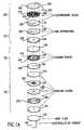
- FIG. 1Ais a cross-section of a complete wafer holder implementing a stack of a multi-zone electrostatic chuck, a multi-zone He gas distribution system, a multi-zone resistance heater, and multi-zone cooling system;
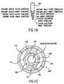
- FIG. 1Bis a side view of a first electrical/fluid conduit for passing electrical connections, gas, and coolant to the different layers shown in FIG. 1A;
- FIG. 1Cis a cross section of a second electrical/fluid conduit for passing the electrical connections, the gas, and the coolant to the different layers shown in FIG. 1A;
- FIG. 1Dis a cross section of a third electrical/fluid conduit for passing the electrical connections, the gas, and the coolant to the different layers shown in FIG. 1A;
- FIG. 1Eis a cross section of a fourth electrical/fluid conduit for passing the electrical connections, the gas, and the coolant to the different layers shown in FIG. 1A;
- FIG. 1Fis a top view of a focus ring on top of the layers of the wafer holder
- FIG. 1Gis a top view of the focus ring combined with the layers of FIG. 1F;
- FIG. 1His a cross-section showing how sections can be separately formed with individual cover and base plates for each section;
- FIG. 11is a top view of a focus ring on top of the wafer holder implemented using the individual sections of FIG. 1H;
- FIG. 2is a cross-section of a cooled electrostatic chuck including an He gas distribution system underneath a multi-electrode electrostatic chuck;
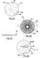
- FIG. 3Ais a top view of a top plate of an electrostatic chuck according to a first embodiment
- FIG. 3Bis a top view of a middle plate of the electrostatic chuck according to a first embodiment
- FIG. 3Cis a cross section of the middle plate of the electrostatic chuck according to a first embodiment
- FIG. 3Dis a top view of a bottom plate of the electrostatic chuck according to a first embodiment
- FIG. 3Eis a cut-away top view of an electrostatic chuck according to a second embodiment
- FIG. 4Ais a top view of a top plate of an He gas delivery system according to a first embodiment
- FIG. 4Bis a top view of a middle plate of the He gas delivery system according to a first embodiment
- FIG. 4Cis a cross section of the middle plate of the He gas delivery system according to a first embodiment
- FIG. 4Dis a top view of a bottom plate of the He gas delivery system according to a first embodiment
- FIG. 4Eis a cross section of the bottom plate of FIG. 4D according to a first embodiment
- FIG. 4Fis a cutaway top view of a He gas distribution system according to a second embodiment
- FIG. 4Gis a top view of a plate of the He gas distribution system according to the second embodiment.
- FIG. 4His a cutaway top view of a He gas distribution system according to a third embodiment
- FIG. 5Ais a top view of a top plate of an electrical resistance heater
- FIG. 5Bis a top view of a middle plate of an electrical resistance heater having an inner zone and an outer zone according to a first implementation
- FIG. 5Cis a top view of a bottom plate of an electrical resistance heater
- FIG. 6Ais a top view of a top plate of an electrical resistance heater
- FIG. 6Bis a top view of a middle plate of an electrical resistance heater having an inner zone and an outer zone according to a second implementation
- FIG. 6Cis a top view of a bottom plate of an electrical resistance heater
- FIG. 6Dis an expanded top view of a portion of the middle plate according to the second implementation.
- FIG. 6Eis a cross section of a portion of the inner zone of the middle plate according to the second implementation.
- FIG. 7Ais a schematic illustration of a five-part heater according to a third implementation
- FIG. 7Bis a schematic illustration of a four-part heater according to a fourth implementation
- FIG. 7Cis a schematic illustration of a eight-part heater according to a fifth implementation.
- FIG. 7Dis a schematic illustration of a five-part heater according to a sixth implementation.
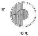
- FIG. 7Eis a schematic illustration of a five-part heater according to a seventh implementation.
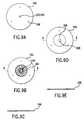
- FIG. 8Ais a schematic illustration of a wire heating element within a substantially square channel
- FIG. 8Bis a schematic illustration of a strip heating element within a substantially rectangular channel
- FIG. 8Cis a schematic illustration of a wire heating element within a square channel with a regular pattern of quartz/channel/quartz/channel;
- FIG. 8Dis a schematic illustration of a wire heating element within a substantially circular channel
- FIG. 8Eis a schematic illustration of a wire heating element resting on supports within a channel
- FIG. 8 F( 1 )is a schematic illustration of a strip heating element resting on tabs within a substantially rectangular channel
- FIG. 8 F( 2 )is a front view cross-section of the tabs on which a strip heating element rests when the strip is within a substantially rectangular channel;
- FIG. 8 F( 3 )is a side view of the tabs on which a strip heating element rests when the strip is within a substantially rectangular channel;
- FIG. 8Gis a schematic illustration of a wire heating element within a square channel with a regular pattern of quartz/channel/quartz/channel;
- FIG. 8His a schematic illustration of a bent, variable width wire heating element
- FIG. 8Iis an enlargement of a section of a heater element
- FIG. 8Jis an enlargement of a wire lead attaching to a wire heater element within a channel
- FIG. 9Ais a top view of a top plate of a cooling system according to a first implementation
- FIG. 9Bis a top view of a second plate of the cooling system according to a first implementation.
- FIG. 9Cis a cross section of the second plate of the cooling system shown in FIG. 9B;
- FIG. 9Dis a top view of a third plate of the cooling system according to a first implementation.
- FIG. 9Eis a cross section of the third plate of the cooling system shown in FIG. 9D;
- FIG. 9Fis a top view of a fourth plate of the cooling system according to a first implementation.
- FIG. 9Gis a cross section of the fourth plate of the cooling system shown in FIG. 9F;
- FIG. 9His a top view of a fifth plate of the cooling system according to a first implementation.
- FIG. 9Iis a cross section of the fifth plate of the cooling system shown in FIG. 9H;
- FIG. 10Ais a top view of a top plate of a cooling system according to a second implementation
- FIG. 10Bis a top view of a second plate of a cooling system according to the second implementation.
- FIG. 10Cis a cross section of the second plate of the cooling system shown in FIG. 10B;
- FIG. 10Dis a top view of a third plate of a cooling system according to the second implementation.
- FIG. 10Eis a cross section of the third plate of the cooling system shown in FIG. 10D including a reflective material and a thermal insulator coupled to the bottom of the third plate;
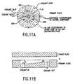
- FIG. 11Ais a top view of coolant strips within a multi-zone cooling section
- FIG. 11Bis a cross-section of a cooling strip of the cooling strips of FIG. 11A;
- FIG. 12is a schematic illustration of an oven for forming the substrate holder from the individual plates or separate sections
- FIG. 13is a side view of the focus ring and substrate holder in a plasma processing environment
- FIG. 14is a schematic illustration of a substrate holder including a circular inner region surrounded by annular rings, wherein coolant is fed to separate channels that spiral radially outward;
- FIG. 15is a schematic illustration of a heating plate that can be lifted off of the cooling plate.
- FIGS. 16A through 16Dillustrate methods of manufacturing layers of the present invention.
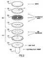
- FIG. 1Aillustrates a preferred embodiment of a stack of elements.
- the stackoperates as a combined electrostatic chuck 102 , He distribution system 122 , electrical resistance heater 132 , and cooling assembly 152 , in accordance with the present invention.
- the first three plates ( 100 , 105 , and 110 )comprise the electrostatic chuck 102
- the next two plates ( 120 and 125 )comprise the He gas distribution system 122
- the next three plates ( 130 , 135 , and 140 )comprise the electrical resistance heater 132
- the last five plates( 145 , 150 , 155 , 160 , and 165 ) comprise the cooling system 152 .
- plural platesare combined to form one or more “super-plates” with the same functionality as the plates which the super-plates replace.
- the bottom-most plate 110 of the electrostatic chuck 102can be combined with the top plate 120 of the He gas distribution system.
- the bottom plate 125 of the He gas distribution system 122can be combined with the top plate 130 of the electrical resistance heater 132 . All thirteen plates are stacked concentrically on top of each other and rest on a base plate 170 attached to an electrical/fluid conduit 180 .
- zonesare arranged concentrically. Each zone transports at least one of an electrical signal, a gas, and a coolant to the various layers.
- zonesare arranged from an exterior to an interior in an order as follows: coolant outlet-outer zone 200 , coolant outlet-inner zone 205 , coolant inlet-outer zone 210 , coolant inlet-inner zone 215 , heating plate-outer zone 220 , heating plate-inner zone 225 , He gas outer zone 230 , He gas-inner zone 235 , electrostatic chuck electrical wiring-outer zone 240 , and electrostatic chuck electrical inner zone 245 .
- the embodiment shownis only exemplary, and the order of the inner and outer zones and the order of the inlets and outlets can be changed without departing from the spirit of the present invention.
- FIG. 1Cshows a second implementation of the electrical/fluid conduit 180 that is used in conjunction with additional inlets and outlets shown in FIG. 10 E.
- the electrical conduits for the inner zone 245 and the outer zone 240 of the electrostatic chuck 102are combined with the inner zone 225 and the outer zone 220 of the heating plate 132 to form an electrical conduit 181 .
- the remainder of the conduit 180includes an inner ring 175 and an outer ring 173 .
- the inner ringincluding notches 176 and 178 , forms two conduits for the He gas outer zone 230 and the He gas-inner zone 235 .
- the outer ring 173forms conduits for the coolant outlet-inner zone 205 and the coolant inlet-inner zone 215 .
- additional structural rigidityis achieved because each inner conduit attaches to an outer conduit.
- the internal ribbingalso enables proper alignment of the concentric conduits, sites for fusing adjacent conduits, and an improved ducting for coolant and gas flow.
- each ring 173 and 175may be rotated such that the notches are at different angles with respect to each other.
- each ringcan be divided into a smaller number of hermetically sealed sections to accommodate a different number of zones for each of the layers. For example, if three He gas supply regions are used in the He gas distribution system 122 , then the inner ring 175 would contain three sections instead of the illustrated two.
- the conduit 180is implemented as a bundle of tubes grouped together.
- the tubesmay be (1) constant size throughout the conduit 180 or (2) may increase in volume and be realigned as tubes are no longer needed higher in the stack of quartz plates.
- payloade.g., coolant
- the conduitssmaller conduits may be contained within larger conduits.
- a structure similar to FIG. 1Dmay itself be enclosed in a circular conduit, creating the configuration of FIG. 1 E.
- Each of the plates shown in FIG. 1Aare formed of a thermally conductive but electrically insulating layer (e.g., quartz) and are joined to the corresponding conduit structures in FIGS. 1B-1E using “frit” as a bonding agent.
- the wiresare run through the conduits, and then the frit is placed on the plates around the holes and at each adjacent edge between plates.
- a dopantis placed in ground quartz to lower its melting temperature.
- the portions to be bondedare then assembled under mechanical pressure in a kiln and are fired in air to a temperature sufficient to melt the doped quartz. As the peripheral portions of the doped quartz melt, they become fused together and form a gas-tight seal.
- Quartz fusing processesare known to those skilled in the art of quartz processing. As is discussed in greater detail with reference to FIG. 12, if the bonding is performed in a sleeve, then the concentric alignment is more easily maintained. This alignment sleeve feature can be supplemented or replaced with an array of alignment pins. Although this design is described as made of quartz and diffusion bonded, it could also be made of other material such as alumina and glass frit bonding. One of ordinary skill in the art will recognize that other insulating and bonding materials may be used without departing from the spirit of the invention.
- FIG. 1AThe structure of FIG. 1A is shown in FIG. 1F in a condensed form.
- a focus ring 900is shown which consistently aligns the wafer of the chuck and affects the edge plasma over the wafer 190 .
- the focus ring 900 and substrate holder of FIG. 1Fform a completed structure as shown in FIG. 1 G.
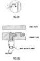
- one or more of the series of plates forming a sectionare formed independently and include a cover plate, a primary plate and a base plate, as shown in FIG. 1 H.
- the primary plateis formed with a series of channels or grooves to accommodate the elements (e.g., heating elements and capacitive elements) or carriers (e.g., gases or coolants) placed in the channels or grooves.
- the cover and base platesare utilized to keep the elements and carriers in the channels or grooves.
- each of the sectionscan be used as a separate “stand-alone” component by using the cover plate, the primary plate and the base plate. That is, any one section could be attached to the electrical/fluid conduit and combined with the focus ring if the processing environment only required one function (e.g., (1) heating without cooling and clamping or (2) clamping without heating or cooling).
- the geometry of the substrate in semiconductor processingis circular and therefore the chuck geometry described herein will be cylindrical with the following primary dimensions shown in FIG. 1 I.
- the geometry of the chuckis not limited to a cylindrical geometry.
- the chuckcan be described by its radius R and its height H.
- the height of the chuckwill be a function of the components included within its design and their respective thicknesses.
- FIG. 11illustrates these thicknesses as well as a preferred order of arrangement for each of the sections.
- the radius R of the chuckis greater than the radius of the wafer r w in order to provide space for a focus ring that allows for repeatable placement of the wafer (or substrate) upon the chuck.
- FIG. 1Gshows the dimensions in relation to each other.
- the radius of the chuckcan be scaled according to the size of the substrate to be processed (e.g., 8 and 12 inch diameters).
- the zone patternhas a radius substantially equivalent to the radius of the substrate.
- the chuck baseserves as a structural base to the chuck components and can also act as a manifold wherein all electrical wiring, coolant and gas can be distributed to their respective component destinations.
- the wafer holderincludes only a subset of the plates shown in FIG. 1 A.
- the wafer holderonly implements an electrostatic chuck and an He gas distribution system on top of the base plate.
- the electrical/fluid conduitaccordingly only contains a subset of the conduits shown in FIGS. 1B-1D.
- Other assembliesare possible, such as a heater 132 with an He gas distribution system 122 .
- the plate 100becomes part of the He gas distribution system 122 and is sealed above plate 120 .
- the order of the assemblyis dictated by the most important functions to be accomplished. For example, if cooling is more important than heating, then the order of the heating assembly 132 is switched with the cooling assembly 152 to ensure that the cooling function is closest to the substrate.
- an electrostatic chuck 102includes plates 100 , 105 , and 110 , which act as a first, a second, and a third plate, respectively, and which are shown in FIGS. 3A-3D.
- the first plate 100includes (1) lift pin through-holes 300 for enabling the wafer to be lifted off the chuck and (2) gas distribution through-holes 305 for coupling a gas to the back of a wafer 190 . In alignment with these through-holes on the first plate 100 are similar through-holes 300 and 305 in the second and third plates ( 105 and 110 ).
- plate 100may be grooved on the wafer side to further distribute the Helium gas.
- first and second electrostatic gripping elementsalso formed in the second plate 105 is two concentric channels 310 and 315 into which first and second electrostatic gripping elements (or simply “electrodes”) are placed.
- the first and second electrostatic gripping elementsprovide electrostatic coupling to a wafer 190 when a wafer is present on the wafer holder.
- the strength of the hold of an electrostatic chuck on the wafercan be indirectly determined by measuring the capacitance between the wafer and the first and second electrostatic gripping elements when the wafer 190 is placed on the wafer holder. If the wafer 190 is not held correctly by the electrostatic chuck 102 , then a warning can be signaled to the operator to reseat the wafer 190 . Alternatively, the wafer 190 may be automatically reseated if an automatic wafer handling system is used. In either case, the signal may act to prevent starting a process which requires that the wafer be tightly held.
- FIG. 3Cshows a cross section of the second plate 105 and illustrates that the channels do not extend the entire depth of the plate 105 . This allows the electrostatic gripping elements on top to be electrically isolated from the wires underneath as they pass through the conduit 180 .
- the wirespass underneath the second plate 105 in an electrical groove 320 shown in FIG. 3 D.
- the wirespass up from the conduit using zones 240 and 245 .
- the channels 310 and 315can also be formed in the top plate 100 with the second plate being formed with a flat top.
- FIG. 3Eis a cut-away top view of an electrostatic chuck according to a second embodiment.
- the five zonesare divided into an inner zone surrounded by four outer zones.
- the inner zonelikewise could be split into four sub-zones thereby forming concentric quadrants.
- Each electrostatic gripping elementis isolated and can be maintained at its own separate voltage.
- the electrostatic chuck zoningmay be either unipolar or bipolar (alternating sign of potential between adjacent gripping elements). In both cases, electrostatic forces are used to clamp the substrate (e.g., a wafer) to the chuck.
- the electrostatic gripping elementsare configured for a parallel line element such that the element spires are aligned above the quartz separating the heating elements shown in FIGS. 7D and 7E.
- the heating elementsare visible below the electrostatic plate. Therefore, the heating elements can directly “see” the wafer and provide radiative heat transfer. Furthermore, the electrostatic gripping elements may heat up and radiate to the wafer effectively increasing the radiating area. However, this effect is believed to be small.
- the leads to the individual electrostatic gripping elementsare shown in FIG. 3 E. These may coincide with the He gas feed-throughs used for the He gas distribution plate. Exemplary lift pin holes 300 are also shown.
- the primary plate thickness, Hcan be thin, e.g., approximately 1 mm or 40 mil.
- zonesare shown in FIG. 3E, it would be evident to one of ordinary skill in the art that additional zones can be formed in an alternate embodiment.
- the zonesmay either be concentric, form quadrants, form concentric quadrants, or any combination thereof.
- FIG. 3Eshows a preferred embodiment.
- the zonesmay be formed as a set of strips of any selected pattern required to provide uniform coupling.
- the electrostatic gripping elementsare seated within quartz channels.
- a very thick quartz platemay be used to encase the elements within the quartz.
- clearance in the electrostatic gripping element channelsis necessary to accommodate the different coefficients of thermal expansion between the gripping elements and the quartz (when heating applications are exercised, the gripping elements and surrounding quartz are likely to heat up to temperatures substantially greater than the ambient temperature).
- FIGS. 4A-4Eone embodiment of a gas distribution system 122 is illustrated.
- He gasis distributed.
- other gasespreferably noble gases, are distributed.
- FIG. 4Ashows that the top plate of the electrostatic chuck 102 is moved down into the gas distribution system 122 when the electrostatic chuck 102 is not used.
- the through-holes 300 and 305 in these platesare aligned concentrically with the through-holes in the electrostatic chuck 102 .
- the hole 235e.g., a counter-bore
- the holes 305 A and 305 Bthere are sixty-four holes ( 305 A and 305 B)in the top plate 100 extending radially in eight lines.
- FIGS. 4B-4Ethe separation of the gas distribution system 122 into two zones is illustrated. Gas passes through the gas-inner zone 235 and spreads into the entire gas distribution-inner zone 330 bounded by ring 331 . As shown in FIG. 4C, the inner zone 330 is about half of the depth of the plate 120 . The gas in zone 330 is forced out through one of the inner thirty-two through-holes 305 A which are above the circle bounded by ring 331 .
- the second zoneis supplied by a gas-outer zone 230 which fills into the gas distribution outer zone 335 shown in FIG. 4 D.
- the outer zone 335is shown in FIG. 4E as being half of the depth of the plate 125 .
- the portion of the conduit 180 that acts as the gas-outer zone 230ends underneath the fifth plate 120 , and only the gas-inner zone 235 continues above.
- the gas that passes to a higher layer from this layerpasses via one of the thirty-two outer through-holes 305 B.
- the flow rates (and gas types) for each zonemay be modified to adjust the pressure field (and conduction) between the wafer and the wafer holder within the two radial zones.
- the radial distribution of the heat transfer coefficientmay be varied to vary the radial distribution of the conductive-convective heat flux.
- FIG. 4Fis a cutaway top view of a He gas distribution system according to a second embodiment.
- FIG. 4Gillustrates the primary plate for the He gas distribution component.
- the thickness H2 of the He gas distribution platecan be small, i.e., less than 1 mm or 40 mil total.
- FIGS. 4F and 4Hillustrate two different He gas shower head designs.
- This platemay serve as the cover plate of the chuck below the focus ring. It simply serves the purpose of passing the gas to the backside of the wafer.
- the embodiment of FIG. 4Futilizes a radial design
- the embodiment of FIG. 4Hillustrates a preferred, parallel line design.
- the parallel lines of the gas holesare interweaved between electrostatic gripping elements.
- the electrostatic component and the He gas distribution componentare used (if He gas is used, an electrostatic component or other mechanical gripping element must be used to counter the gas pressure on the backside of the wafer), then the arrangement will be as shown in FIG. 1 F. This means that the hole distribution shown in FIG.
- the He gas distribution plateis placed below the electrostatic plate such that the distance between the electrostatic plate and the wafer is minimal, hence, maximizing the electrostatic coupling.
- the division of the zonesmay also be accomplished externally to the wafer holder itself.
- the gas passing through holes 305 A and 305 Bare fed by separate inlets 480 and 490 that extend from the top to the bottom of the wafer holder (i.e., throughout the entire wafer holder down to a manifold). Gas lines coupled to the bottom of the inlets 480 and 490 then provide gas to individual holes or groups of holes. These inlets 480 and 490 may also serve as the electrical conduits for the electrostatic gripping elements.
- This approachprovides the finest-grain control of conduction since each hole or group of holes can be controlled separately. This approach, however, requires the most care in the preparation of the quartz plates such that the holes 305 A and 305 B do not interfere with the routing of heating elements or cooling channels described below.
- the resistance heater shown in FIGS. 5A-5Cis designated generally by reference numeral 132 and includes a generally central resistance heater element channel 340 and a surrounding peripheral resistance heater element channel 345 .
- central resistance heater element channel 340has an outer periphery substantially commensurate with the inner periphery of a surrounding annular array or elements.
- the resistance heater elements for the channels 340 and 345are connected to wires passing through the electrical/fluid conduit 180 .
- the channelsare cut into (or otherwise formed in) an upper surface of the eighth quartz plate 135 .
- the channelsmay be formed in the under surface of the seventh plate 130 .
- the thickness of the quartz plateis selected to provide sufficient mechanical strength to resist pressure differentials between the resistance heater element and the low pressure processing area. However, the thickness is balanced by (1) a need to provide maximum heat transfer through the plates 130 and 135 and (2) a desire to have a reduced thermal mass and inertia. Such heat is primarily transferred by radiation and conduction, depending upon the temperature and material properties of the surfaces. In these configurations, with highly resistive materials it is possible to achieve a 5-25 kW heater (dependent upon the chuck diameter or wafer diameter, i.e., 5 to 12 inch wafer diameter).
- a groove 355is supplied in the ninth plate 140 into which are placed the wires coupling the resistance heater elements in the channels 340 and 345 .
- FIGS. 7C through 7Eillustrate alternative zoning as compared with FIG. 5 B.
- FIG. 7Eis preferred since it provides adjustment and control of properties both in the radial and azimuthal directions.
- itconsists of 5 zones, however, it may be more wherein greater radial or azimuthal resolution can be provided. For instance, it is generally desirable to have greater radial resolution at the wafer edge to compensate for edge loss.
- FIG. 5Billustrates a design that adds the additional constraint that the adjustment and/or control is axisymmetric (no azimuthal adjustment).
- the zonesconsist of rings—illustratively two concentric rings. Again, the number may be increased to provide greater resolution in the radial direction.
- the present inventionis not restricted to the zone patterning of the aforementioned designs. In fact, the patterning can be some complex formulation of surface areas so as to compensate for gross non-uniformities in the processed substrate. On such example is illustrated in FIG. 7 C.
- the channels 340 and 345 of FIG. 5Bare replaced by channels 340 ′ and 345 ′ which cover about 80% of the surface area of the wafer holder.
- An enlarged view of these channelsis shown in FIG. 6 D.
- Another alternativeis to make the grooves by using two plates. One plate is the bottom of the groove and the second is cut completely through to be a spacer between the elements. Bonding the two plates provide the same cross section as described in FIG. 6 E. These channels are significantly larger than those of FIG. 5 B.
- the design of the element surface areais dictated by maximizing the radiative heat transfer of the heating element to the adjacent quartz plate and the silicon wafer. In this embodiment, the depth of the channels versus the distance between channels must be regulated.
- the width of each quartz finger 361is at least as large as a thickness of the quartz remaining after a channel is formed therein. This provides good tensile strength to withstand the internal loads due to expansion of the quartz.
- the heat transport mechanisms for heating the waferinclude: (1) conduction through the entire assembly between the heating element and the wafer, (2) radiation exchange between the heating element and the wafer, and (3) conduction between the adjacent heating element and the quartz followed by radiative exchange between the quartz and the wafer. Although additional heat transport mechanisms may exist, the three described methods are the most significant. In addition, the number of zones and their spatial distribution can be altered without departing from the spirit of the present invention.
- the resistance heater elementsare serpentine; however, in an alternate embodiment, non-serpentine shapes are used, e.g., V-shapes and U-shapes with square edges as opposed to rounded edges.
- channels 340 ′ and 345 ′extend generally parallel to adjacent trailing and leading segments thereof. For example, segment 340 A extends generally parallel to adjacent segment 340 B.
- the heating section of the present inventionlike any of the other sections of the substrate holder can be implemented in the five-zone configuration as shown in FIG. 7A or in a set of concentric zones as shown in FIG. 7 B.
- the inner zone of FIG. 7Acould further be divided into quadrants or quadrants with an inner zone. That is, the five zones (A 1 -A 5 ) of FIG. 7A can be incorporated into a larger inner zone A 1 .
- the shapecan be defined recursively down to a smallest inner zone that is either completely controlled or controlled by quadrants without a separate inner zone.
- Each of the widths of the quadrants in the radial directionneed not be the same size.
- each of the zonesneed not be the same size.
- the width of each zone in the radial directionmay vary, with larger or smaller zones near the edge as compared to near the center. This configuration has less individual control than the corresponding design of FIG. 7A when FIG. 7A is implemented to have an equal number of rings, each broken into four quadrants.
- FIGS. 7C-7EThree additional designs are shown in FIGS. 7C-7E.
- the heating elementsare connected at an edge of the corresponding quadrant.
- the layout of the heating sectionincludes layout and material considerations not only radially, but also into the plane of the heating section.
- FIGS. 8A-8Gillustrate that the type of heating element and its corresponding channel also affect the resultant heat transfer.
- the heating elementcan be: (1) a wire in a substantially square channel (as shown in FIG. 8 A), (2) a wire in a substantially circular channel (as shown in FIG. 8 D), (3) a rectangular strip in a substantially rectangular channel (as shown in FIG.
- the stripis substantially square and resting in a substantially square channel of commensurate size.
- FIG. 8Cillustrates a conservative design criteria for the dimensions of the channels that are machined into the primary plate to house the heating element.
- the illustrated channelhas a depth and width d with sufficient clearance for a heating element having a diameter of approximately d.
- the spacing between elements, the thickness of the cover plate, and the remaining thickness of the primary plateshould be a distance d (hence, the primary plate has a thickness of 2 d ).
- FIGS. 8E and 8Fpresent a wire and strip heating element, respectively, that have “tabs” spaced along their length.
- the “tabs”simply minimize the contact area between the heating element and the quartz (or other material) that houses the heating element. Since the coefficient of thermal expansion of the heating element is greater than that of quartz (by approximately a factor of twenty), the heating element may be prone to moving around. The tabs can help it stay in place wherein the bends in the housing channels, shown in FIG. 8H, can accommodate the thermal growth of the heating element.
- FIG. 8Hrepresents a 180 degree bend in the heating element. If the channel is nominally 1 mm in thickness, then the thickness within the bend may be 1.5 to 2 mm to accommodate element growth. For example, a 1 m long heating element, that is heated to a temperature 1000 degrees above room temperature, can be expected to grow approximately 1 cm (this distance may be distributed equally between all of the bends).
- the heater element channelsare very large such that the elements may move around when heated and hence minimize any stresses in the heating element due to contact with the quartz encasement. Furthermore, the larger volumes to machine demand less complex machining. There are, however, some disadvantages. If the channels are simply made larger than those described above, the frontal surface area of the heating element may be sacrificed. Secondly, if a hollowed volume is used, the movement of the element may cause shorting of the element.
- FIG. 8Gillustrates an example of actual dimensions for the cover plate and primary plate of a heating component. All major dimensions are approximately 1 mm (or 40 mil). Therefore, the use of this heating element in a multiple component chuck would result in a thickness H 3 of 2 mm (or 80 mil) as shown in FIG. 1 I.
- FIG. 8Iillustrates the intersection of three zones (in particular, the center zone and two outer zones) and provides some dimensions for the spacing of the elements in separate zones. Note, that these are conservative dimensions. They may be reduced to improve the thermal response of the plate and maintain structural integrity.
- FIG. 8Jpresents a partial cross-section of the heating component including the primary plate and the cover plate. In particular, it shows an enlarged view of the point where a lead to the heating element passes from the heating component (primary plate) into the structure below.
- high pressure airoxygen
- High pressuremay simply mean atmospheric pressure (which is high relative to the vacuum pressure).
- the passage of air (or oxygen) through the annulus surrounding the heating elementcan serve two purposes. Firstly, the presence of oxygen adjacent to the Kanthal surface can cause oxidation of aluminum that diffuses to the surface of a Kanthal alloy comprising iron, aluminum, chromium, carbon and cobalt. The resultant layer of aluminum oxide can protect the heating element and prolong its lifetime.
- the aluminum oxide layerhas good emission properties in the IR spectrum of interest.
- the airis forced through the annulus it can be used as an additional means of quickly cooling the heating element upon turning off the power to the element. Using forced convection, one can remove residual heat within the heating element, hence, improving the overall response of the cooling system.
- the heating element channel for each zoneis its own separate closed loop both electrically and fluid mechanically. Therefore, the power and/or air flow rate may be varied between zone.
- a shaped resistance heater elementmay be formed by a number of different methods. Laser and water jet cutting are good methods of cutting the desired heater element pattern.
- a sheet of electrically resistive materialis patterned into the serpentine-shape and etched (e.g., chemically or with a laser or water) to provide a resulting structure having the desired serpentine-shape.
- the preferred materialdepends on the desired temperature range of operation, the conditions under which the element must operate, and the sheet size and thickness of the substrate to be heated. Platinum can be used in non-oxidizing environments while nichrome can be used in oxidizing environments. Nickel is useful in low temperature environments, and plated molybdenum is also effective when it is not cost-prohibitive.
- the preferred Kanthal alloyis comprised of aluminum, chromium, cobalt, and iron. Such material is resistive to degradation at high temperatures provided that a protective layer of aluminum oxide is maintained over the surface thereof. To facilitate the formation and preservation of such protective oxide layer, a gas duct is used to admit oxygen into the chamber formed between the seventh and eighth plates 130 and 135 , irrespective of the pressure and gas content surrounding the wafer holder.
- the seventh plate 130is split into a circle and a concentric ring.
- the outer edge of the circleis fused to the inner edge of ring 343
- the concentric ringis fused to (1) an outside of ring 343 at an interior edge and (2) an inside of plate 135 at an exterior edge.
- the circle and the concentric ringare bonded laterally instead of vertically.
- the present inventionalso provides for cooling a wafer quickly using a cooling system 152 .
- Plates 145 , 150 , 155 , 160 , and 165are combined into a cooling system which distributes coolant into an interior zone and an exterior zone through coolant inlets 215 and 210 , respectively.
- the coolant for the inner zoneis moved from the inlet 215 to a corresponding outlet 205 through coolant channel 360 .
- the coolant for the outer zoneis moved from the inlet 210 to a corresponding outlet 200 through coolant channel 370 .
- the inlet and outlet coolant conduitshave been placed concentrically at the center of the wafer holder.
- the plates 150 , 155 , 160 , and 165can be replaced by two plates 162 and 167 shown in FIGS. 10B and 10C.
- coolant from the inner inlet 215passes through inner zone cooling channels 360 and into inner zone exit ring 380 .
- the coolantis then forced down through holes 214 and expelled out the outlet zone 205 (shown in FIG. 1 E).
- coolant for the outer zonearrives through inlet 430 (in FIG. 10E) and passes upward through the holes 211 (shown in FIG. 10 D).
- the coolantthen passes through channels 213 and is forced back down through holes 212 .
- the coolantis then collected in the ring 440 below (shown in FIG. 10E) and exits via outlet 420 .
- the inner and outer cooling zonesare placed in the same plane for more uniform cooling efficiency.
- Plates 400 and 410are thermal insulating materials that have a reflective material for the spectra of radiation of the elements. Those materials help to prevent thermal conduction into the conduit 180 .
- the coolant inlets 430 and outlets 420 for the outer zoneare directly coupled to a cooling manifold below the cooling assembly 152 rather than passing through the conduit 180 .
- the cooling in each zonecan be separately adjusted by independently varying the coolant type and the coolant flow rate.
- the coolant flow rateis directly related to the heat transfer coefficient. However, while varying the coolant flow rate, one changes the pressure drop through the cooling line. Therefore, if one wished to increase the cooling, one could increase the flow rate, however, you would suffer a greater pressure drop.
- the heat transfer coefficientis dependent upon the thermal conductivity, density, specific heat (constant pressure), velocity, viscosity, and (weakly) the hydraulic diameter of the flow duct. For a given coolant, there is only the velocity and the hydraulic diameter (where the velocity gives you the greatest return since it is almost a one-to-one linear relationship).
- the pressure drop through the lineis dependent upon the density, the friction factor (function of the Reynolds number), duct length, hydraulic diameter, and velocity (in fact, it is proportional to the velocity squared).
- FIG. 11Apresents the primary plate for a multi-zone cooling component.
- coolant fluidflows radially outward from inlet holes to outlet holes as shown.
- coolant fluidis fed to the inner zone radial spindles from a center annular conduit.
- the coolant inlets and outletsare connected with appropriate distribution and reception channels within the chuck base.
- the flow path for a specific zonesis a closed loop that is externally connected with a coolant reservoir, heat exchanger and pump that is employed to circulate coolant through the cooling ducts. This way, the coolant temperature, coolant type and flow rate may be varied between zone to produce the desired spatial cooling characteristics.
- FIG. 11Bpresents a cross-section of an outer zone radial spindle, indicated by the letter A in FIG. 11 A.
- the respective coolant inlet and outletare shown wherein the channel depth at the inlet might be h and the channel depth at the outlet might be h′. Since the width of the radial spindle increases as one moves radially outward (shown in FIG. 11 A), the channel depth may be decreased from h to h′ in order to maintain the same channel cross-sectional area.
- the constant areamaintains a constant flow velocity. If the depth is maintained constant, then the increase in area would result in a decrease of the flow velocity, hence, leading to a decrease in the heat transfer coefficient.
- the flow velocitydecreases by a factor of two
- the heat transfer coefficientdecreases by a factor of two
- the wetted perimeterincreases by approximately 20%. Consequently, for a given ⁇ r and ⁇ T, the heat flux decreases by a factor of two, and the heat transfer rate for a radial section decreases by nearly a factor of two.
- the coolant flow channelsare maintained throughout with an approximately constant cross-sectional area.
- the sum of the cross-sectional areas of the inlets, the sum of the cross-sectional areas for the cooling channels and the sum of the cross-sectional areas of the outletsare approximately equivalent. This enables a constant, nearly uniform flow throughout.
- a second order effect in this caseis the slight reduction in the hydraulic diameter with radius which also increases the heat transfer coefficient (only slightly). These two effects are necessary to aid in achieving a constant heat flux with radius (an increase in the heat transfer coefficient can balance the increase in the coolant temperature).
- An alternate embodimentincludes a decreasing cross-sectional area of the channel with increasing radius. This produces an increase in the heat flux (relative to the constant area case) as one moves out radially.
- the cooling channelsmay be designed to produce a variety of cooling effects (in particular radial variation).
- the thickness H 4 of the primary plate for the cooling componentwill generally be greater than other components.
- the cooling channelscan be as large as 4 mm thick and 1 cm wide. This would lead to a conservative thickness H 4 for the primary plate of 1 cm.
- a substrate of the shape and thickness to be processedis uniformly heated in an oven up to the operating temperature at which the substrate will be heated on the chuck.
- the heated waferis then placed on the chuck and a piece of liquid crystal display (LCD) paper is applied to the heated wafer, since the color of the LCD paper changes with temperature.
- Photographsare taken of the LCD paper as it cools, and the color of the LCD paper is thus observed/recorded to observe/record temperature changes.
- the photographs of the cooling processshow the inverse of how the substrate will need heat applied. That is, in rapid heat loss areas, extra heat will need to be applied to maintain the substrate at a uniform temperature compared to the rest of the substrate.
- the heater elementis shaped so that additional coils are placed underneath the rapidly cooling areas of the substrate.
- the same heat analysiscan be performed using an infrared detector to detect changes in the temperature of the substrate as it cools.
- the sampled heat valuescan be displayed on a computer to show how heat is dissipated from the substrate as it cools.
- This methodhas the advantage of measuring a substrate that has a more accurate thermal conduction and radiation since it is the actual substrate. In addition, this substrate and measurement can operate at higher temperatures than expected in actual processing. Thirdly, this method can be operated in the actual gas environment of the process.
- a computeris utilized to simulate the heat transfer characteristic based on a computerized model of the substrate and the chuck on which the substrate will be heated.
- the computer simulationcan factor in a thickness of a substrate, a thickness of the quartz, and expected ambient temperatures of the processing chamber.
- the best methodis to compare computer simulations to infrared measurements and improve the errors in the computer simulations until it is truly predictive.
- a chuck componentThere are two primary steps to the manufacturing of a chuck component (and ultimately the chuck). These two components may be described as (i) machining individual plates, and (ii) adhering (or fusing together) adjacent plates.
- the preferred embodimentdescribes the building of a chuck using quartz (of course if this chuck is to be used in certain etch environments, different material(s) will be required).
- One environment in which a quartz chuck can be usedis in an ash or strip chamber wherein the process is such that the photoresist is removed (or stripped) from the substrate.
- the step of machiningcan consist of several substeps. It may include cutting grooves or channels, drilling holes, or simply cutting the general shape of the plate. Upon cutting the shape of the plate, machining holes, grooves or channels can be performed by any one or combination of the following: (i) water or laser cutting, (ii) using diamond grinding bits, and (iii) chemically etching. For example, one can mask (with photoresist) a pattern and etch the channels.
- the step of fusing plates togethercan be performed as shown in FIG. 12 .
- FIG. 12presents an oven wherein a heat input Q is applied.
- the plates to be fused togetherare set on an oven support that includes a cylindrical alignment ring used to align adjacent plates.
- the primary plateis set down first, the heating element is inserted, the frit is applied to the surfaces intended to be fused, and the cover plate (or adjacent plate) is placed above. These two plates, as indicated in FIG. 12, are then loaded with a uniform force distributed across the upper surface.
- the frit that is used to adhere adjacent platesis primarily comprised of fine quartz powder mixed within an adhesive (to ease application).
- the ovenis heated to and soaked at a temperature of 1050° C. for approximately 1 hour, and then cooled. Upon fusing the adjacent plates, they may be removed and tested for leak integrity. Illustrative methods of manufacturing are illustrated in FIGS. 16A through 16D.
- the electrodes to serve as the electro-static chuck or the heater elementscan be fabricated by patterned deposition, or blanket deposition and patterned etch back.
- the quartz piecesmay be fabricated using either patterned deposition of photo-resist upon blanket deposition (CVD) of doped quartz upon quartz and etching, or patterned deposition (CVD) of doped quartz upon quartz and patterned etch back.
- CVDphoto-resist upon blanket deposition
- CVDpatterned deposition
- FIGS. 16B, 16 C and 16 Dprovide a pictorial description of such a fabrication technique.
- FIG. 16Bpresents two alternatives to fabricate the heater elements set atop a thin quartz plate.
- FIG. 16Cpresents one method of fabricating the plate counterpart with channels in the quartz and doped quartz at the bonding surfaces.
- FIG. 16Dpresents the final step of diffusion bonding two pieces.
- the featuresmay alternatively have rounded surfaces from the etching and deposition of materials. In summary, using such techniques can enable sub-millimeter (or smaller) features.
- FIG. 13illustrates the primary heat transfer paths within the process environment of a plasma processing device.
- the deviceis an inductively coupled plasma chamber used for stripping photoresist from a substrate or wafer.
- the chamberis surrounded by a helical coil and an electrostatic shield.
- a plasmais generated by inductively coupling RF power to the chamber.
- the chuckis illustrated in exaggerated proportions to show a focus ring, heating component, cooling component and chuck base.
- the waferas shown, sits atop the chuck. Starting from the bottom, the chuck base services the heating and cooling components with electrical lines, coolant loops, forced air loops (for the heating element), etc.
- the cooling componentsits above the chuck base. Coolant flows into, throughout and out of the cooling component. The coolant cools the cooling plate and in turn cools the above structure when coolant is flowing. Heat transfer between the coolant and the cooling plate takes place via forced convection (a conductive-convective heat transfer). The heat that is convected away from the chuck via the coolant is exchanged with a cold water supply in a heat exchanger.
- an insulatorIn between the cooling component and the chuck base resides an insulator (with a thermal conductivity significantly lower than that of the remaining chuck structure, i.e., an insulating material or a sealed low pressure gas environment where the heat flow between the two chuck components is restricted to an outer ring that is a material with a low thermal conductivity) and a redundant IR reflecting material.
- the insulatorminimizes heat flow from the chuck base into the cooling component via conduction (important when the system is in a cooling mode).
- the IR reflecting materialreflects any thermal radiation to the chuck base.
- the heating componentsits above the cooling component. Again, an insulator and an IR reflecting material are placed between the components.
- the insulatorserves two purposes: (1) it produces a large ⁇ T across the interface between the heating component and the cooling component (providing effective cooling without coolant boiling at the channel surfaces), and (2) it improves the thermal response of the heating component, i.e., the thermal inertia of the heating plate is reduced since it does not lose as much heat to the cooling plate which is a large heat sink in this case even when the coolant is not flowing.
- the adverse effectis that the insulator will hinder the effectiveness of the cooling plate. Therefore, there is an optimal design for this layer. Also, the forced air over the heating element during cool down will improve the cooling response.
- Heatis exchanged between the heating component and the cooling component via conduction.
- the heating componentheats the wafer via two modes of heat transfer. They are conduction heat transfer and radiation heat transfer. At low heating element temperatures (e.g., 300 degrees C.), the conduction heat transfer is dominant. Above this temperature, radiation heat transfer plays a greater role. In particular, heating the Kanthal element to 1000 degrees C. quickly can enable heating the wafer quickly by means of thermal radiation.
- the wafersits on top of the chuck.
- the conduction between the chuck and the waferis limited by the contact between the two surfaces.
- the heat transfer between the gapsis improved with the use of electrostatic gripping elements and applying the gas to the backside of the wafer.
- the waferis also heated by the plasma. Energy is delivered to the wafer surface during the impact of ions at the surface.
- the wafercan radiatively exchange heat between itself and the chamber walls.
- an insulating layercan be placed between the heating plate and the cooling plate which affects the thermal response of a heating/cooling system.
- One alternative to this configurationis to use a system with a variable heat conductance between the heating plate and the cooling plate.
- the heat transfer coefficient his dependent upon the quality of contact between the two surfaces. It is true that at higher pressures the heat transfer coefficient is directly related to the gas conductivity and inversely related to the thickness of the gas layer, however, it becomes more complicated at lower pressures.
- one embodimentemploys a variable spacing in order to optimally control the heat transfer between the two opposing surfaces of the two components, i.e., increase the conductive heat transfer by reducing the spacing (even to the point of contact) or decrease the conductive heat transfer by increasing the spacing.
- FIG. 15is a schematic illustration of a design wherein a heating plate is lifted some (variable) distance above a cooling plate.
- the waferis set atop the heating plate.
- the heating platemay be fused to several (e.g., three) quartz rods that extend into the cooling plate wherein a lifting mechanism actuates their upward and downward movement.
- the lifting rods(or quartz rods) may serve also as the electrical and/or fluid conduits. Vacuum seals are employed where necessary in order to maintain the chamber vacuum integrity.
- the cooling plateis larger such that it may house the lifting mechanism.
- the heaterremains completely isolated.
- the cooling platemay in fact be fabricated from aluminum for high thermal conductivity and clad with materials that accommodate the specific process, e.g., quartz.
- Coolantmay continually flow through the cooling plate in order to maintain it at a pre-specified temperature.
- the heaterand wafer
- the power to the heater elementmay be turned off, during which the heater and wafer can rapidly cool by radiative exchange with the external environment.
- the heaterUpon reaching a temperature of 300 to 500 degree C., the heater may be lowered towards the cooling plate.
- the conductive heat transfer to the cooling platecan increase, hence, further cooling the heater plate. This is referred to as proximity cooling.
- the heatermay be set atop the cooling plate for maximum conductive heat transfer to the cooling plate.
- the procedure for lifting and lowering the heateris designed to maximize the thermal response of the heating/cooling system while maintaining safe usage of the heating and cooling plates so as to not thermally shock any component (which may lead to failure).
- Such lifting and lowering of one layercan also be performed by injecting and removing at least one gas underneath the layer to be moved.
- resistance heater elementsare preferably formed from a sheet of a Kanthal alloy comprising aluminum, cobalt, chromium, and iron.
- Kanthal alloysmay also be used, including those formed from alloys of molybdenum.
- Materials other than Kanthal alloysmay also be used to form resistance heater elements, including tungsten alloys, platinum, and silicon carbide. While using molybdenum, chemical etching is preferred.
- the described resistance heaterserves to isolate the resistance heater elements from the processing gas atmosphere, thereby permitting the selection of ideal resistance heater materials without concern as to their degradation at elevated temperatures or the nature and/or pressure of the processing gas.
- the resistance heateralso provides a thermal mass that is only a small multiple of the substrate thermal mass being heated so that the substrate may be heated and cooled quickly. While illustrated as a structure separate from the reactor wall, such resistance heater may optionally be incorporated within the reactor wall.
- An additional feature of the passage of air through the channels surrounding the heating elementis the forced convection cooling of the heating element. For example, when the wafer is to be cooled, power to the heating element is shut off. After which, the heater element radiatively and conductively cools to the surrounding structure. The passage of air through the channels can enhance the cooling of the heating element and reduce the time to remove residual heat in the heater plate.
- certain materialse.g., Kanthal
- the quartz platesbe fabricated to encapsulate volumes entirely isolated from the processing vacuum environment.
- the heater elementis preferred to be at atmospheric conditions (with an oxygen environment) when the heater element is fabricated from Kanthal, the invention is not limited thereto.
- other materialssuch as molybdenum can be used as the heater element.
- the environment surrounding the elementmay either be exposed to an inert atmosphere or even a vacuum by separating pumping the volume enclosing the heater element. Access to the volume would be similar to forcing air through the channels when enclosing Kanthal.
- Alumina platesmay be fabricated in a manner similar to the fabrication of the quartz plates via grinding and/or etching, etc. The plates may be fused together using alumina frit in a manner similar to fusing quartz. Alumina has similar transmission properties.
- conduitsshown rising through the center of the wafer holder in the figures
- conduits between layers in any part of the stackmay even be formed on an exterior edge of the wafer holder such that the conduit arrives at a side edge of each layer.
- a hybrid design with edge connections and center connectionscan be used to physically separate connections for inner and outer zones.
Landscapes
- Engineering & Computer Science (AREA)
- Chemical & Material Sciences (AREA)
- Computer Hardware Design (AREA)
- Condensed Matter Physics & Semiconductors (AREA)
- Power Engineering (AREA)
- Microelectronics & Electronic Packaging (AREA)
- Manufacturing & Machinery (AREA)
- General Physics & Mathematics (AREA)
- Physics & Mathematics (AREA)
- Metallurgy (AREA)
- Organic Chemistry (AREA)
- Chemical Kinetics & Catalysis (AREA)
- General Chemical & Material Sciences (AREA)
- Mechanical Engineering (AREA)
- Materials Engineering (AREA)
- Container, Conveyance, Adherence, Positioning, Of Wafer (AREA)
Abstract
Description
The present application claims priority to and is related to application Ser. No. 60/156,595, filed Sep. 29, 1999, the contents of which are incorporated herein by reference.
1. Field of the Invention
The present invention relates generally to a multi-purpose wafer holder for holding a wafer (or other substrate) during processing in a plasma system. More specifically, the holder includes at least one stacked layer to provide clamping, conduction, heating and/or cooling. Examples of layers include an electrostatic chuck, a multi-zone He gas delivery system, a multi-zone resistance heater, and a multi-zone cooling system.
2. Description of the Background
It is known within the semiconductor processing field to use resistance heaters to heat a semiconductor wafer that is in the presence of a processing gas. Heating alters the characteristics of the reaction process occurring on the semiconductor wafer. For example, such resistance heaters have been used within quasi-hot wall, or warm wall, reactors where the resistance heater serves as the support for the silicon wafer and simultaneously heats the wafer to carry out a predetermined processing step. Often, a processing gas of a predetermined purity and/or pressure is circulated over the heated silicon wafer to modify the surface characteristics of the silicon wafer. Chemical vapor deposition is one environment in which such resistance heaters are used to process semiconductor wafers.
Such resistance heaters have typically employed heating elements of (1) a nickel-chromium alloy (nichrome) or (2) an aluminum-iron alloy, which are electrically resistive and which generate heat when an electrical current is applied through the elements. Examples of commercially available materials commonly used to fabricate resistive heating elements employed in ovens are Kanthal, Nikrothal and Alkrothal, which are registered trademark names for metal alloys produced by Kanthal Corporation of Bethel, Conn. The Kanthal family includes ferritic alloys (FeCrAl) and the Nikrothal family includes austenitic alloys (NiCr, NiCrFe).
However, resistance heater elements have not, in the past, been exposed to the processing gas that is circulated over the silicon wafer within the reactor. Moreover, large heater elements with large thermal masses have been required to provide a barrier of material between the wafer and the heater elements when heating in known plasma systems. Known electrically resistive materials, such as some of the Kanthal alloys, require an oxygenated environment for long element life. The presence of oxygen causes an aluminum oxide to form upon the surface of a Kanthal alloy heater element which inhibits evaporation of the heater element. An acceptable level of oxygen is 5% of 760 torr with no other gases which react to the alloy surface. Alternatively, environments with less oxygen can cause the oxide layer to become porous and allows iron oxide to migrate along grain boundaries, causing contamination of the system.
Traditionally, the heater elements of wafer processing systems also have had thermal masses that are significantly greater than the wafer or substrate that they have heated. In known systems, heater elements weighing tens of pounds have been used to heat wafers weighing only two ounces. As a result of the large thermal mass, the heater has a pronounced lateral profile which heats a wafer much more in the center region than compared to the edge region of the wafer. In order to compensate for the thermal profile, complicated devices having on the order of 30 parts were used in known systems to adjust the applied heat. A large thermal mass also leads to a high thermal inertia—an effect where the heater element continues to apply heat to the wafer (or other substrate) after the wafer has already achieved its desired temperature. Also, in known systems, radial or lateral heat transfer has been higher than in the substrate being processed, making it harder to isolate changes in temperature in the wafer.
Accordingly, it is an object of the present invention to provide a wafer holder that is fabricated as a stack of at least one element, each element performing at least one wafer processing function.
It is a further object of the present invention to provide an improved wafer chuck using electrostatic clamping to provide a more uniform thermal conduction of a wafer than a non-electrostatically clamped wafer.
It is yet another object of the present invention to measure the effective clamping of a wafer to the electrostatic chuck by measuring the capacitance of (1) the wafer and (2) two adjacent electrodes housed inside the chuck that provide the clamping.
It is an additional object of the present invention to provide an He gas delivery system (known as a Helium back side) for increasing conduction to a wafer.
It is a further object of the present invention to provide a multi-zone He gas delivery system for increasing conduction in one region of a wafer more than in another region of the wafer by providing different pressures in the different zones.
It is another object of the present invention to provide a resistance heater for heating a semiconductor wafer within a wafer processing reactor wherein the processing gas circulated about the wafer is isolated from the resistance heater element.
It is another object of the present invention to provide a resistance heater which utilizes materials such as Kanthal alloys, Hastaloy, platinum, and molybdenum.
It is yet another object of the present invention to provide an oxygenated environment for those high resistance heater elements which would otherwise degrade in a low oxygen environment.
It is still another object of the present invention to provide such a resistance heater having multiple heating zones for better control of temperature uniformity.
It is a further object of the present invention to provide a resistance heater where the gas environment surrounding the heater element differs from and is completely isolated from the gas environment within the semiconductor wafer reactor.
It is another object of the present invention to measure the heat transfer characteristic of a substrate to be heated and to provide a resistance heater which is designed to apply additional heat to areas which have higher heat loss.
It is a further object of the present invention to provide a resistance heater configured to provide uniform heating across a non-circular element to be heated.
It is an additional object of the present invention to provide a resistance heater with a thermal mass closely equivalent to the thermal mass of the wafer to be heated.
It is an object of the present invention to provide a cooling system to reduce the temperature of a substrate before, during or after a plasma process.
It is an additional object of the present invention to provide a multi-zone cooling system that cools a wafer before, during or after a plasma processing step according to a heat loss pattern of the wafer.
It is another object of the present invention to provide a combined stack of more than one of the above elements (i.e., more than one of a multi-zone electrostatic chuck, a multi-zone He gas delivery system, a multi-zone resistance heater, and a multi-zone cooling system).
Briefly described, and in accordance with a first embodiment, the present invention relates to a stack of elements onto which a substrate (e.g., a wafer or an LCD panel) can be placed during a series of one or more plasma or thermal processing steps. The types of elements in the stack include, but are not limited to: an electrostatic clamp (either single- or multi-zone), a He gas delivery system (either single- or multi-zone), a resistance heater (either single- or multi-zone), and/or a cooling system (either single- or multi-zone). At least one of the elements is selected based on the processing step(s) to be performed. Each element is hermetically sealed from each other element and from the processing environment. Accordingly, one embodiment of the present invention acts as more than one of: an electrostatic chuck with electrostatic clamping, a resistance heater, and a cooling system.
According to one embodiment of the present invention, an electrostatic chuck is provided which clamps a substrate thereto and enables the clamping of the substrate to be measured. In this embodiment, first and second electrodes are housed internal to the electrostatic chuck and clamp the substrate to the chuck. The capacitance between the first and second electrodes is measured after the substrate is applied to the chuck to determine the effective clamping of the substrate.
According to another embodiment of the present invention, plural sealed plates are used together to provide pressure control for an He gas delivery system on the back side of the substrate in a plasma processing chamber. The Helium gas delivery system provides He to the back side of a substrate at a pressure significantly greater than the chamber (processing) pressure (i.e., typically 30-50 Torr) in order to improve the conduction of heat between the substrate and the chuck. Electrically clamping the substrate to the chuck enables using a back side gas pressure substantially greater then the chamber pressure. The area of the substrate and chuck are smooth enough that they provide a good gas seal. In one embodiment, the He gas delivery system is zoned to provide different amounts of He to different parts of the substrate in order to match a conduction profile of the substrate. The He gas delivery system may be used in combination with the above-described electrostatic chuck. In one embodiment of the combination, the electrostatic chuck includes gas holes and the He gas delivery system is placed below the electrostatic chuck. The He gas then passes through the holes in the electrostatic chuck to provide conduction to the wafer. The gas conduction varies directly with pressure (e.g., up to 15 torr).
According to another embodiment of the present invention, a resistance heater is provided for heating a semiconductor wafer within a wafer processing reactor. The heater includes a resistance heater element disposed in a heater channel formed in one or more quartz plates. One embodiment of the resistance heater includes heater channels with supply end head room to accommodate expansion and contraction of the heater element which occurs during heating and cooling.
The quartz plates forming the housing for the resistance heater are fused together at plural adjoining surfaces and preferably at all adjoining surfaces. The resistance heater element is secured therebetween to form a gas-tight chamber. A sufficient number of fusion points are provided to prevent the internal pressure of the resistance heater from popping the fusion points when in the reduced pressure atmosphere of the plasma processing chamber. Electrical terminals coupled to the resistance heater element are provided for conducting electrical current. In at least one embodiment, a gas duct is connected to the gas-tight chamber formed between the quartz plates for admitting gas(es) of predetermined composition(s) and pressure(s) thereto independent of the composition and pressure of the processing gas circulating about the external face of the wafer holder.
Preferably, the resistance heater element is formed of a material such as a Kanthal alloy or platinum, since those materials can be heated in air without damage. A sheet of material may be melted, drawn, chemically etched, sputtered, laser cut, cut with a water jet, or otherwise shaped to form a resistance heater element matching the heat transfer characteristics of the element to be heated. Alternatively, one or more wires of one or more of the above materials may be used as the heater element. The quartz plates are constructed to have features matching the heater elements. The features, when fused together, provide a hermetic seal to separate the processing environment from the gas over the conductor. The seals must reliably accommodate the ultra-high temperatures of the heater.
To provide a resistance heater element with a shape corresponding to the heat loss of the element to be heated, the thermal transfer characteristics are examined using at least one of the three disclosed techniques. In a first technique, changes in an LCD paper are examined when the LCD paper is applied to a previously uniformly heated substrate which is placed on an electrostatic chuck. Photographs of the changes in the paper indicate the shape of the heat loss of the heated substrate. In a second technique, an infrared scanner or detector measures the changes in heat emissions across the surface of a previously heated substrate as it cools on the chuck. One such detector that monitors spatially and temporally evolving temperature in the absence of a plasma is a commercially available wafer instrumented with thermocouples (e.g., SensArray Corporation, Model No. 1530A). In the third technique, the transfer characteristics of a substrate on a chuck are simulated by a computer based on the shapes and thermal characteristics of the substrates to be heated and the shape and heat transfer characteristics of the chuck on which the substrate is heated.
Also provided according to the present invention is a set of cooling plates for one or more of: (1) cooling a substrate before processing, (2) maintaining a cool temperature of the substrate during processing and (3) cooling the substrate after processing is complete. One embodiment of the cooling system is a multi-zone cooling system that cools a substrate according to a heat loss characteristic of the substrate. By applying coolant more rapidly in areas that would otherwise cool more slowly, the substrate is more uniformly cooled. Also, by reducing the substrate temperature quickly after processing, any temperature-based reactions are more effectively halted at a process end-point.
A more complete appreciation of the invention and many of the attendant advantages thereof will become readily apparent to those skilled in the art with reference to the following detailed description, particularly when considered in conjunction with the accompanying drawings, in which:
FIG. 1A is a cross-section of a complete wafer holder implementing a stack of a multi-zone electrostatic chuck, a multi-zone He gas distribution system, a multi-zone resistance heater, and multi-zone cooling system;
FIG. 1B is a side view of a first electrical/fluid conduit for passing electrical connections, gas, and coolant to the different layers shown in FIG. 1A;
FIG. 1C is a cross section of a second electrical/fluid conduit for passing the electrical connections, the gas, and the coolant to the different layers shown in FIG. 1A;
FIG. 1D is a cross section of a third electrical/fluid conduit for passing the electrical connections, the gas, and the coolant to the different layers shown in FIG. 1A;
FIG. 1E is a cross section of a fourth electrical/fluid conduit for passing the electrical connections, the gas, and the coolant to the different layers shown in FIG. 1A;
FIG. 1F is a top view of a focus ring on top of the layers of the wafer holder;
FIG. 1G is a top view of the focus ring combined with the layers of FIG. 1F;
FIG. 1H is a cross-section showing how sections can be separately formed with individual cover and base plates for each section;
FIG. 11 is a top view of a focus ring on top of the wafer holder implemented using the individual sections of FIG. 1H;
FIG. 2 is a cross-section of a cooled electrostatic chuck including an He gas distribution system underneath a multi-electrode electrostatic chuck;
FIG. 3A is a top view of a top plate of an electrostatic chuck according to a first embodiment;
FIG. 3B is a top view of a middle plate of the electrostatic chuck according to a first embodiment;
FIG. 3C is a cross section of the middle plate of the electrostatic chuck according to a first embodiment;
FIG. 3D is a top view of a bottom plate of the electrostatic chuck according to a first embodiment;
FIG. 3E is a cut-away top view of an electrostatic chuck according to a second embodiment;
FIG. 4A is a top view of a top plate of an He gas delivery system according to a first embodiment;
FIG. 4B is a top view of a middle plate of the He gas delivery system according to a first embodiment;
FIG. 4C is a cross section of the middle plate of the He gas delivery system according to a first embodiment;
FIG. 4D is a top view of a bottom plate of the He gas delivery system according to a first embodiment;
FIG. 4E is a cross section of the bottom plate of FIG. 4D according to a first embodiment;
FIG. 4F is a cutaway top view of a He gas distribution system according to a second embodiment;
FIG. 4G is a top view of a plate of the He gas distribution system according to the second embodiment;
FIG. 4H is a cutaway top view of a He gas distribution system according to a third embodiment;
FIG. 5A is a top view of a top plate of an electrical resistance heater;
FIG. 5B is a top view of a middle plate of an electrical resistance heater having an inner zone and an outer zone according to a first implementation;
FIG. 5C is a top view of a bottom plate of an electrical resistance heater;
FIG. 6A is a top view of a top plate of an electrical resistance heater;
FIG. 6B is a top view of a middle plate of an electrical resistance heater having an inner zone and an outer zone according to a second implementation;
FIG. 6C is a top view of a bottom plate of an electrical resistance heater;
FIG. 6D is an expanded top view of a portion of the middle plate according to the second implementation;
FIG. 6E is a cross section of a portion of the inner zone of the middle plate according to the second implementation;
FIG. 7A is a schematic illustration of a five-part heater according to a third implementation;
FIG. 7B is a schematic illustration of a four-part heater according to a fourth implementation;
FIG. 7C is a schematic illustration of a eight-part heater according to a fifth implementation;
FIG. 7D is a schematic illustration of a five-part heater according to a sixth implementation;
FIG. 7E is a schematic illustration of a five-part heater according to a seventh implementation;
FIG. 8A is a schematic illustration of a wire heating element within a substantially square channel;
FIG. 8B is a schematic illustration of a strip heating element within a substantially rectangular channel;
FIG. 8C is a schematic illustration of a wire heating element within a square channel with a regular pattern of quartz/channel/quartz/channel;
FIG. 8D is a schematic illustration of a wire heating element within a substantially circular channel;
FIG. 8E is a schematic illustration of a wire heating element resting on supports within a channel;
FIG.8F(1) is a schematic illustration of a strip heating element resting on tabs within a substantially rectangular channel;
FIG.8F(2) is a front view cross-section of the tabs on which a strip heating element rests when the strip is within a substantially rectangular channel;
FIG.8F(3) is a side view of the tabs on which a strip heating element rests when the strip is within a substantially rectangular channel;
FIG. 8G is a schematic illustration of a wire heating element within a square channel with a regular pattern of quartz/channel/quartz/channel;
FIG. 8H is a schematic illustration of a bent, variable width wire heating element;
FIG. 8I is an enlargement of a section of a heater element;
FIG. 8J is an enlargement of a wire lead attaching to a wire heater element within a channel;
FIG. 9A is a top view of a top plate of a cooling system according to a first implementation,
FIG. 9B is a top view of a second plate of the cooling system according to a first implementation;
FIG. 9C is a cross section of the second plate of the cooling system shown in FIG. 9B;
FIG. 9D is a top view of a third plate of the cooling system according to a first implementation;
FIG. 9E is a cross section of the third plate of the cooling system shown in FIG. 9D;
FIG. 9F is a top view of a fourth plate of the cooling system according to a first implementation;
FIG. 9G is a cross section of the fourth plate of the cooling system shown in FIG. 9F;
FIG. 9H is a top view of a fifth plate of the cooling system according to a first implementation;
FIG. 9I is a cross section of the fifth plate of the cooling system shown in FIG. 9H;
FIG. 10A is a top view of a top plate of a cooling system according to a second implementation;
FIG. 10B is a top view of a second plate of a cooling system according to the second implementation;
FIG. 10C is a cross section of the second plate of the cooling system shown in FIG. 10B;
FIG. 10D is a top view of a third plate of a cooling system according to the second implementation;
FIG. 10E is a cross section of the third plate of the cooling system shown in FIG. 10D including a reflective material and a thermal insulator coupled to the bottom of the third plate;
FIG. 11A is a top view of coolant strips within a multi-zone cooling section;
FIG. 11B is a cross-section of a cooling strip of the cooling strips of FIG. 11A;
FIG. 12 is a schematic illustration of an oven for forming the substrate holder from the individual plates or separate sections;
FIG. 13 is a side view of the focus ring and substrate holder in a plasma processing environment;
FIG. 14 is a schematic illustration of a substrate holder including a circular inner region surrounded by annular rings, wherein coolant is fed to separate channels that spiral radially outward;
FIG. 15 is a schematic illustration of a heating plate that can be lifted off of the cooling plate; and
FIGS. 16A through 16D illustrate methods of manufacturing layers of the present invention.
Referring now to the drawings, wherein like reference numerals designate identical or corresponding parts throughout the several views, FIG. 1A illustrates a preferred embodiment of a stack of elements. The stack operates as a combinedelectrostatic chuck 102,He distribution system 122,electrical resistance heater 132, and coolingassembly 152, in accordance with the present invention. In the stacked configuration shown, from top to bottom, the first three plates (100,105, and110) comprise theelectrostatic chuck 102, the next two plates (120 and125) comprise the Hegas distribution system 122, the next three plates (130,135, and140) comprise theelectrical resistance heater 132, and the last five plates (145,150,155,160, and165) comprise thecooling system 152. In an alternate embodiment, plural plates are combined to form one or more “super-plates” with the same functionality as the plates which the super-plates replace. For example, when an Hegas distribution system 122 is used in conjunction with an electrostatic chuck, thebottom-most plate 110 of theelectrostatic chuck 102 can be combined with thetop plate 120 of the He gas distribution system. Likewise, thebottom plate 125 of the Hegas distribution system 122 can be combined with thetop plate 130 of theelectrical resistance heater 132. All thirteen plates are stacked concentrically on top of each other and rest on abase plate 170 attached to an electrical/fluid conduit 180.
As shown in FIG. 1B, in one implementation of the electrical/fluid conduit 180, ten distinct zones are arranged concentrically. Each zone transports at least one of an electrical signal, a gas, and a coolant to the various layers. In an exemplary embodiment of the electrical/fluid conduit 180, zones are arranged from an exterior to an interior in an order as follows: coolant outlet-outer zone 200, coolant outlet-inner zone 205, coolant inlet-outer zone 210, coolant inlet-inner zone 215, heating plate-outer zone 220, heating plate-inner zone 225, He gasouter zone 230, He gas-inner zone 235, electrostatic chuck electrical wiring-outer zone240, and electrostatic chuck electrical inner zone245. However, the embodiment shown is only exemplary, and the order of the inner and outer zones and the order of the inlets and outlets can be changed without departing from the spirit of the present invention.
FIG. 1C shows a second implementation of the electrical/fluid conduit 180 that is used in conjunction with additional inlets and outlets shown in FIG.10E. In this embodiment, the electrical conduits for the inner zone245 and the outer zone240 of theelectrostatic chuck 102 are combined with theinner zone 225 and theouter zone 220 of theheating plate 132 to form anelectrical conduit 181. The remainder of theconduit 180 includes aninner ring 175 and anouter ring 173. The inner ring, includingnotches outer zone 230 and the He gas-inner zone 235. Theouter ring 173, includingnotches inner zone 205 and the coolant inlet-inner zone 215. Using this implementation, additional structural rigidity, as compared with the annular regions, is achieved because each inner conduit attaches to an outer conduit. By dividing a ring into two parts, each which can be used for a different purpose, the number of rings is also reduced as compared with the embodiment shown in FIG.1B. The internal ribbing also enables proper alignment of the concentric conduits, sites for fusing adjacent conduits, and an improved ducting for coolant and gas flow. Although depicted as having all the notches (172,174,176, and178) in alignment in FIG. 1C, therings gas distribution system 122, then theinner ring 175 would contain three sections instead of the illustrated two.
In yet another alternate embodiment shown in FIG. 1D, theconduit 180 is implemented as a bundle of tubes grouped together. In this configuration, the tubes may be (1) constant size throughout theconduit 180 or (2) may increase in volume and be realigned as tubes are no longer needed higher in the stack of quartz plates. For example, although six tubes are shown in the outer ring of FIG. 1D, at least one tube may no longer be needed at a next higher plate since the at least one tube has delivered its payload (e.g., coolant) to the proper plate. Thus, five tubes in the outer ring can continue up theconduit 180. In yet another embodiment of the conduits, smaller conduits may be contained within larger conduits. In one such embodiment, a structure similar to FIG. 1D may itself be enclosed in a circular conduit, creating the configuration of FIG.1E.
Each of the plates shown in FIG. 1A are formed of a thermally conductive but electrically insulating layer (e.g., quartz) and are joined to the corresponding conduit structures in FIGS. 1B-1E using “frit” as a bonding agent. Before bonding, the wires are run through the conduits, and then the frit is placed on the plates around the holes and at each adjacent edge between plates. To manufacture the frit, a dopant is placed in ground quartz to lower its melting temperature. The portions to be bonded are then assembled under mechanical pressure in a kiln and are fired in air to a temperature sufficient to melt the doped quartz. As the peripheral portions of the doped quartz melt, they become fused together and form a gas-tight seal. Quartz fusing processes are known to those skilled in the art of quartz processing. As is discussed in greater detail with reference to FIG. 12, if the bonding is performed in a sleeve, then the concentric alignment is more easily maintained. This alignment sleeve feature can be supplemented or replaced with an array of alignment pins. Although this design is described as made of quartz and diffusion bonded, it could also be made of other material such as alumina and glass frit bonding. One of ordinary skill in the art will recognize that other insulating and bonding materials may be used without departing from the spirit of the invention.
By assembling all the plates together, a multi-purpose substrate holder is created. The structure of FIG. 1A is shown in FIG. 1F in a condensed form. In addition to the plates, afocus ring 900 is shown which consistently aligns the wafer of the chuck and affects the edge plasma over thewafer 190. Once assembled, thefocus ring 900 and substrate holder of FIG. 1F form a completed structure as shown in FIG.1G.
In an alternative embodiment, one or more of the series of plates forming a section are formed independently and include a cover plate, a primary plate and a base plate, as shown in FIG.1H. According to this alternative embodiment, the primary plate is formed with a series of channels or grooves to accommodate the elements (e.g., heating elements and capacitive elements) or carriers (e.g., gases or coolants) placed in the channels or grooves. The cover and base plates are utilized to keep the elements and carriers in the channels or grooves. In that embodiment, each of the sections can be used as a separate “stand-alone” component by using the cover plate, the primary plate and the base plate. That is, any one section could be attached to the electrical/fluid conduit and combined with the focus ring if the processing environment only required one function (e.g., (1) heating without cooling and clamping or (2) clamping without heating or cooling).
In general, the geometry of the substrate in semiconductor processing is circular and therefore the chuck geometry described herein will be cylindrical with the following primary dimensions shown in FIG.1I. The geometry of the chuck, however, is not limited to a cylindrical geometry. The chuck can be described by its radius R and its height H. The height of the chuck will be a function of the components included within its design and their respective thicknesses. FIG. 11 illustrates these thicknesses as well as a preferred order of arrangement for each of the sections. The radius R of the chuck is greater than the radius of the wafer rwin order to provide space for a focus ring that allows for repeatable placement of the wafer (or substrate) upon the chuck. FIG. 1G shows the dimensions in relation to each other. The radius of the chuck can be scaled according to the size of the substrate to be processed (e.g., 8 and 12 inch diameters). Lastly, the zone pattern has a radius substantially equivalent to the radius of the substrate.
The chuck base serves as a structural base to the chuck components and can also act as a manifold wherein all electrical wiring, coolant and gas can be distributed to their respective component destinations.
In an alternate embodiment shown in FIG. 2, the wafer holder includes only a subset of the plates shown in FIG.1A. In this embodiment, the wafer holder only implements an electrostatic chuck and an He gas distribution system on top of the base plate. The electrical/fluid conduit accordingly only contains a subset of the conduits shown in FIGS. 1B-1D. Other assemblies are possible, such as aheater 132 with an Hegas distribution system 122. In that configuration, theplate 100 becomes part of the Hegas distribution system 122 and is sealed aboveplate 120. Moreover, the order of the assembly is dictated by the most important functions to be accomplished. For example, if cooling is more important than heating, then the order of theheating assembly 132 is switched with the coolingassembly 152 to ensure that the cooling function is closest to the substrate.
Electrostatic Chuck Section
Turning now to the layers individually, anelectrostatic chuck 102 includesplates first plate 100 includes (1) lift pin through-holes 300 for enabling the wafer to be lifted off the chuck and (2) gas distribution through-holes 305 for coupling a gas to the back of awafer 190. In alignment with these through-holes on thefirst plate 100 are similar through-holes plate 100 may be grooved on the wafer side to further distribute the Helium gas.
As shown in FIG. 3B, also formed in thesecond plate 105 is twoconcentric channels wafer 190 when a wafer is present on the wafer holder. The strength of the hold of an electrostatic chuck on the wafer can be indirectly determined by measuring the capacitance between the wafer and the first and second electrostatic gripping elements when thewafer 190 is placed on the wafer holder. If thewafer 190 is not held correctly by theelectrostatic chuck 102, then a warning can be signaled to the operator to reseat thewafer 190. Alternatively, thewafer 190 may be automatically reseated if an automatic wafer handling system is used. In either case, the signal may act to prevent starting a process which requires that the wafer be tightly held.
FIG. 3C shows a cross section of thesecond plate 105 and illustrates that the channels do not extend the entire depth of theplate 105. This allows the electrostatic gripping elements on top to be electrically isolated from the wires underneath as they pass through theconduit 180. The wires pass underneath thesecond plate 105 in anelectrical groove 320 shown in FIG.3D. The wires pass up from the conduit using zones240 and245. As would be readily apparent, thechannels top plate 100 with the second plate being formed with a flat top.
FIG. 3E is a cut-away top view of an electrostatic chuck according to a second embodiment. The five zones are divided into an inner zone surrounded by four outer zones. For extra control, the inner zone likewise could be split into four sub-zones thereby forming concentric quadrants. Each electrostatic gripping element is isolated and can be maintained at its own separate voltage. The electrostatic chuck zoning may be either unipolar or bipolar (alternating sign of potential between adjacent gripping elements). In both cases, electrostatic forces are used to clamp the substrate (e.g., a wafer) to the chuck. The electrostatic gripping elements are configured for a parallel line element such that the element spires are aligned above the quartz separating the heating elements shown in FIGS. 7D and 7E. In other words, if the composite structure is viewed from above, the heating elements are visible below the electrostatic plate. Therefore, the heating elements can directly “see” the wafer and provide radiative heat transfer. Furthermore, the electrostatic gripping elements may heat up and radiate to the wafer effectively increasing the radiating area. However, this effect is believed to be small. The leads to the individual electrostatic gripping elements are shown in FIG.3E. These may coincide with the He gas feed-throughs used for the He gas distribution plate. Exemplary lift pin holes300 are also shown. Lastly, the primary plate thickness, H, can be thin, e.g., approximately 1 mm or 40 mil.
Moreover, although five zones are shown in FIG. 3E, it would be evident to one of ordinary skill in the art that additional zones can be formed in an alternate embodiment. The zones may either be concentric, form quadrants, form concentric quadrants, or any combination thereof. FIG. 3E shows a preferred embodiment. Likewise, if the substrate being coupled is non-circular, then the zones may be formed as a set of strips of any selected pattern required to provide uniform coupling.
The electrostatic gripping elements are seated within quartz channels. A very thick quartz plate may be used to encase the elements within the quartz. Also, as in the case of the heater element channels, clearance in the electrostatic gripping element channels is necessary to accommodate the different coefficients of thermal expansion between the gripping elements and the quartz (when heating applications are exercised, the gripping elements and surrounding quartz are likely to heat up to temperatures substantially greater than the ambient temperature).
Gas Distribution Section
In FIGS. 4A-4E, one embodiment of agas distribution system 122 is illustrated. In one embodiment of such a gas distribution system, He gas is distributed. In alternate embodiments, other gases, preferably noble gases, are distributed. FIG. 4A shows that the top plate of theelectrostatic chuck 102 is moved down into thegas distribution system 122 when theelectrostatic chuck 102 is not used. When an electrostatic chuck is used, the through-holes electrostatic chuck 102. Likewise, the hole235 (e.g., a counter-bore) in the centers of those plates are used to pass gas into the plates and to allow wires to conduct to the electrostatic gripping elements in the higher plates. As illustrated, there are sixty-four holes (305A and305B)in thetop plate 100 extending radially in eight lines.
In FIGS. 4B-4E, the separation of thegas distribution system 122 into two zones is illustrated. Gas passes through the gas-inner zone 235 and spreads into the entire gas distribution-inner zone 330 bounded byring 331. As shown in FIG. 4C, theinner zone 330 is about half of the depth of theplate 120. The gas inzone 330 is forced out through one of the inner thirty-two through-holes 305A which are above the circle bounded byring 331.
The second zone is supplied by a gas-outer zone 230 which fills into the gas distributionouter zone 335 shown in FIG.4D. Like theinner zone 330 shown in FIG. 4C, theouter zone 335 is shown in FIG. 4E as being half of the depth of theplate 125. The portion of theconduit 180 that acts as the gas-outer zone 230 ends underneath thefifth plate 120, and only the gas-inner zone 235 continues above. The gas that passes to a higher layer from this layer passes via one of the thirty-two outer through-holes 305B. Thus, the flow rates (and gas types) for each zone may be modified to adjust the pressure field (and conduction) between the wafer and the wafer holder within the two radial zones. In turn, the radial distribution of the heat transfer coefficient may be varied to vary the radial distribution of the conductive-convective heat flux.
As discussed above with reference to the multi-zone electrostatic chuck, the multi-zone He gas distribution system (and all other elements of the present invention) can be implemented in alternate embodiments with more than two zones, in any shape or configuration appropriate to match the conduction necessary for the wafer or substrate. FIG. 4F is a cutaway top view of a He gas distribution system according to a second embodiment. FIG. 4G illustrates the primary plate for the He gas distribution component. The thickness H2 of the He gas distribution plate can be small, i.e., less than 1 mm or 40 mil total.
FIGS. 4F and 4H illustrate two different He gas shower head designs. This plate may serve as the cover plate of the chuck below the focus ring. It simply serves the purpose of passing the gas to the backside of the wafer. The embodiment of FIG. 4F utilizes a radial design, and the embodiment of FIG. 4H illustrates a preferred, parallel line design. Using the embodiment of FIG. 4H, the parallel lines of the gas holes are interweaved between electrostatic gripping elements. In general, if the electrostatic component and the He gas distribution component are used (if He gas is used, an electrostatic component or other mechanical gripping element must be used to counter the gas pressure on the backside of the wafer), then the arrangement will be as shown in FIG.1F. This means that the hole distribution shown in FIG. 4H coincides with a hole distribution in the corresponding electrostatic plate shown in FIG. 3E (although the holes are not shown in FIG.3E). The primary plate (of FIG. 3E) is then designed to have these holes. Hence, the holes will run parallel between adjacent electrostatic spires. The thickness H2′ of the cover plate can be very small, i.e., less than 0.5 mm or 20 mil. The He gas distribution plate is placed below the electrostatic plate such that the distance between the electrostatic plate and the wafer is minimal, hence, maximizing the electrostatic coupling.
As opposed to the embodiments of FIGS. 4A-4E, the division of the zones may also be accomplished externally to the wafer holder itself. In this embodiment, the gas passing throughholes separate inlets inlets inlets
This approach provides the finest-grain control of conduction since each hole or group of holes can be controlled separately. This approach, however, requires the most care in the preparation of the quartz plates such that theholes
Resistance Heating Section
The resistance heater shown in FIGS. 5A-5C is designated generally byreference numeral 132 and includes a generally central resistanceheater element channel 340 and a surrounding peripheral resistanceheater element channel 345. As shown in FIG. 5B, central resistanceheater element channel 340 has an outer periphery substantially commensurate with the inner periphery of a surrounding annular array or elements. The resistance heater elements for thechannels fluid conduit 180.
The channels are cut into (or otherwise formed in) an upper surface of theeighth quartz plate 135. Alternatively, the channels may be formed in the under surface of theseventh plate 130. The thickness of the quartz plate is selected to provide sufficient mechanical strength to resist pressure differentials between the resistance heater element and the low pressure processing area. However, the thickness is balanced by (1) a need to provide maximum heat transfer through theplates groove 355 is supplied in theninth plate 140 into which are placed the wires coupling the resistance heater elements in thechannels
As described above with reference to multi-zone electrostatic chuck and the multi-zone gas distribution system, the present invention also encompasses a multi-zone heater. FIGS. 7C through 7E illustrate alternative zoning as compared with FIG.5B.
In general, FIG. 7E is preferred since it provides adjustment and control of properties both in the radial and azimuthal directions. In the preferred case, it consists of 5 zones, however, it may be more wherein greater radial or azimuthal resolution can be provided. For instance, it is generally desirable to have greater radial resolution at the wafer edge to compensate for edge loss. By comparison, FIG. 5B illustrates a design that adds the additional constraint that the adjustment and/or control is axisymmetric (no azimuthal adjustment). Hence, the zones consist of rings—illustratively two concentric rings. Again, the number may be increased to provide greater resolution in the radial direction. Of course, the present invention is not restricted to the zone patterning of the aforementioned designs. In fact, the patterning can be some complex formulation of surface areas so as to compensate for gross non-uniformities in the processed substrate. On such example is illustrated in FIG.7C.
In an alternate embodiment, shown in FIG. 6B, thechannels channels 340′ and345′ which cover about 80% of the surface area of the wafer holder. An enlarged view of these channels is shown in FIG.6D. Another alternative is to make the grooves by using two plates. One plate is the bottom of the groove and the second is cut completely through to be a spacer between the elements. Bonding the two plates provide the same cross section as described in FIG.6E. These channels are significantly larger than those of FIG.5B. The design of the element surface area is dictated by maximizing the radiative heat transfer of the heating element to the adjacent quartz plate and the silicon wafer. In this embodiment, the depth of the channels versus the distance between channels must be regulated. As shown in FIG. 6E, in one embodiment of the invention, the width of eachquartz finger 361 is at least as large as a thickness of the quartz remaining after a channel is formed therein. This provides good tensile strength to withstand the internal loads due to expansion of the quartz. In both embodiments of the heater, the heat transport mechanisms for heating the wafer include: (1) conduction through the entire assembly between the heating element and the wafer, (2) radiation exchange between the heating element and the wafer, and (3) conduction between the adjacent heating element and the quartz followed by radiative exchange between the quartz and the wafer. Although additional heat transport mechanisms may exist, the three described methods are the most significant. In addition, the number of zones and their spatial distribution can be altered without departing from the spirit of the present invention.
In a preferred embodiment the resistance heater elements are serpentine; however, in an alternate embodiment, non-serpentine shapes are used, e.g., V-shapes and U-shapes with square edges as opposed to rounded edges. As shown in FIG. 6B,channels 340′ and345′ extend generally parallel to adjacent trailing and leading segments thereof. For example,segment 340A extends generally parallel toadjacent segment 340B.
In general, the heating section of the present invention, like any of the other sections of the substrate holder can be implemented in the five-zone configuration as shown in FIG. 7A or in a set of concentric zones as shown in FIG.7B. The inner zone of FIG. 7A could further be divided into quadrants or quadrants with an inner zone. That is, the five zones (A1-A5) of FIG. 7A can be incorporated into a larger inner zone A1. Thus, the shape can be defined recursively down to a smallest inner zone that is either completely controlled or controlled by quadrants without a separate inner zone. Each of the widths of the quadrants in the radial direction need not be the same size.
As for the concentric zones of FIG. 7B, each of the zones need not be the same size. As the radius r increases, the width of each zone in the radial direction may vary, with larger or smaller zones near the edge as compared to near the center. This configuration has less individual control than the corresponding design of FIG. 7A when FIG. 7A is implemented to have an equal number of rings, each broken into four quadrants.
Three additional designs are shown in FIGS. 7C-7E. In each of those embodiments, the heating elements are connected at an edge of the corresponding quadrant. By aligning the positions of the heating elements to not be blocked by the electrostatic gripping elements above, radiative heat is more efficiently coupled to the substrate being processed. The layout of the heating section includes layout and material considerations not only radially, but also into the plane of the heating section. FIGS. 8A-8G illustrate that the type of heating element and its corresponding channel also affect the resultant heat transfer. The heating element can be: (1) a wire in a substantially square channel (as shown in FIG.8A), (2) a wire in a substantially circular channel (as shown in FIG.8D), (3) a rectangular strip in a substantially rectangular channel (as shown in FIG.8B), (4) a rectangular strip in a semicircular channel, or (5) a rectangular strip in a substantially rectangular channel having rounded corners with a relatively large radius of curvature. In an alternate embodiment (not shown), the strip is substantially square and resting in a substantially square channel of commensurate size.
FIG. 8C illustrates a conservative design criteria for the dimensions of the channels that are machined into the primary plate to house the heating element. The illustrated channel has a depth and width d with sufficient clearance for a heating element having a diameter of approximately d. Furthermore, the spacing between elements, the thickness of the cover plate, and the remaining thickness of the primary plate should be a distance d (hence, the primary plate has a thickness of2d). By using the rounded bottom approach of FIG. 8D, stress concentrations are minimized that would normally occur at the corners of a square channel. Stresses within the materials comprising the primary plate arise during rapid heating wherein the stresses are generated by different rates of thermal expansion of different materials (i.e., quartz and Kanthal), and the different rates of expansion associated with temperature gradients existing within a single material. For example, a temperature gradient across the thickness of the quartz primary plate, such that the top is warmer than the bottom, would result in a greater expansion of the top surface than the bottom surface, hence, causing the plate to bow (under the resultant internal tension and compression).
FIGS. 8E and 8F present a wire and strip heating element, respectively, that have “tabs” spaced along their length. The “tabs” simply minimize the contact area between the heating element and the quartz (or other material) that houses the heating element. Since the coefficient of thermal expansion of the heating element is greater than that of quartz (by approximately a factor of twenty), the heating element may be prone to moving around. The tabs can help it stay in place wherein the bends in the housing channels, shown in FIG. 8H, can accommodate the thermal growth of the heating element. FIG. 8H represents a 180 degree bend in the heating element. If the channel is nominally 1 mm in thickness, then the thickness within the bend may be 1.5 to 2 mm to accommodate element growth. For example, a 1 m long heating element, that is heated to a temperature 1000 degrees above room temperature, can be expected to grow approximately 1 cm (this distance may be distributed equally between all of the bends).
It is also possible to make the heater element channels very large such that the elements may move around when heated and hence minimize any stresses in the heating element due to contact with the quartz encasement. Furthermore, the larger volumes to machine demand less complex machining. There are, however, some disadvantages. If the channels are simply made larger than those described above, the frontal surface area of the heating element may be sacrificed. Secondly, if a hollowed volume is used, the movement of the element may cause shorting of the element.
FIG. 8G illustrates an example of actual dimensions for the cover plate and primary plate of a heating component. All major dimensions are approximately 1 mm (or 40 mil). Therefore, the use of this heating element in a multiple component chuck would result in a thickness H3of 2 mm (or 80 mil) as shown in FIG.1I. FIG. 8I illustrates the intersection of three zones (in particular, the center zone and two outer zones) and provides some dimensions for the spacing of the elements in separate zones. Note, that these are conservative dimensions. They may be reduced to improve the thermal response of the plate and maintain structural integrity.
FIG. 8J presents a partial cross-section of the heating component including the primary plate and the cover plate. In particular, it shows an enlarged view of the point where a lead to the heating element passes from the heating component (primary plate) into the structure below. In the gap surrounding the resistive heating element, high pressure air (oxygen) can be either forced or unforced. High pressure may simply mean atmospheric pressure (which is high relative to the vacuum pressure). The passage of air (or oxygen) through the annulus surrounding the heating element can serve two purposes. Firstly, the presence of oxygen adjacent to the Kanthal surface can cause oxidation of aluminum that diffuses to the surface of a Kanthal alloy comprising iron, aluminum, chromium, carbon and cobalt. The resultant layer of aluminum oxide can protect the heating element and prolong its lifetime. Additionally, the aluminum oxide layer has good emission properties in the IR spectrum of interest. Secondly, if the air is forced through the annulus it can be used as an additional means of quickly cooling the heating element upon turning off the power to the element. Using forced convection, one can remove residual heat within the heating element, hence, improving the overall response of the cooling system. The heating element channel for each zone is its own separate closed loop both electrically and fluid mechanically. Therefore, the power and/or air flow rate may be varied between zone.
A shaped resistance heater element may be formed by a number of different methods. Laser and water jet cutting are good methods of cutting the desired heater element pattern. Preferably, a sheet of electrically resistive material is patterned into the serpentine-shape and etched (e.g., chemically or with a laser or water) to provide a resulting structure having the desired serpentine-shape. The preferred material depends on the desired temperature range of operation, the conditions under which the element must operate, and the sheet size and thickness of the substrate to be heated. Platinum can be used in non-oxidizing environments while nichrome can be used in oxidizing environments. Nickel is useful in low temperature environments, and plated molybdenum is also effective when it is not cost-prohibitive. While several Kanthal alloys are available, the preferred Kanthal alloy is comprised of aluminum, chromium, cobalt, and iron. Such material is resistive to degradation at high temperatures provided that a protective layer of aluminum oxide is maintained over the surface thereof. To facilitate the formation and preservation of such protective oxide layer, a gas duct is used to admit oxygen into the chamber formed between the seventh andeighth plates
If different gases are to surround the heater elements in the first and second channels (340′ and345′), or if two different flow rates are required for the two elements, then two gas ducts are provided to allow this functionality. Gas is then applied separately based on the characteristics of the corresponding zone. The two zones are separated by fusingring 343 to an underside of theseventh plate 130 and providing a gas duct in each ring. According to yet another embodiment of the present invention (not shown), theseventh plate 130 is split into a circle and a concentric ring. The outer edge of the circle is fused to the inner edge ofring 343, and the concentric ring is fused to (1) an outside ofring 343 at an interior edge and (2) an inside ofplate 135 at an exterior edge. Thus, the circle and the concentric ring are bonded laterally instead of vertically.
Cooling Section
In addition to heating a wafer, the present invention also provides for cooling a wafer quickly using acooling system 152.Plates coolant inlets inlet 215 to acorresponding outlet 205 throughcoolant channel 360. Likewise, the coolant for the outer zone is moved from theinlet 210 to acorresponding outlet 200 throughcoolant channel 370. In this embodiment the inlet and outlet coolant conduits have been placed concentrically at the center of the wafer holder.
In an alternate embodiment, theplates plates inner inlet 215 passes through innerzone cooling channels 360 and into innerzone exit ring 380. The coolant is then forced down throughholes 214 and expelled out the outlet zone205 (shown in FIG.1E). As shown in FIGS. 8D and 8E, using anouter zone inlet 430 and anouter zone outlet 420 which are not part of theconduit 180, coolant for the outer zone arrives through inlet430 (in FIG. 10E) and passes upward through the holes211 (shown in FIG.10D). The coolant then passes throughchannels 213 and is forced back down throughholes 212. The coolant is then collected in thering 440 below (shown in FIG. 10E) and exits viaoutlet 420. Using this configuration, the inner and outer cooling zones are placed in the same plane for more uniform cooling efficiency.Plates conduit 180. As shown in FIG. 10E, thecoolant inlets 430 andoutlets 420 for the outer zone are directly coupled to a cooling manifold below the coolingassembly 152 rather than passing through theconduit 180.
The cooling in each zone can be separately adjusted by independently varying the coolant type and the coolant flow rate. The coolant flow rate is directly related to the heat transfer coefficient. However, while varying the coolant flow rate, one changes the pressure drop through the cooling line. Therefore, if one wished to increase the cooling, one could increase the flow rate, however, you would suffer a greater pressure drop. In a turbulent internal flow, the heat transfer coefficient is dependent upon the thermal conductivity, density, specific heat (constant pressure), velocity, viscosity, and (weakly) the hydraulic diameter of the flow duct. For a given coolant, there is only the velocity and the hydraulic diameter (where the velocity gives you the greatest return since it is almost a one-to-one linear relationship). Secondly, the pressure drop through the line is dependent upon the density, the friction factor (function of the Reynolds number), duct length, hydraulic diameter, and velocity (in fact, it is proportional to the velocity squared). The current system has been designed to obtain a good cooling rate (h˜3600 W/m2-K) with a reasonable pressure drop (Δp˜20 Psi). Additionally, this design has short duct lengths to minimize the ΔT associated with heating along the length of the line (i.e., Q=mcpΔT).
A second embodiment of the cooling section is illustrated in FIGS. 11A and 11B. FIG. 11A presents the primary plate for a multi-zone cooling component. For outer zones, coolant fluid flows radially outward from inlet holes to outlet holes as shown. Similarly, coolant fluid is fed to the inner zone radial spindles from a center annular conduit. The coolant inlets and outlets are connected with appropriate distribution and reception channels within the chuck base. The flow path for a specific zones is a closed loop that is externally connected with a coolant reservoir, heat exchanger and pump that is employed to circulate coolant through the cooling ducts. This way, the coolant temperature, coolant type and flow rate may be varied between zone to produce the desired spatial cooling characteristics. Also indicated in FIG. 11A are the feed-through holes for the electrical leads to the heating component, the gas/electrical conduits to the He gas distribution plate and electrostatic plate, and the lift pin holes300.
FIG. 11B presents a cross-section of an outer zone radial spindle, indicated by the letter A in FIG.11A. The respective coolant inlet and outlet are shown wherein the channel depth at the inlet might be h and the channel depth at the outlet might be h′. Since the width of the radial spindle increases as one moves radially outward (shown in FIG.11A), the channel depth may be decreased from h to h′ in order to maintain the same channel cross-sectional area. By mass conservation, the constant area maintains a constant flow velocity. If the depth is maintained constant, then the increase in area would result in a decrease of the flow velocity, hence, leading to a decrease in the heat transfer coefficient. However, by reducing the depth to maintain a constant flow velocity, only a minor penalty is paid in the slight reduction of the wetted perimeter of the channel at the outlet. This is contrasted with what would be a significant reduction in the heat flux associated with the reduction in the flow velocity. This phenomenon can be observed by inspecting the relation for the heat transfer rate for a radial section Δr, namely Q=hAΔT (where h is the heat transfer coefficient, A is the wetted surface area, and ΔT is the temperature difference between the fluid and the material surface). The wetted surface area A is simply the wetted perimeter multiplied by Δr. Now, we compare the case of a constant cross-sectional area with the case where the cross-sectional area increases by a factor of two. In the latter case, the flow velocity decreases by a factor of two, the heat transfer coefficient decreases by a factor of two and the wetted perimeter increases by approximately 20%. Consequently, for a given Δr and ΔT, the heat flux decreases by a factor of two, and the heat transfer rate for a radial section decreases by nearly a factor of two. Preferably, the coolant flow channels are maintained throughout with an approximately constant cross-sectional area. For example, the sum of the cross-sectional areas of the inlets, the sum of the cross-sectional areas for the cooling channels and the sum of the cross-sectional areas of the outlets are approximately equivalent. This enables a constant, nearly uniform flow throughout.
A second order effect in this case is the slight reduction in the hydraulic diameter with radius which also increases the heat transfer coefficient (only slightly). These two effects are necessary to aid in achieving a constant heat flux with radius (an increase in the heat transfer coefficient can balance the increase in the coolant temperature).
An alternate embodiment includes a decreasing cross-sectional area of the channel with increasing radius. This produces an increase in the heat flux (relative to the constant area case) as one moves out radially. The heat transfer coefficient increases due to the increase in the flow velocity. For example, a reduction in the area of a factor of two (i.e., reducing the depth h by a factor of two to h′=h/2), can produce nearly a two-fold increase in the heat transfer coefficient at the outlet. There is, however, an increasing pressure drop with the increase in resistance. The cooling channels may be designed to produce a variety of cooling effects (in particular radial variation).
Lastly, the thickness H4of the primary plate for the cooling component will generally be greater than other components. The cooling channels can be as large as 4 mm thick and 1 cm wide. This would lead to a conservative thickness H4for the primary plate of 1 cm.
Heat Transfer Analysis
Although resistance heater elements and cooling sections of particular shapes and configurations have been described, the actual shape of heater sections and cooling sections is determined so as to match the thermal characteristics of the substrate to be heated or cooled. According to a preferred first embodiment of the present invention, a substrate of the shape and thickness to be processed is uniformly heated in an oven up to the operating temperature at which the substrate will be heated on the chuck. The heated wafer is then placed on the chuck and a piece of liquid crystal display (LCD) paper is applied to the heated wafer, since the color of the LCD paper changes with temperature. Photographs are taken of the LCD paper as it cools, and the color of the LCD paper is thus observed/recorded to observe/record temperature changes. The photographs of the cooling process show the inverse of how the substrate will need heat applied. That is, in rapid heat loss areas, extra heat will need to be applied to maintain the substrate at a uniform temperature compared to the rest of the substrate. Accordingly, the heater element is shaped so that additional coils are placed underneath the rapidly cooling areas of the substrate.
In a second embodiment of the heat analysis method, the same heat analysis can be performed using an infrared detector to detect changes in the temperature of the substrate as it cools. The sampled heat values can be displayed on a computer to show how heat is dissipated from the substrate as it cools. This method has the advantage of measuring a substrate that has a more accurate thermal conduction and radiation since it is the actual substrate. In addition, this substrate and measurement can operate at higher temperatures than expected in actual processing. Thirdly, this method can be operated in the actual gas environment of the process.
In the third embodiment of the heat analysis method, a computer is utilized to simulate the heat transfer characteristic based on a computerized model of the substrate and the chuck on which the substrate will be heated. The computer simulation can factor in a thickness of a substrate, a thickness of the quartz, and expected ambient temperatures of the processing chamber. The best method is to compare computer simulations to infrared measurements and improve the errors in the computer simulations until it is truly predictive.
Manufacturing Considerations
There are two primary steps to the manufacturing of a chuck component (and ultimately the chuck). These two components may be described as (i) machining individual plates, and (ii) adhering (or fusing together) adjacent plates. The preferred embodiment describes the building of a chuck using quartz (of course if this chuck is to be used in certain etch environments, different material(s) will be required). One environment in which a quartz chuck can be used is in an ash or strip chamber wherein the process is such that the photoresist is removed (or stripped) from the substrate.
The step of machining can consist of several substeps. It may include cutting grooves or channels, drilling holes, or simply cutting the general shape of the plate. Upon cutting the shape of the plate, machining holes, grooves or channels can be performed by any one or combination of the following: (i) water or laser cutting, (ii) using diamond grinding bits, and (iii) chemically etching. For example, one can mask (with photoresist) a pattern and etch the channels. The step of fusing plates together can be performed as shown in FIG.12. FIG. 12 presents an oven wherein a heat input Q is applied. The plates to be fused together are set on an oven support that includes a cylindrical alignment ring used to align adjacent plates. In the case of the manufacturing of a heating plate, the primary plate is set down first, the heating element is inserted, the frit is applied to the surfaces intended to be fused, and the cover plate (or adjacent plate) is placed above. These two plates, as indicated in FIG. 12, are then loaded with a uniform force distributed across the upper surface. Of course, several plates may be fused at one time. In fact, the entire chuck can be manufactured at one time. The frit that is used to adhere adjacent plates is primarily comprised of fine quartz powder mixed within an adhesive (to ease application). The oven is heated to and soaked at a temperature of 1050° C. for approximately 1 hour, and then cooled. Upon fusing the adjacent plates, they may be removed and tested for leak integrity. Illustrative methods of manufacturing are illustrated in FIGS. 16A through 16D.
The electrodes to serve as the electro-static chuck or the heater elements can be fabricated by patterned deposition, or blanket deposition and patterned etch back. Moreover, the quartz pieces may be fabricated using either patterned deposition of photo-resist upon blanket deposition (CVD) of doped quartz upon quartz and etching, or patterned deposition (CVD) of doped quartz upon quartz and patterned etch back. Using either procedure, one may fabricate the heater element channels or gas feed-throughs, etc. The advantage to using etch and deposition techniques to fabricate such components is the ability to generate micro-features (i.e., channels), elements and very thin components (i.e., a heater plate). In doing so, one may fabricate a heater plate with a thermal inertia close to that of a wafer. FIGS. 16B,16C and16D provide a pictorial description of such a fabrication technique. FIG. 16B presents two alternatives to fabricate the heater elements set atop a thin quartz plate. FIG. 16C presents one method of fabricating the plate counterpart with channels in the quartz and doped quartz at the bonding surfaces. Lastly, FIG. 16D presents the final step of diffusion bonding two pieces. The features may alternatively have rounded surfaces from the etching and deposition of materials. In summary, using such techniques can enable sub-millimeter (or smaller) features.
Heat Transfer
FIG. 13 illustrates the primary heat transfer paths within the process environment of a plasma processing device. In this case, the device is an inductively coupled plasma chamber used for stripping photoresist from a substrate or wafer. There is gas flow into the process chamber and gas flow out. The chamber is surrounded by a helical coil and an electrostatic shield. A plasma is generated by inductively coupling RF power to the chamber. The chuck is illustrated in exaggerated proportions to show a focus ring, heating component, cooling component and chuck base. The wafer, as shown, sits atop the chuck. Starting from the bottom, the chuck base services the heating and cooling components with electrical lines, coolant loops, forced air loops (for the heating element), etc.
The cooling component sits above the chuck base. Coolant flows into, throughout and out of the cooling component. The coolant cools the cooling plate and in turn cools the above structure when coolant is flowing. Heat transfer between the coolant and the cooling plate takes place via forced convection (a conductive-convective heat transfer). The heat that is convected away from the chuck via the coolant is exchanged with a cold water supply in a heat exchanger. In between the cooling component and the chuck base resides an insulator (with a thermal conductivity significantly lower than that of the remaining chuck structure, i.e., an insulating material or a sealed low pressure gas environment where the heat flow between the two chuck components is restricted to an outer ring that is a material with a low thermal conductivity) and a redundant IR reflecting material. The insulator minimizes heat flow from the chuck base into the cooling component via conduction (important when the system is in a cooling mode). Secondly, the IR reflecting material reflects any thermal radiation to the chuck base.
The heating component sits above the cooling component. Again, an insulator and an IR reflecting material are placed between the components. The insulator serves two purposes: (1) it produces a large ΔT across the interface between the heating component and the cooling component (providing effective cooling without coolant boiling at the channel surfaces), and (2) it improves the thermal response of the heating component, i.e., the thermal inertia of the heating plate is reduced since it does not lose as much heat to the cooling plate which is a large heat sink in this case even when the coolant is not flowing. The adverse effect is that the insulator will hinder the effectiveness of the cooling plate. Therefore, there is an optimal design for this layer. Also, the forced air over the heating element during cool down will improve the cooling response. Heat is exchanged between the heating component and the cooling component via conduction. The heating component heats the wafer via two modes of heat transfer. They are conduction heat transfer and radiation heat transfer. At low heating element temperatures (e.g., 300 degrees C.), the conduction heat transfer is dominant. Above this temperature, radiation heat transfer plays a greater role. In particular, heating the Kanthal element to 1000 degrees C. quickly can enable heating the wafer quickly by means of thermal radiation.
As described, the wafer sits on top of the chuck. The conduction between the chuck and the wafer is limited by the contact between the two surfaces. The heat transfer between the gaps is improved with the use of electrostatic gripping elements and applying the gas to the backside of the wafer. The wafer is also heated by the plasma. Energy is delivered to the wafer surface during the impact of ions at the surface. Furthermore, the wafer can radiatively exchange heat between itself and the chamber walls.
Modifications
As described above, an insulating layer can be placed between the heating plate and the cooling plate which affects the thermal response of a heating/cooling system. One alternative to this configuration is to use a system with a variable heat conductance between the heating plate and the cooling plate. In general, for a quasi-one dimensional conductive heat flow, the conductive heat transfer between components is a function of a heat transfer coefficient, the surface contact area and the temperature difference, i.e., Q=hAΔT. Therein, the heat transfer coefficient h is dependent upon the quality of contact between the two surfaces. It is true that at higher pressures the heat transfer coefficient is directly related to the gas conductivity and inversely related to the thickness of the gas layer, however, it becomes more complicated at lower pressures. Notably, one may significantly reduce the heat conduction rate between the two surfaces simply by separating the two surfaces such that a layer of low pressure gas resides between them everywhere (i.e., there is no contact at any point between the two surfaces). Therefore, one embodiment employs a variable spacing in order to optimally control the heat transfer between the two opposing surfaces of the two components, i.e., increase the conductive heat transfer by reducing the spacing (even to the point of contact) or decrease the conductive heat transfer by increasing the spacing.
FIG. 15 is a schematic illustration of a design wherein a heating plate is lifted some (variable) distance above a cooling plate. The wafer is set atop the heating plate. The heating plate may be fused to several (e.g., three) quartz rods that extend into the cooling plate wherein a lifting mechanism actuates their upward and downward movement. The lifting rods (or quartz rods) may serve also as the electrical and/or fluid conduits. Vacuum seals are employed where necessary in order to maintain the chamber vacuum integrity. Furthermore, the cooling plate is larger such that it may house the lifting mechanism. The heater, however, remains completely isolated. The cooling plate may in fact be fabricated from aluminum for high thermal conductivity and clad with materials that accommodate the specific process, e.g., quartz. Coolant may continually flow through the cooling plate in order to maintain it at a pre-specified temperature. During a heating process, the heater (and wafer) may be lifted upwards for high thermal response heating of the wafer. For a cooling process, the power to the heater element may be turned off, during which the heater and wafer can rapidly cool by radiative exchange with the external environment. Upon reaching a temperature of 300 to 500 degree C., the heater may be lowered towards the cooling plate. As the heater approaches, the conductive heat transfer to the cooling plate can increase, hence, further cooling the heater plate. This is referred to as proximity cooling. Ultimately, the heater may be set atop the cooling plate for maximum conductive heat transfer to the cooling plate. The procedure for lifting and lowering the heater (as well as applying power to the heating element) is designed to maximize the thermal response of the heating/cooling system while maintaining safe usage of the heating and cooling plates so as to not thermally shock any component (which may lead to failure). Such lifting and lowering of one layer can also be performed by injecting and removing at least one gas underneath the layer to be moved.
As indicated above, resistance heater elements are preferably formed from a sheet of a Kanthal alloy comprising aluminum, cobalt, chromium, and iron. Other Kanthal alloys may also be used, including those formed from alloys of molybdenum. Materials other than Kanthal alloys may also be used to form resistance heater elements, including tungsten alloys, platinum, and silicon carbide. While using molybdenum, chemical etching is preferred.
Those skilled in the art will now appreciate that an improved multi-zone resistance heater adapted for use in semiconductor wafer reactors has been described. The described resistance heater serves to isolate the resistance heater elements from the processing gas atmosphere, thereby permitting the selection of ideal resistance heater materials without concern as to their degradation at elevated temperatures or the nature and/or pressure of the processing gas. The resistance heater also provides a thermal mass that is only a small multiple of the substrate thermal mass being heated so that the substrate may be heated and cooled quickly. While illustrated as a structure separate from the reactor wall, such resistance heater may optionally be incorporated within the reactor wall.
It is also possible to force air through the channels when using certain materials (e.g., Kanthal) as the heater element. An additional feature of the passage of air through the channels surrounding the heating element is the forced convection cooling of the heating element. For example, when the wafer is to be cooled, power to the heating element is shut off. After which, the heater element radiatively and conductively cools to the surrounding structure. The passage of air through the channels can enhance the cooling of the heating element and reduce the time to remove residual heat in the heater plate.
It is not necessary that the quartz plates be fabricated to encapsulate volumes entirely isolated from the processing vacuum environment. Although the heater element is preferred to be at atmospheric conditions (with an oxygen environment) when the heater element is fabricated from Kanthal, the invention is not limited thereto. In the event that a good seal is not achieved when diffusion bonding the quartz, other materials such as molybdenum can be used as the heater element. Thus, the environment surrounding the element may either be exposed to an inert atmosphere or even a vacuum by separating pumping the volume enclosing the heater element. Access to the volume would be similar to forcing air through the channels when enclosing Kanthal.
Dependent upon the process, it may be preferable to have an alumina chuck versus a quartz chuck. Alumina plates may be fabricated in a manner similar to the fabrication of the quartz plates via grinding and/or etching, etc. The plates may be fused together using alumina frit in a manner similar to fusing quartz. Alumina has similar transmission properties.
In yet another embodiment, the conduits (shown rising through the center of the wafer holder in the figures) are replaced by conduits between layers in any part of the stack. The conduits may even be formed on an exterior edge of the wafer holder such that the conduit arrives at a side edge of each layer. Moreover, a hybrid design with edge connections and center connections can be used to physically separate connections for inner and outer zones.
While the present invention has been described with reference to preferred embodiments thereof, the description is for illustrative purposes only and is not to be construed as limiting the scope of the invention. Various other modifications and changes may be made by those skilled in the art without departing from the true spirit and scope of the invention as defined by the appended claims.
Claims (43)
1. A heater for heating a substrate in a processing gas within a processing reactor, said heater comprising:
a first quartz plate having an external face and an internal face opposing said external face,
a second quartz plate having an internal face, said second quartz plate being disposed proximate and generally parallel to said first quartz plate with the internal face of said first quartz plate substantially adjacent the internal face of said second quartz plate,
a first heater element;
a first channel formed in at least one of the internal faces of said first and second quartz plates of a configuration commensurate with that of said first heater element for receiving said first heater element therein;
a first seal sealing together said first and second quartz plates with said first heater element secured there between, to form a gas-tight chamber (a) between said first and second quartz plates and (b) around the first channel; and
a first protective gas duct for admitting gas of a predetermined composition and pressure into the first channel independent of the composition and pressure of the processing gas existing externally to the heater.
2. The heater as claimed inclaim 1 , wherein the gas admitted between the first and second quartz plates is oxygen.
3. The heater as claimed inclaim 1 , wherein:
the first quartz plate further comprises a first lift pin hole,
the second quartz plate further comprises a second lift pin hole in a position corresponding to a position of the first lift pin hole in the first quartz plate,
the heater further comprising:
a lift pin for passing through the first and second lift pin holes,
a second seal for sealing the first and second lift pin holes to each other such that the gas admitted between the first and second quartz plates does not escape through the first and second lift pin holes.
4. The heater as claimed inclaim 1 , wherein said first heater element comprises a Kanthal alloy.
5. The heater as claimed inclaim 4 , wherein said Kanthal alloy comprises the elements aluminum, cobalt, chromium, and iron.
6. The heater as claimed inclaim 1 , wherein said first heater element comprises a tungsten alloy.
7. The heater as claimed inclaim 1 , wherein said first heater element comprises a material selected from the group consisting of molybdenum, platinum, and silicon carbide.
8. The heater as claimed inclaim 1 , further comprising a cooling gas injected into the first channel to avoid overheating of the first heater element.
9. The heater as claimed inclaim 1 , wherein said first heater element comprises a material selected from the group consisting of a chemically etched Kanthal alloy and chemically etched molybdenum.
10. The heater as claimed inclaim 1 , further comprising electrical conductors extending through said first protective gas duct for coupling said first heater element to a source of electrical power.
11. The heater as claimed inclaim 1 , wherein the internal face of one of said first and second quartz plates includes a depending flange extending from the periphery thereof, and wherein the internal face of the other of said first and second quartz plates has a recess formed therein along the periphery thereof, said recess engaging said depending flange to aid in the formation of a gas-tight seal there between.
12. The heater as claimed inclaim 1 , further comprising: a third quartz plate;
a second seal for sealing the third quartz plate to the heater; and
at least two electrodes between the third quartz plate and the heater for clamping a wafer to the heater.
13. The heater as claimed inclaim 1 , further comprising:
a first conduction gas duct for carrying a first conduction gas at a first pressure;
a third quartz plate including a first conduction gas duct hole for receiving the first conduction gas from the first conduction gas duct and a first set of conduction gas holes in a first region passing the first conduction gas there through to increase conduction to a substrate resting on the heater; and
a second seal for sealing the third quartz plate to the heater such that the first conduction gas does not pass into the first protective gas duct.
14. The heater as claimed inclaim 13 , further comprising:
a second conduction gas duct for conducting a second conduction gas of a second pressure;
a fourth quartz plate including a second conduction gas duct hole for receiving the second conduction gas from the second conduction gas duct and a second set of conduction gas holes in a second region passing the second conduction gas there through to the substrate,
a third seal for sealing the third and fourth quartz plates together concentrically such that the first and second pressures of the first and second conduction gases remain independent; and
wherein the first and second regions are substantially non-overlapping.
15. The heater as claimed inclaim 1 , wherein
the first quartz plate further comprises a first set of conduction gas holes in a first region,
the second quartz plate further comprises a second set of conduction gas holes in the first region, and
the heater further comprises a second seal for sealing holes of the first set of conduction gas holes to corresponding holes of the second set of conduction gas holes to form a first set of conduction gas channels such that a first conduction gas can be passed through the first set of conduction gas channels.
16. The heater as claimed inclaim 15 , wherein
the first quartz plate further comprises a third set of conduction gas holes in a second region;
the second quartz plate further comprises a fourth set of conduction gas holes in the second region;
the heater further comprises a third seal for sealing holes of the third set of conduction gas holes to corresponding holes of the fourth set of conduction gas holes to form a second set of conduction gas channels such that a second conduction gas can be passed through the second set of conduction gas channels without passing the second conduction gas into either of the first protective gas duct and the first set of conduction gas channels, wherein the first and second regions are substantially non-overlapping.
17. The heater as claimed inclaim 13 , further comprising:
a second conduction gas duct for carrying a second conduction gas at a second pressure, and
wherein the third quartz plate further comprises a second conduction gas duct hole for receiving the second conduction gas from the second conduction gas hole and a second set of conduction gas holes in a second region passing the second conduction gas there through to increase conduction to the substrate, wherein the first and second regions are substantially non-overlapping.
18. The heater as claimed inclaim 1 , further comprising:
a first coolant entrance duct for carrying a first cooled coolant at a first pressure; a first coolant exit duct for carrying the first coolant after the first coolant has absorbed heat in the heater;
a third quartz plate including a first entrance hole connected to the first coolant entrance duct and a first exit hole connected to the fast coolant exit duct; and
a second seal for sealing the third quartz plate to the heater such that the first coolant does not pass into the first protective gas duct.
19. The heater as claimed inclaim 18 , further comprising:
a second coolant entrance duct for carrying a second cooled coolant at a second pressure;
a second coolant exit duct for carrying the second coolant after the second coolant has absorbed heat in the heater;
a fourth quartz plate including a second entrance hole connected to the second coolant entrance duct and a second exit hole connected to the second coolant exit duct; and
a third seal for sealing the fourth quartz plate to the heater such that the second coolant does not pass into the first protective gas duct.
20. A multi-zone heater for heating a substrate in a processing gas within a processing reactor, said multi-zone heater comprising:
a first quartz plate having an external face exposed to the processing gas, said first quartz plate also having an internal face opposing said external face;
a second quartz plate having an internal face, said second quartz plate being disposed proximate and generally parallel to said first quartz plate with the internal face of said first quartz plate substantially adjacent the internal face of said second quartz plate;
a first heater element in a first zone;
a fast channel formed in at least one of the internal faces of said first and second quartz plates of a configuration commensurate with that of said first heater element for receiving said first heater element therein;
a first seal sealing together said first and second quartz plates with said first heater element secured there between, to form a gas-tight chamber between said first and second quartz plates;
a first protective gas duct for admitting gas of a first predetermined composition and pressure into the first channel independent of the composition and pressure of the processing gas existing externally to the heater;
a second heater element in a second zone;
a second channel formed in at least one of the internal faces of said first and second quartz plates having a channel formed therein of a configuration commensurate with that of said second heater element for receiving said second heater element therein:
a second seal sealing together said first and second quartz plates to separate the second heater element secured there between from the first heater element and to provide a gas-tight seal around the second channel; and
a second protective gas duct for admitting gas of a second predetermined composition and pressure into the second channel independent of the composition and pressure of the processing gas existing externally to the heater.
21. The heater as claimed inclaim 20 , wherein the gas admitted in the second duct is oxygen.
22. The heater as claimed inclaim 20 , wherein said second heater element comprises a Kanthal alloy.
23. The heater as claimed inclaim 22 , wherein said Kanthal alloy comprises the elements aluminum, cobalt, chromium, and iron.
24. The heater as claimed inclaim 20 , wherein said second heater element comprises a material selected from the group consisting of platinum, silicon carbide, and a tungsten alloy.
25. The heater as claimed inclaim 1 , wherein at least one face of the first and second quartz plates are polished plates that enhance flatness.
26. The heater as claimed inclaim 1 , wherein at least one of the first and second quartz plates are formed using deposition and etching.
27. The heater as claimed inclaim 20 , wherein said second heater element comprises a chemically etched Kanthal alloy.
28. The heater as claimed inclaim 20 , further comprising electrical conductors extending through said second protective gas duct for coupling said second heater element to a source of electrical power.
29. The heater as claimed inclaim 20 , further comprising a third quartz plate;
a third seal for sealing the third quartz plate to the heater; and
at least two electrodes between the third quartz plate and the heater for clamping a substrate to the heater.
30. The heater as claimed inclaim 12 , further comprising:
a capacitance measuring device for measuring a capacitance between two electrodes of the at least two electrodes.
31. The heater as claimed inclaim 29 , further comprising:
a capacitance measuring device for measuring a capacitance between two electrodes of the at least two electrodes.
32. The heater as claimed inclaim 12 , further comprising:
a capacitance measuring device for measuring a capacitance between two adjacent electrodes of the at least two electrodes.
33. The heater as claimed inclaim 29 , further comprising:
a capacitance measuring device for measuring a capacitance between two adjacent electrodes of the at least two electrodes.
34. A heater for heating a substrate in a processing gas within a processing reactor, said heater comprising:
a first alumina plate having an external face and an internal face opposing said external face,
a second alumina plate having an internal face, said second alumina plate being disposed proximate and generally parallel to said first alumina plate with the internal face of said first alumina plate substantially adjacent the internal face of said second alumina plate, a first heater element;
a first channel formed in at least one of the internal faces of said first and second alumina plates of a configuration commensurate with that of said first heater element for receiving said first heater element therein;
a first seal sealing together said first and second alumina plates with said first heater element secured there between, to form a gas-tight chamber (a) between said first and second alumina plates and (b) around the first channel; and
a first protective gas duct for admitting gas of a predetermined composition and pressure into the first channel independent of the composition and pressure of the processing gas existing externally to the heater.
35. A heater for heating a substrate in a processing gas within a processing reactor, said heater comprising:
a first quartz plate having an external face and an internal face opposing said external face,
a featured quartz spacer having an upper face and a lower face, said spacer being disposed proximate and generally parallel to the internal face of said first quartz, wherein said spacer contains openings forming a channel when fused to the first quartz plate;
a second quartz plate having an upper face and a lower face, said second quartz plate being disposed proximate and generally parallel to the lower face of said spacer;
a first heater element commensurate in shape with that of said channel; and
a first seal sealing together said first quartz plate, said spacer and said second quartz plate, with said first heater element secured there between, to form a gas-tight chamber around the first channel.
36. The heater ofclaim 35 , wherein the openings of the spacer are formed by laser cutting.
37. The heater ofclaim 35 , wherein the openings of the spacer are formed by cutting with a water jet.
38. The heater ofclaim 35 , wherein the openings of the spacer are formed by grinding.
39. A heater for heating a substrate in a processing gas within a processing reactor, said heater comprising:
a first quartz plate having an external face and an internal face opposing said: external face,
a second quartz plate having an internal face, said second quartz plate being disposed proximate and generally parallel to said first quartz plate with the internal face of said first quartz plate substantially adjacent the internal face of said second quartz plate,
a first heater element;
a first channel formed in at least one of the internal faces of said first and second quartz plates for receiving said first heater element therein, wherein the first channel is similar in shape but substantially larger than the first heater element;
a first seal sealing together said first and second quartz plates with said first heater element secured there between, to form a gas-tight-chamber (a) between said first and second quartz plates and (b) around the first channel.
40. A method of manufacturing a substrate holder comprising the steps of etching a quartz plate to form an inlet and an outlet;
etching the quartz plate to form a channel connecting the inlet to the outlet; depositing a metal in the channel, inlet and outlet; and
sealing a plate to the top of the channel to surround the metal.
41. A method of manufacturing a substrate holder comprising the steps of etching a quartz plate to form an inlet and an outlet;
etching the quartz plate to form a channel connecting the inlet to the outlet; depositing a metal in the channel, inlet and outlet; and
depositing quartz above the channel to surround the metal.
42. A multi-layer substrate holder comprising:
a first processing layer comprising a heating element and configured to facilitate a first operation on a substrate being processed;
a second processing layer comprising a cooling element and configured to facilitate a second operation on a substrate being processed; and
a lifting device for separating the first and second processing layers during at least one of the first and second operations.
43. The multi-layer substrate holder as claimed inclaim 42 , wherein the lifting device is a mechanical lifting device.
Priority Applications (1)
| Application Number | Priority Date | Filing Date | Title |
|---|---|---|---|
| US10/088,504US6740853B1 (en) | 1999-09-29 | 2000-09-18 | Multi-zone resistance heater |
Applications Claiming Priority (3)
| Application Number | Priority Date | Filing Date | Title |
|---|---|---|---|
| US15659599P | 1999-09-29 | 1999-09-29 | |
| PCT/US2000/025503WO2001024581A1 (en) | 1999-09-29 | 2000-09-18 | Multi-zone resistance heater |
| US10/088,504US6740853B1 (en) | 1999-09-29 | 2000-09-18 | Multi-zone resistance heater |
Publications (1)
| Publication Number | Publication Date |
|---|---|
| US6740853B1true US6740853B1 (en) | 2004-05-25 |
Family
ID=32314248
Family Applications (1)
| Application Number | Title | Priority Date | Filing Date |
|---|---|---|---|
| US10/088,504Expired - Fee RelatedUS6740853B1 (en) | 1999-09-29 | 2000-09-18 | Multi-zone resistance heater |
Country Status (1)
| Country | Link |
|---|---|
| US (1) | US6740853B1 (en) |
Cited By (505)
| Publication number | Priority date | Publication date | Assignee | Title |
|---|---|---|---|---|
| US20040063312A1 (en)* | 2001-03-02 | 2004-04-01 | Tokyo Electron Limited | Method and apparatus for active temperature control of susceptors |
| US20040115947A1 (en)* | 2002-11-29 | 2004-06-17 | Tokyo Electron Limited | Thermally zoned substrate holder assembly |
| US20040218339A1 (en)* | 2003-01-29 | 2004-11-04 | Kyocera Corporation | Electrostatic chuck |
| US20050018376A1 (en)* | 2003-07-23 | 2005-01-27 | Samsung Electronics Co., Ltd. | Electrostatic chuck for wafer |
| US20050205531A1 (en)* | 2004-03-17 | 2005-09-22 | Disco Corporation | Chuck table for use in a laser beam processing machine |
| US20060002053A1 (en)* | 2004-03-31 | 2006-01-05 | Applied Materials, Inc. | Detachable electrostatic chuck for supporting a substrate in a process chamber |
| US20060023395A1 (en)* | 2004-07-30 | 2006-02-02 | Taiwan Semiconductor Manufacturing Co., Ltd. | Systems and methods for temperature control of semiconductor wafers |
| US20060075969A1 (en)* | 2004-10-13 | 2006-04-13 | Lam Research Corporation | Heat transfer system for improved semiconductor processing uniformity |
| US20060113290A1 (en)* | 2004-12-01 | 2006-06-01 | Shareef Iqbal A | Heated chuck for laser thermal processing |
| US20060130764A1 (en)* | 2004-12-16 | 2006-06-22 | Jusung Engineering Co., Ltd. | Susceptor for apparatus fabricating thin film |
| US20060151465A1 (en)* | 2005-01-13 | 2006-07-13 | Hongy Lin | Heater for wafer processing and methods of operating and manufacturing the same |
| US20060151117A1 (en)* | 2003-04-18 | 2006-07-13 | Hitachi Kokusai Electronic Inc. | Semiconductor producing device and semiconductor producing method |
| US20070000441A1 (en)* | 2005-07-01 | 2007-01-04 | Applied Materials, Inc. | Scalable uniform thermal plate |
| US20070039942A1 (en)* | 2005-08-16 | 2007-02-22 | Applied Materials, Inc. | Active cooling substrate support |
| US20070046307A1 (en)* | 2005-08-05 | 2007-03-01 | Katsuhiro Itakura | Body for keeping a wafer, heater unit and wafer prober |
| US20070081296A1 (en)* | 2005-10-11 | 2007-04-12 | Applied Materials, Inc. | Method of operating a capacitively coupled plasma reactor with dual temperature control loops |
| US20070081294A1 (en)* | 2005-10-11 | 2007-04-12 | Applied Materials, Inc. | Capacitively coupled plasma reactor having very agile wafer temperature control |
| US20070081295A1 (en)* | 2005-10-11 | 2007-04-12 | Applied Materials, Inc. | Capacitively coupled plasma reactor having a cooled/heated wafer support with uniform temperature distribution |
| US20070091538A1 (en)* | 2005-10-20 | 2007-04-26 | Buchberger Douglas A Jr | Plasma reactor with wafer backside thermal loop, two-phase internal pedestal thermal loop and a control processor governing both loops |
| US20070097580A1 (en)* | 2005-10-11 | 2007-05-03 | Applied Materials, Inc. | Method of cooling a wafer support at a uniform temperature in a capacitively coupled plasma reactor |
| US20070173185A1 (en)* | 2006-01-26 | 2007-07-26 | Sumitomo Electric Industries, Ltd. | Wafer holder for semiconductor manufacturing device and semiconductor manufacturing device equipped with the same |
| US20070169703A1 (en)* | 2006-01-23 | 2007-07-26 | Brent Elliot | Advanced ceramic heater for substrate processing |
| US20070258186A1 (en)* | 2006-04-27 | 2007-11-08 | Applied Materials, Inc | Substrate support with electrostatic chuck having dual temperature zones |
| US20080089001A1 (en)* | 2006-10-13 | 2008-04-17 | Applied Materials, Inc. | Detachable electrostatic chuck having sealing assembly |
| WO2008075340A1 (en)* | 2006-12-18 | 2008-06-26 | Camtek Ltd. | A chuck and a method for supporting an object |
| US20080197125A1 (en)* | 2007-02-16 | 2008-08-21 | Applied Materials, Inc. | Substrate heating method and apparatus |
| US20080223873A1 (en)* | 2007-03-12 | 2008-09-18 | Tokyo Electron Limited | Dynamic control of process chemistry for improved within-substrate process uniformity |
| US20080241377A1 (en)* | 2007-03-29 | 2008-10-02 | Tokyo Electron Limited | Vapor deposition system and method of operating |
| US20080299326A1 (en)* | 2007-05-30 | 2008-12-04 | Asm Japan K.K. | Plasma cvd apparatus having non-metal susceptor |
| US20080314320A1 (en)* | 2005-02-04 | 2008-12-25 | Component Re-Engineering Company, Inc. | Chamber Mount for High Temperature Application of AIN Heaters |
| US20090097184A1 (en)* | 2007-10-12 | 2009-04-16 | Applied Materials, Inc. | Electrostatic chuck assembly |
| US20090114158A1 (en)* | 2007-11-07 | 2009-05-07 | Mattson Technology, Inc. | Workpiece Support With Fluid Zones For Temperature Control |
| US20090161286A1 (en)* | 2006-08-29 | 2009-06-25 | Lam Research Corporation | Electrostatic chuck support assembly |
| US20090194264A1 (en)* | 2008-02-06 | 2009-08-06 | Tokyo Electron Limited | Substrate mounting table, substrate processing apparatus and substrate temperature control method |
| US20090223452A1 (en)* | 2008-03-07 | 2009-09-10 | Tokyo Electron Limited | Gas heating device for a vapor deposition system |
| US20090272732A1 (en)* | 2004-09-30 | 2009-11-05 | Watlow Electric Manufacturing Company | Modular layered heater system |
| WO2009136908A1 (en)* | 2008-05-06 | 2009-11-12 | Utc Power Corporation | Heater assembly for fuel cell |
| US20090321417A1 (en)* | 2007-04-20 | 2009-12-31 | David Burns | Floating insulated conductors for heating subsurface formations |
| US20100043709A1 (en)* | 2006-11-02 | 2010-02-25 | Pyung-Yong Um | Chemical vapor deposition apparatus for equalizing heating temperature |
| US20100177454A1 (en)* | 2009-01-09 | 2010-07-15 | Component Re-Engineering Company, Inc. | Electrostatic chuck with dielectric inserts |
| EP2015343A3 (en)* | 2007-07-13 | 2010-08-11 | Applied Materials, Inc. | High temperature cathode for plasma etching |
| US20100210041A1 (en)* | 2009-02-13 | 2010-08-19 | Taiwan Semiconductor Manufacturing Co., Ltd. | Multi-zone temperature control for semiconductor wafer |
| US7797855B2 (en)* | 2005-08-31 | 2010-09-21 | Tokyo Electron Limited | Heating apparatus, and coating and developing apparatus |
| US7900373B2 (en)* | 2002-04-15 | 2011-03-08 | Ers Electronic Gmbh | Method for conditioning semiconductor wafers and/or hybrids |
| US20110092072A1 (en)* | 2009-10-21 | 2011-04-21 | Lam Research Corporation | Heating plate with planar heating zones for semiconductor processing |
| US20110108195A1 (en)* | 2008-07-04 | 2011-05-12 | Tokyo Electron Limited | Temperature adjusting mechanism and semiconductor manufacturing Appratus using temperature adjusting mechanism |
| US20110126762A1 (en)* | 2007-03-29 | 2011-06-02 | Tokyo Electron Limited | Vapor deposition system |
| US20110143462A1 (en)* | 2009-12-15 | 2011-06-16 | Lam Research Corporation | Adjusting substrate temperature to improve cd uniformity |
| WO2011156055A1 (en)* | 2010-06-11 | 2011-12-15 | Tokyo Electron Limited | Apparatus and method for chemical vapor deposition control |
| US20120055916A1 (en)* | 2010-03-01 | 2012-03-08 | Sokudo Co., Ltd. | Method and system for thermal treatment of substrates |
| CN101093811B (en)* | 2006-04-27 | 2012-04-25 | 应用材料公司 | Substrate Holder with Electrostatic Chuck for Dual Temperature Zones |
| US20120161405A1 (en)* | 2010-12-20 | 2012-06-28 | Mohn Jonathan D | System and apparatus for flowable deposition in semiconductor fabrication |
| US20120193456A1 (en)* | 2011-02-01 | 2012-08-02 | Applied Materials, Inc. | Gas distribution plate with discrete protective elements |
| US20120291697A1 (en)* | 2011-05-19 | 2012-11-22 | Kunihiko Suzuki | Manufacturing apparatus and method for semiconductor device |
| US20130088809A1 (en)* | 2011-09-30 | 2013-04-11 | Applied Materials, Inc. | Electrostatic chuck with temperature control |
| US8461674B2 (en) | 2011-09-21 | 2013-06-11 | Lam Research Corporation | Thermal plate with planar thermal zones for semiconductor processing |
| US8546732B2 (en) | 2010-11-10 | 2013-10-01 | Lam Research Corporation | Heating plate with planar heater zones for semiconductor processing |
| US20130270250A1 (en)* | 2012-04-13 | 2013-10-17 | Lam Research Corporation | Current peak spreading schemes for multiplexed heated array |
| WO2013162937A1 (en)* | 2012-04-23 | 2013-10-31 | Applied Materials, Inc. | Esc with cooling base |
| US20140001154A1 (en)* | 2012-06-28 | 2014-01-02 | Hitachi High-Technologies Corporation | Plasma processing apparatus and plasma processing method |
| US8624168B2 (en) | 2011-09-20 | 2014-01-07 | Lam Research Corporation | Heating plate with diode planar heater zones for semiconductor processing |
| US20140014618A1 (en)* | 2011-02-18 | 2014-01-16 | Commissariat A L'energie Atomique Et Aux Ene Alt | Method for producing a substrate holder |
| WO2014018336A1 (en)* | 2012-07-27 | 2014-01-30 | Applied Materials, Inc. | Multi-zone quartz gas distribution apparatus |
| US20140096716A1 (en)* | 2012-10-05 | 2014-04-10 | Asm Ip Holding B.V. | Heating/Cooling Pedestal for Semiconductor-Processing Apparatus |
| EP2599108A4 (en)* | 2010-07-29 | 2014-05-21 | Lawrence Advanced Semiconductor Technologies Llc | Substrate processing apparatuses and systems |
| US20140204975A1 (en)* | 2011-08-26 | 2014-07-24 | Sumitomo Osaka Cement Co., Ltd. | Plate-shaped body for temperature measurement and temperature measuring apparatus provided with the same |
| US8791392B2 (en) | 2010-10-22 | 2014-07-29 | Lam Research Corporation | Methods of fault detection for multiplexed heater array |
| US8852347B2 (en) | 2010-06-11 | 2014-10-07 | Tokyo Electron Limited | Apparatus for chemical vapor deposition control |
| US9018022B2 (en) | 2012-09-24 | 2015-04-28 | Lam Research Corporation | Showerhead electrode assembly in a capacitively coupled plasma processing apparatus |
| US20150132863A1 (en)* | 2012-01-13 | 2015-05-14 | Tokyo Electron Limited | Plasma processing apparatus and heater temperature control method |
| DE102013113052A1 (en)* | 2013-11-26 | 2015-05-28 | Aixtron Se | Heating device for a CVD reactor |
| DE102013113046A1 (en)* | 2013-11-26 | 2015-05-28 | Aixtron Se | Supporting or connecting elements on a heating element of a CVD reactor |
| US20150187626A1 (en)* | 2013-12-31 | 2015-07-02 | Vijay D. Parkhe | Electrostatic chuck with internal flow adjustments for improved temperature distribution |
| US20150187625A1 (en)* | 2013-12-31 | 2015-07-02 | Matthew J. Busche | Electrostatic chuck with external flow adjustments for improved temperature distribution |
| US9139910B2 (en) | 2010-06-11 | 2015-09-22 | Tokyo Electron Limited | Method for chemical vapor deposition control |
| US9307578B2 (en) | 2011-08-17 | 2016-04-05 | Lam Research Corporation | System and method for monitoring temperatures of and controlling multiplexed heater array |
| US9324589B2 (en) | 2012-02-28 | 2016-04-26 | Lam Research Corporation | Multiplexed heater array using AC drive for semiconductor processing |
| US9324811B2 (en) | 2012-09-26 | 2016-04-26 | Asm Ip Holding B.V. | Structures and devices including a tensile-stressed silicon arsenic layer and methods of forming same |
| US9384987B2 (en) | 2012-04-04 | 2016-07-05 | Asm Ip Holding B.V. | Metal oxide protective layer for a semiconductor device |
| US9394608B2 (en) | 2009-04-06 | 2016-07-19 | Asm America, Inc. | Semiconductor processing reactor and components thereof |
| US9404587B2 (en) | 2014-04-24 | 2016-08-02 | ASM IP Holding B.V | Lockout tagout for semiconductor vacuum valve |
| US9412564B2 (en) | 2013-07-22 | 2016-08-09 | Asm Ip Holding B.V. | Semiconductor reaction chamber with plasma capabilities |
| US9447498B2 (en) | 2014-03-18 | 2016-09-20 | Asm Ip Holding B.V. | Method for performing uniform processing in gas system-sharing multiple reaction chambers |
| US20160276197A1 (en)* | 2015-03-20 | 2016-09-22 | Hun Sang Kim | Gas flow for condensation reduction with a substrate processing chuck |
| US9455138B1 (en) | 2015-11-10 | 2016-09-27 | Asm Ip Holding B.V. | Method for forming dielectric film in trenches by PEALD using H-containing gas |
| US9472410B2 (en) | 2014-03-05 | 2016-10-18 | Applied Materials, Inc. | Pixelated capacitance controlled ESC |
| US9472435B2 (en) | 2014-07-23 | 2016-10-18 | Applied Materials, Inc. | Tunable temperature controlled substrate support assembly |
| US9478415B2 (en) | 2015-02-13 | 2016-10-25 | Asm Ip Holding B.V. | Method for forming film having low resistance and shallow junction depth |
| US9484191B2 (en) | 2013-03-08 | 2016-11-01 | Asm Ip Holding B.V. | Pulsed remote plasma method and system |
| TWI560801B (en)* | 2011-09-30 | 2016-12-01 | Applied Materials Inc | Electrostatic chuck with temperature control |
| US9543180B2 (en) | 2014-08-01 | 2017-01-10 | Asm Ip Holding B.V. | Apparatus and method for transporting wafers between wafer carrier and process tool under vacuum |
| US9558931B2 (en) | 2012-07-27 | 2017-01-31 | Asm Ip Holding B.V. | System and method for gas-phase sulfur passivation of a semiconductor surface |
| US9556516B2 (en) | 2013-10-09 | 2017-01-31 | ASM IP Holding B.V | Method for forming Ti-containing film by PEALD using TDMAT or TDEAT |
| US9589770B2 (en) | 2013-03-08 | 2017-03-07 | Asm Ip Holding B.V. | Method and systems for in-situ formation of intermediate reactive species |
| US9605342B2 (en) | 2012-09-12 | 2017-03-28 | Asm Ip Holding B.V. | Process gas management for an inductively-coupled plasma deposition reactor |
| US9607837B1 (en) | 2015-12-21 | 2017-03-28 | Asm Ip Holding B.V. | Method for forming silicon oxide cap layer for solid state diffusion process |
| US9627221B1 (en) | 2015-12-28 | 2017-04-18 | Asm Ip Holding B.V. | Continuous process incorporating atomic layer etching |
| US9640416B2 (en) | 2012-12-26 | 2017-05-02 | Asm Ip Holding B.V. | Single-and dual-chamber module-attachable wafer-handling chamber |
| US9647114B2 (en) | 2015-08-14 | 2017-05-09 | Asm Ip Holding B.V. | Methods of forming highly p-type doped germanium tin films and structures and devices including the films |
| US20170133245A1 (en)* | 2015-11-11 | 2017-05-11 | Tokyo Electron Limited | Substrate mounting mechanism and substrate processing apparatus |
| US20170133208A1 (en)* | 2014-03-06 | 2017-05-11 | Applied Materials, Inc. | Hall effect enhanced capacitively coupled plasma source, an abatement system, and vacuum processing system |
| US9657845B2 (en) | 2014-10-07 | 2017-05-23 | Asm Ip Holding B.V. | Variable conductance gas distribution apparatus and method |
| US9681497B2 (en) | 2013-03-12 | 2017-06-13 | Applied Materials, Inc. | Multi zone heating and cooling ESC for plasma process chamber |
| US20170196047A1 (en)* | 2015-12-31 | 2017-07-06 | Applied Materials, Inc. | High Temperature Heater For Processing Chamber |
| US9711345B2 (en) | 2015-08-25 | 2017-07-18 | Asm Ip Holding B.V. | Method for forming aluminum nitride-based film by PEALD |
| US9735024B2 (en) | 2015-12-28 | 2017-08-15 | Asm Ip Holding B.V. | Method of atomic layer etching using functional group-containing fluorocarbon |
| US9754779B1 (en) | 2016-02-19 | 2017-09-05 | Asm Ip Holding B.V. | Method for forming silicon nitride film selectively on sidewalls or flat surfaces of trenches |
| US9793135B1 (en) | 2016-07-14 | 2017-10-17 | ASM IP Holding B.V | Method of cyclic dry etching using etchant film |
| US9790595B2 (en) | 2013-07-12 | 2017-10-17 | Asm Ip Holding B.V. | Method and system to reduce outgassing in a reaction chamber |
| US9793115B2 (en) | 2013-08-14 | 2017-10-17 | Asm Ip Holding B.V. | Structures and devices including germanium-tin films and methods of forming same |
| US9793148B2 (en) | 2011-06-22 | 2017-10-17 | Asm Japan K.K. | Method for positioning wafers in multiple wafer transport |
| DE202016103834U1 (en)* | 2016-07-15 | 2017-10-19 | Aixtron Se | Device for heating a susceptor of a CVD reactor |
| US20170304849A1 (en)* | 2016-04-26 | 2017-10-26 | Applied Materials, Inc. | Apparatus for controlling temperature uniformity of a showerhead |
| US9812320B1 (en) | 2016-07-28 | 2017-11-07 | Asm Ip Holding B.V. | Method and apparatus for filling a gap |
| US9847222B2 (en) | 2013-10-25 | 2017-12-19 | Lam Research Corporation | Treatment for flowable dielectric deposition on substrate surfaces |
| US9859151B1 (en) | 2016-07-08 | 2018-01-02 | Asm Ip Holding B.V. | Selective film deposition method to form air gaps |
| US9887082B1 (en) | 2016-07-28 | 2018-02-06 | Asm Ip Holding B.V. | Method and apparatus for filling a gap |
| US9892908B2 (en) | 2011-10-28 | 2018-02-13 | Asm America, Inc. | Process feed management for semiconductor substrate processing |
| US9891521B2 (en) | 2014-11-19 | 2018-02-13 | Asm Ip Holding B.V. | Method for depositing thin film |
| US9890456B2 (en) | 2014-08-21 | 2018-02-13 | Asm Ip Holding B.V. | Method and system for in situ formation of gas-phase compounds |
| US9899405B2 (en) | 2014-12-22 | 2018-02-20 | Asm Ip Holding B.V. | Semiconductor device and manufacturing method thereof |
| US9899291B2 (en) | 2015-07-13 | 2018-02-20 | Asm Ip Holding B.V. | Method for protecting layer by forming hydrocarbon-based extremely thin film |
| US9905420B2 (en) | 2015-12-01 | 2018-02-27 | Asm Ip Holding B.V. | Methods of forming silicon germanium tin films and structures and devices including the films |
| US9909214B2 (en) | 2015-10-15 | 2018-03-06 | Asm Ip Holding B.V. | Method for depositing dielectric film in trenches by PEALD |
| US9916977B2 (en) | 2015-11-16 | 2018-03-13 | Lam Research Corporation | Low k dielectric deposition via UV driven photopolymerization |
| US9916980B1 (en) | 2016-12-15 | 2018-03-13 | Asm Ip Holding B.V. | Method of forming a structure on a substrate |
| US20180096868A1 (en)* | 2016-09-30 | 2018-04-05 | Ngk Spark Plug Co., Ltd. | Ceramic heater |
| US9960072B2 (en) | 2015-09-29 | 2018-05-01 | Asm Ip Holding B.V. | Variable adjustment for precise matching of multiple chamber cavity housings |
| US10026634B2 (en) | 2014-10-22 | 2018-07-17 | Shinko Electric Industries Co., Ltd. | Electrostatic chuck and base member for use in the same |
| US10032628B2 (en) | 2016-05-02 | 2018-07-24 | Asm Ip Holding B.V. | Source/drain performance through conformal solid state doping |
| US10043661B2 (en) | 2015-07-13 | 2018-08-07 | Asm Ip Holding B.V. | Method for protecting layer by forming hydrocarbon-based extremely thin film |
| US10049921B2 (en) | 2014-08-20 | 2018-08-14 | Lam Research Corporation | Method for selectively sealing ultra low-k porous dielectric layer using flowable dielectric film formed from vapor phase dielectric precursor |
| US10049948B2 (en) | 2012-11-30 | 2018-08-14 | Lam Research Corporation | Power switching system for ESC with array of thermal control elements |
| US10083836B2 (en) | 2015-07-24 | 2018-09-25 | Asm Ip Holding B.V. | Formation of boron-doped titanium metal films with high work function |
| US10087525B2 (en) | 2015-08-04 | 2018-10-02 | Asm Ip Holding B.V. | Variable gap hard stop design |
| US10087522B2 (en) | 2016-04-21 | 2018-10-02 | Asm Ip Holding B.V. | Deposition of metal borides |
| US10090316B2 (en) | 2016-09-01 | 2018-10-02 | Asm Ip Holding B.V. | 3D stacked multilayer semiconductor memory using doped select transistor channel |
| WO2018183557A1 (en)* | 2017-03-31 | 2018-10-04 | Lam Research Corporation | Electrostatic chuck with flexible wafer temperature control |
| USD830981S1 (en) | 2017-04-07 | 2018-10-16 | Asm Ip Holding B.V. | Susceptor for semiconductor substrate processing apparatus |
| US10103040B1 (en) | 2017-03-31 | 2018-10-16 | Asm Ip Holding B.V. | Apparatus and method for manufacturing a semiconductor device |
| US10134757B2 (en) | 2016-11-07 | 2018-11-20 | Asm Ip Holding B.V. | Method of processing a substrate and a device manufactured by using the method |
| US10138551B2 (en) | 2010-07-29 | 2018-11-27 | GES Associates LLC | Substrate processing apparatuses and systems |
| US10167557B2 (en) | 2014-03-18 | 2019-01-01 | Asm Ip Holding B.V. | Gas distribution system, reactor including the system, and methods of using the same |
| US10177025B2 (en) | 2016-07-28 | 2019-01-08 | Asm Ip Holding B.V. | Method and apparatus for filling a gap |
| US20190013222A1 (en)* | 2017-07-04 | 2019-01-10 | Samsung Electronics Co., Ltd. | Electrostatic chuck, substrate processing apparatus, and method of manufacturing semiconductor device using the same |
| US10179947B2 (en) | 2013-11-26 | 2019-01-15 | Asm Ip Holding B.V. | Method for forming conformal nitrided, oxidized, or carbonized dielectric film by atomic layer deposition |
| US10190213B2 (en) | 2016-04-21 | 2019-01-29 | Asm Ip Holding B.V. | Deposition of metal borides |
| US10211308B2 (en) | 2015-10-21 | 2019-02-19 | Asm Ip Holding B.V. | NbMC layers |
| US10224228B2 (en)* | 2016-03-15 | 2019-03-05 | Samsung Electronics Co., Ltd. | Electrostatic chucks and substrate processing apparatus including the same |
| US10229833B2 (en) | 2016-11-01 | 2019-03-12 | Asm Ip Holding B.V. | Methods for forming a transition metal nitride film on a substrate by atomic layer deposition and related semiconductor device structures |
| US10236177B1 (en) | 2017-08-22 | 2019-03-19 | ASM IP Holding B.V.. | Methods for depositing a doped germanium tin semiconductor and related semiconductor device structures |
| US10249577B2 (en) | 2016-05-17 | 2019-04-02 | Asm Ip Holding B.V. | Method of forming metal interconnection and method of fabricating semiconductor apparatus using the method |
| US10249524B2 (en) | 2017-08-09 | 2019-04-02 | Asm Ip Holding B.V. | Cassette holder assembly for a substrate cassette and holding member for use in such assembly |
| US10262859B2 (en) | 2016-03-24 | 2019-04-16 | Asm Ip Holding B.V. | Process for forming a film on a substrate using multi-port injection assemblies |
| US10269558B2 (en) | 2016-12-22 | 2019-04-23 | Asm Ip Holding B.V. | Method of forming a structure on a substrate |
| US10276355B2 (en) | 2015-03-12 | 2019-04-30 | Asm Ip Holding B.V. | Multi-zone reactor, system including the reactor, and method of using the same |
| US20190131162A1 (en)* | 2017-11-01 | 2019-05-02 | Suranjan Dabare | Non-electrostatic chuck heater |
| US10283353B2 (en) | 2017-03-29 | 2019-05-07 | Asm Ip Holding B.V. | Method of reforming insulating film deposited on substrate with recess pattern |
| US10290508B1 (en) | 2017-12-05 | 2019-05-14 | Asm Ip Holding B.V. | Method for forming vertical spacers for spacer-defined patterning |
| US10312055B2 (en) | 2017-07-26 | 2019-06-04 | Asm Ip Holding B.V. | Method of depositing film by PEALD using negative bias |
| US10319588B2 (en) | 2017-10-10 | 2019-06-11 | Asm Ip Holding B.V. | Method for depositing a metal chalcogenide on a substrate by cyclical deposition |
| US10322384B2 (en) | 2015-11-09 | 2019-06-18 | Asm Ip Holding B.V. | Counter flow mixer for process chamber |
| US10332772B2 (en) | 2013-03-13 | 2019-06-25 | Applied Materials, Inc. | Multi-zone heated ESC with independent edge zones |
| US10340135B2 (en) | 2016-11-28 | 2019-07-02 | Asm Ip Holding B.V. | Method of topologically restricted plasma-enhanced cyclic deposition of silicon or metal nitride |
| US10343920B2 (en) | 2016-03-18 | 2019-07-09 | Asm Ip Holding B.V. | Aligned carbon nanotubes |
| US10361201B2 (en) | 2013-09-27 | 2019-07-23 | Asm Ip Holding B.V. | Semiconductor structure and device formed using selective epitaxial process |
| US10367080B2 (en) | 2016-05-02 | 2019-07-30 | Asm Ip Holding B.V. | Method of forming a germanium oxynitride film |
| US10364496B2 (en) | 2011-06-27 | 2019-07-30 | Asm Ip Holding B.V. | Dual section module having shared and unshared mass flow controllers |
| US10381219B1 (en) | 2018-10-25 | 2019-08-13 | Asm Ip Holding B.V. | Methods for forming a silicon nitride film |
| US10378106B2 (en) | 2008-11-14 | 2019-08-13 | Asm Ip Holding B.V. | Method of forming insulation film by modified PEALD |
| US10381226B2 (en) | 2016-07-27 | 2019-08-13 | Asm Ip Holding B.V. | Method of processing substrate |
| US10388513B1 (en) | 2018-07-03 | 2019-08-20 | Asm Ip Holding B.V. | Method for depositing silicon-free carbon-containing film as gap-fill layer by pulse plasma-assisted deposition |
| US10388509B2 (en) | 2016-06-28 | 2019-08-20 | Asm Ip Holding B.V. | Formation of epitaxial layers via dislocation filtering |
| US10388546B2 (en) | 2015-11-16 | 2019-08-20 | Lam Research Corporation | Apparatus for UV flowable dielectric |
| US10388493B2 (en) | 2011-09-16 | 2019-08-20 | Lam Research Corporation | Component of a substrate support assembly producing localized magnetic fields |
| US10395919B2 (en) | 2016-07-28 | 2019-08-27 | Asm Ip Holding B.V. | Method and apparatus for filling a gap |
| US10403534B2 (en) | 2013-11-11 | 2019-09-03 | Applied Materials, Inc. | Pixilated cooling, temperature controlled substrate support assembly |
| US10403504B2 (en) | 2017-10-05 | 2019-09-03 | Asm Ip Holding B.V. | Method for selectively depositing a metallic film on a substrate |
| US10410943B2 (en) | 2016-10-13 | 2019-09-10 | Asm Ip Holding B.V. | Method for passivating a surface of a semiconductor and related systems |
| US10435790B2 (en) | 2016-11-01 | 2019-10-08 | Asm Ip Holding B.V. | Method of subatmospheric plasma-enhanced ALD using capacitively coupled electrodes with narrow gap |
| US10446393B2 (en) | 2017-05-08 | 2019-10-15 | Asm Ip Holding B.V. | Methods for forming silicon-containing epitaxial layers and related semiconductor device structures |
| US10458018B2 (en) | 2015-06-26 | 2019-10-29 | Asm Ip Holding B.V. | Structures including metal carbide material, devices including the structures, and methods of forming same |
| US10460968B2 (en) | 2013-12-02 | 2019-10-29 | Applied Materials, Inc. | Electrostatic chuck with variable pixelated magnetic field |
| US10468262B2 (en) | 2017-02-15 | 2019-11-05 | Asm Ip Holding B.V. | Methods for forming a metallic film on a substrate by a cyclical deposition and related semiconductor device structures |
| US10468251B2 (en) | 2016-02-19 | 2019-11-05 | Asm Ip Holding B.V. | Method for forming spacers using silicon nitride film for spacer-defined multiple patterning |
| US10483099B1 (en) | 2018-07-26 | 2019-11-19 | Asm Ip Holding B.V. | Method for forming thermally stable organosilicon polymer film |
| US10501866B2 (en) | 2016-03-09 | 2019-12-10 | Asm Ip Holding B.V. | Gas distribution apparatus for improved film uniformity in an epitaxial system |
| US10504742B2 (en) | 2017-05-31 | 2019-12-10 | Asm Ip Holding B.V. | Method of atomic layer etching using hydrogen plasma |
| US10510536B2 (en) | 2018-03-29 | 2019-12-17 | Asm Ip Holding B.V. | Method of depositing a co-doped polysilicon film on a surface of a substrate within a reaction chamber |
| US10529554B2 (en) | 2016-02-19 | 2020-01-07 | Asm Ip Holding B.V. | Method for forming silicon nitride film selectively on sidewalls or flat surfaces of trenches |
| US10529563B2 (en) | 2017-03-29 | 2020-01-07 | Asm Ip Holdings B.V. | Method for forming doped metal oxide films on a substrate by cyclical deposition and related semiconductor device structures |
| US10529542B2 (en) | 2015-03-11 | 2020-01-07 | Asm Ip Holdings B.V. | Cross-flow reactor and method |
| US10537013B2 (en) | 2012-04-23 | 2020-01-14 | Applied Materials, Inc. | Distributed electro-static chuck cooling |
| US10535516B2 (en) | 2018-02-01 | 2020-01-14 | Asm Ip Holdings B.V. | Method for depositing a semiconductor structure on a surface of a substrate and related semiconductor structures |
| US10541333B2 (en) | 2017-07-19 | 2020-01-21 | Asm Ip Holding B.V. | Method for depositing a group IV semiconductor and related semiconductor device structures |
| US10559458B1 (en) | 2018-11-26 | 2020-02-11 | Asm Ip Holding B.V. | Method of forming oxynitride film |
| US10566223B2 (en) | 2012-08-28 | 2020-02-18 | Asm Ip Holdings B.V. | Systems and methods for dynamic semiconductor process scheduling |
| US10590535B2 (en) | 2017-07-26 | 2020-03-17 | Asm Ip Holdings B.V. | Chemical treatment, deposition and/or infiltration apparatus and method for using the same |
| US10600673B2 (en) | 2015-07-07 | 2020-03-24 | Asm Ip Holding B.V. | Magnetic susceptor to baseplate seal |
| US10607895B2 (en) | 2017-09-18 | 2020-03-31 | Asm Ip Holdings B.V. | Method for forming a semiconductor device structure comprising a gate fill metal |
| US10605530B2 (en) | 2017-07-26 | 2020-03-31 | Asm Ip Holding B.V. | Assembly of a liner and a flange for a vertical furnace as well as the liner and the vertical furnace |
| USD880437S1 (en) | 2018-02-01 | 2020-04-07 | Asm Ip Holding B.V. | Gas supply plate for semiconductor manufacturing apparatus |
| US10612137B2 (en) | 2016-07-08 | 2020-04-07 | Asm Ip Holdings B.V. | Organic reactants for atomic layer deposition |
| US10612136B2 (en) | 2018-06-29 | 2020-04-07 | ASM IP Holding, B.V. | Temperature-controlled flange and reactor system including same |
| US10643904B2 (en) | 2016-11-01 | 2020-05-05 | Asm Ip Holdings B.V. | Methods for forming a semiconductor device and related semiconductor device structures |
| US10643826B2 (en) | 2016-10-26 | 2020-05-05 | Asm Ip Holdings B.V. | Methods for thermally calibrating reaction chambers |
| US10658181B2 (en) | 2018-02-20 | 2020-05-19 | Asm Ip Holding B.V. | Method of spacer-defined direct patterning in semiconductor fabrication |
| US10655221B2 (en) | 2017-02-09 | 2020-05-19 | Asm Ip Holding B.V. | Method for depositing oxide film by thermal ALD and PEALD |
| US10658205B2 (en) | 2017-09-28 | 2020-05-19 | Asm Ip Holdings B.V. | Chemical dispensing apparatus and methods for dispensing a chemical to a reaction chamber |
| US10685861B2 (en) | 2016-08-26 | 2020-06-16 | Applied Materials, Inc. | Direct optical heating of substrates through optical guide |
| US10683571B2 (en) | 2014-02-25 | 2020-06-16 | Asm Ip Holding B.V. | Gas supply manifold and method of supplying gases to chamber using same |
| US10685834B2 (en) | 2017-07-05 | 2020-06-16 | Asm Ip Holdings B.V. | Methods for forming a silicon germanium tin layer and related semiconductor device structures |
| US10692741B2 (en) | 2017-08-08 | 2020-06-23 | Asm Ip Holdings B.V. | Radiation shield |
| US10707106B2 (en) | 2011-06-06 | 2020-07-07 | Asm Ip Holding B.V. | High-throughput semiconductor-processing apparatus equipped with multiple dual-chamber modules |
| US10714335B2 (en) | 2017-04-25 | 2020-07-14 | Asm Ip Holding B.V. | Method of depositing thin film and method of manufacturing semiconductor device |
| US10714385B2 (en) | 2016-07-19 | 2020-07-14 | Asm Ip Holding B.V. | Selective deposition of tungsten |
| US10714350B2 (en) | 2016-11-01 | 2020-07-14 | ASM IP Holdings, B.V. | Methods for forming a transition metal niobium nitride film on a substrate by atomic layer deposition and related semiconductor device structures |
| US10714315B2 (en) | 2012-10-12 | 2020-07-14 | Asm Ip Holdings B.V. | Semiconductor reaction chamber showerhead |
| US10731249B2 (en) | 2018-02-15 | 2020-08-04 | Asm Ip Holding B.V. | Method of forming a transition metal containing film on a substrate by a cyclical deposition process, a method for supplying a transition metal halide compound to a reaction chamber, and related vapor deposition apparatus |
| US10734497B2 (en) | 2017-07-18 | 2020-08-04 | Asm Ip Holding B.V. | Methods for forming a semiconductor device structure and related semiconductor device structures |
| US10734244B2 (en) | 2017-11-16 | 2020-08-04 | Asm Ip Holding B.V. | Method of processing a substrate and a device manufactured by the same |
| US10736182B2 (en) | 2014-07-02 | 2020-08-04 | Applied Materials, Inc. | Apparatus, systems, and methods for temperature control of substrates using embedded fiber optics and epoxy optical diffusers |
| US10755922B2 (en) | 2018-07-03 | 2020-08-25 | Asm Ip Holding B.V. | Method for depositing silicon-free carbon-containing film as gap-fill layer by pulse plasma-assisted deposition |
| US10770336B2 (en) | 2017-08-08 | 2020-09-08 | Asm Ip Holding B.V. | Substrate lift mechanism and reactor including same |
| US10767789B2 (en) | 2018-07-16 | 2020-09-08 | Asm Ip Holding B.V. | Diaphragm valves, valve components, and methods for forming valve components |
| US10770286B2 (en) | 2017-05-08 | 2020-09-08 | Asm Ip Holdings B.V. | Methods for selectively forming a silicon nitride film on a substrate and related semiconductor device structures |
| US10797133B2 (en) | 2018-06-21 | 2020-10-06 | Asm Ip Holding B.V. | Method for depositing a phosphorus doped silicon arsenide film and related semiconductor device structures |
| US10804098B2 (en) | 2009-08-14 | 2020-10-13 | Asm Ip Holding B.V. | Systems and methods for thin-film deposition of metal oxides using excited nitrogen-oxygen species |
| US10811256B2 (en) | 2018-10-16 | 2020-10-20 | Asm Ip Holding B.V. | Method for etching a carbon-containing feature |
| US10818758B2 (en) | 2018-11-16 | 2020-10-27 | Asm Ip Holding B.V. | Methods for forming a metal silicate film on a substrate in a reaction chamber and related semiconductor device structures |
| USD900036S1 (en) | 2017-08-24 | 2020-10-27 | Asm Ip Holding B.V. | Heater electrical connector and adapter |
| US10829852B2 (en) | 2018-08-16 | 2020-11-10 | Asm Ip Holding B.V. | Gas distribution device for a wafer processing apparatus |
| US10844484B2 (en) | 2017-09-22 | 2020-11-24 | Asm Ip Holding B.V. | Apparatus for dispensing a vapor phase reactant to a reaction chamber and related methods |
| US10847366B2 (en) | 2018-11-16 | 2020-11-24 | Asm Ip Holding B.V. | Methods for depositing a transition metal chalcogenide film on a substrate by a cyclical deposition process |
| US10847365B2 (en) | 2018-10-11 | 2020-11-24 | Asm Ip Holding B.V. | Method of forming conformal silicon carbide film by cyclic CVD |
| US10847371B2 (en) | 2018-03-27 | 2020-11-24 | Asm Ip Holding B.V. | Method of forming an electrode on a substrate and a semiconductor device structure including an electrode |
| US10854498B2 (en) | 2011-07-15 | 2020-12-01 | Asm Ip Holding B.V. | Wafer-supporting device and method for producing same |
| USD903477S1 (en) | 2018-01-24 | 2020-12-01 | Asm Ip Holdings B.V. | Metal clamp |
| US10858737B2 (en) | 2014-07-28 | 2020-12-08 | Asm Ip Holding B.V. | Showerhead assembly and components thereof |
| US10865475B2 (en) | 2016-04-21 | 2020-12-15 | Asm Ip Holding B.V. | Deposition of metal borides and silicides |
| US10867786B2 (en) | 2018-03-30 | 2020-12-15 | Asm Ip Holding B.V. | Substrate processing method |
| US10867788B2 (en) | 2016-12-28 | 2020-12-15 | Asm Ip Holding B.V. | Method of forming a structure on a substrate |
| US10872771B2 (en) | 2018-01-16 | 2020-12-22 | Asm Ip Holding B. V. | Method for depositing a material film on a substrate within a reaction chamber by a cyclical deposition process and related device structures |
| US10883175B2 (en) | 2018-08-09 | 2021-01-05 | Asm Ip Holding B.V. | Vertical furnace for processing substrates and a liner for use therein |
| US10886123B2 (en) | 2017-06-02 | 2021-01-05 | Asm Ip Holding B.V. | Methods for forming low temperature semiconductor layers and related semiconductor device structures |
| US10892156B2 (en) | 2017-05-08 | 2021-01-12 | Asm Ip Holding B.V. | Methods for forming a silicon nitride film on a substrate and related semiconductor device structures |
| US10896820B2 (en) | 2018-02-14 | 2021-01-19 | Asm Ip Holding B.V. | Method for depositing a ruthenium-containing film on a substrate by a cyclical deposition process |
| US10910262B2 (en) | 2017-11-16 | 2021-02-02 | Asm Ip Holding B.V. | Method of selectively depositing a capping layer structure on a semiconductor device structure |
| US10914004B2 (en) | 2018-06-29 | 2021-02-09 | Asm Ip Holding B.V. | Thin-film deposition method and manufacturing method of semiconductor device |
| US10923344B2 (en) | 2017-10-30 | 2021-02-16 | Asm Ip Holding B.V. | Methods for forming a semiconductor structure and related semiconductor structures |
| US10928731B2 (en) | 2017-09-21 | 2021-02-23 | Asm Ip Holding B.V. | Method of sequential infiltration synthesis treatment of infiltrateable material and structures and devices formed using same |
| US10934619B2 (en) | 2016-11-15 | 2021-03-02 | Asm Ip Holding B.V. | Gas supply unit and substrate processing apparatus including the gas supply unit |
| US10941490B2 (en) | 2014-10-07 | 2021-03-09 | Asm Ip Holding B.V. | Multiple temperature range susceptor, assembly, reactor and system including the susceptor, and methods of using the same |
| US10973088B2 (en) | 2016-04-18 | 2021-04-06 | Applied Materials, Inc. | Optically heated substrate support assembly with removable optical fibers |
| US10975470B2 (en) | 2018-02-23 | 2021-04-13 | Asm Ip Holding B.V. | Apparatus for detecting or monitoring for a chemical precursor in a high temperature environment |
| US20210114067A1 (en)* | 2019-10-18 | 2021-04-22 | Taiwan Semiconductor Manufacturing Co., Ltd. | Semiconductor cleaning apparatus and method |
| US11001925B2 (en) | 2016-12-19 | 2021-05-11 | Asm Ip Holding B.V. | Substrate processing apparatus |
| US11015245B2 (en) | 2014-03-19 | 2021-05-25 | Asm Ip Holding B.V. | Gas-phase reactor and system having exhaust plenum and components thereof |
| US11018002B2 (en) | 2017-07-19 | 2021-05-25 | Asm Ip Holding B.V. | Method for selectively depositing a Group IV semiconductor and related semiconductor device structures |
| US11018047B2 (en) | 2018-01-25 | 2021-05-25 | Asm Ip Holding B.V. | Hybrid lift pin |
| US11022879B2 (en) | 2017-11-24 | 2021-06-01 | Asm Ip Holding B.V. | Method of forming an enhanced unexposed photoresist layer |
| US11024523B2 (en) | 2018-09-11 | 2021-06-01 | Asm Ip Holding B.V. | Substrate processing apparatus and method |
| US11031242B2 (en) | 2018-11-07 | 2021-06-08 | Asm Ip Holding B.V. | Methods for depositing a boron doped silicon germanium film |
| USD922229S1 (en) | 2019-06-05 | 2021-06-15 | Asm Ip Holding B.V. | Device for controlling a temperature of a gas supply unit |
| US11049751B2 (en) | 2018-09-14 | 2021-06-29 | Asm Ip Holding B.V. | Cassette supply system to store and handle cassettes and processing apparatus equipped therewith |
| US11056344B2 (en) | 2017-08-30 | 2021-07-06 | Asm Ip Holding B.V. | Layer forming method |
| US11056567B2 (en) | 2018-05-11 | 2021-07-06 | Asm Ip Holding B.V. | Method of forming a doped metal carbide film on a substrate and related semiconductor device structures |
| US11053591B2 (en) | 2018-08-06 | 2021-07-06 | Asm Ip Holding B.V. | Multi-port gas injection system and reactor system including same |
| US11069510B2 (en) | 2017-08-30 | 2021-07-20 | Asm Ip Holding B.V. | Substrate processing apparatus |
| US11081345B2 (en) | 2018-02-06 | 2021-08-03 | Asm Ip Holding B.V. | Method of post-deposition treatment for silicon oxide film |
| US11088002B2 (en) | 2018-03-29 | 2021-08-10 | Asm Ip Holding B.V. | Substrate rack and a substrate processing system and method |
| US11087997B2 (en) | 2018-10-31 | 2021-08-10 | Asm Ip Holding B.V. | Substrate processing apparatus for processing substrates |
| US11114294B2 (en) | 2019-03-08 | 2021-09-07 | Asm Ip Holding B.V. | Structure including SiOC layer and method of forming same |
| US11114283B2 (en) | 2018-03-16 | 2021-09-07 | Asm Ip Holding B.V. | Reactor, system including the reactor, and methods of manufacturing and using same |
| USD930782S1 (en) | 2019-08-22 | 2021-09-14 | Asm Ip Holding B.V. | Gas distributor |
| US11127589B2 (en) | 2019-02-01 | 2021-09-21 | Asm Ip Holding B.V. | Method of topology-selective film formation of silicon oxide |
| US11127617B2 (en) | 2017-11-27 | 2021-09-21 | Asm Ip Holding B.V. | Storage device for storing wafer cassettes for use with a batch furnace |
| USD931978S1 (en) | 2019-06-27 | 2021-09-28 | Asm Ip Holding B.V. | Showerhead vacuum transport |
| US11139308B2 (en) | 2015-12-29 | 2021-10-05 | Asm Ip Holding B.V. | Atomic layer deposition of III-V compounds to form V-NAND devices |
| US11139191B2 (en) | 2017-08-09 | 2021-10-05 | Asm Ip Holding B.V. | Storage apparatus for storing cassettes for substrates and processing apparatus equipped therewith |
| US11158513B2 (en) | 2018-12-13 | 2021-10-26 | Asm Ip Holding B.V. | Methods for forming a rhenium-containing film on a substrate by a cyclical deposition process and related semiconductor device structures |
| US11158526B2 (en) | 2014-02-07 | 2021-10-26 | Applied Materials, Inc. | Temperature controlled substrate support assembly |
| US11171025B2 (en) | 2019-01-22 | 2021-11-09 | Asm Ip Holding B.V. | Substrate processing device |
| USD935572S1 (en) | 2019-05-24 | 2021-11-09 | Asm Ip Holding B.V. | Gas channel plate |
| US20210366741A1 (en)* | 2014-05-19 | 2021-11-25 | Tokyo Electron Limited | Heater power feeding mechanism |
| US20210375648A1 (en)* | 2014-05-12 | 2021-12-02 | Tokyo Electron Limited | Power feeding mechanism and method for controlling temperature of a stage |
| US11205585B2 (en) | 2016-07-28 | 2021-12-21 | Asm Ip Holding B.V. | Substrate processing apparatus and method of operating the same |
| US11217444B2 (en) | 2018-11-30 | 2022-01-04 | Asm Ip Holding B.V. | Method for forming an ultraviolet radiation responsive metal oxide-containing film |
| USD940837S1 (en) | 2019-08-22 | 2022-01-11 | Asm Ip Holding B.V. | Electrode |
| US11222772B2 (en) | 2016-12-14 | 2022-01-11 | Asm Ip Holding B.V. | Substrate processing apparatus |
| US11227782B2 (en) | 2019-07-31 | 2022-01-18 | Asm Ip Holding B.V. | Vertical batch furnace assembly |
| US11227789B2 (en) | 2019-02-20 | 2022-01-18 | Asm Ip Holding B.V. | Method and apparatus for filling a recess formed within a substrate surface |
| US11230766B2 (en) | 2018-03-29 | 2022-01-25 | Asm Ip Holding B.V. | Substrate processing apparatus and method |
| US11232963B2 (en) | 2018-10-03 | 2022-01-25 | Asm Ip Holding B.V. | Substrate processing apparatus and method |
| US11251040B2 (en) | 2019-02-20 | 2022-02-15 | Asm Ip Holding B.V. | Cyclical deposition method including treatment step and apparatus for same |
| US11251068B2 (en) | 2018-10-19 | 2022-02-15 | Asm Ip Holding B.V. | Substrate processing apparatus and substrate processing method |
| USD944946S1 (en) | 2019-06-14 | 2022-03-01 | Asm Ip Holding B.V. | Shower plate |
| US11270899B2 (en) | 2018-06-04 | 2022-03-08 | Asm Ip Holding B.V. | Wafer handling chamber with moisture reduction |
| US20220076919A1 (en)* | 2020-09-08 | 2022-03-10 | Applied Materials, Inc. | Semiconductor processing chambers for deposition and etch |
| US11274369B2 (en) | 2018-09-11 | 2022-03-15 | Asm Ip Holding B.V. | Thin film deposition method |
| US11282698B2 (en) | 2019-07-19 | 2022-03-22 | Asm Ip Holding B.V. | Method of forming topology-controlled amorphous carbon polymer film |
| US11289326B2 (en) | 2019-05-07 | 2022-03-29 | Asm Ip Holding B.V. | Method for reforming amorphous carbon polymer film |
| US11286562B2 (en) | 2018-06-08 | 2022-03-29 | Asm Ip Holding B.V. | Gas-phase chemical reactor and method of using same |
| US11286558B2 (en) | 2019-08-23 | 2022-03-29 | Asm Ip Holding B.V. | Methods for depositing a molybdenum nitride film on a surface of a substrate by a cyclical deposition process and related semiconductor device structures including a molybdenum nitride film |
| USD947913S1 (en) | 2019-05-17 | 2022-04-05 | Asm Ip Holding B.V. | Susceptor shaft |
| US11295980B2 (en) | 2017-08-30 | 2022-04-05 | Asm Ip Holding B.V. | Methods for depositing a molybdenum metal film over a dielectric surface of a substrate by a cyclical deposition process and related semiconductor device structures |
| USD948463S1 (en) | 2018-10-24 | 2022-04-12 | Asm Ip Holding B.V. | Susceptor for semiconductor substrate supporting apparatus |
| US11306395B2 (en) | 2017-06-28 | 2022-04-19 | Asm Ip Holding B.V. | Methods for depositing a transition metal nitride film on a substrate by atomic layer deposition and related deposition apparatus |
| USD949319S1 (en) | 2019-08-22 | 2022-04-19 | Asm Ip Holding B.V. | Exhaust duct |
| US11315794B2 (en) | 2019-10-21 | 2022-04-26 | Asm Ip Holding B.V. | Apparatus and methods for selectively etching films |
| US20220151027A1 (en)* | 2019-02-22 | 2022-05-12 | Sumitomo Electric Industries, Ltd. | Heater |
| US11342216B2 (en) | 2019-02-20 | 2022-05-24 | Asm Ip Holding B.V. | Cyclical deposition method and apparatus for filling a recess formed within a substrate surface |
| US11339476B2 (en) | 2019-10-08 | 2022-05-24 | Asm Ip Holding B.V. | Substrate processing device having connection plates, substrate processing method |
| US11345999B2 (en) | 2019-06-06 | 2022-05-31 | Asm Ip Holding B.V. | Method of using a gas-phase reactor system including analyzing exhausted gas |
| US11355338B2 (en) | 2019-05-10 | 2022-06-07 | Asm Ip Holding B.V. | Method of depositing material onto a surface and structure formed according to the method |
| US11361990B2 (en) | 2018-05-28 | 2022-06-14 | Asm Ip Holding B.V. | Substrate processing method and device manufactured by using the same |
| US11374112B2 (en) | 2017-07-19 | 2022-06-28 | Asm Ip Holding B.V. | Method for depositing a group IV semiconductor and related semiconductor device structures |
| US11378337B2 (en) | 2019-03-28 | 2022-07-05 | Asm Ip Holding B.V. | Door opener and substrate processing apparatus provided therewith |
| US11393690B2 (en) | 2018-01-19 | 2022-07-19 | Asm Ip Holding B.V. | Deposition method |
| US11390946B2 (en) | 2019-01-17 | 2022-07-19 | Asm Ip Holding B.V. | Methods of forming a transition metal containing film on a substrate by a cyclical deposition process |
| US11390950B2 (en) | 2017-01-10 | 2022-07-19 | Asm Ip Holding B.V. | Reactor system and method to reduce residue buildup during a film deposition process |
| US11390945B2 (en) | 2019-07-03 | 2022-07-19 | Asm Ip Holding B.V. | Temperature control assembly for substrate processing apparatus and method of using same |
| US11401605B2 (en) | 2019-11-26 | 2022-08-02 | Asm Ip Holding B.V. | Substrate processing apparatus |
| US11414760B2 (en) | 2018-10-08 | 2022-08-16 | Asm Ip Holding B.V. | Substrate support unit, thin film deposition apparatus including the same, and substrate processing apparatus including the same |
| US11424119B2 (en) | 2019-03-08 | 2022-08-23 | Asm Ip Holding B.V. | Method for selective deposition of silicon nitride layer and structure including selectively-deposited silicon nitride layer |
| US11430640B2 (en) | 2019-07-30 | 2022-08-30 | Asm Ip Holding B.V. | Substrate processing apparatus |
| US11430674B2 (en) | 2018-08-22 | 2022-08-30 | Asm Ip Holding B.V. | Sensor array, apparatus for dispensing a vapor phase reactant to a reaction chamber and related methods |
| US11437241B2 (en) | 2020-04-08 | 2022-09-06 | Asm Ip Holding B.V. | Apparatus and methods for selectively etching silicon oxide films |
| US11443926B2 (en) | 2019-07-30 | 2022-09-13 | Asm Ip Holding B.V. | Substrate processing apparatus |
| US11447864B2 (en) | 2019-04-19 | 2022-09-20 | Asm Ip Holding B.V. | Layer forming method and apparatus |
| US11447861B2 (en) | 2016-12-15 | 2022-09-20 | Asm Ip Holding B.V. | Sequential infiltration synthesis apparatus and a method of forming a patterned structure |
| US11453943B2 (en) | 2016-05-25 | 2022-09-27 | Asm Ip Holding B.V. | Method for forming carbon-containing silicon/metal oxide or nitride film by ALD using silicon precursor and hydrocarbon precursor |
| USD965044S1 (en) | 2019-08-19 | 2022-09-27 | Asm Ip Holding B.V. | Susceptor shaft |
| USD965524S1 (en) | 2019-08-19 | 2022-10-04 | Asm Ip Holding B.V. | Susceptor support |
| US11469098B2 (en) | 2018-05-08 | 2022-10-11 | Asm Ip Holding B.V. | Methods for depositing an oxide film on a substrate by a cyclical deposition process and related device structures |
| US11473195B2 (en) | 2018-03-01 | 2022-10-18 | Asm Ip Holding B.V. | Semiconductor processing apparatus and a method for processing a substrate |
| US11476109B2 (en) | 2019-06-11 | 2022-10-18 | Asm Ip Holding B.V. | Method of forming an electronic structure using reforming gas, system for performing the method, and structure formed using the method |
| US11482533B2 (en) | 2019-02-20 | 2022-10-25 | Asm Ip Holding B.V. | Apparatus and methods for plug fill deposition in 3-D NAND applications |
| US11482412B2 (en) | 2018-01-19 | 2022-10-25 | Asm Ip Holding B.V. | Method for depositing a gap-fill layer by plasma-assisted deposition |
| US11482418B2 (en) | 2018-02-20 | 2022-10-25 | Asm Ip Holding B.V. | Substrate processing method and apparatus |
| US11488819B2 (en) | 2018-12-04 | 2022-11-01 | Asm Ip Holding B.V. | Method of cleaning substrate processing apparatus |
| US11488854B2 (en) | 2020-03-11 | 2022-11-01 | Asm Ip Holding B.V. | Substrate handling device with adjustable joints |
| US11492703B2 (en) | 2018-06-27 | 2022-11-08 | Asm Ip Holding B.V. | Cyclic deposition methods for forming metal-containing material and films and structures including the metal-containing material |
| US11495459B2 (en) | 2019-09-04 | 2022-11-08 | Asm Ip Holding B.V. | Methods for selective deposition using a sacrificial capping layer |
| US11501968B2 (en) | 2019-11-15 | 2022-11-15 | Asm Ip Holding B.V. | Method for providing a semiconductor device with silicon filled gaps |
| US11499226B2 (en) | 2018-11-02 | 2022-11-15 | Asm Ip Holding B.V. | Substrate supporting unit and a substrate processing device including the same |
| US11499222B2 (en) | 2018-06-27 | 2022-11-15 | Asm Ip Holding B.V. | Cyclic deposition methods for forming metal-containing material and films and structures including the metal-containing material |
| US11515188B2 (en) | 2019-05-16 | 2022-11-29 | Asm Ip Holding B.V. | Wafer boat handling device, vertical batch furnace and method |
| US11515187B2 (en) | 2020-05-01 | 2022-11-29 | Asm Ip Holding B.V. | Fast FOUP swapping with a FOUP handler |
| US20220386507A1 (en)* | 2021-05-25 | 2022-12-01 | Thermo King Corporation | Power device and cooling plate |
| US11521851B2 (en) | 2020-02-03 | 2022-12-06 | Asm Ip Holding B.V. | Method of forming structures including a vanadium or indium layer |
| US11527403B2 (en) | 2019-12-19 | 2022-12-13 | Asm Ip Holding B.V. | Methods for filling a gap feature on a substrate surface and related semiconductor structures |
| US11527400B2 (en) | 2019-08-23 | 2022-12-13 | Asm Ip Holding B.V. | Method for depositing silicon oxide film having improved quality by peald using bis(diethylamino)silane |
| US11532757B2 (en) | 2016-10-27 | 2022-12-20 | Asm Ip Holding B.V. | Deposition of charge trapping layers |
| US11530483B2 (en) | 2018-06-21 | 2022-12-20 | Asm Ip Holding B.V. | Substrate processing system |
| US11530876B2 (en) | 2020-04-24 | 2022-12-20 | Asm Ip Holding B.V. | Vertical batch furnace assembly comprising a cooling gas supply |
| US11551925B2 (en) | 2019-04-01 | 2023-01-10 | Asm Ip Holding B.V. | Method for manufacturing a semiconductor device |
| US11551912B2 (en) | 2020-01-20 | 2023-01-10 | Asm Ip Holding B.V. | Method of forming thin film and method of modifying surface of thin film |
| US11557474B2 (en) | 2019-07-29 | 2023-01-17 | Asm Ip Holding B.V. | Methods for selective deposition utilizing n-type dopants and/or alternative dopants to achieve high dopant incorporation |
| USD975665S1 (en) | 2019-05-17 | 2023-01-17 | Asm Ip Holding B.V. | Susceptor shaft |
| US11562901B2 (en) | 2019-09-25 | 2023-01-24 | Asm Ip Holding B.V. | Substrate processing method |
| US11572620B2 (en) | 2018-11-06 | 2023-02-07 | Asm Ip Holding B.V. | Methods for selectively depositing an amorphous silicon film on a substrate |
| US11581186B2 (en) | 2016-12-15 | 2023-02-14 | Asm Ip Holding B.V. | Sequential infiltration synthesis apparatus |
| US11587815B2 (en) | 2019-07-31 | 2023-02-21 | Asm Ip Holding B.V. | Vertical batch furnace assembly |
| US11587814B2 (en) | 2019-07-31 | 2023-02-21 | Asm Ip Holding B.V. | Vertical batch furnace assembly |
| US11594600B2 (en) | 2019-11-05 | 2023-02-28 | Asm Ip Holding B.V. | Structures with doped semiconductor layers and methods and systems for forming same |
| USD979506S1 (en) | 2019-08-22 | 2023-02-28 | Asm Ip Holding B.V. | Insulator |
| US11594450B2 (en) | 2019-08-22 | 2023-02-28 | Asm Ip Holding B.V. | Method for forming a structure with a hole |
| US20230064487A1 (en)* | 2021-09-01 | 2023-03-02 | Naidun-Tech Co., Ltd. | Method for manufacturing semiconductor device |
| US20230070804A1 (en)* | 2021-09-02 | 2023-03-09 | Wonik Ips Co., Ltd. | Substrate processing apparatus |
| US11605528B2 (en) | 2019-07-09 | 2023-03-14 | Asm Ip Holding B.V. | Plasma device using coaxial waveguide, and substrate treatment method |
| USD980814S1 (en) | 2021-05-11 | 2023-03-14 | Asm Ip Holding B.V. | Gas distributor for substrate processing apparatus |
| USD980813S1 (en) | 2021-05-11 | 2023-03-14 | Asm Ip Holding B.V. | Gas flow control plate for substrate processing apparatus |
| US11610774B2 (en) | 2019-10-02 | 2023-03-21 | Asm Ip Holding B.V. | Methods for forming a topographically selective silicon oxide film by a cyclical plasma-enhanced deposition process |
| US11615970B2 (en) | 2019-07-17 | 2023-03-28 | Asm Ip Holding B.V. | Radical assist ignition plasma system and method |
| USD981973S1 (en) | 2021-05-11 | 2023-03-28 | Asm Ip Holding B.V. | Reactor wall for substrate processing apparatus |
| US11626316B2 (en) | 2019-11-20 | 2023-04-11 | Asm Ip Holding B.V. | Method of depositing carbon-containing material on a surface of a substrate, structure formed using the method, and system for forming the structure |
| US11626308B2 (en) | 2020-05-13 | 2023-04-11 | Asm Ip Holding B.V. | Laser alignment fixture for a reactor system |
| US11629406B2 (en) | 2018-03-09 | 2023-04-18 | Asm Ip Holding B.V. | Semiconductor processing apparatus comprising one or more pyrometers for measuring a temperature of a substrate during transfer of the substrate |
| US11629407B2 (en) | 2019-02-22 | 2023-04-18 | Asm Ip Holding B.V. | Substrate processing apparatus and method for processing substrates |
| US11637011B2 (en) | 2019-10-16 | 2023-04-25 | Asm Ip Holding B.V. | Method of topology-selective film formation of silicon oxide |
| US11637014B2 (en) | 2019-10-17 | 2023-04-25 | Asm Ip Holding B.V. | Methods for selective deposition of doped semiconductor material |
| US11639548B2 (en) | 2019-08-21 | 2023-05-02 | Asm Ip Holding B.V. | Film-forming material mixed-gas forming device and film forming device |
| US11639811B2 (en) | 2017-11-27 | 2023-05-02 | Asm Ip Holding B.V. | Apparatus including a clean mini environment |
| US11646204B2 (en) | 2020-06-24 | 2023-05-09 | Asm Ip Holding B.V. | Method for forming a layer provided with silicon |
| US11643724B2 (en) | 2019-07-18 | 2023-05-09 | Asm Ip Holding B.V. | Method of forming structures using a neutral beam |
| US11646184B2 (en) | 2019-11-29 | 2023-05-09 | Asm Ip Holding B.V. | Substrate processing apparatus |
| US11644758B2 (en) | 2020-07-17 | 2023-05-09 | Asm Ip Holding B.V. | Structures and methods for use in photolithography |
| US11646205B2 (en) | 2019-10-29 | 2023-05-09 | Asm Ip Holding B.V. | Methods of selectively forming n-type doped material on a surface, systems for selectively forming n-type doped material, and structures formed using same |
| US20230154768A1 (en)* | 2019-04-25 | 2023-05-18 | Watlow Electric Manufacturing Company | Multi-zone azimuthal heater |
| US11658035B2 (en) | 2020-06-30 | 2023-05-23 | Asm Ip Holding B.V. | Substrate processing method |
| US11658029B2 (en) | 2018-12-14 | 2023-05-23 | Asm Ip Holding B.V. | Method of forming a device structure using selective deposition of gallium nitride and system for same |
| US11664267B2 (en) | 2019-07-10 | 2023-05-30 | Asm Ip Holding B.V. | Substrate support assembly and substrate processing device including the same |
| US11664245B2 (en) | 2019-07-16 | 2023-05-30 | Asm Ip Holding B.V. | Substrate processing device |
| US11664199B2 (en) | 2018-10-19 | 2023-05-30 | Asm Ip Holding B.V. | Substrate processing apparatus and substrate processing method |
| US11674220B2 (en) | 2020-07-20 | 2023-06-13 | Asm Ip Holding B.V. | Method for depositing molybdenum layers using an underlayer |
| US11680839B2 (en) | 2019-08-05 | 2023-06-20 | Asm Ip Holding B.V. | Liquid level sensor for a chemical source vessel |
| USD990534S1 (en) | 2020-09-11 | 2023-06-27 | Asm Ip Holding B.V. | Weighted lift pin |
| US11685991B2 (en) | 2018-02-14 | 2023-06-27 | Asm Ip Holding B.V. | Method for depositing a ruthenium-containing film on a substrate by a cyclical deposition process |
| US11688603B2 (en) | 2019-07-17 | 2023-06-27 | Asm Ip Holding B.V. | Methods of forming silicon germanium structures |
| USD990441S1 (en) | 2021-09-07 | 2023-06-27 | Asm Ip Holding B.V. | Gas flow control plate |
| US11705333B2 (en) | 2020-05-21 | 2023-07-18 | Asm Ip Holding B.V. | Structures including multiple carbon layers and methods of forming and using same |
| US11718913B2 (en) | 2018-06-04 | 2023-08-08 | Asm Ip Holding B.V. | Gas distribution system and reactor system including same |
| US11725280B2 (en) | 2020-08-26 | 2023-08-15 | Asm Ip Holding B.V. | Method for forming metal silicon oxide and metal silicon oxynitride layers |
| US11725277B2 (en) | 2011-07-20 | 2023-08-15 | Asm Ip Holding B.V. | Pressure transmitter for a semiconductor processing environment |
| US11735422B2 (en) | 2019-10-10 | 2023-08-22 | Asm Ip Holding B.V. | Method of forming a photoresist underlayer and structure including same |
| US11742198B2 (en) | 2019-03-08 | 2023-08-29 | Asm Ip Holding B.V. | Structure including SiOCN layer and method of forming same |
| US11769682B2 (en) | 2017-08-09 | 2023-09-26 | Asm Ip Holding B.V. | Storage apparatus for storing cassettes for substrates and processing apparatus equipped therewith |
| US11767589B2 (en) | 2020-05-29 | 2023-09-26 | Asm Ip Holding B.V. | Substrate processing device |
| US11776846B2 (en) | 2020-02-07 | 2023-10-03 | Asm Ip Holding B.V. | Methods for depositing gap filling fluids and related systems and devices |
| US11781221B2 (en) | 2019-05-07 | 2023-10-10 | Asm Ip Holding B.V. | Chemical source vessel with dip tube |
| US11781243B2 (en) | 2020-02-17 | 2023-10-10 | Asm Ip Holding B.V. | Method for depositing low temperature phosphorous-doped silicon |
| US11804364B2 (en) | 2020-05-19 | 2023-10-31 | Asm Ip Holding B.V. | Substrate processing apparatus |
| US11814747B2 (en) | 2019-04-24 | 2023-11-14 | Asm Ip Holding B.V. | Gas-phase reactor system-with a reaction chamber, a solid precursor source vessel, a gas distribution system, and a flange assembly |
| US11823866B2 (en) | 2020-04-02 | 2023-11-21 | Asm Ip Holding B.V. | Thin film forming method |
| US11821078B2 (en) | 2020-04-15 | 2023-11-21 | Asm Ip Holding B.V. | Method for forming precoat film and method for forming silicon-containing film |
| US11823876B2 (en) | 2019-09-05 | 2023-11-21 | Asm Ip Holding B.V. | Substrate processing apparatus |
| US11830738B2 (en) | 2020-04-03 | 2023-11-28 | Asm Ip Holding B.V. | Method for forming barrier layer and method for manufacturing semiconductor device |
| US11827981B2 (en) | 2020-10-14 | 2023-11-28 | Asm Ip Holding B.V. | Method of depositing material on stepped structure |
| US11830730B2 (en) | 2017-08-29 | 2023-11-28 | Asm Ip Holding B.V. | Layer forming method and apparatus |
| US11828707B2 (en) | 2020-02-04 | 2023-11-28 | Asm Ip Holding B.V. | Method and apparatus for transmittance measurements of large articles |
| US11840761B2 (en) | 2019-12-04 | 2023-12-12 | Asm Ip Holding B.V. | Substrate processing apparatus |
| US11873557B2 (en) | 2020-10-22 | 2024-01-16 | Asm Ip Holding B.V. | Method of depositing vanadium metal |
| US11876356B2 (en) | 2020-03-11 | 2024-01-16 | Asm Ip Holding B.V. | Lockout tagout assembly and system and method of using same |
| USD1012873S1 (en) | 2020-09-24 | 2024-01-30 | Asm Ip Holding B.V. | Electrode for semiconductor processing apparatus |
| US11885020B2 (en) | 2020-12-22 | 2024-01-30 | Asm Ip Holding B.V. | Transition metal deposition method |
| US11887857B2 (en) | 2020-04-24 | 2024-01-30 | Asm Ip Holding B.V. | Methods and systems for depositing a layer comprising vanadium, nitrogen, and a further element |
| US11885013B2 (en) | 2019-12-17 | 2024-01-30 | Asm Ip Holding B.V. | Method of forming vanadium nitride layer and structure including the vanadium nitride layer |
| US11885023B2 (en) | 2018-10-01 | 2024-01-30 | Asm Ip Holding B.V. | Substrate retaining apparatus, system including the apparatus, and method of using same |
| US11891696B2 (en) | 2020-11-30 | 2024-02-06 | Asm Ip Holding B.V. | Injector configured for arrangement within a reaction chamber of a substrate processing apparatus |
| US11901179B2 (en) | 2020-10-28 | 2024-02-13 | Asm Ip Holding B.V. | Method and device for depositing silicon onto substrates |
| US11898243B2 (en) | 2020-04-24 | 2024-02-13 | Asm Ip Holding B.V. | Method of forming vanadium nitride-containing layer |
| US11915929B2 (en) | 2019-11-26 | 2024-02-27 | Asm Ip Holding B.V. | Methods for selectively forming a target film on a substrate comprising a first dielectric surface and a second metallic surface |
| US11923181B2 (en) | 2019-11-29 | 2024-03-05 | Asm Ip Holding B.V. | Substrate processing apparatus for minimizing the effect of a filling gas during substrate processing |
| US11929251B2 (en) | 2019-12-02 | 2024-03-12 | Asm Ip Holding B.V. | Substrate processing apparatus having electrostatic chuck and substrate processing method |
| US11946137B2 (en) | 2020-12-16 | 2024-04-02 | Asm Ip Holding B.V. | Runout and wobble measurement fixtures |
| US11961741B2 (en) | 2020-03-12 | 2024-04-16 | Asm Ip Holding B.V. | Method for fabricating layer structure having target topological profile |
| US11959168B2 (en) | 2020-04-29 | 2024-04-16 | Asm Ip Holding B.V. | Solid source precursor vessel |
| USD1023959S1 (en) | 2021-05-11 | 2024-04-23 | Asm Ip Holding B.V. | Electrode for substrate processing apparatus |
| US11967488B2 (en) | 2013-02-01 | 2024-04-23 | Asm Ip Holding B.V. | Method for treatment of deposition reactor |
| US11976359B2 (en) | 2020-01-06 | 2024-05-07 | Asm Ip Holding B.V. | Gas supply assembly, components thereof, and reactor system including same |
| US11986868B2 (en) | 2020-02-28 | 2024-05-21 | Asm Ip Holding B.V. | System dedicated for parts cleaning |
| US11987881B2 (en) | 2020-05-22 | 2024-05-21 | Asm Ip Holding B.V. | Apparatus for depositing thin films using hydrogen peroxide |
| US11996289B2 (en) | 2020-04-16 | 2024-05-28 | Asm Ip Holding B.V. | Methods of forming structures including silicon germanium and silicon layers, devices formed using the methods, and systems for performing the methods |
| US11996292B2 (en) | 2019-10-25 | 2024-05-28 | Asm Ip Holding B.V. | Methods for filling a gap feature on a substrate surface and related semiconductor structures |
| US11993843B2 (en) | 2017-08-31 | 2024-05-28 | Asm Ip Holding B.V. | Substrate processing apparatus |
| US11996309B2 (en) | 2019-05-16 | 2024-05-28 | Asm Ip Holding B.V. | Wafer boat handling device, vertical batch furnace and method |
| US11993847B2 (en) | 2020-01-08 | 2024-05-28 | Asm Ip Holding B.V. | Injector |
| US12009241B2 (en) | 2019-10-14 | 2024-06-11 | Asm Ip Holding B.V. | Vertical batch furnace assembly with detector to detect cassette |
| US12009224B2 (en) | 2020-09-29 | 2024-06-11 | Asm Ip Holding B.V. | Apparatus and method for etching metal nitrides |
| US12006572B2 (en) | 2019-10-08 | 2024-06-11 | Asm Ip Holding B.V. | Reactor system including a gas distribution assembly for use with activated species and method of using same |
| US12020934B2 (en) | 2020-07-08 | 2024-06-25 | Asm Ip Holding B.V. | Substrate processing method |
| US12025484B2 (en) | 2018-05-08 | 2024-07-02 | Asm Ip Holding B.V. | Thin film forming method |
| US12027365B2 (en) | 2020-11-24 | 2024-07-02 | Asm Ip Holding B.V. | Methods for filling a gap and related systems and devices |
| US12033885B2 (en) | 2020-01-06 | 2024-07-09 | Asm Ip Holding B.V. | Channeled lift pin |
| US12040177B2 (en) | 2020-08-18 | 2024-07-16 | Asm Ip Holding B.V. | Methods for forming a laminate film by cyclical plasma-enhanced deposition processes |
| US12040200B2 (en) | 2017-06-20 | 2024-07-16 | Asm Ip Holding B.V. | Semiconductor processing apparatus and methods for calibrating a semiconductor processing apparatus |
| US12040199B2 (en) | 2018-11-28 | 2024-07-16 | Asm Ip Holding B.V. | Substrate processing apparatus for processing substrates |
| US12051567B2 (en) | 2020-10-07 | 2024-07-30 | Asm Ip Holding B.V. | Gas supply unit and substrate processing apparatus including gas supply unit |
| US12051602B2 (en) | 2020-05-04 | 2024-07-30 | Asm Ip Holding B.V. | Substrate processing system for processing substrates with an electronics module located behind a door in a front wall of the substrate processing system |
| US12057314B2 (en) | 2020-05-15 | 2024-08-06 | Asm Ip Holding B.V. | Methods for silicon germanium uniformity control using multiple precursors |
| US12074022B2 (en) | 2020-08-27 | 2024-08-27 | Asm Ip Holding B.V. | Method and system for forming patterned structures using multiple patterning process |
| US12087586B2 (en) | 2020-04-15 | 2024-09-10 | Asm Ip Holding B.V. | Method of forming chromium nitride layer and structure including the chromium nitride layer |
| US12107005B2 (en) | 2020-10-06 | 2024-10-01 | Asm Ip Holding B.V. | Deposition method and an apparatus for depositing a silicon-containing material |
| US12106944B2 (en) | 2020-06-02 | 2024-10-01 | Asm Ip Holding B.V. | Rotating substrate support |
| US12112940B2 (en) | 2019-07-19 | 2024-10-08 | Asm Ip Holding B.V. | Method of forming topology-controlled amorphous carbon polymer film |
| US12125700B2 (en) | 2020-01-16 | 2024-10-22 | Asm Ip Holding B.V. | Method of forming high aspect ratio features |
| US12129545B2 (en) | 2020-12-22 | 2024-10-29 | Asm Ip Holding B.V. | Precursor capsule, a vessel and a method |
| US12131885B2 (en) | 2020-12-22 | 2024-10-29 | Asm Ip Holding B.V. | Plasma treatment device having matching box |
| US12142459B2 (en) | 2020-09-08 | 2024-11-12 | Applied Materials, Inc. | Single chamber flowable film formation and treatments |
| US12148609B2 (en) | 2020-09-16 | 2024-11-19 | Asm Ip Holding B.V. | Silicon oxide deposition method |
| US12154824B2 (en) | 2020-08-14 | 2024-11-26 | Asm Ip Holding B.V. | Substrate processing method |
| US12159788B2 (en) | 2020-12-14 | 2024-12-03 | Asm Ip Holding B.V. | Method of forming structures for threshold voltage control |
| US12169361B2 (en) | 2019-07-30 | 2024-12-17 | Asm Ip Holding B.V. | Substrate processing apparatus and method |
| US12173404B2 (en) | 2020-03-17 | 2024-12-24 | Asm Ip Holding B.V. | Method of depositing epitaxial material, structure formed using the method, and system for performing the method |
| US12195852B2 (en) | 2020-11-23 | 2025-01-14 | Asm Ip Holding B.V. | Substrate processing apparatus with an injector |
| US12211742B2 (en) | 2020-09-10 | 2025-01-28 | Asm Ip Holding B.V. | Methods for depositing gap filling fluid |
| US12209308B2 (en) | 2020-11-12 | 2025-01-28 | Asm Ip Holding B.V. | Reactor and related methods |
| US12217946B2 (en) | 2020-10-15 | 2025-02-04 | Asm Ip Holding B.V. | Method of manufacturing semiconductor device, and substrate treatment apparatus using ether-CAT |
| US12218269B2 (en) | 2020-02-13 | 2025-02-04 | Asm Ip Holding B.V. | Substrate processing apparatus including light receiving device and calibration method of light receiving device |
| USD1060598S1 (en) | 2021-12-03 | 2025-02-04 | Asm Ip Holding B.V. | Split showerhead cover |
| US12217954B2 (en) | 2020-08-25 | 2025-02-04 | Asm Ip Holding B.V. | Method of cleaning a surface |
| US12218000B2 (en) | 2020-09-25 | 2025-02-04 | Asm Ip Holding B.V. | Semiconductor processing method |
| US12221357B2 (en) | 2020-04-24 | 2025-02-11 | Asm Ip Holding B.V. | Methods and apparatus for stabilizing vanadium compounds |
| US12230531B2 (en) | 2018-04-09 | 2025-02-18 | Asm Ip Holding B.V. | Substrate supporting apparatus, substrate processing apparatus including the same, and substrate processing method |
| US12243742B2 (en) | 2020-04-21 | 2025-03-04 | Asm Ip Holding B.V. | Method for processing a substrate |
| US12243747B2 (en) | 2020-04-24 | 2025-03-04 | Asm Ip Holding B.V. | Methods of forming structures including vanadium boride and vanadium phosphide layers |
| US12243757B2 (en) | 2020-05-21 | 2025-03-04 | Asm Ip Holding B.V. | Flange and apparatus for processing substrates |
| US12241158B2 (en) | 2020-07-20 | 2025-03-04 | Asm Ip Holding B.V. | Method for forming structures including transition metal layers |
| US12247286B2 (en) | 2019-08-09 | 2025-03-11 | Asm Ip Holding B.V. | Heater assembly including cooling apparatus and method of using same |
| US12255053B2 (en) | 2020-12-10 | 2025-03-18 | Asm Ip Holding B.V. | Methods and systems for depositing a layer |
| US12252785B2 (en) | 2019-06-10 | 2025-03-18 | Asm Ip Holding B.V. | Method for cleaning quartz epitaxial chambers |
| US12266524B2 (en) | 2020-06-16 | 2025-04-01 | Asm Ip Holding B.V. | Method for depositing boron containing silicon germanium layers |
| US12272527B2 (en) | 2018-05-09 | 2025-04-08 | Asm Ip Holding B.V. | Apparatus for use with hydrogen radicals and method of using same |
| US12276023B2 (en) | 2017-08-04 | 2025-04-15 | Asm Ip Holding B.V. | Showerhead assembly for distributing a gas within a reaction chamber |
| US12278129B2 (en) | 2020-03-04 | 2025-04-15 | Asm Ip Holding B.V. | Alignment fixture for a reactor system |
| US12288710B2 (en) | 2020-12-18 | 2025-04-29 | Asm Ip Holding B.V. | Wafer processing apparatus with a rotatable table |
| US12322591B2 (en) | 2020-07-27 | 2025-06-03 | Asm Ip Holding B.V. | Thin film deposition process |
| US12378665B2 (en) | 2018-10-26 | 2025-08-05 | Asm Ip Holding B.V. | High temperature coatings for a preclean and etch apparatus and related methods |
| US12406846B2 (en) | 2020-05-26 | 2025-09-02 | Asm Ip Holding B.V. | Method for depositing boron and gallium containing silicon germanium layers |
| US12410515B2 (en) | 2020-01-29 | 2025-09-09 | Asm Ip Holding B.V. | Contaminant trap system for a reactor system |
| US12431354B2 (en) | 2020-07-01 | 2025-09-30 | Asm Ip Holding B.V. | Silicon nitride and silicon oxide deposition methods using fluorine inhibitor |
| US12431334B2 (en) | 2020-02-13 | 2025-09-30 | Asm Ip Holding B.V. | Gas distribution assembly |
| US12428726B2 (en) | 2019-10-08 | 2025-09-30 | Asm Ip Holding B.V. | Gas injection system and reactor system including same |
| US12442082B2 (en) | 2021-05-04 | 2025-10-14 | Asm Ip Holding B.V. | Reactor system comprising a tuning circuit |
Citations (12)
| Publication number | Priority date | Publication date | Assignee | Title |
|---|---|---|---|---|
| US3110795A (en) | 1959-09-17 | 1963-11-12 | Gen Motors Corp | Domestic electric appliance |
| US5059770A (en) | 1989-09-19 | 1991-10-22 | Watkins-Johnson Company | Multi-zone planar heater assembly and method of operation |
| US5376213A (en) | 1992-07-28 | 1994-12-27 | Tokyo Electron Limited | Plasma processing apparatus |
| US5436790A (en)* | 1993-01-15 | 1995-07-25 | Eaton Corporation | Wafer sensing and clamping monitor |
| US5460684A (en) | 1992-12-04 | 1995-10-24 | Tokyo Electron Limited | Stage having electrostatic chuck and plasma processing apparatus using same |
| US5665166A (en) | 1993-01-29 | 1997-09-09 | Tokyo Electron Limited | Plasma processing apparatus |
| US5854468A (en) | 1996-01-25 | 1998-12-29 | Brooks Automation, Inc. | Substrate heating apparatus with cantilevered lifting arm |
| US5880923A (en)* | 1997-06-09 | 1999-03-09 | Applied Materials Inc. | Method and apparatus for improved retention of a semiconductor wafer within a semiconductor wafer processing system |
| US5886864A (en) | 1996-12-02 | 1999-03-23 | Applied Materials, Inc. | Substrate support member for uniform heating of a substrate |
| US5904872A (en) | 1994-09-29 | 1999-05-18 | Tokyo Electron Limited | Heating device, method of manufacturing the same, and processing apparatus using the same |
| US6107608A (en)* | 1997-03-24 | 2000-08-22 | Micron Technology, Inc. | Temperature controlled spin chuck |
| US6147334A (en) | 1998-06-30 | 2000-11-14 | Marchi Associates, Inc. | Laminated paddle heater and brazing process |
- 2000
- 2000-09-18USUS10/088,504patent/US6740853B1/ennot_activeExpired - Fee Related
Patent Citations (12)
| Publication number | Priority date | Publication date | Assignee | Title |
|---|---|---|---|---|
| US3110795A (en) | 1959-09-17 | 1963-11-12 | Gen Motors Corp | Domestic electric appliance |
| US5059770A (en) | 1989-09-19 | 1991-10-22 | Watkins-Johnson Company | Multi-zone planar heater assembly and method of operation |
| US5376213A (en) | 1992-07-28 | 1994-12-27 | Tokyo Electron Limited | Plasma processing apparatus |
| US5460684A (en) | 1992-12-04 | 1995-10-24 | Tokyo Electron Limited | Stage having electrostatic chuck and plasma processing apparatus using same |
| US5436790A (en)* | 1993-01-15 | 1995-07-25 | Eaton Corporation | Wafer sensing and clamping monitor |
| US5665166A (en) | 1993-01-29 | 1997-09-09 | Tokyo Electron Limited | Plasma processing apparatus |
| US5904872A (en) | 1994-09-29 | 1999-05-18 | Tokyo Electron Limited | Heating device, method of manufacturing the same, and processing apparatus using the same |
| US5854468A (en) | 1996-01-25 | 1998-12-29 | Brooks Automation, Inc. | Substrate heating apparatus with cantilevered lifting arm |
| US5886864A (en) | 1996-12-02 | 1999-03-23 | Applied Materials, Inc. | Substrate support member for uniform heating of a substrate |
| US6107608A (en)* | 1997-03-24 | 2000-08-22 | Micron Technology, Inc. | Temperature controlled spin chuck |
| US5880923A (en)* | 1997-06-09 | 1999-03-09 | Applied Materials Inc. | Method and apparatus for improved retention of a semiconductor wafer within a semiconductor wafer processing system |
| US6147334A (en) | 1998-06-30 | 2000-11-14 | Marchi Associates, Inc. | Laminated paddle heater and brazing process |
Cited By (767)
| Publication number | Priority date | Publication date | Assignee | Title |
|---|---|---|---|---|
| US6949722B2 (en)* | 2001-03-02 | 2005-09-27 | Tokyo Electron Limited | Method and apparatus for active temperature control of susceptors |
| US7311782B2 (en) | 2001-03-02 | 2007-12-25 | Tokyo Electron Limited | Apparatus for active temperature control of susceptors |
| US20040063312A1 (en)* | 2001-03-02 | 2004-04-01 | Tokyo Electron Limited | Method and apparatus for active temperature control of susceptors |
| US20050178335A1 (en)* | 2001-03-02 | 2005-08-18 | Tokyo Electron Limited | Method and apparatus for active temperature control of susceptors |
| US7900373B2 (en)* | 2002-04-15 | 2011-03-08 | Ers Electronic Gmbh | Method for conditioning semiconductor wafers and/or hybrids |
| US8927907B2 (en) | 2002-11-29 | 2015-01-06 | Tokyo Electron Limited | Thermally zoned substrate holder assembly |
| US7347901B2 (en)* | 2002-11-29 | 2008-03-25 | Tokyo Electron Limited | Thermally zoned substrate holder assembly |
| US8092602B2 (en) | 2002-11-29 | 2012-01-10 | Tokyo Electron Limited | Thermally zoned substrate holder assembly |
| US20040115947A1 (en)* | 2002-11-29 | 2004-06-17 | Tokyo Electron Limited | Thermally zoned substrate holder assembly |
| US20080092818A1 (en)* | 2002-11-29 | 2008-04-24 | Tokyo Electron Limited | Thermally zoned substrate holder assembly |
| US7248456B2 (en)* | 2003-01-29 | 2007-07-24 | Kyocera Corporation | Electrostatic chuck |
| US7457098B2 (en)* | 2003-01-29 | 2008-11-25 | Kyocera Corporation | Electrostatic chuck |
| US20070247779A1 (en)* | 2003-01-29 | 2007-10-25 | Kyocera Corporation | Electrostatic Chuck |
| US20040218339A1 (en)* | 2003-01-29 | 2004-11-04 | Kyocera Corporation | Electrostatic chuck |
| US20090277588A1 (en)* | 2003-04-18 | 2009-11-12 | Hitachi Kokusai Electric Inc. | Semiconductor producing device and semiconductor device producing method |
| US20080223524A1 (en)* | 2003-04-18 | 2008-09-18 | Hitachi Kokusai Electric Inc. | Semiconductor producing device and semiconductor device producing method |
| US20060151117A1 (en)* | 2003-04-18 | 2006-07-13 | Hitachi Kokusai Electronic Inc. | Semiconductor producing device and semiconductor producing method |
| US7842160B2 (en) | 2003-04-18 | 2010-11-30 | Hitachi Kokusai Electric Inc. | Semiconductor producing device and semiconductor device producing method |
| US8906161B2 (en) | 2003-04-18 | 2014-12-09 | Hitachi Kokusai Electric Inc. | Semiconductor producing device and semiconductor device producing method |
| US20050018376A1 (en)* | 2003-07-23 | 2005-01-27 | Samsung Electronics Co., Ltd. | Electrostatic chuck for wafer |
| US20050205531A1 (en)* | 2004-03-17 | 2005-09-22 | Disco Corporation | Chuck table for use in a laser beam processing machine |
| US7649157B2 (en)* | 2004-03-17 | 2010-01-19 | Disco Corporation | Chuck table for use in a laser beam processing machine |
| US20060002053A1 (en)* | 2004-03-31 | 2006-01-05 | Applied Materials, Inc. | Detachable electrostatic chuck for supporting a substrate in a process chamber |
| US7907384B2 (en)* | 2004-03-31 | 2011-03-15 | Applied Materials, Inc. | Detachable electrostatic chuck for supporting a substrate in a process chamber |
| US7480129B2 (en)* | 2004-03-31 | 2009-01-20 | Applied Materials, Inc. | Detachable electrostatic chuck for supporting a substrate in a process chamber |
| US20090201622A1 (en)* | 2004-03-31 | 2009-08-13 | Applied Materials, Inc. | Detachable electrostatic chuck for supporting a substrate in a process chamber |
| US20060023395A1 (en)* | 2004-07-30 | 2006-02-02 | Taiwan Semiconductor Manufacturing Co., Ltd. | Systems and methods for temperature control of semiconductor wafers |
| US10159116B2 (en)* | 2004-09-30 | 2018-12-18 | Watlow Electric Manufacturing Company | Modular layered heater system |
| US20090272732A1 (en)* | 2004-09-30 | 2009-11-05 | Watlow Electric Manufacturing Company | Modular layered heater system |
| TWI404163B (en)* | 2004-10-13 | 2013-08-01 | Lam Res Corp | Heat transfer system for improved semiconductor processing uniformity, plasma processing system for processing a substrate, and method of processing a substrate in a process chamber |
| WO2006044198A3 (en)* | 2004-10-13 | 2006-06-22 | Lam Res Corp | Heat transfer system for improved semiconductor processing uniformity |
| US20060075969A1 (en)* | 2004-10-13 | 2006-04-13 | Lam Research Corporation | Heat transfer system for improved semiconductor processing uniformity |
| US7244311B2 (en)* | 2004-10-13 | 2007-07-17 | Lam Research Corporation | Heat transfer system for improved semiconductor processing uniformity |
| US7731798B2 (en)* | 2004-12-01 | 2010-06-08 | Ultratech, Inc. | Heated chuck for laser thermal processing |
| US20060113290A1 (en)* | 2004-12-01 | 2006-06-01 | Shareef Iqbal A | Heated chuck for laser thermal processing |
| US20060130764A1 (en)* | 2004-12-16 | 2006-06-22 | Jusung Engineering Co., Ltd. | Susceptor for apparatus fabricating thin film |
| US7126092B2 (en) | 2005-01-13 | 2006-10-24 | Watlow Electric Manufacturing Company | Heater for wafer processing and methods of operating and manufacturing the same |
| US20060151465A1 (en)* | 2005-01-13 | 2006-07-13 | Hongy Lin | Heater for wafer processing and methods of operating and manufacturing the same |
| US20080314320A1 (en)* | 2005-02-04 | 2008-12-25 | Component Re-Engineering Company, Inc. | Chamber Mount for High Temperature Application of AIN Heaters |
| WO2007005196A3 (en)* | 2005-07-01 | 2007-04-05 | Sukudo Co Ltd | Scalable uniform thermal plate |
| US20070000441A1 (en)* | 2005-07-01 | 2007-01-04 | Applied Materials, Inc. | Scalable uniform thermal plate |
| US7495460B2 (en)* | 2005-08-05 | 2009-02-24 | Sumitomo Electric Industries, Ltd. | Body for keeping a wafer, heater unit and wafer prober |
| US20070046307A1 (en)* | 2005-08-05 | 2007-03-01 | Katsuhiro Itakura | Body for keeping a wafer, heater unit and wafer prober |
| US8709162B2 (en)* | 2005-08-16 | 2014-04-29 | Applied Materials, Inc. | Active cooling substrate support |
| US20070039942A1 (en)* | 2005-08-16 | 2007-02-22 | Applied Materials, Inc. | Active cooling substrate support |
| KR101312676B1 (en)* | 2005-08-16 | 2013-09-27 | 어플라이드 머티어리얼스, 인코포레이티드 | Active cooling substrate support |
| US7797855B2 (en)* | 2005-08-31 | 2010-09-21 | Tokyo Electron Limited | Heating apparatus, and coating and developing apparatus |
| US8337660B2 (en) | 2005-10-11 | 2012-12-25 | B/E Aerospace, Inc. | Capacitively coupled plasma reactor having very agile wafer temperature control |
| US20100303680A1 (en)* | 2005-10-11 | 2010-12-02 | Buchberger Douglas A Jr | Capacitively coupled plasma reactor having very agile wafer temperature control |
| US20100300621A1 (en)* | 2005-10-11 | 2010-12-02 | Paul Lukas Brillhart | Method of cooling a wafer support at a uniform temperature in a capacitively coupled plasma reactor |
| US20070081296A1 (en)* | 2005-10-11 | 2007-04-12 | Applied Materials, Inc. | Method of operating a capacitively coupled plasma reactor with dual temperature control loops |
| US20070081294A1 (en)* | 2005-10-11 | 2007-04-12 | Applied Materials, Inc. | Capacitively coupled plasma reactor having very agile wafer temperature control |
| US20070081295A1 (en)* | 2005-10-11 | 2007-04-12 | Applied Materials, Inc. | Capacitively coupled plasma reactor having a cooled/heated wafer support with uniform temperature distribution |
| US7988872B2 (en) | 2005-10-11 | 2011-08-02 | Applied Materials, Inc. | Method of operating a capacitively coupled plasma reactor with dual temperature control loops |
| US8034180B2 (en) | 2005-10-11 | 2011-10-11 | Applied Materials, Inc. | Method of cooling a wafer support at a uniform temperature in a capacitively coupled plasma reactor |
| US8157951B2 (en) | 2005-10-11 | 2012-04-17 | Applied Materials, Inc. | Capacitively coupled plasma reactor having very agile wafer temperature control |
| US8801893B2 (en) | 2005-10-11 | 2014-08-12 | Be Aerospace, Inc. | Method of cooling a wafer support at a uniform temperature in a capacitively coupled plasma reactor |
| US8092638B2 (en) | 2005-10-11 | 2012-01-10 | Applied Materials Inc. | Capacitively coupled plasma reactor having a cooled/heated wafer support with uniform temperature distribution |
| US20070097580A1 (en)* | 2005-10-11 | 2007-05-03 | Applied Materials, Inc. | Method of cooling a wafer support at a uniform temperature in a capacitively coupled plasma reactor |
| US20070089834A1 (en)* | 2005-10-20 | 2007-04-26 | Applied Materials, Inc. | Plasma reactor with a multiple zone thermal control feed forward control apparatus |
| US20110065279A1 (en)* | 2005-10-20 | 2011-03-17 | Buchberger Jr Douglas A | Method of processing a workpiece in a plasma reactor using feed forward thermal control |
| US20070091537A1 (en)* | 2005-10-20 | 2007-04-26 | Applied Materials, Inc. | Method for agile workpiece temperature control in a plasma reactor using a thermal model |
| US20070091540A1 (en)* | 2005-10-20 | 2007-04-26 | Applied Materials, Inc. | Method of processing a workpiece in a plasma reactor using multiple zone feed forward thermal control |
| US20070091538A1 (en)* | 2005-10-20 | 2007-04-26 | Buchberger Douglas A Jr | Plasma reactor with wafer backside thermal loop, two-phase internal pedestal thermal loop and a control processor governing both loops |
| US8092639B2 (en) | 2005-10-20 | 2012-01-10 | Advanced Thermal Sciences Corporation | Plasma reactor with feed forward thermal control system using a thermal model for accommodating RF power changes or wafer temperature changes |
| US20070091541A1 (en)* | 2005-10-20 | 2007-04-26 | Applied Materials, Inc. | Method of processing a workpiece in a plasma reactor using feed forward thermal control |
| US8980044B2 (en)* | 2005-10-20 | 2015-03-17 | Be Aerospace, Inc. | Plasma reactor with a multiple zone thermal control feed forward control apparatus |
| US8021521B2 (en) | 2005-10-20 | 2011-09-20 | Applied Materials, Inc. | Method for agile workpiece temperature control in a plasma reactor using a thermal model |
| US8546267B2 (en) | 2005-10-20 | 2013-10-01 | B/E Aerospace, Inc. | Method of processing a workpiece in a plasma reactor using multiple zone feed forward thermal control |
| US20070091539A1 (en)* | 2005-10-20 | 2007-04-26 | Applied Materials, Inc. | Plasma reactor with feed forward thermal control system using a thermal model for accommodating RF power changes or wafer temperature changes |
| US8329586B2 (en) | 2005-10-20 | 2012-12-11 | Applied Materials, Inc. | Method of processing a workpiece in a plasma reactor using feed forward thermal control |
| US8608900B2 (en) | 2005-10-20 | 2013-12-17 | B/E Aerospace, Inc. | Plasma reactor with feed forward thermal control system using a thermal model for accommodating RF power changes or wafer temperature changes |
| US8012304B2 (en) | 2005-10-20 | 2011-09-06 | Applied Materials, Inc. | Plasma reactor with a multiple zone thermal control feed forward control apparatus |
| US20110068085A1 (en)* | 2005-10-20 | 2011-03-24 | Paul Lukas Brillhart | Method of processing a workpiece in a plasma reactor using multiple zone feed forward thermal control |
| US20100314046A1 (en)* | 2005-10-20 | 2010-12-16 | Paul Lukas Brillhart | Plasma reactor with a multiple zone thermal control feed forward control apparatus |
| US20100319851A1 (en)* | 2005-10-20 | 2010-12-23 | Buchberger Jr Douglas A | Plasma reactor with feed forward thermal control system using a thermal model for accommodating rf power changes or wafer temperature changes |
| US8221580B2 (en) | 2005-10-20 | 2012-07-17 | Applied Materials, Inc. | Plasma reactor with wafer backside thermal loop, two-phase internal pedestal thermal loop and a control processor governing both loops |
| US20070169703A1 (en)* | 2006-01-23 | 2007-07-26 | Brent Elliot | Advanced ceramic heater for substrate processing |
| US20070173185A1 (en)* | 2006-01-26 | 2007-07-26 | Sumitomo Electric Industries, Ltd. | Wafer holder for semiconductor manufacturing device and semiconductor manufacturing device equipped with the same |
| US20070258186A1 (en)* | 2006-04-27 | 2007-11-08 | Applied Materials, Inc | Substrate support with electrostatic chuck having dual temperature zones |
| CN101093811B (en)* | 2006-04-27 | 2012-04-25 | 应用材料公司 | Substrate Holder with Electrostatic Chuck for Dual Temperature Zones |
| US20120285619A1 (en)* | 2006-04-27 | 2012-11-15 | Alexander Matyushkin | Electrostatic chuck having a plurality of heater coils |
| US8226769B2 (en)* | 2006-04-27 | 2012-07-24 | Applied Materials, Inc. | Substrate support with electrostatic chuck having dual temperature zones |
| US8663391B2 (en)* | 2006-04-27 | 2014-03-04 | Applied Materials, Inc. | Electrostatic chuck having a plurality of heater coils |
| US7939784B2 (en)* | 2006-08-29 | 2011-05-10 | Lam Research Corporation | Electrostatic chuck support assembly |
| US20090161286A1 (en)* | 2006-08-29 | 2009-06-25 | Lam Research Corporation | Electrostatic chuck support assembly |
| CN101512750B (en)* | 2006-08-29 | 2014-09-03 | 朗姆研究公司 | Method of tuning thermal conductivity of electrostatic chuck support assemply |
| US20080089001A1 (en)* | 2006-10-13 | 2008-04-17 | Applied Materials, Inc. | Detachable electrostatic chuck having sealing assembly |
| US7589950B2 (en) | 2006-10-13 | 2009-09-15 | Applied Materials, Inc. | Detachable electrostatic chuck having sealing assembly |
| US8876976B2 (en)* | 2006-11-02 | 2014-11-04 | Eugene Technology Co., Ltd. | Chemical vapor deposition apparatus for equalizing heating temperature |
| US20100043709A1 (en)* | 2006-11-02 | 2010-02-25 | Pyung-Yong Um | Chemical vapor deposition apparatus for equalizing heating temperature |
| US20100194015A1 (en)* | 2006-12-18 | 2010-08-05 | Uri Vekstein | Chuck and a method for supporting an object |
| US8690135B2 (en) | 2006-12-18 | 2014-04-08 | Camtek Ltd. | Chuck and a method for supporting an object |
| WO2008075340A1 (en)* | 2006-12-18 | 2008-06-26 | Camtek Ltd. | A chuck and a method for supporting an object |
| TWI404168B (en)* | 2006-12-18 | 2013-08-01 | Camtek Ltd | A chuck and a method for supporting an object |
| WO2008100718A3 (en)* | 2007-02-16 | 2008-10-23 | Applied Materials Inc | Substrate heating method and apparatus |
| US20080197125A1 (en)* | 2007-02-16 | 2008-08-21 | Applied Materials, Inc. | Substrate heating method and apparatus |
| US7988813B2 (en)* | 2007-03-12 | 2011-08-02 | Tokyo Electron Limited | Dynamic control of process chemistry for improved within-substrate process uniformity |
| US20080223873A1 (en)* | 2007-03-12 | 2008-09-18 | Tokyo Electron Limited | Dynamic control of process chemistry for improved within-substrate process uniformity |
| US20080241377A1 (en)* | 2007-03-29 | 2008-10-02 | Tokyo Electron Limited | Vapor deposition system and method of operating |
| US20110126762A1 (en)* | 2007-03-29 | 2011-06-02 | Tokyo Electron Limited | Vapor deposition system |
| US9157152B2 (en) | 2007-03-29 | 2015-10-13 | Tokyo Electron Limited | Vapor deposition system |
| US8791396B2 (en)* | 2007-04-20 | 2014-07-29 | Shell Oil Company | Floating insulated conductors for heating subsurface formations |
| US20090321417A1 (en)* | 2007-04-20 | 2009-12-31 | David Burns | Floating insulated conductors for heating subsurface formations |
| US20080299326A1 (en)* | 2007-05-30 | 2008-12-04 | Asm Japan K.K. | Plasma cvd apparatus having non-metal susceptor |
| EP2015343A3 (en)* | 2007-07-13 | 2010-08-11 | Applied Materials, Inc. | High temperature cathode for plasma etching |
| US20090097184A1 (en)* | 2007-10-12 | 2009-04-16 | Applied Materials, Inc. | Electrostatic chuck assembly |
| US7649729B2 (en)* | 2007-10-12 | 2010-01-19 | Applied Materials, Inc. | Electrostatic chuck assembly |
| US7972444B2 (en)* | 2007-11-07 | 2011-07-05 | Mattson Technology, Inc. | Workpiece support with fluid zones for temperature control |
| US20090114158A1 (en)* | 2007-11-07 | 2009-05-07 | Mattson Technology, Inc. | Workpiece Support With Fluid Zones For Temperature Control |
| US8696862B2 (en)* | 2008-02-06 | 2014-04-15 | Tokyo Electron Limited | Substrate mounting table, substrate processing apparatus and substrate temperature control method |
| US20090194264A1 (en)* | 2008-02-06 | 2009-08-06 | Tokyo Electron Limited | Substrate mounting table, substrate processing apparatus and substrate temperature control method |
| US8291856B2 (en) | 2008-03-07 | 2012-10-23 | Tokyo Electron Limited | Gas heating device for a vapor deposition system |
| US20090223452A1 (en)* | 2008-03-07 | 2009-09-10 | Tokyo Electron Limited | Gas heating device for a vapor deposition system |
| WO2009136908A1 (en)* | 2008-05-06 | 2009-11-12 | Utc Power Corporation | Heater assembly for fuel cell |
| US8968512B2 (en)* | 2008-07-04 | 2015-03-03 | Tokyo Electron Limited | Temperature adjusting mechanism and semiconductor manufacturing apparatus using temperature adjusting mechanism |
| US20110108195A1 (en)* | 2008-07-04 | 2011-05-12 | Tokyo Electron Limited | Temperature adjusting mechanism and semiconductor manufacturing Appratus using temperature adjusting mechanism |
| US10378106B2 (en) | 2008-11-14 | 2019-08-13 | Asm Ip Holding B.V. | Method of forming insulation film by modified PEALD |
| US20100177454A1 (en)* | 2009-01-09 | 2010-07-15 | Component Re-Engineering Company, Inc. | Electrostatic chuck with dielectric inserts |
| US10113233B2 (en) | 2009-02-13 | 2018-10-30 | Taiwan Semiconductor Manufacturing Co., Ltd. | Multi-zone temperature control for semiconductor wafer |
| US9023664B2 (en) | 2009-02-13 | 2015-05-05 | Taiwan Semiconductor Manufacturing Co., Ltd. | Multi-zone temperature control for semiconductor wafer |
| US8404572B2 (en) | 2009-02-13 | 2013-03-26 | Taiwan Semiconductor Manufacturing Co., Ltd | Multi-zone temperature control for semiconductor wafer |
| US20100210041A1 (en)* | 2009-02-13 | 2010-08-19 | Taiwan Semiconductor Manufacturing Co., Ltd. | Multi-zone temperature control for semiconductor wafer |
| US10844486B2 (en) | 2009-04-06 | 2020-11-24 | Asm Ip Holding B.V. | Semiconductor processing reactor and components thereof |
| US9394608B2 (en) | 2009-04-06 | 2016-07-19 | Asm America, Inc. | Semiconductor processing reactor and components thereof |
| US10480072B2 (en) | 2009-04-06 | 2019-11-19 | Asm Ip Holding B.V. | Semiconductor processing reactor and components thereof |
| US10804098B2 (en) | 2009-08-14 | 2020-10-13 | Asm Ip Holding B.V. | Systems and methods for thin-film deposition of metal oxides using excited nitrogen-oxygen species |
| US9392643B2 (en) | 2009-10-21 | 2016-07-12 | Lam Research Corporation | Heating plate with planar heater zones for semiconductor processing |
| US8637794B2 (en) | 2009-10-21 | 2014-01-28 | Lam Research Corporation | Heating plate with planar heating zones for semiconductor processing |
| US10236193B2 (en) | 2009-10-21 | 2019-03-19 | Lam Research Corporation | Substrate supports with multi-layer structure including independent operated heater zones |
| US10720346B2 (en) | 2009-10-21 | 2020-07-21 | Lam Research Corporation | Substrate support with thermal zones for semiconductor processing |
| US9646861B2 (en) | 2009-10-21 | 2017-05-09 | Lam Research Corporation | Heating plate with heating zones for substrate processing and method of use thereof |
| US20110092072A1 (en)* | 2009-10-21 | 2011-04-21 | Lam Research Corporation | Heating plate with planar heating zones for semiconductor processing |
| US8884194B2 (en) | 2009-10-21 | 2014-11-11 | Lam Research Corporation | Heating plate with planar heater zones for semiconductor processing |
| US20110143462A1 (en)* | 2009-12-15 | 2011-06-16 | Lam Research Corporation | Adjusting substrate temperature to improve cd uniformity |
| US8642480B2 (en) | 2009-12-15 | 2014-02-04 | Lam Research Corporation | Adjusting substrate temperature to improve CD uniformity |
| US10056225B2 (en) | 2009-12-15 | 2018-08-21 | Lam Research Corporation | Adjusting substrate temperature to improve CD uniformity |
| US20120055916A1 (en)* | 2010-03-01 | 2012-03-08 | Sokudo Co., Ltd. | Method and system for thermal treatment of substrates |
| WO2011156055A1 (en)* | 2010-06-11 | 2011-12-15 | Tokyo Electron Limited | Apparatus and method for chemical vapor deposition control |
| US8852347B2 (en) | 2010-06-11 | 2014-10-07 | Tokyo Electron Limited | Apparatus for chemical vapor deposition control |
| US9139910B2 (en) | 2010-06-11 | 2015-09-22 | Tokyo Electron Limited | Method for chemical vapor deposition control |
| EP2599108A4 (en)* | 2010-07-29 | 2014-05-21 | Lawrence Advanced Semiconductor Technologies Llc | Substrate processing apparatuses and systems |
| US10138551B2 (en) | 2010-07-29 | 2018-11-27 | GES Associates LLC | Substrate processing apparatuses and systems |
| US8791392B2 (en) | 2010-10-22 | 2014-07-29 | Lam Research Corporation | Methods of fault detection for multiplexed heater array |
| US10568163B2 (en) | 2010-10-22 | 2020-02-18 | Lam Research Corporation | Methods of fault detection for multiplexed heater array |
| TWI550761B (en)* | 2010-11-10 | 2016-09-21 | 蘭姆研究公司 | Heating plate with planar heater zones for semiconductor processing |
| US8680441B2 (en) | 2010-11-10 | 2014-03-25 | Lam Research Corporation | Heating plate with planar heater zones for semiconductor processing |
| US8546732B2 (en) | 2010-11-10 | 2013-10-01 | Lam Research Corporation | Heating plate with planar heater zones for semiconductor processing |
| TWI608563B (en)* | 2010-11-10 | 2017-12-11 | 蘭姆研究公司 | Heating plate with planar heater zones for semiconductor processing |
| JP2013545310A (en)* | 2010-11-10 | 2013-12-19 | ラム リサーチ コーポレーション | Heating plate with planar heater zone for semiconductor processing |
| US20120161405A1 (en)* | 2010-12-20 | 2012-06-28 | Mohn Jonathan D | System and apparatus for flowable deposition in semiconductor fabrication |
| US9719169B2 (en)* | 2010-12-20 | 2017-08-01 | Novellus Systems, Inc. | System and apparatus for flowable deposition in semiconductor fabrication |
| TWI643290B (en)* | 2010-12-20 | 2018-12-01 | 諾菲勒斯系統公司 | System and apparatus for flowable deposition in semiconductor fabrication |
| US9068265B2 (en)* | 2011-02-01 | 2015-06-30 | Applied Materials, Inc. | Gas distribution plate with discrete protective elements |
| US20120193456A1 (en)* | 2011-02-01 | 2012-08-02 | Applied Materials, Inc. | Gas distribution plate with discrete protective elements |
| US20140014618A1 (en)* | 2011-02-18 | 2014-01-16 | Commissariat A L'energie Atomique Et Aux Ene Alt | Method for producing a substrate holder |
| US9321636B2 (en)* | 2011-02-18 | 2016-04-26 | Commissariat à l'énergie atomique et aux énergies alternatives | Method for producing a substrate holder |
| US9090990B2 (en)* | 2011-05-19 | 2015-07-28 | Nuflare Technology, Inc. | Manufacturing apparatus and method for semiconductor device |
| US20120291697A1 (en)* | 2011-05-19 | 2012-11-22 | Kunihiko Suzuki | Manufacturing apparatus and method for semiconductor device |
| US10707106B2 (en) | 2011-06-06 | 2020-07-07 | Asm Ip Holding B.V. | High-throughput semiconductor-processing apparatus equipped with multiple dual-chamber modules |
| US9793148B2 (en) | 2011-06-22 | 2017-10-17 | Asm Japan K.K. | Method for positioning wafers in multiple wafer transport |
| US10364496B2 (en) | 2011-06-27 | 2019-07-30 | Asm Ip Holding B.V. | Dual section module having shared and unshared mass flow controllers |
| US10854498B2 (en) | 2011-07-15 | 2020-12-01 | Asm Ip Holding B.V. | Wafer-supporting device and method for producing same |
| US11725277B2 (en) | 2011-07-20 | 2023-08-15 | Asm Ip Holding B.V. | Pressure transmitter for a semiconductor processing environment |
| US9713200B2 (en) | 2011-08-17 | 2017-07-18 | Lam Research Corporation | System and method for monitoring temperatures of and controlling multiplexed heater array |
| US9307578B2 (en) | 2011-08-17 | 2016-04-05 | Lam Research Corporation | System and method for monitoring temperatures of and controlling multiplexed heater array |
| US20140204975A1 (en)* | 2011-08-26 | 2014-07-24 | Sumitomo Osaka Cement Co., Ltd. | Plate-shaped body for temperature measurement and temperature measuring apparatus provided with the same |
| US10502639B2 (en)* | 2011-08-26 | 2019-12-10 | Sumitomo Osaka Cement Co., Ltd. | Plate-shaped body for temperature measurement and temperature measuring apparatus provided with the same |
| US10872748B2 (en) | 2011-09-16 | 2020-12-22 | Lam Research Corporation | Systems and methods for correcting non-uniformities in plasma processing of substrates |
| US10388493B2 (en) | 2011-09-16 | 2019-08-20 | Lam Research Corporation | Component of a substrate support assembly producing localized magnetic fields |
| US8624168B2 (en) | 2011-09-20 | 2014-01-07 | Lam Research Corporation | Heating plate with diode planar heater zones for semiconductor processing |
| US8461674B2 (en) | 2011-09-21 | 2013-06-11 | Lam Research Corporation | Thermal plate with planar thermal zones for semiconductor processing |
| US8587113B2 (en) | 2011-09-21 | 2013-11-19 | Lam Research Corporation | Thermal plate with planar thermal zones for semiconductor processing |
| CN103843129A (en)* | 2011-09-30 | 2014-06-04 | 应用材料公司 | Electrostatic chuck with temperature control |
| US20130088809A1 (en)* | 2011-09-30 | 2013-04-11 | Applied Materials, Inc. | Electrostatic chuck with temperature control |
| TWI560801B (en)* | 2011-09-30 | 2016-12-01 | Applied Materials Inc | Electrostatic chuck with temperature control |
| US8971009B2 (en)* | 2011-09-30 | 2015-03-03 | Applied Materials, Inc. | Electrostatic chuck with temperature control |
| US10832903B2 (en) | 2011-10-28 | 2020-11-10 | Asm Ip Holding B.V. | Process feed management for semiconductor substrate processing |
| US9892908B2 (en) | 2011-10-28 | 2018-02-13 | Asm America, Inc. | Process feed management for semiconductor substrate processing |
| US20150132863A1 (en)* | 2012-01-13 | 2015-05-14 | Tokyo Electron Limited | Plasma processing apparatus and heater temperature control method |
| US10026631B2 (en) | 2012-01-13 | 2018-07-17 | Tokyo Electron Limited | Plasma processing apparatus and heater temperature control method |
| US10629464B2 (en) | 2012-01-13 | 2020-04-21 | Tokyo Electron Limited | Plasma processing apparatus and heater temperature control method |
| US9775194B2 (en) | 2012-02-28 | 2017-09-26 | Lam Research Corporation | Multiplexed heater array using AC drive for semiconductor processing |
| US9324589B2 (en) | 2012-02-28 | 2016-04-26 | Lam Research Corporation | Multiplexed heater array using AC drive for semiconductor processing |
| US9384987B2 (en) | 2012-04-04 | 2016-07-05 | Asm Ip Holding B.V. | Metal oxide protective layer for a semiconductor device |
| US20130270250A1 (en)* | 2012-04-13 | 2013-10-17 | Lam Research Corporation | Current peak spreading schemes for multiplexed heated array |
| US8809747B2 (en)* | 2012-04-13 | 2014-08-19 | Lam Research Corporation | Current peak spreading schemes for multiplexed heated array |
| WO2013162937A1 (en)* | 2012-04-23 | 2013-10-31 | Applied Materials, Inc. | Esc with cooling base |
| US10537013B2 (en) | 2012-04-23 | 2020-01-14 | Applied Materials, Inc. | Distributed electro-static chuck cooling |
| US9343336B2 (en) | 2012-06-28 | 2016-05-17 | Hitachi High-Technologies Corporation | Plasma processing apparatus and plasma processing method |
| US20140001154A1 (en)* | 2012-06-28 | 2014-01-02 | Hitachi High-Technologies Corporation | Plasma processing apparatus and plasma processing method |
| US8920665B2 (en)* | 2012-06-28 | 2014-12-30 | Hitachi High-Technologies Corporation | Plasma processing apparatus and plasma processing method |
| US9558931B2 (en) | 2012-07-27 | 2017-01-31 | Asm Ip Holding B.V. | System and method for gas-phase sulfur passivation of a semiconductor surface |
| WO2014018336A1 (en)* | 2012-07-27 | 2014-01-30 | Applied Materials, Inc. | Multi-zone quartz gas distribution apparatus |
| US10566223B2 (en) | 2012-08-28 | 2020-02-18 | Asm Ip Holdings B.V. | Systems and methods for dynamic semiconductor process scheduling |
| US10023960B2 (en) | 2012-09-12 | 2018-07-17 | Asm Ip Holdings B.V. | Process gas management for an inductively-coupled plasma deposition reactor |
| US9605342B2 (en) | 2012-09-12 | 2017-03-28 | Asm Ip Holding B.V. | Process gas management for an inductively-coupled plasma deposition reactor |
| US9018022B2 (en) | 2012-09-24 | 2015-04-28 | Lam Research Corporation | Showerhead electrode assembly in a capacitively coupled plasma processing apparatus |
| US9245718B2 (en) | 2012-09-24 | 2016-01-26 | Lam Research Corporation | Showerhead electrode assembly in a capacitively coupled plasma processing apparatus |
| US9396910B2 (en) | 2012-09-24 | 2016-07-19 | Lam Research Corporation | Heat transfer plate for a showerhead electrode assembly of a capacitively coupled plasma processing apparatus |
| US9324811B2 (en) | 2012-09-26 | 2016-04-26 | Asm Ip Holding B.V. | Structures and devices including a tensile-stressed silicon arsenic layer and methods of forming same |
| US20140096716A1 (en)* | 2012-10-05 | 2014-04-10 | Asm Ip Holding B.V. | Heating/Cooling Pedestal for Semiconductor-Processing Apparatus |
| US9353441B2 (en)* | 2012-10-05 | 2016-05-31 | Asm Ip Holding B.V. | Heating/cooling pedestal for semiconductor-processing apparatus |
| US10714315B2 (en) | 2012-10-12 | 2020-07-14 | Asm Ip Holdings B.V. | Semiconductor reaction chamber showerhead |
| US11501956B2 (en) | 2012-10-12 | 2022-11-15 | Asm Ip Holding B.V. | Semiconductor reaction chamber showerhead |
| US10770363B2 (en) | 2012-11-30 | 2020-09-08 | Lam Research Corporation | Power switching system for ESC with array of thermal control elements |
| US10049948B2 (en) | 2012-11-30 | 2018-08-14 | Lam Research Corporation | Power switching system for ESC with array of thermal control elements |
| US9640416B2 (en) | 2012-12-26 | 2017-05-02 | Asm Ip Holding B.V. | Single-and dual-chamber module-attachable wafer-handling chamber |
| US11967488B2 (en) | 2013-02-01 | 2024-04-23 | Asm Ip Holding B.V. | Method for treatment of deposition reactor |
| US10366864B2 (en) | 2013-03-08 | 2019-07-30 | Asm Ip Holding B.V. | Method and system for in-situ formation of intermediate reactive species |
| US9484191B2 (en) | 2013-03-08 | 2016-11-01 | Asm Ip Holding B.V. | Pulsed remote plasma method and system |
| US9589770B2 (en) | 2013-03-08 | 2017-03-07 | Asm Ip Holding B.V. | Method and systems for in-situ formation of intermediate reactive species |
| US10340125B2 (en) | 2013-03-08 | 2019-07-02 | Asm Ip Holding B.V. | Pulsed remote plasma method and system |
| US9681497B2 (en) | 2013-03-12 | 2017-06-13 | Applied Materials, Inc. | Multi zone heating and cooling ESC for plasma process chamber |
| US10332772B2 (en) | 2013-03-13 | 2019-06-25 | Applied Materials, Inc. | Multi-zone heated ESC with independent edge zones |
| US9790595B2 (en) | 2013-07-12 | 2017-10-17 | Asm Ip Holding B.V. | Method and system to reduce outgassing in a reaction chamber |
| US9412564B2 (en) | 2013-07-22 | 2016-08-09 | Asm Ip Holding B.V. | Semiconductor reaction chamber with plasma capabilities |
| US9793115B2 (en) | 2013-08-14 | 2017-10-17 | Asm Ip Holding B.V. | Structures and devices including germanium-tin films and methods of forming same |
| US10361201B2 (en) | 2013-09-27 | 2019-07-23 | Asm Ip Holding B.V. | Semiconductor structure and device formed using selective epitaxial process |
| US9556516B2 (en) | 2013-10-09 | 2017-01-31 | ASM IP Holding B.V | Method for forming Ti-containing film by PEALD using TDMAT or TDEAT |
| US9847222B2 (en) | 2013-10-25 | 2017-12-19 | Lam Research Corporation | Treatment for flowable dielectric deposition on substrate surfaces |
| US10403534B2 (en) | 2013-11-11 | 2019-09-03 | Applied Materials, Inc. | Pixilated cooling, temperature controlled substrate support assembly |
| DE102013113052A1 (en)* | 2013-11-26 | 2015-05-28 | Aixtron Se | Heating device for a CVD reactor |
| DE102013113046A1 (en)* | 2013-11-26 | 2015-05-28 | Aixtron Se | Supporting or connecting elements on a heating element of a CVD reactor |
| US10179947B2 (en) | 2013-11-26 | 2019-01-15 | Asm Ip Holding B.V. | Method for forming conformal nitrided, oxidized, or carbonized dielectric film by atomic layer deposition |
| US10790180B2 (en) | 2013-12-02 | 2020-09-29 | Applied Materials, Inc. | Electrostatic chuck with variable pixelated magnetic field |
| US10460968B2 (en) | 2013-12-02 | 2019-10-29 | Applied Materials, Inc. | Electrostatic chuck with variable pixelated magnetic field |
| US9520315B2 (en)* | 2013-12-31 | 2016-12-13 | Applied Materials, Inc. | Electrostatic chuck with internal flow adjustments for improved temperature distribution |
| US20150187626A1 (en)* | 2013-12-31 | 2015-07-02 | Vijay D. Parkhe | Electrostatic chuck with internal flow adjustments for improved temperature distribution |
| US20170213754A1 (en)* | 2013-12-31 | 2017-07-27 | Matthew J. Busche | Electrostatic chuck with external flow adjustments for improved temperature distribution |
| US10121688B2 (en)* | 2013-12-31 | 2018-11-06 | Applied Materials, Inc. | Electrostatic chuck with external flow adjustments for improved temperature distribution |
| US20150187625A1 (en)* | 2013-12-31 | 2015-07-02 | Matthew J. Busche | Electrostatic chuck with external flow adjustments for improved temperature distribution |
| US9622375B2 (en)* | 2013-12-31 | 2017-04-11 | Applied Materials, Inc. | Electrostatic chuck with external flow adjustments for improved temperature distribution |
| US11158526B2 (en) | 2014-02-07 | 2021-10-26 | Applied Materials, Inc. | Temperature controlled substrate support assembly |
| US12243756B2 (en) | 2014-02-07 | 2025-03-04 | Applied Materials, Inc. | Temperature controlled substrate support assembly |
| US10683571B2 (en) | 2014-02-25 | 2020-06-16 | Asm Ip Holding B.V. | Gas supply manifold and method of supplying gases to chamber using same |
| US9536769B1 (en) | 2014-03-05 | 2017-01-03 | Applied Materials, Inc. | Pixelated capacitance controlled ESC |
| US9805965B2 (en) | 2014-03-05 | 2017-10-31 | Applied Materials, Inc. | Pixelated capacitance controlled ESC |
| US9472410B2 (en) | 2014-03-05 | 2016-10-18 | Applied Materials, Inc. | Pixelated capacitance controlled ESC |
| US20170133208A1 (en)* | 2014-03-06 | 2017-05-11 | Applied Materials, Inc. | Hall effect enhanced capacitively coupled plasma source, an abatement system, and vacuum processing system |
| US10176973B2 (en)* | 2014-03-06 | 2019-01-08 | Applied Materials, Inc. | Method of cooling a composition using a hall effect enhanced capacitively coupled plasma source, an abatement system, and vacuum processing system |
| US10167557B2 (en) | 2014-03-18 | 2019-01-01 | Asm Ip Holding B.V. | Gas distribution system, reactor including the system, and methods of using the same |
| US9447498B2 (en) | 2014-03-18 | 2016-09-20 | Asm Ip Holding B.V. | Method for performing uniform processing in gas system-sharing multiple reaction chambers |
| US10604847B2 (en) | 2014-03-18 | 2020-03-31 | Asm Ip Holding B.V. | Gas distribution system, reactor including the system, and methods of using the same |
| US11015245B2 (en) | 2014-03-19 | 2021-05-25 | Asm Ip Holding B.V. | Gas-phase reactor and system having exhaust plenum and components thereof |
| US9404587B2 (en) | 2014-04-24 | 2016-08-02 | ASM IP Holding B.V | Lockout tagout for semiconductor vacuum valve |
| US11756807B2 (en)* | 2014-05-12 | 2023-09-12 | Tokyo Electron Limited | Power feeding mechanism and method for controlling temperature of a stage |
| US20210375648A1 (en)* | 2014-05-12 | 2021-12-02 | Tokyo Electron Limited | Power feeding mechanism and method for controlling temperature of a stage |
| US20210366741A1 (en)* | 2014-05-19 | 2021-11-25 | Tokyo Electron Limited | Heater power feeding mechanism |
| US11756806B2 (en)* | 2014-05-19 | 2023-09-12 | Tokyo Electron Limited | Heater power feeding mechanism |
| US10736182B2 (en) | 2014-07-02 | 2020-08-04 | Applied Materials, Inc. | Apparatus, systems, and methods for temperature control of substrates using embedded fiber optics and epoxy optical diffusers |
| US9472435B2 (en) | 2014-07-23 | 2016-10-18 | Applied Materials, Inc. | Tunable temperature controlled substrate support assembly |
| US12009244B2 (en) | 2014-07-23 | 2024-06-11 | Applied Materials, Inc. | Tunable temperature controlled substrate support assembly |
| US10535544B2 (en) | 2014-07-23 | 2020-01-14 | Applied Materials, Inc. | Tunable temperature controlled substrate support assembly |
| US12334385B2 (en) | 2014-07-23 | 2025-06-17 | Applied Materials, Inc. | Tunable temperature controlled substrate support assembly |
| KR101758087B1 (en) | 2014-07-23 | 2017-07-14 | 어플라이드 머티어리얼스, 인코포레이티드 | Tunable temperature controlled substrate support assembly |
| US10858737B2 (en) | 2014-07-28 | 2020-12-08 | Asm Ip Holding B.V. | Showerhead assembly and components thereof |
| US9543180B2 (en) | 2014-08-01 | 2017-01-10 | Asm Ip Holding B.V. | Apparatus and method for transporting wafers between wafer carrier and process tool under vacuum |
| US10049921B2 (en) | 2014-08-20 | 2018-08-14 | Lam Research Corporation | Method for selectively sealing ultra low-k porous dielectric layer using flowable dielectric film formed from vapor phase dielectric precursor |
| US10787741B2 (en) | 2014-08-21 | 2020-09-29 | Asm Ip Holding B.V. | Method and system for in situ formation of gas-phase compounds |
| US9890456B2 (en) | 2014-08-21 | 2018-02-13 | Asm Ip Holding B.V. | Method and system for in situ formation of gas-phase compounds |
| US10561975B2 (en) | 2014-10-07 | 2020-02-18 | Asm Ip Holdings B.V. | Variable conductance gas distribution apparatus and method |
| US11795545B2 (en) | 2014-10-07 | 2023-10-24 | Asm Ip Holding B.V. | Multiple temperature range susceptor, assembly, reactor and system including the susceptor, and methods of using the same |
| US10941490B2 (en) | 2014-10-07 | 2021-03-09 | Asm Ip Holding B.V. | Multiple temperature range susceptor, assembly, reactor and system including the susceptor, and methods of using the same |
| US9657845B2 (en) | 2014-10-07 | 2017-05-23 | Asm Ip Holding B.V. | Variable conductance gas distribution apparatus and method |
| TWI643289B (en)* | 2014-10-22 | 2018-12-01 | 日商新光電氣工業股份有限公司 | Electrostatic chuck and base member for use in the same |
| US10026634B2 (en) | 2014-10-22 | 2018-07-17 | Shinko Electric Industries Co., Ltd. | Electrostatic chuck and base member for use in the same |
| US9891521B2 (en) | 2014-11-19 | 2018-02-13 | Asm Ip Holding B.V. | Method for depositing thin film |
| US9899405B2 (en) | 2014-12-22 | 2018-02-20 | Asm Ip Holding B.V. | Semiconductor device and manufacturing method thereof |
| US10438965B2 (en) | 2014-12-22 | 2019-10-08 | Asm Ip Holding B.V. | Semiconductor device and manufacturing method thereof |
| US9478415B2 (en) | 2015-02-13 | 2016-10-25 | Asm Ip Holding B.V. | Method for forming film having low resistance and shallow junction depth |
| US10529542B2 (en) | 2015-03-11 | 2020-01-07 | Asm Ip Holdings B.V. | Cross-flow reactor and method |
| US10276355B2 (en) | 2015-03-12 | 2019-04-30 | Asm Ip Holding B.V. | Multi-zone reactor, system including the reactor, and method of using the same |
| US11742189B2 (en) | 2015-03-12 | 2023-08-29 | Asm Ip Holding B.V. | Multi-zone reactor, system including the reactor, and method of using the same |
| TWI673811B (en)* | 2015-03-20 | 2019-10-01 | 美商應用材料股份有限公司 | Gas flow for condensation reduction with a substrate processing chuck |
| TWI728440B (en)* | 2015-03-20 | 2021-05-21 | 美商應用材料股份有限公司 | Gas flow for condensation reduction with a substrate processing chuck |
| US20160276197A1 (en)* | 2015-03-20 | 2016-09-22 | Hun Sang Kim | Gas flow for condensation reduction with a substrate processing chuck |
| US10186444B2 (en)* | 2015-03-20 | 2019-01-22 | Applied Materials, Inc. | Gas flow for condensation reduction with a substrate processing chuck |
| US10770329B2 (en)* | 2015-03-20 | 2020-09-08 | Applied Materials, Inc. | Gas flow for condensation reduction with a substrate processing chuck |
| US10458018B2 (en) | 2015-06-26 | 2019-10-29 | Asm Ip Holding B.V. | Structures including metal carbide material, devices including the structures, and methods of forming same |
| US11242598B2 (en) | 2015-06-26 | 2022-02-08 | Asm Ip Holding B.V. | Structures including metal carbide material, devices including the structures, and methods of forming same |
| US10600673B2 (en) | 2015-07-07 | 2020-03-24 | Asm Ip Holding B.V. | Magnetic susceptor to baseplate seal |
| US9899291B2 (en) | 2015-07-13 | 2018-02-20 | Asm Ip Holding B.V. | Method for protecting layer by forming hydrocarbon-based extremely thin film |
| US10043661B2 (en) | 2015-07-13 | 2018-08-07 | Asm Ip Holding B.V. | Method for protecting layer by forming hydrocarbon-based extremely thin film |
| US10083836B2 (en) | 2015-07-24 | 2018-09-25 | Asm Ip Holding B.V. | Formation of boron-doped titanium metal films with high work function |
| US10087525B2 (en) | 2015-08-04 | 2018-10-02 | Asm Ip Holding B.V. | Variable gap hard stop design |
| US9647114B2 (en) | 2015-08-14 | 2017-05-09 | Asm Ip Holding B.V. | Methods of forming highly p-type doped germanium tin films and structures and devices including the films |
| US9711345B2 (en) | 2015-08-25 | 2017-07-18 | Asm Ip Holding B.V. | Method for forming aluminum nitride-based film by PEALD |
| US9960072B2 (en) | 2015-09-29 | 2018-05-01 | Asm Ip Holding B.V. | Variable adjustment for precise matching of multiple chamber cavity housings |
| US10312129B2 (en) | 2015-09-29 | 2019-06-04 | Asm Ip Holding B.V. | Variable adjustment for precise matching of multiple chamber cavity housings |
| US9909214B2 (en) | 2015-10-15 | 2018-03-06 | Asm Ip Holding B.V. | Method for depositing dielectric film in trenches by PEALD |
| US10211308B2 (en) | 2015-10-21 | 2019-02-19 | Asm Ip Holding B.V. | NbMC layers |
| US11233133B2 (en) | 2015-10-21 | 2022-01-25 | Asm Ip Holding B.V. | NbMC layers |
| US10322384B2 (en) | 2015-11-09 | 2019-06-18 | Asm Ip Holding B.V. | Counter flow mixer for process chamber |
| US9455138B1 (en) | 2015-11-10 | 2016-09-27 | Asm Ip Holding B.V. | Method for forming dielectric film in trenches by PEALD using H-containing gas |
| US20170133245A1 (en)* | 2015-11-11 | 2017-05-11 | Tokyo Electron Limited | Substrate mounting mechanism and substrate processing apparatus |
| US10388546B2 (en) | 2015-11-16 | 2019-08-20 | Lam Research Corporation | Apparatus for UV flowable dielectric |
| US9916977B2 (en) | 2015-11-16 | 2018-03-13 | Lam Research Corporation | Low k dielectric deposition via UV driven photopolymerization |
| US11270896B2 (en) | 2015-11-16 | 2022-03-08 | Lam Research Corporation | Apparatus for UV flowable dielectric |
| US9905420B2 (en) | 2015-12-01 | 2018-02-27 | Asm Ip Holding B.V. | Methods of forming silicon germanium tin films and structures and devices including the films |
| US9607837B1 (en) | 2015-12-21 | 2017-03-28 | Asm Ip Holding B.V. | Method for forming silicon oxide cap layer for solid state diffusion process |
| US9735024B2 (en) | 2015-12-28 | 2017-08-15 | Asm Ip Holding B.V. | Method of atomic layer etching using functional group-containing fluorocarbon |
| US9627221B1 (en) | 2015-12-28 | 2017-04-18 | Asm Ip Holding B.V. | Continuous process incorporating atomic layer etching |
| US11139308B2 (en) | 2015-12-29 | 2021-10-05 | Asm Ip Holding B.V. | Atomic layer deposition of III-V compounds to form V-NAND devices |
| US11956977B2 (en) | 2015-12-29 | 2024-04-09 | Asm Ip Holding B.V. | Atomic layer deposition of III-V compounds to form V-NAND devices |
| US10959294B2 (en)* | 2015-12-31 | 2021-03-23 | Applied Materials, Inc. | High temperature heater for processing chamber |
| CN108432342A (en)* | 2015-12-31 | 2018-08-21 | 应用材料公司 | High temperature heater for processing chamber |
| CN108432342B (en)* | 2015-12-31 | 2022-09-16 | 应用材料公司 | High temperature heaters for processing chambers |
| US20170196047A1 (en)* | 2015-12-31 | 2017-07-06 | Applied Materials, Inc. | High Temperature Heater For Processing Chamber |
| US10720322B2 (en) | 2016-02-19 | 2020-07-21 | Asm Ip Holding B.V. | Method for forming silicon nitride film selectively on top surface |
| US9754779B1 (en) | 2016-02-19 | 2017-09-05 | Asm Ip Holding B.V. | Method for forming silicon nitride film selectively on sidewalls or flat surfaces of trenches |
| US11676812B2 (en) | 2016-02-19 | 2023-06-13 | Asm Ip Holding B.V. | Method for forming silicon nitride film selectively on top/bottom portions |
| US10529554B2 (en) | 2016-02-19 | 2020-01-07 | Asm Ip Holding B.V. | Method for forming silicon nitride film selectively on sidewalls or flat surfaces of trenches |
| US10468251B2 (en) | 2016-02-19 | 2019-11-05 | Asm Ip Holding B.V. | Method for forming spacers using silicon nitride film for spacer-defined multiple patterning |
| US10501866B2 (en) | 2016-03-09 | 2019-12-10 | Asm Ip Holding B.V. | Gas distribution apparatus for improved film uniformity in an epitaxial system |
| US10896838B2 (en) | 2016-03-15 | 2021-01-19 | Samsung Electronics Co., Ltd. | Electrostatic chucks and substrate processing apparatus including the same |
| US10224228B2 (en)* | 2016-03-15 | 2019-03-05 | Samsung Electronics Co., Ltd. | Electrostatic chucks and substrate processing apparatus including the same |
| US10343920B2 (en) | 2016-03-18 | 2019-07-09 | Asm Ip Holding B.V. | Aligned carbon nanotubes |
| US12240760B2 (en) | 2016-03-18 | 2025-03-04 | Asm Ip Holding B.V. | Aligned carbon nanotubes |
| US10262859B2 (en) | 2016-03-24 | 2019-04-16 | Asm Ip Holding B.V. | Process for forming a film on a substrate using multi-port injection assemblies |
| US10973088B2 (en) | 2016-04-18 | 2021-04-06 | Applied Materials, Inc. | Optically heated substrate support assembly with removable optical fibers |
| US10087522B2 (en) | 2016-04-21 | 2018-10-02 | Asm Ip Holding B.V. | Deposition of metal borides |
| US10865475B2 (en) | 2016-04-21 | 2020-12-15 | Asm Ip Holding B.V. | Deposition of metal borides and silicides |
| US10851456B2 (en) | 2016-04-21 | 2020-12-01 | Asm Ip Holding B.V. | Deposition of metal borides |
| US10190213B2 (en) | 2016-04-21 | 2019-01-29 | Asm Ip Holding B.V. | Deposition of metal borides |
| US10780447B2 (en)* | 2016-04-26 | 2020-09-22 | Applied Materials, Inc. | Apparatus for controlling temperature uniformity of a showerhead |
| US20170304849A1 (en)* | 2016-04-26 | 2017-10-26 | Applied Materials, Inc. | Apparatus for controlling temperature uniformity of a showerhead |
| US10032628B2 (en) | 2016-05-02 | 2018-07-24 | Asm Ip Holding B.V. | Source/drain performance through conformal solid state doping |
| US10665452B2 (en) | 2016-05-02 | 2020-05-26 | Asm Ip Holdings B.V. | Source/drain performance through conformal solid state doping |
| US10367080B2 (en) | 2016-05-02 | 2019-07-30 | Asm Ip Holding B.V. | Method of forming a germanium oxynitride film |
| US11101370B2 (en) | 2016-05-02 | 2021-08-24 | Asm Ip Holding B.V. | Method of forming a germanium oxynitride film |
| US10249577B2 (en) | 2016-05-17 | 2019-04-02 | Asm Ip Holding B.V. | Method of forming metal interconnection and method of fabricating semiconductor apparatus using the method |
| US11453943B2 (en) | 2016-05-25 | 2022-09-27 | Asm Ip Holding B.V. | Method for forming carbon-containing silicon/metal oxide or nitride film by ALD using silicon precursor and hydrocarbon precursor |
| US10388509B2 (en) | 2016-06-28 | 2019-08-20 | Asm Ip Holding B.V. | Formation of epitaxial layers via dislocation filtering |
| US9859151B1 (en) | 2016-07-08 | 2018-01-02 | Asm Ip Holding B.V. | Selective film deposition method to form air gaps |
| US11749562B2 (en) | 2016-07-08 | 2023-09-05 | Asm Ip Holding B.V. | Selective deposition method to form air gaps |
| US10612137B2 (en) | 2016-07-08 | 2020-04-07 | Asm Ip Holdings B.V. | Organic reactants for atomic layer deposition |
| US11649546B2 (en) | 2016-07-08 | 2023-05-16 | Asm Ip Holding B.V. | Organic reactants for atomic layer deposition |
| US11094582B2 (en) | 2016-07-08 | 2021-08-17 | Asm Ip Holding B.V. | Selective deposition method to form air gaps |
| US10541173B2 (en) | 2016-07-08 | 2020-01-21 | Asm Ip Holding B.V. | Selective deposition method to form air gaps |
| US9793135B1 (en) | 2016-07-14 | 2017-10-17 | ASM IP Holding B.V | Method of cyclic dry etching using etchant film |
| DE202016103834U1 (en)* | 2016-07-15 | 2017-10-19 | Aixtron Se | Device for heating a susceptor of a CVD reactor |
| US10714385B2 (en) | 2016-07-19 | 2020-07-14 | Asm Ip Holding B.V. | Selective deposition of tungsten |
| US10381226B2 (en) | 2016-07-27 | 2019-08-13 | Asm Ip Holding B.V. | Method of processing substrate |
| US10177025B2 (en) | 2016-07-28 | 2019-01-08 | Asm Ip Holding B.V. | Method and apparatus for filling a gap |
| US9887082B1 (en) | 2016-07-28 | 2018-02-06 | Asm Ip Holding B.V. | Method and apparatus for filling a gap |
| US10395919B2 (en) | 2016-07-28 | 2019-08-27 | Asm Ip Holding B.V. | Method and apparatus for filling a gap |
| US9812320B1 (en) | 2016-07-28 | 2017-11-07 | Asm Ip Holding B.V. | Method and apparatus for filling a gap |
| US11694892B2 (en) | 2016-07-28 | 2023-07-04 | Asm Ip Holding B.V. | Method and apparatus for filling a gap |
| US11107676B2 (en) | 2016-07-28 | 2021-08-31 | Asm Ip Holding B.V. | Method and apparatus for filling a gap |
| US11610775B2 (en) | 2016-07-28 | 2023-03-21 | Asm Ip Holding B.V. | Method and apparatus for filling a gap |
| US10741385B2 (en) | 2016-07-28 | 2020-08-11 | Asm Ip Holding B.V. | Method and apparatus for filling a gap |
| US11205585B2 (en) | 2016-07-28 | 2021-12-21 | Asm Ip Holding B.V. | Substrate processing apparatus and method of operating the same |
| US10685861B2 (en) | 2016-08-26 | 2020-06-16 | Applied Materials, Inc. | Direct optical heating of substrates through optical guide |
| US10090316B2 (en) | 2016-09-01 | 2018-10-02 | Asm Ip Holding B.V. | 3D stacked multilayer semiconductor memory using doped select transistor channel |
| US10679873B2 (en)* | 2016-09-30 | 2020-06-09 | Ngk Spark Plug Co., Ltd. | Ceramic heater |
| US20180096868A1 (en)* | 2016-09-30 | 2018-04-05 | Ngk Spark Plug Co., Ltd. | Ceramic heater |
| US10410943B2 (en) | 2016-10-13 | 2019-09-10 | Asm Ip Holding B.V. | Method for passivating a surface of a semiconductor and related systems |
| US10943771B2 (en) | 2016-10-26 | 2021-03-09 | Asm Ip Holding B.V. | Methods for thermally calibrating reaction chambers |
| US10643826B2 (en) | 2016-10-26 | 2020-05-05 | Asm Ip Holdings B.V. | Methods for thermally calibrating reaction chambers |
| US11532757B2 (en) | 2016-10-27 | 2022-12-20 | Asm Ip Holding B.V. | Deposition of charge trapping layers |
| US10714350B2 (en) | 2016-11-01 | 2020-07-14 | ASM IP Holdings, B.V. | Methods for forming a transition metal niobium nitride film on a substrate by atomic layer deposition and related semiconductor device structures |
| US11810788B2 (en) | 2016-11-01 | 2023-11-07 | Asm Ip Holding B.V. | Methods for forming a transition metal niobium nitride film on a substrate by atomic layer deposition and related semiconductor device structures |
| US10229833B2 (en) | 2016-11-01 | 2019-03-12 | Asm Ip Holding B.V. | Methods for forming a transition metal nitride film on a substrate by atomic layer deposition and related semiconductor device structures |
| US10435790B2 (en) | 2016-11-01 | 2019-10-08 | Asm Ip Holding B.V. | Method of subatmospheric plasma-enhanced ALD using capacitively coupled electrodes with narrow gap |
| US10720331B2 (en) | 2016-11-01 | 2020-07-21 | ASM IP Holdings, B.V. | Methods for forming a transition metal nitride film on a substrate by atomic layer deposition and related semiconductor device structures |
| US10643904B2 (en) | 2016-11-01 | 2020-05-05 | Asm Ip Holdings B.V. | Methods for forming a semiconductor device and related semiconductor device structures |
| US10622375B2 (en) | 2016-11-07 | 2020-04-14 | Asm Ip Holding B.V. | Method of processing a substrate and a device manufactured by using the method |
| US10644025B2 (en) | 2016-11-07 | 2020-05-05 | Asm Ip Holding B.V. | Method of processing a substrate and a device manufactured by using the method |
| US10134757B2 (en) | 2016-11-07 | 2018-11-20 | Asm Ip Holding B.V. | Method of processing a substrate and a device manufactured by using the method |
| US11396702B2 (en) | 2016-11-15 | 2022-07-26 | Asm Ip Holding B.V. | Gas supply unit and substrate processing apparatus including the gas supply unit |
| US10934619B2 (en) | 2016-11-15 | 2021-03-02 | Asm Ip Holding B.V. | Gas supply unit and substrate processing apparatus including the gas supply unit |
| US10340135B2 (en) | 2016-11-28 | 2019-07-02 | Asm Ip Holding B.V. | Method of topologically restricted plasma-enhanced cyclic deposition of silicon or metal nitride |
| US11222772B2 (en) | 2016-12-14 | 2022-01-11 | Asm Ip Holding B.V. | Substrate processing apparatus |
| US11851755B2 (en) | 2016-12-15 | 2023-12-26 | Asm Ip Holding B.V. | Sequential infiltration synthesis apparatus and a method of forming a patterned structure |
| US11447861B2 (en) | 2016-12-15 | 2022-09-20 | Asm Ip Holding B.V. | Sequential infiltration synthesis apparatus and a method of forming a patterned structure |
| US12000042B2 (en) | 2016-12-15 | 2024-06-04 | Asm Ip Holding B.V. | Sequential infiltration synthesis apparatus and a method of forming a patterned structure |
| US9916980B1 (en) | 2016-12-15 | 2018-03-13 | Asm Ip Holding B.V. | Method of forming a structure on a substrate |
| US11970766B2 (en) | 2016-12-15 | 2024-04-30 | Asm Ip Holding B.V. | Sequential infiltration synthesis apparatus |
| US11581186B2 (en) | 2016-12-15 | 2023-02-14 | Asm Ip Holding B.V. | Sequential infiltration synthesis apparatus |
| US11001925B2 (en) | 2016-12-19 | 2021-05-11 | Asm Ip Holding B.V. | Substrate processing apparatus |
| US11251035B2 (en) | 2016-12-22 | 2022-02-15 | Asm Ip Holding B.V. | Method of forming a structure on a substrate |
| US10269558B2 (en) | 2016-12-22 | 2019-04-23 | Asm Ip Holding B.V. | Method of forming a structure on a substrate |
| US10784102B2 (en) | 2016-12-22 | 2020-09-22 | Asm Ip Holding B.V. | Method of forming a structure on a substrate |
| US10867788B2 (en) | 2016-12-28 | 2020-12-15 | Asm Ip Holding B.V. | Method of forming a structure on a substrate |
| US12043899B2 (en) | 2017-01-10 | 2024-07-23 | Asm Ip Holding B.V. | Reactor system and method to reduce residue buildup during a film deposition process |
| US11390950B2 (en) | 2017-01-10 | 2022-07-19 | Asm Ip Holding B.V. | Reactor system and method to reduce residue buildup during a film deposition process |
| US10655221B2 (en) | 2017-02-09 | 2020-05-19 | Asm Ip Holding B.V. | Method for depositing oxide film by thermal ALD and PEALD |
| US10468262B2 (en) | 2017-02-15 | 2019-11-05 | Asm Ip Holding B.V. | Methods for forming a metallic film on a substrate by a cyclical deposition and related semiconductor device structures |
| US12106965B2 (en) | 2017-02-15 | 2024-10-01 | Asm Ip Holding B.V. | Methods for forming a metallic film on a substrate by cyclical deposition and related semiconductor device structures |
| US10468261B2 (en) | 2017-02-15 | 2019-11-05 | Asm Ip Holding B.V. | Methods for forming a metallic film on a substrate by cyclical deposition and related semiconductor device structures |
| US11410851B2 (en) | 2017-02-15 | 2022-08-09 | Asm Ip Holding B.V. | Methods for forming a metallic film on a substrate by cyclical deposition and related semiconductor device structures |
| US10283353B2 (en) | 2017-03-29 | 2019-05-07 | Asm Ip Holding B.V. | Method of reforming insulating film deposited on substrate with recess pattern |
| US11658030B2 (en) | 2017-03-29 | 2023-05-23 | Asm Ip Holding B.V. | Method for forming doped metal oxide films on a substrate by cyclical deposition and related semiconductor device structures |
| US10529563B2 (en) | 2017-03-29 | 2020-01-07 | Asm Ip Holdings B.V. | Method for forming doped metal oxide films on a substrate by cyclical deposition and related semiconductor device structures |
| WO2018183557A1 (en)* | 2017-03-31 | 2018-10-04 | Lam Research Corporation | Electrostatic chuck with flexible wafer temperature control |
| US10103040B1 (en) | 2017-03-31 | 2018-10-16 | Asm Ip Holding B.V. | Apparatus and method for manufacturing a semiconductor device |
| TWI782002B (en)* | 2017-03-31 | 2022-11-01 | 美商蘭姆研究公司 | Electrostatic chuck with flexible wafer temperature control |
| USD830981S1 (en) | 2017-04-07 | 2018-10-16 | Asm Ip Holding B.V. | Susceptor for semiconductor substrate processing apparatus |
| US10950432B2 (en) | 2017-04-25 | 2021-03-16 | Asm Ip Holding B.V. | Method of depositing thin film and method of manufacturing semiconductor device |
| US10714335B2 (en) | 2017-04-25 | 2020-07-14 | Asm Ip Holding B.V. | Method of depositing thin film and method of manufacturing semiconductor device |
| US10892156B2 (en) | 2017-05-08 | 2021-01-12 | Asm Ip Holding B.V. | Methods for forming a silicon nitride film on a substrate and related semiconductor device structures |
| US10446393B2 (en) | 2017-05-08 | 2019-10-15 | Asm Ip Holding B.V. | Methods for forming silicon-containing epitaxial layers and related semiconductor device structures |
| US10770286B2 (en) | 2017-05-08 | 2020-09-08 | Asm Ip Holdings B.V. | Methods for selectively forming a silicon nitride film on a substrate and related semiconductor device structures |
| US11848200B2 (en) | 2017-05-08 | 2023-12-19 | Asm Ip Holding B.V. | Methods for selectively forming a silicon nitride film on a substrate and related semiconductor device structures |
| US10504742B2 (en) | 2017-05-31 | 2019-12-10 | Asm Ip Holding B.V. | Method of atomic layer etching using hydrogen plasma |
| US10886123B2 (en) | 2017-06-02 | 2021-01-05 | Asm Ip Holding B.V. | Methods for forming low temperature semiconductor layers and related semiconductor device structures |
| US12040200B2 (en) | 2017-06-20 | 2024-07-16 | Asm Ip Holding B.V. | Semiconductor processing apparatus and methods for calibrating a semiconductor processing apparatus |
| US11976361B2 (en) | 2017-06-28 | 2024-05-07 | Asm Ip Holding B.V. | Methods for depositing a transition metal nitride film on a substrate by atomic layer deposition and related deposition apparatus |
| US11306395B2 (en) | 2017-06-28 | 2022-04-19 | Asm Ip Holding B.V. | Methods for depositing a transition metal nitride film on a substrate by atomic layer deposition and related deposition apparatus |
| US10854485B2 (en)* | 2017-07-04 | 2020-12-01 | Samsung Electronics Co., Ltd. | Electrostatic chuck, substrate processing apparatus, and method of manufacturing semiconductor device using the same |
| US20190013222A1 (en)* | 2017-07-04 | 2019-01-10 | Samsung Electronics Co., Ltd. | Electrostatic chuck, substrate processing apparatus, and method of manufacturing semiconductor device using the same |
| US10522374B2 (en)* | 2017-07-04 | 2019-12-31 | Samsung Electronics Co., Ltd. | Electrostatic chuck, substrate processing apparatus, and method of manufacturing semiconductor device using the same |
| US10685834B2 (en) | 2017-07-05 | 2020-06-16 | Asm Ip Holdings B.V. | Methods for forming a silicon germanium tin layer and related semiconductor device structures |
| US10734497B2 (en) | 2017-07-18 | 2020-08-04 | Asm Ip Holding B.V. | Methods for forming a semiconductor device structure and related semiconductor device structures |
| US11695054B2 (en) | 2017-07-18 | 2023-07-04 | Asm Ip Holding B.V. | Methods for forming a semiconductor device structure and related semiconductor device structures |
| US11164955B2 (en) | 2017-07-18 | 2021-11-02 | Asm Ip Holding B.V. | Methods for forming a semiconductor device structure and related semiconductor device structures |
| US12363960B2 (en) | 2017-07-19 | 2025-07-15 | Asm Ip Holding B.V. | Method for depositing a Group IV semiconductor and related semiconductor device structures |
| US11004977B2 (en) | 2017-07-19 | 2021-05-11 | Asm Ip Holding B.V. | Method for depositing a group IV semiconductor and related semiconductor device structures |
| US10541333B2 (en) | 2017-07-19 | 2020-01-21 | Asm Ip Holding B.V. | Method for depositing a group IV semiconductor and related semiconductor device structures |
| US11018002B2 (en) | 2017-07-19 | 2021-05-25 | Asm Ip Holding B.V. | Method for selectively depositing a Group IV semiconductor and related semiconductor device structures |
| US11374112B2 (en) | 2017-07-19 | 2022-06-28 | Asm Ip Holding B.V. | Method for depositing a group IV semiconductor and related semiconductor device structures |
| US10312055B2 (en) | 2017-07-26 | 2019-06-04 | Asm Ip Holding B.V. | Method of depositing film by PEALD using negative bias |
| US10605530B2 (en) | 2017-07-26 | 2020-03-31 | Asm Ip Holding B.V. | Assembly of a liner and a flange for a vertical furnace as well as the liner and the vertical furnace |
| US10590535B2 (en) | 2017-07-26 | 2020-03-17 | Asm Ip Holdings B.V. | Chemical treatment, deposition and/or infiltration apparatus and method for using the same |
| US11802338B2 (en) | 2017-07-26 | 2023-10-31 | Asm Ip Holding B.V. | Chemical treatment, deposition and/or infiltration apparatus and method for using the same |
| US12276023B2 (en) | 2017-08-04 | 2025-04-15 | Asm Ip Holding B.V. | Showerhead assembly for distributing a gas within a reaction chamber |
| US10770336B2 (en) | 2017-08-08 | 2020-09-08 | Asm Ip Holding B.V. | Substrate lift mechanism and reactor including same |
| US10692741B2 (en) | 2017-08-08 | 2020-06-23 | Asm Ip Holdings B.V. | Radiation shield |
| US11417545B2 (en) | 2017-08-08 | 2022-08-16 | Asm Ip Holding B.V. | Radiation shield |
| US11587821B2 (en) | 2017-08-08 | 2023-02-21 | Asm Ip Holding B.V. | Substrate lift mechanism and reactor including same |
| US10249524B2 (en) | 2017-08-09 | 2019-04-02 | Asm Ip Holding B.V. | Cassette holder assembly for a substrate cassette and holding member for use in such assembly |
| US10672636B2 (en) | 2017-08-09 | 2020-06-02 | Asm Ip Holding B.V. | Cassette holder assembly for a substrate cassette and holding member for use in such assembly |
| US11139191B2 (en) | 2017-08-09 | 2021-10-05 | Asm Ip Holding B.V. | Storage apparatus for storing cassettes for substrates and processing apparatus equipped therewith |
| US11769682B2 (en) | 2017-08-09 | 2023-09-26 | Asm Ip Holding B.V. | Storage apparatus for storing cassettes for substrates and processing apparatus equipped therewith |
| US10236177B1 (en) | 2017-08-22 | 2019-03-19 | ASM IP Holding B.V.. | Methods for depositing a doped germanium tin semiconductor and related semiconductor device structures |
| USD900036S1 (en) | 2017-08-24 | 2020-10-27 | Asm Ip Holding B.V. | Heater electrical connector and adapter |
| US11830730B2 (en) | 2017-08-29 | 2023-11-28 | Asm Ip Holding B.V. | Layer forming method and apparatus |
| US11056344B2 (en) | 2017-08-30 | 2021-07-06 | Asm Ip Holding B.V. | Layer forming method |
| US11069510B2 (en) | 2017-08-30 | 2021-07-20 | Asm Ip Holding B.V. | Substrate processing apparatus |
| US11295980B2 (en) | 2017-08-30 | 2022-04-05 | Asm Ip Holding B.V. | Methods for depositing a molybdenum metal film over a dielectric surface of a substrate by a cyclical deposition process and related semiconductor device structures |
| US11581220B2 (en) | 2017-08-30 | 2023-02-14 | Asm Ip Holding B.V. | Methods for depositing a molybdenum metal film over a dielectric surface of a substrate by a cyclical deposition process and related semiconductor device structures |
| US11993843B2 (en) | 2017-08-31 | 2024-05-28 | Asm Ip Holding B.V. | Substrate processing apparatus |
| US10607895B2 (en) | 2017-09-18 | 2020-03-31 | Asm Ip Holdings B.V. | Method for forming a semiconductor device structure comprising a gate fill metal |
| US10928731B2 (en) | 2017-09-21 | 2021-02-23 | Asm Ip Holding B.V. | Method of sequential infiltration synthesis treatment of infiltrateable material and structures and devices formed using same |
| US10844484B2 (en) | 2017-09-22 | 2020-11-24 | Asm Ip Holding B.V. | Apparatus for dispensing a vapor phase reactant to a reaction chamber and related methods |
| US11387120B2 (en) | 2017-09-28 | 2022-07-12 | Asm Ip Holding B.V. | Chemical dispensing apparatus and methods for dispensing a chemical to a reaction chamber |
| US10658205B2 (en) | 2017-09-28 | 2020-05-19 | Asm Ip Holdings B.V. | Chemical dispensing apparatus and methods for dispensing a chemical to a reaction chamber |
| US12033861B2 (en) | 2017-10-05 | 2024-07-09 | Asm Ip Holding B.V. | Method for selectively depositing a metallic film on a substrate |
| US11094546B2 (en) | 2017-10-05 | 2021-08-17 | Asm Ip Holding B.V. | Method for selectively depositing a metallic film on a substrate |
| US10403504B2 (en) | 2017-10-05 | 2019-09-03 | Asm Ip Holding B.V. | Method for selectively depositing a metallic film on a substrate |
| US10319588B2 (en) | 2017-10-10 | 2019-06-11 | Asm Ip Holding B.V. | Method for depositing a metal chalcogenide on a substrate by cyclical deposition |
| US10734223B2 (en) | 2017-10-10 | 2020-08-04 | Asm Ip Holding B.V. | Method for depositing a metal chalcogenide on a substrate by cyclical deposition |
| US12040184B2 (en) | 2017-10-30 | 2024-07-16 | Asm Ip Holding B.V. | Methods for forming a semiconductor structure and related semiconductor structures |
| US10923344B2 (en) | 2017-10-30 | 2021-02-16 | Asm Ip Holding B.V. | Methods for forming a semiconductor structure and related semiconductor structures |
| US20190131162A1 (en)* | 2017-11-01 | 2019-05-02 | Suranjan Dabare | Non-electrostatic chuck heater |
| US10910262B2 (en) | 2017-11-16 | 2021-02-02 | Asm Ip Holding B.V. | Method of selectively depositing a capping layer structure on a semiconductor device structure |
| US10734244B2 (en) | 2017-11-16 | 2020-08-04 | Asm Ip Holding B.V. | Method of processing a substrate and a device manufactured by the same |
| US11022879B2 (en) | 2017-11-24 | 2021-06-01 | Asm Ip Holding B.V. | Method of forming an enhanced unexposed photoresist layer |
| US11682572B2 (en) | 2017-11-27 | 2023-06-20 | Asm Ip Holdings B.V. | Storage device for storing wafer cassettes for use with a batch furnace |
| US11127617B2 (en) | 2017-11-27 | 2021-09-21 | Asm Ip Holding B.V. | Storage device for storing wafer cassettes for use with a batch furnace |
| US11639811B2 (en) | 2017-11-27 | 2023-05-02 | Asm Ip Holding B.V. | Apparatus including a clean mini environment |
| US10290508B1 (en) | 2017-12-05 | 2019-05-14 | Asm Ip Holding B.V. | Method for forming vertical spacers for spacer-defined patterning |
| US10872771B2 (en) | 2018-01-16 | 2020-12-22 | Asm Ip Holding B. V. | Method for depositing a material film on a substrate within a reaction chamber by a cyclical deposition process and related device structures |
| US11501973B2 (en) | 2018-01-16 | 2022-11-15 | Asm Ip Holding B.V. | Method for depositing a material film on a substrate within a reaction chamber by a cyclical deposition process and related device structures |
| US11972944B2 (en) | 2018-01-19 | 2024-04-30 | Asm Ip Holding B.V. | Method for depositing a gap-fill layer by plasma-assisted deposition |
| US11393690B2 (en) | 2018-01-19 | 2022-07-19 | Asm Ip Holding B.V. | Deposition method |
| US11482412B2 (en) | 2018-01-19 | 2022-10-25 | Asm Ip Holding B.V. | Method for depositing a gap-fill layer by plasma-assisted deposition |
| US12119228B2 (en) | 2018-01-19 | 2024-10-15 | Asm Ip Holding B.V. | Deposition method |
| USD903477S1 (en) | 2018-01-24 | 2020-12-01 | Asm Ip Holdings B.V. | Metal clamp |
| US11018047B2 (en) | 2018-01-25 | 2021-05-25 | Asm Ip Holding B.V. | Hybrid lift pin |
| USD913980S1 (en) | 2018-02-01 | 2021-03-23 | Asm Ip Holding B.V. | Gas supply plate for semiconductor manufacturing apparatus |
| USD880437S1 (en) | 2018-02-01 | 2020-04-07 | Asm Ip Holding B.V. | Gas supply plate for semiconductor manufacturing apparatus |
| US10535516B2 (en) | 2018-02-01 | 2020-01-14 | Asm Ip Holdings B.V. | Method for depositing a semiconductor structure on a surface of a substrate and related semiconductor structures |
| US11081345B2 (en) | 2018-02-06 | 2021-08-03 | Asm Ip Holding B.V. | Method of post-deposition treatment for silicon oxide film |
| US11735414B2 (en) | 2018-02-06 | 2023-08-22 | Asm Ip Holding B.V. | Method of post-deposition treatment for silicon oxide film |
| US10896820B2 (en) | 2018-02-14 | 2021-01-19 | Asm Ip Holding B.V. | Method for depositing a ruthenium-containing film on a substrate by a cyclical deposition process |
| US11685991B2 (en) | 2018-02-14 | 2023-06-27 | Asm Ip Holding B.V. | Method for depositing a ruthenium-containing film on a substrate by a cyclical deposition process |
| US11387106B2 (en) | 2018-02-14 | 2022-07-12 | Asm Ip Holding B.V. | Method for depositing a ruthenium-containing film on a substrate by a cyclical deposition process |
| US10731249B2 (en) | 2018-02-15 | 2020-08-04 | Asm Ip Holding B.V. | Method of forming a transition metal containing film on a substrate by a cyclical deposition process, a method for supplying a transition metal halide compound to a reaction chamber, and related vapor deposition apparatus |
| US12173402B2 (en) | 2018-02-15 | 2024-12-24 | Asm Ip Holding B.V. | Method of forming a transition metal containing film on a substrate by a cyclical deposition process, a method for supplying a transition metal halide compound to a reaction chamber, and related vapor deposition apparatus |
| US10658181B2 (en) | 2018-02-20 | 2020-05-19 | Asm Ip Holding B.V. | Method of spacer-defined direct patterning in semiconductor fabrication |
| US11482418B2 (en) | 2018-02-20 | 2022-10-25 | Asm Ip Holding B.V. | Substrate processing method and apparatus |
| US10975470B2 (en) | 2018-02-23 | 2021-04-13 | Asm Ip Holding B.V. | Apparatus for detecting or monitoring for a chemical precursor in a high temperature environment |
| US11939673B2 (en) | 2018-02-23 | 2024-03-26 | Asm Ip Holding B.V. | Apparatus for detecting or monitoring for a chemical precursor in a high temperature environment |
| US11473195B2 (en) | 2018-03-01 | 2022-10-18 | Asm Ip Holding B.V. | Semiconductor processing apparatus and a method for processing a substrate |
| US11629406B2 (en) | 2018-03-09 | 2023-04-18 | Asm Ip Holding B.V. | Semiconductor processing apparatus comprising one or more pyrometers for measuring a temperature of a substrate during transfer of the substrate |
| US11114283B2 (en) | 2018-03-16 | 2021-09-07 | Asm Ip Holding B.V. | Reactor, system including the reactor, and methods of manufacturing and using same |
| US12020938B2 (en) | 2018-03-27 | 2024-06-25 | Asm Ip Holding B.V. | Method of forming an electrode on a substrate and a semiconductor device structure including an electrode |
| US11398382B2 (en) | 2018-03-27 | 2022-07-26 | Asm Ip Holding B.V. | Method of forming an electrode on a substrate and a semiconductor device structure including an electrode |
| US10847371B2 (en) | 2018-03-27 | 2020-11-24 | Asm Ip Holding B.V. | Method of forming an electrode on a substrate and a semiconductor device structure including an electrode |
| US10510536B2 (en) | 2018-03-29 | 2019-12-17 | Asm Ip Holding B.V. | Method of depositing a co-doped polysilicon film on a surface of a substrate within a reaction chamber |
| US11230766B2 (en) | 2018-03-29 | 2022-01-25 | Asm Ip Holding B.V. | Substrate processing apparatus and method |
| US11088002B2 (en) | 2018-03-29 | 2021-08-10 | Asm Ip Holding B.V. | Substrate rack and a substrate processing system and method |
| US10867786B2 (en) | 2018-03-30 | 2020-12-15 | Asm Ip Holding B.V. | Substrate processing method |
| US12230531B2 (en) | 2018-04-09 | 2025-02-18 | Asm Ip Holding B.V. | Substrate supporting apparatus, substrate processing apparatus including the same, and substrate processing method |
| US11469098B2 (en) | 2018-05-08 | 2022-10-11 | Asm Ip Holding B.V. | Methods for depositing an oxide film on a substrate by a cyclical deposition process and related device structures |
| US12025484B2 (en) | 2018-05-08 | 2024-07-02 | Asm Ip Holding B.V. | Thin film forming method |
| US12272527B2 (en) | 2018-05-09 | 2025-04-08 | Asm Ip Holding B.V. | Apparatus for use with hydrogen radicals and method of using same |
| US11056567B2 (en) | 2018-05-11 | 2021-07-06 | Asm Ip Holding B.V. | Method of forming a doped metal carbide film on a substrate and related semiconductor device structures |
| US11361990B2 (en) | 2018-05-28 | 2022-06-14 | Asm Ip Holding B.V. | Substrate processing method and device manufactured by using the same |
| US11908733B2 (en) | 2018-05-28 | 2024-02-20 | Asm Ip Holding B.V. | Substrate processing method and device manufactured by using the same |
| US11837483B2 (en) | 2018-06-04 | 2023-12-05 | Asm Ip Holding B.V. | Wafer handling chamber with moisture reduction |
| US11718913B2 (en) | 2018-06-04 | 2023-08-08 | Asm Ip Holding B.V. | Gas distribution system and reactor system including same |
| US11270899B2 (en) | 2018-06-04 | 2022-03-08 | Asm Ip Holding B.V. | Wafer handling chamber with moisture reduction |
| US11286562B2 (en) | 2018-06-08 | 2022-03-29 | Asm Ip Holding B.V. | Gas-phase chemical reactor and method of using same |
| US11296189B2 (en) | 2018-06-21 | 2022-04-05 | Asm Ip Holding B.V. | Method for depositing a phosphorus doped silicon arsenide film and related semiconductor device structures |
| US10797133B2 (en) | 2018-06-21 | 2020-10-06 | Asm Ip Holding B.V. | Method for depositing a phosphorus doped silicon arsenide film and related semiconductor device structures |
| US11530483B2 (en) | 2018-06-21 | 2022-12-20 | Asm Ip Holding B.V. | Substrate processing system |
| US11814715B2 (en) | 2018-06-27 | 2023-11-14 | Asm Ip Holding B.V. | Cyclic deposition methods for forming metal-containing material and films and structures including the metal-containing material |
| US11952658B2 (en) | 2018-06-27 | 2024-04-09 | Asm Ip Holding B.V. | Cyclic deposition methods for forming metal-containing material and films and structures including the metal-containing material |
| US11492703B2 (en) | 2018-06-27 | 2022-11-08 | Asm Ip Holding B.V. | Cyclic deposition methods for forming metal-containing material and films and structures including the metal-containing material |
| US11499222B2 (en) | 2018-06-27 | 2022-11-15 | Asm Ip Holding B.V. | Cyclic deposition methods for forming metal-containing material and films and structures including the metal-containing material |
| US10612136B2 (en) | 2018-06-29 | 2020-04-07 | ASM IP Holding, B.V. | Temperature-controlled flange and reactor system including same |
| US10914004B2 (en) | 2018-06-29 | 2021-02-09 | Asm Ip Holding B.V. | Thin-film deposition method and manufacturing method of semiconductor device |
| US11168395B2 (en) | 2018-06-29 | 2021-11-09 | Asm Ip Holding B.V. | Temperature-controlled flange and reactor system including same |
| US10755923B2 (en) | 2018-07-03 | 2020-08-25 | Asm Ip Holding B.V. | Method for depositing silicon-free carbon-containing film as gap-fill layer by pulse plasma-assisted deposition |
| US10388513B1 (en) | 2018-07-03 | 2019-08-20 | Asm Ip Holding B.V. | Method for depositing silicon-free carbon-containing film as gap-fill layer by pulse plasma-assisted deposition |
| US11923190B2 (en) | 2018-07-03 | 2024-03-05 | Asm Ip Holding B.V. | Method for depositing silicon-free carbon-containing film as gap-fill layer by pulse plasma-assisted deposition |
| US10755922B2 (en) | 2018-07-03 | 2020-08-25 | Asm Ip Holding B.V. | Method for depositing silicon-free carbon-containing film as gap-fill layer by pulse plasma-assisted deposition |
| US11646197B2 (en) | 2018-07-03 | 2023-05-09 | Asm Ip Holding B.V. | Method for depositing silicon-free carbon-containing film as gap-fill layer by pulse plasma-assisted deposition |
| US10767789B2 (en) | 2018-07-16 | 2020-09-08 | Asm Ip Holding B.V. | Diaphragm valves, valve components, and methods for forming valve components |
| US10483099B1 (en) | 2018-07-26 | 2019-11-19 | Asm Ip Holding B.V. | Method for forming thermally stable organosilicon polymer film |
| US11053591B2 (en) | 2018-08-06 | 2021-07-06 | Asm Ip Holding B.V. | Multi-port gas injection system and reactor system including same |
| US10883175B2 (en) | 2018-08-09 | 2021-01-05 | Asm Ip Holding B.V. | Vertical furnace for processing substrates and a liner for use therein |
| US10829852B2 (en) | 2018-08-16 | 2020-11-10 | Asm Ip Holding B.V. | Gas distribution device for a wafer processing apparatus |
| US11430674B2 (en) | 2018-08-22 | 2022-08-30 | Asm Ip Holding B.V. | Sensor array, apparatus for dispensing a vapor phase reactant to a reaction chamber and related methods |
| US11274369B2 (en) | 2018-09-11 | 2022-03-15 | Asm Ip Holding B.V. | Thin film deposition method |
| US11804388B2 (en) | 2018-09-11 | 2023-10-31 | Asm Ip Holding B.V. | Substrate processing apparatus and method |
| US11024523B2 (en) | 2018-09-11 | 2021-06-01 | Asm Ip Holding B.V. | Substrate processing apparatus and method |
| US11049751B2 (en) | 2018-09-14 | 2021-06-29 | Asm Ip Holding B.V. | Cassette supply system to store and handle cassettes and processing apparatus equipped therewith |
| US11885023B2 (en) | 2018-10-01 | 2024-01-30 | Asm Ip Holding B.V. | Substrate retaining apparatus, system including the apparatus, and method of using same |
| US11232963B2 (en) | 2018-10-03 | 2022-01-25 | Asm Ip Holding B.V. | Substrate processing apparatus and method |
| US11414760B2 (en) | 2018-10-08 | 2022-08-16 | Asm Ip Holding B.V. | Substrate support unit, thin film deposition apparatus including the same, and substrate processing apparatus including the same |
| US10847365B2 (en) | 2018-10-11 | 2020-11-24 | Asm Ip Holding B.V. | Method of forming conformal silicon carbide film by cyclic CVD |
| US10811256B2 (en) | 2018-10-16 | 2020-10-20 | Asm Ip Holding B.V. | Method for etching a carbon-containing feature |
| US11251068B2 (en) | 2018-10-19 | 2022-02-15 | Asm Ip Holding B.V. | Substrate processing apparatus and substrate processing method |
| US11664199B2 (en) | 2018-10-19 | 2023-05-30 | Asm Ip Holding B.V. | Substrate processing apparatus and substrate processing method |
| USD948463S1 (en) | 2018-10-24 | 2022-04-12 | Asm Ip Holding B.V. | Susceptor for semiconductor substrate supporting apparatus |
| US10381219B1 (en) | 2018-10-25 | 2019-08-13 | Asm Ip Holding B.V. | Methods for forming a silicon nitride film |
| US12378665B2 (en) | 2018-10-26 | 2025-08-05 | Asm Ip Holding B.V. | High temperature coatings for a preclean and etch apparatus and related methods |
| US11735445B2 (en) | 2018-10-31 | 2023-08-22 | Asm Ip Holding B.V. | Substrate processing apparatus for processing substrates |
| US11087997B2 (en) | 2018-10-31 | 2021-08-10 | Asm Ip Holding B.V. | Substrate processing apparatus for processing substrates |
| US11866823B2 (en) | 2018-11-02 | 2024-01-09 | Asm Ip Holding B.V. | Substrate supporting unit and a substrate processing device including the same |
| US11499226B2 (en) | 2018-11-02 | 2022-11-15 | Asm Ip Holding B.V. | Substrate supporting unit and a substrate processing device including the same |
| US11572620B2 (en) | 2018-11-06 | 2023-02-07 | Asm Ip Holding B.V. | Methods for selectively depositing an amorphous silicon film on a substrate |
| US11031242B2 (en) | 2018-11-07 | 2021-06-08 | Asm Ip Holding B.V. | Methods for depositing a boron doped silicon germanium film |
| US10818758B2 (en) | 2018-11-16 | 2020-10-27 | Asm Ip Holding B.V. | Methods for forming a metal silicate film on a substrate in a reaction chamber and related semiconductor device structures |
| US10847366B2 (en) | 2018-11-16 | 2020-11-24 | Asm Ip Holding B.V. | Methods for depositing a transition metal chalcogenide film on a substrate by a cyclical deposition process |
| US11411088B2 (en) | 2018-11-16 | 2022-08-09 | Asm Ip Holding B.V. | Methods for forming a metal silicate film on a substrate in a reaction chamber and related semiconductor device structures |
| US11244825B2 (en) | 2018-11-16 | 2022-02-08 | Asm Ip Holding B.V. | Methods for depositing a transition metal chalcogenide film on a substrate by a cyclical deposition process |
| US11798999B2 (en) | 2018-11-16 | 2023-10-24 | Asm Ip Holding B.V. | Methods for forming a metal silicate film on a substrate in a reaction chamber and related semiconductor device structures |
| US10559458B1 (en) | 2018-11-26 | 2020-02-11 | Asm Ip Holding B.V. | Method of forming oxynitride film |
| US12040199B2 (en) | 2018-11-28 | 2024-07-16 | Asm Ip Holding B.V. | Substrate processing apparatus for processing substrates |
| US11217444B2 (en) | 2018-11-30 | 2022-01-04 | Asm Ip Holding B.V. | Method for forming an ultraviolet radiation responsive metal oxide-containing film |
| US11488819B2 (en) | 2018-12-04 | 2022-11-01 | Asm Ip Holding B.V. | Method of cleaning substrate processing apparatus |
| US11158513B2 (en) | 2018-12-13 | 2021-10-26 | Asm Ip Holding B.V. | Methods for forming a rhenium-containing film on a substrate by a cyclical deposition process and related semiconductor device structures |
| US11769670B2 (en) | 2018-12-13 | 2023-09-26 | Asm Ip Holding B.V. | Methods for forming a rhenium-containing film on a substrate by a cyclical deposition process and related semiconductor device structures |
| US11658029B2 (en) | 2018-12-14 | 2023-05-23 | Asm Ip Holding B.V. | Method of forming a device structure using selective deposition of gallium nitride and system for same |
| US11390946B2 (en) | 2019-01-17 | 2022-07-19 | Asm Ip Holding B.V. | Methods of forming a transition metal containing film on a substrate by a cyclical deposition process |
| US11959171B2 (en) | 2019-01-17 | 2024-04-16 | Asm Ip Holding B.V. | Methods of forming a transition metal containing film on a substrate by a cyclical deposition process |
| US11171025B2 (en) | 2019-01-22 | 2021-11-09 | Asm Ip Holding B.V. | Substrate processing device |
| US11127589B2 (en) | 2019-02-01 | 2021-09-21 | Asm Ip Holding B.V. | Method of topology-selective film formation of silicon oxide |
| US11615980B2 (en) | 2019-02-20 | 2023-03-28 | Asm Ip Holding B.V. | Method and apparatus for filling a recess formed within a substrate surface |
| US11798834B2 (en) | 2019-02-20 | 2023-10-24 | Asm Ip Holding B.V. | Cyclical deposition method and apparatus for filling a recess formed within a substrate surface |
| US11482533B2 (en) | 2019-02-20 | 2022-10-25 | Asm Ip Holding B.V. | Apparatus and methods for plug fill deposition in 3-D NAND applications |
| US11227789B2 (en) | 2019-02-20 | 2022-01-18 | Asm Ip Holding B.V. | Method and apparatus for filling a recess formed within a substrate surface |
| US12176243B2 (en) | 2019-02-20 | 2024-12-24 | Asm Ip Holding B.V. | Method and apparatus for filling a recess formed within a substrate surface |
| US11251040B2 (en) | 2019-02-20 | 2022-02-15 | Asm Ip Holding B.V. | Cyclical deposition method including treatment step and apparatus for same |
| US11342216B2 (en) | 2019-02-20 | 2022-05-24 | Asm Ip Holding B.V. | Cyclical deposition method and apparatus for filling a recess formed within a substrate surface |
| US11629407B2 (en) | 2019-02-22 | 2023-04-18 | Asm Ip Holding B.V. | Substrate processing apparatus and method for processing substrates |
| US20220151027A1 (en)* | 2019-02-22 | 2022-05-12 | Sumitomo Electric Industries, Ltd. | Heater |
| US12410522B2 (en) | 2019-02-22 | 2025-09-09 | Asm Ip Holding B.V. | Substrate processing apparatus and method for processing substrates |
| US12063721B2 (en)* | 2019-02-22 | 2024-08-13 | Sumitomo Electric Industries, Ltd. | Heater |
| US11742198B2 (en) | 2019-03-08 | 2023-08-29 | Asm Ip Holding B.V. | Structure including SiOCN layer and method of forming same |
| US11424119B2 (en) | 2019-03-08 | 2022-08-23 | Asm Ip Holding B.V. | Method for selective deposition of silicon nitride layer and structure including selectively-deposited silicon nitride layer |
| US11114294B2 (en) | 2019-03-08 | 2021-09-07 | Asm Ip Holding B.V. | Structure including SiOC layer and method of forming same |
| US11901175B2 (en) | 2019-03-08 | 2024-02-13 | Asm Ip Holding B.V. | Method for selective deposition of silicon nitride layer and structure including selectively-deposited silicon nitride layer |
| US11378337B2 (en) | 2019-03-28 | 2022-07-05 | Asm Ip Holding B.V. | Door opener and substrate processing apparatus provided therewith |
| US11551925B2 (en) | 2019-04-01 | 2023-01-10 | Asm Ip Holding B.V. | Method for manufacturing a semiconductor device |
| US11447864B2 (en) | 2019-04-19 | 2022-09-20 | Asm Ip Holding B.V. | Layer forming method and apparatus |
| US11814747B2 (en) | 2019-04-24 | 2023-11-14 | Asm Ip Holding B.V. | Gas-phase reactor system-with a reaction chamber, a solid precursor source vessel, a gas distribution system, and a flange assembly |
| US20230154768A1 (en)* | 2019-04-25 | 2023-05-18 | Watlow Electric Manufacturing Company | Multi-zone azimuthal heater |
| US12100603B2 (en)* | 2019-04-25 | 2024-09-24 | Watlow Electric Manufacturing Company | Multi-zone azimuthal heater |
| US11781221B2 (en) | 2019-05-07 | 2023-10-10 | Asm Ip Holding B.V. | Chemical source vessel with dip tube |
| US11289326B2 (en) | 2019-05-07 | 2022-03-29 | Asm Ip Holding B.V. | Method for reforming amorphous carbon polymer film |
| US11355338B2 (en) | 2019-05-10 | 2022-06-07 | Asm Ip Holding B.V. | Method of depositing material onto a surface and structure formed according to the method |
| US11515188B2 (en) | 2019-05-16 | 2022-11-29 | Asm Ip Holding B.V. | Wafer boat handling device, vertical batch furnace and method |
| US11996309B2 (en) | 2019-05-16 | 2024-05-28 | Asm Ip Holding B.V. | Wafer boat handling device, vertical batch furnace and method |
| USD975665S1 (en) | 2019-05-17 | 2023-01-17 | Asm Ip Holding B.V. | Susceptor shaft |
| USD947913S1 (en) | 2019-05-17 | 2022-04-05 | Asm Ip Holding B.V. | Susceptor shaft |
| USD935572S1 (en) | 2019-05-24 | 2021-11-09 | Asm Ip Holding B.V. | Gas channel plate |
| USD922229S1 (en) | 2019-06-05 | 2021-06-15 | Asm Ip Holding B.V. | Device for controlling a temperature of a gas supply unit |
| US12195855B2 (en) | 2019-06-06 | 2025-01-14 | Asm Ip Holding B.V. | Gas-phase reactor system including a gas detector |
| US11345999B2 (en) | 2019-06-06 | 2022-05-31 | Asm Ip Holding B.V. | Method of using a gas-phase reactor system including analyzing exhausted gas |
| US11453946B2 (en) | 2019-06-06 | 2022-09-27 | Asm Ip Holding B.V. | Gas-phase reactor system including a gas detector |
| US12252785B2 (en) | 2019-06-10 | 2025-03-18 | Asm Ip Holding B.V. | Method for cleaning quartz epitaxial chambers |
| US11908684B2 (en) | 2019-06-11 | 2024-02-20 | Asm Ip Holding B.V. | Method of forming an electronic structure using reforming gas, system for performing the method, and structure formed using the method |
| US11476109B2 (en) | 2019-06-11 | 2022-10-18 | Asm Ip Holding B.V. | Method of forming an electronic structure using reforming gas, system for performing the method, and structure formed using the method |
| USD944946S1 (en) | 2019-06-14 | 2022-03-01 | Asm Ip Holding B.V. | Shower plate |
| USD931978S1 (en) | 2019-06-27 | 2021-09-28 | Asm Ip Holding B.V. | Showerhead vacuum transport |
| US11746414B2 (en) | 2019-07-03 | 2023-09-05 | Asm Ip Holding B.V. | Temperature control assembly for substrate processing apparatus and method of using same |
| US11390945B2 (en) | 2019-07-03 | 2022-07-19 | Asm Ip Holding B.V. | Temperature control assembly for substrate processing apparatus and method of using same |
| US11605528B2 (en) | 2019-07-09 | 2023-03-14 | Asm Ip Holding B.V. | Plasma device using coaxial waveguide, and substrate treatment method |
| US12107000B2 (en) | 2019-07-10 | 2024-10-01 | Asm Ip Holding B.V. | Substrate support assembly and substrate processing device including the same |
| US11664267B2 (en) | 2019-07-10 | 2023-05-30 | Asm Ip Holding B.V. | Substrate support assembly and substrate processing device including the same |
| US11664245B2 (en) | 2019-07-16 | 2023-05-30 | Asm Ip Holding B.V. | Substrate processing device |
| US11996304B2 (en) | 2019-07-16 | 2024-05-28 | Asm Ip Holding B.V. | Substrate processing device |
| US11688603B2 (en) | 2019-07-17 | 2023-06-27 | Asm Ip Holding B.V. | Methods of forming silicon germanium structures |
| US11615970B2 (en) | 2019-07-17 | 2023-03-28 | Asm Ip Holding B.V. | Radical assist ignition plasma system and method |
| US12129548B2 (en) | 2019-07-18 | 2024-10-29 | Asm Ip Holding B.V. | Method of forming structures using a neutral beam |
| US11643724B2 (en) | 2019-07-18 | 2023-05-09 | Asm Ip Holding B.V. | Method of forming structures using a neutral beam |
| US12112940B2 (en) | 2019-07-19 | 2024-10-08 | Asm Ip Holding B.V. | Method of forming topology-controlled amorphous carbon polymer film |
| US11282698B2 (en) | 2019-07-19 | 2022-03-22 | Asm Ip Holding B.V. | Method of forming topology-controlled amorphous carbon polymer film |
| US11557474B2 (en) | 2019-07-29 | 2023-01-17 | Asm Ip Holding B.V. | Methods for selective deposition utilizing n-type dopants and/or alternative dopants to achieve high dopant incorporation |
| US11430640B2 (en) | 2019-07-30 | 2022-08-30 | Asm Ip Holding B.V. | Substrate processing apparatus |
| US12169361B2 (en) | 2019-07-30 | 2024-12-17 | Asm Ip Holding B.V. | Substrate processing apparatus and method |
| US11443926B2 (en) | 2019-07-30 | 2022-09-13 | Asm Ip Holding B.V. | Substrate processing apparatus |
| US11587814B2 (en) | 2019-07-31 | 2023-02-21 | Asm Ip Holding B.V. | Vertical batch furnace assembly |
| US11227782B2 (en) | 2019-07-31 | 2022-01-18 | Asm Ip Holding B.V. | Vertical batch furnace assembly |
| US11876008B2 (en) | 2019-07-31 | 2024-01-16 | Asm Ip Holding B.V. | Vertical batch furnace assembly |
| US11587815B2 (en) | 2019-07-31 | 2023-02-21 | Asm Ip Holding B.V. | Vertical batch furnace assembly |
| US11680839B2 (en) | 2019-08-05 | 2023-06-20 | Asm Ip Holding B.V. | Liquid level sensor for a chemical source vessel |
| US12247286B2 (en) | 2019-08-09 | 2025-03-11 | Asm Ip Holding B.V. | Heater assembly including cooling apparatus and method of using same |
| USD965524S1 (en) | 2019-08-19 | 2022-10-04 | Asm Ip Holding B.V. | Susceptor support |
| USD965044S1 (en) | 2019-08-19 | 2022-09-27 | Asm Ip Holding B.V. | Susceptor shaft |
| US11639548B2 (en) | 2019-08-21 | 2023-05-02 | Asm Ip Holding B.V. | Film-forming material mixed-gas forming device and film forming device |
| US11594450B2 (en) | 2019-08-22 | 2023-02-28 | Asm Ip Holding B.V. | Method for forming a structure with a hole |
| USD930782S1 (en) | 2019-08-22 | 2021-09-14 | Asm Ip Holding B.V. | Gas distributor |
| US12040229B2 (en) | 2019-08-22 | 2024-07-16 | Asm Ip Holding B.V. | Method for forming a structure with a hole |
| USD979506S1 (en) | 2019-08-22 | 2023-02-28 | Asm Ip Holding B.V. | Insulator |
| USD940837S1 (en) | 2019-08-22 | 2022-01-11 | Asm Ip Holding B.V. | Electrode |
| USD949319S1 (en) | 2019-08-22 | 2022-04-19 | Asm Ip Holding B.V. | Exhaust duct |
| US11827978B2 (en) | 2019-08-23 | 2023-11-28 | Asm Ip Holding B.V. | Methods for depositing a molybdenum nitride film on a surface of a substrate by a cyclical deposition process and related semiconductor device structures including a molybdenum nitride film |
| US11527400B2 (en) | 2019-08-23 | 2022-12-13 | Asm Ip Holding B.V. | Method for depositing silicon oxide film having improved quality by peald using bis(diethylamino)silane |
| US11286558B2 (en) | 2019-08-23 | 2022-03-29 | Asm Ip Holding B.V. | Methods for depositing a molybdenum nitride film on a surface of a substrate by a cyclical deposition process and related semiconductor device structures including a molybdenum nitride film |
| US11898242B2 (en) | 2019-08-23 | 2024-02-13 | Asm Ip Holding B.V. | Methods for forming a polycrystalline molybdenum film over a surface of a substrate and related structures including a polycrystalline molybdenum film |
| US12033849B2 (en) | 2019-08-23 | 2024-07-09 | Asm Ip Holding B.V. | Method for depositing silicon oxide film having improved quality by PEALD using bis(diethylamino)silane |
| US11495459B2 (en) | 2019-09-04 | 2022-11-08 | Asm Ip Holding B.V. | Methods for selective deposition using a sacrificial capping layer |
| US11823876B2 (en) | 2019-09-05 | 2023-11-21 | Asm Ip Holding B.V. | Substrate processing apparatus |
| US11562901B2 (en) | 2019-09-25 | 2023-01-24 | Asm Ip Holding B.V. | Substrate processing method |
| US12230497B2 (en) | 2019-10-02 | 2025-02-18 | Asm Ip Holding B.V. | Methods for forming a topographically selective silicon oxide film by a cyclical plasma-enhanced deposition process |
| US11610774B2 (en) | 2019-10-02 | 2023-03-21 | Asm Ip Holding B.V. | Methods for forming a topographically selective silicon oxide film by a cyclical plasma-enhanced deposition process |
| US12006572B2 (en) | 2019-10-08 | 2024-06-11 | Asm Ip Holding B.V. | Reactor system including a gas distribution assembly for use with activated species and method of using same |
| US11339476B2 (en) | 2019-10-08 | 2022-05-24 | Asm Ip Holding B.V. | Substrate processing device having connection plates, substrate processing method |
| US12428726B2 (en) | 2019-10-08 | 2025-09-30 | Asm Ip Holding B.V. | Gas injection system and reactor system including same |
| US11735422B2 (en) | 2019-10-10 | 2023-08-22 | Asm Ip Holding B.V. | Method of forming a photoresist underlayer and structure including same |
| US12009241B2 (en) | 2019-10-14 | 2024-06-11 | Asm Ip Holding B.V. | Vertical batch furnace assembly with detector to detect cassette |
| US11637011B2 (en) | 2019-10-16 | 2023-04-25 | Asm Ip Holding B.V. | Method of topology-selective film formation of silicon oxide |
| US11637014B2 (en) | 2019-10-17 | 2023-04-25 | Asm Ip Holding B.V. | Methods for selective deposition of doped semiconductor material |
| US20210114067A1 (en)* | 2019-10-18 | 2021-04-22 | Taiwan Semiconductor Manufacturing Co., Ltd. | Semiconductor cleaning apparatus and method |
| US12420314B2 (en)* | 2019-10-18 | 2025-09-23 | Taiwan Semiconductor Manufacturing Co., Ltd. | Semiconductor cleaning apparatus and method |
| US11315794B2 (en) | 2019-10-21 | 2022-04-26 | Asm Ip Holding B.V. | Apparatus and methods for selectively etching films |
| US11996292B2 (en) | 2019-10-25 | 2024-05-28 | Asm Ip Holding B.V. | Methods for filling a gap feature on a substrate surface and related semiconductor structures |
| US11646205B2 (en) | 2019-10-29 | 2023-05-09 | Asm Ip Holding B.V. | Methods of selectively forming n-type doped material on a surface, systems for selectively forming n-type doped material, and structures formed using same |
| US11594600B2 (en) | 2019-11-05 | 2023-02-28 | Asm Ip Holding B.V. | Structures with doped semiconductor layers and methods and systems for forming same |
| US12266695B2 (en) | 2019-11-05 | 2025-04-01 | Asm Ip Holding B.V. | Structures with doped semiconductor layers and methods and systems for forming same |
| US11501968B2 (en) | 2019-11-15 | 2022-11-15 | Asm Ip Holding B.V. | Method for providing a semiconductor device with silicon filled gaps |
| US11626316B2 (en) | 2019-11-20 | 2023-04-11 | Asm Ip Holding B.V. | Method of depositing carbon-containing material on a surface of a substrate, structure formed using the method, and system for forming the structure |
| US11915929B2 (en) | 2019-11-26 | 2024-02-27 | Asm Ip Holding B.V. | Methods for selectively forming a target film on a substrate comprising a first dielectric surface and a second metallic surface |
| US11401605B2 (en) | 2019-11-26 | 2022-08-02 | Asm Ip Holding B.V. | Substrate processing apparatus |
| US11923181B2 (en) | 2019-11-29 | 2024-03-05 | Asm Ip Holding B.V. | Substrate processing apparatus for minimizing the effect of a filling gas during substrate processing |
| US11646184B2 (en) | 2019-11-29 | 2023-05-09 | Asm Ip Holding B.V. | Substrate processing apparatus |
| US11929251B2 (en) | 2019-12-02 | 2024-03-12 | Asm Ip Holding B.V. | Substrate processing apparatus having electrostatic chuck and substrate processing method |
| US11840761B2 (en) | 2019-12-04 | 2023-12-12 | Asm Ip Holding B.V. | Substrate processing apparatus |
| US11885013B2 (en) | 2019-12-17 | 2024-01-30 | Asm Ip Holding B.V. | Method of forming vanadium nitride layer and structure including the vanadium nitride layer |
| US12119220B2 (en) | 2019-12-19 | 2024-10-15 | Asm Ip Holding B.V. | Methods for filling a gap feature on a substrate surface and related semiconductor structures |
| US11527403B2 (en) | 2019-12-19 | 2022-12-13 | Asm Ip Holding B.V. | Methods for filling a gap feature on a substrate surface and related semiconductor structures |
| US12033885B2 (en) | 2020-01-06 | 2024-07-09 | Asm Ip Holding B.V. | Channeled lift pin |
| US11976359B2 (en) | 2020-01-06 | 2024-05-07 | Asm Ip Holding B.V. | Gas supply assembly, components thereof, and reactor system including same |
| US11993847B2 (en) | 2020-01-08 | 2024-05-28 | Asm Ip Holding B.V. | Injector |
| US12125700B2 (en) | 2020-01-16 | 2024-10-22 | Asm Ip Holding B.V. | Method of forming high aspect ratio features |
| US11551912B2 (en) | 2020-01-20 | 2023-01-10 | Asm Ip Holding B.V. | Method of forming thin film and method of modifying surface of thin film |
| US12410515B2 (en) | 2020-01-29 | 2025-09-09 | Asm Ip Holding B.V. | Contaminant trap system for a reactor system |
| US11521851B2 (en) | 2020-02-03 | 2022-12-06 | Asm Ip Holding B.V. | Method of forming structures including a vanadium or indium layer |
| US11828707B2 (en) | 2020-02-04 | 2023-11-28 | Asm Ip Holding B.V. | Method and apparatus for transmittance measurements of large articles |
| US11776846B2 (en) | 2020-02-07 | 2023-10-03 | Asm Ip Holding B.V. | Methods for depositing gap filling fluids and related systems and devices |
| US12218269B2 (en) | 2020-02-13 | 2025-02-04 | Asm Ip Holding B.V. | Substrate processing apparatus including light receiving device and calibration method of light receiving device |
| US12431334B2 (en) | 2020-02-13 | 2025-09-30 | Asm Ip Holding B.V. | Gas distribution assembly |
| US11781243B2 (en) | 2020-02-17 | 2023-10-10 | Asm Ip Holding B.V. | Method for depositing low temperature phosphorous-doped silicon |
| US11986868B2 (en) | 2020-02-28 | 2024-05-21 | Asm Ip Holding B.V. | System dedicated for parts cleaning |
| US12278129B2 (en) | 2020-03-04 | 2025-04-15 | Asm Ip Holding B.V. | Alignment fixture for a reactor system |
| US11488854B2 (en) | 2020-03-11 | 2022-11-01 | Asm Ip Holding B.V. | Substrate handling device with adjustable joints |
| US11876356B2 (en) | 2020-03-11 | 2024-01-16 | Asm Ip Holding B.V. | Lockout tagout assembly and system and method of using same |
| US11837494B2 (en) | 2020-03-11 | 2023-12-05 | Asm Ip Holding B.V. | Substrate handling device with adjustable joints |
| US11961741B2 (en) | 2020-03-12 | 2024-04-16 | Asm Ip Holding B.V. | Method for fabricating layer structure having target topological profile |
| US12173404B2 (en) | 2020-03-17 | 2024-12-24 | Asm Ip Holding B.V. | Method of depositing epitaxial material, structure formed using the method, and system for performing the method |
| US11823866B2 (en) | 2020-04-02 | 2023-11-21 | Asm Ip Holding B.V. | Thin film forming method |
| US11830738B2 (en) | 2020-04-03 | 2023-11-28 | Asm Ip Holding B.V. | Method for forming barrier layer and method for manufacturing semiconductor device |
| US11437241B2 (en) | 2020-04-08 | 2022-09-06 | Asm Ip Holding B.V. | Apparatus and methods for selectively etching silicon oxide films |
| US11821078B2 (en) | 2020-04-15 | 2023-11-21 | Asm Ip Holding B.V. | Method for forming precoat film and method for forming silicon-containing film |
| US12087586B2 (en) | 2020-04-15 | 2024-09-10 | Asm Ip Holding B.V. | Method of forming chromium nitride layer and structure including the chromium nitride layer |
| US11996289B2 (en) | 2020-04-16 | 2024-05-28 | Asm Ip Holding B.V. | Methods of forming structures including silicon germanium and silicon layers, devices formed using the methods, and systems for performing the methods |
| US12243742B2 (en) | 2020-04-21 | 2025-03-04 | Asm Ip Holding B.V. | Method for processing a substrate |
| US12243747B2 (en) | 2020-04-24 | 2025-03-04 | Asm Ip Holding B.V. | Methods of forming structures including vanadium boride and vanadium phosphide layers |
| US11887857B2 (en) | 2020-04-24 | 2024-01-30 | Asm Ip Holding B.V. | Methods and systems for depositing a layer comprising vanadium, nitrogen, and a further element |
| US11898243B2 (en) | 2020-04-24 | 2024-02-13 | Asm Ip Holding B.V. | Method of forming vanadium nitride-containing layer |
| US12130084B2 (en) | 2020-04-24 | 2024-10-29 | Asm Ip Holding B.V. | Vertical batch furnace assembly comprising a cooling gas supply |
| US11530876B2 (en) | 2020-04-24 | 2022-12-20 | Asm Ip Holding B.V. | Vertical batch furnace assembly comprising a cooling gas supply |
| US12221357B2 (en) | 2020-04-24 | 2025-02-11 | Asm Ip Holding B.V. | Methods and apparatus for stabilizing vanadium compounds |
| US11959168B2 (en) | 2020-04-29 | 2024-04-16 | Asm Ip Holding B.V. | Solid source precursor vessel |
| US11515187B2 (en) | 2020-05-01 | 2022-11-29 | Asm Ip Holding B.V. | Fast FOUP swapping with a FOUP handler |
| US11798830B2 (en) | 2020-05-01 | 2023-10-24 | Asm Ip Holding B.V. | Fast FOUP swapping with a FOUP handler |
| US12051602B2 (en) | 2020-05-04 | 2024-07-30 | Asm Ip Holding B.V. | Substrate processing system for processing substrates with an electronics module located behind a door in a front wall of the substrate processing system |
| US11626308B2 (en) | 2020-05-13 | 2023-04-11 | Asm Ip Holding B.V. | Laser alignment fixture for a reactor system |
| US12057314B2 (en) | 2020-05-15 | 2024-08-06 | Asm Ip Holding B.V. | Methods for silicon germanium uniformity control using multiple precursors |
| US11804364B2 (en) | 2020-05-19 | 2023-10-31 | Asm Ip Holding B.V. | Substrate processing apparatus |
| US11705333B2 (en) | 2020-05-21 | 2023-07-18 | Asm Ip Holding B.V. | Structures including multiple carbon layers and methods of forming and using same |
| US12243757B2 (en) | 2020-05-21 | 2025-03-04 | Asm Ip Holding B.V. | Flange and apparatus for processing substrates |
| US11987881B2 (en) | 2020-05-22 | 2024-05-21 | Asm Ip Holding B.V. | Apparatus for depositing thin films using hydrogen peroxide |
| US12406846B2 (en) | 2020-05-26 | 2025-09-02 | Asm Ip Holding B.V. | Method for depositing boron and gallium containing silicon germanium layers |
| US11767589B2 (en) | 2020-05-29 | 2023-09-26 | Asm Ip Holding B.V. | Substrate processing device |
| US12106944B2 (en) | 2020-06-02 | 2024-10-01 | Asm Ip Holding B.V. | Rotating substrate support |
| US12266524B2 (en) | 2020-06-16 | 2025-04-01 | Asm Ip Holding B.V. | Method for depositing boron containing silicon germanium layers |
| US11646204B2 (en) | 2020-06-24 | 2023-05-09 | Asm Ip Holding B.V. | Method for forming a layer provided with silicon |
| US11658035B2 (en) | 2020-06-30 | 2023-05-23 | Asm Ip Holding B.V. | Substrate processing method |
| US12431354B2 (en) | 2020-07-01 | 2025-09-30 | Asm Ip Holding B.V. | Silicon nitride and silicon oxide deposition methods using fluorine inhibitor |
| US12020934B2 (en) | 2020-07-08 | 2024-06-25 | Asm Ip Holding B.V. | Substrate processing method |
| US12055863B2 (en) | 2020-07-17 | 2024-08-06 | Asm Ip Holding B.V. | Structures and methods for use in photolithography |
| US11644758B2 (en) | 2020-07-17 | 2023-05-09 | Asm Ip Holding B.V. | Structures and methods for use in photolithography |
| US11674220B2 (en) | 2020-07-20 | 2023-06-13 | Asm Ip Holding B.V. | Method for depositing molybdenum layers using an underlayer |
| US12241158B2 (en) | 2020-07-20 | 2025-03-04 | Asm Ip Holding B.V. | Method for forming structures including transition metal layers |
| US12322591B2 (en) | 2020-07-27 | 2025-06-03 | Asm Ip Holding B.V. | Thin film deposition process |
| US12154824B2 (en) | 2020-08-14 | 2024-11-26 | Asm Ip Holding B.V. | Substrate processing method |
| US12040177B2 (en) | 2020-08-18 | 2024-07-16 | Asm Ip Holding B.V. | Methods for forming a laminate film by cyclical plasma-enhanced deposition processes |
| US12217954B2 (en) | 2020-08-25 | 2025-02-04 | Asm Ip Holding B.V. | Method of cleaning a surface |
| US11725280B2 (en) | 2020-08-26 | 2023-08-15 | Asm Ip Holding B.V. | Method for forming metal silicon oxide and metal silicon oxynitride layers |
| US12074022B2 (en) | 2020-08-27 | 2024-08-27 | Asm Ip Holding B.V. | Method and system for forming patterned structures using multiple patterning process |
| US12142459B2 (en) | 2020-09-08 | 2024-11-12 | Applied Materials, Inc. | Single chamber flowable film formation and treatments |
| US20220076919A1 (en)* | 2020-09-08 | 2022-03-10 | Applied Materials, Inc. | Semiconductor processing chambers for deposition and etch |
| US11887811B2 (en)* | 2020-09-08 | 2024-01-30 | Applied Materials, Inc. | Semiconductor processing chambers for deposition and etch |
| US12211742B2 (en) | 2020-09-10 | 2025-01-28 | Asm Ip Holding B.V. | Methods for depositing gap filling fluid |
| USD990534S1 (en) | 2020-09-11 | 2023-06-27 | Asm Ip Holding B.V. | Weighted lift pin |
| US12148609B2 (en) | 2020-09-16 | 2024-11-19 | Asm Ip Holding B.V. | Silicon oxide deposition method |
| USD1012873S1 (en) | 2020-09-24 | 2024-01-30 | Asm Ip Holding B.V. | Electrode for semiconductor processing apparatus |
| US12218000B2 (en) | 2020-09-25 | 2025-02-04 | Asm Ip Holding B.V. | Semiconductor processing method |
| US12009224B2 (en) | 2020-09-29 | 2024-06-11 | Asm Ip Holding B.V. | Apparatus and method for etching metal nitrides |
| US12107005B2 (en) | 2020-10-06 | 2024-10-01 | Asm Ip Holding B.V. | Deposition method and an apparatus for depositing a silicon-containing material |
| US12051567B2 (en) | 2020-10-07 | 2024-07-30 | Asm Ip Holding B.V. | Gas supply unit and substrate processing apparatus including gas supply unit |
| US11827981B2 (en) | 2020-10-14 | 2023-11-28 | Asm Ip Holding B.V. | Method of depositing material on stepped structure |
| US12217946B2 (en) | 2020-10-15 | 2025-02-04 | Asm Ip Holding B.V. | Method of manufacturing semiconductor device, and substrate treatment apparatus using ether-CAT |
| US11873557B2 (en) | 2020-10-22 | 2024-01-16 | Asm Ip Holding B.V. | Method of depositing vanadium metal |
| US11901179B2 (en) | 2020-10-28 | 2024-02-13 | Asm Ip Holding B.V. | Method and device for depositing silicon onto substrates |
| US12209308B2 (en) | 2020-11-12 | 2025-01-28 | Asm Ip Holding B.V. | Reactor and related methods |
| US12195852B2 (en) | 2020-11-23 | 2025-01-14 | Asm Ip Holding B.V. | Substrate processing apparatus with an injector |
| US12027365B2 (en) | 2020-11-24 | 2024-07-02 | Asm Ip Holding B.V. | Methods for filling a gap and related systems and devices |
| US11891696B2 (en) | 2020-11-30 | 2024-02-06 | Asm Ip Holding B.V. | Injector configured for arrangement within a reaction chamber of a substrate processing apparatus |
| US12255053B2 (en) | 2020-12-10 | 2025-03-18 | Asm Ip Holding B.V. | Methods and systems for depositing a layer |
| US12159788B2 (en) | 2020-12-14 | 2024-12-03 | Asm Ip Holding B.V. | Method of forming structures for threshold voltage control |
| US11946137B2 (en) | 2020-12-16 | 2024-04-02 | Asm Ip Holding B.V. | Runout and wobble measurement fixtures |
| US12288710B2 (en) | 2020-12-18 | 2025-04-29 | Asm Ip Holding B.V. | Wafer processing apparatus with a rotatable table |
| US12129545B2 (en) | 2020-12-22 | 2024-10-29 | Asm Ip Holding B.V. | Precursor capsule, a vessel and a method |
| US12131885B2 (en) | 2020-12-22 | 2024-10-29 | Asm Ip Holding B.V. | Plasma treatment device having matching box |
| US11885020B2 (en) | 2020-12-22 | 2024-01-30 | Asm Ip Holding B.V. | Transition metal deposition method |
| US12442082B2 (en) | 2021-05-04 | 2025-10-14 | Asm Ip Holding B.V. | Reactor system comprising a tuning circuit |
| USD981973S1 (en) | 2021-05-11 | 2023-03-28 | Asm Ip Holding B.V. | Reactor wall for substrate processing apparatus |
| USD980814S1 (en) | 2021-05-11 | 2023-03-14 | Asm Ip Holding B.V. | Gas distributor for substrate processing apparatus |
| USD1023959S1 (en) | 2021-05-11 | 2024-04-23 | Asm Ip Holding B.V. | Electrode for substrate processing apparatus |
| USD980813S1 (en) | 2021-05-11 | 2023-03-14 | Asm Ip Holding B.V. | Gas flow control plate for substrate processing apparatus |
| US20220386507A1 (en)* | 2021-05-25 | 2022-12-01 | Thermo King Corporation | Power device and cooling plate |
| US11956923B2 (en)* | 2021-05-25 | 2024-04-09 | Thermo King Llc | Power device and cooling plate |
| US12300510B2 (en)* | 2021-09-01 | 2025-05-13 | Tokyo Electron Limited | Method for manufacturing semiconductor device |
| US20230064487A1 (en)* | 2021-09-01 | 2023-03-02 | Naidun-Tech Co., Ltd. | Method for manufacturing semiconductor device |
| US20230070804A1 (en)* | 2021-09-02 | 2023-03-09 | Wonik Ips Co., Ltd. | Substrate processing apparatus |
| USD990441S1 (en) | 2021-09-07 | 2023-06-27 | Asm Ip Holding B.V. | Gas flow control plate |
| USD1060598S1 (en) | 2021-12-03 | 2025-02-04 | Asm Ip Holding B.V. | Split showerhead cover |
| US12444599B2 (en) | 2021-12-08 | 2025-10-14 | Asm Ip Holding B.V. | Method for forming an ultraviolet radiation responsive metal oxide-containing film |
Similar Documents
| Publication | Publication Date | Title |
|---|---|---|
| US6740853B1 (en) | Multi-zone resistance heater | |
| EP1219141B1 (en) | Multi-zone resistance heater | |
| CN106716608B (en) | Wafer Carrier with Separately Isolated Heater Zones | |
| US12276023B2 (en) | Showerhead assembly for distributing a gas within a reaction chamber | |
| JP4481913B2 (en) | Substrate pedestal assembly and processing chamber | |
| US10879053B2 (en) | Temperature controlled substrate support assembly | |
| US20040115947A1 (en) | Thermally zoned substrate holder assembly | |
| JP4881319B2 (en) | Device for temperature control of a substrate spatially and temporally | |
| US5730803A (en) | Apparatus and method for transferring heat from a hot electrostatic chuck to an underlying cold body | |
| US5881208A (en) | Heater and temperature sensor array for rapid thermal processing thermal core | |
| KR102677038B1 (en) | Electrostatic chuck, fabricating method thereof and substrate processing apparatus | |
| KR19980063671A (en) | Substrate support member for uniform heating of the substrate | |
| WO2009086013A2 (en) | Method and apparatus for controlling temperature of a substrate | |
| US20190019715A1 (en) | Electrostatic chuck | |
| US20030121898A1 (en) | Heated vacuum support apparatus | |
| US6508062B2 (en) | Thermal exchanger for a wafer chuck | |
| KR102592338B1 (en) | Electrostatic chuck with integral porous filter and manufacturing method thereof | |
| JP7647781B2 (en) | Electrostatic chuck and method of manufacturing same | |
| JP7647782B2 (en) | Electrostatic chuck and method of manufacturing same |
Legal Events
| Date | Code | Title | Description |
|---|---|---|---|
| AS | Assignment | Owner name:TOKYO ELECTRON LIMITED, JAPAN Free format text:ASSIGNMENT OF ASSIGNORS INTEREST;ASSIGNORS:JOHNSON, WAYNE L.;STRANG, ERIC J.;REEL/FRAME:013299/0397;SIGNING DATES FROM 20020312 TO 20020315 | |
| FEPP | Fee payment procedure | Free format text:PAYER NUMBER DE-ASSIGNED (ORIGINAL EVENT CODE: RMPN); ENTITY STATUS OF PATENT OWNER: LARGE ENTITY Free format text:PAYOR NUMBER ASSIGNED (ORIGINAL EVENT CODE: ASPN); ENTITY STATUS OF PATENT OWNER: LARGE ENTITY | |
| FPAY | Fee payment | Year of fee payment:4 | |
| FPAY | Fee payment | Year of fee payment:8 | |
| REMI | Maintenance fee reminder mailed | ||
| LAPS | Lapse for failure to pay maintenance fees | ||
| STCH | Information on status: patent discontinuation | Free format text:PATENT EXPIRED DUE TO NONPAYMENT OF MAINTENANCE FEES UNDER 37 CFR 1.362 | |
| FP | Lapsed due to failure to pay maintenance fee | Effective date:20160525 |