US6738958B2 - Modifying a hierarchical representation of a circuit to process composite gates - Google Patents
Modifying a hierarchical representation of a circuit to process composite gatesDownload PDFInfo
- Publication number
- US6738958B2 US6738958B2US09/953,119US95311901AUS6738958B2US 6738958 B2US6738958 B2US 6738958B2US 95311901 AUS95311901 AUS 95311901AUS 6738958 B2US6738958 B2US 6738958B2
- Authority
- US
- United States
- Prior art keywords
- geometrical features
- parent node
- design hierarchy
- interacting
- sibling nodes
- Prior art date
- Legal status (The legal status is an assumption and is not a legal conclusion. Google has not performed a legal analysis and makes no representation as to the accuracy of the status listed.)
- Expired - Lifetime, expires
Links
Images


Classifications
- G—PHYSICS
- G06—COMPUTING OR CALCULATING; COUNTING
- G06F—ELECTRIC DIGITAL DATA PROCESSING
- G06F30/00—Computer-aided design [CAD]
- G06F30/30—Circuit design
- G06F30/39—Circuit design at the physical level
- G06F30/398—Design verification or optimisation, e.g. using design rule check [DRC], layout versus schematics [LVS] or finite element methods [FEM]
Definitions
- the inventionrelates to the process of designing an integrated circuit. More specifically, the invention relates to a method and an apparatus for modifying a hierarchical representation of a circuit in order to efficiently analyze features created by interactions between cells in the hierarchical representation.
- This optical lithography processgenerally begins with the formation of a photoresist layer on the surface of a semiconductor wafer.
- a maskcomposed of opaque regions, which are generally formed of chrome, and light-transmissive clear regions, which are generally formed of quartz, is then positioned over this photo resist layer coated wafer.
- Exposure energyis then shone on the mask from an exposure energy source, such as a visible light source or an ultraviolet light source.
- This exposure energyis generally reduced and focused through an optical system that contains a number of lenses, filters and mirrors.
- the exposure energypasses through the clear regions of the mask and exposes the underlying photoresist layer.
- the exposure energyis blocked by opaque regions of mask, leaving underlying portions of the photoresist layer unexposed.
- the exposed photoresist layeris then developed, typically through chemical removal of the exposed/non-exposed regions of the photoresist layer.
- the end resultis a semiconductor wafer with a photoresist layer having a desired pattern. This pattern can then be used for etching underlying regions of the wafer.
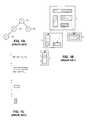
- FIGS. 1A, 1 B and 1 Cillustrate how a layout, T, can be composed of a sub-cell A and a sub-cell B, wherein the sub-cell A further includes a sub-cell C.
- FIG. 1Aillustrates a nodal representation of this hierarchy
- FIG. 1Billustrates a corresponding graphical representation.
- FIG. 1Cpresents a specification of the layout in code form.
- the layout, Tincludes a reference list.
- This reference listincludes a reference to cell A along with an associated transformation, T A , and a reference to cell B along with an associated transformation, T B .
- the layout for cell Aincludes geometrical features associated with cell A along with a reference cell C.
- This reference to cell Cis accompanied by a transformation of cell C with respect to A, T CA .
- the layouts for cell B and cell Cinclude geometrical features associated with cell B and cell C, respectively.
- Representing a layout in a hierarchical formcan cause problems for various operations related to fabrication of a semiconductor chip, because interactions between nodes within the hierarchical representation can cause unintended results. These problems can be remedied by collapsing the hierarchy down into a single monolithic layout before performing the operations. Unfortunately, this can be prohibitively slow because the operations must be applied to the entire monolithic layout, even though many of the cells in the layout may be repeated.
- phase shiftersare often incorporated into a mask in order to achieve line widths that are smaller than the wavelength of the exposure energy that is used to expose the photoresist layer through the mask.
- the destructive interference caused by two adjacent clear areas on a maskis used to create an unexposed area on the photoresist layer. This is accomplished by exploiting the fact that exposure energy passing through a mask's clear regions exhibits a wave characteristic having a phase that is a function of the distance the exposure energy travels through the mask material.
- a phase shifteris composed of a zero degree phase clear area 254 that works in concert with a 180-degree phase clear area 258 to reduce the width of polysilicon line 256 in the gate region of a transistor 250 .
- This first transistorselectively creates a conducting path between diffusion region 252 and diffusion region 260 .
- a thin chromium regulator 255can be added to the mask between zero-degree phase clear area 254 and 180-degree phase clear area 258 in order to better control gate width.
- phase shifteris typically incorporated into a separate phase shifting mask, which is used to reduce the width of polysilicon line 256 in the gate region of transistor 250 .
- Phase shiftersare typically extended past the active diffusion region of a transistor by a certain margin.
- the phase shifter comprised of the zero-degree phase region 204 and 180-degree phase region 206is extended past the endcap of the transistor by an endcap margin 212 (for example, 200 nm).
- the phase shifteris extended past the active diffusion region by a fieldcap margin 214 (for example, 80 nm).
- the endcap margin 212is larger than the fieldcap margin 214 because the transistor endcap may be susceptible to line end shortening, which can be somewhat mitigated by extending the phase shifter by an additional margin.
- Sizing phase shifterscan be a problem in a hierarchical layout because interactions between cells may case endcaps to become fieldcaps.
- endcap 306 in cell 302joins with endcap 316 in cell 304 so that they are no longer endcaps.
- endcap 306 in cell 302interacts with polysilicon region 322 in cell 320 to form a fieldcap.
- thiscan only be accomplished by collapsing the design hierarchy so that the interactions become visible.
- collapsing the design hierarchycan greatly increase the time required to process the layout.
- One embodiment of the inventionprovides a system for analyzing a layout related to a circuit on a semiconductor chip.
- the systemoperates by receiving a design hierarchy specifying the layout of the circuit.
- This layoutincludes a set of hierarchically organized nodes, wherein a given node specifies a geometrical feature that is comprised of lower-level geometrical features that are represented by lower-level nodes located under the given node in the design hierarchy.
- the systemoperates by modifying the design hierarchy by examining a set of sibling nodes that are located under a parent node in the design hierarchy in order to identify a set of interacting geometrical features between the set of sibling nodes. Next, the system then moves the set of interacting geometrical features to a new child node under the parent node, and then performs an analysis on the modified design hierarchy.
- the systemidentifies other sets of sibling nodes with equivalent sets of interacting geometrical features. This allows the system to use the new child node in analyzing the other sets of sibling nodes, so that additional child nodes do not have to be recreated for the other sets of sibling nodes.
- the systemwhile moving the set of interacting geometrical features to the new child node, the system first moves the set of interacting geometrical features from the set of sibling nodes to the parent node. Next, the system creates the new child node under the parent node, and then moves the set of interacting geometrical features from the parent node to the new child node.
- the systemalso identifies a second set of interacting geometrical features between the parent node and the set of sibling nodes. The system then moves this second set of interacting geometrical features from the parent node to the set of sibling nodes.
- performing the analysisinvolves identifying transistors and associated transistor endcaps within the circuit, wherein the set of interacting geometrical features defines at least some of the transistors and associated transistor endcaps.
- the systemgenerates phase shifters to be used in fabricating some of the identified transistors, wherein the layout of a given phase shifter is affected by a location of an associated endcap for the given phase shifter.
- the set of interacting geometrical featuresdefine diffusion regions on the semiconductor chip.
- the layoutcan define either features on the semiconductor chip, or a mask that is used to create features on the semiconductor chip.
- the design hierarchyis specified in GDSII format.
- One embodiment of the inventionprovides a system for analyzing a layout related to a circuit on a semiconductor chip.
- the systemoperates by receiving a design hierarchy specifying the layout of the circuit.
- This design hierarchyincludes a set of hierarchically organized nodes, wherein a given node in the design hierarchy specifies a geometrical feature that is comprised of lower-level geometrical features that are represented by lower-level nodes located under the given node in the design hierarchy.
- the systemmodifies the design hierarchy by, examining a set of sibling nodes that are located under a parent node in the design hierarchy in order to identify a set of interacting geometrical features between the set of sibling nodes.
- the systemthen moves the set of interacting geometrical features from the sibling nodes to the parent node, so that the interaction is visible at the parent node. Note that other geometrical features that do not interact remain at the sibling nodes and are not moved to the parent node.
- the systemthen performs an analysis on the modified design hierarchy. This involves analyzing the set of interacting geometrical features at the parent node.
- the systemdetermines at a parent node whether interactions between related sibling nodes cause transistor endcaps to become fieldcaps, and if so, moves geometrical features that caused the interactions to the parent node.
- the set of interacting geometrical featuresdefine polysilicon regions and diffusion regions on the semiconductor chip.
- FIG. 1Aillustrates a hierarchical representation of a layout in nodal form.
- FIG. 1Billustrates a hierarchical representation of the layout in graphical form.
- FIG. 1Cillustrates a hierarchical representation of the layout in code form.
- FIG. 2Aillustrates a phase shifter used to form a transistor.
- FIG. 2Billustrates endcap and fieldcap margins for a phase shifter.
- FIG. 3Aillustrates an interaction between transistor endcaps in different cells.
- FIG. 3Billustrates an interaction between a transistor endcap and a polysilicon line from different cells.
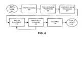
- FIG. 4illustrates the processing of a hierarchical layout in accordance with an embodiment of the invention.
- FIG. 5Apresents a flow chart illustrating the “push diffusion” process in accordance with an embodiment of the invention.
- FIG. 5Billustrates and exemplary hierarchical layout in accordance with an embodiment of the invention.
- FIG. 6presents a flow chart illustrating the processing of a composite gate in accordance with an embodiment of the invention.
- FIG. 7illustrates an exemplary hierarchical layout in accordance with an embodiment of the invention.
- FIG. 8illustrates an additional exemplary hierarchical layout in accordance with an embodiment of the invention.
- FIG. 4illustrates the processing of a hierarchical layout in accordance with an embodiment of the invention.
- the systemstarts with an input layout 402 in a hierarchical format, such as GDSII stream format.
- the systemperforms a preprocessing operation 404 , which modifies cells in input layout 402 in order to improve the efficiency of subsequent processing operations. For example, the system may collapse small cells that contain too few geometrical features (shapes) into other cells. This reduces the inefficiency of having to process too many small cells.
- the systemmay also merge cells that have too many overlapping geometrical features.
- This operationcan move features that specify diffusion regions down to child nodes that have interacting polys with diffusion regions from parent or other sibling nodes, and can thereby create new gates at the child nodes. This process is described in more detail below with reference to FIG. 5 .
- the next processinvolves performing “composite gate” processing 408 to move to the common parent the interacting gates from child nodes. This composite gate processing is described in more detail below with reference to FIG. 6 .
- some embodiments of the present inventionperform only push diffusion processing 406 and not composite gate processing 408 , while other embodiments perform only composite gate processing 408 and not push diffusion processing 406 . Yet other embodiments perform both push diffusion processing 406 and composite gate processing 408 .
- the systemperforms a shifter placement operation 410 to place phase shifters over identified transistors. Note that these phase shifters are sized based upon the existence of endcaps and fieldcaps on the transistors.
- the systemalso performs a design rule checking operation 412 to ensure that the shifter placement does not violate design rules. Note that the system may additionally iterate the shifter placement operation 410 and the design rule checking operation 412 in order to satisfy the design rules.
- the systemalso performs a coloring operation 414 on the phase shifters to ensure that the phase shifters do not violate coloring constraints.
- the coloring operation 414the zero-degree phase regions and the 180-degree phase regions of the shifters are colored with different colors.
- the systemthen checks for unintended interactions between differently colored regions in order to prevent unintended side effects during the phase shifting process.
- the systemAfter the coloring operation 414 , the system produces output layout 416 , which includes phase shifters used to produce the circuit.
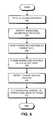
- FIG. 5Apresents a flow chart illustrating the push diffusion process in accordance with an embodiment of the invention.
- the systemstarts by receiving a design hierarchy that specifies the circuit layout (step 502 ).
- the systemperforms the following operations for each parent node and associated child node in the design hierarchy.
- the systemfirst identifies interacting diffusion and poly geometries (step 504 ). These interactions can take place between child (sibling) nodes or between the parent node and the child nodes. For example, in FIG. 5B, the system finds interaction regions between child nodes A and B, as well as interactions between parent node T and child nodes A and B.
- the systemmoves the diffusion geometries within these interacting regions to the parent node T (step 506 ). In one embodiment of the present invention, these interacting features define diffusion regions in the circuit.
- the systemidentifies the child cells that have poly geometries that interact with these diffusion geometries, and creates a new clone copy of child node, A′, (step 508 ) and then moves the interacting geometrical features to the new child node, A′ (step 510 ).
- the processalso identifies identical geometries that are being moved to different instances of the same cell in order to minimize numbers of the clones created for the cell.
- FIG. 6presents a flow chart illustrating the processing of a composite gate in accordance with an embodiment of the invention.
- the systemstarts by receiving a design hierarchy that specifies the circuit layout (step 602 ).
- the systemfirst identifies interacting geometrical features (step 604 ). These interactions can take place between child (sibling) nodes or between the parent node and the child node. For example, in FIG. 7, the system finds interactions between child nodes A 706 and B 707 and between parent node G 703 and child nodes A 706 and B 707 . Next, the system moves the interacting features to the parent node G 703 (step 606 ).
- the systemdoes not redo the analysis, but instead uses the analysis that has already been done for the interacting geometrical features (step 608 ). For example referring to FIG. 8, if the same interacting geometrical features occur under parent node T 802 between sibling nodes A 808 and B 809 , the system does note redo the analysis on the interacting features for nodes A 808 and B 809 , but instead reuses the analysis for nodes A 806 and B 807 .
- the systemdetermines if a set of interacting features are equivalent by determining if they have the same cells interacting with the same relative transformation with respect to each other. In this case, the region of interaction can be duplicated.
- the systemdetects transistors and associated endcaps for node H 704 (step 610 ). This can involve determining at cell T 702 whether an endcap in a cell G 703 interacts with other endcaps or polysilicon features in cell H 704 or in cell I 705 . If any endcaps are changed through interactions with other cells, the system moves the interacting shapes and their associated gates to the parent node T 702 (step 612 ). Note that the other features that are not involved in the interaction remain located at the child nodes G 703 , H 704 and I 705 .
- shifter placement 410can be performed on the modified design hierarchy, wherein diffusion layers are in child nodes and geometries are in parent nodes.
- a computer readable storage mediumwhich may be any device or medium that can store code and/or data for use by a computer system.
- the transmission mediummay include a communications network, such as the Internet.
Landscapes
- Engineering & Computer Science (AREA)
- Computer Hardware Design (AREA)
- Physics & Mathematics (AREA)
- Theoretical Computer Science (AREA)
- Evolutionary Computation (AREA)
- Geometry (AREA)
- General Engineering & Computer Science (AREA)
- General Physics & Mathematics (AREA)
- Design And Manufacture Of Integrated Circuits (AREA)
Abstract
Description
Claims (22)
Priority Applications (1)
| Application Number | Priority Date | Filing Date | Title |
|---|---|---|---|
| US09/953,119US6738958B2 (en) | 2001-09-10 | 2001-09-10 | Modifying a hierarchical representation of a circuit to process composite gates |
Applications Claiming Priority (1)
| Application Number | Priority Date | Filing Date | Title |
|---|---|---|---|
| US09/953,119US6738958B2 (en) | 2001-09-10 | 2001-09-10 | Modifying a hierarchical representation of a circuit to process composite gates |
Publications (2)
| Publication Number | Publication Date |
|---|---|
| US20030051219A1 US20030051219A1 (en) | 2003-03-13 |
| US6738958B2true US6738958B2 (en) | 2004-05-18 |
Family
ID=25493593
Family Applications (1)
| Application Number | Title | Priority Date | Filing Date |
|---|---|---|---|
| US09/953,119Expired - LifetimeUS6738958B2 (en) | 2001-09-10 | 2001-09-10 | Modifying a hierarchical representation of a circuit to process composite gates |
Country Status (1)
| Country | Link |
|---|---|
| US (1) | US6738958B2 (en) |
Cited By (16)
| Publication number | Priority date | Publication date | Assignee | Title |
|---|---|---|---|---|
| US20030135829A1 (en)* | 2002-01-17 | 2003-07-17 | Srinivas Garrepally | Methodology of creating an object database from a Gerber file |
| US20050138591A1 (en)* | 2003-12-19 | 2005-06-23 | Fujitsu Limited | Layout device |
| US20060143589A1 (en)* | 2004-12-23 | 2006-06-29 | Invarium, Inc. | Method and system for reticle-wide hierarchy management for representational and computational reuse in integrated circuit layout design |
| US20080077617A1 (en)* | 2006-09-27 | 2008-03-27 | Rockwell Automation Technologies, Inc. | Universal, hierarchical layout of assets in a facility |
| US20080077512A1 (en)* | 2006-09-27 | 2008-03-27 | Rockwell Automation Technologies, Inc. | Graphical interface for display of assets in an asset management system |
| US20080126377A1 (en)* | 2006-09-27 | 2008-05-29 | Rockwell Automation Technologies, Inc. | Aggregating audit information with field conditions |
| US20090037302A1 (en)* | 2006-09-27 | 2009-02-05 | Rockwell Automation Technologies, Inc. | Programmatically scheduled verification |
| US20100058269A1 (en)* | 2008-08-29 | 2010-03-04 | International Business Machines Corporation | Uniquification and Parent-Child Constructs for 1xN VLSI Design |
| US20100058260A1 (en)* | 2008-08-29 | 2010-03-04 | International Business Machines Corporation | Integrated Design for Manufacturing for 1xN VLSI Design |
| US20100058275A1 (en)* | 2008-08-29 | 2010-03-04 | International Business Machines Corporation | Top Level Hierarchy Wiring Via 1xN Compiler |
| US20100107130A1 (en)* | 2008-10-23 | 2010-04-29 | International Business Machines Corporation | 1xn block builder for 1xn vlsi design |
| US8122399B2 (en) | 2008-08-28 | 2012-02-21 | International Business Machines Corporation | Compiler for closed-loop 1×N VLSI design |
| US8132134B2 (en) | 2008-08-28 | 2012-03-06 | International Business Machines Corporation | Closed-loop 1×N VLSI design system |
| US8136062B2 (en) | 2008-08-28 | 2012-03-13 | International Business Machines Corporation | Hierarchy reassembler for 1×N VLSI design |
| US8829610B2 (en) | 2012-05-15 | 2014-09-09 | United Microelectronics Corp. | Method for forming semiconductor layout patterns, semiconductor layout patterns, and semiconductor structure |
| US10379446B2 (en) | 2015-09-28 | 2019-08-13 | Asml Netherlands B.V. | Lithography system, method and computer program product for hierarchical representation of two-dimensional or three-dimensional shapes |
Families Citing this family (1)
| Publication number | Priority date | Publication date | Assignee | Title |
|---|---|---|---|---|
| US6735752B2 (en)* | 2001-09-10 | 2004-05-11 | Numerical Technologies, Inc. | Modifying a hierarchical representation of a circuit to process features created by interactions between cells |
Citations (94)
| Publication number | Priority date | Publication date | Assignee | Title |
|---|---|---|---|---|
| US4037918A (en) | 1974-08-03 | 1977-07-26 | Matsushita Electric Industrial Co., Ltd. | Fourier-transform holography by pseudo-random phase shifting |
| US4456371A (en) | 1982-06-30 | 1984-06-26 | International Business Machines Corporation | Optical projection printing threshold leveling arrangement |
| JPS6267547A (en) | 1985-09-20 | 1987-03-27 | Hitachi Ltd | photomask |
| JPH02140743A (en) | 1988-11-22 | 1990-05-30 | Hitachi Ltd | Method of manufacturing integrated circuit device |
| JPH0380525A (en) | 1989-04-04 | 1991-04-05 | Matsushita Electric Ind Co Ltd | Proximity effect correction method |
| EP0464492A1 (en) | 1990-06-21 | 1992-01-08 | Matsushita Electronics Corporation | A photomask used by photolithography and a process of producing the same |
| US5182718A (en) | 1989-04-04 | 1993-01-26 | Matsushita Electric Industrial Co., Ltd. | Method and apparatus for writing a pattern on a semiconductor sample based on a resist pattern corrected for proximity effects resulting from direct exposure of the sample by a charged-particle beam or light |
| JPH0667403A (en) | 1992-03-27 | 1994-03-11 | Nippon Telegr & Teleph Corp <Ntt> | Photomask and method for processing mask pattern data |
| US5302477A (en) | 1992-08-21 | 1994-04-12 | Intel Corporation | Inverted phase-shifted reticle |
| US5308741A (en) | 1992-07-31 | 1994-05-03 | Motorola, Inc. | Lithographic method using double exposure techniques, mask position shifting and light phase shifting |
| US5316878A (en) | 1991-06-19 | 1994-05-31 | Oki Electric Industry Co., Ltd. | Pattern forming method and photomasks used therefor |
| US5324600A (en) | 1991-07-12 | 1994-06-28 | Oki Electric Industry Co., Ltd. | Method of forming resist pattern and photomask therefor |
| US5328807A (en) | 1990-06-11 | 1994-07-12 | Hitichi, Ltd. | Method of forming a pattern |
| US5334542A (en) | 1991-11-27 | 1994-08-02 | Oki Electric Industry Co., Ltd. | Method of forming T-shaped electrode |
| US5364716A (en) | 1991-09-27 | 1994-11-15 | Fujitsu Limited | Pattern exposing method using phase shift and mask used therefor |
| JPH07111528A (en) | 1993-10-12 | 1995-04-25 | Matsushita Electric Ind Co Ltd | Answering machine |
| EP0653679A2 (en) | 1989-04-28 | 1995-05-17 | Fujitsu Limited | Mask, mask producing method and pattern forming method using mask |
| US5424154A (en) | 1993-12-10 | 1995-06-13 | Intel Corporation | Lithographic emhancement method and apparatus for randomly spaced structures |
| US5432714A (en) | 1993-01-29 | 1995-07-11 | International Business Machines Corporation | System and method for preparing shape data for proximity correction |
| US5472814A (en) | 1994-11-17 | 1995-12-05 | International Business Machines Corporation | Orthogonally separated phase shifted and unphase shifted mask patterns for image improvement |
| US5480746A (en) | 1991-10-01 | 1996-01-02 | Oki Electric Industry Co., Ltd. | Photomask and method of forming resist pattern using the same |
| JPH0851068A (en) | 1995-05-10 | 1996-02-20 | Hitachi Ltd | Mask formation method |
| EP0698821A1 (en) | 1994-08-03 | 1996-02-28 | International Business Machines Corporation | High resolution phase edge lithography without the need for a trim mask |
| US5496666A (en) | 1994-10-27 | 1996-03-05 | Chartered Semiconductor Manufacturing Pte Ltd. | Contact hole mask for semiconductor fabrication |
| US5503951A (en) | 1994-02-14 | 1996-04-02 | International Business Machines Corp. | Attenuating phase-shift mask structure and fabrication method |
| US5523186A (en) | 1994-12-16 | 1996-06-04 | International Business Machines Corporation | Split and cover technique for phase shifting photolithography |
| DE19545163A1 (en) | 1994-12-02 | 1996-06-05 | Hyundai Electronics Ind | Phase shift mask for the formation of contact holes with micro dimensions |
| US5527645A (en) | 1993-04-21 | 1996-06-18 | Pati; Yagyensh C. | Systematic method for production of phase-shifting photolithographic masks |
| US5532090A (en) | 1995-03-01 | 1996-07-02 | Intel Corporation | Method and apparatus for enhanced contact and via lithography |
| US5533148A (en) | 1993-09-30 | 1996-07-02 | International Business Machines Corporation | Method for restructuring physical design images into hierarchical data models |
| US5537648A (en) | 1994-08-15 | 1996-07-16 | International Business Machines Corporation | Geometric autogeneration of "hard" phase-shift designs for VLSI |
| US5538815A (en) | 1992-09-14 | 1996-07-23 | Kabushiki Kaisha Toshiba | Method for designing phase-shifting masks with automatization capability |
| US5539568A (en) | 1994-06-16 | 1996-07-23 | Texas Instruments Incorporated | Method of exposing a light sensitive material |
| US5565286A (en) | 1994-11-17 | 1996-10-15 | International Business Machines Corporation | Combined attenuated-alternating phase shifting mask structure and fabrication methods therefor |
| US5573890A (en) | 1994-07-18 | 1996-11-12 | Advanced Micro Devices, Inc. | Method of optical lithography using phase shift masking |
| US5595843A (en) | 1995-03-30 | 1997-01-21 | Intel Corporation | Layout methodology, mask set, and patterning method for phase-shifting lithography |
| US5631110A (en) | 1994-07-05 | 1997-05-20 | Nec Corporation | Process of fabricating photo-mask used for modified illumination, projection aligner using the photo-mask and method of transferring pattern image from the photo-mask to photo-sensitive layer |
| US5657235A (en) | 1995-05-03 | 1997-08-12 | International Business Machines Corporation | Continuous scale optical proximity correction by mask maker dose modulation |
| JP2650962B2 (en) | 1988-05-11 | 1997-09-10 | 株式会社日立製作所 | Exposure method, element forming method, and semiconductor element manufacturing method |
| US5682323A (en) | 1995-03-06 | 1997-10-28 | Lsi Logic Corporation | System and method for performing optical proximity correction on macrocell libraries |
| US5725969A (en) | 1995-09-25 | 1998-03-10 | Lg Semicon Co., Ltd. | Method of manufacturing phase-shifting mask comprising a light shield pattern on a phase-shifting attenuatting layer |
| WO1998012605A1 (en) | 1996-09-18 | 1998-03-26 | Numerical Technologies, Inc. | Phase shifting circuit manufacture method and apparatus |
| US5761075A (en) | 1993-12-28 | 1998-06-02 | Kabushiki Kaisha Toshiba | Apparatus for designing photomasks |
| US5807649A (en) | 1996-10-31 | 1998-09-15 | International Business Machines Corporation | Lithographic patterning method and mask set therefor with light field trim mask |
| US5815685A (en) | 1994-09-16 | 1998-09-29 | Mitsubishi Denki Kabushiki Kaisha | Apparatus and method for correcting light proximity effects by predicting mask performance |
| US5827623A (en) | 1995-10-31 | 1998-10-27 | Nec Corporation | Optical proximity correction halftone type phase shift photomask |
| US5847959A (en) | 1997-01-28 | 1998-12-08 | Etec Systems, Inc. | Method and apparatus for run-time correction of proximity effects in pattern generation |
| US5858580A (en) | 1997-09-17 | 1999-01-12 | Numerical Technologies, Inc. | Phase shifting circuit manufacture method and apparatus |
| US5885734A (en) | 1996-08-15 | 1999-03-23 | Micron Technology, Inc. | Process for modifying a hierarchical mask layout |
| WO1999014636A1 (en) | 1997-09-17 | 1999-03-25 | Numerical Technologies, Inc. | Method and apparatus for data hierarchy maintenance in a system for mask description |
| WO1999014638A1 (en) | 1997-09-17 | 1999-03-25 | Numerical Technologies, Inc. | Design rule checking system and method |
| US5923566A (en) | 1997-03-25 | 1999-07-13 | International Business Machines Corporation | Phase shifted design verification routine |
| US5923562A (en) | 1996-10-18 | 1999-07-13 | International Business Machines Corporation | Method for automatically eliminating three way intersection design conflicts in phase edge, phase shift designs |
| GB2333613A (en) | 1998-01-23 | 1999-07-28 | Sony Corp | Mask pattern generating method |
| US5994002A (en) | 1996-09-06 | 1999-11-30 | Matsushita Electric Industrial Co., Ltd. | Photo mask and pattern forming method |
| US5998068A (en) | 1997-01-28 | 1999-12-07 | Matsushita Electric Industrial Co., Ltd. | Reticle and pattern formation method |
| US6004702A (en) | 1997-11-28 | 1999-12-21 | United Microelectronics Corp. | Phase-shifting mask structure and method of fabricating the same |
| US6009250A (en) | 1997-09-30 | 1999-12-28 | Synopsys, Inc. | Selective flattening in layout areas in computer implemented integrated circuit design |
| US6009251A (en) | 1997-09-30 | 1999-12-28 | Synopsys, Inc. | Method and system for layout verification of an integrated circuit design with reusable subdesigns |
| US6011911A (en) | 1997-09-30 | 2000-01-04 | Synopsys, Inc. | Layout overlap detection with selective flattening in computer implemented integrated circuit design |
| US6010807A (en) | 1997-11-22 | 2000-01-04 | United Microelectronics Corp. | Phase-shifting mask for photolithography in semiconductor fabrications |
| US6057063A (en) | 1997-04-14 | 2000-05-02 | International Business Machines Corporation | Phase shifted mask design system, phase shifted mask and VLSI circuit devices manufactured therewith |
| US6064806A (en) | 1997-10-03 | 2000-05-16 | Mentor Graphics Corporation | System and method for converting a polygon-based layout of an integrated circuit design to an object-based layout |
| US6066180A (en) | 1997-03-04 | 2000-05-23 | International Business Machines Corporation | Automatic generation of phase shift masks using net coloring |
| US6077630A (en) | 1998-01-08 | 2000-06-20 | Micron Technology, Inc. | Subresolution grating for attenuated phase shifting mask fabrication |
| US6077310A (en) | 1995-12-22 | 2000-06-20 | Kabushiki Kaisha Toshiba | Optical proximity correction system |
| US6081658A (en) | 1997-12-31 | 2000-06-27 | Avant! Corporation | Proximity correction system for wafer lithography |
| US6083275A (en) | 1998-01-09 | 2000-07-04 | International Business Machines Corporation | Optimized phase shift design migration |
| US6130012A (en) | 1999-01-13 | 2000-10-10 | Advanced Micro Devices, Inc. | Ion beam milling to generate custom reticles |
| US6139994A (en) | 1999-06-25 | 2000-10-31 | Broeke; Doug Van Den | Use of intersecting subresolution features for microlithography |
| US6185727B1 (en) | 1995-12-12 | 2001-02-06 | International Business Machines Corporation | Design verification for asymmetric phase shift mask layouts |
| WO2001023961A1 (en) | 1999-09-28 | 2001-04-05 | Mentor Graphics Corporation | Method and apparatus for determining phase shifts and trim masks for an integrated circuit |
| US20010000240A1 (en) | 1996-09-18 | 2001-04-12 | Yao-Ting Wang | Phase shifting circuit manufacture method and apparatus |
| US6251549B1 (en) | 1999-07-19 | 2001-06-26 | Marc David Levenson | Generic phase shift mask |
| WO2002003140A1 (en) | 2000-07-05 | 2002-01-10 | Numerical Technologies, Inc. | Phase shift masking for complex patterns |
| US6338922B1 (en) | 2000-05-08 | 2002-01-15 | International Business Machines Corporation | Optimized alternating phase shifted mask design |
| US6339836B1 (en) | 1998-08-24 | 2002-01-15 | Mentor Graphics Corporation | Automated design partitioning |
| US20020010904A1 (en) | 2000-07-24 | 2002-01-24 | Ayres Ronald Frederick | Reduced disk access for complex mask generation |
| US6370679B1 (en) | 1997-09-17 | 2002-04-09 | Numerical Technologies, Inc. | Data hierarchy layout correction and verification method and apparatus |
| WO2002029491A1 (en) | 2000-09-29 | 2002-04-11 | Numerical Technologies, Inc. | Method for high yield reticle formation |
| US20020083410A1 (en) | 2000-10-25 | 2002-06-27 | Numerical Technologies, Inc. | Resolving phase-shift conflicts in layouts using weighted links between phase shifters |
| US20020122994A1 (en) | 2000-07-05 | 2002-09-05 | Cote Michel Luc | Design and layout of phase shifting photolithographic masks |
| US20020129327A1 (en) | 2000-07-05 | 2002-09-12 | Numerical Technologies, Inc. | Phase shifting design and layout for static random access memory |
| US20020127479A1 (en) | 2000-07-05 | 2002-09-12 | Christophe Pierrat | Phase shift masking for complex patterns with proximity adjustments |
| US6453452B1 (en) | 1997-12-12 | 2002-09-17 | Numerical Technologies, Inc. | Method and apparatus for data hierarchy maintenance in a system for mask description |
| WO2002073312A1 (en) | 2001-03-08 | 2002-09-19 | Numerical Technologies, Inc. | Alternating phase shift masking for multiple levels of masking resolution |
| US20020136964A1 (en) | 2001-03-23 | 2002-09-26 | Numerical Technologies | Blank for alternating PSM photomask with charge dissipation layer |
| US20020142231A1 (en) | 2001-04-03 | 2002-10-03 | Numerical Technologies, Inc. | Method and apparatus for reducing incidental exposure by using a phase shifter with a variable regulator |
| US20020142232A1 (en) | 2001-04-03 | 2002-10-03 | Numerical Technologies, Inc. | Using double exposure effects during phase shifting to control line end shortening |
| US20020144232A1 (en) | 2001-04-03 | 2002-10-03 | Numerical Technologies, Inc. | Alleviating line end shortening in transistor endcaps by extending phase shifters |
| US20020152454A1 (en) | 2000-07-05 | 2002-10-17 | Numerical Technologies, Inc. | Design data format and hierarchy management for processing |
| US20020152449A1 (en) | 2001-04-13 | 2002-10-17 | Chin-Hsen Lin | Generating an instance-based representation of a design hierarchy |
| US20020155363A1 (en) | 2000-07-05 | 2002-10-24 | Numerical Technologies, Inc. | Standard cell design incorporating phase information |
| US6560766B2 (en)* | 2001-07-26 | 2003-05-06 | Numerical Technologies, Inc. | Method and apparatus for analyzing a layout using an instance-based representation |
- 2001
- 2001-09-10USUS09/953,119patent/US6738958B2/ennot_activeExpired - Lifetime
Patent Citations (111)
| Publication number | Priority date | Publication date | Assignee | Title |
|---|---|---|---|---|
| US4037918A (en) | 1974-08-03 | 1977-07-26 | Matsushita Electric Industrial Co., Ltd. | Fourier-transform holography by pseudo-random phase shifting |
| US4456371A (en) | 1982-06-30 | 1984-06-26 | International Business Machines Corporation | Optical projection printing threshold leveling arrangement |
| JPS6267547A (en) | 1985-09-20 | 1987-03-27 | Hitachi Ltd | photomask |
| JP2650962B2 (en) | 1988-05-11 | 1997-09-10 | 株式会社日立製作所 | Exposure method, element forming method, and semiconductor element manufacturing method |
| US5352550A (en) | 1988-11-22 | 1994-10-04 | Hitachi, Ltd. | Mask for manufacturing semiconductor devices and method of manufacture thereof |
| JPH02140743A (en) | 1988-11-22 | 1990-05-30 | Hitachi Ltd | Method of manufacturing integrated circuit device |
| JPH0380525A (en) | 1989-04-04 | 1991-04-05 | Matsushita Electric Ind Co Ltd | Proximity effect correction method |
| US5182718A (en) | 1989-04-04 | 1993-01-26 | Matsushita Electric Industrial Co., Ltd. | Method and apparatus for writing a pattern on a semiconductor sample based on a resist pattern corrected for proximity effects resulting from direct exposure of the sample by a charged-particle beam or light |
| EP0653679A2 (en) | 1989-04-28 | 1995-05-17 | Fujitsu Limited | Mask, mask producing method and pattern forming method using mask |
| US5328807A (en) | 1990-06-11 | 1994-07-12 | Hitichi, Ltd. | Method of forming a pattern |
| EP0464492A1 (en) | 1990-06-21 | 1992-01-08 | Matsushita Electronics Corporation | A photomask used by photolithography and a process of producing the same |
| US5316878A (en) | 1991-06-19 | 1994-05-31 | Oki Electric Industry Co., Ltd. | Pattern forming method and photomasks used therefor |
| US5324600A (en) | 1991-07-12 | 1994-06-28 | Oki Electric Industry Co., Ltd. | Method of forming resist pattern and photomask therefor |
| US5364716A (en) | 1991-09-27 | 1994-11-15 | Fujitsu Limited | Pattern exposing method using phase shift and mask used therefor |
| US5480746A (en) | 1991-10-01 | 1996-01-02 | Oki Electric Industry Co., Ltd. | Photomask and method of forming resist pattern using the same |
| US5334542A (en) | 1991-11-27 | 1994-08-02 | Oki Electric Industry Co., Ltd. | Method of forming T-shaped electrode |
| JPH0667403A (en) | 1992-03-27 | 1994-03-11 | Nippon Telegr & Teleph Corp <Ntt> | Photomask and method for processing mask pattern data |
| US5308741A (en) | 1992-07-31 | 1994-05-03 | Motorola, Inc. | Lithographic method using double exposure techniques, mask position shifting and light phase shifting |
| US5302477A (en) | 1992-08-21 | 1994-04-12 | Intel Corporation | Inverted phase-shifted reticle |
| US5538815A (en) | 1992-09-14 | 1996-07-23 | Kabushiki Kaisha Toshiba | Method for designing phase-shifting masks with automatization capability |
| US5432714A (en) | 1993-01-29 | 1995-07-11 | International Business Machines Corporation | System and method for preparing shape data for proximity correction |
| US5527645A (en) | 1993-04-21 | 1996-06-18 | Pati; Yagyensh C. | Systematic method for production of phase-shifting photolithographic masks |
| US5533148A (en) | 1993-09-30 | 1996-07-02 | International Business Machines Corporation | Method for restructuring physical design images into hierarchical data models |
| JPH07111528A (en) | 1993-10-12 | 1995-04-25 | Matsushita Electric Ind Co Ltd | Answering machine |
| US5424154A (en) | 1993-12-10 | 1995-06-13 | Intel Corporation | Lithographic emhancement method and apparatus for randomly spaced structures |
| US5498579A (en) | 1993-12-10 | 1996-03-12 | Intel Corporation | Method of producing semiconductor device layer layout |
| US5761075A (en) | 1993-12-28 | 1998-06-02 | Kabushiki Kaisha Toshiba | Apparatus for designing photomasks |
| US5503951A (en) | 1994-02-14 | 1996-04-02 | International Business Machines Corp. | Attenuating phase-shift mask structure and fabrication method |
| US5539568A (en) | 1994-06-16 | 1996-07-23 | Texas Instruments Incorporated | Method of exposing a light sensitive material |
| US5631110A (en) | 1994-07-05 | 1997-05-20 | Nec Corporation | Process of fabricating photo-mask used for modified illumination, projection aligner using the photo-mask and method of transferring pattern image from the photo-mask to photo-sensitive layer |
| US5702848A (en) | 1994-07-18 | 1997-12-30 | Advanced Micro Devices, Inc. | Mask for optical lithography using phase shift masking and integrated circuit produced therefrom |
| US5766804A (en) | 1994-07-18 | 1998-06-16 | Advanced Micro Devices, Inc. | Method of optical lithography using phase shift masking |
| US5573890A (en) | 1994-07-18 | 1996-11-12 | Advanced Micro Devices, Inc. | Method of optical lithography using phase shift masking |
| US5766806A (en) | 1994-07-18 | 1998-06-16 | Advanced Micro Devices, Inc. | Method of optical lithography using phase shift masking |
| EP0698821A1 (en) | 1994-08-03 | 1996-02-28 | International Business Machines Corporation | High resolution phase edge lithography without the need for a trim mask |
| US5537648A (en) | 1994-08-15 | 1996-07-16 | International Business Machines Corporation | Geometric autogeneration of "hard" phase-shift designs for VLSI |
| US5636131A (en) | 1994-08-15 | 1997-06-03 | International Business Machines Corporation | Geometric autogeneration of"hard"phase-shift designs for VLSI |
| US5815685A (en) | 1994-09-16 | 1998-09-29 | Mitsubishi Denki Kabushiki Kaisha | Apparatus and method for correcting light proximity effects by predicting mask performance |
| US5496666A (en) | 1994-10-27 | 1996-03-05 | Chartered Semiconductor Manufacturing Pte Ltd. | Contact hole mask for semiconductor fabrication |
| US5565286A (en) | 1994-11-17 | 1996-10-15 | International Business Machines Corporation | Combined attenuated-alternating phase shifting mask structure and fabrication methods therefor |
| US5472814A (en) | 1994-11-17 | 1995-12-05 | International Business Machines Corporation | Orthogonally separated phase shifted and unphase shifted mask patterns for image improvement |
| DE19545163A1 (en) | 1994-12-02 | 1996-06-05 | Hyundai Electronics Ind | Phase shift mask for the formation of contact holes with micro dimensions |
| US5523186A (en) | 1994-12-16 | 1996-06-04 | International Business Machines Corporation | Split and cover technique for phase shifting photolithography |
| US5532090A (en) | 1995-03-01 | 1996-07-02 | Intel Corporation | Method and apparatus for enhanced contact and via lithography |
| US5682323A (en) | 1995-03-06 | 1997-10-28 | Lsi Logic Corporation | System and method for performing optical proximity correction on macrocell libraries |
| US5635316A (en) | 1995-03-30 | 1997-06-03 | Intel Corporation | Layout methodology, mask set, and patterning method for phase-shifting lithography |
| US5620816A (en) | 1995-03-30 | 1997-04-15 | Intel Corporation | Layout methodology, mask set, and patterning method for phase-shifting lithography |
| US5595843A (en) | 1995-03-30 | 1997-01-21 | Intel Corporation | Layout methodology, mask set, and patterning method for phase-shifting lithography |
| US5657235A (en) | 1995-05-03 | 1997-08-12 | International Business Machines Corporation | Continuous scale optical proximity correction by mask maker dose modulation |
| JP2638561B2 (en) | 1995-05-10 | 1997-08-06 | 株式会社日立製作所 | Mask formation method |
| JPH0851068A (en) | 1995-05-10 | 1996-02-20 | Hitachi Ltd | Mask formation method |
| US5725969A (en) | 1995-09-25 | 1998-03-10 | Lg Semicon Co., Ltd. | Method of manufacturing phase-shifting mask comprising a light shield pattern on a phase-shifting attenuatting layer |
| US5827623A (en) | 1995-10-31 | 1998-10-27 | Nec Corporation | Optical proximity correction halftone type phase shift photomask |
| US6185727B1 (en) | 1995-12-12 | 2001-02-06 | International Business Machines Corporation | Design verification for asymmetric phase shift mask layouts |
| US6077310A (en) | 1995-12-22 | 2000-06-20 | Kabushiki Kaisha Toshiba | Optical proximity correction system |
| US5885734A (en) | 1996-08-15 | 1999-03-23 | Micron Technology, Inc. | Process for modifying a hierarchical mask layout |
| US5994002A (en) | 1996-09-06 | 1999-11-30 | Matsushita Electric Industrial Co., Ltd. | Photo mask and pattern forming method |
| US6436590B2 (en) | 1996-09-18 | 2002-08-20 | Numerical Technologies, Inc. | Phase shifting circuit manufacture method and apparatus |
| US20010000240A1 (en) | 1996-09-18 | 2001-04-12 | Yao-Ting Wang | Phase shifting circuit manufacture method and apparatus |
| WO1998012605A1 (en) | 1996-09-18 | 1998-03-26 | Numerical Technologies, Inc. | Phase shifting circuit manufacture method and apparatus |
| US6228539B1 (en) | 1996-09-18 | 2001-05-08 | Numerical Technologies, Inc. | Phase shifting circuit manufacture method and apparatus |
| US20010028985A1 (en) | 1996-09-18 | 2001-10-11 | Yao-Ting Wang | Phase shifting circuit manufacture method and apparatus |
| US6258493B1 (en) | 1996-09-18 | 2001-07-10 | Numerical Technologies, Inc. | Phase shifting circuit manufacture method and apparatus |
| US6420074B2 (en) | 1996-09-18 | 2002-07-16 | Numerial Technologies, Inc. | Phase shifting circuit manufacture method and apparatus |
| US5923562A (en) | 1996-10-18 | 1999-07-13 | International Business Machines Corporation | Method for automatically eliminating three way intersection design conflicts in phase edge, phase shift designs |
| US5807649A (en) | 1996-10-31 | 1998-09-15 | International Business Machines Corporation | Lithographic patterning method and mask set therefor with light field trim mask |
| US5847959A (en) | 1997-01-28 | 1998-12-08 | Etec Systems, Inc. | Method and apparatus for run-time correction of proximity effects in pattern generation |
| US5998068A (en) | 1997-01-28 | 1999-12-07 | Matsushita Electric Industrial Co., Ltd. | Reticle and pattern formation method |
| US6066180A (en) | 1997-03-04 | 2000-05-23 | International Business Machines Corporation | Automatic generation of phase shift masks using net coloring |
| US5923566A (en) | 1997-03-25 | 1999-07-13 | International Business Machines Corporation | Phase shifted design verification routine |
| US6057063A (en) | 1997-04-14 | 2000-05-02 | International Business Machines Corporation | Phase shifted mask design system, phase shifted mask and VLSI circuit devices manufactured therewith |
| US5858580A (en) | 1997-09-17 | 1999-01-12 | Numerical Technologies, Inc. | Phase shifting circuit manufacture method and apparatus |
| US6370679B1 (en) | 1997-09-17 | 2002-04-09 | Numerical Technologies, Inc. | Data hierarchy layout correction and verification method and apparatus |
| WO1999014638A1 (en) | 1997-09-17 | 1999-03-25 | Numerical Technologies, Inc. | Design rule checking system and method |
| WO1999014636A1 (en) | 1997-09-17 | 1999-03-25 | Numerical Technologies, Inc. | Method and apparatus for data hierarchy maintenance in a system for mask description |
| WO1999014637A1 (en) | 1997-09-17 | 1999-03-25 | Numerical Technologies, Inc. | Data hierarchy layout correction and verification method and apparatus |
| US6011911A (en) | 1997-09-30 | 2000-01-04 | Synopsys, Inc. | Layout overlap detection with selective flattening in computer implemented integrated circuit design |
| US6009251A (en) | 1997-09-30 | 1999-12-28 | Synopsys, Inc. | Method and system for layout verification of an integrated circuit design with reusable subdesigns |
| US6009250A (en) | 1997-09-30 | 1999-12-28 | Synopsys, Inc. | Selective flattening in layout areas in computer implemented integrated circuit design |
| US6064806A (en) | 1997-10-03 | 2000-05-16 | Mentor Graphics Corporation | System and method for converting a polygon-based layout of an integrated circuit design to an object-based layout |
| US6010807A (en) | 1997-11-22 | 2000-01-04 | United Microelectronics Corp. | Phase-shifting mask for photolithography in semiconductor fabrications |
| US6004702A (en) | 1997-11-28 | 1999-12-21 | United Microelectronics Corp. | Phase-shifting mask structure and method of fabricating the same |
| US6453452B1 (en) | 1997-12-12 | 2002-09-17 | Numerical Technologies, Inc. | Method and apparatus for data hierarchy maintenance in a system for mask description |
| US6081658A (en) | 1997-12-31 | 2000-06-27 | Avant! Corporation | Proximity correction system for wafer lithography |
| US6077630A (en) | 1998-01-08 | 2000-06-20 | Micron Technology, Inc. | Subresolution grating for attenuated phase shifting mask fabrication |
| US6083275A (en) | 1998-01-09 | 2000-07-04 | International Business Machines Corporation | Optimized phase shift design migration |
| GB2333613A (en) | 1998-01-23 | 1999-07-28 | Sony Corp | Mask pattern generating method |
| US6339836B1 (en) | 1998-08-24 | 2002-01-15 | Mentor Graphics Corporation | Automated design partitioning |
| US6130012A (en) | 1999-01-13 | 2000-10-10 | Advanced Micro Devices, Inc. | Ion beam milling to generate custom reticles |
| US6139994A (en) | 1999-06-25 | 2000-10-31 | Broeke; Doug Van Den | Use of intersecting subresolution features for microlithography |
| US6251549B1 (en) | 1999-07-19 | 2001-06-26 | Marc David Levenson | Generic phase shift mask |
| US6335128B1 (en) | 1999-09-28 | 2002-01-01 | Nicolas Bailey Cobb | Method and apparatus for determining phase shifts and trim masks for an integrated circuit |
| WO2001023961A1 (en) | 1999-09-28 | 2001-04-05 | Mentor Graphics Corporation | Method and apparatus for determining phase shifts and trim masks for an integrated circuit |
| US6338922B1 (en) | 2000-05-08 | 2002-01-15 | International Business Machines Corporation | Optimized alternating phase shifted mask design |
| US20020152454A1 (en) | 2000-07-05 | 2002-10-17 | Numerical Technologies, Inc. | Design data format and hierarchy management for processing |
| US20020122994A1 (en) | 2000-07-05 | 2002-09-05 | Cote Michel Luc | Design and layout of phase shifting photolithographic masks |
| US20020129327A1 (en) | 2000-07-05 | 2002-09-12 | Numerical Technologies, Inc. | Phase shifting design and layout for static random access memory |
| US20020127479A1 (en) | 2000-07-05 | 2002-09-12 | Christophe Pierrat | Phase shift masking for complex patterns with proximity adjustments |
| WO2002003140A1 (en) | 2000-07-05 | 2002-01-10 | Numerical Technologies, Inc. | Phase shift masking for complex patterns |
| US20020155363A1 (en) | 2000-07-05 | 2002-10-24 | Numerical Technologies, Inc. | Standard cell design incorporating phase information |
| US20020010904A1 (en) | 2000-07-24 | 2002-01-24 | Ayres Ronald Frederick | Reduced disk access for complex mask generation |
| WO2002029491A1 (en) | 2000-09-29 | 2002-04-11 | Numerical Technologies, Inc. | Method for high yield reticle formation |
| US20020083410A1 (en) | 2000-10-25 | 2002-06-27 | Numerical Technologies, Inc. | Resolving phase-shift conflicts in layouts using weighted links between phase shifters |
| WO2002073312A1 (en) | 2001-03-08 | 2002-09-19 | Numerical Technologies, Inc. | Alternating phase shift masking for multiple levels of masking resolution |
| US20020136964A1 (en) | 2001-03-23 | 2002-09-26 | Numerical Technologies | Blank for alternating PSM photomask with charge dissipation layer |
| US20020142231A1 (en) | 2001-04-03 | 2002-10-03 | Numerical Technologies, Inc. | Method and apparatus for reducing incidental exposure by using a phase shifter with a variable regulator |
| US20020144232A1 (en) | 2001-04-03 | 2002-10-03 | Numerical Technologies, Inc. | Alleviating line end shortening in transistor endcaps by extending phase shifters |
| US20020142232A1 (en) | 2001-04-03 | 2002-10-03 | Numerical Technologies, Inc. | Using double exposure effects during phase shifting to control line end shortening |
| US20020152449A1 (en) | 2001-04-13 | 2002-10-17 | Chin-Hsen Lin | Generating an instance-based representation of a design hierarchy |
| US6505327B2 (en)* | 2001-04-13 | 2003-01-07 | Numerical Technologies, Inc. | Generating an instance-based representation of a design hierarchy |
| US6560766B2 (en)* | 2001-07-26 | 2003-05-06 | Numerical Technologies, Inc. | Method and apparatus for analyzing a layout using an instance-based representation |
Non-Patent Citations (133)
| Title |
|---|
| Ackmann, P., et al., "Phase Shifting and Optical Proximity Corrections to Improve CD Control on Logic Devices in Manufacturing for Sub 0.35 um I-Line", Advance Micro Devices (8 pages), No date. |
| Asai, S., et al., "High Performance Optical Lithography Using a Separated Light Source", J. Vac. Sci. Technol. B, vol. 10, No. 6, pp. 3023-3026, Nov./Dec. 1992. |
| Barouch, E., et al., "OPTIMASK: An OPC Algorithm for Chrome and Phase-Shift Mask Design", SPIE, Vo. 2440, pp. 192-206, Feb. 1995. |
| Brunner, T., "Rim Phase-Shift Mask Combined with Off-Axis Illumination: A Path to 0.5(lampda) / Numerical Aperture Geometries", Optical Engineering, vol. 32, No. 10, pp. 2337-2343, Oct. 1993. |
| Brunner, T., et al., "170nm Gates Fabricated by Phase-Shift Mask and Top Anti-Reflector Process", SPIE, Optical/Laser Microlithography VI, Vo. 1927, pp. 182-189 (1993). |
| Buraschi, M., et al., "Optical-Diffraction-Based Modulation of Photoresist Profile on Microlithography Applications", Optical Engineering, vol. 28, No. 6, pp. 654-658, Jun. 1989. |
| Burggraaf, P., "Four More Significant Japanese Advances in Phase Shifting Technology", Semiconductor International, p. 16, Dec. 1991. |
| Burggraaf, P., "Lithography's Leading Edge, Part 1: Phase-Shift Technology and Part 2: I-Line and Beyond", Semiconductor International, pp. 43-47 and 52-56, Feb. 1992. |
| Cooke, M., "OPC/PSM Designs For Poly Gate Layers", European Semiconductor, vol. 22, No. 7, pp. 57-59, Jul. 2000. |
| Cote, M., et al., "A Practical Application of Full-Feature Alternating Phase-Shifting Technology for a Phase-Aware Standard-Cell Design Flow", Numerical Technologies Inc. (6 pages), No date. |
| Erdmann, A., "Topography Effects and Wave Aberrations in Advanced PSM-Technology", Fraunhofer Institute of Integrated Circuits (11 pages), No date. |
| Ferguson, R., et al., "Pattern-Dependent Correction of Mask Topography Effects for Alternating Phase-Shifting Masks", IBM Microelectronics, University of California Berkeley (12 pages), No date. |
| Fritze, M., et al., "100-nm Node Lithography with KrF?", MIT Lincoln Lab, Numberical Technologies, Photronics, Arch Chemicals (14 pages), No date. |
| Fukuda, H., "Node-Connection/Quantum Phase-Shifting Mask: Path to Below 0.3um Pitch, Proximity Effect Free, Random Interconnects and Memory Patterning", J. Vac. Sci. Technol. B, vol. 17, No. 6, pp. 3291-3295, Nov./Dec. 1999. |
| Fukuda, H., et al., "Determination of High-Order Lens Aberration Using Phase/Amplitude Linear Algebra", J. Vac. Sci. Technol. B, vol. 17, No. 6, pp. 3318-3321, Nov./Dec. 1999. |
| Fukuda, H., et al., "Patterning of Random Interconnect Using Double Exposure of Strong-Type PSMs", Hitachi Central Research Lab (8 pages), No date. |
| Galan, G., et al., "Alternating Phase Shift Generation for Coplex Circuit Designs", SPIE, vol. 2884, pp. 508-519, Sep. 18-20, 1996. |
| Galan, G., et al., "Application of Alternating-Type Phase Shift Mask to Polysilicon Level for Random Circuits", Jpn. J. Appl. Phys., vol. 33, pp. 6779-6784 (1994). |
| Gordon, R., et al., "Design and Analysis of Manufacturable Alternating Phase-Shifting Masks", Bacus News, vol. 14, Issue 12, pp. 1-9, Dec. 1998. |
| Granik, Y., et al., "CD Variation Analysis Technique and its Applications to the Study of PSM Mask Misalignment", Mentor Graphics (9 pages), No date. |
| Granik, Y., et al., "Sub-Resolution Process Windows And Yield Estimation Technique Based On Detailed Full-Chip CD Simulation", SPIE, vol. 4182, pp. 335-341 (2000). |
| Hanyu, et al., "New Phase-Shifting Mask with Highly Transparent SiO2 Phase Shifters", Fijitsu Laboratories Ltd. (11 pages), No date. |
| Harafuji, K., et al., "A Novel Hierarchical Approach for Proximity Effect Correction in Electron Beam Lithography", IEEE, vol. 12, No. 10, pp. 1508-1514, Oct. 1993. |
| Heng, F., et al., "Application of Automated Design Migration to Alternating Phase Sifht Mask Design", IBM Research Report RC 21978 (98769), Feb. 26, 2001 (7 pages). |
| Hirai, Y., et al., "Automatic Pattern Generation System for Phase Shifting Mask", 1991 Symposium on VLSI Technology, Digest of Technical Papers, pp. 95-96, May 28-30, 1991. |
| Hosono, K., et al., "A Novel Architecture for High Speed Dual Image Generation of Pattern Data for Phase Shifting Reticle Inspection", SPIE-Integrated Circuit Metrology, Inspection, and Process Control VI, vol. 1673, pp. 229-235 (1992). |
| Hosono, K., et al., "A Novel Architecture for High Speed Dual Image Generation of Pattern Data for Phase Shifting Reticle Inspection", SPIE—Integrated Circuit Metrology, Inspection, and Process Control VI, vol. 1673, pp. 229-235 (1992). |
| IBM, "Method to Product Sizes in Openings in Photo Images Smaller Than Lithographic Minimum Size", IBM Technical Disclosure Bulletin, vol. 29, No. 3, p. 1328, Aug. 1986. |
| IBM, "Phase-Shift Mask Utilizing Silicon Oxy-Nitride as a Low Reflectivity Phase-Shift Layer", IBM Technical Disclosure Bulletin, vol. 34, No. 10B, pp. 360-361, Mar. 1992. |
| Inokuchi, K., et al., "Sub-Quarter Micron Gate Fabrication Process Using Phase-Shifting-Mask for Microwave GaAs Devices", Extended Abstracts Of The 1991 Intl. Conference On Solid State Devices And Materials, Yokohama, Japan, pp. 92-94 (1991). |
| Inokuchi, K., et al., "Sub-Quarter-Micron Gate Fabrication Process Using Phase-Shifting Mask for Microwave GaAs Devices", Japanese Journal of Applied Physics, vol. 30, No. 12B, pp. 3818-3821, Dec. 1991. |
| Inoue, S., et al., "Stimulation Study on Phase-Shifting Masks for Isolated Patterns", Japanese Journal of Applied Physics, vol. 30, No. 11B, pp. 3010-3015, Nov. 1991. |
| Ishida, S., et al., "Large Assist Feature Phase-Shift Mask for Sub-Quarter Micrometer Window Pattern Formation", SPIE, vol. 3096, pp. 333-343 (1997). |
| Ishiwata, N., et al., "Fabrication of Phase-Shifting Mask", Fijitsu Limited (11 pages), No date. |
| Ishiwata, N., et al., "Novel Alternating Phase Shift Mask with Improved Accuracy", SPIE, Proceedings Of The 17th Annual Symposium On Photomask Technology And Management, vol. 3236, pp. 243-249 (1997). |
| Jinbo, H., et al., "0.2um or Less i-Line Lithography by Phase-Shifting-Mask Technology", IEEE, pp. 33.3.1-33.3.4 (1990). |
| Jinbo, H., et al., "Application of Blind Method to Phase-Shifting Lithography", IEEE, 1992 Symposium On VLSI Technology Digest Of Technical Papers, pp. 112-113 (1992). |
| Jinbo, H., et al., "Improvement of Phase-Shifter Edge Line Mask Method", Japanese Journal Of Applied Physics, vol. 30, No. 11B, pp. 2998-3003, Nov. 1991. |
| Kanai, H., et al., "Sub-Quarter Micron Lithography with the Dual-Trench Type Alternating PSM", SPIE, vol. 2793, pp. 165-173 (1996). |
| Karklin, L., "A Comprehensive Simulation Study of the Photomask Defects Printability", SPIE, vol. 2621, pp. 490-504 (1995). |
| Kemp, K., et al., "Optimized Phase Shift Mask Designs for Real Devices", KTI Microlithography Seminar, pp. 67-75, Oct. 14-15, 1991. |
| Kikuchi, K., et al., "Method of Expanding Process Window for the Double Exposure Technique with alt-PSMs", Optical Microlithography XIII, Proceeding of SPIE, vol. 4000, pp. 121-131 (2000). |
| Kimura, T., et al., "Subhalf-Micron Gate GaAs Mesfet Process Using Phase-Shifting-Mask Technology", IEEE, GaAs IC Symposium, pp. 281-284 (1991). |
| Kuo, C., et al.,"Extension of Deep-Ultraviolet Lithography for Patterning Logic Gates Using Alternating Phase Shifting Masks", J. Vac. Sci. Technol. B, vol. 17, No. 6, pp. 3296-3300, Nov./Dec. 1999. |
| Langston, J., et al., "Extending Optical Lithography to 0.25um and Below", Solid State Technology, pp. 57-64, Mar. 1995. |
| Levenson, M., et al., "Improving Resolution in Photolithography with a Phase-Shifting Mask", IEEE, Transactions On Electron Devices, vol. ED-29, No. 12, pp. 1828-1836, Dec. 1982. |
| Levenson, M., et al., "Phase Phirst! An Improved Strong-PSM Paradigm", M.D. Levenson Consulting, Petersen Advanced Lithography, KLA-Tencor (10 pages), No date. |
| Levenson, M., et al., "SCAA Mask Exposures and Phase Phirst Design for 110nm and Below", M.D. Levenson Consulting, Canon USA, Inc., JSR Microelectronics, Inc. (10 pages), No date. |
| Levenson, M., et al., "The Phase-Shifting Mask II: Imaging Simulations and Submicrometer Resist Exposures", IEEE Transactions on Electron Devices, vol. ED-31, No. 6, pp. 753-763, Jun. 1984. |
| Liebmann, L.W., et al., "TCAD Development For Lithography Resolution Enhancement", IBM J. Res. & Dev., vol. 45, No. 5, pp. 651-665, Sep. 5, 2001. |
| Lin, B.J., "Phase-Shifting Masks Gain an Edge", IEEE Circuits & Devices, pp. 28-35, Mar. 1993. |
| Lin, B.J., "The Relative Importance of the Building Blocks for 193nm Optical Lithography", Linnovation, Inc. (12 pages), No date. |
| Lithas, "Lithas: Optical Proximity Correction Software" (2 pages), No date. |
| Liu, H.Y., et al., "Fabrication of 0.1um T-Shaped Gates by Phase-Shifting Optical Lithography", SPIE, Optical/Laser Microlithography VI, vol. 1927, pp. 42-52 (1993). |
| Mansuripur, M., et al., "Projection Photolithography", Optics & Photonics News 11, 17 pages, Feb. 2000. |
| Matsuoka, K., et al., "Application of Alternating Phase-Shifting Mask to 0.16um CMOS Logic Gate Patterns", Matsushita Electric Ind. Co., Ltd. (9 pages), No date. |
| McCallum, M., et al., "Alternating PSM Mask Performance-a Study of Multiple Fabrication Technique Results", International SEMATECH (6 pages), No date. |
| McCallum, M., et al., "Alternating PSM Mask Performance—a Study of Multiple Fabrication Technique Results", International SEMATECH (6 pages), No date. |
| Mizuno, F., et al., "Practical Phase-Shifting Mask Technology for 0.3um Large Scale Integration", J. Vac. Sci. Techol. B, vol. 12, No. 6, pp. 3799-3803, Nov./Dec. 1994. |
| Moniwa, A., et al., "Algorithm for Phase-Shift Mask Design with Priority on Shifter Placement", Jpn. J. Appl. Phys., vol. 32, Pt. 1, No. 12B, pp. 5874-5879, Dec. 1993. |
| Moniwa, A., et al., "Heuristic Method for Phase-Conflict Minimization in Automatic Phase-Shift Mask Design", Jpn. J. Appl. Phys., vol. 34, Pt. 1, No. 12B, pp. 6584-6589, Dec. 1995. |
| Morikawa, Y., et al., "100nm-alt.PSM Structure Discussion for ArF Lithography", Dai-Nippon Printing Co., Ltd. (15 pages), No date. |
| Morimoto, H., et al., "Next Generation Mask Strategy—Technologies are Ready for Mass Production of 256MDRAM?", SPIE, vol. 3236, pp. 188-189 (1997). |
| Nagahiro, Y., "Improved Mask Techniques for Photolithography Applied to 0.25um LSI—Improvement of Resolution, Pattern Correction, Exposure Area", Nikkei Microdevices, pp. 1-6, Apr. 1995. |
| Nakae, A., et al., "A Proposal for Pattern Layout Rule in Application of Alternating Phase Shift Mask", SPIE, vol. 3096, pp. 362-374 (1997). |
| Nakagawa, K., et al., "Fabrication of 64m DRAM with I-Line Phase-Shift Lithography", IEDM, pp. 33.1.1-33.1.4 (1990). |
| Nara, M., et al., "Phase Controllability Improvement for Alternating Phase Shift Mask", Dai Nippon Printing Co., Ltd. (16 pages), No date. |
| Neureuther, A., "Modeling Phase Shifting Masks", SPIE, 10th Annual Symposium On Microlithography, vol. 1496, pp. 80-85 (1990). |
| Newmark, D., et al., "Phase-Shifting Mask Design Tool", SPIE-11th Annual BACUS Symposium on Photmask Technology, vol. 1604, pp. 226-235, Sep. 25-27, 1991. |
| Newmark, D., et al., "Phase-Shifting Mask Design Tool", SPIE—11th Annual BACUS Symposium on Photmask Technology, vol. 1604, pp. 226-235, Sep. 25-27, 1991. |
| Nistler, J., et al., "Large Area Optical Design Rule Checker for Logic PSM Application", SPIE, Photomask And X-Ray Mask Technology, vol. 2254, pp. 78-92 (1994). |
| Nistler, J., et al., "Phase Shift Mask Defect Printability Analysis", Proceedings Of The Microlithography Seminar INTERFACE '93, OCG Microelectronic Materials, Inc., pp. 11-28 (1993). |
| Nitayama, A., et al., "New Phase Shifting Mask with Self-Aligned Phase Sifters for a Quarter Micron Photolithography", IEDM, pp. 3.3.1-3.3.4, Dec. 3-6, 1989. |
| Nolscher, C., et al., "Investigation of Self-Aligned Phase-Shifting Reticles by Simulation Techniques", SPIE-Optical/Laser Microlithography IV, vol. 1463, pp. 135-150 (1991). |
| Nolscher, C., et al., "Investigation of Self-Aligned Phase-Shifting Reticles by Simulation Techniques", SPIE—Optical/Laser Microlithography IV, vol. 1463, pp. 135-150 (1991). |
| Ogawa, K., et al., "Phase Defect Inspection by Differential Interference", Lasertec Corporation (12 pages), No date. |
| Ohnuma, II., et al., "Lithography Computer Aided Design Technology for Embedded Memory in Logic", Jpn. J. Appl. Phys., vol. 37, Part I, No. 12B, pp. 6686-6688, Dec. 1998. |
| Ohtsuka, H., et al., "Evaluation of Repair Phase and Site Tolerance for a Phase-Shift Mask", J. Vac. Sci. Technol. B, vol. 11, No. 6, pp. 2665-2668, Nov./Dec. 1993. |
| Ohtsuka, H., et al.,. "Phase Defect Repair Method for Alternating Phase Shift Masks Conjugate Twin-Shifter Method", Jpn. J. Appl. Phys., vol. 31, pp. 4143-4149 (1992). |
| Okamoto, Y., et al., "A New Phase Shifting Mask Technology for Quarter Micron Photolithography", SPIE, vol. 2512, pp. 311-318 (1995). |
| Ooi, K., et al., "Computer Aided Design Software for Designing Phase-Shifting Masks", Jpn. J. Appl. Phys., vol. 32, Pt. 1, No. 12B, pp. 5887-5891, Dec. 1993. |
| Ozaki, T., et al., "A 0.15um KrF Lithography for 1Gb DRAM Product Using Highly Printable Patterns and Thin Resist Process", Toshiba Corporation (2 pages), No date. |
| Palmer, S., et al., "Dual Mask Model-Based Proximity Correction for High Performance 0.10um CMOS Process", The 44th International Conference on Electron, Ion and Photon Beam Technology and Nanofabrication Abstracts, pp. 18-19, May 30-Jun. 2, 2000. |
| Pati, Y.C., et al., "Phase-Shifting Masks for Microlithography: Automated Design and Mask Requirements", J. Opt. Soc. Am., vol. 11, No. 9, pp. 2438-2452, Sep. 1994. |
| Petersen, J., et al., "Designing Dual-Trench Alternating Phase-Shift Masks for 140nm and Smaller Features Using 248-nm KrF and 193-nm ArF Lithography", Bacus News, vol. 14, Issue 8, pp. 1 & 4-13, Aug. 1998. |
| Pierrat, C., "Investigation of Proximity Effects in Alternating Aperture Phase Shifting Masks", Numerical Technologies, Inc. (11 pages), No date. |
| Pierrat, C., et al., "A Rule-Based Approach to E-Beam and Process-Induced Effect Correction for Phase-Shifting Mask Fabrication", SPIE, vol. 2194, pp. 298-309 (1994). |
| Pierrat, C., et al., "Phase-Shifting Mask Topography Effects on Lithographic Image Quality", IEEE, pp. 3.3.1-3.3.4 (1992). |
| Pierrat, C., et al., "Required Optical Characteristics of Materials for Phase-Shifting Masks", Applied Optics, vol. 34, No. 22, pp. 4923-4928, Aug. 1, 1995. |
| Pistor, T., "Rigorous 3D Simulation of Phase Defects in Alternating Phase-Shifting Masks", Panoramic Technology Inc. (13 pages), No date. |
| Plat, M., et al., "The Impact of Optical Enhancement Techniques on the Mask Error Enhancement Funchtion (MEEF)", SPIE, vol. 4000, pp. 206-214, Mar. 1-3, 2000. |
| Rhyins, P., et al., "Characterization of Quartz Etched PSM Masks for KrF Lithography at 100nm Node", Photonics, Inc., MIT Lincoln Lab, ARCH Chemicals, Finle Technologies, KLA Tencor Corp. (10 pages), No date. |
| Rieger, M., et al., "System for Lithography Proximity Compensation", Precim Company, Portland, Oregon, Sep. 1993 (28 pages). |
| Rieger, M., et al., "Using Behavior Modeling for Proximity Correction", Precim Company, Portland, Oregon (6 pages), No date. |
| Roman, B., et al., "Implications of Device Processing on Photomask CD Requirements", SPIE, vol. 3236 (1997) (Abstract Only). |
| Ronse, K., et al., "Comparison of Various Phase Shift Strategies and Application to 0.35um ASIC Designs", SPIE-Optical/Laser Microlithography VI, vol. 1927, pp. 2-16 (1993). |
| Ronse, K., et al., "Comparison of Various Phase Shift Strategies and Application to 0.35um ASIC Designs", SPIE—Optical/Laser Microlithography VI, vol. 1927, pp. 2-16 (1993). |
| Ronse, K., et al., "Thin Film Interference Effects in Phase Shifting Masks Causing Phase and Transmittance Errors", IMEC (15 pages), No date. |
| Rosenbluth, A., et al., "Optimum Mask and Source Patterns to Print a Given Shape", IBM (17 pages), No date. |
| Sakata, M., et al., "A Novel Radiation Sensitive Spin-on-Glass Convertible into SiO2 and the Simple Fabrication Process Using It", Oki Electric Industry Co. Ltd. (3 pages), No date. |
| Schmidt, R., et al., "Impact of Coma on CD Control for Multiphase PSM Designs", AMD, ASML (10 pages), No date. |
| Schmidt, R., et al., "Impact of Coma on CD Control for Multiphase PSM Designs", AMD, ASML (11 pages), No date. |
| Semmier, A., et al., "Application of 3D EMF Simulation for Development and Optimization of Alternating Phase Shifting Masks", Infineon Technologies AG (12 pages), No date. |
| Sewell, H., et al., "An Evaluation of the Dual Exposure Technique", SVG Lithography Systems Inc. (11 pages), No date. |
| Spence, C., et al., "Automated Determination of CAD Layout Failures Through Focus: Experiment and Simulation", SPIE, vol. 2197, pp. 302-313 (1994). |
| Spence, C., et al., "Detection of 60(degree) Phase Defects on Alternating PSMs", Advanced Micro Devices, KLA-Tencor, DuPont RTC (2 pages), No date. |
| Spence, C., et al., "Integration of Optical Proximity Correction Strategies in Strong Phase Shifters Design for Poly-Gate Layers", Bacus News, vol. 15, Issue 12, pp. 1, 4-13, Dec. 1999. |
| Spence, C., et al., "Optimization of Phase-Shift Mask Designs Including Defocus Effects", AMD, Princeton University, Vecor Technologies Inc. (8 pages), No date. |
| Stirniman, J., et al., "Wafer Proximity Correction with Its Impact on Mask-Making", Bacus News, vol. 10, Issue 1, pp. 1, 3-7, 10-12, Jan. 1994. |
| Sugawara, M., et al., "Defect Printability Study of Attenuated Phase-Shifting Masks for Specifying Inspection Sensitivity", Sony Corporation, Kanagawa, Japan (16 pages), No date. |
| Suzuki, A., et al., "Multilevel Imaging System Realizing k1=-.3 Lithography", Canon Inc. (13 pages), No date. |
| Terasawa, T., et al., "0.3-Micron Optical Lithography Using a Phase-Shifting Mask", SPIE, Optical/Laser Microlithography II, vol. 1088, pp. 25-33, Mar. 1989. |
| Terasawa, T., et al., "Imaging Characteristics of Multi-Phase-Shifting and Halftone Phase-Shifting Masks", Japanese Journal of Applied Physics, vol. 30, No. 11B, pp. 2991-2997, Nov. 1991. |
| Toh, K., et al., "Chromeless Phase-Shifted Masks: A New Approach to Phase-Shifting Masks", BACUS-Tenth Annual Symposium on Microlithography, Sep. 1990 (27 pages). |
| Toh, K., et al., "Chromeless Phase-Shifted Masks: A New Approach to Phase-Shifting Masks", BACUS—Tenth Annual Symposium on Microlithography, Sep. 1990 (27 pages). |
| Toublan, O., et al., "Phase and Transmission Errors Aware OPC Solution for PSM: Feasibility Demonstration", Mentor Graphics Corp. (7 pages), No date. |
| Troccolo, P., et al., "Interferometric Measurement of Etch Depths in Phase Shift Masks", BACUS News, vol. 9, Issue 6, pp. 1 & 4-6, Jun. 1993. |
| Tsujimoto, E., et al., "Hierarchical Mask Data Design System (PROPHET) for Aerial Image Simulation, Automatic Phase-Shifter Placement, and Subpeak Overlap Checking", SPIE, vol. 3096, pp. 163-172 (1997). |
| Vandenberghe, G., et al., "(Sub-)100 nm Gate Patterning Using 248nm Alternating PSM", IMEC, Mentor Graphics (9 pages), No date. |
| Waas, T., et al., "Automatic Generation of Phase Shift Mask Layouts", Microelectronic Engineering, vol. 23, pp. 139-142 (1994). |
| Wang, R., et al., "Plarized Phase Shift Mask: Concept, Design, and Potential Advantages to Photolithography Process and Physical Design", Motorola Semiconductor Product Sector (12 pages), No date. |
| Watanabe, H ., et al., "Phase-Shifting Lithography: Maskmaking and its Application", J. Vac. Sci. Technol. B, vol. 11, No. 6, pp. 2669-2674, Nov./Dec. 1993. |
| Watanabe, H., et al., "Detection and Printability of Shifter Defects in Phase-Shifting Masks II Defocus Characteristics", Jpn. J. Appl. Phys., vol. 31, pp. 4155-4160 (1992). |
| Watanabe, H., et al., "Detection and Printability of Shifter Defects in Phase-Shifting Masks", Japanese Journal of Applied Physics, vol. 30, No. 11B, pp. 3016-3020, Nov. 1991. |
| Watanabe, H., et al., "Pattern Transfer Characteristics of Transparent Phase Shifting Mask", Japanese Journal of Applied Physics, vol. 30, No. 11B, pp. 3004-3009, Nov. 1991. |
| Watanabe, H., et al., "Transparent Phase Shifting Masks", IEDM, pp. 33.2.1-33.32.4 (1990). |
| Wiley, J., et al., "Phase Shift Mask Pattern Accuracy Requirements and Inspection Technology", SPIE, Integrated Circuit Metrology, Inspection, And Process Control V, vol. 1464, pp. 346-355 (1991). |
| Wong, A., et al., "Alternating Phase-Shifting Mask with Reduced Aberration Sensitivity: Lithography Considerations", Proc. SPIE, vol. 4346, pp. 1-9 (2001). |
| Wong, et al., "Investigating Phase-Shifting Mask Layout Issues Using a Cad Toolkit", IEEE, pp. 27.4.1-27.4.4 (1991). |
| Wong, et al., "Polarization Effects in Mask Transmission", University of California Berkeley (8 pages), No date. |
| Yamamoto, K., et al., "Hierarchical Processing of Levenson-Type Phase Shifter Generation", Jpn. J. Appl. Phys., vol. 36, Part 1, No. 12B, pp. 7499-7503, Dec. 1997. |
| Yamanaka, T., et al., "A 5.9um2 Super Low Power SRAM Cell Using a New Phase-Shift Lithography", IEDM, pp. 18.3.1-18.3.4 (1990). |
| Yanagishita, Y., et al., "Phase-Shifting Photolithography Applicable to Real IC Patterns", Fujitsu Limited (11 pages), No date. |
Cited By (29)
| Publication number | Priority date | Publication date | Assignee | Title |
|---|---|---|---|---|
| US6920624B2 (en)* | 2002-01-17 | 2005-07-19 | Seagate Technology, Llc | Methodology of creating an object database from a Gerber file |
| US20030135829A1 (en)* | 2002-01-17 | 2003-07-17 | Srinivas Garrepally | Methodology of creating an object database from a Gerber file |
| US20050138591A1 (en)* | 2003-12-19 | 2005-06-23 | Fujitsu Limited | Layout device |
| US7401319B2 (en) | 2004-12-23 | 2008-07-15 | Invarium, Inc. | Method and system for reticle-wide hierarchy management for representational and computational reuse in integrated circuit layout design |
| US20060143589A1 (en)* | 2004-12-23 | 2006-06-29 | Invarium, Inc. | Method and system for reticle-wide hierarchy management for representational and computational reuse in integrated circuit layout design |
| US20080126377A1 (en)* | 2006-09-27 | 2008-05-29 | Rockwell Automation Technologies, Inc. | Aggregating audit information with field conditions |
| US7715930B2 (en) | 2006-09-27 | 2010-05-11 | Rockwell Automation Technologies, Inc. | Aggregating audit information with field conditions |
| US20080077512A1 (en)* | 2006-09-27 | 2008-03-27 | Rockwell Automation Technologies, Inc. | Graphical interface for display of assets in an asset management system |
| US20090037302A1 (en)* | 2006-09-27 | 2009-02-05 | Rockwell Automation Technologies, Inc. | Programmatically scheduled verification |
| US9665433B2 (en) | 2006-09-27 | 2017-05-30 | Rockwell Automation Technologies, Inc. | Graphical interface for display of assets in an asset management system |
| US9063639B2 (en) | 2006-09-27 | 2015-06-23 | Rockwell Automation Technologies, Inc. | Graphical interface for display of assets in an asset management system |
| US20080077617A1 (en)* | 2006-09-27 | 2008-03-27 | Rockwell Automation Technologies, Inc. | Universal, hierarchical layout of assets in a facility |
| US8370224B2 (en) | 2006-09-27 | 2013-02-05 | Rockwell Automation Technologies, Inc. | Graphical interface for display of assets in an asset management system |
| US8739086B2 (en) | 2008-08-28 | 2014-05-27 | Mentor Graphics Corporation | Compiler for closed-loop 1×N VLSI design |
| US8887113B2 (en) | 2008-08-28 | 2014-11-11 | Mentor Graphics Corporation | Compiler for closed-loop 1xN VLSI design |
| US8122399B2 (en) | 2008-08-28 | 2012-02-21 | International Business Machines Corporation | Compiler for closed-loop 1×N VLSI design |
| US8132134B2 (en) | 2008-08-28 | 2012-03-06 | International Business Machines Corporation | Closed-loop 1×N VLSI design system |
| US8136062B2 (en) | 2008-08-28 | 2012-03-13 | International Business Machines Corporation | Hierarchy reassembler for 1×N VLSI design |
| US9558308B2 (en) | 2008-08-28 | 2017-01-31 | Mentor Graphics Corporation | Compiler for closed-loop 1×N VLSI design |
| US8156458B2 (en)* | 2008-08-29 | 2012-04-10 | International Business Machines Corporation | Uniquification and parent-child constructs for 1xN VLSI design |
| US20100058275A1 (en)* | 2008-08-29 | 2010-03-04 | International Business Machines Corporation | Top Level Hierarchy Wiring Via 1xN Compiler |
| US7966598B2 (en) | 2008-08-29 | 2011-06-21 | International Business Machines Corporation | Top level hierarchy wiring via 1×N compiler |
| US20100058260A1 (en)* | 2008-08-29 | 2010-03-04 | International Business Machines Corporation | Integrated Design for Manufacturing for 1xN VLSI Design |
| US8141016B2 (en) | 2008-08-29 | 2012-03-20 | International Business Machines Corporation | Integrated design for manufacturing for 1×N VLSI design |
| US20100058269A1 (en)* | 2008-08-29 | 2010-03-04 | International Business Machines Corporation | Uniquification and Parent-Child Constructs for 1xN VLSI Design |
| US20100107130A1 (en)* | 2008-10-23 | 2010-04-29 | International Business Machines Corporation | 1xn block builder for 1xn vlsi design |
| US8829610B2 (en) | 2012-05-15 | 2014-09-09 | United Microelectronics Corp. | Method for forming semiconductor layout patterns, semiconductor layout patterns, and semiconductor structure |
| US9305130B2 (en) | 2012-05-15 | 2016-04-05 | United Microelectronics Corp. | Method for forming semiconductor layout patterns, semiconductor layout patterns, and semiconductor structure |
| US10379446B2 (en) | 2015-09-28 | 2019-08-13 | Asml Netherlands B.V. | Lithography system, method and computer program product for hierarchical representation of two-dimensional or three-dimensional shapes |
Also Published As
| Publication number | Publication date |
|---|---|
| US20030051219A1 (en) | 2003-03-13 |
Similar Documents
| Publication | Publication Date | Title |
|---|---|---|
| US6738958B2 (en) | Modifying a hierarchical representation of a circuit to process composite gates | |
| US6566019B2 (en) | Using double exposure effects during phase shifting to control line end shortening | |
| US6979519B2 (en) | Phase shifting circuit manufacture method and apparatus | |
| US5858580A (en) | Phase shifting circuit manufacture method and apparatus | |
| EP0927381B1 (en) | Phase shifting circuit manufacturing method and device | |
| US7036108B2 (en) | Full sized scattering bar alt-PSM technique for IC manufacturing in sub-resolution era | |
| US20020152449A1 (en) | Generating an instance-based representation of a design hierarchy | |
| JP2012009860A (en) | Multi-patterning lithography using spacer and self-alignment type assist feature | |
| US6573010B2 (en) | Method and apparatus for reducing incidental exposure by using a phase shifter with a variable regulator | |
| US11763057B2 (en) | Critical dimension uniformity | |
| US6795961B2 (en) | Priority coloring for VLSI designs | |
| US6569583B2 (en) | Method and apparatus for using phase shifter cutbacks to resolve phase shifter conflicts | |
| US6998199B2 (en) | Mask for manufacturing a highly-integrated circuit device | |
| US6698007B2 (en) | Method and apparatus for resolving coloring conflicts between phase shifters | |
| US6735752B2 (en) | Modifying a hierarchical representation of a circuit to process features created by interactions between cells | |
| CN1963666B (en) | Method and system for converting integrated circuit design into a plurality of masks | |
| US20020164533A1 (en) | Method and apparatus for reducing color conflicts during trim generation for phase shifters | |
| US20070231714A1 (en) | Photomask making method and semiconductor device manufacturing method | |
| JP3592098B2 (en) | Mask pattern creation method and apparatus | |
| Veendrick | Lithography |
Legal Events
| Date | Code | Title | Description |
|---|---|---|---|
| AS | Assignment | Owner name:NUMERICAL TECHNOLOGIES, INC., CALIFORNIA Free format text:ASSIGNMENT OF ASSIGNORS INTEREST;ASSIGNOR:MANOO, MASOUD;REEL/FRAME:012175/0266 Effective date:20010807 | |
| STCF | Information on status: patent grant | Free format text:PATENTED CASE | |
| CC | Certificate of correction | ||
| AS | Assignment | Owner name:SYNOPSYS, INC., CALIFORNIA Free format text:ASSIGNMENT OF ASSIGNORS INTEREST;ASSIGNOR:SYNOPSYS MERGER HOLDINGS LLC;REEL/FRAME:015653/0738 Effective date:20041223 | |
| FPAY | Fee payment | Year of fee payment:4 | |
| AS | Assignment | Owner name:SYNOPSYS MERGER HOLDINGS, LLC., CALIFORNIA Free format text:ASSIGNMENT OF ASSIGNORS INTEREST;ASSIGNOR:NUMERICAL TECHNOLOGIES, INC.;REEL/FRAME:023736/0273 Effective date:20091216 | |
| FPAY | Fee payment | Year of fee payment:8 | |
| FPAY | Fee payment | Year of fee payment:12 | |
| AS | Assignment | Owner name:SYNOPSYS MERGER HOLDINGS, LLC., CALIFORNIA Free format text:CORRECTIVE ASSIGNMENT TO CORRECT THE ASSIGNOR DOCUMENT DATE SHOULD BE 12/20/2004 PREVIOUSLY RECORDED ON REEL 023736 FRAME 0275. ASSIGNOR(S) HEREBY CONFIRMS THE ASSIGNMENT OF ASSIGNORS INTEREST;ASSIGNOR:NUMERICAL TECHNOLOGIES, INC.;REEL/FRAME:038060/0911 Effective date:20041220 |