US6737935B1 - Diplex circuit forming bandstop filter - Google Patents
Diplex circuit forming bandstop filterDownload PDFInfo
- Publication number
- US6737935B1 US6737935B1US10/309,376US30937602AUS6737935B1US 6737935 B1US6737935 B1US 6737935B1US 30937602 AUS30937602 AUS 30937602AUS 6737935 B1US6737935 B1US 6737935B1
- Authority
- US
- United States
- Prior art keywords
- filter
- signals
- value
- bandstop
- frequencies
- Prior art date
- Legal status (The legal status is an assumption and is not a legal conclusion. Google has not performed a legal analysis and makes no representation as to the accuracy of the status listed.)
- Expired - Lifetime, expires
Links
- 239000003990capacitorSubstances0.000claimsdescription22
- 238000004891communicationMethods0.000claimsdescription7
- 238000000034methodMethods0.000claimsdescription6
- 230000000903blocking effectEffects0.000claims3
- RYGMFSIKBFXOCR-UHFFFAOYSA-NCopperChemical compound[Cu]RYGMFSIKBFXOCR-UHFFFAOYSA-N0.000description67
- 239000012212insulatorSubstances0.000description6
- 238000003780insertionMethods0.000description5
- 230000037431insertionEffects0.000description5
- 238000010586diagramMethods0.000description2
- 238000002955isolationMethods0.000description2
- 238000013459approachMethods0.000description1
- 230000004323axial lengthEffects0.000description1
- 230000006835compressionEffects0.000description1
- 238000007906compressionMethods0.000description1
- 239000004020conductorSubstances0.000description1
- 238000010276constructionMethods0.000description1
- 229910052802copperInorganic materials0.000description1
- 239000010949copperSubstances0.000description1
- 239000011889copper foilSubstances0.000description1
- 238000013461designMethods0.000description1
- 230000000694effectsEffects0.000description1
- 238000005516engineering processMethods0.000description1
- 230000013011matingEffects0.000description1
- 230000003071parasitic effectEffects0.000description1
- 230000008054signal transmissionEffects0.000description1
- 229910000679solderInorganic materials0.000description1
- 238000005476solderingMethods0.000description1
- 239000007787solidSubstances0.000description1
Images


Classifications
- H—ELECTRICITY
- H01—ELECTRIC ELEMENTS
- H01P—WAVEGUIDES; RESONATORS, LINES, OR OTHER DEVICES OF THE WAVEGUIDE TYPE
- H01P1/00—Auxiliary devices
- H01P1/20—Frequency-selective devices, e.g. filters
- H—ELECTRICITY
- H04—ELECTRIC COMMUNICATION TECHNIQUE
- H04N—PICTORIAL COMMUNICATION, e.g. TELEVISION
- H04N7/00—Television systems
- H04N7/10—Adaptations for transmission by electrical cable
- H04N7/102—Circuits therefor, e.g. noise reducers, equalisers, amplifiers
- H—ELECTRICITY
- H04—ELECTRIC COMMUNICATION TECHNIQUE
- H04N—PICTORIAL COMMUNICATION, e.g. TELEVISION
- H04N7/00—Television systems
- H04N7/16—Analogue secrecy systems; Analogue subscription systems
- H04N7/166—Passage/non-passage of the television signal, e.g. jamming, band suppression
- H—ELECTRICITY
- H03—ELECTRONIC CIRCUITRY
- H03H—IMPEDANCE NETWORKS, e.g. RESONANT CIRCUITS; RESONATORS
- H03H1/00—Constructional details of impedance networks whose electrical mode of operation is not specified or applicable to more than one type of network
- H03H1/0007—Constructional details of impedance networks whose electrical mode of operation is not specified or applicable to more than one type of network of radio frequency interference filters
Definitions
- the present inventionrelates to filter circuits of the type used in cable television (CATV) applications, and more specifically to bandstop filters.
- CATVcable television
- a diplex circuitor more simply a “diplexer,” is a device which separates or combines RF signals. It has been found expedient to utilize diplexers in connection with CATV equipment in a number of situations, some of which use two diplexers back-to-back. These include step attenuators, power bypass circuits, cable simulators and equalizer circuits. Many of the prior art CATV diplex circuits are used to act on signals traveling in so-called forward and return paths, e.g., relatively high frequency RF signals pass from a source of such signals to a television set at subscriber premises in the forward direction over one leg of the circuit while lower frequency (DC) signals pass from the premises in the return direction.
- DClower frequency
- Bandstop or “notch” filtersare commonly employed in the CATV industry to block transmission of signals in a specified frequency range. For example, certain channels may be designated as premium channels, requiring payment of a fee from the subscriber in order to receive the signals carrying information representing such channels. If the service is not ordered, i.e., the fee is not paid, an appropriate filter is installed in the cable line coming into the non-paying premises. This is but one of the more traditional uses of bandstop filters, i.e., as a so-called trap. A more recent example is the aforementioned use in the handling of forward and return path signals between a headend and subscriber facilities.
- bandstop filtersbe as compact as possible commensurate with quality performance of their intended function. It is also desirable, of course, that the filters be as inexpensive as possible, again while maintaining high performance criteria. Passband insertion and return loss is of critical importance in such filters, particularly in the digital signal market, which is steadily growing in significance.
- Another objectis to provide a bandstop filter for CATV applications which requires a smaller number of components than prior art filters of comparable capabilities.
- a further objectis to provide a bandstop filter with improved passband insertion and return loss.
- the bandstop filter of the inventiontwo diplexers, back-to-back, in series.
- a single input linecarries signals in a frequency range of , e.g., 0-3 GHz, to a node connected to each of a highpass and a lowpass filter, in parallel. Only signals having a frequency above a first, predetermined value pass through the highpass filter, and only signals having a frequency below a second, predetermined value pass through the lowpass filter.
- the first and second valuesare chosen so that a predetermined range of frequencies, i.e., the range or band of frequencies below the first and above the second value, is “stopped” from passing to the single output line.
- the RF signalsare divided by the first diplexer between those at frequencies which pass the highpass and those which pass the lowpass filters.
- the outputs of the high and lowpass filtersare connected at a second node to form a second diplexer having an output including only signals having frequency values which pass the high and lowpass filters. Frequencies between those passed by the high and lowpass filters do not appear at the output, thereby providing the bandstop.
- the diplexersare frequency selective, resulting in lower insertion loss due to frequency isolation of the two output ports.
- the bandstop filter of the inventionrequires fewer components than conventional filters of the same type and level of performance. This means, of course, that the filter of the invention may be fabricated in smaller size and at lower cost than comparable prior art filters.
- the componentsare of the surface mount type with the components forming the highpass and lowpass filters mounted on opposite sides of a single printed circuit board.
- the circuitalso exhibits improved passband insertion and return loss, which is a particularly important feature in the digital signal market.
- FIG. 1is an illustrative flow or block diagram of the circuit of the invention
- FIG. 2is an electrical schematic of a circuit providing the features of the diagram of FIG. 1;
- FIGS. 3 a and 3 bare top and bottom plan views of a printed circuit board with components forming the circuit of FIG. 2 mounted thereon by surface mount techniques;
- FIG. 4is an exploded perspective view of a filter assembly incorporating the printed circuit board of FIGS. 3 a and 3 b;
- FIG. 5is a side elevational view of the filter assembly of FIG. 4 in axial cross section in an intermediate stage of assembly;
- FIG. 6is an enlarged, fragmentary, perspective view of the inner housing section of the assembly, with the circuit board and male connector shown in phantom lines;
- FIGS. 7 a , 7 b and 7 care side elevational, top plan, and end elevational views, respectively, providing an orthogonal projection of the circuit board and connectors;
- FIGS. 8 a and 8 bare fragmentary, elevational views, partly in section, of portions of the assembly in successive stages of assembly.
- input line 10carries signals which may range in frequency from 0 to 3 GHZ. All signals enter node 12 of first diplexer 14 where they are divided between an upper leg of the circuit, formed by lowpass filter 16 , and a lower leg, formed by highpass filter 18 .
- Filters 16 and 18are each composed of a plurality of components (inductors and capacitors) connected in electrically operative relation, preferably in a plurality of stages or sections each containing an inductor and a capacitor to establish a resonant circuit, as will appear later.
- This frequency above which signals are passed by filter 18is indicated in the drawing as Fp 4 .
- signals having a frequency value below a second, predetermined levelwill pass through lowpass filter 16 .
- This frequency below which signals are passed by filter 16is indicated as Fp 1 .
- Signals having a frequency above Fs 2are stopped or blocked, as are signals having a frequency below Fs 3 (equal to or slightly less than Fp 4 ).
- Signals passing through filters 16 and 18are combined at node 20 of second diplexer 22 and are carried by output line 24 .
- the graphical representations in FIG. 1indicate generally the energy levels of signals at the indicated frequencies.
- bandstop filter 26in FIG. 1 does not imply the existence of another filter circuit in output line 24 , but simply illustrates the fact that signals having frequencies below Fp 1 and above Fp 4 appear on the output line with signals in the frequency band between Fp 1 and Fp 4 are stopped.
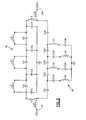
- FIG. 2A preferred form of circuit which embodies the invention is shown in schematic form in FIG. 2 .
- Signals on input line 10pass through inductor L 01 .
- Lowpass filter 16 and highpass filter 18are shown as forming the upper and lower legs, respectively, of the circuit.
- Lowpass filter 16consists of inductors L 1 through L 5 and capacitors C 1 through C 7 .
- Highpass filter 18consists of inductors L 02 through L 05 and capacitors C 01 through C 09 .
- Signals which pass through one or the other of filters 14 and 16pass through inductor L 06 to output line 24 .
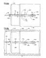
- FIGS. 3 a and 3 bA physical layout of the components forming bandstop filter 22 on top and bottom surfaces of circuit board 26 is shown in FIGS. 3 a and 3 b , respectively.
- the components forming lowpass circuit 16namely, inductors L 1 -L 5 and capacitors C 1 -C 7 , are shown in FIG. 3 a , together with grounding buses 26 a and 26 b and the electrical paths or traces on circuit board 26 connecting the components to one another and to grounding bus 26 a . Shown in FIG.
- 3 bare the components forming highpass circuit 18 , namely, inductors L 02 -L 05 and capacitors C 01 -C 09 , together with grounding buses 26 c and 26 d , input and output inductors L 01 and L 06 , respectively, and conducting pads 26 e and 26 f for connection to the circuit of the usual male and female connectors (not shown).
- Lowpass filter 16consists of three sections, the first formed by inductor L 2 and capacitor C 2 , the second by inductor L 3 and capacitor C 4 and the third by inductor L 4 and capacitor C 6 . These sections are connected to grounding bus 26 a by electrical paths P 1 , P 2 , P 3 and P 4 through parallel capacitors C 1 , C 3 , C 5 and C 7 , respectively.
- Highpass filter 18consists of four sections, the first formed by capacitor C 02 and inductor L 02 , the second by inductor L 03 and capacitor C 04 , the third by capacitor C 06 and inductor L 04 and the forth by inductor L 05 and capacitor C 08 .
- Grounding buses 26 a and 26 care at ground potential, preferably by direct communication with a housing (not shown) wherein circuit board 26 and the circuit components thereof are mounted. Details of such a housing and the manner of grounding connection thereto of grounding buses 26 a and 26 c , as well as a discussion of the preferred presence of grounding buses 26 b and 26 d in spite of their non-functionality in the electrical circuit, may be found in companion application Ser. No.
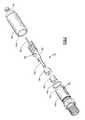
- FIG. 4an embodiment of a complete filter assembly, denoted generally by reference numeral 30 , incorporating circuit 22 on board 26 .
- Assembly 30includes a filter circuit having a plurality of components (inductors, capacitors, etc.), collectively indicated by numeral 32 .
- Circuit components 32are mounted by conventional surface mount techniques upon printed circuit board 26 .
- Female connector assembly 34 and male connector 36are each attached at one end to board 26 in electrical communication with the circuit formed by components 32 . Both the structure and manner of connection of the male and female connectors to the circuit board are entirely conventional.
- Female connector assembly 34extends, with force fit, through openings in deformable rubber seal 38 and insulator 40 .
- Male connector 36extends, with force fit, through an opening in insulator 42 .
- the circuit board with attached connectors, together with insulators and sealare mounted within a housing formed by inner and outer portions 44 and 46 , respectively, each being in the form of a hollow cylinder, preferably having a 0.820 inch diameter or less.
- O-ring 48is received in groove 50 in inner portion 44 and serves as a moisture resistant seal between portions 44 and 46 when assembled.
- FIG. 5Prior to the final assembly operation.
- seal 38 and insulator 40have been inserted into inner portion 44 and insulator 42 has been inserted within outer portion 46 in the positions indicated.
- Circuit board 26has been inserted into inner portion 44 with female connector assembly 34 extending through the opening in seal 38 and into the opening in insulator 40 .
- inner portion 44includes a pair of open slots 52 and 54 extending from open ends 52 a and 54 a , respectively, at one end of inner portion 44 to closed ends 52 b and 54 b , respectively.
- Slot 52has opposing, spaced edges 52 c and 52 d
- slot 54has opposing, spaced edges 54 c and 54 d.
- Circuit board 26is shown in greater detail in the orthographic projection of FIGS. 7 a - 7 c .
- board 26includes relatively wide and narrow, integral portions 26 a and 26 b , respectively, each having substantially parallel side edges spaced equally from central axis A—A.
- Strips of thin, copper foil 26 c and 26 dare securely adhered to what is termed the top surface (FIG. 7 b ) of board 26 in lateral edge portions bordering the side edges of portion 26 a , and like strips 26 e and 26 f are secured to lateral edge portions of the bottom surface.
- these stripsare in electrical communication with the circuit formed by components 32 and serve as grounding buses for the circuit.
- Small raised portions, or “bumps”are provided on each of strips 26 c , 26 d , 26 e and 26 f .
- one bumpis provided on each of the strips, reference numerals 26 c′ , 26 d′ , 26 e′ and 26 f′ denoting the bumps on strips 26 c , 26 d , 26 e and 26 f , respectively.
- More than one bumpmay be provided on any or all strips, if desired, but it is preferred that at least one bump be provided on each strip near the end thereof at the juncture between portions 26 a and 26 b .
- the bumpsare of conductive material, and may conveniently be deposited as small drops of solder.
- inner portion 44When board 26 has been inserted into inner portion 44 the lateral edge portions of wider portion 26 a are positioned in slots 52 and 54 , and extend substantially the full length of the slots.
- inner portion 44has an outside diameter OD 1 over the major portion of its length and a somewhat smaller diameter OD 2 over a portion at the end at which the open ends of slots 52 and 54 are formed.
- the width of board portion 26 ais slightly less than diameter OD 2 but larger than the inside diameter ID 1 of the part of portion 44 which includes slots 52 and 54 .
- Bevel 44 ais formed about the periphery of the end of portion 44 bordering OD 2
- bevel 44 bis formed about the periphery of the shoulder at the junction of the two outside diameters.
- inner and outer portions 44 and 46are shown in axially aligned relation, before and after the final assembly step of forcing the outer over the inner portion.
- the inside diameter ID 2 of portion 46is larger than OD 2 but smaller than OD 1 of portion 44 .
- Bevel 46 a(FIGS. 4 and 5) is formed about the periphery of the end of outer section 46 bordering ID 2 .
- Bevels 44 a and 46 atogether with the fact that OD 2 is less than ID 2 (by a few thousands of an inch) facilitate mating engagement of section 44 and 46 over the axial length of the part of inner portion 44 of diameter OD 2 .
- Bevels 44 b and 46 afacilitate axial alignment of portions 44 and 46 as they are forced into telescopically engaged relation.
- the difference in diameters OD 1 and ID 2is preferably great enough to require the use of an arbor press, or other appropriate tool, to effect relative axial movement of the two sections into full engagement, as seen in FIG. 8 b .
- This interference fitresults in some degree of radially inward deformation of the slotted part of inner portion 44 in the fully assembled condition.
- the spacing of opposing edges 52 c and 52 di.e., the width of slot 52 , denoted by dimension W 1 is greater than the thickness T 1 of the portion of board 26 which is positioned between the slot edges, and is about the same as thickness T 2 in the area of bumps 26 c′ and 26 e′ .
- dimension W 1is greater than the thickness T 1 of the portion of board 26 which is positioned between the slot edges, and is about the same as thickness T 2 in the area of bumps 26 c′ and 26 e′ .
- slot 52After assembly, as seen in FIG. 8 b , the interference fit with outer portion 46 has caused slot 52 to narrow, i.e. opposing edges 52 c and 52 d are closer together and engage the surfaces of strips 26 c and 26 e .
- the amount of inward movement of the slot edgesis greatest, of course, at the open end of the slot.
- the width near the open ends of the slotsis indicated in FIG. 8 b by dimension W 2 ( ⁇ W 1 ).
- circuit board 26is narrower than the outside diameter of the inner portion to avoid. possibly damaging compression by interference fit of the board with the inside diameter of the outer portion.
- the circuit boardis captured with a high pressure contact from the copper ground bus to the inner housing portion along a sufficient length on each side of the circuit components to ensure adequate isolation from inductance and resistance parasitics for proper circuit operation, particularly at frequencies above about 300 Mhz.
- the compressive engagement of O-ring 48 between portions 44 and 46effectively prevents ingress of moisture or foreign matter in the housing.
- the bandstop filter of the present inventionprovides a number of advantages over conventional bandstop filters, among which are improved insertion and return loss. Since the high and low frequency signals are divided and pass, respectively, through highpass and lowpass filters before being recombined, the filter is of the frequency-selective type, thereby reducing the losses. Furthermore, the bandstop filter is implemented in an embodiment using fewer components than the conventional bandstop filter. Also, by using surface mount components with the highpass and lowpass filter components mounted on opposite sides of a single circuit board, the bandstop filter is embodied in an extremely compact physical package. A fully operational bandstop filter of the present invention may be realized by mounting commercially available inductors and capacitors in the configuration shown in FIGS.
- a housing or casing wherein the board and components mounted thereon are containedmay be designed in extremely small versions and in a variety of configurations, such as that of FIGS. 4-8 b and others described in previously mentioned companion application Ser. No. 10/309,375.
Landscapes
- Engineering & Computer Science (AREA)
- Multimedia (AREA)
- Signal Processing (AREA)
- Filters And Equalizers (AREA)
- Networks Using Active Elements (AREA)
- Cable Transmission Systems, Equalization Of Radio And Reduction Of Echo (AREA)
Abstract
Description
The present invention relates to filter circuits of the type used in cable television (CATV) applications, and more specifically to bandstop filters.
A diplex circuit, or more simply a “diplexer,” is a device which separates or combines RF signals. It has been found expedient to utilize diplexers in connection with CATV equipment in a number of situations, some of which use two diplexers back-to-back. These include step attenuators, power bypass circuits, cable simulators and equalizer circuits. Many of the prior art CATV diplex circuits are used to act on signals traveling in so-called forward and return paths, e.g., relatively high frequency RF signals pass from a source of such signals to a television set at subscriber premises in the forward direction over one leg of the circuit while lower frequency (DC) signals pass from the premises in the return direction.
Bandstop or “notch” filters are commonly employed in the CATV industry to block transmission of signals in a specified frequency range. For example, certain channels may be designated as premium channels, requiring payment of a fee from the subscriber in order to receive the signals carrying information representing such channels. If the service is not ordered, i.e., the fee is not paid, an appropriate filter is installed in the cable line coming into the non-paying premises. This is but one of the more traditional uses of bandstop filters, i.e., as a so-called trap. A more recent example is the aforementioned use in the handling of forward and return path signals between a headend and subscriber facilities.
It is desirable that bandstop filters be as compact as possible commensurate with quality performance of their intended function. It is also desirable, of course, that the filters be as inexpensive as possible, again while maintaining high performance criteria. Passband insertion and return loss is of critical importance in such filters, particularly in the digital signal market, which is steadily growing in significance.
It is an object of the present invention to provide a bandstop filter of smaller size than prior art filters offering the same level of performance.
Another object is to provide a bandstop filter for CATV applications which requires a smaller number of components than prior art filters of comparable capabilities.
A further object is to provide a bandstop filter with improved passband insertion and return loss.
It is a principal object to provide a bandstop filter for the CATV industry which incorporates all of the above advantages, i.e., achieving economics of both size and cost while still realizing improved performance.
Other objects will in part be obvious and will in part appear hereinafter.
In accordance with the foregoing objectives, the bandstop filter of the invention two diplexers, back-to-back, in series. A single input line carries signals in a frequency range of , e.g., 0-3 GHz, to a node connected to each of a highpass and a lowpass filter, in parallel. Only signals having a frequency above a first, predetermined value pass through the highpass filter, and only signals having a frequency below a second, predetermined value pass through the lowpass filter. The first and second values are chosen so that a predetermined range of frequencies, i.e., the range or band of frequencies below the first and above the second value, is “stopped” from passing to the single output line. Thus, the RF signals are divided by the first diplexer between those at frequencies which pass the highpass and those which pass the lowpass filters. The outputs of the high and lowpass filters are connected at a second node to form a second diplexer having an output including only signals having frequency values which pass the high and lowpass filters. Frequencies between those passed by the high and lowpass filters do not appear at the output, thereby providing the bandstop. The diplexers are frequency selective, resulting in lower insertion loss due to frequency isolation of the two output ports.
By implementing this circuitry with surface mount technology the bandstop filter of the invention requires fewer components than conventional filters of the same type and level of performance. This means, of course, that the filter of the invention may be fabricated in smaller size and at lower cost than comparable prior art filters. In the preferred embodiment, the components are of the surface mount type with the components forming the highpass and lowpass filters mounted on opposite sides of a single printed circuit board. The circuit also exhibits improved passband insertion and return loss, which is a particularly important feature in the digital signal market.
The foregoing and other features of construction and operation of the bandstop filter of the invention will be more readily understood and fully appreciated from the following detailed disclosure, taken in conjunction with the accompanying drawings.
FIG. 1 is an illustrative flow or block diagram of the circuit of the invention;
FIG. 2 is an electrical schematic of a circuit providing the features of the diagram of FIG. 1;
FIGS. 3aand3bare top and bottom plan views of a printed circuit board with components forming the circuit of FIG. 2 mounted thereon by surface mount techniques;
FIG. 4 is an exploded perspective view of a filter assembly incorporating the printed circuit board of FIGS. 3aand3b;
FIG. 5 is a side elevational view of the filter assembly of FIG. 4 in axial cross section in an intermediate stage of assembly;
FIG. 6 is an enlarged, fragmentary, perspective view of the inner housing section of the assembly, with the circuit board and male connector shown in phantom lines;
FIGS. 7a,7band7care side elevational, top plan, and end elevational views, respectively, providing an orthogonal projection of the circuit board and connectors; and
FIGS. 8aand8bare fragmentary, elevational views, partly in section, of portions of the assembly in successive stages of assembly.
Referring now to FIG. 1 of the drawings,input line 10 carries signals which may range in frequency from 0 to 3 GHZ. All signals enternode 12 offirst diplexer 14 where they are divided between an upper leg of the circuit, formed bylowpass filter 16, and a lower leg, formed byhighpass filter 18.Filters highpass filter 18. This frequency above which signals are passed byfilter 18 is indicated in the drawing as Fp4. Likewise, signals having a frequency value below a second, predetermined level will pass throughlowpass filter 16. This frequency below which signals are passed byfilter 16 is indicated as Fp1. Signals having a frequency above Fs2 (equal to or slightly greater than Fp1) are stopped or blocked, as are signals having a frequency below Fs3 (equal to or slightly less than Fp4). Signals passing throughfilters node 20 ofsecond diplexer 22 and are carried byoutput line 24. The graphical representations in FIG. 1 indicate generally the energy levels of signals at the indicated frequencies. As is apparent, essentially all signals having frequencies below Fp1 and above Fp4 will be passed to the output, while those between Fs2 and Fs3 will reflectively be blocked, thereby providingbandstop filter 26. It will be understood, of course, that representation ofbandstop filter 26 in FIG. 1 does not imply the existence of another filter circuit inoutput line 24, but simply illustrates the fact that signals having frequencies below Fp1 and above Fp4 appear on the output line with signals in the frequency band between Fp1 and Fp4 are stopped.
A preferred form of circuit which embodies the invention is shown in schematic form in FIG.2. Signals oninput line 10 pass through inductor L01.Lowpass filter 16 andhighpass filter 18 are shown as forming the upper and lower legs, respectively, of the circuit.Lowpass filter 16 consists of inductors L1 through L5 and capacitors C1 through C7.Highpass filter 18 consists of inductors L02 through L05 and capacitors C01 through C09. Signals which pass through one or the other offilters output line 24.
A physical layout of the components formingbandstop filter 22 on top and bottom surfaces ofcircuit board 26 is shown in FIGS. 3aand3b, respectively. The components forminglowpass circuit 16, namely, inductors L1-L5 and capacitors C1-C7, are shown in FIG. 3a, together with groundingbuses circuit board 26 connecting the components to one another and to groundingbus 26a. Shown in FIG. 3bare the components forminghighpass circuit 18, namely, inductors L02-L05 and capacitors C01-C09, together with groundingbuses pads
In FIG. 4 is shown an embodiment of a complete filter assembly, denoted generally byreference numeral 30, incorporatingcircuit 22 onboard 26.Assembly 30 includes a filter circuit having a plurality of components (inductors, capacitors, etc.), collectively indicated bynumeral 32.Circuit components 32 are mounted by conventional surface mount techniques upon printedcircuit board 26.Female connector assembly 34 andmale connector 36 are each attached at one end to board26 in electrical communication with the circuit formed bycomponents 32. Both the structure and manner of connection of the male and female connectors to the circuit board are entirely conventional.Female connector assembly 34 extends, with force fit, through openings indeformable rubber seal 38 andinsulator 40.Male connector 36 extends, with force fit, through an opening ininsulator 42.
The circuit board with attached connectors, together with insulators and seal are mounted within a housing formed by inner andouter portions ring 48 is received ingroove 50 ininner portion 44 and serves as a moisture resistant seal betweenportions insulator 40 have been inserted intoinner portion 44 andinsulator 42 has been inserted withinouter portion 46 in the positions indicated.Circuit board 26 has been inserted intoinner portion 44 withfemale connector assembly 34 extending through the opening inseal 38 and into the opening ininsulator 40. As best seen in FIG. 6,inner portion 44 includes a pair ofopen slots inner portion 44 to closed ends52band54b, respectively.Slot 52 has opposing, spacededges slot 54 has opposing, spacededges
Whenboard 26 has been inserted intoinner portion 44 the lateral edge portions ofwider portion 26aare positioned inslots inner portion 44 has an outside diameter OD1 over the major portion of its length and a somewhat smaller diameter OD2 over a portion at the end at which the open ends ofslots board portion 26ais slightly less than diameter OD2 but larger than the inside diameter ID1 of the part ofportion 44 which includesslots Bevel 44ais formed about the periphery of the end ofportion 44 bordering OD2, andbevel 44bis formed about the periphery of the shoulder at the junction of the two outside diameters.
Referring now to FIGS. 8aand8b, inner andouter portions portion 46 is larger than OD2 but smaller than OD1 ofportion 44.Bevel 46a(FIGS. 4 and 5) is formed about the periphery of the end ofouter section 46 bordering ID2.Bevels section inner portion 44 of diameter OD2.Bevels portions inner portion 44 in the fully assembled condition. Prior to assembly of the two portions, as shown in FIG. 8a, the spacing of opposingedges slot 52, denoted by dimension W1 is greater than the thickness T1 of the portion ofboard 26 which is positioned between the slot edges, and is about the same as thickness T2 in the area ofbumps 26c′ and26e′. The same is true, of course, with respect to slot54.
After assembly, as seen in FIG. 8b, the interference fit withouter portion 46 has causedslot 52 to narrow, i.e. opposingedges strips slot 52 approaches closedend 52b, it is nevertheless sufficient to cause the slot edges to engagebumps 26c′ and26e′. Thus, a very solid and reliable ground path along substantially the entire length of groundingbuses Circuit board 26 is narrower than the outside diameter of the inner portion to avoid. possibly damaging compression by interference fit of the board with the inside diameter of the outer portion. The circuit board is captured with a high pressure contact from the copper ground bus to the inner housing portion along a sufficient length on each side of the circuit components to ensure adequate isolation from inductance and resistance parasitics for proper circuit operation, particularly at frequencies above about 300 Mhz. The compressive engagement of O-ring 48 betweenportions
From the foregoing it will be appreciated that the bandstop filter of the present invention provides a number of advantages over conventional bandstop filters, among which are improved insertion and return loss. Since the high and low frequency signals are divided and pass, respectively, through highpass and lowpass filters before being recombined, the filter is of the frequency-selective type, thereby reducing the losses. Furthermore, the bandstop filter is implemented in an embodiment using fewer components than the conventional bandstop filter. Also, by using surface mount components with the highpass and lowpass filter components mounted on opposite sides of a single circuit board, the bandstop filter is embodied in an extremely compact physical package. A fully operational bandstop filter of the present invention may be realized by mounting commercially available inductors and capacitors in the configuration shown in FIGS. 3aand3bon a circuit board having an area of about 250 square millimeters on each surface, although it will be understood that design options using both larger and smaller boards are possible within the scope of the invention. Consequently, a housing or casing wherein the board and components mounted thereon are contained may be designed in extremely small versions and in a variety of configurations, such as that of FIGS. 4-8band others described in previously mentioned companion application Ser. No. 10/309,375.
Claims (22)
1. A bandstop filter for CATV applications having an input for receiving signals having frequencies in a predetermined range and an output carrying signals having frequencies below a first value within said range and above a second value, higher than said first value, within said range with signals having frequencies between said first and second values being blocked from reaching said output, said filter comprising:
a) a first diplexer to which said input is connected at a first node;
b) a lowpass filter having a first input end connected to said first node and a first output end, said lowpass filter having components between said first input and output ends which pass signals having frequencies below said first value and block signals having frequencies above said first value;
c) a highpass filter having a second input end connected to said first node and a second output end, said highpass filter having components between said second input and output ends which pass signals having frequencies above said second value and block signals having frequencies below said second value; and
d) a second diplexer having a second node to which said first output end of said lowpass filter, said second output end of said highpass filter and said output are all connected.
2. The bandstop filter ofclaim 1 wherein said components of each of said lowpass and highpass filters comprise a plurality of inductors and capacitors.
3. The bandstop filter ofclaim 2 wherein said components are all of the surface mount type and are mounted on a single printed circuit board.
4. The bandstop filter ofclaim 3 wherein said circuit board has opposite, major surfaces and said components of said lowpass filter are mounted upon one surface and said components of said highpass filter are mounted upon the opposite surface of said printed circuit board.
5. The bandstop filter ofclaim 3 and further including a housing and means for mounting said circuit board within said housing.
6. The bandstop filter ofclaim 5 and further including a secure grounding connection between said components and said housing.
7. The bandstop filter ofclaim 6 wherein said housing has a diameter of no greater than 0.820 inches.
8. The bandstop filter ofclaim 6 wherein said grounding connection comprises at least one elongated grounding bus on said circuit board which is in electrical communication with said housing over substantially the full length of said grounding bus.
9. The bandstop filter ofclaim 5 wherein said housing includes two portions which are mutually joined by a force fit of one of said portions into the other.
10. The bandstop filter ofclaim 9 wherein said two portions form a hollow, substantially cylindrical structure.
11. The bandstop filter ofclaim 10 wherein said force fit compresses one of said two portions into electrical communication with each of said lowpass and highpass filters.
12. The bandstop filter ofclaim 11 wherein said circuit board has opposite, major surfaces, said components of said lowpass filter are mounted upon one surface and said components of said highpass filter are mounted upon the opposite surface of said printed circuit board, and further including a first grounding bus mounted upon said one surface and electrically communicating with said lowpass filter and with said housing, and a second grounding bus mounted upon said opposite surface and electrically communicating with said highpass filter and with said housing.
13. The bandstop filter ofclaim 11 wherein said circuit board includes first and second, parallel, elongated edges, and said first and second grounding buses extend along said first and second edges, respectively.
14. A bandstop filter for CATV applications comprising:
a) a signal input terminal for receiving RF signals having frequencies in a predetermined range;
b) first filter means for receiving signals from said input terminal and passing to a first filter output signals having frequencies below a first value within said predetermined range and blocking signals having frequencies above said first value;
c) second filter means for receiving signals from said input terminal and passing to a second filter output signals having frequencies above a second value, higher than said first value, within said predetermined range and blocking signals having frequencies below said second value, whereby said RF signals from said input terminal are separated by said first and second filter means into different frequency bands; and
d) a signal output terminal connected to both said first and second outputs, whereby said RF signals which pass said first and second filter means are combined at said output terminal.
15. The bandstop filter ofclaim 14 wherein said first filter means comprise a lowpass filter.
16. The bandstop filter ofclaim 15 wherein said second filter means comprise a highpass filter.
17. The bandstop filter ofclaim 16 wherein said first and second filter means each comprise a plurality of inductors and capacitors.
18. The bandstop filter ofclaim 17 wherein all of said inductors and capacitors are surface mounted upon a single printed circuit board.
19. The bandstop filter ofclaim 18 wherein said inductors and capacitors of said first filter means are mounted on one surface of said board and said inductors and capacitors of said second filter means are mounted on the opposite surface of said board.
20. The method of communicating RF signals having frequencies below a first value and above a second value while blocking signals having frequencies between said first and second values, said method comprising:
a) connecting a first plurality of electronic components to form a first filter circuit having a first input and a first output, said first filter circuit being operative to pass RF signals applied to said first input which have frequencies below a first value and to block signals having frequencies above said first value;
b) connecting a second plurality of electronic components to form a second filter circuit having a second input and a second output, said second filter circuit being operative to pass RF signals applied to said second input which have frequencies above a second value, higher than said first value, and to block signals having frequencies below said second value;
c) connecting said first and second inputs and a single input line carrying RF signals together at a first node to form a first diplexer; and
d) connecting said first and second outputs and a single output line together at a second node to form a second diplexer, whereby said first and second filter circuits are connected in parallel and said first and second diplexers are in series.
21. The method ofclaim 20 wherein said diplexers are frequency selective.
22. The method ofclaim 20 wherein said first and second pluralities of electronic components are surface mounted upon first and second, opposite surfaces, respectively, of a single printed circuit board.
Priority Applications (4)
| Application Number | Priority Date | Filing Date | Title |
|---|---|---|---|
| US10/309,376US6737935B1 (en) | 2002-12-03 | 2002-12-03 | Diplex circuit forming bandstop filter |
| CA002426614ACA2426614C (en) | 2002-12-03 | 2003-04-25 | Diplex circuit forming bandstop filter |
| BR0301710-9ABR0301710A (en) | 2002-12-03 | 2003-06-17 | Band Lock Filter for Cable Television Applications and Method of Communicating Radio Frequency Signals |
| MXPA03010619AMXPA03010619A (en) | 2002-12-03 | 2003-11-19 | Diplex circuit forming bandstop filter. |
Applications Claiming Priority (1)
| Application Number | Priority Date | Filing Date | Title |
|---|---|---|---|
| US10/309,376US6737935B1 (en) | 2002-12-03 | 2002-12-03 | Diplex circuit forming bandstop filter |
Publications (2)
| Publication Number | Publication Date |
|---|---|
| US6737935B1true US6737935B1 (en) | 2004-05-18 |
| US20040104786A1 US20040104786A1 (en) | 2004-06-03 |
Family
ID=32298092
Family Applications (1)
| Application Number | Title | Priority Date | Filing Date |
|---|---|---|---|
| US10/309,376Expired - LifetimeUS6737935B1 (en) | 2002-12-03 | 2002-12-03 | Diplex circuit forming bandstop filter |
Country Status (4)
| Country | Link |
|---|---|
| US (1) | US6737935B1 (en) |
| BR (1) | BR0301710A (en) |
| CA (1) | CA2426614C (en) |
| MX (1) | MXPA03010619A (en) |
Cited By (31)
| Publication number | Priority date | Publication date | Assignee | Title |
|---|---|---|---|---|
| US20040104788A1 (en)* | 1999-08-24 | 2004-06-03 | Tresness Andrew F. | Electronic filter assembly |
| US20080204166A1 (en)* | 2007-02-22 | 2008-08-28 | Shafer Steven K | Dual Bandstop Filter With Enhanced Upper Passband Response |
| US20080303610A1 (en)* | 2007-06-07 | 2008-12-11 | Eagle Comtronics, Inc. | Tuned filters with enhanced high frequency response |
| US20090015350A1 (en)* | 2007-07-09 | 2009-01-15 | John Mezzalingua Associates, Inc. | Band-stop filters |
| US20090027139A1 (en)* | 2005-09-28 | 2009-01-29 | Epcos Ag | Band-pass filter |
| WO2009029408A1 (en)* | 2007-08-29 | 2009-03-05 | Greatbatch Ltd. | Cylindrical bandstop filters for medical lead systems |
| US20100109799A1 (en)* | 2008-11-04 | 2010-05-06 | Richard K Karlquist | Split Band Signal Processing |
| US20100117653A1 (en)* | 2008-11-12 | 2010-05-13 | Ralph Oppelt | Diplex filter and method to filter signals |
| US20100127795A1 (en)* | 2007-05-29 | 2010-05-27 | Thomas Bauer | Multiband Filter |
| US20100231327A1 (en)* | 2006-11-09 | 2010-09-16 | Greatbatch Ltd. | Capacitor and inductor elements physically disposed in series whose lumped parameters are electrically connected in parallel to form a bandstop filter |
| US20110085584A1 (en)* | 2008-05-23 | 2011-04-14 | Hangzhou H3C Technologies Co., Ltd. | Long-reach ethernet system and relay |
| CN102064786A (en)* | 2009-11-16 | 2011-05-18 | 国基电子(上海)有限公司 | Band-pass filter |
| US20110187481A1 (en)* | 2010-02-01 | 2011-08-04 | John Mezzalingua Associates, Inc. | Multipath mitigation circuit for home network |
| US20120212305A1 (en)* | 2011-02-21 | 2012-08-23 | John Mezzalingua Associates, Inc. | Filter circuit and method of tuning filter circuit |
| US8479247B2 (en) | 2010-04-14 | 2013-07-02 | Ppc Broadband, Inc. | Upstream bandwidth conditioning device |
| US8510782B2 (en) | 2008-10-21 | 2013-08-13 | Ppc Broadband, Inc. | CATV entry adapter and method for preventing interference with eMTA equipment from MoCA Signals |
| US8561125B2 (en) | 2010-08-30 | 2013-10-15 | Ppc Broadband, Inc. | Home network frequency conditioning device and method |
| CN103997309A (en)* | 2013-02-15 | 2014-08-20 | 株式会社村田制作所 | Polar-type low pass filter and demultiplexer equipped therewith |
| US9167286B2 (en) | 2009-09-21 | 2015-10-20 | Ppc Broadband, Inc. | Passive multi-port entry adapter and method for preserving downstream CATV signal strength within in-home network |
| US20150365732A1 (en)* | 2014-06-12 | 2015-12-17 | Eagle Comtronics, Inc. | Legacy converter filter with extended frequency range |
| US9363469B2 (en) | 2008-07-17 | 2016-06-07 | Ppc Broadband, Inc. | Passive-active terminal adapter and method having automatic return loss control |
| US20160261729A1 (en)* | 2015-03-05 | 2016-09-08 | Wisol Co., Ltd. | Filter module |
| US9461611B2 (en) | 2013-09-27 | 2016-10-04 | Murata Manufacturing Co., Ltd. | Low pass filter having attenuation pole and wave splitter |
| US9516774B2 (en) | 2006-08-25 | 2016-12-06 | Ppc Broadband, Inc. | Outer sleeve for CATV filter |
| US9647851B2 (en) | 2008-10-13 | 2017-05-09 | Ppc Broadband, Inc. | Ingress noise inhibiting network interface device and method for cable television networks |
| US10021343B2 (en) | 2010-12-21 | 2018-07-10 | Ppc Broadband, Inc. | Method and apparatus for reducing isolation in a home network |
| US10142677B2 (en) | 2008-10-21 | 2018-11-27 | Ppc Broadband, Inc. | Entry device for a CATV network |
| US10212392B2 (en) | 2016-06-30 | 2019-02-19 | Ppc Broadband, Inc. | Passive enhanced MoCA entry device |
| US11076191B2 (en) | 2018-01-19 | 2021-07-27 | Ppc Broadband, Inc. | Systems and methods for extending an in-home splitter network |
| US20220416389A1 (en)* | 2021-06-29 | 2022-12-29 | Ezconn Corporation | Coaxial isolator |
| US11910052B2 (en) | 2008-10-21 | 2024-02-20 | Ppc Broadband, Inc. | Entry device for communicating external network signals and in-home network signals |
Families Citing this family (1)
| Publication number | Priority date | Publication date | Assignee | Title |
|---|---|---|---|---|
| US8763063B2 (en)* | 2004-06-01 | 2014-06-24 | Time Warner Cable Enterprises Llc | Controlled isolation splitter apparatus and methods |
Citations (25)
| Publication number | Priority date | Publication date | Assignee | Title |
|---|---|---|---|---|
| US2462491A (en) | 1945-10-22 | 1949-02-22 | Hallett Mfg Company | Ignition coil and filter shield assembly |
| US3579154A (en) | 1969-04-23 | 1971-05-18 | Collins Radio Co | Vhf filter having absorptive tuned section to eliminate narrow spurious passband |
| US3806813A (en) | 1972-06-26 | 1974-04-23 | Gte Sylvania Inc | Filter system for amplifier station for amplifying signals in separate frequency bands |
| US3956717A (en) | 1974-08-01 | 1976-05-11 | Wideband Services, Inc. | Hybrid diplexing filter |
| US4100516A (en) | 1977-03-18 | 1978-07-11 | The Bendix Corporation | Microwave circuit having grounding structure |
| US4701726A (en) | 1985-12-03 | 1987-10-20 | Northeast Filter Co., Inc. | Trap filter assembly |
| US4783639A (en) | 1985-11-21 | 1988-11-08 | Hughes Aircraft Company | Wideband microwave diplexer including band pass and band stop resonators |
| US4954790A (en) | 1989-11-15 | 1990-09-04 | Avantek, Inc. | Enhanced coupled, even mode terminated baluns, and mixers and modulators constructed therefrom |
| US4963966A (en) | 1989-12-04 | 1990-10-16 | Scientific Atlanta, Inc. | CATV distribution system, especially adapted for off-premises premium channel interdiction |
| US5150087A (en) | 1989-11-30 | 1992-09-22 | Mitsumi Electric Co., Ltd. | Electrical signal filter and method for manufacture of electrical signal filter internal circuit board |
| US5278525A (en) | 1992-06-11 | 1994-01-11 | John Mezzalingua Assoc. Inc. | Electrical filter with multiple filter sections |
| US5304967A (en) | 1991-02-05 | 1994-04-19 | Tdk Corporation | Multi-layer circuit board dielectric filter having a plurality of dielectric resonators |
| US5548255A (en) | 1995-06-23 | 1996-08-20 | Microphase Corporation | Compact diplexer connection circuit |
| US5745838A (en) | 1997-03-14 | 1998-04-28 | Tresness Irrevocable Patent Trust | Return path filter |
| US5793265A (en) | 1997-05-30 | 1998-08-11 | Microphase Corporation | Compact diplexer |
| US5815052A (en) | 1995-05-31 | 1998-09-29 | Murata Manufacturing Co., Ltd. | High-frequency composite components comprising first and second circuits connected in parallel for multi-frequency systems |
| US5821831A (en)* | 1996-05-10 | 1998-10-13 | Eagle Comtronics, Inc. | Diplex filter comprising monotonic poles |
| US5881362A (en)* | 1994-11-30 | 1999-03-09 | General Instrument Corporation Of Delaware | Method of ingress noise reduction in calbe return paths |
| US5898406A (en) | 1997-03-13 | 1999-04-27 | Nokia Mobile Phones Limited | Antenna mounted diplexer |
| US5906512A (en) | 1995-07-18 | 1999-05-25 | The Whitaker Corporation | Electronics box coaxial connection assembly |
| US5999796A (en) | 1997-03-14 | 1999-12-07 | Tresness Irrevocable Patent Trust | Return path attenuation filter |
| US6031432A (en) | 1997-02-28 | 2000-02-29 | Schreuders; Ronald C. | Balancing apparatus for signal transmissions |
| US6177849B1 (en) | 1998-11-18 | 2001-01-23 | Oneline Ag | Non-saturating, flux cancelling diplex filter for power line communications |
| US6191666B1 (en) | 1999-03-25 | 2001-02-20 | Industrial Technology Research Institute | Miniaturized multi-layer ceramic lowpass filter |
| US6252474B1 (en)* | 1997-12-26 | 2001-06-26 | Nec Corporation | Semiconductor phase shifter having high-pass signal path and low-pass signal path connected in parallel |
- 2002
- 2002-12-03USUS10/309,376patent/US6737935B1/ennot_activeExpired - Lifetime
- 2003
- 2003-04-25CACA002426614Apatent/CA2426614C/ennot_activeExpired - Lifetime
- 2003-06-17BRBR0301710-9Apatent/BR0301710A/ennot_activeIP Right Cessation
- 2003-11-19MXMXPA03010619Apatent/MXPA03010619A/enactiveIP Right Grant
Patent Citations (25)
| Publication number | Priority date | Publication date | Assignee | Title |
|---|---|---|---|---|
| US2462491A (en) | 1945-10-22 | 1949-02-22 | Hallett Mfg Company | Ignition coil and filter shield assembly |
| US3579154A (en) | 1969-04-23 | 1971-05-18 | Collins Radio Co | Vhf filter having absorptive tuned section to eliminate narrow spurious passband |
| US3806813A (en) | 1972-06-26 | 1974-04-23 | Gte Sylvania Inc | Filter system for amplifier station for amplifying signals in separate frequency bands |
| US3956717A (en) | 1974-08-01 | 1976-05-11 | Wideband Services, Inc. | Hybrid diplexing filter |
| US4100516A (en) | 1977-03-18 | 1978-07-11 | The Bendix Corporation | Microwave circuit having grounding structure |
| US4783639A (en) | 1985-11-21 | 1988-11-08 | Hughes Aircraft Company | Wideband microwave diplexer including band pass and band stop resonators |
| US4701726A (en) | 1985-12-03 | 1987-10-20 | Northeast Filter Co., Inc. | Trap filter assembly |
| US4954790A (en) | 1989-11-15 | 1990-09-04 | Avantek, Inc. | Enhanced coupled, even mode terminated baluns, and mixers and modulators constructed therefrom |
| US5150087A (en) | 1989-11-30 | 1992-09-22 | Mitsumi Electric Co., Ltd. | Electrical signal filter and method for manufacture of electrical signal filter internal circuit board |
| US4963966A (en) | 1989-12-04 | 1990-10-16 | Scientific Atlanta, Inc. | CATV distribution system, especially adapted for off-premises premium channel interdiction |
| US5304967A (en) | 1991-02-05 | 1994-04-19 | Tdk Corporation | Multi-layer circuit board dielectric filter having a plurality of dielectric resonators |
| US5278525A (en) | 1992-06-11 | 1994-01-11 | John Mezzalingua Assoc. Inc. | Electrical filter with multiple filter sections |
| US5881362A (en)* | 1994-11-30 | 1999-03-09 | General Instrument Corporation Of Delaware | Method of ingress noise reduction in calbe return paths |
| US5815052A (en) | 1995-05-31 | 1998-09-29 | Murata Manufacturing Co., Ltd. | High-frequency composite components comprising first and second circuits connected in parallel for multi-frequency systems |
| US5548255A (en) | 1995-06-23 | 1996-08-20 | Microphase Corporation | Compact diplexer connection circuit |
| US5906512A (en) | 1995-07-18 | 1999-05-25 | The Whitaker Corporation | Electronics box coaxial connection assembly |
| US5821831A (en)* | 1996-05-10 | 1998-10-13 | Eagle Comtronics, Inc. | Diplex filter comprising monotonic poles |
| US6031432A (en) | 1997-02-28 | 2000-02-29 | Schreuders; Ronald C. | Balancing apparatus for signal transmissions |
| US5898406A (en) | 1997-03-13 | 1999-04-27 | Nokia Mobile Phones Limited | Antenna mounted diplexer |
| US5745838A (en) | 1997-03-14 | 1998-04-28 | Tresness Irrevocable Patent Trust | Return path filter |
| US5999796A (en) | 1997-03-14 | 1999-12-07 | Tresness Irrevocable Patent Trust | Return path attenuation filter |
| US5793265A (en) | 1997-05-30 | 1998-08-11 | Microphase Corporation | Compact diplexer |
| US6252474B1 (en)* | 1997-12-26 | 2001-06-26 | Nec Corporation | Semiconductor phase shifter having high-pass signal path and low-pass signal path connected in parallel |
| US6177849B1 (en) | 1998-11-18 | 2001-01-23 | Oneline Ag | Non-saturating, flux cancelling diplex filter for power line communications |
| US6191666B1 (en) | 1999-03-25 | 2001-02-20 | Industrial Technology Research Institute | Miniaturized multi-layer ceramic lowpass filter |
Cited By (79)
| Publication number | Priority date | Publication date | Assignee | Title |
|---|---|---|---|---|
| US6888423B2 (en)* | 1999-08-24 | 2005-05-03 | Arrow Communication Laboratories, Inc. | Electronic filter assembly |
| US20040104788A1 (en)* | 1999-08-24 | 2004-06-03 | Tresness Andrew F. | Electronic filter assembly |
| US20090027139A1 (en)* | 2005-09-28 | 2009-01-29 | Epcos Ag | Band-pass filter |
| US7944327B2 (en)* | 2005-09-28 | 2011-05-17 | Epcos Ag | Band-pass filter having a ring resonator |
| US9516774B2 (en) | 2006-08-25 | 2016-12-06 | Ppc Broadband, Inc. | Outer sleeve for CATV filter |
| US10424893B2 (en) | 2006-08-25 | 2019-09-24 | Ppc Broadband, Inc. | Outer sleeve for CATV filter |
| US11621533B2 (en) | 2006-08-25 | 2023-04-04 | Ppc Broadband, Inc. | Outer sleeve for CATV filter |
| US20100231327A1 (en)* | 2006-11-09 | 2010-09-16 | Greatbatch Ltd. | Capacitor and inductor elements physically disposed in series whose lumped parameters are electrically connected in parallel to form a bandstop filter |
| US7920916B2 (en)* | 2006-11-09 | 2011-04-05 | Greatbatch Ltd. | Capacitor and inductor elements physically disposed in series whose lumped parameters are electrically connected in parallel to form a bandstop filter |
| US7592882B2 (en) | 2007-02-22 | 2009-09-22 | John Mezzalingua Associates, Inc. | Dual bandstop filter with enhanced upper passband response |
| US20080204166A1 (en)* | 2007-02-22 | 2008-08-28 | Shafer Steven K | Dual Bandstop Filter With Enhanced Upper Passband Response |
| US8384496B2 (en) | 2007-05-29 | 2013-02-26 | Epcos Ag | Multiband filter |
| US20100127795A1 (en)* | 2007-05-29 | 2010-05-27 | Thomas Bauer | Multiband Filter |
| US20080303610A1 (en)* | 2007-06-07 | 2008-12-11 | Eagle Comtronics, Inc. | Tuned filters with enhanced high frequency response |
| US7821359B2 (en) | 2007-07-09 | 2010-10-26 | John Messalingua Associates, Inc. | Band-stop filters |
| US20090015350A1 (en)* | 2007-07-09 | 2009-01-15 | John Mezzalingua Associates, Inc. | Band-stop filters |
| WO2009029408A1 (en)* | 2007-08-29 | 2009-03-05 | Greatbatch Ltd. | Cylindrical bandstop filters for medical lead systems |
| US20110085584A1 (en)* | 2008-05-23 | 2011-04-14 | Hangzhou H3C Technologies Co., Ltd. | Long-reach ethernet system and relay |
| US8693497B2 (en)* | 2008-05-23 | 2014-04-08 | Hangzhou H3C Technologies Co., Ltd. | Long-reach ethernet system and relay |
| US9769418B2 (en) | 2008-07-17 | 2017-09-19 | Ppc Broadband, Inc. | Passive-active terminal adapter and method having automatic return loss control |
| US10257462B2 (en) | 2008-07-17 | 2019-04-09 | Ppc Broadband, Inc. | Adapter for a cable-television network |
| US9363469B2 (en) | 2008-07-17 | 2016-06-07 | Ppc Broadband, Inc. | Passive-active terminal adapter and method having automatic return loss control |
| US9647851B2 (en) | 2008-10-13 | 2017-05-09 | Ppc Broadband, Inc. | Ingress noise inhibiting network interface device and method for cable television networks |
| US10154302B2 (en) | 2008-10-13 | 2018-12-11 | Ppc Broadband, Inc. | CATV entry adapter and method for distributing CATV and in-home entertainment signals |
| US10187673B2 (en) | 2008-10-13 | 2019-01-22 | Ppc Broadband, Inc. | Ingress noise inhibiting network interface device and method for cable television networks |
| US10045056B2 (en) | 2008-10-13 | 2018-08-07 | Ppc Broadband, Inc. | Ingress noise inhibiting network interface device and method for cable television networks |
| US11528526B2 (en) | 2008-10-21 | 2022-12-13 | Ppc Broadband, Inc. | Entry device for communicating external network signals and in-home network signals |
| US10154304B2 (en) | 2008-10-21 | 2018-12-11 | Ppc Broadband, Inc. | Methods for controlling CATV signal communication between a CATV network and an in-home network, and preserving downstream CATV signal strength within the in-home network |
| US10917685B2 (en) | 2008-10-21 | 2021-02-09 | Ppc Broadband, Inc. | Entry device for communicating signals between an external network and an in-home network |
| US8510782B2 (en) | 2008-10-21 | 2013-08-13 | Ppc Broadband, Inc. | CATV entry adapter and method for preventing interference with eMTA equipment from MoCA Signals |
| US10419813B2 (en) | 2008-10-21 | 2019-09-17 | Ppc Broadband, Inc. | Passive multi-port entry adapter for preserving downstream CATV signal strength |
| US10142677B2 (en) | 2008-10-21 | 2018-11-27 | Ppc Broadband, Inc. | Entry device for a CATV network |
| US10341719B2 (en) | 2008-10-21 | 2019-07-02 | Ppc Broadband, Inc. | Entry adapter for communicating external signals to an internal network and communicating client signals in the client network |
| US10341718B2 (en) | 2008-10-21 | 2019-07-02 | Ppc Broadband, Inc. | Passive multi-port entry adapter and method for preserving downstream CATV signal strength within in-home network |
| US10149004B2 (en) | 2008-10-21 | 2018-12-04 | Ppc Broadband, Inc. | Entry device and method for communicating CATV signals and MoCA in-home network signals in an entry device |
| US10284904B2 (en) | 2008-10-21 | 2019-05-07 | Ppc Broadband, Inc. | Entry adapters for conducting can signals and in-home network signals |
| US10284903B2 (en) | 2008-10-21 | 2019-05-07 | Ppc Broadband, Inc. | Entry adapters for frequency band blocking internal network signals |
| US10154303B2 (en) | 2008-10-21 | 2018-12-11 | Ppc Broadband, Inc. | Entry adapter that blocks different frequency bands and preserves downstream signal strength |
| US11910052B2 (en) | 2008-10-21 | 2024-02-20 | Ppc Broadband, Inc. | Entry device for communicating external network signals and in-home network signals |
| US8483318B2 (en)* | 2008-11-04 | 2013-07-09 | Agilent Technologies, Inc. | Split band signal processing |
| US20100109799A1 (en)* | 2008-11-04 | 2010-05-06 | Richard K Karlquist | Split Band Signal Processing |
| US8217657B2 (en)* | 2008-11-12 | 2012-07-10 | Siemens Aktiengesellschaft | Diplex filter and method to filter signals |
| US20100117653A1 (en)* | 2008-11-12 | 2010-05-13 | Ralph Oppelt | Diplex filter and method to filter signals |
| US9516376B2 (en) | 2009-09-21 | 2016-12-06 | Ppc Broadband, Inc. | Passive multi-port entry adapter and method for preserving downstream CATV signal strength within in-home network |
| US9860591B2 (en) | 2009-09-21 | 2018-01-02 | Ppc Broadband, Inc. | Passive multi-port entry adapter and method for preserving downstream CATV signal strength within in-home network |
| US9167286B2 (en) | 2009-09-21 | 2015-10-20 | Ppc Broadband, Inc. | Passive multi-port entry adapter and method for preserving downstream CATV signal strength within in-home network |
| US20110115573A1 (en)* | 2009-11-16 | 2011-05-19 | Ambit Microsystems (Shanghai) Ltd. | Band-pass filter |
| CN102064786A (en)* | 2009-11-16 | 2011-05-18 | 国基电子(上海)有限公司 | Band-pass filter |
| CN102064786B (en)* | 2009-11-16 | 2013-11-27 | 国基电子(上海)有限公司 | band pass filter |
| US20110187481A1 (en)* | 2010-02-01 | 2011-08-04 | John Mezzalingua Associates, Inc. | Multipath mitigation circuit for home network |
| US9306530B2 (en) | 2010-02-01 | 2016-04-05 | Ppc Broadband, Inc. | Multipath mitigation circuit for home network |
| US9979373B2 (en) | 2010-02-01 | 2018-05-22 | Ppc Broadband, Inc. | Multipath mitigation circuit for home network |
| US10790793B2 (en) | 2010-02-01 | 2020-09-29 | Ppc Broadband, Inc. | Filter circuit |
| US11444592B2 (en) | 2010-02-01 | 2022-09-13 | Ppc Broadband, Inc. | Filter circuit |
| US8487717B2 (en) | 2010-02-01 | 2013-07-16 | Ppc Broadband, Inc. | Multipath mitigation circuit for home network |
| US10284162B2 (en) | 2010-02-01 | 2019-05-07 | Ppc Broadband, Inc. | Multipath mitigation circuit for home network |
| US8479247B2 (en) | 2010-04-14 | 2013-07-02 | Ppc Broadband, Inc. | Upstream bandwidth conditioning device |
| US8561125B2 (en) | 2010-08-30 | 2013-10-15 | Ppc Broadband, Inc. | Home network frequency conditioning device and method |
| US11070766B2 (en) | 2010-12-21 | 2021-07-20 | Ppc Broadband, Inc. | Method and apparatus for reducing isolation in a home network |
| US10750120B2 (en) | 2010-12-21 | 2020-08-18 | Ppc Broadband, Inc. | Method and apparatus for reducing isolation in a home network |
| US10021343B2 (en) | 2010-12-21 | 2018-07-10 | Ppc Broadband, Inc. | Method and apparatus for reducing isolation in a home network |
| US20120212305A1 (en)* | 2011-02-21 | 2012-08-23 | John Mezzalingua Associates, Inc. | Filter circuit and method of tuning filter circuit |
| US9444424B2 (en)* | 2013-02-15 | 2016-09-13 | Murata Manufacturing Co., Ltd. | Polar-type low pass filter and demultiplexer equipped therewith |
| US20140232481A1 (en)* | 2013-02-15 | 2014-08-21 | Murata Manufacturing Co., Ltd. | Polar-type low pass filter and demultiplexer equipped therewith |
| CN103997309A (en)* | 2013-02-15 | 2014-08-20 | 株式会社村田制作所 | Polar-type low pass filter and demultiplexer equipped therewith |
| TWI654836B (en) | 2013-02-15 | 2019-03-21 | 日商村田製作所股份有限公司 | Polar-type low pass filter and demultiplexer equipped therewith |
| CN103997309B (en)* | 2013-02-15 | 2017-03-01 | 株式会社村田制作所 | There are polar form low pass filter and the demultiplexer including it |
| TWI654835B (en) | 2013-09-27 | 2019-03-21 | 日商村田製作所股份有限公司 | Low pass filter having attenuation pole and wave splitter |
| US9461611B2 (en) | 2013-09-27 | 2016-10-04 | Murata Manufacturing Co., Ltd. | Low pass filter having attenuation pole and wave splitter |
| US9445160B2 (en)* | 2014-06-12 | 2016-09-13 | Eagle Comtronics, Inc. | Legacy converter filter with extended frequency range |
| US20150365732A1 (en)* | 2014-06-12 | 2015-12-17 | Eagle Comtronics, Inc. | Legacy converter filter with extended frequency range |
| US20160261729A1 (en)* | 2015-03-05 | 2016-09-08 | Wisol Co., Ltd. | Filter module |
| US11076129B2 (en) | 2016-06-30 | 2021-07-27 | Ppc Broadband, Inc. | MoCA entry device |
| US10582160B2 (en) | 2016-06-30 | 2020-03-03 | Ppc Broadband, Inc. | MoCA entry device |
| US11647162B2 (en) | 2016-06-30 | 2023-05-09 | Ppc Broadband, Inc. | MoCA entry device |
| US10212392B2 (en) | 2016-06-30 | 2019-02-19 | Ppc Broadband, Inc. | Passive enhanced MoCA entry device |
| US11076191B2 (en) | 2018-01-19 | 2021-07-27 | Ppc Broadband, Inc. | Systems and methods for extending an in-home splitter network |
| US20220416389A1 (en)* | 2021-06-29 | 2022-12-29 | Ezconn Corporation | Coaxial isolator |
| US12206151B2 (en)* | 2021-06-29 | 2025-01-21 | Ezconn Corporation | Coaxial isolator |
Also Published As
| Publication number | Publication date |
|---|---|
| US20040104786A1 (en) | 2004-06-03 |
| CA2426614C (en) | 2006-09-05 |
| CA2426614A1 (en) | 2004-06-03 |
| BR0301710A (en) | 2004-08-24 |
| MXPA03010619A (en) | 2004-10-15 |
Similar Documents
| Publication | Publication Date | Title |
|---|---|---|
| US6737935B1 (en) | Diplex circuit forming bandstop filter | |
| US6380826B1 (en) | Filter assembly | |
| US6794957B2 (en) | CATV filter assembly with improved electrical grounding | |
| US6888423B2 (en) | Electronic filter assembly | |
| US8123563B2 (en) | Electrical connector incorporating passive circuit elements | |
| US6944005B2 (en) | Surge protected coaxial termination | |
| US4701726A (en) | Trap filter assembly | |
| US10811749B2 (en) | Mini isolator | |
| US20050283974A1 (en) | Methods of manufacturing an electrical connector incorporating passive circuit elements | |
| US10868373B2 (en) | Mini isolator | |
| US20100255726A1 (en) | Electrical connector with magnetic module | |
| JPS63128801A (en) | filter | |
| US6894585B2 (en) | High quality factor (Q) planar spiral inductor based CATV diplexer and telephony module | |
| US6784760B2 (en) | Step attenuator using frequency dependent components and method of effecting signal attenuation | |
| JP2003347803A (en) | Bandstop filter and communication device | |
| EP1633023B1 (en) | Filtered connector that blocks high frequency noise | |
| US20030090340A1 (en) | Signal filter | |
| US6873225B2 (en) | Diplexers with low pass filter having distributed and non-distributed (lumped) elements | |
| JP3649584B2 (en) | High frequency electronic equipment | |
| JP2000068717A (en) | Dielectric oscillation parts, dielectric filter, antenna multicoupler, composite filter and communication equipment | |
| JPS58114516A (en) | Mixing circuit | |
| JPH09148143A (en) | Passive device | |
| JPH06276006A (en) | Dielectric filter | |
| JPH0870203A (en) | Filter device including dielectric resonator | |
| JPH0758570A (en) | Lc composite component |
Legal Events
| Date | Code | Title | Description |
|---|---|---|---|
| AS | Assignment | Owner name:JOHN MEZZALINGUA ASSOCIATES, INC., NEW YORK Free format text:ASSIGNMENT OF ASSIGNORS INTEREST;ASSIGNOR:SHAFER, STEVEN;REEL/FRAME:013548/0913 Effective date:20021126 | |
| STCF | Information on status: patent grant | Free format text:PATENTED CASE | |
| FPAY | Fee payment | Year of fee payment:4 | |
| RR | Request for reexamination filed | Effective date:20080723 | |
| FPAY | Fee payment | Year of fee payment:8 | |
| AS | Assignment | Owner name:MR ADVISERS LIMITED, NEW YORK Free format text:CHANGE OF NAME;ASSIGNOR:JOHN MEZZALINGUA ASSOCIATES, INC.;REEL/FRAME:029800/0479 Effective date:20120911 | |
| AS | Assignment | Owner name:PPC BROADBAND, INC., NEW YORK Free format text:CHANGE OF NAME;ASSIGNOR:MR ADVISERS LIMITED;REEL/FRAME:029803/0437 Effective date:20121105 | |
| B1 | Reexamination certificate first reexamination | Free format text:CLAIMS 1-2, 14-17 AND 20-21 ARE CANCELLED. CLAIMS 3-13, 18-19 AND 22 WERE NOT REEXAMINED. | |
| FPAY | Fee payment | Year of fee payment:12 |