US6737750B1 - Structures for improving heat dissipation in stacked semiconductor packages - Google Patents
Structures for improving heat dissipation in stacked semiconductor packagesDownload PDFInfo
- Publication number
- US6737750B1 US6737750B1US10/013,396US1339601AUS6737750B1US 6737750 B1US6737750 B1US 6737750B1US 1339601 AUS1339601 AUS 1339601AUS 6737750 B1US6737750 B1US 6737750B1
- Authority
- US
- United States
- Prior art keywords
- die
- support structure
- substrate
- semiconductor package
- electrically coupled
- Prior art date
- Legal status (The legal status is an assumption and is not a legal conclusion. Google has not performed a legal analysis and makes no representation as to the accuracy of the status listed.)
- Expired - Lifetime, expires
Links
Images


Classifications
- H—ELECTRICITY
- H01—ELECTRIC ELEMENTS
- H01L—SEMICONDUCTOR DEVICES NOT COVERED BY CLASS H10
- H01L23/00—Details of semiconductor or other solid state devices
- H01L23/552—Protection against radiation, e.g. light or electromagnetic waves
- H—ELECTRICITY
- H01—ELECTRIC ELEMENTS
- H01L—SEMICONDUCTOR DEVICES NOT COVERED BY CLASS H10
- H01L23/00—Details of semiconductor or other solid state devices
- H01L23/28—Encapsulations, e.g. encapsulating layers, coatings, e.g. for protection
- H01L23/31—Encapsulations, e.g. encapsulating layers, coatings, e.g. for protection characterised by the arrangement or shape
- H01L23/3107—Encapsulations, e.g. encapsulating layers, coatings, e.g. for protection characterised by the arrangement or shape the device being completely enclosed
- H01L23/3121—Encapsulations, e.g. encapsulating layers, coatings, e.g. for protection characterised by the arrangement or shape the device being completely enclosed a substrate forming part of the encapsulation
- H01L23/3128—Encapsulations, e.g. encapsulating layers, coatings, e.g. for protection characterised by the arrangement or shape the device being completely enclosed a substrate forming part of the encapsulation the substrate having spherical bumps for external connection
- H—ELECTRICITY
- H01—ELECTRIC ELEMENTS
- H01L—SEMICONDUCTOR DEVICES NOT COVERED BY CLASS H10
- H01L25/00—Assemblies consisting of a plurality of semiconductor or other solid state devices
- H01L25/03—Assemblies consisting of a plurality of semiconductor or other solid state devices all the devices being of a type provided for in a single subclass of subclasses H10B, H10D, H10F, H10H, H10K or H10N, e.g. assemblies of rectifier diodes
- H01L25/04—Assemblies consisting of a plurality of semiconductor or other solid state devices all the devices being of a type provided for in a single subclass of subclasses H10B, H10D, H10F, H10H, H10K or H10N, e.g. assemblies of rectifier diodes the devices not having separate containers
- H01L25/065—Assemblies consisting of a plurality of semiconductor or other solid state devices all the devices being of a type provided for in a single subclass of subclasses H10B, H10D, H10F, H10H, H10K or H10N, e.g. assemblies of rectifier diodes the devices not having separate containers the devices being of a type provided for in group H10D89/00
- H01L25/0657—Stacked arrangements of devices
- H—ELECTRICITY
- H01—ELECTRIC ELEMENTS
- H01L—SEMICONDUCTOR DEVICES NOT COVERED BY CLASS H10
- H01L2224/00—Indexing scheme for arrangements for connecting or disconnecting semiconductor or solid-state bodies and methods related thereto as covered by H01L24/00
- H01L2224/01—Means for bonding being attached to, or being formed on, the surface to be connected, e.g. chip-to-package, die-attach, "first-level" interconnects; Manufacturing methods related thereto
- H01L2224/02—Bonding areas; Manufacturing methods related thereto
- H01L2224/04—Structure, shape, material or disposition of the bonding areas prior to the connecting process
- H01L2224/05—Structure, shape, material or disposition of the bonding areas prior to the connecting process of an individual bonding area
- H01L2224/0554—External layer
- H01L2224/0555—Shape
- H01L2224/05552—Shape in top view
- H01L2224/05554—Shape in top view being square
- H—ELECTRICITY
- H01—ELECTRIC ELEMENTS
- H01L—SEMICONDUCTOR DEVICES NOT COVERED BY CLASS H10
- H01L2224/00—Indexing scheme for arrangements for connecting or disconnecting semiconductor or solid-state bodies and methods related thereto as covered by H01L24/00
- H01L2224/01—Means for bonding being attached to, or being formed on, the surface to be connected, e.g. chip-to-package, die-attach, "first-level" interconnects; Manufacturing methods related thereto
- H01L2224/02—Bonding areas; Manufacturing methods related thereto
- H01L2224/04—Structure, shape, material or disposition of the bonding areas prior to the connecting process
- H01L2224/05—Structure, shape, material or disposition of the bonding areas prior to the connecting process of an individual bonding area
- H01L2224/0554—External layer
- H01L2224/0556—Disposition
- H01L2224/05571—Disposition the external layer being disposed in a recess of the surface
- H—ELECTRICITY
- H01—ELECTRIC ELEMENTS
- H01L—SEMICONDUCTOR DEVICES NOT COVERED BY CLASS H10
- H01L2224/00—Indexing scheme for arrangements for connecting or disconnecting semiconductor or solid-state bodies and methods related thereto as covered by H01L24/00
- H01L2224/01—Means for bonding being attached to, or being formed on, the surface to be connected, e.g. chip-to-package, die-attach, "first-level" interconnects; Manufacturing methods related thereto
- H01L2224/02—Bonding areas; Manufacturing methods related thereto
- H01L2224/04—Structure, shape, material or disposition of the bonding areas prior to the connecting process
- H01L2224/05—Structure, shape, material or disposition of the bonding areas prior to the connecting process of an individual bonding area
- H01L2224/0554—External layer
- H01L2224/05573—Single external layer
- H—ELECTRICITY
- H01—ELECTRIC ELEMENTS
- H01L—SEMICONDUCTOR DEVICES NOT COVERED BY CLASS H10
- H01L2224/00—Indexing scheme for arrangements for connecting or disconnecting semiconductor or solid-state bodies and methods related thereto as covered by H01L24/00
- H01L2224/01—Means for bonding being attached to, or being formed on, the surface to be connected, e.g. chip-to-package, die-attach, "first-level" interconnects; Manufacturing methods related thereto
- H01L2224/10—Bump connectors; Manufacturing methods related thereto
- H01L2224/15—Structure, shape, material or disposition of the bump connectors after the connecting process
- H01L2224/16—Structure, shape, material or disposition of the bump connectors after the connecting process of an individual bump connector
- H01L2224/161—Disposition
- H01L2224/16135—Disposition the bump connector connecting between different semiconductor or solid-state bodies, i.e. chip-to-chip
- H01L2224/16145—Disposition the bump connector connecting between different semiconductor or solid-state bodies, i.e. chip-to-chip the bodies being stacked
- H—ELECTRICITY
- H01—ELECTRIC ELEMENTS
- H01L—SEMICONDUCTOR DEVICES NOT COVERED BY CLASS H10
- H01L2224/00—Indexing scheme for arrangements for connecting or disconnecting semiconductor or solid-state bodies and methods related thereto as covered by H01L24/00
- H01L2224/01—Means for bonding being attached to, or being formed on, the surface to be connected, e.g. chip-to-package, die-attach, "first-level" interconnects; Manufacturing methods related thereto
- H01L2224/10—Bump connectors; Manufacturing methods related thereto
- H01L2224/15—Structure, shape, material or disposition of the bump connectors after the connecting process
- H01L2224/16—Structure, shape, material or disposition of the bump connectors after the connecting process of an individual bump connector
- H01L2224/161—Disposition
- H01L2224/16151—Disposition the bump connector connecting between a semiconductor or solid-state body and an item not being a semiconductor or solid-state body, e.g. chip-to-substrate, chip-to-passive
- H01L2224/16221—Disposition the bump connector connecting between a semiconductor or solid-state body and an item not being a semiconductor or solid-state body, e.g. chip-to-substrate, chip-to-passive the body and the item being stacked
- H01L2224/16225—Disposition the bump connector connecting between a semiconductor or solid-state body and an item not being a semiconductor or solid-state body, e.g. chip-to-substrate, chip-to-passive the body and the item being stacked the item being non-metallic, e.g. insulating substrate with or without metallisation
- H—ELECTRICITY
- H01—ELECTRIC ELEMENTS
- H01L—SEMICONDUCTOR DEVICES NOT COVERED BY CLASS H10
- H01L2224/00—Indexing scheme for arrangements for connecting or disconnecting semiconductor or solid-state bodies and methods related thereto as covered by H01L24/00
- H01L2224/01—Means for bonding being attached to, or being formed on, the surface to be connected, e.g. chip-to-package, die-attach, "first-level" interconnects; Manufacturing methods related thereto
- H01L2224/26—Layer connectors, e.g. plate connectors, solder or adhesive layers; Manufacturing methods related thereto
- H01L2224/31—Structure, shape, material or disposition of the layer connectors after the connecting process
- H01L2224/32—Structure, shape, material or disposition of the layer connectors after the connecting process of an individual layer connector
- H01L2224/3201—Structure
- H01L2224/32012—Structure relative to the bonding area, e.g. bond pad
- H01L2224/32014—Structure relative to the bonding area, e.g. bond pad the layer connector being smaller than the bonding area, e.g. bond pad
- H—ELECTRICITY
- H01—ELECTRIC ELEMENTS
- H01L—SEMICONDUCTOR DEVICES NOT COVERED BY CLASS H10
- H01L2224/00—Indexing scheme for arrangements for connecting or disconnecting semiconductor or solid-state bodies and methods related thereto as covered by H01L24/00
- H01L2224/01—Means for bonding being attached to, or being formed on, the surface to be connected, e.g. chip-to-package, die-attach, "first-level" interconnects; Manufacturing methods related thereto
- H01L2224/26—Layer connectors, e.g. plate connectors, solder or adhesive layers; Manufacturing methods related thereto
- H01L2224/31—Structure, shape, material or disposition of the layer connectors after the connecting process
- H01L2224/32—Structure, shape, material or disposition of the layer connectors after the connecting process of an individual layer connector
- H01L2224/321—Disposition
- H01L2224/32135—Disposition the layer connector connecting between different semiconductor or solid-state bodies, i.e. chip-to-chip
- H01L2224/32145—Disposition the layer connector connecting between different semiconductor or solid-state bodies, i.e. chip-to-chip the bodies being stacked
- H—ELECTRICITY
- H01—ELECTRIC ELEMENTS
- H01L—SEMICONDUCTOR DEVICES NOT COVERED BY CLASS H10
- H01L2224/00—Indexing scheme for arrangements for connecting or disconnecting semiconductor or solid-state bodies and methods related thereto as covered by H01L24/00
- H01L2224/01—Means for bonding being attached to, or being formed on, the surface to be connected, e.g. chip-to-package, die-attach, "first-level" interconnects; Manufacturing methods related thereto
- H01L2224/26—Layer connectors, e.g. plate connectors, solder or adhesive layers; Manufacturing methods related thereto
- H01L2224/31—Structure, shape, material or disposition of the layer connectors after the connecting process
- H01L2224/32—Structure, shape, material or disposition of the layer connectors after the connecting process of an individual layer connector
- H01L2224/321—Disposition
- H01L2224/32151—Disposition the layer connector connecting between a semiconductor or solid-state body and an item not being a semiconductor or solid-state body, e.g. chip-to-substrate, chip-to-passive
- H01L2224/32221—Disposition the layer connector connecting between a semiconductor or solid-state body and an item not being a semiconductor or solid-state body, e.g. chip-to-substrate, chip-to-passive the body and the item being stacked
- H01L2224/32225—Disposition the layer connector connecting between a semiconductor or solid-state body and an item not being a semiconductor or solid-state body, e.g. chip-to-substrate, chip-to-passive the body and the item being stacked the item being non-metallic, e.g. insulating substrate with or without metallisation
- H—ELECTRICITY
- H01—ELECTRIC ELEMENTS
- H01L—SEMICONDUCTOR DEVICES NOT COVERED BY CLASS H10
- H01L2224/00—Indexing scheme for arrangements for connecting or disconnecting semiconductor or solid-state bodies and methods related thereto as covered by H01L24/00
- H01L2224/01—Means for bonding being attached to, or being formed on, the surface to be connected, e.g. chip-to-package, die-attach, "first-level" interconnects; Manufacturing methods related thereto
- H01L2224/26—Layer connectors, e.g. plate connectors, solder or adhesive layers; Manufacturing methods related thereto
- H01L2224/31—Structure, shape, material or disposition of the layer connectors after the connecting process
- H01L2224/32—Structure, shape, material or disposition of the layer connectors after the connecting process of an individual layer connector
- H01L2224/321—Disposition
- H01L2224/32151—Disposition the layer connector connecting between a semiconductor or solid-state body and an item not being a semiconductor or solid-state body, e.g. chip-to-substrate, chip-to-passive
- H01L2224/32221—Disposition the layer connector connecting between a semiconductor or solid-state body and an item not being a semiconductor or solid-state body, e.g. chip-to-substrate, chip-to-passive the body and the item being stacked
- H01L2224/32245—Disposition the layer connector connecting between a semiconductor or solid-state body and an item not being a semiconductor or solid-state body, e.g. chip-to-substrate, chip-to-passive the body and the item being stacked the item being metallic
- H—ELECTRICITY
- H01—ELECTRIC ELEMENTS
- H01L—SEMICONDUCTOR DEVICES NOT COVERED BY CLASS H10
- H01L2224/00—Indexing scheme for arrangements for connecting or disconnecting semiconductor or solid-state bodies and methods related thereto as covered by H01L24/00
- H01L2224/01—Means for bonding being attached to, or being formed on, the surface to be connected, e.g. chip-to-package, die-attach, "first-level" interconnects; Manufacturing methods related thereto
- H01L2224/42—Wire connectors; Manufacturing methods related thereto
- H01L2224/44—Structure, shape, material or disposition of the wire connectors prior to the connecting process
- H01L2224/45—Structure, shape, material or disposition of the wire connectors prior to the connecting process of an individual wire connector
- H01L2224/45001—Core members of the connector
- H01L2224/45099—Material
- H01L2224/451—Material with a principal constituent of the material being a metal or a metalloid, e.g. boron (B), silicon (Si), germanium (Ge), arsenic (As), antimony (Sb), tellurium (Te) and polonium (Po), and alloys thereof
- H01L2224/45117—Material with a principal constituent of the material being a metal or a metalloid, e.g. boron (B), silicon (Si), germanium (Ge), arsenic (As), antimony (Sb), tellurium (Te) and polonium (Po), and alloys thereof the principal constituent melting at a temperature of greater than or equal to 400°C and less than 950°C
- H01L2224/45124—Aluminium (Al) as principal constituent
- H—ELECTRICITY
- H01—ELECTRIC ELEMENTS
- H01L—SEMICONDUCTOR DEVICES NOT COVERED BY CLASS H10
- H01L2224/00—Indexing scheme for arrangements for connecting or disconnecting semiconductor or solid-state bodies and methods related thereto as covered by H01L24/00
- H01L2224/01—Means for bonding being attached to, or being formed on, the surface to be connected, e.g. chip-to-package, die-attach, "first-level" interconnects; Manufacturing methods related thereto
- H01L2224/42—Wire connectors; Manufacturing methods related thereto
- H01L2224/44—Structure, shape, material or disposition of the wire connectors prior to the connecting process
- H01L2224/45—Structure, shape, material or disposition of the wire connectors prior to the connecting process of an individual wire connector
- H01L2224/45001—Core members of the connector
- H01L2224/45099—Material
- H01L2224/451—Material with a principal constituent of the material being a metal or a metalloid, e.g. boron (B), silicon (Si), germanium (Ge), arsenic (As), antimony (Sb), tellurium (Te) and polonium (Po), and alloys thereof
- H01L2224/45138—Material with a principal constituent of the material being a metal or a metalloid, e.g. boron (B), silicon (Si), germanium (Ge), arsenic (As), antimony (Sb), tellurium (Te) and polonium (Po), and alloys thereof the principal constituent melting at a temperature of greater than or equal to 950°C and less than 1550°C
- H01L2224/45144—Gold (Au) as principal constituent
- H—ELECTRICITY
- H01—ELECTRIC ELEMENTS
- H01L—SEMICONDUCTOR DEVICES NOT COVERED BY CLASS H10
- H01L2224/00—Indexing scheme for arrangements for connecting or disconnecting semiconductor or solid-state bodies and methods related thereto as covered by H01L24/00
- H01L2224/01—Means for bonding being attached to, or being formed on, the surface to be connected, e.g. chip-to-package, die-attach, "first-level" interconnects; Manufacturing methods related thereto
- H01L2224/42—Wire connectors; Manufacturing methods related thereto
- H01L2224/44—Structure, shape, material or disposition of the wire connectors prior to the connecting process
- H01L2224/45—Structure, shape, material or disposition of the wire connectors prior to the connecting process of an individual wire connector
- H01L2224/45001—Core members of the connector
- H01L2224/45099—Material
- H01L2224/451—Material with a principal constituent of the material being a metal or a metalloid, e.g. boron (B), silicon (Si), germanium (Ge), arsenic (As), antimony (Sb), tellurium (Te) and polonium (Po), and alloys thereof
- H01L2224/45138—Material with a principal constituent of the material being a metal or a metalloid, e.g. boron (B), silicon (Si), germanium (Ge), arsenic (As), antimony (Sb), tellurium (Te) and polonium (Po), and alloys thereof the principal constituent melting at a temperature of greater than or equal to 950°C and less than 1550°C
- H01L2224/45147—Copper (Cu) as principal constituent
- H—ELECTRICITY
- H01—ELECTRIC ELEMENTS
- H01L—SEMICONDUCTOR DEVICES NOT COVERED BY CLASS H10
- H01L2224/00—Indexing scheme for arrangements for connecting or disconnecting semiconductor or solid-state bodies and methods related thereto as covered by H01L24/00
- H01L2224/01—Means for bonding being attached to, or being formed on, the surface to be connected, e.g. chip-to-package, die-attach, "first-level" interconnects; Manufacturing methods related thereto
- H01L2224/42—Wire connectors; Manufacturing methods related thereto
- H01L2224/47—Structure, shape, material or disposition of the wire connectors after the connecting process
- H01L2224/48—Structure, shape, material or disposition of the wire connectors after the connecting process of an individual wire connector
- H01L2224/4805—Shape
- H01L2224/4809—Loop shape
- H01L2224/48091—Arched
- H—ELECTRICITY
- H01—ELECTRIC ELEMENTS
- H01L—SEMICONDUCTOR DEVICES NOT COVERED BY CLASS H10
- H01L2224/00—Indexing scheme for arrangements for connecting or disconnecting semiconductor or solid-state bodies and methods related thereto as covered by H01L24/00
- H01L2224/01—Means for bonding being attached to, or being formed on, the surface to be connected, e.g. chip-to-package, die-attach, "first-level" interconnects; Manufacturing methods related thereto
- H01L2224/42—Wire connectors; Manufacturing methods related thereto
- H01L2224/47—Structure, shape, material or disposition of the wire connectors after the connecting process
- H01L2224/48—Structure, shape, material or disposition of the wire connectors after the connecting process of an individual wire connector
- H01L2224/481—Disposition
- H01L2224/48151—Connecting between a semiconductor or solid-state body and an item not being a semiconductor or solid-state body, e.g. chip-to-substrate, chip-to-passive
- H01L2224/48221—Connecting between a semiconductor or solid-state body and an item not being a semiconductor or solid-state body, e.g. chip-to-substrate, chip-to-passive the body and the item being stacked
- H01L2224/48225—Connecting between a semiconductor or solid-state body and an item not being a semiconductor or solid-state body, e.g. chip-to-substrate, chip-to-passive the body and the item being stacked the item being non-metallic, e.g. insulating substrate with or without metallisation
- H01L2224/48227—Connecting between a semiconductor or solid-state body and an item not being a semiconductor or solid-state body, e.g. chip-to-substrate, chip-to-passive the body and the item being stacked the item being non-metallic, e.g. insulating substrate with or without metallisation connecting the wire to a bond pad of the item
- H—ELECTRICITY
- H01—ELECTRIC ELEMENTS
- H01L—SEMICONDUCTOR DEVICES NOT COVERED BY CLASS H10
- H01L2224/00—Indexing scheme for arrangements for connecting or disconnecting semiconductor or solid-state bodies and methods related thereto as covered by H01L24/00
- H01L2224/01—Means for bonding being attached to, or being formed on, the surface to be connected, e.g. chip-to-package, die-attach, "first-level" interconnects; Manufacturing methods related thereto
- H01L2224/42—Wire connectors; Manufacturing methods related thereto
- H01L2224/47—Structure, shape, material or disposition of the wire connectors after the connecting process
- H01L2224/48—Structure, shape, material or disposition of the wire connectors after the connecting process of an individual wire connector
- H01L2224/481—Disposition
- H01L2224/48151—Connecting between a semiconductor or solid-state body and an item not being a semiconductor or solid-state body, e.g. chip-to-substrate, chip-to-passive
- H01L2224/48221—Connecting between a semiconductor or solid-state body and an item not being a semiconductor or solid-state body, e.g. chip-to-substrate, chip-to-passive the body and the item being stacked
- H01L2224/48245—Connecting between a semiconductor or solid-state body and an item not being a semiconductor or solid-state body, e.g. chip-to-substrate, chip-to-passive the body and the item being stacked the item being metallic
- H01L2224/48247—Connecting between a semiconductor or solid-state body and an item not being a semiconductor or solid-state body, e.g. chip-to-substrate, chip-to-passive the body and the item being stacked the item being metallic connecting the wire to a bond pad of the item
- H—ELECTRICITY
- H01—ELECTRIC ELEMENTS
- H01L—SEMICONDUCTOR DEVICES NOT COVERED BY CLASS H10
- H01L2224/00—Indexing scheme for arrangements for connecting or disconnecting semiconductor or solid-state bodies and methods related thereto as covered by H01L24/00
- H01L2224/01—Means for bonding being attached to, or being formed on, the surface to be connected, e.g. chip-to-package, die-attach, "first-level" interconnects; Manufacturing methods related thereto
- H01L2224/42—Wire connectors; Manufacturing methods related thereto
- H01L2224/47—Structure, shape, material or disposition of the wire connectors after the connecting process
- H01L2224/49—Structure, shape, material or disposition of the wire connectors after the connecting process of a plurality of wire connectors
- H01L2224/491—Disposition
- H01L2224/4912—Layout
- H01L2224/49171—Fan-out arrangements
- H—ELECTRICITY
- H01—ELECTRIC ELEMENTS
- H01L—SEMICONDUCTOR DEVICES NOT COVERED BY CLASS H10
- H01L2224/00—Indexing scheme for arrangements for connecting or disconnecting semiconductor or solid-state bodies and methods related thereto as covered by H01L24/00
- H01L2224/73—Means for bonding being of different types provided for in two or more of groups H01L2224/10, H01L2224/18, H01L2224/26, H01L2224/34, H01L2224/42, H01L2224/50, H01L2224/63, H01L2224/71
- H01L2224/732—Location after the connecting process
- H01L2224/73201—Location after the connecting process on the same surface
- H01L2224/73203—Bump and layer connectors
- H01L2224/73204—Bump and layer connectors the bump connector being embedded into the layer connector
- H—ELECTRICITY
- H01—ELECTRIC ELEMENTS
- H01L—SEMICONDUCTOR DEVICES NOT COVERED BY CLASS H10
- H01L2224/00—Indexing scheme for arrangements for connecting or disconnecting semiconductor or solid-state bodies and methods related thereto as covered by H01L24/00
- H01L2224/73—Means for bonding being of different types provided for in two or more of groups H01L2224/10, H01L2224/18, H01L2224/26, H01L2224/34, H01L2224/42, H01L2224/50, H01L2224/63, H01L2224/71
- H01L2224/732—Location after the connecting process
- H01L2224/73201—Location after the connecting process on the same surface
- H01L2224/73215—Layer and wire connectors
- H—ELECTRICITY
- H01—ELECTRIC ELEMENTS
- H01L—SEMICONDUCTOR DEVICES NOT COVERED BY CLASS H10
- H01L2224/00—Indexing scheme for arrangements for connecting or disconnecting semiconductor or solid-state bodies and methods related thereto as covered by H01L24/00
- H01L2224/73—Means for bonding being of different types provided for in two or more of groups H01L2224/10, H01L2224/18, H01L2224/26, H01L2224/34, H01L2224/42, H01L2224/50, H01L2224/63, H01L2224/71
- H01L2224/732—Location after the connecting process
- H01L2224/73251—Location after the connecting process on different surfaces
- H01L2224/73253—Bump and layer connectors
- H—ELECTRICITY
- H01—ELECTRIC ELEMENTS
- H01L—SEMICONDUCTOR DEVICES NOT COVERED BY CLASS H10
- H01L2224/00—Indexing scheme for arrangements for connecting or disconnecting semiconductor or solid-state bodies and methods related thereto as covered by H01L24/00
- H01L2224/73—Means for bonding being of different types provided for in two or more of groups H01L2224/10, H01L2224/18, H01L2224/26, H01L2224/34, H01L2224/42, H01L2224/50, H01L2224/63, H01L2224/71
- H01L2224/732—Location after the connecting process
- H01L2224/73251—Location after the connecting process on different surfaces
- H01L2224/73265—Layer and wire connectors
- H—ELECTRICITY
- H01—ELECTRIC ELEMENTS
- H01L—SEMICONDUCTOR DEVICES NOT COVERED BY CLASS H10
- H01L2225/00—Details relating to assemblies covered by the group H01L25/00 but not provided for in its subgroups
- H01L2225/03—All the devices being of a type provided for in the same main group of the same subclass of class H10, e.g. assemblies of rectifier diodes
- H01L2225/04—All the devices being of a type provided for in the same main group of the same subclass of class H10, e.g. assemblies of rectifier diodes the devices not having separate containers
- H01L2225/065—All the devices being of a type provided for in the same main group of the same subclass of class H10
- H01L2225/06503—Stacked arrangements of devices
- H01L2225/0651—Wire or wire-like electrical connections from device to substrate
- H—ELECTRICITY
- H01—ELECTRIC ELEMENTS
- H01L—SEMICONDUCTOR DEVICES NOT COVERED BY CLASS H10
- H01L2225/00—Details relating to assemblies covered by the group H01L25/00 but not provided for in its subgroups
- H01L2225/03—All the devices being of a type provided for in the same main group of the same subclass of class H10, e.g. assemblies of rectifier diodes
- H01L2225/04—All the devices being of a type provided for in the same main group of the same subclass of class H10, e.g. assemblies of rectifier diodes the devices not having separate containers
- H01L2225/065—All the devices being of a type provided for in the same main group of the same subclass of class H10
- H01L2225/06503—Stacked arrangements of devices
- H01L2225/06575—Auxiliary carrier between devices, the carrier having no electrical connection structure
- H—ELECTRICITY
- H01—ELECTRIC ELEMENTS
- H01L—SEMICONDUCTOR DEVICES NOT COVERED BY CLASS H10
- H01L2225/00—Details relating to assemblies covered by the group H01L25/00 but not provided for in its subgroups
- H01L2225/03—All the devices being of a type provided for in the same main group of the same subclass of class H10, e.g. assemblies of rectifier diodes
- H01L2225/04—All the devices being of a type provided for in the same main group of the same subclass of class H10, e.g. assemblies of rectifier diodes the devices not having separate containers
- H01L2225/065—All the devices being of a type provided for in the same main group of the same subclass of class H10
- H01L2225/06503—Stacked arrangements of devices
- H01L2225/06582—Housing for the assembly, e.g. chip scale package [CSP]
- H—ELECTRICITY
- H01—ELECTRIC ELEMENTS
- H01L—SEMICONDUCTOR DEVICES NOT COVERED BY CLASS H10
- H01L2225/00—Details relating to assemblies covered by the group H01L25/00 but not provided for in its subgroups
- H01L2225/03—All the devices being of a type provided for in the same main group of the same subclass of class H10, e.g. assemblies of rectifier diodes
- H01L2225/04—All the devices being of a type provided for in the same main group of the same subclass of class H10, e.g. assemblies of rectifier diodes the devices not having separate containers
- H01L2225/065—All the devices being of a type provided for in the same main group of the same subclass of class H10
- H01L2225/06503—Stacked arrangements of devices
- H01L2225/06589—Thermal management, e.g. cooling
- H—ELECTRICITY
- H01—ELECTRIC ELEMENTS
- H01L—SEMICONDUCTOR DEVICES NOT COVERED BY CLASS H10
- H01L24/00—Arrangements for connecting or disconnecting semiconductor or solid-state bodies; Methods or apparatus related thereto
- H01L24/01—Means for bonding being attached to, or being formed on, the surface to be connected, e.g. chip-to-package, die-attach, "first-level" interconnects; Manufacturing methods related thereto
- H01L24/02—Bonding areas ; Manufacturing methods related thereto
- H01L24/04—Structure, shape, material or disposition of the bonding areas prior to the connecting process
- H01L24/05—Structure, shape, material or disposition of the bonding areas prior to the connecting process of an individual bonding area
- H—ELECTRICITY
- H01—ELECTRIC ELEMENTS
- H01L—SEMICONDUCTOR DEVICES NOT COVERED BY CLASS H10
- H01L24/00—Arrangements for connecting or disconnecting semiconductor or solid-state bodies; Methods or apparatus related thereto
- H01L24/01—Means for bonding being attached to, or being formed on, the surface to be connected, e.g. chip-to-package, die-attach, "first-level" interconnects; Manufacturing methods related thereto
- H01L24/42—Wire connectors; Manufacturing methods related thereto
- H01L24/44—Structure, shape, material or disposition of the wire connectors prior to the connecting process
- H01L24/45—Structure, shape, material or disposition of the wire connectors prior to the connecting process of an individual wire connector
- H—ELECTRICITY
- H01—ELECTRIC ELEMENTS
- H01L—SEMICONDUCTOR DEVICES NOT COVERED BY CLASS H10
- H01L24/00—Arrangements for connecting or disconnecting semiconductor or solid-state bodies; Methods or apparatus related thereto
- H01L24/01—Means for bonding being attached to, or being formed on, the surface to be connected, e.g. chip-to-package, die-attach, "first-level" interconnects; Manufacturing methods related thereto
- H01L24/42—Wire connectors; Manufacturing methods related thereto
- H01L24/47—Structure, shape, material or disposition of the wire connectors after the connecting process
- H01L24/48—Structure, shape, material or disposition of the wire connectors after the connecting process of an individual wire connector
- H—ELECTRICITY
- H01—ELECTRIC ELEMENTS
- H01L—SEMICONDUCTOR DEVICES NOT COVERED BY CLASS H10
- H01L24/00—Arrangements for connecting or disconnecting semiconductor or solid-state bodies; Methods or apparatus related thereto
- H01L24/01—Means for bonding being attached to, or being formed on, the surface to be connected, e.g. chip-to-package, die-attach, "first-level" interconnects; Manufacturing methods related thereto
- H01L24/42—Wire connectors; Manufacturing methods related thereto
- H01L24/47—Structure, shape, material or disposition of the wire connectors after the connecting process
- H01L24/49—Structure, shape, material or disposition of the wire connectors after the connecting process of a plurality of wire connectors
- H—ELECTRICITY
- H01—ELECTRIC ELEMENTS
- H01L—SEMICONDUCTOR DEVICES NOT COVERED BY CLASS H10
- H01L24/00—Arrangements for connecting or disconnecting semiconductor or solid-state bodies; Methods or apparatus related thereto
- H01L24/73—Means for bonding being of different types provided for in two or more of groups H01L24/10, H01L24/18, H01L24/26, H01L24/34, H01L24/42, H01L24/50, H01L24/63, H01L24/71
- H—ELECTRICITY
- H01—ELECTRIC ELEMENTS
- H01L—SEMICONDUCTOR DEVICES NOT COVERED BY CLASS H10
- H01L2924/00—Indexing scheme for arrangements or methods for connecting or disconnecting semiconductor or solid-state bodies as covered by H01L24/00
- H01L2924/0001—Technical content checked by a classifier
- H01L2924/00014—Technical content checked by a classifier the subject-matter covered by the group, the symbol of which is combined with the symbol of this group, being disclosed without further technical details
- H—ELECTRICITY
- H01—ELECTRIC ELEMENTS
- H01L—SEMICONDUCTOR DEVICES NOT COVERED BY CLASS H10
- H01L2924/00—Indexing scheme for arrangements or methods for connecting or disconnecting semiconductor or solid-state bodies as covered by H01L24/00
- H01L2924/01—Chemical elements
- H01L2924/01079—Gold [Au]
- H—ELECTRICITY
- H01—ELECTRIC ELEMENTS
- H01L—SEMICONDUCTOR DEVICES NOT COVERED BY CLASS H10
- H01L2924/00—Indexing scheme for arrangements or methods for connecting or disconnecting semiconductor or solid-state bodies as covered by H01L24/00
- H01L2924/10—Details of semiconductor or other solid state devices to be connected
- H01L2924/1015—Shape
- H01L2924/1016—Shape being a cuboid
- H01L2924/10162—Shape being a cuboid with a square active surface
- H—ELECTRICITY
- H01—ELECTRIC ELEMENTS
- H01L—SEMICONDUCTOR DEVICES NOT COVERED BY CLASS H10
- H01L2924/00—Indexing scheme for arrangements or methods for connecting or disconnecting semiconductor or solid-state bodies as covered by H01L24/00
- H01L2924/10—Details of semiconductor or other solid state devices to be connected
- H01L2924/11—Device type
- H01L2924/14—Integrated circuits
- H—ELECTRICITY
- H01—ELECTRIC ELEMENTS
- H01L—SEMICONDUCTOR DEVICES NOT COVERED BY CLASS H10
- H01L2924/00—Indexing scheme for arrangements or methods for connecting or disconnecting semiconductor or solid-state bodies as covered by H01L24/00
- H01L2924/15—Details of package parts other than the semiconductor or other solid state devices to be connected
- H01L2924/151—Die mounting substrate
- H01L2924/153—Connection portion
- H01L2924/1531—Connection portion the connection portion being formed only on the surface of the substrate opposite to the die mounting surface
- H01L2924/15311—Connection portion the connection portion being formed only on the surface of the substrate opposite to the die mounting surface being a ball array, e.g. BGA
- H—ELECTRICITY
- H01—ELECTRIC ELEMENTS
- H01L—SEMICONDUCTOR DEVICES NOT COVERED BY CLASS H10
- H01L2924/00—Indexing scheme for arrangements or methods for connecting or disconnecting semiconductor or solid-state bodies as covered by H01L24/00
- H01L2924/15—Details of package parts other than the semiconductor or other solid state devices to be connected
- H01L2924/161—Cap
- H01L2924/1615—Shape
- H01L2924/16152—Cap comprising a cavity for hosting the device, e.g. U-shaped cap
- H—ELECTRICITY
- H01—ELECTRIC ELEMENTS
- H01L—SEMICONDUCTOR DEVICES NOT COVERED BY CLASS H10
- H01L2924/00—Indexing scheme for arrangements or methods for connecting or disconnecting semiconductor or solid-state bodies as covered by H01L24/00
- H01L2924/15—Details of package parts other than the semiconductor or other solid state devices to be connected
- H01L2924/161—Cap
- H01L2924/162—Disposition
- H01L2924/1627—Disposition stacked type assemblies, e.g. stacked multi-cavities
- H—ELECTRICITY
- H01—ELECTRIC ELEMENTS
- H01L—SEMICONDUCTOR DEVICES NOT COVERED BY CLASS H10
- H01L2924/00—Indexing scheme for arrangements or methods for connecting or disconnecting semiconductor or solid-state bodies as covered by H01L24/00
- H01L2924/15—Details of package parts other than the semiconductor or other solid state devices to be connected
- H01L2924/181—Encapsulation
- H—ELECTRICITY
- H01—ELECTRIC ELEMENTS
- H01L—SEMICONDUCTOR DEVICES NOT COVERED BY CLASS H10
- H01L2924/00—Indexing scheme for arrangements or methods for connecting or disconnecting semiconductor or solid-state bodies as covered by H01L24/00
- H01L2924/19—Details of hybrid assemblies other than the semiconductor or other solid state devices to be connected
- H01L2924/1901—Structure
- H01L2924/1904—Component type
- H01L2924/19041—Component type being a capacitor
- H—ELECTRICITY
- H01—ELECTRIC ELEMENTS
- H01L—SEMICONDUCTOR DEVICES NOT COVERED BY CLASS H10
- H01L2924/00—Indexing scheme for arrangements or methods for connecting or disconnecting semiconductor or solid-state bodies as covered by H01L24/00
- H01L2924/19—Details of hybrid assemblies other than the semiconductor or other solid state devices to be connected
- H01L2924/191—Disposition
- H01L2924/19101—Disposition of discrete passive components
- H01L2924/19105—Disposition of discrete passive components in a side-by-side arrangement on a common die mounting substrate
- H—ELECTRICITY
- H01—ELECTRIC ELEMENTS
- H01L—SEMICONDUCTOR DEVICES NOT COVERED BY CLASS H10
- H01L2924/00—Indexing scheme for arrangements or methods for connecting or disconnecting semiconductor or solid-state bodies as covered by H01L24/00
- H01L2924/30—Technical effects
- H01L2924/301—Electrical effects
- H01L2924/3025—Electromagnetic shielding
Definitions
- the present inventionrelates to a semiconductor package and a method for fabricating a semiconductor package.
- Semiconductor packagesthat include stacked semiconductor dies (otherwise known as semiconductor “chips” or “integrated circuits”) are becoming increasingly popular. Such packages allow dies that perform the same function (e.g., two memory dies) or different functions (e.g., a processor die and a memory die) to be combined into a single package. This improves density and is especially useful in applications where package size is important, such as in cell phones, PDAs, camcorders, and other wireless consumer products.
- Conventional stacked semiconductor packagestypically include a substrate, such as a leadframe, tape, or laminate substrate, upon which a pair of dies are mounted.
- a bottom dieis attached by an adhesive layer to a mounting area on a surface of the substrate.
- a top dieis attached to the bottom die with an adhesive layer.
- One disadvantage of stacked semiconductor packagesis that it is difficult to effectively dissipate the heat generated by the top and bottom dies. For example, heat generated by the top die flows from the top die through the adhesive layer into the bottom die. This raises the temperature of the bottom die and thus can degrade the performance of the bottom die.
- a semiconductor packagein one embodiment, includes a substrate having a first surface.
- a first dieis mounted on the first surface of the substrate.
- a free-standing, rigid support structure having at least one aperture formed thereinis disposed over the first die on the first surface of substrate.
- a second dieis mounted on the support structure.
- An encapsulantfills within the support structure and covers the first die, the support structure, and the second die. Both the first and second dies are electrically connected to circuit patterns on the first surface of the substrate.
- the support structuremay be thermally coupled to the substrate, thereby providing heat transfer from the second die, and also may be electrically coupled to a circuit pattern of the first surface of the substrate, thereby providing a voltage to the inactive backside of the second die and/or a voltage input to the second die.
- a semiconductor packagein another embodiment, includes a substrate having a first surface.
- a first dieis in a flip chip connection with a plurality of circuit patterns on the first surface of the substrate.
- a thermally conductive first heat spreaderhaving a first surface and an opposite second surface is disposed over the first die and is thermally coupled between the inactive backside of the first die and the substrate.
- the inactive backside of a second dieis mounted on and is thermally coupled to the first heat spreader over the first die.
- the second diemay be electrically connected to circuit patterns of the first surface of the substrate by wires that extend through openings in the heat spreader.
- a second heat spreadermay be provided over the second die and the first heat spreader, and may be thermally coupled between the second die and either the substrate or the first heat spreader.
- FIG. 1is a cross-sectional side view of a semiconductor package including a support structure, according to one embodiment of the present invention.
- FIG. 2is a cross-sectional side view of a semiconductor package including a support structure that is electrically connected to a die via a wire, according to one embodiment of the present invention.
- FIG. 3is a cross-sectional side view of a semiconductor package including a support structure having a recess formed therein, according to one embodiment of the present invention.
- FIG. 4is a cross-sectional side view of a semiconductor package including a support structure having a die with a relatively large surface area disposed on the support structure, according to one embodiment of the present invention.
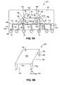
- FIG. 5Ais a cross-sectional side view of a semiconductor package including a support structure having a plurality of legs, according to one embodiment of the present invention.
- FIG. 5Bis a perspective view of the support structure of FIG. 5 A.
- FIG. 6Ais a cross-sectional side view of a semiconductor package including a leadframe support structure, according to one embodiment of the present invention.
- FIG. 6Bis a partially broken top plan view of the semiconductor package of FIG. 6 A.
- FIG. 7Ais a cross-sectional side view of a semiconductor package including a support structure having a circuit film disposed thereon, according to one embodiment of the present invention.
- FIGS. 7B, 7 C, and 7 Dare cross-sectional side views of alternate configurations of a circled portion of the semiconductor package shown in FIG. 7 A.
- FIG. 8is a cross-sectional side view of a semiconductor package including a support structure that functions as an electromagnetic interference (EMI) shield, according to one embodiment of the present invention.
- EMIelectromagnetic interference
- FIG. 9is a cross-sectional side view of a semiconductor package including a support structure having a die and a circuit element disposed on a circuit film that is on an inside surface of the support structure, according to one embodiment of the present invention.
- FIG. 10is a cross-sectional side view of a semiconductor package including a support structure having a flip chip die and a circuit element disposed on a circuit film that is on an inside surface of the support structure, according to one embodiment of the present invention.
- FIG. 11is a cross-sectional side view of a semiconductor package including a support structure that superimposes two dies, according to one embodiment of the present invention.
- FIG. 12Ais a cross-sectional side view of a semiconductor package including a heat spreader that is between and coupled to a pair of dies, according to one embodiment of the present invention.
- FIG. 12Bis a top plan view of the semiconductor package of FIG. 12 A.
- FIG. 13is a cross-sectional side view of a semiconductor package including a pair of dies and a pair of heat spreaders, according to one embodiment of the present invention.
- FIG. 14is a cross-sectional side view of a semiconductor package including a pair of dies and a pair of heat spreaders, according to one embodiment of the present invention.
- FIG. 15is a flow chart illustrating an exemplary semiconductor fabrication method, according to one embodiment of the present invention.
- FIG. 1is a cross-sectional view of a semiconductor package 2 - 1 including a support structure 14 , according to one embodiment of the present invention.
- Semiconductor package 2 - 1includes a rectangular substrate 10 having an upward-facing first surface 10 a and an opposite downward-facing second surface 10 b .
- a rectangular first die 12 having an upward-facing active first surface 12 a and an opposing downward-facing inactive second surface 12 bis mounted on a metal die pad 10 e of first surface 10 a .
- Die pad 10 emay be thermally coupled by a via 13 to a conductive ball 15 on second surface 10 b substrate 10 to transfer heat from first die 12 , and also may be electrically coupled (sometimes also stated as “electrically connected” herein) through those structures to an external reference voltage so as to provide the voltage to second surface 12 b of first die 12 .
- a free-standing support structure 14superimposes first die 12 and includes a vertically oriented first side 14 a , an opposite vertically oriented second side 14 b , and a horizontally oriented top side 14 c that is connected at right angles to first and second sides 14 a , 14 b .
- Topside 14 cincludes an upward-facing first surface 14 d and an opposite downward-facing second surface 14 e.
- support structure 14is generally rectangular in cross-section, but can have any shape. Typically, the corners are rounded, e.g., for ease of encapsulation.
- a rectangular second die 16 that is smaller in horizontal area than first die 12is mounted on first surface 14 d of top side 14 c .
- Second die 16has an upward-facing active first surface 16 a and an opposing downward-facing inactive second surface 16 b .
- Support structure 14can also have two additional vertically oriented sides (not visible in this cross-sectional view), and thus, may have a total of four vertically oriented sides.
- Support structure 14may include a plurality of horizontal feet 14 f as a base that rest on and are thermally coupled (e.g. by solder or a thermally conductive adhesive) to heat sinks accessible at first surface 10 a of substrate 10 .
- the heat sink of substrate 10may include metal or other thermally conductive regions 10 c on first surface 10 a that are thermally coupled to feet 14 f .
- Conductive regions 10 care thermally coupled by conductive vias 13 to conductive balls 15 on second surface 10 b of substrate 10 , or to an intermediate metal heat sink layer within substrate 10 (not shown).
- support structure 14may include pins 14 g that extend into precisely-located holes 10 d in first surface 10 a of substrate 10 for thermal coupling therein to vias 13 and conductive balls 15 .
- Substrate 10may include an insulative core layer with a layer of conductive first circuit patterns 11 a on first surface 10 a , and layer of conductive second circuit patterns 11 b on second surface 10 b .
- a layer of an insulative protective solder mask materialcovers portions of the circuit patterns 11 a , 11 b . While typically there will be many of the first and second circuit patterns 11 a , 11 b , only a few of them are shown in FIG. 1 for clarity of view.
- Respective first and second circuit patterns 11 a , 11 bare electrically interconnected by respective electrically conductive vias 13 that extend vertically through substrate 10 .
- the core layer of substrate 10may be composed of any type of package substrate material, such as glass fiber-filled epoxy laminate, ceramic, insulated metal, or polyimide.
- First and second circuit patterns 11 a and 11 b , die pad 10 f , conductive regions 10 c , and vias 13may be formed of patterned metal (e.g., copper).
- Interconnection balls 15may be fused to respective second circuit patterns 11 b to serve as input/output terminals for package 2 - 1 , and/or directly to the lower and of the vias 13 to conduct heat to an external motherboard.
- First surface 12 a of first die 12includes a plurality of peripheral input/output terminals, called bond pads 12 c herein, along two or four sides of first surface 12 a .
- bond pads 12 ccan be located at other portions of first surface 12 a , such as in the central portion of first surface 12 a .
- Bond pads 12 care electrically connected within support structure 14 to respective ones of the plurality of first circuit patterns 11 a on first surface 10 a of substrate 10 via conductive wires 18 .
- Second surface 12 b of first die 12can be affixed to die pad 10 e of first surface 10 a of substrate 10 using a thermally and/or electrically conductive adhesive.
- first die 12can be electrically connected to first circuit patterns 11 a in a flip-chip connection, thereby eliminating wires 18 .
- First surface 16 a of second die 16also includes a plurality of bond pads 16 c located near the perimeter of first surface 16 a along two or four sides of second die 16 . In other embodiments (not shown), bond pads 16 c can be located at other portions of first surface 15 a , such as in the central portion of first surface 15 a . Bond pads 16 c are electrically connected to circuit patterns 11 a that are located outside of support structure 14 via respective conductive wires 20 . Second surface 16 b of second die 16 is affixed to first surface 14 d of support structure 14 using a thermally conductive adhesive. In this embodiment, second die 16 is smaller in horizontal area than either first surface 14 d of support structure 14 or first die 12 .
- Support structure 14can be formed using many different materials.
- support structure 14is formed of a thermally conductive metal material, such as copper or aluminum.
- support structure 14is formed of a thermally conductive plastic or composite material.
- Support structure 14can be rigid or fairly rigid. With second die 16 thermally coupled to support structure 14 , support structure 14 provides a path to conduct heat from second die 16 to a heat sink of substrate 10 . Accordingly, package 2 - 1 has thermal advantages over conventional packages where a pair of dies are stacked one directly on the other, in which case heat from one of the stacked dies can flow into the other. In package 2 - 1 , heat from second die 16 is thermally conducted by support structure 14 to substrate 10 rather than to first die 12 .
- a protective insulative unitary body of a hardened encapsulant 19may be provided over first die 12 , conductive wires 18 , support structure 14 , second die 16 , conductive wires 20 , and all or a sub-portion of first surface 10 a of substrate 10 by molding or pouring a resin compound, such as epoxy, over substrate 10 .
- support structure 14includes one or more holes in its surfaces, e.g. through first or second sides 14 a , 14 b or top side 14 c , encapsulant 19 flows through the holes in support structure 14 during the encapsulation process, so as to cover first die 12 and conductive wires 18 with encapsulant 19 and fill the volume within support structure 14 with encapsulant 19 .
- a pre-formed protective cap or lidmade of metal or plastic can be mounted on first surface 10 a of substrate 10 and used to cover first die 12 , conductive wires 18 , support structure 14 , second die 16 , conductive wires 20 , and all or a sub-portion of first surface 10 a.
- first die 12 and conductive wires 18 with encapsulant 19 and filling the remaining volume within support structure 14 with encapsulant 19can be advantageous for at least the following reasons.
- encapsulant 19acts as a moisture barrier keeping moisture from contacting first die 12 and conductive wires 18 , as well as support structure 14 , second die 16 , conductive wires 20 , and a portion of first surface 10 a of substrate 10 .
- encapsulant 19increases the overall strength and physical integrity of semiconductor package 2 - 1 .
- encapsulant 19helps to ensure that semiconductor package 2 - 1 will not be damaged when exposed to different solder reflow temperatures.
- a support structure having no aperturesmay be provided to prevent the encapsulant from covering first die 12 .
- This type of support structuremay be hermetically sealed to first surface 10 a of substrate 10 such that an air pocket is formed within the support structure and is maintained even after the support structure itself is encapsulated.
- the substrate, support structure, encapsulant material, and assembly process/temperatureswould need to be selected so that unduly high pressures do not develop within the air pocket during the assembly process to avoid damaging (e.g., cracking) the semiconductor package.
- substrate 10may vary.
- package 2 - 1is shown as a ball grid array (BGA) package, but conductive balls 15 may be omitted so that package 2 - 1 is a land grid array (LGA) package.
- the example substrate 10includes a core insulative layer with layers of metal on the opposed surfaces thereof, substrate 10 is not limited to such a structure.
- substrate 10may be a thin film substrate or a rigid metal leadframe having a die pad and radiating metal leads.
- FIG. 2is a cross-sectional side view of a semiconductor package 2 - 2 , according to another embodiment of the present invention.
- Semiconductor package 2 - 2includes a metal support structure 14 that is electrically connected to at least one bond pad 16 c of second die 16 via a conductive metal wire 22 .
- wire 22can be electrically connected to a bond pad 16 c that is a ground terminal or some other reference voltage terminal of second die 16 .
- An opposite end of bond wire 22may be electrically connected to an exposed electrically conductive portion of first surface 14 d of top side 14 c of support structure 14 .
- Support structure 14may be electrically connected through conductive regions 10 c or a first circuit pattern 11 a on first surface 10 a of substrate 10 , a via 13 and a conductive ball 15 is to a ground or voltage source on a motherboard on which package 2 - 2 is mounted.
- support structure 14itself, or a conductive portion thereof, can be part of a conductive path that provides a ground or other reference voltage to a bond pad 16 c of second die 16 .
- an electrically conductive die attach pastecan be used to attach second surface 16 b of second die 16 to an electrically conductive portion of first surface 14 d of top side 14 c of support structure 14 to provide a ground or other reference voltage to the inactive second surface 16 b of second die 16 .
- FIG. 3shows a cross-sectional view of a semiconductor package 2 - 3 , according to another embodiment of the present invention.
- Semiconductor package 2 - 3includes a support structure 14 - 1 that has a recess 24 formed in a central portion of first surface 14 d of top side 14 c .
- Recess 24includes two downwardly sloping walls that taper into a central flat portion.
- Second die 16is disposed on the central flat portion of first surface 14 d within recess 24 .
- An advantage of this embodimentis that, by disposing second die 16 in recess 24 , the overall height H of semiconductor package 2 - 3 can be reduced by an amount equal to the depth of recess 24 .
- recess 24may be stamped into a metal support structure 14 - 1 .
- a recess 24may be provided in various other of the support structures discussed herein.
- FIG. 4shows a cross-sectional side view of a semiconductor package 2 - 4 , according to another embodiment of the present invention.
- Semiconductor package 2 - 4includes a support structure 14 that has a second die 16 with a relatively large horizontal area disposed on top side 14 c of support stricture 14 .
- the horizontal area of second die 16is greater than the horizontal area of first die 12 .
- An advantage of this embodimentis that it allows a large second die 16 to be stacked above a small first die 12 , while providing clearance for bond wires 18 and thermal protection for the pair of dies.
- FIG. 5Ais a side view of a semiconductor package 2 - 5 , including a support structure 14 - 2 , according to another embodiment of the present invention.
- FIG. 5Bis a perspective view of support structure 14 - 2 .
- Support structure 14 - 2has a vertical leg 14 g at each of the four corners of top side 14 c of support structure 14 - 2 .
- Each leghas a horizontally extending foot 14 f that is thermally coupled to conductive portion 10 c of substrate 10 .
- Opening 14 his between adjacent legs 14 g .
- Bond wires 18may be electrically connected between the bond pads 16 c of first die 12 and respective first circuit patterns 11 a on first surface 10 a of substrate 10 outside the perimeter of support structure 14 - 2 through openings 14 h between legs 14 g . Accordingly, the perimeter of support structure 14 - 2 and of package 2 - 5 may be smaller than that of support structure 14 and package 2 - 1 of FIG. 1, where bond wires 18 are entirely within support structure 14 .
- One or more of the feet 14 falso may be electrically connected to a reference voltage (e.g., ground) through a conductive ball 15 , via 13 , and conductive portion 10 c if it is desired to apply such a reference voltage to second surface 16 b of second die 16 .
- support structure 14 - 2is shown having four legs 14 g , it should be recognized support structure 14 - 2 can have any number of legs 14 g and openings 14 h arranged in any manner.
- Package 2 - 5's feature of having bond wires 18 that extend through openings 14 h of support structure 14 - 2 to a point of connection with first circuit patterns 11 a that is outside a perimeter of support structure 14 - 2 may be used with the other packages disclosed herein, such as, for example, package 2 - 3 and the packages discussed below.
- FIGS. 6A and 6Bare a cross-sectional side view and a partially broken top plan view, respectively, of a semiconductor package 2 - 6 , according to another embodiment of the present invention.
- Semiconductor package 2 - 6includes a metal support structure 14 - 3 that is patterned like a leadframe.
- support structure 14 - 3includes a rectangular metal central die pad 14 i supported by four metal tie bars 14 j that extend integrally from each of the four corners of die pad 14 i .
- a plurality of metal leads 14 kextend radially outward from each of the fours sides of die pad 14 i .
- Leads 14 k and tie bars 14 jare each bent downward at a steep angle or a right angle and then bent to form horizontal feet 14 m .
- Feet 14 m of leads 14 kare each electrically connected, e.g., by solder, to a first circuit pattern 11 a on first surface 10 a of substrate 10 .
- Bond wires 20electrically connect bond pads 16 c of second die 16 to respective leads 14 k .
- Layers of a non-conductive (e.g., polyimide) tape 14 n(shown by dashed lines in FIG.
- second die 16is electrically connected to first circuit pattern 11 a through leads 14 k .
- a voltage sourcee.g., ground
- second die 16may be mounted in a flip chip style on leads 14 k of support structure 14 - 3 .
- the bond pads 16 c of second die 16are superimposed over of leads 14 k , and are electrically connected thereto with solder or an electrically conductive adhesive.
- Die pad 14 imay or may not be present.
- second die 16may be mounted on the opposite, underside of die pad 14 i , so that second die 16 and bond wires 20 are entirely within support structure 14 - 3 .
- a circuit element 26optionally may be mounted on leads 14 k . Input/output terminals on circuit element 26 are electrically connected between a plurality of leads 14 k .
- Circuit element 26can be a passive circuit element, such as a resistor, a capacitor, or an inductor, or circuit element 26 can be an active circuit element, such as a semiconductor die.
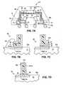
- FIG. 7Ais a cross-sectional side view of a semiconductor package 2 - 7 , according to another embodiment of the present invention.
- Semiconductor package 2 - 7includes a support structure 14 - 4 , which may be metal or a non-conductive material.
- a flexible circuit film 40is disposed on first surface 14 d of top side 14 c and outer sides 14 a , 14 b of support structure 14 - 4 .
- Circuit film 40may include, for instance, an insulative first layer 41 of polyimide that is attached using an adhesive layer to support structure 14 - 4 , and an overlying layer of conductive (e.g., metal) circuit traces 42 .
- Bond wires 20are used to electrically connect bond pads 16 c of second die 16 to conductive circuit traces 42 .
- FIGS. 7B, 7 C and 7 Dshow circled portion 50 of semiconductor package 2 - 7 in detail.
- FIGS. 7B, 7 C and 7 Dshow three different ways by which support structure 14 - 4 and circuit film 40 can be electrically and mechanically coupled to first surface 10 a of substrate 10 .
- support structure 14 - 4includes an outwardly bent foot 14 - 4 a over which first layer 41 and circuit traces 42 of circuit film 40 extend horizontally outward.
- Foot 14 - 4 a of support structure 14 - 4can be mechanically, electrically, and/or thermally coupled to juxtaposed conductive regions 10 c or circuit patterns 11 a of first surface 10 a of substrate 10 using any suitable means (e.g., by solder or a conductive adhesive).
- Conductive circuit traces 42are each electrically coupled to first circuit patterns 11 a of substrate 10 via one of a plurality of bond wires 46 .
- support structure 14 - 4includes an inwardly bent foot 14 - 4 b under which first layer 41 and circuit traces 42 of circuit film 40 extend horizontally inward. Bent portion 42 b of conductive circuit traces 42 can be mechanically, electrically, and/or thermally coupled to juxtaposed conductive regions 10 c or circuit patterns 11 a of first surface 10 a of substrate 10 using any suitable connection means 47 (e.g., by solder) disposed between them.
- connection means 47e.g., by solder
- support structure 14 - 4includes an end portion 14 - 4 c
- first layer 41includes an end portion 41 c
- conductive circuit traces 42include an end portion 42 c , all of which end in a common horizontal plane.
- End portion 41 c of support structure 14 - 4can be mechanically, electrically, and/or thermally coupled to juxtaposed conductive regions 10 c or circuit patterns 11 a of substrate 10 using any suitable means 48 (e.g., by solder or a conductive adhesive).
- end portion 42 c of circuit traces 42can be electrically coupled to circuit patterns 11 a of substrate 10 using any suitable means 49 (e.g., by solder or a conductive adhesive).
- circuit element 26may be disposed on circuit film 40 . Input/output terminals on circuit element 26 are electrically connected (e.g., soldered) between a plurality of circuit traces 42 .
- Circuit element 26can be a passive circuit element, such as a resistor, a capacitor, or an inductor, or circuit element 26 can be an active circuit element, such as a semiconductor die.
- second die 16is mounted in a flip-chip connection with circuit traces 42 of circuit film 40 . Bond pads 16 c of second die 16 are juxtaposed with and soldered to the circuit traces 42 .
- FIG. 8shows a cross-sectional side view of a semiconductor package 2 - 11 , according to another embodiment of the present invention.
- Semiconductor package 2 - 11includes a support structure 14 - 5 that functions as an electromagnetic interference (EMI) shield.
- Support structure 14 - 5is made of a material (e.g., metal) that is capable of shielding first die 12 from electromagnetic energy generated by second die 16 and other external electromagnetic energy sources.
- support structure 14 - 5may shield second die 16 from electromagnetic energy generated by first die 12 .
- Support structure 14 - 5can have a plurality of holes formed through it to allow encapsulant 19 to cover first die 12 , or support structure 14 - 5 can be solid with slots at its base to allow encapsulant 19 to fill the volume within support structure 14 - 5 .
- feet 14 f of support structure 14 - 5are electrically connected through conductive portion 10 c and a via 13 to an internal metal thermal and ground plane 10 f of substrate 10 , which in turn is electrically and thermally connected by another via 13 to one or more conductive balls 15 on second surface 10 b of substrate 10 .
- Other vias 13 that conduct signals to and from first die 12 and second die 16pass through apertures 10 h in thermal/ground plane 10 f.
- a bond pad 16 c and/or second side 16 b of second die 16may be electrically connected (by a bond wire 20 or a layer of an electrically conductive adhesive, respectively) to a conductive portion of support structure 14 , so that second die 16 may be electrically coupled to substrate layer 10 f through support structure 14 .
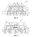
- FIG. 9shows a cross-sectional side view of a semiconductor package 2 - 9 , according to another embodiment of the present invention.
- Semiconductor package 2 - 9includes a support structure 14 - 6 that has a circuit film 40 and circuit traces 42 on its inside horizontal surface 14 e and inner sides 14 a , 14 b .
- Bond pads 16 c of second die 16are electrically connected via conductive wires 20 to circuit traces 42 .
- Circuit traces 42are electrically connected to first circuit patterns 11 a of substrate 10 , and from there to conductive balls 15 on second surface 10 b of substrate 10 .
- Optional circuit element 26may be mounted on circuit film 40 and electrically coupled across circuit traces 42 thereof.
- An advantage of this embodimentis that die 16 and circuit element 26 are both protected within support structure 14 .
- Support structure 14 - 6 and circuit film 40can be electrically, mechanically, and/or thermally coupled to first surface 10 a of substrate 10 in ways similar to those shown in FIGS. 7B, 7 C and 7 D.
- FIG. 10is a cross-sectional side view of a semiconductor package 2 - 10 , according to another embodiment of the present invention.
- Semiconductor package 2 - 10includes a support structure 14 - 6 , as in package 2 - 9 of FIG. 9, that has a second die 16 and a circuit element 26 mounted on circuit traces 42 of a circuit film 40 on inside surface 14 e of support structure 14 .
- Semiconductor package 2 - 10is similar to semiconductor package 2 - 9 , except that second die 16 is a flip-chip. Bond pads 16 c of second die 16 and circuit element 26 are electrically connected to circuit traces 42 of circuit film 40 by reflowed conductive balls.
- An adhesive insulative underfill material 44may be provided between first surface 16 a of second die 16 and circuit film 40 .
- Support structure 14 - 6 and circuit film 40can be electrically, mechanically, and/or thermally coupled to substrate 10 in ways similar to those shown in FIGS. 7B, 7 C and 7 D.
- FIG. 11is a cross-sectional side view of a semiconductor package 2 - 11 , according to another embodiment of the present invention.
- Semiconductor package 2 - 11includes a support structure 14 that superimposes both first die 12 and second die 16 .
- Inside second surface 14 e of top side 14 c of support structure 14is thermally coupled to inactive second surface 16 b of second die 16 via a thermal coupling means 30 .
- Coupling means 30can be an adhesive material that is thermally conductive and electrically insulative, such as a thermally conductive die attach paste or film.
- second die 16can be thermally coupled through support structure 14 to a heat sink of substrate 10 .
- coupling means 30can be a material that is thermally conductive and electrically conductive. In such an embodiment, where support structure 14 is also electrically conductive (e.g., is metal), a voltage can be applied to inactive second surface 16 b of second die 16 through support structure 14 .
- Second die 16is in a flip chip connection with first die 12 .
- bond pads 16 c on active first surface 16 a of second die 16are electrically connected by conductive balls 28 to corresponding centrally-located bond pads 12 c on active first surface 12 a of first die 12 .
- Peripheral bond pads 12 c of first die 12are electrically connected by bond wires 18 to first circuit patterns 11 a .
- An advantage of this embodimentis that support structure 14 provides a thermal path (and potentially a grounding path) from second die 16 to substrate 10 . Thus, heat generated by second die 16 will flow from second die 16 through support structure 14 into substrate 10 .
- FIGS. 12A and 12Bare a cross-sectional view and a top plan view, respectively, of a semiconductor package 2 - 12 , according to another embodiment of the present invention.
- Semiconductor package 2 - 12includes a lower first die 12 , a heat spreader 33 , and an upper second die 16 .
- Heat spreader 33can be made out of any material that has a high thermal conductivity. Such materials include copper, silver, aluminum, anodized aluminum, metal alloys, or carbon graphite. A metal heat spreader may be stamped from a thin flexible sheet of metal. Heat spreader 33 can have any shape and the shape of heat spreader 33 can be optimized so that encapsulant 19 flows smoothly through heat spreader 33 and covers first die 12 , thereby avoiding voids in encapsulant 19 .
- Active first surface 12 a of first die 12includes a plurality of bond pads 12 c that are respectively electrically coupled to first circuit patterns 11 a on first surface 10 a of substrate 10 by a plurality of conductive balls 28 in a flip-chip connection.
- First die 12 and its electrical connectionsare within a cavity defined by heat spreader 33 and first surface 10 a of substrate 10 .
- Active first surface 16 a of second die 16includes a plurality of bond pads 16 c that are respectively electrically coupled to a plurality of first circuit patterns 11 a on first surface 10 a of substrate 10 via a plurality of conductive wires 20 a and 20 b .
- First circuit patterns 11 aenable first die 12 and second die 16 to be electrically coupled to one another.
- Heat spreader 33has an upper first surface 33 a and an opposite lower second surface 33 b .
- Heat spreader 33is a unitary structure and includes a horizontally-extending peripheral base portion 33 c , a horizontal central upper portion 33 d , and an inclined vertical intermediate portion 33 e between base portion 33 c and upper portion 33 d .
- Base portion 33 cmay be thermally coupled, e.g., by solder or a thermally conductive adhesive, to a conductive portion 10 c at first surface 10 a of substrate 10 .
- Conductive portion 10 cmay be thermally coupled by vias 13 through substrate 10 to conductive balls 16 on second surface 10 b of substrate 10 .
- substrate 10may include an internal heat sink layer in a middle portion of substrate 10 , to which heat spreader 33 may be thermally coupled by conductive portions 10 c and vias 13 (see, e.g., FIG. 8 ).
- Thermal coupling means 30can be any type of thermally conductive material, such as a thermally conductive adhesive paste or a thermally conductive film-based die attach adhesive. Thermal coupling means 30 may also be electrically conductive, which would allow a reference voltage (e.g., ground) to be applied to second surfaces 12 b , 16 b through substrate 10 and heat spreader 33 .
- first and second dies 12 and 16may be thermally coupled through heat spreader 33 and substrate 10 to conductive balls 15 , which in turn can be fused to a heat sink of an external motherboard, thereby allowing heat to flow from first and second dies 12 and 16 to the motherboard.
- heat from first and second dies 12 and 16can be provided to an internal heat sink of substrate 10 .
- second die 16can be electrically connected to first circuit patterns 11 a on first surface 10 a of substrate 10 by conductive wires 20 a and/or conductive wires 20 b .
- Conductive wires 20 bare electrically connected to first circuit patterns 11 a beyond the outer ends of base portion 33 c of heat spreader 33 , i.e., between the perimeter of heat spreader 33 and the perimeter of substrate 10 .
- Conductive wires 20 aare electrically connected to first circuit patterns 11 a on first surface 10 a of substrate 10 through holes 17 provided in base portion 33 c of heat spreader 33 .
- the dimensions (i.e., W X and W Y ) of the semiconductor package 2 - 12can be reduced while still allowing many wires 20 a , 20 b bonds to be electrically connected to second die 16 .
- FIG. 13shows a cross-sectional view of a semiconductor package 2 - 13 , according to another embodiment of the present invention.
- Semiconductor package 2 - 13is similar to semiconductor package 2 - 12 of FIGS. 12A and 12B, except that package 2 - 13 includes a second heat spreader 35 .
- Heat spreader 35includes an upper first side 35 a , an opposite lower second side 35 b , a peripheral base portion 35 c , an upper central horizontal portion 35 d , and a vertically-inclined intermediate portion 35 e .
- Heat spreader 35is made of a highly thermally conductive material, e.g., a flexible stamped metal sheet, the same as described above for heat spreader 33 .
- Second surface 35 b of horizontal base portion 35 c of heat spreader 35is thermally coupled to first surface 33 a of base portion 33 c of heat spreader 33 , which in turn is thermally coupled to another conductive region 10 c of first surface 10 a of substrate 10 .
- Heat spreader 35is a means for further cooling of second die 16 .
- second surface 35 b of central horizontal portion 35 d of heat spreader 35is thermally coupled by an adhesive thermally conductive, electrically insulative coupling means 46 , e.g., a carbon-filled epoxy material, to active first surface 16 a of second die 16 .
- Central horizontal portion 35 dcontacts first surface 16 a within a perimeter defined by bond pads 16 c of second die 16 .
- Conductive wires 20are electrically connected to bond pads 16 c .
- Heat spreader 35has an apex portion 35 f which provides clearance for the apex of conductive wires 20 .
- Wires 20may be bonded-in a low loop height style.
- heat spreader 35superimposes the stack of first and second dies 12 and 16 and wires 20 .
- heat spreaders 33 and 35are provided with openings in intermediate portions 33 c and 35 e through which encapsulant 19 can penetrate to cover first and second dies 12 and 16 and fill the volumes within heat spreaders 33 , 35 .
- a third semiconductor diecan be electrically and thermally connected to first surface 35 a of central portion 35 d of heat spreader 35 over second die 16 using the various coupling means discussed above. It should also be recognized that a different number of heat spreaders and dies can be stacked (e.g., three heat spreaders and four dies) in accordance with the present invention.
- first die 12 of package 2 - 14is not flip chip bonded, but rather is inverted so that inactive second surface 12 b of first die 12 is thermally coupled to a die pad 10 e by a coupling means 30 , and bond pads 12 c are electrically coupled to first circuit patterns 11 a through bond wires 18 .
- first heat spreader 33is formed like second heat spreader 35 of FIG. 13 .
- an apex 33 fis provided in heat spreader 33 to provide clearance for low loop bond wires 18 , akin to apex 35 f of heat spreader 35 , and a horizontal central portion 33 d of first heat spreader 33 is thermally coupled between a central portion of first surface 12 a of first die 12 and second surface 16 b of second die 16 by a pair of thermal coupling means 30 .
- FIG. 15is a flow chart illustrating an exemplary semiconductor fabrication method 200 , according to one embodiment of the present invention.
- Method 200will be described in the context of semiconductor package 2 - 1 of FIG. 1 although it should be recognized that similar methods may be employed, with appropriate modifications, to make the other semiconductor packages described above.
- a substrate strip for making a plurality of packages 2 - 1is provided.
- the substrate stripincludes a single row or a two dimensional array of interconnected substrates 10 , which ultimately will be cut apart as a final assembly step.
- Each of the interconnected substratesincludes a die pad 10 e , first circuit patterns 11 a , vias 13 , second circuit patterns 11 b , and conductive regions 10 c , as described above.
- single substrates 10can be processed individually.
- Each single substrate 10can be carried in a substrate carrier, sometimes referred to as a “boat,” through the assembly process.
- a first die 12is mounted on the die pad 10 e of first surface 10 a of each of the substrates 10 of the substrate sheet.
- First die 12can be mounted on die pad 10 e , using any suitable technique such as by applying a thermally conductive adhesive to die pad 10 e , placing first die 12 onto the adhesive, and then curing the adhesive.
- step 206the bond pads 12 c of each first die 12 are each electrically connected to respective first circuit patterns 11 a of the respective substrate 10 .
- the electrical connectionsmay be made via conductive wires 18 (see FIG. 1 ).
- Conductive wires 18can be gold, copper, or aluminum wires, among other possibilities.
- a support structure 14is mounted on first surface 10 a of each substrate 10 over the first die 12 and in a thermal connection with a heat sink of substrate 10 .
- support structure 14may have horizontal feet 14 f that rest on first surface 10 a of substrate 10 , or support structure 14 can have pins 14 g that can be inserted into corresponding holes 10 d in first surface 10 a .
- Support structure 14can be thermally and, if desired, electrically coupled to one or plural conductive regions 10 c of first surface 10 a of substrate 10 using any suitable technique, such as by soldering or thermal adhesive attachment.
- a second die 16is mounted on first surface 14 d of top portion 14 c of the support structure 14 on each of the respective substrates 10 .
- Second die 16can be mounted on first surface 14 a of support structure 14 using any suitable technique, such as by applying a thermally conductive adhesive to first surface 14 a , placing second surface 16 b of the second die 16 on the adhesive, and then curing the adhesive. Alternatively, the thermal adhesive may be pre-applied to second die 16 .
- step 212the bond pads 16 c of each of the second dies 16 are each electrically connected to first circuit patterns 11 a on first surface 10 a of the respective substrate 10 .
- the electrical connectionsare made via conductive wires 20 , which may be, gold, copper or aluminum wires.
- a protective, insulative encapsulant 19is provided over each of the substrates 10 of strip 100 .
- the encapsulant 19covers second die 16 , wires 20 , support structure 14 , and all or part of first surface 10 a of substrate 10 . Since supports structure 14 has openings through it, encapsulant 19 also flows through the openings and covers first die 12 and conductive wires 18 and fills the volume within support structure 14 . Encapsulant 19 is thus vertically between first die 12 and second die 16 .
- Encapsulant 19may be, for example, an epoxy resin, and may be applied using molding or liquid encapsulation techniques.
- a separate cap of encapsulant 19may be provided over each substrate 10 of the substrate sheet, or a single block of encapsulant 19 may be provided over all of the substrates 10 of the substrate sheet, in which case the encapsulant is cut during a subsequent singulation step.
- step 216optional conductive balls 15 are fused onto a lower end of the vias 13 or onto second circuit patterns 11 b at second surface 10 b of the substrates 10 .
- conductive balls 15may be omitted, as in a land grid array package.
- Other conductive balls 15may be thermally coupled to the support structure 14 through a conductive region 10 c and a via 13 through substrate 10 , so that heat generated by second die 16 may be conducted through support structure 14 and substrate 10 to an external motherboard.
- step 218individual packages 2 - 1 are singulated from the substrate sheet using a punch, saw, laser, or the like, that severs the substrate strip into a plurality of semiconductor packages 2 - 1 .
- a snapable substrate sheetmay be used that snaps apart to singulate packages.
- the singulation stepmay cut through the encapsulant 19 as well as cutting through the substrate sheet, thereby forming orthogonal package sides (see, e.g., FIG. 1 ).
- a method of making package 2 - 2 of FIG. 2 and package 2 - 8 d of FIG. 8includes an additional step of electrically connecting support structure 14 to a conductive region 10 on first surface 10 a of substrate 10 so that a reference voltage may be provided to second die 16 through wire 22 .
- a method of making 2 - 4 of FIG. 4uses a larger second die 16 .
- Methods of making packages 2 - 3 and 2 - 5use a differently configured support structure, i.e., support structures 14 - 1 and 14 - 2 , respectively, as discussed above, but otherwise are similar to the method of making package 2 - 1 .
- Package 2 - 6 of FIGS. 6 and 7includes a metal support structure 14 - 3 that is patterned like a conventional leadframe, and has layers of an insulative tape to 14 n that interconnect and support leads 14 k and tie bars 14 j .
- second die 16may be electrically connected to the leads 14 k before or after leads 14 k are bend at right angles, and before or after support structure 14 - 3 is mounted on substrate 10 .
- Packages 2 - 7 and 2 - 9 of FIGS. 7 and 9, respectively,include a support structure 14 - 4 , 14 - 6 that includes a circuit film 40 attached to the support structure.
- the method of making the packageincludes additional steps of electrically connecting second die 16 to the respective circuit traces 42 of the circuit film 40 and mounting circuit element 26 (FIG. 9 A).
- a method of making package 2 - 10 of FIG. 10uses a flip chip style electrical connection for second die 16 , but is otherwise the same as the method of making package 2 - 9 .
- Second die 16is mounted before support structure 14 - 4 is mounted on substrate 10 .
- a method of making package 2 - 11 of FIG. 11requires a first die 12 with both central and peripheral bond pads 12 c on first surface 12 a .
- Second die 16is mounted on the central bond pads 12 c in a flip chip connection step, and the peripheral bond pads 12 c are connected by wires 18 to first circuit patterns 11 a before support structure 14 is mounted on substrate 11 .
- Coupling means 30is applied to second surface 16 b of second die 16 so that a thermal connection can be made between second surface 16 b and support structure 14 .
- a method of making packages 2 - 12 and 2 - 13 of FIGS. 12 and 13, respectively,includes electrically coupling first die 12 to first circuit patterns 11 a using a flip chip style connection. Further, a heat spreader 33 is provided rather than support structure 14 of FIG. 1 . Heat spreader 33 may be mounted on substrate 10 prior to or after mounting of second die 16 on heat spreader 33 . A heat spreader 35 subsequently may be attached to second die 16 , as in FIG. 13 .
- Package 2 - 14 of FIG. 14may be made by altering the above method of electrically connecting first die 12 to substrate 10 .
Landscapes
- Engineering & Computer Science (AREA)
- Microelectronics & Electronic Packaging (AREA)
- Physics & Mathematics (AREA)
- Power Engineering (AREA)
- Condensed Matter Physics & Semiconductors (AREA)
- General Physics & Mathematics (AREA)
- Computer Hardware Design (AREA)
- Health & Medical Sciences (AREA)
- Electromagnetism (AREA)
- Toxicology (AREA)
- Cooling Or The Like Of Semiconductors Or Solid State Devices (AREA)
- Structures Or Materials For Encapsulating Or Coating Semiconductor Devices Or Solid State Devices (AREA)
Abstract
Description
Claims (31)
Priority Applications (2)
| Application Number | Priority Date | Filing Date | Title |
|---|---|---|---|
| US10/013,396US6737750B1 (en) | 2001-12-07 | 2001-12-07 | Structures for improving heat dissipation in stacked semiconductor packages |
| US10/771,072US6919631B1 (en) | 2001-12-07 | 2004-02-02 | Structures for improving heat dissipation in stacked semiconductor packages |
Applications Claiming Priority (1)
| Application Number | Priority Date | Filing Date | Title |
|---|---|---|---|
| US10/013,396US6737750B1 (en) | 2001-12-07 | 2001-12-07 | Structures for improving heat dissipation in stacked semiconductor packages |
Related Child Applications (1)
| Application Number | Title | Priority Date | Filing Date |
|---|---|---|---|
| US10/771,072DivisionUS6919631B1 (en) | 2001-12-07 | 2004-02-02 | Structures for improving heat dissipation in stacked semiconductor packages |
Publications (1)
| Publication Number | Publication Date |
|---|---|
| US6737750B1true US6737750B1 (en) | 2004-05-18 |
Family
ID=32296364
Family Applications (2)
| Application Number | Title | Priority Date | Filing Date |
|---|---|---|---|
| US10/013,396Expired - LifetimeUS6737750B1 (en) | 2001-12-07 | 2001-12-07 | Structures for improving heat dissipation in stacked semiconductor packages |
| US10/771,072Expired - Fee RelatedUS6919631B1 (en) | 2001-12-07 | 2004-02-02 | Structures for improving heat dissipation in stacked semiconductor packages |
Family Applications After (1)
| Application Number | Title | Priority Date | Filing Date |
|---|---|---|---|
| US10/771,072Expired - Fee RelatedUS6919631B1 (en) | 2001-12-07 | 2004-02-02 | Structures for improving heat dissipation in stacked semiconductor packages |
Country Status (1)
| Country | Link |
|---|---|
| US (2) | US6737750B1 (en) |
Cited By (126)
| Publication number | Priority date | Publication date | Assignee | Title |
|---|---|---|---|---|
| US20030080414A1 (en)* | 2001-10-30 | 2003-05-01 | Kiss David A. | Packaged combination memory for electronic devices |
| US20030122246A1 (en)* | 2001-12-31 | 2003-07-03 | Mou-Shiung Lin | Integrated chip package structure using silicon substrate and method of manufacturing the same |
| US20030148597A1 (en)* | 2002-01-09 | 2003-08-07 | Tan Hock Chuan | Stacked die in die BGA package |
| US20030146509A1 (en)* | 2002-02-01 | 2003-08-07 | Broadcom Corporation | Ball grid array package with separated stiffener layer |
| US20030232486A1 (en)* | 2002-06-14 | 2003-12-18 | Shinko Electric Industries Co., Ltd. | Semiconductor device and method of manufacturing the same |
| US20040056277A1 (en)* | 2002-09-17 | 2004-03-25 | Chippac, Inc. | Semiconductor multi-package module including stacked-die package and having wire bond interconnect between stacked packages |
| US20040063246A1 (en)* | 2002-09-17 | 2004-04-01 | Chippac, Inc. | Semiconductor multi-package module having package stacked over die-down flip chip ball grid array package and having wire bond interconnect between stacked packages |
| US20040063242A1 (en)* | 2002-09-17 | 2004-04-01 | Chippac, Inc. | Semiconductor multi-package module having package stacked over ball grid array package and having wire bond interconnect between stacked packages |
| US20040061213A1 (en)* | 2002-09-17 | 2004-04-01 | Chippac, Inc. | Semiconductor multi-package module having package stacked over die-up flip chip ball grid array package and having wire bond interconnect between stacked packages |
| US20040061212A1 (en)* | 2002-09-17 | 2004-04-01 | Chippac, Inc. | Semiconductor multi-package module having wire bond interconnect between stacked packages |
| US20040065963A1 (en)* | 2002-09-17 | 2004-04-08 | Chippac, Inc. | Semiconductor multi-package module having wire bond interconnect between stacked packages and having electrical shield |
| US20040113253A1 (en)* | 2002-10-08 | 2004-06-17 | Chippac, Inc. | Semiconductor stacked multi-package module having inverted second package |
| US20040183180A1 (en)* | 2003-03-21 | 2004-09-23 | Advanced Semiconductor Engineering, Inc. | Multi-chips stacked package |
| US20040196635A1 (en)* | 2002-11-20 | 2004-10-07 | Hee-Jin Park | Stacked chip package with heat transfer wires |
| US20040198082A1 (en)* | 2003-04-07 | 2004-10-07 | Victor Zaderej | Method of making an electrical connector |
| US20040195591A1 (en)* | 2002-11-22 | 2004-10-07 | John Gehman | Digital and RF system and method therefor |
| US20040212056A1 (en)* | 2003-04-22 | 2004-10-28 | Kai-Chi Chen | [chip package structure] |
| US20040217485A1 (en)* | 2003-05-02 | 2004-11-04 | Advanced Semiconductor Engineering Inc. | Stacked flip chip package |
| US20040229418A1 (en)* | 2003-03-13 | 2004-11-18 | Seiko Epson Corporation | Electronic device and method of manufacturing the same, chip carrier, circuit board, and electronic instrument |
| US20040227238A1 (en)* | 2003-03-13 | 2004-11-18 | Seiko Epson Corporation | Electronic device and method of manufacturing the same, circuit board, and electronic instrument |
| US20050084715A1 (en)* | 2003-08-01 | 2005-04-21 | Hee Ching H. | Tilted media for hard disk drives and magnetic data storage devices |
| US20050104165A1 (en)* | 2002-05-22 | 2005-05-19 | Sharp Kabushiki Kaisha | Semiconductor element, semiconductor device, and method for manufacturing semiconductor element |
| US20050133916A1 (en)* | 2003-12-17 | 2005-06-23 | Stats Chippac, Inc | Multiple chip package module having inverted package stacked over die |
| US6919631B1 (en)* | 2001-12-07 | 2005-07-19 | Amkor Technology, Inc. | Structures for improving heat dissipation in stacked semiconductor packages |
| US20050230800A1 (en)* | 2004-04-16 | 2005-10-20 | St Assembly Test Services Ltd. | Thermally enhanced stacked die package and fabrication method |
| US20050280139A1 (en)* | 2004-06-21 | 2005-12-22 | Broadcom Corporation | Multipiece apparatus for thermal and electromagnetic interference (EMI) shielding enhancement in die-up array packages and method of making the same |
| US20050280127A1 (en)* | 2004-06-21 | 2005-12-22 | Broadcom Corporation | Apparatus and method for thermal and electromagnetic interference (EMI) shielding enhancement in die-up array packages |
| US20060003492A1 (en)* | 2002-08-30 | 2006-01-05 | Rajeev Joshi | Substrate based unmolded package |
| US20060007171A1 (en)* | 2004-06-24 | 2006-01-12 | Burdi Roger D | EMI resistant balanced touch sensor and method |
| US20060012018A1 (en)* | 2004-07-13 | 2006-01-19 | Chippac, Inc. | Semiconductor multipackage module including die and inverted land grid array package stacked over ball grid array package |
| WO2006016198A1 (en)* | 2004-08-02 | 2006-02-16 | Infineon Technologies Ag | Electronic component with stacked semiconductor chips and heat dissipating means |
| US20060038275A1 (en)* | 2004-08-11 | 2006-02-23 | Atsushi Yoshimura | Method and apparatus for manufacturing stacked-type semiconductor device |
| US20060051912A1 (en)* | 2004-09-09 | 2006-03-09 | Ati Technologies Inc. | Method and apparatus for a stacked die configuration |
| US20060071345A1 (en)* | 2004-09-30 | 2006-04-06 | Stmicroelectronics, Inc. | Copper interposer for reducing warping of integrated circuit packages and method of making IC packages |
| US20060091517A1 (en)* | 2004-10-29 | 2006-05-04 | Samsung Electro-Mechanics Co., Ltd. | Stacked semiconductor multi-chip package |
| US20060125042A1 (en)* | 2003-07-28 | 2006-06-15 | Edward Fuergut | Electronic component and panel for producing the same |
| US20060180916A1 (en)* | 2003-07-30 | 2006-08-17 | Koninklijke Philips Electronics N.V. | Ground arch for wirebond ball grid arrays |
| WO2006008679A3 (en)* | 2004-07-13 | 2006-08-24 | Koninkl Philips Electronics Nv | Electronic device comprising an integrated circuit |
| US20060192274A1 (en)* | 2004-11-12 | 2006-08-31 | Chippac, Inc | Semiconductor package having double layer leadframe |
| US20060220209A1 (en)* | 2005-03-31 | 2006-10-05 | Stats Chippac Ltd. | Semiconductor stacked package assembly having exposed substrate surfaces on upper and lower sides |
| US20060220210A1 (en)* | 2005-03-31 | 2006-10-05 | Stats Chippac Ltd. | Semiconductor assembly including chip scale package and second substrate and having exposed substrate surfaces on upper and lower sides |
| US20060237829A1 (en)* | 2005-04-26 | 2006-10-26 | Eiichi Hosomi | Method and system for a semiconductor package with an air vent |
| US20060238961A1 (en)* | 2005-03-29 | 2006-10-26 | Atsushi Saita | Circuit device |
| US20060244117A1 (en)* | 2005-04-29 | 2006-11-02 | Stats Chippac, Ltd. | Semiconductor package including second substrate and having exposed substrate surfaces on upper and lower sides |
| US20060246624A1 (en)* | 2003-11-11 | 2006-11-02 | Edward Fuergut | Semiconductor device with semiconductor chip and rewiring layer and method for producing the same |
| US20060249851A1 (en)* | 2005-05-05 | 2006-11-09 | Stats Chippac Ltd. | Multiple Chip Package Module Including Die Stacked Over Encapsulated Package |
| US20060284299A1 (en)* | 2005-06-20 | 2006-12-21 | Stats Chippac Ltd. | Module Having Stacked Chip Scale Semiconductor Packages |
| US20070018296A1 (en)* | 2004-05-24 | 2007-01-25 | Chippac, Inc | Stacked Semiconductor Package having Adhesive/Spacer Structure and Insulation |
| US20070090502A1 (en)* | 2005-10-20 | 2007-04-26 | Broadcom Corporation | Methods and apparatus for improved thermal performance and electromagnetic interference (EMI) shielding in leadframe integrated circuit (IC) packages |
| US20070108595A1 (en)* | 2005-11-16 | 2007-05-17 | Ati Technologies Inc. | Semiconductor device with integrated heat spreader |
| US20070108562A1 (en)* | 2001-07-10 | 2007-05-17 | Samsung Electronics Co., Ltd. | Semiconductor chip having bond pads |
| US20070109756A1 (en)* | 2005-02-10 | 2007-05-17 | Stats Chippac Ltd. | Stacked integrated circuits package system |
| US20070134599A1 (en)* | 2005-12-14 | 2007-06-14 | Intel Corporation | In-situ functionalization of carbon nanotubes |
| US20070158815A1 (en)* | 2004-04-02 | 2007-07-12 | Chen Fung L | Multi-chip ball grid array package and method of manufacture |
| US20070164446A1 (en)* | 2006-01-13 | 2007-07-19 | Hawk Donald E Jr | Integrated circuit having second substrate to facilitate core power and ground distribution |
| US20070176281A1 (en)* | 2006-01-27 | 2007-08-02 | Advanced Semiconductor Engineering, Inc. | Semiconductor package |
| US20070235846A1 (en)* | 2006-04-01 | 2007-10-11 | Stats Chippac Ltd. | Integrated circuit package system with net spacer |
| US20070267734A1 (en)* | 2006-05-16 | 2007-11-22 | Broadcom Corporation | No-lead IC packages having integrated heat spreader for electromagnetic interference (EMI) shielding and thermal enhancement |
| US20070274058A1 (en)* | 2004-04-16 | 2007-11-29 | Koninklijke Philips Electronic N.V. | Integrated Circuit, a Method and an Assembly for Manufacturing the Integrated Circuit, and a Mobile Phone Having the Integrated Circuit |
| US20070273049A1 (en)* | 2006-05-12 | 2007-11-29 | Broadcom Corporation | Interconnect structure and formation for package stacking of molded plastic area array package |
| US20080029869A1 (en)* | 2006-08-01 | 2008-02-07 | Samsung Electronics Co., Ltd. | Vertical stack type multi-chip package having improved grounding performance and lower semiconductor chip reliability |
| US20080073756A1 (en)* | 2006-09-22 | 2008-03-27 | Infineon Technologies Ag | Module with a shielding and/or heat dissipating element |
| US20080169549A1 (en)* | 2005-04-29 | 2008-07-17 | Flynn Carson | Stacked integrated circuit package system and method of manufacture therefor |
| US20080179729A1 (en)* | 2005-03-31 | 2008-07-31 | Il Kwon Shim | Encapsulant cavity integrated circuit package system |
| US20080197477A1 (en)* | 2006-08-31 | 2008-08-21 | Ati Technologies Inc. | Flip-Chip Grid Ball Array Strip and Package |
| US20080197468A1 (en)* | 2007-02-15 | 2008-08-21 | Advanced Semiconductor Engineering, Inc. | Package structure and manufacturing method thereof |
| US20080211089A1 (en)* | 2007-02-16 | 2008-09-04 | Broadcom Corporation | Interposer for die stacking in semiconductor packages and the method of making the same |
| US20080217765A1 (en)* | 2007-03-02 | 2008-09-11 | Yoder Jay A | Semiconductor component and method of manufacture |
| US20080277770A1 (en)* | 2007-04-27 | 2008-11-13 | Kabushiki Kaisha Toshiba | Semiconductor device |
| US20080290502A1 (en)* | 2007-05-25 | 2008-11-27 | Zafer Kutlu | Integrated circuit package with soldered lid for improved thermal performance |
| US20080303124A1 (en)* | 2007-06-08 | 2008-12-11 | Broadcom Corporation | Lead frame-BGA package with enhanced thermal performance and I/O counts |
| US20090039523A1 (en)* | 2007-08-07 | 2009-02-12 | Tongbi Jiang | Packaged integrated circuit devices with through-body conductive vias, and methods of making same |
| US20090065911A1 (en)* | 2007-09-12 | 2009-03-12 | Advanced Semiconductor Engineering, Inc. | Semiconductor package and manufacturing method thereof |
| US20090079065A1 (en)* | 2007-09-21 | 2009-03-26 | Infineon Technologies Ag | Semiconductor device including electronic component coupled to a backside of a chip |
| US20090079061A1 (en)* | 2003-03-05 | 2009-03-26 | Debendra Mallik | Thermally enhanced electronic flip-chip packaging with external-connector-side die and method |
| US20090194853A1 (en)* | 2006-12-22 | 2009-08-06 | Ki Youn Jang | Shielded stacked integrated circuit packaging system and method of manufacture thereof |
| US20090194882A1 (en)* | 2008-02-06 | 2009-08-06 | Infineon Technologies Ag | Electronic device |
| US20100014251A1 (en)* | 2008-07-15 | 2010-01-21 | Advanced Micro Devices, Inc. | Multidimensional Thermal Management Device for an Integrated Circuit Chip |
| US7652376B2 (en) | 2006-01-04 | 2010-01-26 | Stats Chippac Ltd. | Integrated circuit package system including stacked die |
| US7749807B2 (en) | 2003-04-04 | 2010-07-06 | Chippac, Inc. | Method of fabricating a semiconductor multipackage module including a processor and memory package assemblies |
| US7750482B2 (en) | 2006-02-09 | 2010-07-06 | Stats Chippac Ltd. | Integrated circuit package system including zero fillet resin |
| US7768125B2 (en) | 2006-01-04 | 2010-08-03 | Stats Chippac Ltd. | Multi-chip package system |
| US20100230822A1 (en)* | 2009-03-13 | 2010-09-16 | Stats Chippac, Ltd. | Semiconductor Die and Method of Forming Noise Absorbing Regions Between THVS in Peripheral Region of the Die |
| US7808087B2 (en) | 2006-06-01 | 2010-10-05 | Broadcom Corporation | Leadframe IC packages having top and bottom integrated heat spreaders |
| US20100258928A1 (en)* | 2009-04-14 | 2010-10-14 | Chi Heejo | Integrated circuit packaging system with stacked integrated circuit and method of manufacture thereof |
| US20100283151A1 (en)* | 2003-03-11 | 2010-11-11 | Micron Technology, Inc. | Techniques for packaging multiple device components |
| US20110068459A1 (en)* | 2009-09-23 | 2011-03-24 | Stats Chippac, Ltd. | Semiconductor Device and Method of Forming Interposer with Opening to Contain Semiconductor Die |
| US20110210442A1 (en)* | 2008-11-07 | 2011-09-01 | Shoa Siong Lim | Semiconductor Package and Trace Substrate with Enhanced Routing Design Flexibility and Method of Manufacturing Thereof |
| US8084868B1 (en)* | 2008-04-17 | 2011-12-27 | Amkor Technology, Inc. | Semiconductor package with fast power-up cycle and method of making same |
| WO2012020064A1 (en)* | 2010-08-10 | 2012-02-16 | St-Ericsson Sa | Packaging an integrated circuit die |
| US8129824B1 (en)* | 2008-12-03 | 2012-03-06 | Amkor Technology, Inc. | Shielding for a semiconductor package |
| US20120131794A1 (en)* | 2002-04-11 | 2012-05-31 | Greenberg Robert J | Biocompatible Bonding Method and Electronics Package Suitable for Implantation |
| US20120139097A1 (en)* | 2010-12-02 | 2012-06-07 | Jeonggi Jin | Semiconductor package and method of manufacturing the same |
| US20120146243A1 (en)* | 2007-09-21 | 2012-06-14 | Sungmin Song | Integrated circuit packaging system with interposer |
| US20120168916A1 (en)* | 2009-09-23 | 2012-07-05 | Stats Chippac, Ltd. | Semiconductor Device and Method of Forming Open Cavity in TSV Interposer to Contain Semiconductor Die in WLCSMP |
| US20120241935A1 (en)* | 2011-03-24 | 2012-09-27 | Chipmos Technologies Inc. | Package-on-package structure |
| CN103050467A (en)* | 2011-10-14 | 2013-04-17 | 乾坤科技股份有限公司 | Package structure and method for manufacturing the same |
| US8552551B2 (en) | 2004-05-24 | 2013-10-08 | Chippac, Inc. | Adhesive/spacer island structure for stacking over wire bonded die |
| US8581381B2 (en) | 2006-06-20 | 2013-11-12 | Broadcom Corporation | Integrated circuit (IC) package stacking and IC packages formed by same |
| US20130320513A1 (en)* | 2012-06-04 | 2013-12-05 | Siliconware Precision Industries Co., Ltd. | Semiconductor package and fabrication method thereof |
| US8623704B2 (en) | 2004-05-24 | 2014-01-07 | Chippac, Inc. | Adhesive/spacer island structure for multiple die package |
| US20140084446A1 (en)* | 2012-09-24 | 2014-03-27 | Soojeoung PARK | Semiconductor package and semiconductor devices with the same |
| US8704349B2 (en) | 2006-02-14 | 2014-04-22 | Stats Chippac Ltd. | Integrated circuit package system with exposed interconnects |
| CN103915418A (en)* | 2013-01-08 | 2014-07-09 | 矽品精密工业股份有限公司 | Semiconductor package and fabrication method thereof |
| US20140252581A1 (en)* | 2013-03-05 | 2014-09-11 | Mariano Layson Ching, Jr. | Lead frame and substrate semiconductor package |
| US8835221B2 (en) | 2001-12-31 | 2014-09-16 | Qualcomm Incorporated | Integrated chip package structure using ceramic substrate and method of manufacturing the same |
| US20140335655A1 (en)* | 2008-09-27 | 2014-11-13 | Rui Huang | Integrated circuit package system with mounting structure |
| US20140374891A1 (en)* | 2013-06-24 | 2014-12-25 | Boon Yew Low | Semiconductor device with heat spreader and thermal sheet |
| US20150014852A1 (en)* | 2013-07-12 | 2015-01-15 | Yueli Liu | Package assembly configurations for multiple dies and associated techniques |
| US20150014862A1 (en)* | 2013-07-11 | 2015-01-15 | Heungkyu Kwon | Semiconductor packages including a metal layer between first and second semiconductor chips |
| US9054013B2 (en)* | 2011-06-09 | 2015-06-09 | Optiz, Inc. | Method of making 3D integration microelectronic assembly for integrated circuit devices |
| US20150262904A1 (en)* | 2014-03-14 | 2015-09-17 | Taiwan Semiconductor Manufacturing Company, Ltd. | Package with Embedded Heat Dissipation Features |
| US20170025388A1 (en)* | 2015-07-22 | 2017-01-26 | Microchip Technology Incorporated | Backside Stacked Die In An Integrated Circuit (IC) Package |
| US9887145B2 (en)* | 2015-04-03 | 2018-02-06 | Dawning Leading Technology Inc. | Metal top stacking package structure and method for manufacturing the same |
| CN110444525A (en)* | 2018-05-02 | 2019-11-12 | 半导体元件工业有限责任公司 | The packaging part of semiconductor power device and the method for encapsulating semiconductor power device |
| US20200395300A1 (en)* | 2019-06-13 | 2020-12-17 | Intel Corporation | Substrateless double-sided embedded multi-die interconnect bridge |
| CN112201653A (en)* | 2019-07-08 | 2021-01-08 | 安靠科技新加坡控股私人有限公司 | Semiconductor device and method of manufacturing semiconductor device |
| CN112908984A (en)* | 2021-01-18 | 2021-06-04 | 上海先方半导体有限公司 | SSD (solid State disk) stacked packaging structure with radiating fins and manufacturing method thereof |
| US11227821B2 (en) | 2020-04-21 | 2022-01-18 | Toyota Motor Engineering & Manufacturing North America, Inc. | Chip-on-chip power card with embedded thermal conductor |
| CN114496813A (en)* | 2022-01-24 | 2022-05-13 | 西安微电子技术研究所 | A method of stacking bare chips |
| GB2603920A (en)* | 2021-02-18 | 2022-08-24 | Zhuzhou Crrc Times Electric Uk Innovation Center | Power Semiconductor Package |
| CN115527961A (en)* | 2022-10-19 | 2022-12-27 | 广东省科学院半导体研究所 | Multi-chip interconnection packaging structure with heat dissipation plate and preparation method thereof |
| US20230022159A1 (en)* | 2021-07-15 | 2023-01-26 | Kioxia Corporation | Semiconductor device and semiconductor device manufacturing method |
| US20230104397A1 (en)* | 2021-10-01 | 2023-04-06 | Advanced Semiconductor Engineering, Inc. | Semiconductor package shielding structure |
| US12293955B2 (en) | 2018-05-02 | 2025-05-06 | Semiconductor Components Industries, Llc | High power module package structures |
| CN120319734A (en)* | 2025-06-16 | 2025-07-15 | 甬矽电子(宁波)股份有限公司 | Flip chip ball grid array heat sink structure and preparation method thereof |
Families Citing this family (50)
| Publication number | Priority date | Publication date | Assignee | Title |
|---|---|---|---|---|
| JP4538830B2 (en)* | 2004-03-30 | 2010-09-08 | ルネサスエレクトロニクス株式会社 | Semiconductor device |
| TWI239611B (en)* | 2004-04-19 | 2005-09-11 | Advanced Semiconductor Eng | Multi chip module with embedded package configuration and method for manufacturing the same |
| TWI237882B (en)* | 2004-05-11 | 2005-08-11 | Via Tech Inc | Stacked multi-chip package |
| US7245003B2 (en)* | 2004-06-30 | 2007-07-17 | Intel Corporation | Stacked package electronic device |
| TWI250592B (en)* | 2004-11-16 | 2006-03-01 | Siliconware Precision Industries Co Ltd | Multi-chip semiconductor package and fabrication method thereof |
| KR100639701B1 (en)* | 2004-11-17 | 2006-10-30 | 삼성전자주식회사 | Multichip Package |
| US7528474B2 (en)* | 2005-05-31 | 2009-05-05 | Stats Chippac Ltd. | Stacked semiconductor package assembly having hollowed substrate |
| US20070108583A1 (en)* | 2005-08-08 | 2007-05-17 | Stats Chippac Ltd. | Integrated circuit package-on-package stacking system |
| US8643163B2 (en)* | 2005-08-08 | 2014-02-04 | Stats Chippac Ltd. | Integrated circuit package-on-package stacking system and method of manufacture thereof |
| TWI292617B (en)* | 2006-02-03 | 2008-01-11 | Siliconware Precision Industries Co Ltd | Stacked semiconductor structure and fabrication method thereof |
| US8810018B2 (en)* | 2006-02-03 | 2014-08-19 | Stats Chippac Ltd. | Stacked integrated circuit package system with face to face stack configuration |
| US8373195B2 (en) | 2006-04-12 | 2013-02-12 | SemiLEDs Optoelectronics Co., Ltd. | Light-emitting diode lamp with low thermal resistance |
| US7863639B2 (en)* | 2006-04-12 | 2011-01-04 | Semileds Optoelectronics Co. Ltd. | Light-emitting diode lamp with low thermal resistance |
| DE102006032073B4 (en)* | 2006-07-11 | 2016-07-07 | Intel Deutschland Gmbh | Electrically conductive composite of a component and a carrier plate |
| US7420206B2 (en)* | 2006-07-12 | 2008-09-02 | Genusion Inc. | Interposer, semiconductor chip mounted sub-board, and semiconductor package |
| KR20080022452A (en)* | 2006-09-06 | 2008-03-11 | 삼성전자주식회사 | PPO package and its manufacturing method |
| US7906844B2 (en)* | 2006-09-26 | 2011-03-15 | Compass Technology Co. Ltd. | Multiple integrated circuit die package with thermal performance |
| TWI334215B (en)* | 2007-01-26 | 2010-12-01 | Advanced Semiconductor Eng | Semiconductor package having electromagnetic shielding cap |
| KR101413220B1 (en)* | 2007-10-02 | 2014-06-30 | 삼성전자주식회사 | Semiconductor package having interposer and method for manufacturing semiconductor package |
| US8178956B2 (en)* | 2007-12-13 | 2012-05-15 | Stats Chippac Ltd. | Integrated circuit package system for shielding electromagnetic interference |
| US7687920B2 (en)* | 2008-04-11 | 2010-03-30 | Stats Chippac Ltd. | Integrated circuit package-on-package system with central bond wires |
| US7956449B2 (en)* | 2008-06-25 | 2011-06-07 | Stats Chippac Ltd. | Stacked integrated circuit package system |
| US7705447B2 (en)* | 2008-09-29 | 2010-04-27 | Intel Corporation | Input/output package architectures, and methods of using same |
| US8184440B2 (en)* | 2009-05-01 | 2012-05-22 | Abl Ip Holding Llc | Electronic apparatus having an encapsulating layer within and outside of a molded frame overlying a connection arrangement on a circuit board |
| US8786063B2 (en)* | 2009-05-15 | 2014-07-22 | Stats Chippac Ltd. | Integrated circuit packaging system with leads and transposer and method of manufacture thereof |
| JP2011077108A (en)* | 2009-09-29 | 2011-04-14 | Elpida Memory Inc | Semiconductor device |
| US8404518B2 (en)* | 2009-12-13 | 2013-03-26 | Stats Chippac Ltd. | Integrated circuit packaging system with package stacking and method of manufacture thereof |
| JP5633210B2 (en) | 2010-06-28 | 2014-12-03 | 富士通セミコンダクター株式会社 | Semiconductor device |
| US8516831B2 (en) | 2010-07-01 | 2013-08-27 | Toyota Motor Engineering & Manufacturing North America, Inc. | Thermal energy steering device |
| KR20120053332A (en)* | 2010-11-17 | 2012-05-25 | 삼성전자주식회사 | Semiconductor package and method of forming the same |
| US8351221B2 (en)* | 2011-01-14 | 2013-01-08 | Rf Micro Devices, Inc. | Stacked shield compartments for electronic components |
| TWI451543B (en)* | 2011-03-07 | 2014-09-01 | Unimicron Technology Corp | Package structure and its manufacturing method and package stacking device |
| DE102011109006A1 (en)* | 2011-07-29 | 2013-01-31 | Epcos Ag | Housing for a semiconductor chip and semiconductor chip with a housing |
| US10163744B2 (en)* | 2011-09-07 | 2018-12-25 | STATS ChipPAC Pte. Ltd. | Semiconductor device and method of forming a low profile dual-purpose shield and heat-dissipation structure |
| US8736046B2 (en)* | 2011-10-18 | 2014-05-27 | Stmicroelectronics Asia Pacific Pte Ltd. | Dual interlock heatsink assembly for enhanced cavity PBGA packages, and method of manufacture |
| ITMI20120711A1 (en) | 2012-04-27 | 2013-10-28 | St Microelectronics Srl | POWER DEVICE |
| ITMI20120713A1 (en) | 2012-04-27 | 2013-10-28 | St Microelectronics Srl | ELECTRONIC ASSEMBLY SYSTEM THROUGH THROUGH HOLES WITH DISSIPATED ELEMENTS CLOSED AMONG THEM AGAINST INSULATING BODY |
| ITMI20120712A1 (en)* | 2012-04-27 | 2013-10-28 | St Microelectronics Srl | ELECTRONIC LOOP-MOUNTED DEVICE WITH DOUBLE HEAT SINK |
| US8569870B1 (en) | 2012-06-25 | 2013-10-29 | Stats Chippac Ltd. | Integrated circuit packaging system with shielding spacer and method of manufacture thereof |
| CN103762208B (en)* | 2014-01-28 | 2016-08-10 | 扬智科技股份有限公司 | semiconductor structure |
| KR102228461B1 (en)* | 2014-04-30 | 2021-03-17 | 삼성전자주식회사 | Semiconductor Package Device |
| JP6438225B2 (en)* | 2014-07-24 | 2018-12-12 | 株式会社ジェイデバイス | Semiconductor package |
| TWI747805B (en)* | 2014-10-08 | 2021-12-01 | 日商索尼半導體解決方案公司 | Imaging device, manufacturing method, and electronic equipment |
| US9728510B2 (en) | 2015-04-10 | 2017-08-08 | Analog Devices, Inc. | Cavity package with composite substrate |
| KR102372300B1 (en)* | 2015-11-26 | 2022-03-08 | 삼성전자주식회사 | Stacked package and method of manufacturing the same |
| KR101734712B1 (en)* | 2015-12-09 | 2017-05-11 | 현대자동차주식회사 | Power module |
| US10192843B1 (en) | 2017-07-26 | 2019-01-29 | Micron Technology, Inc. | Methods of making semiconductor device modules with increased yield |
| US10410971B2 (en)* | 2017-08-29 | 2019-09-10 | Qualcomm Incorporated | Thermal and electromagnetic interference shielding for die embedded in package substrate |
| US11011447B2 (en)* | 2018-08-14 | 2021-05-18 | Taiwan Semiconductor Manufacturing Co., Ltd. | Semiconductor package and method for forming the same |
| US11621245B2 (en) | 2020-06-03 | 2023-04-04 | Micron Technology, Inc. | Microelectronic device packages with EMI shielding, methods of fabricating and related electronic systems |
Citations (53)
| Publication number | Priority date | Publication date | Assignee | Title |
|---|---|---|---|---|
| JPS5662351A (en) | 1979-10-26 | 1981-05-28 | Hitachi Ltd | Semiconductor device for memory |
| JPS60182731A (en) | 1984-02-29 | 1985-09-18 | Toshiba Corp | Semiconductor device |
| JPS61117858A (en) | 1984-11-14 | 1986-06-05 | Hitachi Micro Comput Eng Ltd | Semiconductor device |
| JPS62126661A (en) | 1985-11-27 | 1987-06-08 | Nec Corp | Hybrid integrated circuit device |
| JPS63128736A (en) | 1986-11-19 | 1988-06-01 | Olympus Optical Co Ltd | Semiconductor element |
| US4763188A (en) | 1986-08-08 | 1988-08-09 | Thomas Johnson | Packaging system for multiple semiconductor devices |
| JPS63244654A (en) | 1987-03-31 | 1988-10-12 | Toshiba Corp | Resin-encapsulated integrated circuit device |
| JPS641269A (en) | 1987-06-24 | 1989-01-05 | Hitachi Ltd | Semiconductor device |
| JPS6428856A (en) | 1987-07-23 | 1989-01-31 | Mitsubishi Electric Corp | Multilayered integrated circuit |
| JPS6471162A (en) | 1987-09-11 | 1989-03-16 | Hitachi Ltd | Semiconductor device |
| JPH0199248A (en) | 1987-10-13 | 1989-04-18 | Mitsubishi Electric Corp | semiconductor equipment |
| US5012323A (en) | 1989-11-20 | 1991-04-30 | Micron Technology, Inc. | Double-die semiconductor package having a back-bonded die and a face-bonded die interconnected on a single leadframe |
| US5025306A (en) | 1988-08-09 | 1991-06-18 | Texas Instruments Incorporated | Assembly of semiconductor chips |
| JPH03169062A (en) | 1989-11-28 | 1991-07-22 | Nec Kyushu Ltd | Semiconductor device |
| JPH0428260A (en) | 1990-05-23 | 1992-01-30 | Matsushita Electric Ind Co Ltd | Method of mounting semiconductor chip |
| JPH0456262A (en) | 1990-06-25 | 1992-02-24 | Matsushita Electron Corp | Semiconductor integrated circuit device |
| JPH0496358A (en) | 1990-08-13 | 1992-03-27 | Casio Comput Co Ltd | Printed wiring board |
| JPH04116859A (en) | 1990-09-06 | 1992-04-17 | Mitsubishi Electric Corp | semiconductor equipment |
| EP0503201A2 (en) | 1990-12-20 | 1992-09-16 | Kabushiki Kaisha Toshiba | Semiconductor device having an interconnecting circuit board and method for manufacturing same |
| US5166772A (en) | 1991-02-22 | 1992-11-24 | Motorola, Inc. | Transfer molded semiconductor device package with integral shield |
| JPH0513665A (en) | 1991-06-28 | 1993-01-22 | Nec Corp | Method for mounting tab chip |
| JPH0575015A (en) | 1991-09-13 | 1993-03-26 | Sharp Corp | Semiconductor device |
| US5200809A (en) | 1991-09-27 | 1993-04-06 | Vlsi Technology, Inc. | Exposed die-attach heatsink package |
| JPH05109975A (en) | 1991-10-14 | 1993-04-30 | Hitachi Ltd | Resin-sealed type semiconductor device |
| JPH05136323A (en) | 1991-11-13 | 1993-06-01 | Nec Corp | Integrated circuit device |
| US5291061A (en) | 1993-04-06 | 1994-03-01 | Micron Semiconductor, Inc. | Multi-chip stacked devices |
| US5323060A (en) | 1993-06-02 | 1994-06-21 | Micron Semiconductor, Inc. | Multichip module having a stacked chip arrangement |
| US5347429A (en) | 1990-11-14 | 1994-09-13 | Hitachi, Ltd. | Plastic-molded-type semiconductor device |
| US5365107A (en) | 1992-06-04 | 1994-11-15 | Shinko Electric Industries, Co., Ltd. | Semiconductor device having tab tape |
| US5422435A (en) | 1992-05-22 | 1995-06-06 | National Semiconductor Corporation | Stacked multi-chip modules and method of manufacturing |
| US5463253A (en) | 1990-03-15 | 1995-10-31 | Fujitsu Limited | Semiconductor device having a plurality of chips |
| US5530202A (en) | 1995-01-09 | 1996-06-25 | At&T Corp. | Metallic RF or thermal shield for automatic vacuum placement |
| US5656864A (en) | 1993-09-09 | 1997-08-12 | Fujitsu Limited | Semiconductor device having upper and lower package bodies and manufacturing method thereof |
| US5689135A (en) | 1995-12-19 | 1997-11-18 | Micron Technology, Inc. | Multi-chip device and method of fabrication employing leads over and under processes |
| US5696031A (en) | 1996-11-20 | 1997-12-09 | Micron Technology, Inc. | Device and method for stacking wire-bonded integrated circuit dice on flip-chip bonded integrated circuit dice |
| US5721452A (en) | 1995-08-16 | 1998-02-24 | Micron Technology, Inc. | Angularly offset stacked die multichip device and method of manufacture |
| US5739581A (en) | 1995-11-17 | 1998-04-14 | National Semiconductor Corporation | High density integrated circuit package assembly with a heatsink between stacked dies |
| US5793108A (en) | 1995-05-30 | 1998-08-11 | Sharp Kabushiki Kaisha | Semiconductor integrated circuit having a plurality of semiconductor chips |
| JPH10256470A (en) | 1997-03-10 | 1998-09-25 | Sanyo Electric Co Ltd | Semiconductor device |
| US5815372A (en) | 1997-03-25 | 1998-09-29 | Intel Corporation | Packaging multiple dies on a ball grid array substrate |
| US5866949A (en) | 1996-12-02 | 1999-02-02 | Minnesota Mining And Manufacturing Company | Chip scale ball grid array for integrated circuit packaging |
| US5886412A (en) | 1995-08-16 | 1999-03-23 | Micron Technology, Inc. | Angularly offset and recessed stacked die multichip device |
| US6005778A (en) | 1995-06-15 | 1999-12-21 | Honeywell Inc. | Chip stacking and capacitor mounting arrangement including spacers |
| US6051886A (en) | 1995-08-16 | 2000-04-18 | Micron Technology, Inc. | Angularly offset stacked die multichip device and method of manufacture |
| US6057598A (en) | 1997-01-31 | 2000-05-02 | Vlsi Technology, Inc. | Face on face flip chip integration |
| US6072243A (en) | 1996-11-26 | 2000-06-06 | Sharp Kabushiki Kaisha | Semiconductor integrated circuit device capable of surely electrically insulating two semiconductor chips from each other and fabricating method thereof |
| US6080264A (en) | 1996-05-20 | 2000-06-27 | Micron Technology, Inc. | Combination of semiconductor interconnect |
| US6133637A (en) | 1997-01-24 | 2000-10-17 | Rohm Co., Ltd. | Semiconductor device having a plurality of semiconductor chips |
| US6214641B1 (en) | 1996-06-25 | 2001-04-10 | Micron Technology, Inc. | Method of fabricating a multi-chip module |
| JP3169062B2 (en) | 1996-07-11 | 2001-05-21 | 日産化学工業株式会社 | Liquid crystal cell alignment agent |
| US6246115B1 (en) | 1998-10-21 | 2001-06-12 | Siliconware Precision Industries Co., Ltd. | Semiconductor package having a heat sink with an exposed surface |
| US6326696B1 (en) | 1998-02-04 | 2001-12-04 | International Business Machines Corporation | Electronic package with interconnected chips |
| US6429512B1 (en) | 1999-03-16 | 2002-08-06 | Siliconware Precision Industries Co., Ltd. | Ball grid array integrated circuit package with palladium coated heat-dissipation device |
Family Cites Families (39)
| Publication number | Priority date | Publication date | Assignee | Title |
|---|---|---|---|---|
| US5041902A (en) | 1989-12-14 | 1991-08-20 | Motorola, Inc. | Molded electronic package with compression structures |
| US5328870A (en) | 1992-01-17 | 1994-07-12 | Amkor Electronics, Inc. | Method for forming plastic molded package with heat sink for integrated circuit devices |
| JPH06120374A (en) | 1992-03-31 | 1994-04-28 | Amkor Electron Inc | Semiconductor package structure, semicon- ductor packaging method and heat sink for semiconductor package |
| US5482898A (en) | 1993-04-12 | 1996-01-09 | Amkor Electronics, Inc. | Method for forming a semiconductor device having a thermal dissipator and electromagnetic shielding |
| US5355283A (en) | 1993-04-14 | 1994-10-11 | Amkor Electronics, Inc. | Ball grid array with via interconnection |
| JPH08510358A (en) | 1993-04-14 | 1996-10-29 | アムコール・エレクトロニクス・インク | Interconnection of integrated circuit chips and substrates |
| US6008991A (en) | 1993-12-20 | 1999-12-28 | Lsi Logic Corporation | Electronic system including packaged integrated circuits with heat spreading standoff support members |
| US5410451A (en)* | 1993-12-20 | 1995-04-25 | Lsi Logic Corporation | Location and standoff pins for chip on tape |
| US5701034A (en) | 1994-05-03 | 1997-12-23 | Amkor Electronics, Inc. | Packaged semiconductor die including heat sink with locking feature |
| US5583378A (en) | 1994-05-16 | 1996-12-10 | Amkor Electronics, Inc. | Ball grid array integrated circuit package with thermal conductor |
| JP2556294B2 (en) | 1994-05-19 | 1996-11-20 | 日本電気株式会社 | Resin-sealed semiconductor device |
| US5471011A (en) | 1994-05-26 | 1995-11-28 | Ak Technology, Inc. | Homogeneous thermoplastic semi-conductor chip carrier package |
| US5650593A (en) | 1994-05-26 | 1997-07-22 | Amkor Electronics, Inc. | Thermally enhanced chip carrier package |
| US5929513A (en) | 1994-08-16 | 1999-07-27 | Fujitsu Limited | Semiconductor device and heat sink used therein |
| JP2820645B2 (en) | 1994-08-30 | 1998-11-05 | アナム インダストリアル カンパニー インコーポレーティド | Semiconductor lead frame |
| KR0170023B1 (en) | 1994-12-16 | 1999-02-01 | 황인길 | Semiconductor package |
| US5650663A (en) | 1995-07-03 | 1997-07-22 | Olin Corporation | Electronic package with improved thermal properties |
| KR0159986B1 (en) | 1995-09-04 | 1998-12-01 | 아남산업주식회사 | Method for manufacturing heat sink embedded semiconductor package and its structure |
| KR100201380B1 (en) | 1995-11-15 | 1999-06-15 | 김규현 | Heat Dissipation Structure of BGA Semiconductor Package |
| US5854511A (en) | 1995-11-17 | 1998-12-29 | Anam Semiconductor, Inc. | Semiconductor package including heat sink with layered conductive plate and non-conductive tape bonding to leads |
| US5672547A (en) | 1996-01-31 | 1997-09-30 | Industrial Technology Research Institute | Method for bonding a heat sink to a die paddle |
| US5859475A (en) | 1996-04-24 | 1999-01-12 | Amkor Technology, Inc. | Carrier strip and molded flex circuit ball grid array |
| US5847929A (en) | 1996-06-28 | 1998-12-08 | International Business Machines Corporation | Attaching heat sinks directly to flip chips and ceramic chip carriers |
| CN1185704C (en) | 1997-03-18 | 2005-01-19 | 精工爱普生株式会社 | Semiconductor device and method of manufacturing same |
| US6028354A (en) | 1997-10-14 | 2000-02-22 | Amkor Technology, Inc. | Microelectronic device package having a heat sink structure for increasing the thermal conductivity of the package |
| US5929514A (en) | 1998-05-26 | 1999-07-27 | Analog Devices, Inc. | Thermally enhanced lead-under-paddle I.C. leadframe |
| US5977626A (en) | 1998-08-12 | 1999-11-02 | Industrial Technology Research Institute | Thermally and electrically enhanced PBGA package |
| US6117797A (en) | 1998-09-03 | 2000-09-12 | Micron Technology, Inc. | Attachment method for heat sinks and devices involving removal of misplaced encapsulant |
| US6040626A (en) | 1998-09-25 | 2000-03-21 | International Rectifier Corp. | Semiconductor package |
| US6229702B1 (en) | 1999-06-02 | 2001-05-08 | Advanced Semiconductor Engineering, Inc. | Ball grid array semiconductor package having improved heat dissipation efficiency, overall electrical performance and enhanced bonding capability |
| US6093960A (en) | 1999-06-11 | 2000-07-25 | Advanced Semiconductor Engineering, Inc. | Semiconductor package having a heat spreader capable of preventing being soldered and enhancing adhesion and electrical performance |
| TW415056B (en)* | 1999-08-05 | 2000-12-11 | Siliconware Precision Industries Co Ltd | Multi-chip packaging structure |
| US6258629B1 (en) | 1999-08-09 | 2001-07-10 | Amkor Technology, Inc. | Electronic device package and leadframe and method for making the package |
| US6198163B1 (en) | 1999-10-18 | 2001-03-06 | Amkor Technology, Inc. | Thin leadframe-type semiconductor package having heat sink with recess and exposed surface |
| US6400014B1 (en) | 2001-01-13 | 2002-06-04 | Siliconware Precision Industries Co., Ltd. | Semiconductor package with a heat sink |
| US6853070B2 (en) | 2001-02-15 | 2005-02-08 | Broadcom Corporation | Die-down ball grid array package with die-attached heat spreader and method for making the same |
| US6603072B1 (en)* | 2001-04-06 | 2003-08-05 | Amkor Technology, Inc. | Making leadframe semiconductor packages with stacked dies and interconnecting interposer |
| TW498470B (en)* | 2001-05-25 | 2002-08-11 | Siliconware Precision Industries Co Ltd | Semiconductor packaging with stacked chips |
| US6737750B1 (en)* | 2001-12-07 | 2004-05-18 | Amkor Technology, Inc. | Structures for improving heat dissipation in stacked semiconductor packages |
- 2001
- 2001-12-07USUS10/013,396patent/US6737750B1/ennot_activeExpired - Lifetime
- 2004
- 2004-02-02USUS10/771,072patent/US6919631B1/ennot_activeExpired - Fee Related
Patent Citations (58)
| Publication number | Priority date | Publication date | Assignee | Title |
|---|---|---|---|---|
| JPS5662351A (en) | 1979-10-26 | 1981-05-28 | Hitachi Ltd | Semiconductor device for memory |
| JPS60182731A (en) | 1984-02-29 | 1985-09-18 | Toshiba Corp | Semiconductor device |
| JPS61117858A (en) | 1984-11-14 | 1986-06-05 | Hitachi Micro Comput Eng Ltd | Semiconductor device |
| JPS62126661A (en) | 1985-11-27 | 1987-06-08 | Nec Corp | Hybrid integrated circuit device |
| US4763188A (en) | 1986-08-08 | 1988-08-09 | Thomas Johnson | Packaging system for multiple semiconductor devices |
| JPS63128736A (en) | 1986-11-19 | 1988-06-01 | Olympus Optical Co Ltd | Semiconductor element |
| JPS63244654A (en) | 1987-03-31 | 1988-10-12 | Toshiba Corp | Resin-encapsulated integrated circuit device |
| JPS641269A (en) | 1987-06-24 | 1989-01-05 | Hitachi Ltd | Semiconductor device |
| JPS6428856A (en) | 1987-07-23 | 1989-01-31 | Mitsubishi Electric Corp | Multilayered integrated circuit |
| JPS6471162A (en) | 1987-09-11 | 1989-03-16 | Hitachi Ltd | Semiconductor device |
| JPH0199248A (en) | 1987-10-13 | 1989-04-18 | Mitsubishi Electric Corp | semiconductor equipment |
| US5025306A (en) | 1988-08-09 | 1991-06-18 | Texas Instruments Incorporated | Assembly of semiconductor chips |
| US5012323A (en) | 1989-11-20 | 1991-04-30 | Micron Technology, Inc. | Double-die semiconductor package having a back-bonded die and a face-bonded die interconnected on a single leadframe |
| JPH03169062A (en) | 1989-11-28 | 1991-07-22 | Nec Kyushu Ltd | Semiconductor device |
| US5463253A (en) | 1990-03-15 | 1995-10-31 | Fujitsu Limited | Semiconductor device having a plurality of chips |
| JPH0428260A (en) | 1990-05-23 | 1992-01-30 | Matsushita Electric Ind Co Ltd | Method of mounting semiconductor chip |
| JPH0456262A (en) | 1990-06-25 | 1992-02-24 | Matsushita Electron Corp | Semiconductor integrated circuit device |
| JPH0496358A (en) | 1990-08-13 | 1992-03-27 | Casio Comput Co Ltd | Printed wiring board |
| JPH04116859A (en) | 1990-09-06 | 1992-04-17 | Mitsubishi Electric Corp | semiconductor equipment |
| US5347429A (en) | 1990-11-14 | 1994-09-13 | Hitachi, Ltd. | Plastic-molded-type semiconductor device |
| EP0503201A2 (en) | 1990-12-20 | 1992-09-16 | Kabushiki Kaisha Toshiba | Semiconductor device having an interconnecting circuit board and method for manufacturing same |
| US5715147A (en) | 1990-12-20 | 1998-02-03 | Kabushiki Kaisha Toshiba | Semiconductor device having an interconnecting circuit board |
| US5166772A (en) | 1991-02-22 | 1992-11-24 | Motorola, Inc. | Transfer molded semiconductor device package with integral shield |
| JPH0513665A (en) | 1991-06-28 | 1993-01-22 | Nec Corp | Method for mounting tab chip |
| JPH0575015A (en) | 1991-09-13 | 1993-03-26 | Sharp Corp | Semiconductor device |
| US5200809A (en) | 1991-09-27 | 1993-04-06 | Vlsi Technology, Inc. | Exposed die-attach heatsink package |
| JPH05109975A (en) | 1991-10-14 | 1993-04-30 | Hitachi Ltd | Resin-sealed type semiconductor device |
| JPH05136323A (en) | 1991-11-13 | 1993-06-01 | Nec Corp | Integrated circuit device |
| US5422435A (en) | 1992-05-22 | 1995-06-06 | National Semiconductor Corporation | Stacked multi-chip modules and method of manufacturing |
| US5495398A (en) | 1992-05-22 | 1996-02-27 | National Semiconductor Corporation | Stacked multi-chip modules and method of manufacturing |
| US5502289A (en) | 1992-05-22 | 1996-03-26 | National Semiconductor Corporation | Stacked multi-chip modules and method of manufacturing |
| US5365107A (en) | 1992-06-04 | 1994-11-15 | Shinko Electric Industries, Co., Ltd. | Semiconductor device having tab tape |
| USRE36613E (en) | 1993-04-06 | 2000-03-14 | Micron Technology, Inc. | Multi-chip stacked devices |
| US5291061A (en) | 1993-04-06 | 1994-03-01 | Micron Semiconductor, Inc. | Multi-chip stacked devices |
| US5323060A (en) | 1993-06-02 | 1994-06-21 | Micron Semiconductor, Inc. | Multichip module having a stacked chip arrangement |
| US5656864A (en) | 1993-09-09 | 1997-08-12 | Fujitsu Limited | Semiconductor device having upper and lower package bodies and manufacturing method thereof |
| US5530202A (en) | 1995-01-09 | 1996-06-25 | At&T Corp. | Metallic RF or thermal shield for automatic vacuum placement |
| US5793108A (en) | 1995-05-30 | 1998-08-11 | Sharp Kabushiki Kaisha | Semiconductor integrated circuit having a plurality of semiconductor chips |
| US6005778A (en) | 1995-06-15 | 1999-12-21 | Honeywell Inc. | Chip stacking and capacitor mounting arrangement including spacers |
| US5886412A (en) | 1995-08-16 | 1999-03-23 | Micron Technology, Inc. | Angularly offset and recessed stacked die multichip device |
| US5721452A (en) | 1995-08-16 | 1998-02-24 | Micron Technology, Inc. | Angularly offset stacked die multichip device and method of manufacture |
| US6051886A (en) | 1995-08-16 | 2000-04-18 | Micron Technology, Inc. | Angularly offset stacked die multichip device and method of manufacture |
| US5739581A (en) | 1995-11-17 | 1998-04-14 | National Semiconductor Corporation | High density integrated circuit package assembly with a heatsink between stacked dies |
| US5689135A (en) | 1995-12-19 | 1997-11-18 | Micron Technology, Inc. | Multi-chip device and method of fabrication employing leads over and under processes |
| US6080264A (en) | 1996-05-20 | 2000-06-27 | Micron Technology, Inc. | Combination of semiconductor interconnect |
| US6214641B1 (en) | 1996-06-25 | 2001-04-10 | Micron Technology, Inc. | Method of fabricating a multi-chip module |
| JP3169062B2 (en) | 1996-07-11 | 2001-05-21 | 日産化学工業株式会社 | Liquid crystal cell alignment agent |
| US5973403A (en) | 1996-11-20 | 1999-10-26 | Micron Technology, Inc. | Device and method for stacking wire-bonded integrated circuit dice on flip-chip bonded integrated circuit dice |
| US5696031A (en) | 1996-11-20 | 1997-12-09 | Micron Technology, Inc. | Device and method for stacking wire-bonded integrated circuit dice on flip-chip bonded integrated circuit dice |
| US6072243A (en) | 1996-11-26 | 2000-06-06 | Sharp Kabushiki Kaisha | Semiconductor integrated circuit device capable of surely electrically insulating two semiconductor chips from each other and fabricating method thereof |
| US5866949A (en) | 1996-12-02 | 1999-02-02 | Minnesota Mining And Manufacturing Company | Chip scale ball grid array for integrated circuit packaging |
| US6133637A (en) | 1997-01-24 | 2000-10-17 | Rohm Co., Ltd. | Semiconductor device having a plurality of semiconductor chips |
| US6057598A (en) | 1997-01-31 | 2000-05-02 | Vlsi Technology, Inc. | Face on face flip chip integration |
| JPH10256470A (en) | 1997-03-10 | 1998-09-25 | Sanyo Electric Co Ltd | Semiconductor device |
| US5815372A (en) | 1997-03-25 | 1998-09-29 | Intel Corporation | Packaging multiple dies on a ball grid array substrate |
| US6326696B1 (en) | 1998-02-04 | 2001-12-04 | International Business Machines Corporation | Electronic package with interconnected chips |
| US6246115B1 (en) | 1998-10-21 | 2001-06-12 | Siliconware Precision Industries Co., Ltd. | Semiconductor package having a heat sink with an exposed surface |
| US6429512B1 (en) | 1999-03-16 | 2002-08-06 | Siliconware Precision Industries Co., Ltd. | Ball grid array integrated circuit package with palladium coated heat-dissipation device |
Cited By (309)
| Publication number | Priority date | Publication date | Assignee | Title |
|---|---|---|---|---|
| US20070108562A1 (en)* | 2001-07-10 | 2007-05-17 | Samsung Electronics Co., Ltd. | Semiconductor chip having bond pads |
| US7825523B2 (en)* | 2001-07-10 | 2010-11-02 | Samsung Electronics Co., Ltd. | Semiconductor chip having bond pads |
| US7030488B2 (en)* | 2001-10-30 | 2006-04-18 | Intel Corporation | Packaged combination memory for electronic devices |
| US20030080414A1 (en)* | 2001-10-30 | 2003-05-01 | Kiss David A. | Packaged combination memory for electronic devices |
| US6919631B1 (en)* | 2001-12-07 | 2005-07-19 | Amkor Technology, Inc. | Structures for improving heat dissipation in stacked semiconductor packages |
| US8835221B2 (en) | 2001-12-31 | 2014-09-16 | Qualcomm Incorporated | Integrated chip package structure using ceramic substrate and method of manufacturing the same |
| US20030122246A1 (en)* | 2001-12-31 | 2003-07-03 | Mou-Shiung Lin | Integrated chip package structure using silicon substrate and method of manufacturing the same |
| US9030029B2 (en)* | 2001-12-31 | 2015-05-12 | Qualcomm Incorporated | Chip package with die and substrate |
| US9136246B2 (en) | 2001-12-31 | 2015-09-15 | Qualcomm Incorporated | Integrated chip package structure using silicon substrate and method of manufacturing the same |
| US7332820B2 (en) | 2002-01-09 | 2008-02-19 | Micron Technology, Inc. | Stacked die in die BGA package |
| US7309623B2 (en) | 2002-01-09 | 2007-12-18 | Micron Technology, Inc. | Method of fabricating a stacked die in die BGA package |
| US20060292746A1 (en)* | 2002-01-09 | 2006-12-28 | Micron Technology, Inc. | Stacked die in die BGA package |
| US7799610B2 (en) | 2002-01-09 | 2010-09-21 | Micron Technology, Inc. | Method of fabricating a stacked die having a recess in a die BGA package |
| US7282392B2 (en) | 2002-01-09 | 2007-10-16 | Micron Technology, Inc. | Method of fabricating a stacked die in die BGA package |
| US20060292743A1 (en)* | 2002-01-09 | 2006-12-28 | Micron Technolgoy, Inc. | Stacked die in die BGA package |
| US8373277B2 (en) | 2002-01-09 | 2013-02-12 | Micron Technology, Inc. | Stacked die in die BGA package |
| US20060216864A1 (en)* | 2002-01-09 | 2006-09-28 | Micron Technology, Inc. | Stacked die in die BGA package |
| US20030148597A1 (en)* | 2002-01-09 | 2003-08-07 | Tan Hock Chuan | Stacked die in die BGA package |
| US20060292745A1 (en)* | 2002-01-09 | 2006-12-28 | Micron Technology, Inc. | Stacked die in die BGA package |
| US20080136045A1 (en)* | 2002-01-09 | 2008-06-12 | Micron Technology, Inc. | Stacked die in die BGA package |
| US20030207516A1 (en)* | 2002-01-09 | 2003-11-06 | Micron Technology, Inc. | Stacked die in die BGA package |
| US7371608B2 (en) | 2002-01-09 | 2008-05-13 | Micron Technology, Inc. | Method of fabricating a stacked die having a recess in a die BGA package |
| US20080096316A1 (en)* | 2002-01-09 | 2008-04-24 | Micron Technology, Inc. | Stacked Die in Die BGA Package |
| US7358117B2 (en) | 2002-01-09 | 2008-04-15 | Micron Technology, Inc. | Stacked die in die BGA package |
| US7575953B2 (en) | 2002-01-09 | 2009-08-18 | Micron Technology, Inc. | Stacked die with a recess in a die BGA package |
| US7344969B2 (en)* | 2002-01-09 | 2008-03-18 | Micron Technology, Inc. | Stacked die in die BGA package |
| US20030162325A1 (en)* | 2002-01-09 | 2003-08-28 | Micron Technology, Inc. | Stacked die in die BGA package |
| US7282390B2 (en) | 2002-01-09 | 2007-10-16 | Micron Technology, Inc. | Stacked die-in-die BGA package with die having a recess |
| US7332819B2 (en)* | 2002-01-09 | 2008-02-19 | Micron Technology, Inc. | Stacked die in die BGA package |
| US20080032449A1 (en)* | 2002-01-09 | 2008-02-07 | Micron Technology, Inc. | Stacked Die in Die BGA Package |
| US7550845B2 (en) | 2002-02-01 | 2009-06-23 | Broadcom Corporation | Ball grid array package with separated stiffener layer |
| US20030146509A1 (en)* | 2002-02-01 | 2003-08-07 | Broadcom Corporation | Ball grid array package with separated stiffener layer |
| US9592396B2 (en)* | 2002-04-11 | 2017-03-14 | Second Sight Medical Products, Inc. | Biocompatible bonding method and electronics package suitable for implantation |
| US20120131794A1 (en)* | 2002-04-11 | 2012-05-31 | Greenberg Robert J | Biocompatible Bonding Method and Electronics Package Suitable for Implantation |
| US20050104165A1 (en)* | 2002-05-22 | 2005-05-19 | Sharp Kabushiki Kaisha | Semiconductor element, semiconductor device, and method for manufacturing semiconductor element |
| US20030232486A1 (en)* | 2002-06-14 | 2003-12-18 | Shinko Electric Industries Co., Ltd. | Semiconductor device and method of manufacturing the same |
| US7655504B2 (en) | 2002-06-14 | 2010-02-02 | Shinko Electric Industries Co., Ltd. | Semiconductor device and method of manufacturing the same |
| US20080233677A1 (en)* | 2002-06-14 | 2008-09-25 | Shinko Electric Industries Co., Ltd. | Semiconductor device and method of manufacturing the same |
| US7504281B2 (en) | 2002-08-30 | 2009-03-17 | Fairchild Semiconductor Corporation | Substrate based unmolded package |
| US7439613B2 (en) | 2002-08-30 | 2008-10-21 | Fairchild Semicondcutor Corporation | Substrate based unmolded package |
| US20060003492A1 (en)* | 2002-08-30 | 2006-01-05 | Rajeev Joshi | Substrate based unmolded package |
| US7682877B2 (en) | 2002-08-30 | 2010-03-23 | Fairchild Semiconductor Corporation | Substrate based unmolded package |
| US20060006550A1 (en)* | 2002-08-30 | 2006-01-12 | Rajeev Joshi | Substrate based unmolded package |
| US20090130802A1 (en)* | 2002-08-30 | 2009-05-21 | Rajeev Joshi | Substrate based unmolded package |
| US7790513B2 (en) | 2002-08-30 | 2010-09-07 | Fairchild Semiconductor Corporation | Substrate based unmolded package |
| US8541890B2 (en)* | 2002-08-30 | 2013-09-24 | Fairchild Semiconductor Corporation | Substrate based unmolded package |
| US8143100B2 (en) | 2002-09-17 | 2012-03-27 | Chippac, Inc. | Method of fabricating a semiconductor multi-package module having wire bond interconnect between stacked packages |
| US7205647B2 (en) | 2002-09-17 | 2007-04-17 | Chippac, Inc. | Semiconductor multi-package module having package stacked over ball grid array package and having wire bond interconnect between stacked packages |
| US6838761B2 (en)* | 2002-09-17 | 2005-01-04 | Chippac, Inc. | Semiconductor multi-package module having wire bond interconnect between stacked packages and having electrical shield |
| US20100200966A1 (en)* | 2002-09-17 | 2010-08-12 | Marcos Karnezos | Semiconductor multi-package module having package stacked over die-up flip chip ball grid array package and having wire bond interconnect between stacked packages |
| US7682873B2 (en) | 2002-09-17 | 2010-03-23 | Chippac, Inc. | Semiconductor multi-package module having package stacked over die-down flip chip ball grid array package and having wire bond interconnect between stacked packages |
| US7279361B2 (en) | 2002-09-17 | 2007-10-09 | Chippac, Inc. | Method for making a semiconductor multi-package module having wire bond interconnect between stacked packages |
| US20040065963A1 (en)* | 2002-09-17 | 2004-04-08 | Chippac, Inc. | Semiconductor multi-package module having wire bond interconnect between stacked packages and having electrical shield |
| US7053476B2 (en) | 2002-09-17 | 2006-05-30 | Chippac, Inc. | Semiconductor multi-package module having package stacked over die-down flip chip ball grid array package and having wire bond interconnect between stacked packages |
| US20040061212A1 (en)* | 2002-09-17 | 2004-04-01 | Chippac, Inc. | Semiconductor multi-package module having wire bond interconnect between stacked packages |
| US6972481B2 (en) | 2002-09-17 | 2005-12-06 | Chippac, Inc. | Semiconductor multi-package module including stacked-die package and having wire bond interconnect between stacked packages |
| US20040061213A1 (en)* | 2002-09-17 | 2004-04-01 | Chippac, Inc. | Semiconductor multi-package module having package stacked over die-up flip chip ball grid array package and having wire bond interconnect between stacked packages |
| US20040063242A1 (en)* | 2002-09-17 | 2004-04-01 | Chippac, Inc. | Semiconductor multi-package module having package stacked over ball grid array package and having wire bond interconnect between stacked packages |
| US7064426B2 (en)* | 2002-09-17 | 2006-06-20 | Chippac, Inc. | Semiconductor multi-package module having wire bond interconnect between stacked packages |
| US20040063246A1 (en)* | 2002-09-17 | 2004-04-01 | Chippac, Inc. | Semiconductor multi-package module having package stacked over die-down flip chip ball grid array package and having wire bond interconnect between stacked packages |
| US20040056277A1 (en)* | 2002-09-17 | 2004-03-25 | Chippac, Inc. | Semiconductor multi-package module including stacked-die package and having wire bond interconnect between stacked packages |
| US20060170091A1 (en)* | 2002-09-17 | 2006-08-03 | Chippac, Inc. | Semiconductor multi-package module having package stacked over die-down flip chip ball grid array package and having wire bond interconnect between stacked packages |
| US20060172463A1 (en)* | 2002-09-17 | 2006-08-03 | Chippac, Inc. | Semiconductor multi-package module having wire bond interconnect between stacked packages |
| US7935572B2 (en) | 2002-09-17 | 2011-05-03 | Chippac, Inc. | Semiconductor multi-package module having package stacked over die-up flip chip ball grid array package and having wire bond interconnect between stacked packages |
| US6933598B2 (en)* | 2002-10-08 | 2005-08-23 | Chippac, Inc. | Semiconductor stacked multi-package module having inverted second package and electrically shielded first package |
| US20070117267A1 (en)* | 2002-10-08 | 2007-05-24 | Chippac, Inc. | Semiconductor Multi-Package Module Having Inverted Land Grid Array (LGA) Package Stacked Over Ball Grid Array (BGA) Package |
| US7687313B2 (en) | 2002-10-08 | 2010-03-30 | Stats Chippac Ltd. | Method of fabricating a semiconductor multi package module having an inverted package stacked over ball grid array (BGA) package |
| US20040113253A1 (en)* | 2002-10-08 | 2004-06-17 | Chippac, Inc. | Semiconductor stacked multi-package module having inverted second package |
| US20040113255A1 (en)* | 2002-10-08 | 2004-06-17 | Chippac, Inc. | Semiconductor multi-package module having inverted second package and including additional die or stacked package on second package |
| US7101731B2 (en) | 2002-10-08 | 2006-09-05 | Chippac, Inc. | Semiconductor multi-package module having inverted second package stacked over die-up flip-chip ball grid array (BGA) package |
| US20060172461A1 (en)* | 2002-10-08 | 2006-08-03 | Chippac, Inc. | Semiconductor stacked multi-package module having inverted second package |
| US20040113254A1 (en)* | 2002-10-08 | 2004-06-17 | Chippac, Inc. | Semiconductor multi-package module having inverted second package stacked over die-down flip-chip ball grid array (BGA) package |
| US20060172459A1 (en)* | 2002-10-08 | 2006-08-03 | Chippac, Inc. | Semiconductor multi-package module having inverted second package stacked over die-up flip-chip ball grid array (BGA) package |
| US20050148113A1 (en)* | 2002-10-08 | 2005-07-07 | Chippac, Inc. | Semiconductor multi-package module having inverted second package stacked over die-up flip-chip ball grid array (BGA) package |
| US7247519B2 (en) | 2002-10-08 | 2007-07-24 | Chippac, Inc. | Method for making a semiconductor multi-package module having inverted bump chip carrier second package |
| US20040119153A1 (en)* | 2002-10-08 | 2004-06-24 | Chippac, Inc. | Semiconductor multi-package module having inverted land grid array (LGA) package stacked over ball grid array (BGA) package |
| US6906416B2 (en) | 2002-10-08 | 2005-06-14 | Chippac, Inc. | Semiconductor multi-package module having inverted second package stacked over die-up flip-chip ball grid array (BGA) package |
| US20060172462A1 (en)* | 2002-10-08 | 2006-08-03 | Chippac, Inc. | Semiconductor multi-package module having inverted land grid array (LGA) package stacked over ball grid array (BGA) package |
| US7045887B2 (en) | 2002-10-08 | 2006-05-16 | Chippac, Inc. | Semiconductor multi-package module having inverted second package stacked over die-up flip-chip ball grid array (BGA) package |
| US20060141668A1 (en)* | 2002-10-08 | 2006-06-29 | Chippac, Inc. | Semiconductor multi-package module having inverted second package and including additional die or stacked package on second package |
| US20060138649A1 (en)* | 2002-10-08 | 2006-06-29 | Chippac, Inc. | Semiconductor multi-package module having inverted second package stacked over die-up flip-chip ball grid array (BGA) package |
| US20040124518A1 (en)* | 2002-10-08 | 2004-07-01 | Chippac, Inc. | Semiconductor stacked multi-package module having inverted second package and electrically shielded first package |
| US7061088B2 (en) | 2002-10-08 | 2006-06-13 | Chippac, Inc. | Semiconductor stacked multi-package module having inverted second package |
| US7163842B2 (en) | 2002-10-08 | 2007-01-16 | Chip Pac, Inc. | Method of fabricating a semiconductor multi-package module having inverted second package stacked over die-up flip-chip ball grid array (BGA) |
| US7166494B2 (en) | 2002-10-08 | 2007-01-23 | Chippac, Inc. | Method of fabricating a semiconductor stacked multi-package module having inverted second package |
| US20070114648A1 (en)* | 2002-10-08 | 2007-05-24 | Chippac, Inc. | Semiconductor Stacked Multi-Package Module Having Inverted Second Package |
| US7169642B2 (en) | 2002-10-08 | 2007-01-30 | Chippac, Inc | Method of fabricating a semiconductor multi-package module having inverted land grid array (LGA) package stacked over ball grid array (BGA) package |
| US7288434B2 (en) | 2002-10-08 | 2007-10-30 | Chippac, Inc. | Method for making semiconductor multi-package module having inverted second package and including additional die or package stacked on second package |
| US7364946B2 (en) | 2002-10-08 | 2008-04-29 | Chippac, Inc. | Method of fabricating a semiconductor multi-package module having inverted land grid array (LGA) package stacked over ball grid array (BGA) package |
| US7057269B2 (en)* | 2002-10-08 | 2006-06-06 | Chippac, Inc. | Semiconductor multi-package module having inverted land grid array (LGA) package stacked over ball grid array (BGA) package |
| US7358115B2 (en) | 2002-10-08 | 2008-04-15 | Chippac, Inc. | Method of fabricating a semiconductor assembly including chip scale package and second substrate with exposed substrate surfaces on upper and lower sides |
| US7053477B2 (en) | 2002-10-08 | 2006-05-30 | Chippac, Inc. | Semiconductor multi-package module having inverted bump chip carrier second package |
| US20070111388A1 (en)* | 2002-10-08 | 2007-05-17 | Chippac, Inc. | Semiconductor Multi-Package Module Having Inverted Second Package Stacked Over Die-Up Flip-Chip Ball Grid Array (BGA) Package |
| US7049691B2 (en) | 2002-10-08 | 2006-05-23 | Chippac, Inc. | Semiconductor multi-package module having inverted second package and including additional die or stacked package on second package |
| US7351610B2 (en) | 2002-10-08 | 2008-04-01 | Chippac, Inc. | Method of fabricating a semiconductor multi-package module having a second package substrate with an exposed metal layer wire bonded to a first package substrate |
| US20040196635A1 (en)* | 2002-11-20 | 2004-10-07 | Hee-Jin Park | Stacked chip package with heat transfer wires |
| US6857470B2 (en)* | 2002-11-20 | 2005-02-22 | Samsung Electronics Co., Ltd. | Stacked chip package with heat transfer wires |
| US20040195591A1 (en)* | 2002-11-22 | 2004-10-07 | John Gehman | Digital and RF system and method therefor |
| US7479407B2 (en)* | 2002-11-22 | 2009-01-20 | Freescale Semiconductor, Inc. | Digital and RF system and method therefor |
| US20090079061A1 (en)* | 2003-03-05 | 2009-03-26 | Debendra Mallik | Thermally enhanced electronic flip-chip packaging with external-connector-side die and method |
| US7932596B2 (en)* | 2003-03-05 | 2011-04-26 | Intel Corporation | Thermally enhanced electronic flip-chip packaging with external-connector-side die and method |
| US20100283151A1 (en)* | 2003-03-11 | 2010-11-11 | Micron Technology, Inc. | Techniques for packaging multiple device components |
| US9559087B2 (en) | 2003-03-11 | 2017-01-31 | Micron Technology, Inc. | Techniques for packaging multiple device components |
| US8629558B2 (en)* | 2003-03-11 | 2014-01-14 | Micron Technology, Inc. | Techniques for packaging multiple device components |
| US8212348B2 (en)* | 2003-03-11 | 2012-07-03 | Micron Technology, Inc. | Techniques for packaging multiple device components |
| US20120241956A1 (en)* | 2003-03-11 | 2012-09-27 | Micron Technology, Inc. | Techniques for packaging multiple device components |
| US20040227238A1 (en)* | 2003-03-13 | 2004-11-18 | Seiko Epson Corporation | Electronic device and method of manufacturing the same, circuit board, and electronic instrument |
| US7611925B2 (en) | 2003-03-13 | 2009-11-03 | Seiko Epson Corporation | Electronic device and method of manufacturing the same, chip carrier, circuit board, and electronic instrument |
| US20080136046A1 (en)* | 2003-03-13 | 2008-06-12 | Seiko Epson Corporation | Electronic device and method of manufacturing the same, chip carrier, circuit board, and electronic instrument |
| US7320902B2 (en)* | 2003-03-13 | 2008-01-22 | Seiko Epson Corporation | Electronic device and method of manufacturing the same, chip carrier, circuit board, and electronic instrument |
| US20040229418A1 (en)* | 2003-03-13 | 2004-11-18 | Seiko Epson Corporation | Electronic device and method of manufacturing the same, chip carrier, circuit board, and electronic instrument |
| US20040183180A1 (en)* | 2003-03-21 | 2004-09-23 | Advanced Semiconductor Engineering, Inc. | Multi-chips stacked package |
| US7749807B2 (en) | 2003-04-04 | 2010-07-06 | Chippac, Inc. | Method of fabricating a semiconductor multipackage module including a processor and memory package assemblies |
| US20040198082A1 (en)* | 2003-04-07 | 2004-10-07 | Victor Zaderej | Method of making an electrical connector |
| US7057277B2 (en)* | 2003-04-22 | 2006-06-06 | Industrial Technology Research Institute | Chip package structure |
| US20040212056A1 (en)* | 2003-04-22 | 2004-10-28 | Kai-Chi Chen | [chip package structure] |
| US6921968B2 (en)* | 2003-05-02 | 2005-07-26 | Advance Semiconductor Engineering, Inc. | Stacked flip chip package |
| US20040217485A1 (en)* | 2003-05-02 | 2004-11-04 | Advanced Semiconductor Engineering Inc. | Stacked flip chip package |
| US7524699B2 (en)* | 2003-07-28 | 2009-04-28 | Infineon Technologies Ag | Electronic component and a panel |
| US20060125042A1 (en)* | 2003-07-28 | 2006-06-15 | Edward Fuergut | Electronic component and panel for producing the same |
| US7217997B2 (en)* | 2003-07-30 | 2007-05-15 | Nxp Bv. | Ground arch for wirebond ball grid arrays |
| US20060180916A1 (en)* | 2003-07-30 | 2006-08-17 | Koninklijke Philips Electronics N.V. | Ground arch for wirebond ball grid arrays |
| US20050084715A1 (en)* | 2003-08-01 | 2005-04-21 | Hee Ching H. | Tilted media for hard disk drives and magnetic data storage devices |
| US7883993B2 (en)* | 2003-11-11 | 2011-02-08 | Infineon Technologies Ag | Semiconductor device with semiconductor chip and rewiring layer and method for producing the same |
| US20060246624A1 (en)* | 2003-11-11 | 2006-11-02 | Edward Fuergut | Semiconductor device with semiconductor chip and rewiring layer and method for producing the same |
| US8970049B2 (en) | 2003-12-17 | 2015-03-03 | Chippac, Inc. | Multiple chip package module having inverted package stacked over die |
| US20050133916A1 (en)* | 2003-12-17 | 2005-06-23 | Stats Chippac, Inc | Multiple chip package module having inverted package stacked over die |
| US20070158815A1 (en)* | 2004-04-02 | 2007-07-12 | Chen Fung L | Multi-chip ball grid array package and method of manufacture |
| US7851899B2 (en)* | 2004-04-02 | 2010-12-14 | Utac - United Test And Assembly Test Center Ltd. | Multi-chip ball grid array package and method of manufacture |
| US20070274058A1 (en)* | 2004-04-16 | 2007-11-29 | Koninklijke Philips Electronic N.V. | Integrated Circuit, a Method and an Assembly for Manufacturing the Integrated Circuit, and a Mobile Phone Having the Integrated Circuit |
| US20050230800A1 (en)* | 2004-04-16 | 2005-10-20 | St Assembly Test Services Ltd. | Thermally enhanced stacked die package and fabrication method |
| US7205651B2 (en)* | 2004-04-16 | 2007-04-17 | St Assembly Test Services Ltd. | Thermally enhanced stacked die package and fabrication method |
| US7961478B2 (en)* | 2004-04-16 | 2011-06-14 | Nxp B.V. | Integrated circuit, and a mobile phone having the integrated circuit |
| US20070148821A1 (en)* | 2004-04-16 | 2007-06-28 | Byung Tai Do | Thermally enhanced stacked die package and fabrication method |
| US20070018296A1 (en)* | 2004-05-24 | 2007-01-25 | Chippac, Inc | Stacked Semiconductor Package having Adhesive/Spacer Structure and Insulation |
| US8623704B2 (en) | 2004-05-24 | 2014-01-07 | Chippac, Inc. | Adhesive/spacer island structure for multiple die package |
| US8030134B2 (en) | 2004-05-24 | 2011-10-04 | Chippac, Inc. | Stacked semiconductor package having adhesive/spacer structure and insulation |
| US8552551B2 (en) | 2004-05-24 | 2013-10-08 | Chippac, Inc. | Adhesive/spacer island structure for stacking over wire bonded die |
| US20050280127A1 (en)* | 2004-06-21 | 2005-12-22 | Broadcom Corporation | Apparatus and method for thermal and electromagnetic interference (EMI) shielding enhancement in die-up array packages |
| US20050280139A1 (en)* | 2004-06-21 | 2005-12-22 | Broadcom Corporation | Multipiece apparatus for thermal and electromagnetic interference (EMI) shielding enhancement in die-up array packages and method of making the same |
| US7482686B2 (en) | 2004-06-21 | 2009-01-27 | Braodcom Corporation | Multipiece apparatus for thermal and electromagnetic interference (EMI) shielding enhancement in die-up array packages and method of making the same |
| US7791189B2 (en) | 2004-06-21 | 2010-09-07 | Broadcom Corporation | Multipiece apparatus for thermal and electromagnetic interference (EMI) shielding enhancement in die-up array packages and method of making the same |
| US7432586B2 (en)* | 2004-06-21 | 2008-10-07 | Broadcom Corporation | Apparatus and method for thermal and electromagnetic interference (EMI) shielding enhancement in die-up array packages |
| US20060007171A1 (en)* | 2004-06-24 | 2006-01-12 | Burdi Roger D | EMI resistant balanced touch sensor and method |
| US20070278658A1 (en)* | 2004-07-13 | 2007-12-06 | Stats Chippac Ltd. | Semiconductor multipackage module including die and inverted land grid array package stacked over ball grid array package |
| CN1985371B (en)* | 2004-07-13 | 2011-12-28 | Nxp股份有限公司 | Electronic device comprising an integrated circuit |
| US20060012018A1 (en)* | 2004-07-13 | 2006-01-19 | Chippac, Inc. | Semiconductor multipackage module including die and inverted land grid array package stacked over ball grid array package |
| US7253511B2 (en) | 2004-07-13 | 2007-08-07 | Chippac, Inc. | Semiconductor multipackage module including die and inverted land grid array package stacked over ball grid array package |
| US20100136744A1 (en)* | 2004-07-13 | 2010-06-03 | Marcos Karnezos | Method for making semiconductor multipackage module including die and inverted land grid array package stacked over ball grid array package |
| WO2006008679A3 (en)* | 2004-07-13 | 2006-08-24 | Koninkl Philips Electronics Nv | Electronic device comprising an integrated circuit |
| US7545026B2 (en) | 2004-07-13 | 2009-06-09 | Nxp B.V. | Electronic device comprising an integrated circuit |
| US7829382B2 (en) | 2004-07-13 | 2010-11-09 | Chippac, Inc. | Method for making semiconductor multipackage module including die and inverted land grid array package stacked over ball grid array package |
| US7692279B2 (en) | 2004-07-13 | 2010-04-06 | Chippac, Inc. | Semiconductor multipackage module including die and inverted land grid array package stacked over ball grid array package |
| US20080191361A1 (en)* | 2004-07-13 | 2008-08-14 | Koninklijke Philips Electronics N.V. | Electronic Device Comprising an Integrated Circuit |
| WO2006016198A1 (en)* | 2004-08-02 | 2006-02-16 | Infineon Technologies Ag | Electronic component with stacked semiconductor chips and heat dissipating means |
| US20070205495A1 (en)* | 2004-08-02 | 2007-09-06 | Elstan Anthony Fernandez | Electronic Component With Stacked Semiconductor Chips And Heat Dissipating Means |
| US20060038275A1 (en)* | 2004-08-11 | 2006-02-23 | Atsushi Yoshimura | Method and apparatus for manufacturing stacked-type semiconductor device |
| US7871856B2 (en)* | 2004-08-11 | 2011-01-18 | Kabushiki Kaisha Toshiba | Method and apparatus for manufacturing stacked-type semiconductor device |
| US20060051912A1 (en)* | 2004-09-09 | 2006-03-09 | Ati Technologies Inc. | Method and apparatus for a stacked die configuration |
| US20060071345A1 (en)* | 2004-09-30 | 2006-04-06 | Stmicroelectronics, Inc. | Copper interposer for reducing warping of integrated circuit packages and method of making IC packages |
| EP1643553A3 (en)* | 2004-09-30 | 2006-11-22 | STMicroelectronics, Inc. | Copper interposer for reducing warping of integrated circuit packages and method of making IC packages |
| US20060091517A1 (en)* | 2004-10-29 | 2006-05-04 | Samsung Electro-Mechanics Co., Ltd. | Stacked semiconductor multi-chip package |
| US7671451B2 (en)* | 2004-11-12 | 2010-03-02 | Chippac, Inc. | Semiconductor package having double layer leadframe |
| US20060192274A1 (en)* | 2004-11-12 | 2006-08-31 | Chippac, Inc | Semiconductor package having double layer leadframe |
| US20070109756A1 (en)* | 2005-02-10 | 2007-05-17 | Stats Chippac Ltd. | Stacked integrated circuits package system |
| US7453153B2 (en)* | 2005-03-29 | 2008-11-18 | Sanyo Electric Co., Ltd. | Circuit device |
| US20060238961A1 (en)* | 2005-03-29 | 2006-10-26 | Atsushi Saita | Circuit device |
| US20060220210A1 (en)* | 2005-03-31 | 2006-10-05 | Stats Chippac Ltd. | Semiconductor assembly including chip scale package and second substrate and having exposed substrate surfaces on upper and lower sides |
| US20060220209A1 (en)* | 2005-03-31 | 2006-10-05 | Stats Chippac Ltd. | Semiconductor stacked package assembly having exposed substrate surfaces on upper and lower sides |
| US20080179729A1 (en)* | 2005-03-31 | 2008-07-31 | Il Kwon Shim | Encapsulant cavity integrated circuit package system |
| US8309397B2 (en) | 2005-03-31 | 2012-11-13 | Stats Chippac Ltd. | Integrated circuit packaging system with a component in an encapsulant cavity and method of fabrication thereof |
| US7372141B2 (en) | 2005-03-31 | 2008-05-13 | Stats Chippac Ltd. | Semiconductor stacked package assembly having exposed substrate surfaces on upper and lower sides |
| US7429787B2 (en) | 2005-03-31 | 2008-09-30 | Stats Chippac Ltd. | Semiconductor assembly including chip scale package and second substrate with exposed surfaces on upper and lower sides |
| US8021924B2 (en) | 2005-03-31 | 2011-09-20 | Stats Chippac Ltd. | Encapsulant cavity integrated circuit package system and method of fabrication thereof |
| US7855100B2 (en) | 2005-03-31 | 2010-12-21 | Stats Chippac Ltd. | Integrated circuit package system with an encapsulant cavity and method of fabrication thereof |
| US20060237829A1 (en)* | 2005-04-26 | 2006-10-26 | Eiichi Hosomi | Method and system for a semiconductor package with an air vent |
| CN100429769C (en)* | 2005-04-26 | 2008-10-29 | 株式会社东芝 | Method and system for semiconductor package with vent |
| US20060244117A1 (en)* | 2005-04-29 | 2006-11-02 | Stats Chippac, Ltd. | Semiconductor package including second substrate and having exposed substrate surfaces on upper and lower sides |
| US20080169549A1 (en)* | 2005-04-29 | 2008-07-17 | Flynn Carson | Stacked integrated circuit package system and method of manufacture therefor |
| US7687315B2 (en) | 2005-04-29 | 2010-03-30 | Stats Chippac Ltd. | Stacked integrated circuit package system and method of manufacture therefor |
| US7429786B2 (en) | 2005-04-29 | 2008-09-30 | Stats Chippac Ltd. | Semiconductor package including second substrate and having exposed substrate surfaces on upper and lower sides |
| US20060249851A1 (en)* | 2005-05-05 | 2006-11-09 | Stats Chippac Ltd. | Multiple Chip Package Module Including Die Stacked Over Encapsulated Package |
| US7582960B2 (en) | 2005-05-05 | 2009-09-01 | Stats Chippac Ltd. | Multiple chip package module including die stacked over encapsulated package |
| US7394148B2 (en) | 2005-06-20 | 2008-07-01 | Stats Chippac Ltd. | Module having stacked chip scale semiconductor packages |
| US7645634B2 (en) | 2005-06-20 | 2010-01-12 | Stats Chippac Ltd. | Method of fabricating module having stacked chip scale semiconductor packages |
| US20060284299A1 (en)* | 2005-06-20 | 2006-12-21 | Stats Chippac Ltd. | Module Having Stacked Chip Scale Semiconductor Packages |
| US7582951B2 (en) | 2005-10-20 | 2009-09-01 | Broadcom Corporation | Methods and apparatus for improved thermal performance and electromagnetic interference (EMI) shielding in leadframe integrated circuit (IC) packages |
| US7781266B2 (en) | 2005-10-20 | 2010-08-24 | Broadcom Corporation | Methods and apparatus for improved thermal performance and electromagnetic interference (EMI) shielding in leadframe integrated circuit (IC) packages |
| US20070090502A1 (en)* | 2005-10-20 | 2007-04-26 | Broadcom Corporation | Methods and apparatus for improved thermal performance and electromagnetic interference (EMI) shielding in leadframe integrated circuit (IC) packages |
| US20070108595A1 (en)* | 2005-11-16 | 2007-05-17 | Ati Technologies Inc. | Semiconductor device with integrated heat spreader |
| EP1848035A1 (en)* | 2005-11-16 | 2007-10-24 | Advanced Micro Devices, Inc. | Semiconductor device with integrated heat spreader |
| US20070134599A1 (en)* | 2005-12-14 | 2007-06-14 | Intel Corporation | In-situ functionalization of carbon nanotubes |
| US7465605B2 (en) | 2005-12-14 | 2008-12-16 | Intel Corporation | In-situ functionalization of carbon nanotubes |
| US7768125B2 (en) | 2006-01-04 | 2010-08-03 | Stats Chippac Ltd. | Multi-chip package system |
| US7652376B2 (en) | 2006-01-04 | 2010-01-26 | Stats Chippac Ltd. | Integrated circuit package system including stacked die |
| US20070164446A1 (en)* | 2006-01-13 | 2007-07-19 | Hawk Donald E Jr | Integrated circuit having second substrate to facilitate core power and ground distribution |
| US20070176281A1 (en)* | 2006-01-27 | 2007-08-02 | Advanced Semiconductor Engineering, Inc. | Semiconductor package |
| US7750482B2 (en) | 2006-02-09 | 2010-07-06 | Stats Chippac Ltd. | Integrated circuit package system including zero fillet resin |
| US8704349B2 (en) | 2006-02-14 | 2014-04-22 | Stats Chippac Ltd. | Integrated circuit package system with exposed interconnects |
| US7829986B2 (en)* | 2006-04-01 | 2010-11-09 | Stats Chippac Ltd. | Integrated circuit package system with net spacer |
| US20070235846A1 (en)* | 2006-04-01 | 2007-10-11 | Stats Chippac Ltd. | Integrated circuit package system with net spacer |
| US20070273049A1 (en)* | 2006-05-12 | 2007-11-29 | Broadcom Corporation | Interconnect structure and formation for package stacking of molded plastic area array package |
| US7714453B2 (en) | 2006-05-12 | 2010-05-11 | Broadcom Corporation | Interconnect structure and formation for package stacking of molded plastic area array package |
| US8183680B2 (en) | 2006-05-16 | 2012-05-22 | Broadcom Corporation | No-lead IC packages having integrated heat spreader for electromagnetic interference (EMI) shielding and thermal enhancement |
| US20070267734A1 (en)* | 2006-05-16 | 2007-11-22 | Broadcom Corporation | No-lead IC packages having integrated heat spreader for electromagnetic interference (EMI) shielding and thermal enhancement |
| US7808087B2 (en) | 2006-06-01 | 2010-10-05 | Broadcom Corporation | Leadframe IC packages having top and bottom integrated heat spreaders |
| US8581381B2 (en) | 2006-06-20 | 2013-11-12 | Broadcom Corporation | Integrated circuit (IC) package stacking and IC packages formed by same |
| US20080029869A1 (en)* | 2006-08-01 | 2008-02-07 | Samsung Electronics Co., Ltd. | Vertical stack type multi-chip package having improved grounding performance and lower semiconductor chip reliability |
| US7868443B2 (en) | 2006-08-01 | 2011-01-11 | Samsung Electronics Co., Ltd. | Vertical stack type multi-chip package having improved grounding performance and lower semiconductor chip reliability |
| US20100044852A1 (en)* | 2006-08-01 | 2010-02-25 | Samsung Electronics Co., Ltd. | Vertical stack type multi-chip package having improved grounding performance and lower semiconductor chip reliability |
| US7615415B2 (en)* | 2006-08-01 | 2009-11-10 | Samsung Electronics Co., Ltd. | Vertical stack type multi-chip package having improved grounding performance and lower semiconductor chip reliability |
| US8120170B2 (en) | 2006-08-31 | 2012-02-21 | Ati Technologies Ulc | Integrated package circuit with stiffener |
| US8847383B2 (en) | 2006-08-31 | 2014-09-30 | Ati Technologies Ulc | Integrated circuit package strip with stiffener |
| US20080197477A1 (en)* | 2006-08-31 | 2008-08-21 | Ati Technologies Inc. | Flip-Chip Grid Ball Array Strip and Package |
| US7683460B2 (en)* | 2006-09-22 | 2010-03-23 | Infineon Technologies Ag | Module with a shielding and/or heat dissipating element |
| US20080073756A1 (en)* | 2006-09-22 | 2008-03-27 | Infineon Technologies Ag | Module with a shielding and/or heat dissipating element |
| US8368200B2 (en)* | 2006-12-22 | 2013-02-05 | Stats Chippac Ltd. | Shielded stacked integrated circuit packaging system and method of manufacture thereof |
| US8018040B2 (en)* | 2006-12-22 | 2011-09-13 | Stats Chippac Ltd. | Shielded stacked integrated circuit packaging system and method of manufacture thereof |
| US20090194853A1 (en)* | 2006-12-22 | 2009-08-06 | Ki Youn Jang | Shielded stacked integrated circuit packaging system and method of manufacture thereof |
| US20110298107A1 (en)* | 2006-12-22 | 2011-12-08 | Ki Youn Jang | Shielded stacked integrated circuit packaging system and method of manufacture thereof |
| US20080197468A1 (en)* | 2007-02-15 | 2008-08-21 | Advanced Semiconductor Engineering, Inc. | Package structure and manufacturing method thereof |
| US20080211089A1 (en)* | 2007-02-16 | 2008-09-04 | Broadcom Corporation | Interposer for die stacking in semiconductor packages and the method of making the same |
| US8183687B2 (en) | 2007-02-16 | 2012-05-22 | Broadcom Corporation | Interposer for die stacking in semiconductor packages and the method of making the same |
| US20080217765A1 (en)* | 2007-03-02 | 2008-09-11 | Yoder Jay A | Semiconductor component and method of manufacture |
| CN101256966B (en)* | 2007-03-02 | 2010-12-22 | 半导体元件工业有限责任公司 | Semiconductor component and method of manufacture |
| US7598123B2 (en)* | 2007-03-02 | 2009-10-06 | Semiconductor Components Industries, L.L.C. | Semiconductor component and method of manufacture |
| US8022515B2 (en)* | 2007-04-27 | 2011-09-20 | Kabushiki Kaisha Toshiba | Semiconductor device |
| US20080277770A1 (en)* | 2007-04-27 | 2008-11-13 | Kabushiki Kaisha Toshiba | Semiconductor device |
| US20080290502A1 (en)* | 2007-05-25 | 2008-11-27 | Zafer Kutlu | Integrated circuit package with soldered lid for improved thermal performance |
| US7872335B2 (en) | 2007-06-08 | 2011-01-18 | Broadcom Corporation | Lead frame-BGA package with enhanced thermal performance and I/O counts |
| US20080303124A1 (en)* | 2007-06-08 | 2008-12-11 | Broadcom Corporation | Lead frame-BGA package with enhanced thermal performance and I/O counts |
| US20090039523A1 (en)* | 2007-08-07 | 2009-02-12 | Tongbi Jiang | Packaged integrated circuit devices with through-body conductive vias, and methods of making same |
| US9099571B2 (en) | 2007-08-07 | 2015-08-04 | Micron Technology, Inc. | Packaged integrated circuit devices with through-body conductive vias, and methods of making same |
| US8723307B2 (en) | 2007-08-07 | 2014-05-13 | Micron Technology, Inc. | Packaged integrated circuit devices with through-body conductive vias, and methods of making same |
| US11594525B2 (en) | 2007-08-07 | 2023-02-28 | Micron Technology, Inc. | Packaged integrated circuit devices with through-body conductive vias, and methods of making same |
| US7781877B2 (en) | 2007-08-07 | 2010-08-24 | Micron Technology, Inc. | Packaged integrated circuit devices with through-body conductive vias, and methods of making same |
| US11398457B2 (en) | 2007-08-07 | 2022-07-26 | Micron Technology, Inc. | Packaged integrated circuit devices with through-body conductive vias, and methods of making same |
| US20100320585A1 (en)* | 2007-08-07 | 2010-12-23 | Micron Technology, Inc. | Packaged integrated circuit devices with through-body conductive vias, and methods of making same |
| US10593653B2 (en) | 2007-08-07 | 2020-03-17 | Micron Technology, Inc. | Packaged integrated circuit devices with through-body conductive vias, and methods of making same |
| US20090065911A1 (en)* | 2007-09-12 | 2009-03-12 | Advanced Semiconductor Engineering, Inc. | Semiconductor package and manufacturing method thereof |
| TWI409924B (en)* | 2007-09-12 | 2013-09-21 | Advanced Semiconductor Eng | Semiconductor package and manufacturing method thereof |
| US20090079065A1 (en)* | 2007-09-21 | 2009-03-26 | Infineon Technologies Ag | Semiconductor device including electronic component coupled to a backside of a chip |
| US8350382B2 (en)* | 2007-09-21 | 2013-01-08 | Infineon Technologies Ag | Semiconductor device including electronic component coupled to a backside of a chip |
| US20120146243A1 (en)* | 2007-09-21 | 2012-06-14 | Sungmin Song | Integrated circuit packaging system with interposer |
| US8227925B2 (en)* | 2007-09-21 | 2012-07-24 | Stats Chippac Ltd. | Integrated circuit packaging system with interposer |
| US20090194882A1 (en)* | 2008-02-06 | 2009-08-06 | Infineon Technologies Ag | Electronic device |
| US7968378B2 (en)* | 2008-02-06 | 2011-06-28 | Infineon Technologies Ag | Electronic device |
| US8084868B1 (en)* | 2008-04-17 | 2011-12-27 | Amkor Technology, Inc. | Semiconductor package with fast power-up cycle and method of making same |
| US20100014251A1 (en)* | 2008-07-15 | 2010-01-21 | Advanced Micro Devices, Inc. | Multidimensional Thermal Management Device for an Integrated Circuit Chip |
| US20140335655A1 (en)* | 2008-09-27 | 2014-11-13 | Rui Huang | Integrated circuit package system with mounting structure |
| US20110210442A1 (en)* | 2008-11-07 | 2011-09-01 | Shoa Siong Lim | Semiconductor Package and Trace Substrate with Enhanced Routing Design Flexibility and Method of Manufacturing Thereof |
| US9136215B2 (en)* | 2008-11-07 | 2015-09-15 | Advanpack Solutions Pte. Ltd. | Manufacturing method for semiconductor package |
| US8129824B1 (en)* | 2008-12-03 | 2012-03-06 | Amkor Technology, Inc. | Shielding for a semiconductor package |
| US20100230822A1 (en)* | 2009-03-13 | 2010-09-16 | Stats Chippac, Ltd. | Semiconductor Die and Method of Forming Noise Absorbing Regions Between THVS in Peripheral Region of the Die |
| US9236352B2 (en) | 2009-03-13 | 2016-01-12 | Stats Chippac, Ltd. | Semiconductor die and method of forming noise absorbing regions between THVs in peripheral region of the die |
| US20100258928A1 (en)* | 2009-04-14 | 2010-10-14 | Chi Heejo | Integrated circuit packaging system with stacked integrated circuit and method of manufacture thereof |
| US8039316B2 (en) | 2009-04-14 | 2011-10-18 | Stats Chippac Ltd. | Integrated circuit packaging system with stacked integrated circuit and heat spreader with openings and method of manufacture thereof |
| US9048306B2 (en)* | 2009-09-23 | 2015-06-02 | Stats Chippac, Ltd. | Semiconductor device and method of forming open cavity in TSV interposer to contain semiconductor die in WLCSMP |
| US9875911B2 (en) | 2009-09-23 | 2018-01-23 | STATS ChipPAC Pte. Ltd. | Semiconductor device and method of forming interposer with opening to contain semiconductor die |
| US11688612B2 (en) | 2009-09-23 | 2023-06-27 | STATS ChipPAC Pte Ltd. | Semiconductor device and method of forming interposer with opening to contain semiconductor die |
| US20110068459A1 (en)* | 2009-09-23 | 2011-03-24 | Stats Chippac, Ltd. | Semiconductor Device and Method of Forming Interposer with Opening to Contain Semiconductor Die |
| US20120168916A1 (en)* | 2009-09-23 | 2012-07-05 | Stats Chippac, Ltd. | Semiconductor Device and Method of Forming Open Cavity in TSV Interposer to Contain Semiconductor Die in WLCSMP |
| US9263332B2 (en) | 2009-09-23 | 2016-02-16 | Stats Chippac, Ltd. | Semiconductor device and method of forming open cavity in TSV interposer to contain semiconductor die in WLCSMP |
| WO2012020064A1 (en)* | 2010-08-10 | 2012-02-16 | St-Ericsson Sa | Packaging an integrated circuit die |
| US20120139097A1 (en)* | 2010-12-02 | 2012-06-07 | Jeonggi Jin | Semiconductor package and method of manufacturing the same |
| US20120241935A1 (en)* | 2011-03-24 | 2012-09-27 | Chipmos Technologies Inc. | Package-on-package structure |
| US9054013B2 (en)* | 2011-06-09 | 2015-06-09 | Optiz, Inc. | Method of making 3D integration microelectronic assembly for integrated circuit devices |
| CN103050467A (en)* | 2011-10-14 | 2013-04-17 | 乾坤科技股份有限公司 | Package structure and method for manufacturing the same |
| TWI485819B (en)* | 2011-10-14 | 2015-05-21 | Cyntec Co Ltd | A package structure and the method to fabricate thereof |
| US20130093069A1 (en)* | 2011-10-14 | 2013-04-18 | Cyntec Co., Ltd. | Package structure and the method to fabricate thereof |
| CN103050467B (en)* | 2011-10-14 | 2016-06-22 | 乾坤科技股份有限公司 | Package structure and manufacturing method thereof |
| US10636735B2 (en)* | 2011-10-14 | 2020-04-28 | Cyntec Co., Ltd. | Package structure and the method to fabricate thereof |
| US8963299B2 (en)* | 2012-06-04 | 2015-02-24 | Siliconware Precision Industries Co., Ltd. | Semiconductor package and fabrication method thereof |
| US20130320513A1 (en)* | 2012-06-04 | 2013-12-05 | Siliconware Precision Industries Co., Ltd. | Semiconductor package and fabrication method thereof |
| US20140084446A1 (en)* | 2012-09-24 | 2014-03-27 | Soojeoung PARK | Semiconductor package and semiconductor devices with the same |
| US9029989B2 (en)* | 2012-09-24 | 2015-05-12 | Samsung Electronics Co., Ltd. | Semiconductor package and semiconductor devices with the same |
| CN103915418A (en)* | 2013-01-08 | 2014-07-09 | 矽品精密工业股份有限公司 | Semiconductor package and fabrication method thereof |
| US20140191376A1 (en)* | 2013-01-08 | 2014-07-10 | Siliconware Precision Industries Co., Ltd. | Semiconductor package and fabrication method thereof |
| US10192834B2 (en) | 2013-01-08 | 2019-01-29 | Siliconware Precision Industries Co., Ltd. | Semiconductor package and fabrication method thereof |
| US9190353B2 (en)* | 2013-03-05 | 2015-11-17 | Freescale Semiconductor, Inc. | Lead frame and substrate semiconductor package |
| US20140252581A1 (en)* | 2013-03-05 | 2014-09-11 | Mariano Layson Ching, Jr. | Lead frame and substrate semiconductor package |
| US20140374891A1 (en)* | 2013-06-24 | 2014-12-25 | Boon Yew Low | Semiconductor device with heat spreader and thermal sheet |
| US20150014862A1 (en)* | 2013-07-11 | 2015-01-15 | Heungkyu Kwon | Semiconductor packages including a metal layer between first and second semiconductor chips |
| KR20150007549A (en)* | 2013-07-11 | 2015-01-21 | 삼성전자주식회사 | Semiconductor Packages |
| US9390992B2 (en)* | 2013-07-11 | 2016-07-12 | Samsung Electronics Co., Ltd. | Semiconductor packages including a metal layer between first and second semiconductor chips |
| US20150014852A1 (en)* | 2013-07-12 | 2015-01-15 | Yueli Liu | Package assembly configurations for multiple dies and associated techniques |
| US9978660B2 (en)* | 2014-03-14 | 2018-05-22 | Taiwan Semiconductor Manufacturing Company | Package with embedded heat dissipation features |
| US10629510B2 (en)* | 2014-03-14 | 2020-04-21 | Taiwan Semiconductor Manufacturing Company | Package with embedded heat dissipation features |
| US20180269127A1 (en)* | 2014-03-14 | 2018-09-20 | Taiwan Semiconductor Manufacturing Company, Ltd. | Package with Embedded Heat Dissipation Features |
| US11133237B2 (en)* | 2014-03-14 | 2021-09-28 | Taiwan Semiconductor Manufacturing Company | Package with embedded heat dissipation features |
| US20150262904A1 (en)* | 2014-03-14 | 2015-09-17 | Taiwan Semiconductor Manufacturing Company, Ltd. | Package with Embedded Heat Dissipation Features |
| US9887145B2 (en)* | 2015-04-03 | 2018-02-06 | Dawning Leading Technology Inc. | Metal top stacking package structure and method for manufacturing the same |
| US20170025388A1 (en)* | 2015-07-22 | 2017-01-26 | Microchip Technology Incorporated | Backside Stacked Die In An Integrated Circuit (IC) Package |
| CN110444525A (en)* | 2018-05-02 | 2019-11-12 | 半导体元件工业有限责任公司 | The packaging part of semiconductor power device and the method for encapsulating semiconductor power device |
| US12293955B2 (en) | 2018-05-02 | 2025-05-06 | Semiconductor Components Industries, Llc | High power module package structures |
| US20200395300A1 (en)* | 2019-06-13 | 2020-12-17 | Intel Corporation | Substrateless double-sided embedded multi-die interconnect bridge |
| US12341129B2 (en)* | 2019-06-13 | 2025-06-24 | Intel Corporation | Substrateless double-sided embedded multi-die interconnect bridge |
| CN112201653A (en)* | 2019-07-08 | 2021-01-08 | 安靠科技新加坡控股私人有限公司 | Semiconductor device and method of manufacturing semiconductor device |
| CN112201653B (en)* | 2019-07-08 | 2025-09-12 | 安靠科技新加坡控股私人有限公司 | Semiconductor device and method of manufacturing semiconductor device |
| US11227821B2 (en) | 2020-04-21 | 2022-01-18 | Toyota Motor Engineering & Manufacturing North America, Inc. | Chip-on-chip power card with embedded thermal conductor |
| CN112908984A (en)* | 2021-01-18 | 2021-06-04 | 上海先方半导体有限公司 | SSD (solid State disk) stacked packaging structure with radiating fins and manufacturing method thereof |
| GB2603920B (en)* | 2021-02-18 | 2023-02-22 | Zhuzhou Crrc Times Electric Uk Innovation Center | Power Semiconductor package |
| GB2603920A (en)* | 2021-02-18 | 2022-08-24 | Zhuzhou Crrc Times Electric Uk Innovation Center | Power Semiconductor Package |
| US20230022159A1 (en)* | 2021-07-15 | 2023-01-26 | Kioxia Corporation | Semiconductor device and semiconductor device manufacturing method |
| US20230104397A1 (en)* | 2021-10-01 | 2023-04-06 | Advanced Semiconductor Engineering, Inc. | Semiconductor package shielding structure |
| US12009313B2 (en)* | 2021-10-01 | 2024-06-11 | Advanced Semiconductor Engineering, Inc. | Semiconductor package shielding structure |
| CN114496813A (en)* | 2022-01-24 | 2022-05-13 | 西安微电子技术研究所 | A method of stacking bare chips |
| CN115527961A (en)* | 2022-10-19 | 2022-12-27 | 广东省科学院半导体研究所 | Multi-chip interconnection packaging structure with heat dissipation plate and preparation method thereof |
| CN120319734A (en)* | 2025-06-16 | 2025-07-15 | 甬矽电子(宁波)股份有限公司 | Flip chip ball grid array heat sink structure and preparation method thereof |
Also Published As
| Publication number | Publication date |
|---|---|
| US6919631B1 (en) | 2005-07-19 |
Similar Documents
| Publication | Publication Date | Title |
|---|---|---|
| US6737750B1 (en) | Structures for improving heat dissipation in stacked semiconductor packages | |
| US7339278B2 (en) | Cavity chip package | |
| US6853070B2 (en) | Die-down ball grid array package with die-attached heat spreader and method for making the same | |
| US7741158B2 (en) | Method of making thermally enhanced substrate-base package | |
| US6528876B2 (en) | Semiconductor package having heat sink attached to substrate | |
| US8269323B2 (en) | Integrated circuit package with etched leadframe for package-on-package interconnects | |
| US6657296B2 (en) | Semicondctor package | |
| US7446408B2 (en) | Semiconductor package with heat sink | |
| US5583377A (en) | Pad array semiconductor device having a heat sink with die receiving cavity | |
| US6566164B1 (en) | Exposed copper strap in a semiconductor package | |
| US6731015B2 (en) | Super low profile package with stacked dies | |
| KR101166575B1 (en) | Semiconductor multi-package module having wire bond interconnection between stacked packages | |
| US20050051890A1 (en) | Die-up ball grid array package including a substrate capable of mounting an integrated circuit die and method for making the same | |
| KR20050074961A (en) | Semiconductor stacked multi-package module having inverted second package | |
| US8847412B2 (en) | Microelectronic assembly with thermally and electrically conductive underfill | |
| US20170311447A1 (en) | Mechanically-compliant and electrically and thermally conductive leadframes for component-on-package circuits | |
| US7361995B2 (en) | Molded high density electronic packaging structure for high performance applications | |
| KR101162503B1 (en) | Heat slug and semiconductor package using the same | |
| US7573141B2 (en) | Semiconductor package with a chip on a support plate | |
| US20070291457A1 (en) | IC packages with internal heat dissipation structures | |
| KR20030045950A (en) | Multi chip package comprising heat sinks | |
| JP3408375B2 (en) | Semiconductor device | |
| KR0163864B1 (en) | Heat dissipation structure of stacked semiconductor package | |
| KR100876876B1 (en) | Chip stack package |
Legal Events
| Date | Code | Title | Description |
|---|---|---|---|
| AS | Assignment | Owner name:AMKOR TECHNOLOGY, INC., ARIZONA Free format text:ASSIGNMENT OF ASSIGNORS INTEREST;ASSIGNORS:HOFFMAN, PAUL ROBERT;ZOBA, DAVID ALBERT;REEL/FRAME:012380/0068;SIGNING DATES FROM 20011205 TO 20011206 | |
| STCF | Information on status: patent grant | Free format text:PATENTED CASE | |
| CC | Certificate of correction | ||
| AS | Assignment | Owner name:CITICORP NORTH AMERICA, INC. AS AGENT, PENNSYLVANI Free format text:SECURITY AGREEMENT;ASSIGNORS:AMKOR TECHNOLOGY, INC.;GUARDIAN ASSETS, INC.;REEL/FRAME:015320/0005 Effective date:20041027 Owner name:CITICORP NORTH AMERICA, INC. AS "AGENT", NEW YORK Free format text:SECURITY AGREEMENT;ASSIGNORS:AMKOR TECHNOLOGY, INC.;GUARDIAN ASSETS, INC.;REEL/FRAME:015942/0521 Effective date:20041027 | |
| AS | Assignment | Owner name:BANK OF AMERICA, N.A., TEXAS Free format text:SECURITY AGREEMENT;ASSIGNOR:AMKOR TECHNOLOGY, INC.;REEL/FRAME:017379/0630 Effective date:20051123 | |
| FPAY | Fee payment | Year of fee payment:4 | |
| REMI | Maintenance fee reminder mailed | ||
| FPAY | Fee payment | Year of fee payment:8 | |
| FPAY | Fee payment | Year of fee payment:12 | |
| AS | Assignment | Owner name:BANK OF AMERICA, N.A., AS AGENT, CALIFORNIA Free format text:SECURITY INTEREST;ASSIGNOR:AMKOR TECHNOLOGY, INC.;REEL/FRAME:046683/0139 Effective date:20180713 | |
| AS | Assignment | Owner name:AMKOR TECHNOLOGY SINGAPORE HOLDING PTE.LTD., SINGAPORE Free format text:ASSIGNMENT OF ASSIGNORS INTEREST;ASSIGNOR:AMKOR TECHNOLOGY, INC.;REEL/FRAME:054067/0135 Effective date:20191119 |