US6737281B1 - Method of making transducer with inorganic nonferromagnetic apex region - Google Patents
Method of making transducer with inorganic nonferromagnetic apex regionDownload PDFInfo
- Publication number
- US6737281B1 US6737281B1US10/042,673US4267302AUS6737281B1US 6737281 B1US6737281 B1US 6737281B1US 4267302 AUS4267302 AUS 4267302AUS 6737281 B1US6737281 B1US 6737281B1
- Authority
- US
- United States
- Prior art keywords
- inorganic
- nonferromagnetic
- layer
- forming
- soft magnetic
- Prior art date
- Legal status (The legal status is an assumption and is not a legal conclusion. Google has not performed a legal analysis and makes no representation as to the accuracy of the status listed.)
- Expired - Lifetime
Links
- 238000004519manufacturing processMethods0.000titleabstract2
- 239000000463materialSubstances0.000claimsabstractdescription47
- 238000005530etchingMethods0.000claimsabstractdescription17
- 229920002120photoresistant polymerPolymers0.000claimsdescription75
- 238000000034methodMethods0.000claimsdescription33
- 238000000151depositionMethods0.000claimsdescription7
- 230000001939inductive effectEffects0.000abstractdescription8
- 230000008021depositionEffects0.000abstractdescription5
- 238000003486chemical etchingMethods0.000abstractdescription4
- 239000010410layerSubstances0.000description167
- VYPSYNLAJGMNEJ-UHFFFAOYSA-NSilicium dioxideChemical compoundO=[Si]=OVYPSYNLAJGMNEJ-UHFFFAOYSA-N0.000description54
- 239000000377silicon dioxideSubstances0.000description27
- PNEYBMLMFCGWSK-UHFFFAOYSA-Naluminium oxideInorganic materials[O-2].[O-2].[O-2].[Al+3].[Al+3]PNEYBMLMFCGWSK-UHFFFAOYSA-N0.000description25
- 235000012239silicon dioxideNutrition0.000description20
- 239000003989dielectric materialSubstances0.000description12
- HBMJWWWQQXIZIP-UHFFFAOYSA-Nsilicon carbideChemical compound[Si+]#[C-]HBMJWWWQQXIZIP-UHFFFAOYSA-N0.000description12
- 238000001020plasma etchingMethods0.000description11
- 229910010271silicon carbideInorganic materials0.000description11
- 238000009413insulationMethods0.000description10
- 229910010272inorganic materialInorganic materials0.000description9
- 239000011147inorganic materialSubstances0.000description9
- 238000003860storageMethods0.000description9
- 230000008569processEffects0.000description8
- 239000000758substrateSubstances0.000description8
- 229910052681coesiteInorganic materials0.000description7
- 229910052593corundumInorganic materials0.000description7
- 229910052906cristobaliteInorganic materials0.000description7
- 150000002500ionsChemical class0.000description7
- 229910000889permalloyInorganic materials0.000description7
- 229910052682stishoviteInorganic materials0.000description7
- 229910052905tridymiteInorganic materials0.000description7
- 229910001845yogo sapphireInorganic materials0.000description7
- 230000009467reductionEffects0.000description6
- 238000000926separation methodMethods0.000description6
- 229910017083AlNInorganic materials0.000description5
- 230000004907fluxEffects0.000description5
- 230000010076replicationEffects0.000description5
- 238000004544sputter depositionMethods0.000description5
- 239000000126substanceSubstances0.000description5
- 229910052715tantalumInorganic materials0.000description5
- 238000012546transferMethods0.000description5
- 238000009713electroplatingMethods0.000description4
- 239000000696magnetic materialSubstances0.000description4
- 239000007787solidSubstances0.000description4
- OKTJSMMVPCPJKN-UHFFFAOYSA-NCarbonChemical compound[C]OKTJSMMVPCPJKN-UHFFFAOYSA-N0.000description3
- 229910052581Si3N4Inorganic materials0.000description3
- 229910034327TiCInorganic materials0.000description3
- 230000015572biosynthetic processEffects0.000description3
- 229910052799carbonInorganic materials0.000description3
- 230000008859changeEffects0.000description3
- VNNRSPGTAMTISX-UHFFFAOYSA-Nchromium nickelChemical compound[Cr].[Ni]VNNRSPGTAMTISX-UHFFFAOYSA-N0.000description3
- 239000012777electrically insulating materialSubstances0.000description3
- 238000010438heat treatmentMethods0.000description3
- 239000012774insulation materialSubstances0.000description3
- 229910001120nichromeInorganic materials0.000description3
- 229910052697platinumInorganic materials0.000description3
- 239000011253protective coatingSubstances0.000description3
- 238000009987spinningMethods0.000description3
- GUVRBAGPIYLISA-UHFFFAOYSA-Ntantalum atomChemical compound[Ta]GUVRBAGPIYLISA-UHFFFAOYSA-N0.000description3
- PIGFYZPCRLYGLF-UHFFFAOYSA-NAluminum nitrideChemical compound[Al]#NPIGFYZPCRLYGLF-UHFFFAOYSA-N0.000description2
- 229910052804chromiumInorganic materials0.000description2
- 239000004020conductorSubstances0.000description2
- 239000007789gasSubstances0.000description2
- 229910052737goldInorganic materials0.000description2
- 239000012212insulatorSubstances0.000description2
- 230000003993interactionEffects0.000description2
- UGKDIUIOSMUOAW-UHFFFAOYSA-Niron nickelChemical compound[Fe].[Ni]UGKDIUIOSMUOAW-UHFFFAOYSA-N0.000description2
- 238000005259measurementMethods0.000description2
- 229910052751metalInorganic materials0.000description2
- 239000002184metalSubstances0.000description2
- 150000002739metalsChemical class0.000description2
- 238000012986modificationMethods0.000description2
- 230000004048modificationEffects0.000description2
- 238000012544monitoring processMethods0.000description2
- PXHVJJICTQNCMI-UHFFFAOYSA-NnickelSubstances[Ni]PXHVJJICTQNCMI-UHFFFAOYSA-N0.000description2
- 238000010899nucleationMethods0.000description2
- 229910052763palladiumInorganic materials0.000description2
- 238000005240physical vapour depositionMethods0.000description2
- 238000000623plasma-assisted chemical vapour depositionMethods0.000description2
- 238000006467substitution reactionMethods0.000description2
- 229910052719titaniumInorganic materials0.000description2
- 238000004804windingMethods0.000description2
- XPDWGBQVDMORPB-UHFFFAOYSA-NFluoroformChemical compoundFC(F)FXPDWGBQVDMORPB-UHFFFAOYSA-N0.000description1
- 229910045601alloyInorganic materials0.000description1
- 239000000956alloySubstances0.000description1
- 229910052782aluminiumInorganic materials0.000description1
- 229910003481amorphous carbonInorganic materials0.000description1
- 239000000919ceramicSubstances0.000description1
- 239000011248coating agentSubstances0.000description1
- 239000011247coating layerSubstances0.000description1
- 238000000576coating methodMethods0.000description1
- 229910052802copperInorganic materials0.000description1
- 230000003247decreasing effectEffects0.000description1
- 230000001419dependent effectEffects0.000description1
- 238000005137deposition processMethods0.000description1
- -1e.g.Inorganic materials0.000description1
- 230000000694effectsEffects0.000description1
- 230000002349favourable effectEffects0.000description1
- 239000000945fillerSubstances0.000description1
- 239000012530fluidSubstances0.000description1
- 238000010884ion-beam techniqueMethods0.000description1
- XEEYBQQBJWHFJM-UHFFFAOYSA-NironSubstances[Fe]XEEYBQQBJWHFJM-UHFFFAOYSA-N0.000description1
- 229910052759nickelInorganic materials0.000description1
- NJPPVKZQTLUDBO-UHFFFAOYSA-NnovaluronChemical compoundC1=C(Cl)C(OC(F)(F)C(OC(F)(F)F)F)=CC=C1NC(=O)NC(=O)C1=C(F)C=CC=C1FNJPPVKZQTLUDBO-UHFFFAOYSA-N0.000description1
- 230000003287optical effectEffects0.000description1
- 239000011368organic materialSubstances0.000description1
- 238000000206photolithographyMethods0.000description1
- 229920000642polymerPolymers0.000description1
- 230000001681protective effectEffects0.000description1
- 239000004065semiconductorSubstances0.000description1
- 238000000992sputter etchingMethods0.000description1
- 238000010408sweepingMethods0.000description1
- 238000012360testing methodMethods0.000description1
- 239000010409thin filmSubstances0.000description1
- 229910052721tungstenInorganic materials0.000description1
- 230000005641tunnelingEffects0.000description1
- 239000011800void materialSubstances0.000description1
Images


Classifications
- G—PHYSICS
- G11—INFORMATION STORAGE
- G11B—INFORMATION STORAGE BASED ON RELATIVE MOVEMENT BETWEEN RECORD CARRIER AND TRANSDUCER
- G11B5/00—Recording by magnetisation or demagnetisation of a record carrier; Reproducing by magnetic means; Record carriers therefor
- G11B5/127—Structure or manufacture of heads, e.g. inductive
- G11B5/31—Structure or manufacture of heads, e.g. inductive using thin films
- G11B5/3109—Details
- G11B5/313—Disposition of layers
- G—PHYSICS
- G11—INFORMATION STORAGE
- G11B—INFORMATION STORAGE BASED ON RELATIVE MOVEMENT BETWEEN RECORD CARRIER AND TRANSDUCER
- G11B5/00—Recording by magnetisation or demagnetisation of a record carrier; Reproducing by magnetic means; Record carriers therefor
- G11B5/127—Structure or manufacture of heads, e.g. inductive
- G11B5/31—Structure or manufacture of heads, e.g. inductive using thin films
- G11B5/3109—Details
- G11B5/3116—Shaping of layers, poles or gaps for improving the form of the electrical signal transduced, e.g. for shielding, contour effect, equalizing, side flux fringing, cross talk reduction between heads or between heads and information tracks
- G—PHYSICS
- G11—INFORMATION STORAGE
- G11B—INFORMATION STORAGE BASED ON RELATIVE MOVEMENT BETWEEN RECORD CARRIER AND TRANSDUCER
- G11B5/00—Recording by magnetisation or demagnetisation of a record carrier; Reproducing by magnetic means; Record carriers therefor
- G11B5/127—Structure or manufacture of heads, e.g. inductive
- G11B5/31—Structure or manufacture of heads, e.g. inductive using thin films
- G11B5/3163—Fabrication methods or processes specially adapted for a particular head structure, e.g. using base layers for electroplating, using functional layers for masking, using energy or particle beams for shaping the structure or modifying the properties of the basic layers
Definitions
- the present inventionrelates to electromagnetic transducers, which may for example be employed in information storage systems or measurement and testing systems.
- An inductive transducer for such a headincludes electrically conductive coil sections encircled by a magnetic core including first and second pole layers, the core forming a magnetic circuit. Portions of the pole layers adjacent the media are termed pole tips.
- the magnetic coreis interrupted by a submicron nonmagnetic gap disposed between the pole tips, so that the media bit closer to the gap becomes part of the magnetic circuit of the core and communicates magnetic flux between the pole tips and the media.
- a magnetoresistive (MR) sensormay be formed prior to the inductive transducer, the sensor sandwiched between soft magnetic shield layers.
- a first soft magnetic shield layeris conventionally formed on an alumina (Al 2 O 3 ) undercoat that has been formed on an Al 2 O 3 TiC wafer.
- the second shield layermay also serve as the first pole layer for a combined MR and inductive transducer that may be termed a merged head.
- a structure in which a second shield layer is separated from an adjacent first pole layermay be called a piggyback head.
- the first pole layeris substantially flat and the second pole layer is curved, as a part of the second pole layer is formed over the coil windings and surrounding insulation, while another part of the second pole layer nearly adjoins the first pole layer adjacent the gap.
- the second pole layermay also diverge from a flat plane by curving to meet the first pole layer in a region distal to the media-facing surface, sometimes termed the back gap region, although typically a nonmagnetic gap in the core does not exist at this location.
- the throat heightis the distance along the pole tips from the media-facing surface at which the first and second pole layers begins to diverge and are separated by more than the submicron nonmagnetic gap.
- the point at which the pole layers begin to divergeis called the zero throat height. Because less magnetic flux crosses the gap as the pole layers are further separated, a short throat height is desirable in obtaining a fringing field for writing to the media that is a significant fraction of the total flux crossing the gap.
- the throat heightis determined by the curve of the second pole layer away from the gap in an area termed the apex region. An angle at which the second pole layer diverges from the first at the zero throat height is termed the apex angle.
- an organic photoresistis deposited on and about the coil sections and then the wafer is cured to create sloping sides upon which the second pole layer is electroplated.
- Photoresistis typically employed at this stage due to the difficulty in uniformly filling regions between the coil sections and forming sloping sides in the apex region.
- Curing photoresist at an elevated temperaturewhich changes its consistency from gel to solid and can create such sloping sides, forms hardhaked photoresist.
- Hardbaked photoresisthas a coefficient of thermal expansion that is higher than that of other materials used to form the head, and so resistive heating in the coil sections can cause the area within the pole layers to expand, resulting in protrusion of the pole tips.
- Most of the soft magnetic material in a conventional headis formed of permalloy (Ni 0.8 Fe 0.2 ) and most of the dielectric material, aside from the baked photoresist around the coils, is formed of alumina.
- Alumina, as well as the AlTiC wafer that is conventionally employed for making heads,may have been selected for use with permalloy due to substantially similar thermal expansion coefficients. Having matching thermal expansion coefficients reduces problems such as strain and cracks between layers that expand or contract by different amounts.
- an inductive transducerhaving inorganic nonferromagnetic material disposed in an apex region adjacent to a submicron nonferromagnetic gap in the core.
- the inorganic nonferromagnetic apex regioncan be made by chemical etching of a layer of inorganic nonferromagnetic material, deposition of inorganic nonferromagnetic material through a mask that is then lifted-off, or anisotropic etching of a layer of inorganic nonferromagnetic material that is covered by a hardbaked photoresist mask.
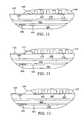
- FIG. 1is a cutaway cross-sectional view of a portion of an information storage system in accordance with a first embodiment of the present invention.
- FIG. 2is a cutaway cross-sectional view of a portion of an information storage system in accordance with a second embodiment of the present invention.
- FIG. 3is a cutaway cross-sectional view of a portion of an information storage system in accordance with a third embodiment of the present invention.
- FIG. 4is a cutaway cross-sectional view of portion of an information storage system in accordance with a fourth embodiment of the present invention.
- FIG. 5is a step in making an embodiment of the present invention having an inorganic nonferromagnetic apex region.
- FIG. 6is a step in making the embodiment of FIG. 5 subsequent to the step shown in FIG. 5 .
- FIG. 7is a step in making the embodiment of FIG. 5 and FIG. 6 subsequent to the step shown in FIG. 6 .
- FIG. 8is a step in making the embodiment of FIG. 5, FIG. 6 and FIG. 7 subsequent to the step shown in FIG. 7 .
- FIG. 9is a step in making another embodiment of the present invention having an inorganic nonferromagnetic apex region.
- FIG. 10is a step in making the embodiment of FIG. 9 subsequent to the step shown in FIG. 10 .
- FIG. 11is a step in making another embodiment of the present invention having an inorganic nonferromagnetic apex region.
- FIG. 12is a step in making another embodiment the present invention having an inorganic nonferromagnetic apex region.
- FIG. 13is a step in making another embodiment of the present invention having an inorganic nonferromagnetic apex region.
- FIG. 1depicts a cutaway cross-section of a portion of an information storage system 20 in accordance with an embodiment of the present invention.
- Portions of an electromagnetic head including a merged inductive and MR transducer 22are depicted in close proximity to a relatively moving media such as a spinning disk 25 .
- the transducer 22is formed in a plurality of adjoining solid layers on a wafer substrate 28 that may remain affixed to the transducer 22 . In this case, the substrate 28 is so much larger than the transducer 22 that a leading end 84 of the head is shown cut away from a trailing end 82 .
- a media-facing surface 33 of the solid body that includes the transducer 22may be formed with a desired relief for fluid and solid interaction with the disk 25 , and the body may be termed a head or slider.
- the disk 25may be conventional and includes a self-supporting substrate 35 , an underlayer 34 , a media layer 37 and a protective overcoat 39 .
- the disk 25is spinning in a direction indicated by arrow 31 and has a surface 32 adjacent the media-facing surface 33 of the head.
- the diskwhich is much larger than the head, is also shown in FIG. 1 cut into two portions.
- an undercoat layer 29 of SiO 2 or SiCis formed by sputtering or other low-pressure deposition processes, and then polished to a thickness of several (typically 2-6) microns (um). Formation of an undercoat layer 29 of silicon dioxide or silicon carbide rather than conventional alumina can result in a significant reduction in pole tip protrusion, even if no other changes to the head are made. This effect is also described in an article entitled “On the Thermal Behavior of Giant Magnetoresistive Heads,” by B. K. Gupta et al., Transactions of the ASME, Vol. 123, April 2001, pp. 380-387, which is incorporated herein by reference.
- an alumina undercoatcan be formed to have a reduced but nonzero thickness (in a range between three and four microns for current state of the art commercially available heads) to reduce pole tip protrusion.
- Various means for reducing pole tip protrusionare also described in the U.S. Patent Application filed by Express Mail Label No. EL928365990U.S. concurrently herewith, by inventors Arshad Alfoqaha et al., entitled “Inductive Transducer with Reduced Pole Tip Protrusion,” which is incorporated herein by reference.
- a low-coercivity, high-permeability or “soft magnetic” shield layer 30has been formed atop the undercoat 29 , the shield layer 30 made for example of permalloy.
- a first layer of nonferromagnetic, electrically insulating materialhas been formed on the shield layer 30 , followed by a magnetoresistive (MR) sensor 44 .
- MRmagnetoresistive
- the MR sensor 44can be any sensor that utilizes a change in resistance associated with a change in magnetic field to sense that field, which may be measured as a change in current or voltage across the sensor, including anisotropic magnetoresistive (AMR) sensors, spin-valve (SV) sensors, spin-tunneling (ST) sensors, giant magnetoresistive (GMR) sensors and colossal magnetoresistive (CMR) sensors.
- AMRanisotropic magnetoresistive
- SVspin-valve
- STspin-tunneling
- GMRgiant magnetoresistive
- CMRcolossal magnetoresistive
- a second layer of nonferromagnetic, electrically insulating materialhas been formed between the MR sensor and a second soft magnetic shield layer 46 , which also serves as a first pole layer 46 in this example of a merged head.
- the first and second layers of nonferromagnetic, electrically insulating materialare indicated together as region 40 and may be made, for example, of Al 2 O 3 , SiO 2 , AlN, or various forms of carbon-containing material, such as silicon carbide (SiC), diamond-like carbon (DLC) or tetrahedral amorphous carbon (ta-C).
- An electrically conductive coil layer 52has coil sections 55 that are separated from the shield/pole layer 46 by recording gap layer 57 , which may in this embodiment be formed of dielectric material such as Al 2 O 3 , SiO 2 , AlN, SiC, DLC or ta-C.
- Inorganic nonferromagnetic material 64having a coefficient of thermal expansion substantially less than that of hardbaked photoresist is formed in an apex region 66 .
- the term inorganic material in the present applicationrefers to a material that is lacking carbon polymer chains.
- Such inorganic material 64can be formed of dielectrics such as SiO 2 , SiC, Al 2 O 3 , Si 3 N 4 , TiC, AlN or metals such as Ta, W, Al, Ti, Au, Ni, Pd, Pt, Cr or NiCr.
- the apex region 66has a trailing surface 67 that is angled compared to the first pole layer 46 , such that along surface 67 an increase in distance from the leading end 84 corresponds to an increase in distance from the media-facing surface 33 .
- the angle of the trailing surface 67 compared to a normal to the media-facing surfacemay range between about 15° and about 75° in this embodiment.
- Silicon carbidehas a coefficient of thermal expansion at normal operating temperatures that is less than one-half that of alumina, and silicon dioxide has a coefficient of thermal expansion that is about one-seventh that of alumina.
- aluminahas a coefficient of thermal expansion that is about one-thirteenth that of hardbaked photoresist
- tantalumhas a coefficient of thermal expansion that is less than one-eighth that of hardbaked photoresist
- silicon carbidehas a coefficient of thermal expansion that is less than one-tenth that of hardbaked photoresist
- silicon dioxidehas a coefficient of thermal expansion that is about one-hundredth that of hardbaked photoresist.
- Hardbaked photoresist 68is disposed in a region between, around and atop coil sections 55 .
- a second soft magnetic pole layer 60is coupled to the first pole layer 46 by a soft magnetic stud 62 .
- a submicron, nonferromagnetic gap 70separates pole layers 46 and 60 adjacent to the media-facing surface 33 , the gap extending away from that surface 33 along a throat 72 , with the separation between pole layers 46 and 60 widening in the apex region 66 .
- a protective coating 80is formed on a trailing edge 82 of the body, while another protective coating 88 is formed on the media-facing surface 33 .
- Formation of the inorganic nonferromagnetic material 64 in apex region 66may be accomplished with various deposition and removal techniques. For example, a layer of the material 64 can be formed on a recording gap layer 57 of different material, after which a mask is formed over the apex region 66 . An isotropic etch can then be performed with a chemical that removes the material 64 but not the material of recording gap layer 57 , the etch terminated when all of the material 64 has been removed except for a mound or ridge 64 that is to remain in apex region 66 .
- a lift-off maskcan be formed on the recording gap layer 57 to have an opening over apex region 66 .
- Inorganic nonferromagnetic materialsuch as Al 2 O 3 , SiO 2 , AlN, SiC, DLC, Si 3 N 4 , Ta, Ti, TiC or Cr can then be sputtered onto the mask and through the opening in apex region 66 and onto the recording gap layer.
- the maskwhich may include plural layers for controlling the slope of the sides of the material formed in apex region 66 as well as for ease in mask removal, is then chemically removed and the sputtered material atop the mask lifted off, leaving a pyramid, ridge or wedge 64 .
- a layer of inorganic nonferromagnetic material 64can be formed on a recording gap layer 57 of different material, after which a photoresist mask is formed over the apex region 66 .
- the photoresist maskis then cured to create a hardbaked mask having sides with a slope similar to that desired for the apex region 66 .
- An anisotropic etchsuch as RIE or IBE is then directed substantially perpendicular to the wafer surface, forming material 64 into a replica of the baked mask in apex region 66 .
- recording gap layer 57is shown as extending between the material 64 in apex region 66 and shield/pole layer 46 , the material 64 may instead adjoin that layer 46 , with another nonferromagnetic layer forming a submicron recording gap separate from layer 57 .
- the coil layercan be formed by seeding, forming a coil mask and electroplating through the mask, after which the seed layer can be removed by IBE or RIE.
- a similar electroplating processcan be used to form soft magnetic stud 62 .
- Photoresist 68can then be deposited between the coil sections 55 and cured to form baked photoresist insulation 68 .
- the second pole layer 60can then be formed atop the gap 70 , apex region 66 , baked photoresist 68 and stud 62 by seeding and electroplating permalloy, for example.
- Further reduction in pole tip protrusionmay be accomplished, for example, by filling at least portions of the regions between the coil sections 55 with photoresist, and then depositing inorganic dielectric such as silicon dioxide onto the coil sections 55 and into any spaces between the coil sections 55 .
- the photoresistcan be spun and cured to fill the regions between the coil sections 55 without remaining atop the coil sections 55 . Encircling the baked photoresist between the coil sections 55 with relatively hard inorganic material having a lower coefficient of thermal expansion than the photoresist may further constrain expansion of the photoresist. Additional reduction in pole tip protrusion is achieved in this case due to the substitution of the photoresist with the less thermally expansive material.
- FIG. 2shows an information storage system 100 with a transducer 102 in which the apex region 66 and insulation surrounding coil sections 55 are formed of inorganic dielectric material 105 having a lower coefficient of thermal expansion than baked photoresist, such as alumina or silicon dioxide.
- a tapered apex region 66can be formed of inorganic material 105 shaped by a lift-off process or chemical etching, as described above. In either case, additional insulation material can be formed of baked photoresist or additional inorganic insulation.
- the transducer 102may partially completed by conventional means (aside from forming the novel undercoat layer 29 of SiO 2 ), including forming the shield/pole layer 46 of permalloy having a thickness of a few microns or less.
- a submicron nonferromagnetic gap layer 103may then be formed on the shield/pole layer 46 to a thickness that may be in a range between 50 nanometers (nm) and 500 rm.
- the coil layer 52may then be formed by sputtering a conductive seed layer, forming a photoresist with a spiral void through which the coil is electroplated, chemically removing the resist and removing the seed by ion beam etching (IBE, reactive ion etching or the like.
- IBEion beam etching
- a lift-off mask(preferably bi-layer) may then be formed over the throat area 72 and inorganic dielectric such as silicon dioxide is sputtered over and between the coil sections 55 .
- inorganic dielectricsuch as silicon dioxide
- a surface 90may result that in some places does not extend above the coil sections 55 in areas between the coil sections 55 . It is also possible to remove some of first pole layer 46 by IBE prior to sputtering inorganic dielectric over and between the coil sections 55 .
- a photoresist maskcan be formed over the coil sections, the photoresist mask then spun to fill in the depressions and cured to form baked photoresist filler 107 .
- layer of inorganic dielectricsuch as silicon dioxide can be sputtered over and between the coil sections 55 , and then polished to form a flat surface above the coil sections 55 .
- a maskcan then be formed over coil sections 55 , the mask terminating above throat 72 .
- an isotropic etchcan be performed with a chemical that removes the inorganic dielectric but not recording gap layer 103 , the etch terminated when all of the inorganic dielectric has been removed above throat 72 , creating a sloping apex region 66 that leads to the thicker inorganic dielectric layer remaining between and above coil sections 55 .
- the apex region 66provides for smoothly increasing the separation of the first and second pole layers from less than a micron to greater than a micron as said pole layers extend from the media-facing surface 33 .
- FIG. 3shows an information storage system 200 with a transducer 202 having a second coil layer 207 and a stitched second pole layer 210 .
- Shield layer 29is formed of silicon dioxide and has a thickness of between two and four microns.
- transducer 200has a first shield layer 212 that is much thinner than merged shield/pole layer 46 .
- silicon dioxide or other dielectrichaving a lower thermal expansion coefficient than permalloy may be formed.
- a layer 214 of silicon carbidemay be formed between shield layer 212 , silicon carbide affording greater thermal conductivity and lower thermal expansion than alumina.
- a nonferromagnetic insulating gap layer 208has been formed, on which the apex region 66 is formed of inorganic material 205 that has a lower coefficient of thermal expansion than that of baked photoresist, such as alumina or silicon dioxide.
- the tapered apex region 66can be formed of inorganic nonferromagnetic material 205 shaped by a lift-off process, chemical etching or replication etching, as described above.
- the transducercan be formed as described in U.S. patent application Ser. No. 09/999,694, filed Oct. 24, 2001, inventors Yingjian Chen et al., entitled “Inductive Transducer with Stitched Pole Tip and Pedestal Defining Zero Throat Height,” which is incorporated herein by reference.
- inorganic nonferromagnetic material 205is formed separately from insulation between and around coil sections 55 , that insulation can be formed on and around coil sections 55 of baked photoresist and/or inorganic material.
- a magnetic layer cbe seeded and plated, the magnetic layer and additional insulation material then polished to form surface 219 and a second pole layer 222 including a trailing pole tip.
- Second coil layer 207can then be formed including coil sections 221 , and additional insulation 215 can be formed partly or wholly of organic or inorganic material, as described above. Atop insulation 215 , second pole layer 222 and magnetic stud 62 , a third pole layer 210 can then be formed. In this embodiment as well as others, providing a relatively thick (e.g., 20-40 micron) coating 80 on the trailing end 82 can be advantageous in constraining pole tip protrusion.
- a relatively thick (e.g., 20-40 micron) coating 80 on the trailing end 82can be advantageous in constraining pole tip protrusion.
- first shield layer 30becomes more constrained by the substrate 28 , which has a lower coefficient of thermal expansion, lowering the pole tip protrusion.
- first shield layer 30becomes more constrained by the substrate 28 , which has a lower coefficient of thermal expansion, lowering the pole tip protrusion.
- the layers above first shield layer 30are constrained similar to but proportionally less than first shield layer 30 . This tends to decrease the contribution of second shield and first pole layer 46 to the pole tip protrusion.
- a second countervailing conditionbecomes apparent at small undercoat 29 thicknesses.
- the relatively rigid second pole layer 60 and overcoat layer 80 region near the media-facing surface 33pivots about the write gap 70 due to expansion of hardbaked photoresist about the coil sections 55 , so that the trailing end 32 of the head protrudes toward the disk surface 32 .
- the first conditiontends to dominate for undercoat 29 thicknesses greater than a few microns.
- the second conditiontends to dominate for undercoat 29 thicknesses less than a few microns.
- FIG. 4shows an information storage system 300 having a piggyback head 303 in accordance with the present invention.
- This embodimentincludes several novel features that may be used individually, or in the combination shown, or combined with other features described and depicted in other embodiments.
- an undercoat layer 29 of silicon dioxidehas been formed to a thickness of about three microns.
- the embodiment shown in FIG. 4also includes a spin-dependent tunneling sensor 304 that may alternatively be used in other embodiments.
- a second shield layer 306has been formed adjacent the sensor 304 , the second shield layer 306 extending from the media-facing surface 33 much less than the first shield 30 or a first pole layer 313 .
- a back shield layer 308is formed of a material having a lower coefficient of thermal expansion than permalloy, such as silicon dioxide or other insulator, conductor or semiconductor materials, which may include Ta, Pd, Pt, or Al 2 O 3 , for example.
- a read gap insulator layer 310such as silicon dioxide separates the first shield 30 from the second shield layer 306 and the back shield layer 308 .
- the first pole layer 313is separated from the second shield layer 306 and the back shield layer 308 in this embodiment by a piggyback gap layer 315 .
- the piggyback gap layer 315is formed of silicon dioxide rather than conventional alumina, this substitution by itself providing a measurable decrease in pole tip protrusion of a few nanometers.
- a submicron, nonferromagnetic write gap layer 318is formed on the first pole layer 315 , the write gap layer 318 formed of dielectric material such as alumina or silicon carbide, or conductive material such as Ta, Pd, Pt, NiCr or NiFeCr.
- An inorganic apex region 320has been formed by etching, lift-off deposition or replication etching as described above, after which a first coil layer 322 , including coil sections 325 , has been formed.
- a layer of baked photoresist 330fills the area between coil sections 325 , and an inorganic dielectric material layer 333 is disposed atop the photoresist 330 .
- a second pole layer 335 including a trailing pole tip as well as a back gap stud 337have been formed of soft magnetic material and polished along with the inorganic dielectric material layer 333 to form a flat surface 338 .
- the photoresist 330provides thorough coverage in the corners between the coil sections 325 , whereas the inorganic dielectric material 333 constrains the thermal expansion of the photoresist 330 .
- Atop surface 338 another inorganic region 340has been formed by etching or lift-off deposition as described above, after which a second coil layer 342 , including coil sections 344 , has been formed.
- a layer of baked photoresist 350fills the area between coil sections 344 , and an inorganic dielectric material layer 353 is disposed atop the photoresist 330 .
- a stitch pole layer 355 as well as another back gap stud 357have been formed of soft magnetic material and polished along with the inorganic dielectric material layer 333 to form another flat surface.
- a trailing pole layer 360 of soft magnetic materialis then formed, followed by a thick (e.g., 20 um-40 um) coating layer 366 on a trailing end 362 .
- FIG. 5shows a step in making an embodiment of the present invention having an inorganic nonferromagnetic apex region.
- a first shield layer 400is insulated from a second shield layer 402 by inorganic dielectric layer 404 , with an MR sensor 406 also disposed between the first and second shield layers.
- a first pole layer 410is spaced apart from second shield layer 402 by a silicon dioxide piggyback layer 408 .
- Atop the fist pole layeran inorganic dielectric layer 412 has been formed, for example by sputtering alumina to a thickness of one-quarter micron though a mask that has been lifted off to leave the layer 412 shown.
- a layer 414 of inorganic nonferromagnetic material such as silicon dioxide or tantalumhas been formed on the first pole layer 410 and dielectric layer 412 .
- Layer 414may be formed by physical vapor deposition (PVD) such as sputtering, plasma enhanced chemical vapor deposition (PECVD) or other known techniques.
- PVDphysical vapor deposition
- PECVDplasma enhanced chemical vapor deposition
- a replication mask 416 of baked photoresisthas been formed into a desired shape for creating an apex region from layer 414 . Since mask 416 is made of baked photoresist it can be easily formed by photolithography and curing into the desired shape. An ion-assisted etch is then performed in the direction of arrows 418 , for example by RIE with at least partially ionized gases of O 2 and CHF 3 , O 2 and CF 4 or O 2 and CF 4 .
- the bake photoresisthas a similar rate of removal during ion-assisted etching as the inorganic nonferromagnetic material of layer 414 , so that the shape of replication mask 416 is transferred to layer 414 to create apex region 420 shown in FIG. 6 .
- the RIEis designed to be highly selective between silicon dioxide and alumina or tantalum, with an etch rate selectivity of about ten or twenty for silicon dioxide to alumina, for example.
- the silicon dioxideis removed by the RIE at a rate about ten to twenty times as fast as the rate of removal of alumina.
- Nickel ironis etched even slower by the RIE, because nickel iron does not react with the etch chemicals, but may experience slight removal due to ion impingement.
- both layer 410 and layer 412can serve as etch stops for the RIE.
- Optical measurement and monitoringcan be used to indicate completion of the RIE.
- FIG. 6shows just one example of an inorganic nonferromagnetic apex shape 420 that can be formed with this mask transfer process. Note that the inorganic nonferromagnetic apex region 420 has a sloping side 421 that is neither parallel nor perpendicular to a surface 427 of first pole layer 410 .
- FIG. 7shows a set of coil sections 422 formed on inorganic dielectric layer 412 as part of a coil layer, for example by electroplating through a photoresist mask that is removed to allow IBE of the seed layer for the coil layer.
- a recording gap layer 424 of inorganic nonferromagnetic materialhas been formed on first pole layer 410 and apex bump 420 .
- a layer of photoresist 426has been deposited and cured between and atop coil sections 422 .
- a second pole layercan then be formed, as described above.
- FIG. 8shows baked photoresist 426 between the coil sections 422 , this insulation can instead or in addition be made with inorganic materials, as described above.
- FIG. 9shows a step in forming an inorganic nonferromagnetic apex region with IBE.
- layers 412 and 414can be composed of a wider variety of materials than those for RIE processes.
- Inorganic dielectric layer 412can be made of AlN, Si 3 N 4 , SiC or SiO 2 , for example.
- Inorganic nonferromagnetic layer 414can be made of those dielectric materials or metals such as Cr, Au, Cu, Ta, Pt, Pd and their alloys, e.g., NiCr.
- the IBEwhich may be called ion milling, may be performed with Ar ions at a fixed, sweeping or rotating angle to the wafer surface.
- the ionsare directed at an angle that is approximately 45° to the wafer surface, the angle rotating at approximately 45° about a normal to that surface. That is at one time the ions are directed at an angle shown by arrows 450 , and at a later time the ions are directed at an angle shown by arrows 452 .
- Such an angled IBEhomogenizes the etch rate of various materials.
- an IBE etch rate of silicon dioxideis similar to that or baked photoresist for an IBE directed perpendicular to the wafer surface, and about equal to that of baked photoresist for an etch directed at 45° to perpendicular.
- an IBE etch rate of aluminais close to that of baked photoresist for an IBE directed perpendicular to the wafer surface, and essentially identical to that of baked photoresist for an etch directed at 45° to perpendicular. Although an angle of about 45° is listed in the above example, etch angles in a range between about 12° and about 70° have been found favorable. Termination of etching may be assisted by monitoring gases discharged from the etching chamber for the presence of chemicals from layers 412 or 414 to indicate completion of the IBE.
- the replication maskneed not have an identical shape to that desired for the apex bump, but instead the mask shape and etching process can compensate for each other to yield a desired apex bump. Note also that various other shapes can be made with such a mask transfer processes.
- a dielectric submicron gap layer 460has been formed prior to an inorganic nonferromagnetic layer that has been etched after being covered with a transfer mask to form an inorganic nonferromagnetic apex region 464 .
- Hardbaked photoresist 466has been formed between and atop coil sections 462 in this example.
- FIG. 12shows an alternative embodiment in which an inorganic nonferromagnetic layer has been formed on a first pole layer 470 , covered with a transfer mask, and etched to form an inorganic nonferromagnetic apex region 474 .
- An inorganic dielectric layer 476has been formed atop apex region 474 and first pole 470 , after which coil sections 472 were formed.
- Hardbaked photoresist 478has also been formed between and atop coil sections 472 in this example.
- FIG. 13shows an embodiment in which an inorganic nonferromagnetic dielectric layer has been formed on a first pole layer 480 , covered with a transfer mask, and etched to form an inorganic nonferromagnetic apex region 484 as well as a submicron gap layer 486 .
- a portion of the submicron gap layerextends to separate first pole layer 480 from coil sections 482 .
- Hardbaked photoresist 488has also been formed between and atop coil sections 482 in this example.
Landscapes
- Engineering & Computer Science (AREA)
- Manufacturing & Machinery (AREA)
- Magnetic Heads (AREA)
Abstract
Description
Claims (20)
Priority Applications (1)
| Application Number | Priority Date | Filing Date | Title |
|---|---|---|---|
| US10/042,673US6737281B1 (en) | 2002-01-08 | 2002-01-08 | Method of making transducer with inorganic nonferromagnetic apex region |
Applications Claiming Priority (1)
| Application Number | Priority Date | Filing Date | Title |
|---|---|---|---|
| US10/042,673US6737281B1 (en) | 2002-01-08 | 2002-01-08 | Method of making transducer with inorganic nonferromagnetic apex region |
Publications (1)
| Publication Number | Publication Date |
|---|---|
| US6737281B1true US6737281B1 (en) | 2004-05-18 |
Family
ID=32296375
Family Applications (1)
| Application Number | Title | Priority Date | Filing Date |
|---|---|---|---|
| US10/042,673Expired - LifetimeUS6737281B1 (en) | 2002-01-08 | 2002-01-08 | Method of making transducer with inorganic nonferromagnetic apex region |
Country Status (1)
| Country | Link |
|---|---|
| US (1) | US6737281B1 (en) |
Cited By (148)
| Publication number | Priority date | Publication date | Assignee | Title |
|---|---|---|---|---|
| US20040070870A1 (en)* | 2002-10-15 | 2004-04-15 | International Business Machines | Magnetic recording heads having thin thermally conductive undercoating |
| US20040085674A1 (en)* | 2002-10-31 | 2004-05-06 | Headway Technologies, Inc. | Self-aligned pole trim process |
| US20040179286A1 (en)* | 2001-09-07 | 2004-09-16 | Samsung Electronics Co., Ltd. | Dummy write method for improving performance of data storage system and apparatus therefor |
| US20040252412A1 (en)* | 2003-06-16 | 2004-12-16 | Seagate Technology Llc | Patterned multi-material basecoat to reduce thermal protrusion |
| US6900963B1 (en)* | 1999-07-06 | 2005-05-31 | Alps Electric Co., Ltd. | Thin film magnetic head with track width restricting groove formed to fully reach lower core layer, and manufacturing method for the same |
| US20050219765A1 (en)* | 2004-04-02 | 2005-10-06 | Tdk Corporation | Composite type thin-film magnetic head |
| US20050238929A1 (en)* | 2004-04-16 | 2005-10-27 | Fuji Electric Device | Disk substrate for a perpendicular magnetic recording medium and a perpendicular magnetic recording medium using the substrate |
| US6960480B1 (en)* | 2004-05-19 | 2005-11-01 | Headway Technologies, Inc. | Method of forming a magnetic tunneling junction (MTJ) MRAM device and a tunneling magnetoresistive (TMR) read head |
| US20050287304A1 (en)* | 2004-06-11 | 2005-12-29 | Fuji Electric Device Technology Co., | Method of treating a substrate for electroless plating and method of increasing adhesion therebetween, and magnetic recording medium and magnetic recording device thereof |
| US20060024431A1 (en)* | 2004-07-27 | 2006-02-02 | Fuji Electric Device | Method of manufacturing a disk substrate for a magnetic recording medium |
| US20060210837A1 (en)* | 2004-04-16 | 2006-09-21 | Fuji Electric Device | Method of plating on a glass base plate, a method of manufacturing a disk substrate for a perpendicular magnetic recording medium, a disk substrate for a perpendicular magnetic recording medium, and a perpendicular magnetic recording medium |
| US20060228493A1 (en)* | 2005-04-08 | 2006-10-12 | Fuji Electric Device Technology Co., Ltd. | Method of plating on a glass base plate and a method of manufacturing a perpendicular magnetic recording medium |
| US7248433B1 (en)* | 2004-02-02 | 2007-07-24 | Western Digital (Fremont), Inc. | Magnetic head with stitched top pole layer and single layer coil or solenoidal coil |
| US20070247749A1 (en)* | 2006-04-25 | 2007-10-25 | Bonhote Christian R | Structure and method for reduced corrosion of auxiliary poles during the fabrication of perpendicular write heads |
| US20080068762A1 (en)* | 2006-09-20 | 2008-03-20 | Kiyoshi Kobayashi | Thin film magnetic head including thermal deformation-preventing layer |
| US20100002339A1 (en)* | 2008-07-04 | 2010-01-07 | Fujitsu Limited | Head slider, magnetic storage apparatus and method of fabricating head slider |
| US8607438B1 (en) | 2011-12-01 | 2013-12-17 | Western Digital (Fremont), Llc | Method for fabricating a read sensor for a read transducer |
| US8790524B1 (en) | 2010-09-13 | 2014-07-29 | Western Digital (Fremont), Llc | Method and system for providing a magnetic recording transducer using a line hard mask and a wet-etchable mask |
| US8830628B1 (en) | 2009-02-23 | 2014-09-09 | Western Digital (Fremont), Llc | Method and system for providing a perpendicular magnetic recording head |
| US8879207B1 (en) | 2011-12-20 | 2014-11-04 | Western Digital (Fremont), Llc | Method for providing a side shield for a magnetic recording transducer using an air bridge |
| US8883017B1 (en) | 2013-03-12 | 2014-11-11 | Western Digital (Fremont), Llc | Method and system for providing a read transducer having seamless interfaces |
| US8917581B1 (en) | 2013-12-18 | 2014-12-23 | Western Digital Technologies, Inc. | Self-anneal process for a near field transducer and chimney in a hard disk drive assembly |
| US8923102B1 (en) | 2013-07-16 | 2014-12-30 | Western Digital (Fremont), Llc | Optical grating coupling for interferometric waveguides in heat assisted magnetic recording heads |
| US8947985B1 (en) | 2013-07-16 | 2015-02-03 | Western Digital (Fremont), Llc | Heat assisted magnetic recording transducers having a recessed pole |
| US8953422B1 (en) | 2014-06-10 | 2015-02-10 | Western Digital (Fremont), Llc | Near field transducer using dielectric waveguide core with fine ridge feature |
| US8958272B1 (en) | 2014-06-10 | 2015-02-17 | Western Digital (Fremont), Llc | Interfering near field transducer for energy assisted magnetic recording |
| US8971160B1 (en) | 2013-12-19 | 2015-03-03 | Western Digital (Fremont), Llc | Near field transducer with high refractive index pin for heat assisted magnetic recording |
| US8970988B1 (en) | 2013-12-31 | 2015-03-03 | Western Digital (Fremont), Llc | Electric gaps and method for making electric gaps for multiple sensor arrays |
| US8976635B1 (en) | 2014-06-10 | 2015-03-10 | Western Digital (Fremont), Llc | Near field transducer driven by a transverse electric waveguide for energy assisted magnetic recording |
| US8980109B1 (en) | 2012-12-11 | 2015-03-17 | Western Digital (Fremont), Llc | Method for providing a magnetic recording transducer using a combined main pole and side shield CMP for a wraparound shield scheme |
| US8982508B1 (en) | 2011-10-31 | 2015-03-17 | Western Digital (Fremont), Llc | Method for providing a side shield for a magnetic recording transducer |
| US8988825B1 (en) | 2014-02-28 | 2015-03-24 | Western Digital (Fremont, LLC | Method for fabricating a magnetic writer having half-side shields |
| US8988812B1 (en) | 2013-11-27 | 2015-03-24 | Western Digital (Fremont), Llc | Multi-sensor array configuration for a two-dimensional magnetic recording (TDMR) operation |
| US8984740B1 (en) | 2012-11-30 | 2015-03-24 | Western Digital (Fremont), Llc | Process for providing a magnetic recording transducer having a smooth magnetic seed layer |
| US8995087B1 (en) | 2006-11-29 | 2015-03-31 | Western Digital (Fremont), Llc | Perpendicular magnetic recording write head having a wrap around shield |
| US8993217B1 (en) | 2013-04-04 | 2015-03-31 | Western Digital (Fremont), Llc | Double exposure technique for high resolution disk imaging |
| US8997832B1 (en) | 2010-11-23 | 2015-04-07 | Western Digital (Fremont), Llc | Method of fabricating micrometer scale components |
| US9001467B1 (en) | 2014-03-05 | 2015-04-07 | Western Digital (Fremont), Llc | Method for fabricating side shields in a magnetic writer |
| US9001628B1 (en) | 2013-12-16 | 2015-04-07 | Western Digital (Fremont), Llc | Assistant waveguides for evaluating main waveguide coupling efficiency and diode laser alignment tolerances for hard disk |
| US9007719B1 (en) | 2013-10-23 | 2015-04-14 | Western Digital (Fremont), Llc | Systems and methods for using double mask techniques to achieve very small features |
| US9007879B1 (en) | 2014-06-10 | 2015-04-14 | Western Digital (Fremont), Llc | Interfering near field transducer having a wide metal bar feature for energy assisted magnetic recording |
| US9007725B1 (en) | 2014-10-07 | 2015-04-14 | Western Digital (Fremont), Llc | Sensor with positive coupling between dual ferromagnetic free layer laminates |
| US9013836B1 (en) | 2013-04-02 | 2015-04-21 | Western Digital (Fremont), Llc | Method and system for providing an antiferromagnetically coupled return pole |
| US9042052B1 (en) | 2014-06-23 | 2015-05-26 | Western Digital (Fremont), Llc | Magnetic writer having a partially shunted coil |
| US9042058B1 (en) | 2013-10-17 | 2015-05-26 | Western Digital Technologies, Inc. | Shield designed for middle shields in a multiple sensor array |
| US9042208B1 (en) | 2013-03-11 | 2015-05-26 | Western Digital Technologies, Inc. | Disk drive measuring fly height by applying a bias voltage to an electrically insulated write component of a head |
| US9042057B1 (en) | 2013-01-09 | 2015-05-26 | Western Digital (Fremont), Llc | Methods for providing magnetic storage elements with high magneto-resistance using Heusler alloys |
| US9042051B2 (en) | 2013-08-15 | 2015-05-26 | Western Digital (Fremont), Llc | Gradient write gap for perpendicular magnetic recording writer |
| US9053735B1 (en) | 2014-06-20 | 2015-06-09 | Western Digital (Fremont), Llc | Method for fabricating a magnetic writer using a full-film metal planarization |
| US9064528B1 (en) | 2013-05-17 | 2015-06-23 | Western Digital Technologies, Inc. | Interferometric waveguide usable in shingled heat assisted magnetic recording in the absence of a near-field transducer |
| US9065043B1 (en) | 2012-06-29 | 2015-06-23 | Western Digital (Fremont), Llc | Tunnel magnetoresistance read head with narrow shield-to-shield spacing |
| US9064527B1 (en) | 2013-04-12 | 2015-06-23 | Western Digital (Fremont), Llc | High order tapered waveguide for use in a heat assisted magnetic recording head |
| US9064507B1 (en) | 2009-07-31 | 2015-06-23 | Western Digital (Fremont), Llc | Magnetic etch-stop layer for magnetoresistive read heads |
| US9070381B1 (en) | 2013-04-12 | 2015-06-30 | Western Digital (Fremont), Llc | Magnetic recording read transducer having a laminated free layer |
| US9082423B1 (en) | 2013-12-18 | 2015-07-14 | Western Digital (Fremont), Llc | Magnetic recording write transducer having an improved trailing surface profile |
| US9087527B1 (en) | 2014-10-28 | 2015-07-21 | Western Digital (Fremont), Llc | Apparatus and method for middle shield connection in magnetic recording transducers |
| US9087534B1 (en) | 2011-12-20 | 2015-07-21 | Western Digital (Fremont), Llc | Method and system for providing a read transducer having soft and hard magnetic bias structures |
| US9093639B2 (en) | 2012-02-21 | 2015-07-28 | Western Digital (Fremont), Llc | Methods for manufacturing a magnetoresistive structure utilizing heating and cooling |
| US9104107B1 (en) | 2013-04-03 | 2015-08-11 | Western Digital (Fremont), Llc | DUV photoresist process |
| US9111550B1 (en) | 2014-12-04 | 2015-08-18 | Western Digital (Fremont), Llc | Write transducer having a magnetic buffer layer spaced between a side shield and a write pole by non-magnetic layers |
| US9111558B1 (en) | 2014-03-14 | 2015-08-18 | Western Digital (Fremont), Llc | System and method of diffractive focusing of light in a waveguide |
| US9111564B1 (en) | 2013-04-02 | 2015-08-18 | Western Digital (Fremont), Llc | Magnetic recording writer having a main pole with multiple flare angles |
| US9123358B1 (en) | 2012-06-11 | 2015-09-01 | Western Digital (Fremont), Llc | Conformal high moment side shield seed layer for perpendicular magnetic recording writer |
| US9123359B1 (en) | 2010-12-22 | 2015-09-01 | Western Digital (Fremont), Llc | Magnetic recording transducer with sputtered antiferromagnetic coupling trilayer between plated ferromagnetic shields and method of fabrication |
| US9123362B1 (en) | 2011-03-22 | 2015-09-01 | Western Digital (Fremont), Llc | Methods for assembling an electrically assisted magnetic recording (EAMR) head |
| US9123374B1 (en) | 2015-02-12 | 2015-09-01 | Western Digital (Fremont), Llc | Heat assisted magnetic recording writer having an integrated polarization rotation plate |
| US9135930B1 (en) | 2014-03-06 | 2015-09-15 | Western Digital (Fremont), Llc | Method for fabricating a magnetic write pole using vacuum deposition |
| US9135937B1 (en) | 2014-05-09 | 2015-09-15 | Western Digital (Fremont), Llc | Current modulation on laser diode for energy assisted magnetic recording transducer |
| US9142233B1 (en) | 2014-02-28 | 2015-09-22 | Western Digital (Fremont), Llc | Heat assisted magnetic recording writer having a recessed pole |
| US9147408B1 (en) | 2013-12-19 | 2015-09-29 | Western Digital (Fremont), Llc | Heated AFM layer deposition and cooling process for TMR magnetic recording sensor with high pinning field |
| US9147404B1 (en) | 2015-03-31 | 2015-09-29 | Western Digital (Fremont), Llc | Method and system for providing a read transducer having a dual free layer |
| US9153255B1 (en) | 2014-03-05 | 2015-10-06 | Western Digital (Fremont), Llc | Method for fabricating a magnetic writer having an asymmetric gap and shields |
| US9183854B2 (en) | 2014-02-24 | 2015-11-10 | Western Digital (Fremont), Llc | Method to make interferometric taper waveguide for HAMR light delivery |
| US9190079B1 (en) | 2014-09-22 | 2015-11-17 | Western Digital (Fremont), Llc | Magnetic write pole having engineered radius of curvature and chisel angle profiles |
| US9190085B1 (en) | 2014-03-12 | 2015-11-17 | Western Digital (Fremont), Llc | Waveguide with reflective grating for localized energy intensity |
| US9194692B1 (en) | 2013-12-06 | 2015-11-24 | Western Digital (Fremont), Llc | Systems and methods for using white light interferometry to measure undercut of a bi-layer structure |
| US9202493B1 (en) | 2014-02-28 | 2015-12-01 | Western Digital (Fremont), Llc | Method of making an ultra-sharp tip mode converter for a HAMR head |
| US9202480B2 (en) | 2009-10-14 | 2015-12-01 | Western Digital (Fremont), LLC. | Double patterning hard mask for damascene perpendicular magnetic recording (PMR) writer |
| US9214169B1 (en) | 2014-06-20 | 2015-12-15 | Western Digital (Fremont), Llc | Magnetic recording read transducer having a laminated free layer |
| US9214172B2 (en) | 2013-10-23 | 2015-12-15 | Western Digital (Fremont), Llc | Method of manufacturing a magnetic read head |
| US9213322B1 (en) | 2012-08-16 | 2015-12-15 | Western Digital (Fremont), Llc | Methods for providing run to run process control using a dynamic tuner |
| US9214165B1 (en) | 2014-12-18 | 2015-12-15 | Western Digital (Fremont), Llc | Magnetic writer having a gradient in saturation magnetization of the shields |
| US9230565B1 (en) | 2014-06-24 | 2016-01-05 | Western Digital (Fremont), Llc | Magnetic shield for magnetic recording head |
| US9236560B1 (en) | 2014-12-08 | 2016-01-12 | Western Digital (Fremont), Llc | Spin transfer torque tunneling magnetoresistive device having a laminated free layer with perpendicular magnetic anisotropy |
| US9245543B1 (en) | 2010-06-25 | 2016-01-26 | Western Digital (Fremont), Llc | Method for providing an energy assisted magnetic recording head having a laser integrally mounted to the slider |
| US9245545B1 (en) | 2013-04-12 | 2016-01-26 | Wester Digital (Fremont), Llc | Short yoke length coils for magnetic heads in disk drives |
| US9245562B1 (en) | 2015-03-30 | 2016-01-26 | Western Digital (Fremont), Llc | Magnetic recording writer with a composite main pole |
| US9251813B1 (en) | 2009-04-19 | 2016-02-02 | Western Digital (Fremont), Llc | Method of making a magnetic recording head |
| US9263071B1 (en) | 2015-03-31 | 2016-02-16 | Western Digital (Fremont), Llc | Flat NFT for heat assisted magnetic recording |
| US9263067B1 (en) | 2013-05-29 | 2016-02-16 | Western Digital (Fremont), Llc | Process for making PMR writer with constant side wall angle |
| US9269382B1 (en) | 2012-06-29 | 2016-02-23 | Western Digital (Fremont), Llc | Method and system for providing a read transducer having improved pinning of the pinned layer at higher recording densities |
| US9275657B1 (en) | 2013-08-14 | 2016-03-01 | Western Digital (Fremont), Llc | Process for making PMR writer with non-conformal side gaps |
| US9280990B1 (en) | 2013-12-11 | 2016-03-08 | Western Digital (Fremont), Llc | Method for fabricating a magnetic writer using multiple etches |
| US9286919B1 (en) | 2014-12-17 | 2016-03-15 | Western Digital (Fremont), Llc | Magnetic writer having a dual side gap |
| US9287494B1 (en) | 2013-06-28 | 2016-03-15 | Western Digital (Fremont), Llc | Magnetic tunnel junction (MTJ) with a magnesium oxide tunnel barrier |
| US9305583B1 (en) | 2014-02-18 | 2016-04-05 | Western Digital (Fremont), Llc | Method for fabricating a magnetic writer using multiple etches of damascene materials |
| US9312064B1 (en) | 2015-03-02 | 2016-04-12 | Western Digital (Fremont), Llc | Method to fabricate a magnetic head including ion milling of read gap using dual layer hard mask |
| US9318130B1 (en) | 2013-07-02 | 2016-04-19 | Western Digital (Fremont), Llc | Method to fabricate tunneling magnetic recording heads with extended pinned layer |
| US9336814B1 (en) | 2013-03-12 | 2016-05-10 | Western Digital (Fremont), Llc | Inverse tapered waveguide for use in a heat assisted magnetic recording head |
| US9343086B1 (en) | 2013-09-11 | 2016-05-17 | Western Digital (Fremont), Llc | Magnetic recording write transducer having an improved sidewall angle profile |
| US9343087B1 (en) | 2014-12-21 | 2016-05-17 | Western Digital (Fremont), Llc | Method for fabricating a magnetic writer having half shields |
| US9343098B1 (en) | 2013-08-23 | 2016-05-17 | Western Digital (Fremont), Llc | Method for providing a heat assisted magnetic recording transducer having protective pads |
| US9349394B1 (en) | 2013-10-18 | 2016-05-24 | Western Digital (Fremont), Llc | Method for fabricating a magnetic writer having a gradient side gap |
| US9349392B1 (en) | 2012-05-24 | 2016-05-24 | Western Digital (Fremont), Llc | Methods for improving adhesion on dielectric substrates |
| US9361914B1 (en) | 2014-06-18 | 2016-06-07 | Western Digital (Fremont), Llc | Magnetic sensor with thin capping layer |
| US9361913B1 (en) | 2013-06-03 | 2016-06-07 | Western Digital (Fremont), Llc | Recording read heads with a multi-layer AFM layer methods and apparatuses |
| US9368134B1 (en) | 2010-12-16 | 2016-06-14 | Western Digital (Fremont), Llc | Method and system for providing an antiferromagnetically coupled writer |
| US9384765B1 (en) | 2015-09-24 | 2016-07-05 | Western Digital (Fremont), Llc | Method and system for providing a HAMR writer having improved optical efficiency |
| US9384763B1 (en) | 2015-03-26 | 2016-07-05 | Western Digital (Fremont), Llc | Dual free layer magnetic reader having a rear bias structure including a soft bias layer |
| US9396743B1 (en) | 2014-02-28 | 2016-07-19 | Western Digital (Fremont), Llc | Systems and methods for controlling soft bias thickness for tunnel magnetoresistance readers |
| US9396742B1 (en) | 2012-11-30 | 2016-07-19 | Western Digital (Fremont), Llc | Magnetoresistive sensor for a magnetic storage system read head, and fabrication method thereof |
| US9406331B1 (en) | 2013-06-17 | 2016-08-02 | Western Digital (Fremont), Llc | Method for making ultra-narrow read sensor and read transducer device resulting therefrom |
| US9424866B1 (en) | 2015-09-24 | 2016-08-23 | Western Digital (Fremont), Llc | Heat assisted magnetic recording write apparatus having a dielectric gap |
| US9431038B1 (en) | 2015-06-29 | 2016-08-30 | Western Digital (Fremont), Llc | Method for fabricating a magnetic write pole having an improved sidewall angle profile |
| US9431032B1 (en) | 2013-08-14 | 2016-08-30 | Western Digital (Fremont), Llc | Electrical connection arrangement for a multiple sensor array usable in two-dimensional magnetic recording |
| US9431047B1 (en) | 2013-05-01 | 2016-08-30 | Western Digital (Fremont), Llc | Method for providing an improved AFM reader shield |
| US9431031B1 (en) | 2015-03-24 | 2016-08-30 | Western Digital (Fremont), Llc | System and method for magnetic transducers having multiple sensors and AFC shields |
| US9431039B1 (en) | 2013-05-21 | 2016-08-30 | Western Digital (Fremont), Llc | Multiple sensor array usable in two-dimensional magnetic recording |
| US9437251B1 (en) | 2014-12-22 | 2016-09-06 | Western Digital (Fremont), Llc | Apparatus and method having TDMR reader to reader shunts |
| US9441938B1 (en) | 2013-10-08 | 2016-09-13 | Western Digital (Fremont), Llc | Test structures for measuring near field transducer disc length |
| US9443541B1 (en) | 2015-03-24 | 2016-09-13 | Western Digital (Fremont), Llc | Magnetic writer having a gradient in saturation magnetization of the shields and return pole |
| US9449625B1 (en) | 2014-12-24 | 2016-09-20 | Western Digital (Fremont), Llc | Heat assisted magnetic recording head having a plurality of diffusion barrier layers |
| US9449621B1 (en) | 2015-03-26 | 2016-09-20 | Western Digital (Fremont), Llc | Dual free layer magnetic reader having a rear bias structure having a high aspect ratio |
| US9472216B1 (en) | 2015-09-23 | 2016-10-18 | Western Digital (Fremont), Llc | Differential dual free layer magnetic reader |
| US9484051B1 (en) | 2015-11-09 | 2016-11-01 | The Provost, Fellows, Foundation Scholars and the other members of Board, of the College of the Holy and Undivided Trinity of Queen Elizabeth near Dublin | Method and system for reducing undesirable reflections in a HAMR write apparatus |
| US9508363B1 (en) | 2014-06-17 | 2016-11-29 | Western Digital (Fremont), Llc | Method for fabricating a magnetic write pole having a leading edge bevel |
| US9508372B1 (en) | 2015-06-03 | 2016-11-29 | Western Digital (Fremont), Llc | Shingle magnetic writer having a low sidewall angle pole |
| US9508365B1 (en) | 2015-06-24 | 2016-11-29 | Western Digital (Fremont), LLC. | Magnetic reader having a crystal decoupling structure |
| US9530443B1 (en) | 2015-06-25 | 2016-12-27 | Western Digital (Fremont), Llc | Method for fabricating a magnetic recording device having a high aspect ratio structure |
| US9564150B1 (en) | 2015-11-24 | 2017-02-07 | Western Digital (Fremont), Llc | Magnetic read apparatus having an improved read sensor isolation circuit |
| US9595273B1 (en) | 2015-09-30 | 2017-03-14 | Western Digital (Fremont), Llc | Shingle magnetic writer having nonconformal shields |
| US9646639B2 (en) | 2015-06-26 | 2017-05-09 | Western Digital (Fremont), Llc | Heat assisted magnetic recording writer having integrated polarization rotation waveguides |
| US9666214B1 (en) | 2015-09-23 | 2017-05-30 | Western Digital (Fremont), Llc | Free layer magnetic reader that may have a reduced shield-to-shield spacing |
| US9721595B1 (en) | 2014-12-04 | 2017-08-01 | Western Digital (Fremont), Llc | Method for providing a storage device |
| US9740805B1 (en) | 2015-12-01 | 2017-08-22 | Western Digital (Fremont), Llc | Method and system for detecting hotspots for photolithographically-defined devices |
| US9741366B1 (en) | 2014-12-18 | 2017-08-22 | Western Digital (Fremont), Llc | Method for fabricating a magnetic writer having a gradient in saturation magnetization of the shields |
| US9754611B1 (en) | 2015-11-30 | 2017-09-05 | Western Digital (Fremont), Llc | Magnetic recording write apparatus having a stepped conformal trailing shield |
| US9767831B1 (en) | 2015-12-01 | 2017-09-19 | Western Digital (Fremont), Llc | Magnetic writer having convex trailing surface pole and conformal write gap |
| US9786301B1 (en) | 2014-12-02 | 2017-10-10 | Western Digital (Fremont), Llc | Apparatuses and methods for providing thin shields in a multiple sensor array |
| US9799351B1 (en) | 2015-11-30 | 2017-10-24 | Western Digital (Fremont), Llc | Short yoke length writer having assist coils |
| US9812155B1 (en) | 2015-11-23 | 2017-11-07 | Western Digital (Fremont), Llc | Method and system for fabricating high junction angle read sensors |
| US9842615B1 (en) | 2015-06-26 | 2017-12-12 | Western Digital (Fremont), Llc | Magnetic reader having a nonmagnetic insertion layer for the pinning layer |
| US9858951B1 (en) | 2015-12-01 | 2018-01-02 | Western Digital (Fremont), Llc | Method for providing a multilayer AFM layer in a read sensor |
| US9881638B1 (en) | 2014-12-17 | 2018-01-30 | Western Digital (Fremont), Llc | Method for providing a near-field transducer (NFT) for a heat assisted magnetic recording (HAMR) device |
| US9934811B1 (en) | 2014-03-07 | 2018-04-03 | Western Digital (Fremont), Llc | Methods for controlling stray fields of magnetic features using magneto-elastic anisotropy |
| US9953670B1 (en) | 2015-11-10 | 2018-04-24 | Western Digital (Fremont), Llc | Method and system for providing a HAMR writer including a multi-mode interference device |
| US10037770B1 (en) | 2015-11-12 | 2018-07-31 | Western Digital (Fremont), Llc | Method for providing a magnetic recording write apparatus having a seamless pole |
| US10074387B1 (en) | 2014-12-21 | 2018-09-11 | Western Digital (Fremont), Llc | Method and system for providing a read transducer having symmetric antiferromagnetically coupled shields |
Citations (11)
| Publication number | Priority date | Publication date | Assignee | Title |
|---|---|---|---|---|
| US5793578A (en) | 1996-11-15 | 1998-08-11 | International Business Machines Corporation | Thin film induction recording head having an inset first insulation layer that defines zero throat height and pole tip apex angle |
| US5828533A (en) | 1995-06-14 | 1998-10-27 | Nec Corporation | Thin film magnetic head with differing saturation magnetic flux density films and spacer between floating surface and coil patterns |
| US6072671A (en) | 1998-07-31 | 2000-06-06 | International Business Machines Corporation | Write head with high thermal stability material |
| US6074566A (en) | 1997-09-16 | 2000-06-13 | International Business Machines Corporation | Thin film inductive write head with minimal organic insulation material and method for its manufacture |
| US6134080A (en) | 1998-08-21 | 2000-10-17 | International Business Machines Corporation | Magnetic head with precisely defined zero throat height |
| US6156375A (en) | 1994-12-30 | 2000-12-05 | International Business Machines Corporation | Method of making read/write magnetoresistive (MR) head with sunken components |
| US6178070B1 (en) | 1999-02-11 | 2001-01-23 | Read-Rite Corporation | Magnetic write head and method for making same |
| US6226149B1 (en) | 1998-12-15 | 2001-05-01 | International Business Machines Corporation | Planar stitched write head having write coil insulated with inorganic insulation |
| US6430003B1 (en) | 1998-07-30 | 2002-08-06 | Tdk Corporation | Thin film magnetic head and method of manufacturing same |
| US6483664B2 (en) | 1998-10-07 | 2002-11-19 | Tdk Corporation | Thin film magnetic head and method of manufacturing same |
| US6501618B1 (en) | 1999-03-15 | 2002-12-31 | Tdk Corporation | Thin film magnetic head including an antireflection film |
- 2002
- 2002-01-08USUS10/042,673patent/US6737281B1/ennot_activeExpired - Lifetime
Patent Citations (12)
| Publication number | Priority date | Publication date | Assignee | Title |
|---|---|---|---|---|
| US6156375A (en) | 1994-12-30 | 2000-12-05 | International Business Machines Corporation | Method of making read/write magnetoresistive (MR) head with sunken components |
| US5828533A (en) | 1995-06-14 | 1998-10-27 | Nec Corporation | Thin film magnetic head with differing saturation magnetic flux density films and spacer between floating surface and coil patterns |
| US5793578A (en) | 1996-11-15 | 1998-08-11 | International Business Machines Corporation | Thin film induction recording head having an inset first insulation layer that defines zero throat height and pole tip apex angle |
| US5935644A (en) | 1996-11-15 | 1999-08-10 | International Business Machines Corporation | Method of making thin film induction recording head having an inset first insulation layer that defines zero throat height and pole tip apex angle |
| US6074566A (en) | 1997-09-16 | 2000-06-13 | International Business Machines Corporation | Thin film inductive write head with minimal organic insulation material and method for its manufacture |
| US6430003B1 (en) | 1998-07-30 | 2002-08-06 | Tdk Corporation | Thin film magnetic head and method of manufacturing same |
| US6072671A (en) | 1998-07-31 | 2000-06-06 | International Business Machines Corporation | Write head with high thermal stability material |
| US6134080A (en) | 1998-08-21 | 2000-10-17 | International Business Machines Corporation | Magnetic head with precisely defined zero throat height |
| US6483664B2 (en) | 1998-10-07 | 2002-11-19 | Tdk Corporation | Thin film magnetic head and method of manufacturing same |
| US6226149B1 (en) | 1998-12-15 | 2001-05-01 | International Business Machines Corporation | Planar stitched write head having write coil insulated with inorganic insulation |
| US6178070B1 (en) | 1999-02-11 | 2001-01-23 | Read-Rite Corporation | Magnetic write head and method for making same |
| US6501618B1 (en) | 1999-03-15 | 2002-12-31 | Tdk Corporation | Thin film magnetic head including an antireflection film |
Non-Patent Citations (3)
| Title |
|---|
| IEEE Transactions on Magnetics article entitled "Pole Tip Recession (PTR) Measurements with High Accuracy, Precision, and Throughput", By Kulkarni et al., vol. 36, No. 5, dated Sep. 2000, copyright 2000. |
| Transactions of the ASME article entitled "On the Thermal Behavior of Giant Magnetoresistive Heads", By Gupta et al., vol. 123, pp. 380-387, dated Apr. 2001, copyright 2001. |
| U.S. 2002/0191349 Hsu et al. High Data Rate Write Head, Dec. 19, 2002.** |
Cited By (179)
| Publication number | Priority date | Publication date | Assignee | Title |
|---|---|---|---|---|
| US6900963B1 (en)* | 1999-07-06 | 2005-05-31 | Alps Electric Co., Ltd. | Thin film magnetic head with track width restricting groove formed to fully reach lower core layer, and manufacturing method for the same |
| US7466505B2 (en)* | 2001-09-07 | 2008-12-16 | Samsung Electronics Co., Ltd. | Dummy write method for improving performance of data storage system and apparatus therefor |
| US20040179286A1 (en)* | 2001-09-07 | 2004-09-16 | Samsung Electronics Co., Ltd. | Dummy write method for improving performance of data storage system and apparatus therefor |
| US20040070870A1 (en)* | 2002-10-15 | 2004-04-15 | International Business Machines | Magnetic recording heads having thin thermally conductive undercoating |
| US7035047B2 (en)* | 2002-10-15 | 2006-04-25 | International Business Machines Corporation | Magnetic recording heads having thin thermally conductive undercoating |
| US20040085674A1 (en)* | 2002-10-31 | 2004-05-06 | Headway Technologies, Inc. | Self-aligned pole trim process |
| US6887355B2 (en)* | 2002-10-31 | 2005-05-03 | Headway Technologies, Inc. | Self-aligned pole trim process |
| US20050168871A1 (en)* | 2002-10-31 | 2005-08-04 | Headway Technologies, Inc. | Self-aligned trimmed pole |
| US7359150B2 (en)* | 2002-10-31 | 2008-04-15 | Headway Technologies, Inc. | Self-aligned trimmed pole |
| US20040252412A1 (en)* | 2003-06-16 | 2004-12-16 | Seagate Technology Llc | Patterned multi-material basecoat to reduce thermal protrusion |
| US7123447B2 (en)* | 2003-06-16 | 2006-10-17 | Seagate Technology Llc | Patterned multi-material basecoat to reduce thermal protrusion |
| US7443632B1 (en) | 2004-02-02 | 2008-10-28 | Western Digital (Fremont), Llc | Magnetic head with stitched top pole layer and single layer coil or solenoidal coil |
| US7248433B1 (en)* | 2004-02-02 | 2007-07-24 | Western Digital (Fremont), Inc. | Magnetic head with stitched top pole layer and single layer coil or solenoidal coil |
| US7274539B2 (en)* | 2004-04-02 | 2007-09-25 | Tdk Corporation | Composite type thin film magnetic head having a low parasitic capacitance between a write coil and an upper read head shield |
| US20050219765A1 (en)* | 2004-04-02 | 2005-10-06 | Tdk Corporation | Composite type thin-film magnetic head |
| US7622205B2 (en)* | 2004-04-16 | 2009-11-24 | Fuji Electric Device Technology Co. Ltd. | Disk substrate for a perpendicular magnetic recording medium and a perpendicular magnetic recording medium using the substrate |
| US20060210837A1 (en)* | 2004-04-16 | 2006-09-21 | Fuji Electric Device | Method of plating on a glass base plate, a method of manufacturing a disk substrate for a perpendicular magnetic recording medium, a disk substrate for a perpendicular magnetic recording medium, and a perpendicular magnetic recording medium |
| US20050238929A1 (en)* | 2004-04-16 | 2005-10-27 | Fuji Electric Device | Disk substrate for a perpendicular magnetic recording medium and a perpendicular magnetic recording medium using the substrate |
| US6960480B1 (en)* | 2004-05-19 | 2005-11-01 | Headway Technologies, Inc. | Method of forming a magnetic tunneling junction (MTJ) MRAM device and a tunneling magnetoresistive (TMR) read head |
| US20050260772A1 (en)* | 2004-05-19 | 2005-11-24 | Headway Technologies, Inc. | A method of forming a magnetic tunneling junction (mtj) mram device and a tunneling magnetoresistive (tmr) read head |
| KR100875844B1 (en) | 2004-05-19 | 2008-12-24 | 헤드웨이 테크놀로지스 인코포레이티드 | New buffer (seed) layer for fabricating high performance magnetic tunneling junction MRM |
| US20050287304A1 (en)* | 2004-06-11 | 2005-12-29 | Fuji Electric Device Technology Co., | Method of treating a substrate for electroless plating and method of increasing adhesion therebetween, and magnetic recording medium and magnetic recording device thereof |
| US8039045B2 (en) | 2004-07-27 | 2011-10-18 | Fuji Electric Co., Ltd. | Method of manufacturing a disk substrate for a magnetic recording medium |
| US20060024431A1 (en)* | 2004-07-27 | 2006-02-02 | Fuji Electric Device | Method of manufacturing a disk substrate for a magnetic recording medium |
| US20060228493A1 (en)* | 2005-04-08 | 2006-10-12 | Fuji Electric Device Technology Co., Ltd. | Method of plating on a glass base plate and a method of manufacturing a perpendicular magnetic recording medium |
| US7748104B2 (en)* | 2006-04-25 | 2010-07-06 | Hitachi Global Storage Technologies Netherlands B.V. | Structure and method for reduced corrosion of auxiliary poles during the fabrication of perpendicular write heads |
| US20070247749A1 (en)* | 2006-04-25 | 2007-10-25 | Bonhote Christian R | Structure and method for reduced corrosion of auxiliary poles during the fabrication of perpendicular write heads |
| US20080068762A1 (en)* | 2006-09-20 | 2008-03-20 | Kiyoshi Kobayashi | Thin film magnetic head including thermal deformation-preventing layer |
| US8045293B2 (en)* | 2006-09-20 | 2011-10-25 | Tdk Corporation | Thin film magnetic head including thermal deformation-preventing layer |
| US8995087B1 (en) | 2006-11-29 | 2015-03-31 | Western Digital (Fremont), Llc | Perpendicular magnetic recording write head having a wrap around shield |
| US20100002339A1 (en)* | 2008-07-04 | 2010-01-07 | Fujitsu Limited | Head slider, magnetic storage apparatus and method of fabricating head slider |
| US8164859B2 (en)* | 2008-07-04 | 2012-04-24 | Toshiba Storage Device Corporation | Head slider producing reduced lubricant adsorption and magnetic storage apparatus |
| US8830628B1 (en) | 2009-02-23 | 2014-09-09 | Western Digital (Fremont), Llc | Method and system for providing a perpendicular magnetic recording head |
| US9251813B1 (en) | 2009-04-19 | 2016-02-02 | Western Digital (Fremont), Llc | Method of making a magnetic recording head |
| US9064507B1 (en) | 2009-07-31 | 2015-06-23 | Western Digital (Fremont), Llc | Magnetic etch-stop layer for magnetoresistive read heads |
| US9202480B2 (en) | 2009-10-14 | 2015-12-01 | Western Digital (Fremont), LLC. | Double patterning hard mask for damascene perpendicular magnetic recording (PMR) writer |
| US9245543B1 (en) | 2010-06-25 | 2016-01-26 | Western Digital (Fremont), Llc | Method for providing an energy assisted magnetic recording head having a laser integrally mounted to the slider |
| US8790524B1 (en) | 2010-09-13 | 2014-07-29 | Western Digital (Fremont), Llc | Method and system for providing a magnetic recording transducer using a line hard mask and a wet-etchable mask |
| US8997832B1 (en) | 2010-11-23 | 2015-04-07 | Western Digital (Fremont), Llc | Method of fabricating micrometer scale components |
| US9159345B1 (en) | 2010-11-23 | 2015-10-13 | Western Digital (Fremont), Llc | Micrometer scale components |
| US9672847B2 (en) | 2010-11-23 | 2017-06-06 | Western Digital (Fremont), Llc | Micrometer scale components |
| US9368134B1 (en) | 2010-12-16 | 2016-06-14 | Western Digital (Fremont), Llc | Method and system for providing an antiferromagnetically coupled writer |
| US9123359B1 (en) | 2010-12-22 | 2015-09-01 | Western Digital (Fremont), Llc | Magnetic recording transducer with sputtered antiferromagnetic coupling trilayer between plated ferromagnetic shields and method of fabrication |
| US9123362B1 (en) | 2011-03-22 | 2015-09-01 | Western Digital (Fremont), Llc | Methods for assembling an electrically assisted magnetic recording (EAMR) head |
| US8982508B1 (en) | 2011-10-31 | 2015-03-17 | Western Digital (Fremont), Llc | Method for providing a side shield for a magnetic recording transducer |
| US8607438B1 (en) | 2011-12-01 | 2013-12-17 | Western Digital (Fremont), Llc | Method for fabricating a read sensor for a read transducer |
| US9087534B1 (en) | 2011-12-20 | 2015-07-21 | Western Digital (Fremont), Llc | Method and system for providing a read transducer having soft and hard magnetic bias structures |
| US8879207B1 (en) | 2011-12-20 | 2014-11-04 | Western Digital (Fremont), Llc | Method for providing a side shield for a magnetic recording transducer using an air bridge |
| US9093639B2 (en) | 2012-02-21 | 2015-07-28 | Western Digital (Fremont), Llc | Methods for manufacturing a magnetoresistive structure utilizing heating and cooling |
| US9349392B1 (en) | 2012-05-24 | 2016-05-24 | Western Digital (Fremont), Llc | Methods for improving adhesion on dielectric substrates |
| US9940950B2 (en) | 2012-05-24 | 2018-04-10 | Western Digital (Fremont), Llc | Methods for improving adhesion on dielectric substrates |
| US9123358B1 (en) | 2012-06-11 | 2015-09-01 | Western Digital (Fremont), Llc | Conformal high moment side shield seed layer for perpendicular magnetic recording writer |
| US9269382B1 (en) | 2012-06-29 | 2016-02-23 | Western Digital (Fremont), Llc | Method and system for providing a read transducer having improved pinning of the pinned layer at higher recording densities |
| US9065043B1 (en) | 2012-06-29 | 2015-06-23 | Western Digital (Fremont), Llc | Tunnel magnetoresistance read head with narrow shield-to-shield spacing |
| US9412400B2 (en) | 2012-06-29 | 2016-08-09 | Western Digital (Fremont), Llc | Tunnel magnetoresistance read head with narrow shield-to-shield spacing |
| US9213322B1 (en) | 2012-08-16 | 2015-12-15 | Western Digital (Fremont), Llc | Methods for providing run to run process control using a dynamic tuner |
| US8984740B1 (en) | 2012-11-30 | 2015-03-24 | Western Digital (Fremont), Llc | Process for providing a magnetic recording transducer having a smooth magnetic seed layer |
| US9396742B1 (en) | 2012-11-30 | 2016-07-19 | Western Digital (Fremont), Llc | Magnetoresistive sensor for a magnetic storage system read head, and fabrication method thereof |
| US8980109B1 (en) | 2012-12-11 | 2015-03-17 | Western Digital (Fremont), Llc | Method for providing a magnetic recording transducer using a combined main pole and side shield CMP for a wraparound shield scheme |
| US9042057B1 (en) | 2013-01-09 | 2015-05-26 | Western Digital (Fremont), Llc | Methods for providing magnetic storage elements with high magneto-resistance using Heusler alloys |
| US9042208B1 (en) | 2013-03-11 | 2015-05-26 | Western Digital Technologies, Inc. | Disk drive measuring fly height by applying a bias voltage to an electrically insulated write component of a head |
| US8883017B1 (en) | 2013-03-12 | 2014-11-11 | Western Digital (Fremont), Llc | Method and system for providing a read transducer having seamless interfaces |
| US9336814B1 (en) | 2013-03-12 | 2016-05-10 | Western Digital (Fremont), Llc | Inverse tapered waveguide for use in a heat assisted magnetic recording head |
| US9111564B1 (en) | 2013-04-02 | 2015-08-18 | Western Digital (Fremont), Llc | Magnetic recording writer having a main pole with multiple flare angles |
| US9013836B1 (en) | 2013-04-02 | 2015-04-21 | Western Digital (Fremont), Llc | Method and system for providing an antiferromagnetically coupled return pole |
| US9104107B1 (en) | 2013-04-03 | 2015-08-11 | Western Digital (Fremont), Llc | DUV photoresist process |
| US8993217B1 (en) | 2013-04-04 | 2015-03-31 | Western Digital (Fremont), Llc | Double exposure technique for high resolution disk imaging |
| US9064527B1 (en) | 2013-04-12 | 2015-06-23 | Western Digital (Fremont), Llc | High order tapered waveguide for use in a heat assisted magnetic recording head |
| US9245545B1 (en) | 2013-04-12 | 2016-01-26 | Wester Digital (Fremont), Llc | Short yoke length coils for magnetic heads in disk drives |
| US9070381B1 (en) | 2013-04-12 | 2015-06-30 | Western Digital (Fremont), Llc | Magnetic recording read transducer having a laminated free layer |
| US9431047B1 (en) | 2013-05-01 | 2016-08-30 | Western Digital (Fremont), Llc | Method for providing an improved AFM reader shield |
| US9064528B1 (en) | 2013-05-17 | 2015-06-23 | Western Digital Technologies, Inc. | Interferometric waveguide usable in shingled heat assisted magnetic recording in the absence of a near-field transducer |
| US9431039B1 (en) | 2013-05-21 | 2016-08-30 | Western Digital (Fremont), Llc | Multiple sensor array usable in two-dimensional magnetic recording |
| US9263067B1 (en) | 2013-05-29 | 2016-02-16 | Western Digital (Fremont), Llc | Process for making PMR writer with constant side wall angle |
| US9361913B1 (en) | 2013-06-03 | 2016-06-07 | Western Digital (Fremont), Llc | Recording read heads with a multi-layer AFM layer methods and apparatuses |
| US9406331B1 (en) | 2013-06-17 | 2016-08-02 | Western Digital (Fremont), Llc | Method for making ultra-narrow read sensor and read transducer device resulting therefrom |
| US9287494B1 (en) | 2013-06-28 | 2016-03-15 | Western Digital (Fremont), Llc | Magnetic tunnel junction (MTJ) with a magnesium oxide tunnel barrier |
| US9318130B1 (en) | 2013-07-02 | 2016-04-19 | Western Digital (Fremont), Llc | Method to fabricate tunneling magnetic recording heads with extended pinned layer |
| US8923102B1 (en) | 2013-07-16 | 2014-12-30 | Western Digital (Fremont), Llc | Optical grating coupling for interferometric waveguides in heat assisted magnetic recording heads |
| US8947985B1 (en) | 2013-07-16 | 2015-02-03 | Western Digital (Fremont), Llc | Heat assisted magnetic recording transducers having a recessed pole |
| US9275657B1 (en) | 2013-08-14 | 2016-03-01 | Western Digital (Fremont), Llc | Process for making PMR writer with non-conformal side gaps |
| US9431032B1 (en) | 2013-08-14 | 2016-08-30 | Western Digital (Fremont), Llc | Electrical connection arrangement for a multiple sensor array usable in two-dimensional magnetic recording |
| US9042051B2 (en) | 2013-08-15 | 2015-05-26 | Western Digital (Fremont), Llc | Gradient write gap for perpendicular magnetic recording writer |
| US9343098B1 (en) | 2013-08-23 | 2016-05-17 | Western Digital (Fremont), Llc | Method for providing a heat assisted magnetic recording transducer having protective pads |
| US9343086B1 (en) | 2013-09-11 | 2016-05-17 | Western Digital (Fremont), Llc | Magnetic recording write transducer having an improved sidewall angle profile |
| US9441938B1 (en) | 2013-10-08 | 2016-09-13 | Western Digital (Fremont), Llc | Test structures for measuring near field transducer disc length |
| US9042058B1 (en) | 2013-10-17 | 2015-05-26 | Western Digital Technologies, Inc. | Shield designed for middle shields in a multiple sensor array |
| US9349394B1 (en) | 2013-10-18 | 2016-05-24 | Western Digital (Fremont), Llc | Method for fabricating a magnetic writer having a gradient side gap |
| US9007719B1 (en) | 2013-10-23 | 2015-04-14 | Western Digital (Fremont), Llc | Systems and methods for using double mask techniques to achieve very small features |
| US9214172B2 (en) | 2013-10-23 | 2015-12-15 | Western Digital (Fremont), Llc | Method of manufacturing a magnetic read head |
| US9830936B2 (en) | 2013-10-23 | 2017-11-28 | Western Digital (Fremont), Llc | Magnetic read head with antiferromagentic layer |
| US8988812B1 (en) | 2013-11-27 | 2015-03-24 | Western Digital (Fremont), Llc | Multi-sensor array configuration for a two-dimensional magnetic recording (TDMR) operation |
| US9194692B1 (en) | 2013-12-06 | 2015-11-24 | Western Digital (Fremont), Llc | Systems and methods for using white light interferometry to measure undercut of a bi-layer structure |
| US9280990B1 (en) | 2013-12-11 | 2016-03-08 | Western Digital (Fremont), Llc | Method for fabricating a magnetic writer using multiple etches |
| US9001628B1 (en) | 2013-12-16 | 2015-04-07 | Western Digital (Fremont), Llc | Assistant waveguides for evaluating main waveguide coupling efficiency and diode laser alignment tolerances for hard disk |
| US8917581B1 (en) | 2013-12-18 | 2014-12-23 | Western Digital Technologies, Inc. | Self-anneal process for a near field transducer and chimney in a hard disk drive assembly |
| US9082423B1 (en) | 2013-12-18 | 2015-07-14 | Western Digital (Fremont), Llc | Magnetic recording write transducer having an improved trailing surface profile |
| US9147408B1 (en) | 2013-12-19 | 2015-09-29 | Western Digital (Fremont), Llc | Heated AFM layer deposition and cooling process for TMR magnetic recording sensor with high pinning field |
| US8971160B1 (en) | 2013-12-19 | 2015-03-03 | Western Digital (Fremont), Llc | Near field transducer with high refractive index pin for heat assisted magnetic recording |
| US8970988B1 (en) | 2013-12-31 | 2015-03-03 | Western Digital (Fremont), Llc | Electric gaps and method for making electric gaps for multiple sensor arrays |
| US9305583B1 (en) | 2014-02-18 | 2016-04-05 | Western Digital (Fremont), Llc | Method for fabricating a magnetic writer using multiple etches of damascene materials |
| US9183854B2 (en) | 2014-02-24 | 2015-11-10 | Western Digital (Fremont), Llc | Method to make interferometric taper waveguide for HAMR light delivery |
| US9202493B1 (en) | 2014-02-28 | 2015-12-01 | Western Digital (Fremont), Llc | Method of making an ultra-sharp tip mode converter for a HAMR head |
| US8988825B1 (en) | 2014-02-28 | 2015-03-24 | Western Digital (Fremont, LLC | Method for fabricating a magnetic writer having half-side shields |
| US9396743B1 (en) | 2014-02-28 | 2016-07-19 | Western Digital (Fremont), Llc | Systems and methods for controlling soft bias thickness for tunnel magnetoresistance readers |
| US9142233B1 (en) | 2014-02-28 | 2015-09-22 | Western Digital (Fremont), Llc | Heat assisted magnetic recording writer having a recessed pole |
| US9001467B1 (en) | 2014-03-05 | 2015-04-07 | Western Digital (Fremont), Llc | Method for fabricating side shields in a magnetic writer |
| US9349393B2 (en) | 2014-03-05 | 2016-05-24 | Western Digital (Fremont), Llc | Magnetic writer having an asymmetric gap and shields |
| US9153255B1 (en) | 2014-03-05 | 2015-10-06 | Western Digital (Fremont), Llc | Method for fabricating a magnetic writer having an asymmetric gap and shields |
| US9135930B1 (en) | 2014-03-06 | 2015-09-15 | Western Digital (Fremont), Llc | Method for fabricating a magnetic write pole using vacuum deposition |
| US9934811B1 (en) | 2014-03-07 | 2018-04-03 | Western Digital (Fremont), Llc | Methods for controlling stray fields of magnetic features using magneto-elastic anisotropy |
| US9190085B1 (en) | 2014-03-12 | 2015-11-17 | Western Digital (Fremont), Llc | Waveguide with reflective grating for localized energy intensity |
| US9495984B2 (en) | 2014-03-12 | 2016-11-15 | Western Digital (Fremont), Llc | Waveguide with reflective grating for localized energy intensity |
| US9111558B1 (en) | 2014-03-14 | 2015-08-18 | Western Digital (Fremont), Llc | System and method of diffractive focusing of light in a waveguide |
| US9135937B1 (en) | 2014-05-09 | 2015-09-15 | Western Digital (Fremont), Llc | Current modulation on laser diode for energy assisted magnetic recording transducer |
| US9159346B1 (en) | 2014-06-10 | 2015-10-13 | Western Digital (Fremont), Llc | Near field transducer using dielectric waveguide core with fine ridge feature |
| US8953422B1 (en) | 2014-06-10 | 2015-02-10 | Western Digital (Fremont), Llc | Near field transducer using dielectric waveguide core with fine ridge feature |
| US8976635B1 (en) | 2014-06-10 | 2015-03-10 | Western Digital (Fremont), Llc | Near field transducer driven by a transverse electric waveguide for energy assisted magnetic recording |
| US9007879B1 (en) | 2014-06-10 | 2015-04-14 | Western Digital (Fremont), Llc | Interfering near field transducer having a wide metal bar feature for energy assisted magnetic recording |
| US9311952B2 (en) | 2014-06-10 | 2016-04-12 | Western Digital (Fremont), Llc | Interfering near field transducer for energy assisted magnetic recording |
| US8958272B1 (en) | 2014-06-10 | 2015-02-17 | Western Digital (Fremont), Llc | Interfering near field transducer for energy assisted magnetic recording |
| US9508363B1 (en) | 2014-06-17 | 2016-11-29 | Western Digital (Fremont), Llc | Method for fabricating a magnetic write pole having a leading edge bevel |
| US9361914B1 (en) | 2014-06-18 | 2016-06-07 | Western Digital (Fremont), Llc | Magnetic sensor with thin capping layer |
| US9053735B1 (en) | 2014-06-20 | 2015-06-09 | Western Digital (Fremont), Llc | Method for fabricating a magnetic writer using a full-film metal planarization |
| US9214169B1 (en) | 2014-06-20 | 2015-12-15 | Western Digital (Fremont), Llc | Magnetic recording read transducer having a laminated free layer |
| US9042052B1 (en) | 2014-06-23 | 2015-05-26 | Western Digital (Fremont), Llc | Magnetic writer having a partially shunted coil |
| US9230565B1 (en) | 2014-06-24 | 2016-01-05 | Western Digital (Fremont), Llc | Magnetic shield for magnetic recording head |
| US9190079B1 (en) | 2014-09-22 | 2015-11-17 | Western Digital (Fremont), Llc | Magnetic write pole having engineered radius of curvature and chisel angle profiles |
| US9007725B1 (en) | 2014-10-07 | 2015-04-14 | Western Digital (Fremont), Llc | Sensor with positive coupling between dual ferromagnetic free layer laminates |
| US9087527B1 (en) | 2014-10-28 | 2015-07-21 | Western Digital (Fremont), Llc | Apparatus and method for middle shield connection in magnetic recording transducers |
| US9786301B1 (en) | 2014-12-02 | 2017-10-10 | Western Digital (Fremont), Llc | Apparatuses and methods for providing thin shields in a multiple sensor array |
| US9721595B1 (en) | 2014-12-04 | 2017-08-01 | Western Digital (Fremont), Llc | Method for providing a storage device |
| US9111550B1 (en) | 2014-12-04 | 2015-08-18 | Western Digital (Fremont), Llc | Write transducer having a magnetic buffer layer spaced between a side shield and a write pole by non-magnetic layers |
| US9236560B1 (en) | 2014-12-08 | 2016-01-12 | Western Digital (Fremont), Llc | Spin transfer torque tunneling magnetoresistive device having a laminated free layer with perpendicular magnetic anisotropy |
| US9705072B2 (en) | 2014-12-08 | 2017-07-11 | Western Digital (Fremont), Llc | Spin transfer torque tunneling magnetoresistive device having a laminated free layer with perpendicular magnetic anisotropy |
| US10553241B2 (en) | 2014-12-17 | 2020-02-04 | Western Digital Technologies, Inc. | Near-field transducer (NFT) for a heat assisted magnetic recording (HAMR) device |
| US9286919B1 (en) | 2014-12-17 | 2016-03-15 | Western Digital (Fremont), Llc | Magnetic writer having a dual side gap |
| US9881638B1 (en) | 2014-12-17 | 2018-01-30 | Western Digital (Fremont), Llc | Method for providing a near-field transducer (NFT) for a heat assisted magnetic recording (HAMR) device |
| US9214165B1 (en) | 2014-12-18 | 2015-12-15 | Western Digital (Fremont), Llc | Magnetic writer having a gradient in saturation magnetization of the shields |
| US9741366B1 (en) | 2014-12-18 | 2017-08-22 | Western Digital (Fremont), Llc | Method for fabricating a magnetic writer having a gradient in saturation magnetization of the shields |
| US10074387B1 (en) | 2014-12-21 | 2018-09-11 | Western Digital (Fremont), Llc | Method and system for providing a read transducer having symmetric antiferromagnetically coupled shields |
| US9343087B1 (en) | 2014-12-21 | 2016-05-17 | Western Digital (Fremont), Llc | Method for fabricating a magnetic writer having half shields |
| US9437251B1 (en) | 2014-12-22 | 2016-09-06 | Western Digital (Fremont), Llc | Apparatus and method having TDMR reader to reader shunts |
| US9449625B1 (en) | 2014-12-24 | 2016-09-20 | Western Digital (Fremont), Llc | Heat assisted magnetic recording head having a plurality of diffusion barrier layers |
| US9123374B1 (en) | 2015-02-12 | 2015-09-01 | Western Digital (Fremont), Llc | Heat assisted magnetic recording writer having an integrated polarization rotation plate |
| US9312064B1 (en) | 2015-03-02 | 2016-04-12 | Western Digital (Fremont), Llc | Method to fabricate a magnetic head including ion milling of read gap using dual layer hard mask |
| US9431031B1 (en) | 2015-03-24 | 2016-08-30 | Western Digital (Fremont), Llc | System and method for magnetic transducers having multiple sensors and AFC shields |
| US9443541B1 (en) | 2015-03-24 | 2016-09-13 | Western Digital (Fremont), Llc | Magnetic writer having a gradient in saturation magnetization of the shields and return pole |
| US9922672B1 (en) | 2015-03-26 | 2018-03-20 | Western Digital (Fremont), Llc | Dual free layer magnetic reader having a rear bias structure having a high aspect ratio |
| US9449621B1 (en) | 2015-03-26 | 2016-09-20 | Western Digital (Fremont), Llc | Dual free layer magnetic reader having a rear bias structure having a high aspect ratio |
| US9384763B1 (en) | 2015-03-26 | 2016-07-05 | Western Digital (Fremont), Llc | Dual free layer magnetic reader having a rear bias structure including a soft bias layer |
| US9245562B1 (en) | 2015-03-30 | 2016-01-26 | Western Digital (Fremont), Llc | Magnetic recording writer with a composite main pole |
| US9263071B1 (en) | 2015-03-31 | 2016-02-16 | Western Digital (Fremont), Llc | Flat NFT for heat assisted magnetic recording |
| US9147404B1 (en) | 2015-03-31 | 2015-09-29 | Western Digital (Fremont), Llc | Method and system for providing a read transducer having a dual free layer |
| US9508372B1 (en) | 2015-06-03 | 2016-11-29 | Western Digital (Fremont), Llc | Shingle magnetic writer having a low sidewall angle pole |
| US9508365B1 (en) | 2015-06-24 | 2016-11-29 | Western Digital (Fremont), LLC. | Magnetic reader having a crystal decoupling structure |
| US9530443B1 (en) | 2015-06-25 | 2016-12-27 | Western Digital (Fremont), Llc | Method for fabricating a magnetic recording device having a high aspect ratio structure |
| US9646639B2 (en) | 2015-06-26 | 2017-05-09 | Western Digital (Fremont), Llc | Heat assisted magnetic recording writer having integrated polarization rotation waveguides |
| US10242700B2 (en) | 2015-06-26 | 2019-03-26 | Western Digital (Fremont), Llc | Magnetic reader having a nonmagnetic insertion layer for the pinning layer |
| US9842615B1 (en) | 2015-06-26 | 2017-12-12 | Western Digital (Fremont), Llc | Magnetic reader having a nonmagnetic insertion layer for the pinning layer |
| US9431038B1 (en) | 2015-06-29 | 2016-08-30 | Western Digital (Fremont), Llc | Method for fabricating a magnetic write pole having an improved sidewall angle profile |
| US9472216B1 (en) | 2015-09-23 | 2016-10-18 | Western Digital (Fremont), Llc | Differential dual free layer magnetic reader |
| US9666214B1 (en) | 2015-09-23 | 2017-05-30 | Western Digital (Fremont), Llc | Free layer magnetic reader that may have a reduced shield-to-shield spacing |
| US9424866B1 (en) | 2015-09-24 | 2016-08-23 | Western Digital (Fremont), Llc | Heat assisted magnetic recording write apparatus having a dielectric gap |
| US9384765B1 (en) | 2015-09-24 | 2016-07-05 | Western Digital (Fremont), Llc | Method and system for providing a HAMR writer having improved optical efficiency |
| US9595273B1 (en) | 2015-09-30 | 2017-03-14 | Western Digital (Fremont), Llc | Shingle magnetic writer having nonconformal shields |
| US9484051B1 (en) | 2015-11-09 | 2016-11-01 | The Provost, Fellows, Foundation Scholars and the other members of Board, of the College of the Holy and Undivided Trinity of Queen Elizabeth near Dublin | Method and system for reducing undesirable reflections in a HAMR write apparatus |
| US10381029B2 (en) | 2015-11-10 | 2019-08-13 | Western Digital (Fremont), Llc | Method and system for providing a HAMR writer including a multi-mode interference device |
| US9953670B1 (en) | 2015-11-10 | 2018-04-24 | Western Digital (Fremont), Llc | Method and system for providing a HAMR writer including a multi-mode interference device |
| US10037770B1 (en) | 2015-11-12 | 2018-07-31 | Western Digital (Fremont), Llc | Method for providing a magnetic recording write apparatus having a seamless pole |
| US9812155B1 (en) | 2015-11-23 | 2017-11-07 | Western Digital (Fremont), Llc | Method and system for fabricating high junction angle read sensors |
| US9564150B1 (en) | 2015-11-24 | 2017-02-07 | Western Digital (Fremont), Llc | Magnetic read apparatus having an improved read sensor isolation circuit |
| US9799351B1 (en) | 2015-11-30 | 2017-10-24 | Western Digital (Fremont), Llc | Short yoke length writer having assist coils |
| US10121495B2 (en) | 2015-11-30 | 2018-11-06 | Western Digital (Fremont), Llc | Magnetic recording write apparatus having a stepped conformal trailing shield |
| US9754611B1 (en) | 2015-11-30 | 2017-09-05 | Western Digital (Fremont), Llc | Magnetic recording write apparatus having a stepped conformal trailing shield |
| US9858951B1 (en) | 2015-12-01 | 2018-01-02 | Western Digital (Fremont), Llc | Method for providing a multilayer AFM layer in a read sensor |
| US9997177B2 (en) | 2015-12-01 | 2018-06-12 | Western Digital (Fremont), Llc | Magnetic writer having convex trailing surface pole and conformal write gap |
| US9740805B1 (en) | 2015-12-01 | 2017-08-22 | Western Digital (Fremont), Llc | Method and system for detecting hotspots for photolithographically-defined devices |
| US9767831B1 (en) | 2015-12-01 | 2017-09-19 | Western Digital (Fremont), Llc | Magnetic writer having convex trailing surface pole and conformal write gap |
Similar Documents
| Publication | Publication Date | Title |
|---|---|---|
| US6737281B1 (en) | Method of making transducer with inorganic nonferromagnetic apex region | |
| US6751055B1 (en) | Inductive transducer with reduced pole tip protrusion | |
| US6721138B1 (en) | Inductive transducer with stitched pole tip and pedestal defining zero throat height | |
| US6724572B1 (en) | Inductive transducer with recessed leading pole layer | |
| US7375926B1 (en) | Inductive writer design using a soft magnetic pedestal having a high magnetic saturation layer | |
| US6466404B1 (en) | Magnetic read/write device with insulated coil layer recessed into pole | |
| US6198608B1 (en) | MR sensor with blunt contiguous junction and slow-milling-rate read gap | |
| US6333841B1 (en) | Thin film magnetic head and method of manufacturing the same | |
| JP4477597B2 (en) | Thin film magnetic head and manufacturing method thereof | |
| US20040008447A1 (en) | Thin film magnetic head and method of manufacturing the same | |
| US6950279B2 (en) | Thin-film magnetic head with thin-film coil of low resistance | |
| US7770285B2 (en) | Method of forming a magnetic read/write head | |
| JP3856591B2 (en) | Thin film magnetic head and manufacturing method thereof | |
| JP3859398B2 (en) | Thin film magnetic head and manufacturing method thereof | |
| JP2001060307A (en) | Thin-film magnetic head and its production | |
| US6603641B1 (en) | Thin film magnetic head and method of manufacturing the same | |
| US6483665B1 (en) | Thin film magnetic head and method of manufacturing same | |
| US7061716B2 (en) | Thin-film magnetic head and method of manufacturing same | |
| JP2000293815A (en) | Thin film magnetic head and its production | |
| JP3560872B2 (en) | Thin film magnetic head and method of manufacturing the same | |
| JP2000357307A (en) | Thin film magnetic head and its manufacture | |
| US7062839B2 (en) | Method of manufacturing thin-film magnetic head | |
| JP2001034911A (en) | Thin film magnetic head and fabrication method thereof | |
| US6940689B2 (en) | Thin-film magnetic head comprising a first pole layer having multiple layers including a second layer and a thin-film coil having a portion disposed between the second layer and a coupling portion and method of manufacturing the thin-film magnetic head | |
| JP2000182215A (en) | Thin-film magnetic head and its manufacture |
Legal Events
| Date | Code | Title | Description |
|---|---|---|---|
| AS | Assignment | Owner name:READ-RITE CORPORATION, CALIFORNIA Free format text:ASSIGNMENT OF ASSIGNORS INTEREST;ASSIGNORS:DANG, XIAOZHONG;CHEN, YINGJIAN;FENG, AIGUO;REEL/FRAME:012471/0966 Effective date:20011212 | |
| AS | Assignment | Owner name:TENNENBAUM CAPITAL PARTNERS, LLC, CALIFORNIA Free format text:SECURITY INTEREST;ASSIGNOR:READ-RITE CORPORATION;REEL/FRAME:013616/0399 Effective date:20021224 | |
| AS | Assignment | Owner name:WESTERN DIGITAL (FREMONT), INC., CALIFORNIA Free format text:ASSIGNMENT OF ASSIGNORS INTEREST;ASSIGNOR:READ-RITE CORPORATION;REEL/FRAME:014506/0765 Effective date:20030731 | |
| AS | Assignment | Owner name:READ-RITE CORPORATION, CALIFORNIA Free format text:RELEASE OF SECURITY INTEREST;ASSIGNOR:TENNENBAUM CAPITAL PARTNERS, LLC;REEL/FRAME:014499/0476 Effective date:20030731 | |
| STCF | Information on status: patent grant | Free format text:PATENTED CASE | |
| AS | Assignment | Owner name:GENERAL ELECTRIC CAPITAL CORPORATION, AS AGENT, CA Free format text:SECURITY INTEREST;ASSIGNORS:WESTERN DIGITAL TECHNOLOGIES, INC.;WESTERN DIGITAL (FREMONT), INC.;REEL/FRAME:014830/0957 Effective date:20030919 | |
| FPAY | Fee payment | Year of fee payment:4 | |
| AS | Assignment | Owner name:WESTERN DIGITAL (FREMONT), INC., CALIFORNIA Free format text:RELEASE BY SECURED PARTY;ASSIGNOR:GENERAL ELECTRIC CAPITAL CORPORATION, AS AGENT;REEL/FRAME:020599/0489 Effective date:20070809 Owner name:WESTERN DIGITAL TECHNOLOGIES, INC., CALIFORNIA Free format text:RELEASE BY SECURED PARTY;ASSIGNOR:GENERAL ELECTRIC CAPITAL CORPORATION, AS AGENT;REEL/FRAME:020599/0489 Effective date:20070809 | |
| FPAY | Fee payment | Year of fee payment:8 | |
| FPAY | Fee payment | Year of fee payment:12 | |
| SULP | Surcharge for late payment | Year of fee payment:11 | |
| AS | Assignment | Owner name:JPMORGAN CHASE BANK, N.A., AS COLLATERAL AGENT, IL Free format text:SECURITY AGREEMENT;ASSIGNOR:WESTERN DIGITAL (FREMONT), LLC;REEL/FRAME:038710/0845 Effective date:20160512 Owner name:JPMORGAN CHASE BANK, N.A., AS COLLATERAL AGENT, IL Free format text:SECURITY AGREEMENT;ASSIGNOR:WESTERN DIGITAL (FREMONT), LLC;REEL/FRAME:038744/0755 Effective date:20160512 Owner name:U.S. BANK NATIONAL ASSOCIATION, AS COLLATERAL AGEN Free format text:SECURITY AGREEMENT;ASSIGNOR:WESTERN DIGITAL (FREMONT), LLC;REEL/FRAME:038744/0675 Effective date:20160512 | |
| AS | Assignment | Owner name:WESTERN DIGITAL (FREMONT), LLC, CALIFORNIA Free format text:RELEASE BY SECURED PARTY;ASSIGNOR:U.S. BANK NATIONAL ASSOCIATION, AS COLLATERAL AGENT;REEL/FRAME:045501/0158 Effective date:20180227 | |
| AS | Assignment | Owner name:WESTERN DIGITAL (FREMONT), LLC, CALIFORNIA Free format text:ENTITY CONVERSION FROM INC TO LLC;ASSIGNOR:WESTERN DIGITAL (FREMONT), INC;REEL/FRAME:048501/0925 Effective date:20070629 | |
| AS | Assignment | Owner name:WESTERN DIGITAL TECHNOLOGIES, INC., CALIFORNIA Free format text:ASSIGNMENT OF ASSIGNORS INTEREST;ASSIGNOR:WESTERN DIGITAL (FREMONT), LLC;REEL/FRAME:050450/0582 Effective date:20190508 | |
| AS | Assignment | Owner name:WESTERN DIGITAL TECHNOLOGIES, INC., CALIFORNIA Free format text:RELEASE OF SECURITY INTEREST AT REEL 038710 FRAME 0845;ASSIGNOR:JPMORGAN CHASE BANK, N.A.;REEL/FRAME:058965/0445 Effective date:20220203 Owner name:WESTERN DIGITAL (FREMONT), LLC, CALIFORNIA Free format text:RELEASE OF SECURITY INTEREST AT REEL 038710 FRAME 0845;ASSIGNOR:JPMORGAN CHASE BANK, N.A.;REEL/FRAME:058965/0445 Effective date:20220203 |