US6737202B2 - Method of fabricating a tiered structure using a multi-layered resist stack and use - Google Patents
Method of fabricating a tiered structure using a multi-layered resist stack and useDownload PDFInfo
- Publication number
- US6737202B2 US6737202B2US10/081,199US8119902AUS6737202B2US 6737202 B2US6737202 B2US 6737202B2US 8119902 AUS8119902 AUS 8119902AUS 6737202 B2US6737202 B2US 6737202B2
- Authority
- US
- United States
- Prior art keywords
- resist
- resist layer
- stack
- stabilized
- forming
- Prior art date
- Legal status (The legal status is an assumption and is not a legal conclusion. Google has not performed a legal analysis and makes no representation as to the accuracy of the status listed.)
- Expired - Lifetime, expires
Links
Images


Classifications
- H—ELECTRICITY
- H01—ELECTRIC ELEMENTS
- H01L—SEMICONDUCTOR DEVICES NOT COVERED BY CLASS H10
- H01L21/00—Processes or apparatus adapted for the manufacture or treatment of semiconductor or solid state devices or of parts thereof
- H01L21/02—Manufacture or treatment of semiconductor devices or of parts thereof
- H01L21/027—Making masks on semiconductor bodies for further photolithographic processing not provided for in group H01L21/18 or H01L21/34
- H01L21/0271—Making masks on semiconductor bodies for further photolithographic processing not provided for in group H01L21/18 or H01L21/34 comprising organic layers
- H01L21/0272—Making masks on semiconductor bodies for further photolithographic processing not provided for in group H01L21/18 or H01L21/34 comprising organic layers for lift-off processes
- H—ELECTRICITY
- H01—ELECTRIC ELEMENTS
- H01L—SEMICONDUCTOR DEVICES NOT COVERED BY CLASS H10
- H01L21/00—Processes or apparatus adapted for the manufacture or treatment of semiconductor or solid state devices or of parts thereof
- H01L21/02—Manufacture or treatment of semiconductor devices or of parts thereof
- H01L21/027—Making masks on semiconductor bodies for further photolithographic processing not provided for in group H01L21/18 or H01L21/34
- H01L21/0271—Making masks on semiconductor bodies for further photolithographic processing not provided for in group H01L21/18 or H01L21/34 comprising organic layers
- H01L21/0273—Making masks on semiconductor bodies for further photolithographic processing not provided for in group H01L21/18 or H01L21/34 comprising organic layers characterised by the treatment of photoresist layers
- H01L21/0274—Photolithographic processes
- H—ELECTRICITY
- H10—SEMICONDUCTOR DEVICES; ELECTRIC SOLID-STATE DEVICES NOT OTHERWISE PROVIDED FOR
- H10D—INORGANIC ELECTRIC SEMICONDUCTOR DEVICES
- H10D64/00—Electrodes of devices having potential barriers
- H10D64/20—Electrodes characterised by their shapes, relative sizes or dispositions
- H10D64/27—Electrodes not carrying the current to be rectified, amplified, oscillated or switched, e.g. gates
- H10D64/311—Gate electrodes for field-effect devices
- H10D64/411—Gate electrodes for field-effect devices for FETs
- Y—GENERAL TAGGING OF NEW TECHNOLOGICAL DEVELOPMENTS; GENERAL TAGGING OF CROSS-SECTIONAL TECHNOLOGIES SPANNING OVER SEVERAL SECTIONS OF THE IPC; TECHNICAL SUBJECTS COVERED BY FORMER USPC CROSS-REFERENCE ART COLLECTIONS [XRACs] AND DIGESTS
- Y10—TECHNICAL SUBJECTS COVERED BY FORMER USPC
- Y10S—TECHNICAL SUBJECTS COVERED BY FORMER USPC CROSS-REFERENCE ART COLLECTIONS [XRACs] AND DIGESTS
- Y10S438/00—Semiconductor device manufacturing: process
- Y10S438/942—Masking
- Y10S438/948—Radiation resist
- Y10S438/951—Lift-off
Definitions
- the present inventionrelates to semiconductor processing techniques, and more particularly to the fabrication of a tiered structure using optical lithography methods and base layer stabilization to prevent interlayer mixing and a method of forming a semiconductor device with the tiered structure.
- Gate structures in FET devicesare a critical component affecting device performance.
- Gate structures on many current metal semiconductor field effect transistors (MESFETs) and high electron mobility transistors (HEMTs)use metals, such as gold (Au), to achieve the low noise, low resistance performances required. Due to the non-reactive nature of these metals and the difficulty in etching them, additive fabrication techniques, such as evaporative metal deposition and lift-off processing, are typically employed in the manufacturing of these gates.
- the speed of a transistoris inversely related to the length of the gate with smaller gates providing faster switching times. This is because a gate with a small foot or stem (length) offers less gate capacitance.
- a gate with a small foot or stem (length)offers less gate capacitance.
- one drawbackis that such a gate having a conventional rectangular cross sectional area is more resistive as the gate length decreases, because its cross sectional area decreases.
- Improved gate performancecan be attained if a gate is fabricated to have a small length or foot dimension, but a larger top section having a larger cross sectional area.
- the small foot or stem (gate length) attached to the substrateminimizes gate capacitance, while the larger structure or head on top allows for low gate resistance.
- This tiered structurenow resembles a T and so this type of gate is commonly referred to a T-shaped gate or simply a T-gate.
- this structureis also referred to as a Y-gate or a mushroom gate due to its final shape, which depends upon the method used to deposit the metal.
- Deposition methodssuch as evaporation or sputtering result in a gate structure which is dimpled at the top and thus take the shape of a Y.
- Metal deposition which is done from the bottom upsuch as by plating, results in a gate structure which is more rounded in profile, thus resembling a mushroom. In either case, the cross-sectional dimension is not uniform and thus is deemed a tiered structure.
- a tiered structure known as a gamma-gatecan be produced.
- a gamma-gateis fabricated to include a top tier which is not centrally aligned with the bottom tier, or stem portion. This can be easily done by purposeful and controlled misalignment during lithography of the top tier with respect to the bottom tier.
- T-gate, Y-gate and gamma-gateare all synonymous terms, since all apply to tiered structures having slightly different cross-sectional shapes.
- T-gatethe most common term in the art, is intended to encompass all of these structural variations.
- T-gate structuresare used in high performance devices, as they give lower noise performance, higher gain, and higher cutoff frequencies as compared to simple rectangular gates.
- a metal T-gatethe upper, wider part of the gate increases the cross-section of the gate, which reduces the gate resistance. So where a small gate length reduces noise, a T-gate with a small gate length reduces noise even more.
- a liftoff resist processIn a liftoff resist process, special techniques and resist materials are used to form a retrograde or re-entrant resist profile. Here the top of the resist is opened more narrowly than the bottom of the resist which is processed to open more widely, forming the desired profile. This is in contrast to conventional resist processing such as when resist is used as an etch mask. Here, it is advantageous that the resist profile be either vertical or have a slightly positive slope.
- resist processes used for liftoff fabricationbut all have in common this retrograde profile. The most commonly used processes employ two different resist materials which are layered one on the other to form a bilayer stack.
- the two materialshave different exposure and dissolution characteristics which cause each to have a different development rate.
- the bottom layeris generally a somewhat isotropically developing, low contrast resist and is made to develop laterally more than the top layer.
- the top layeris a more anisotropically developing, high contrast layer used to define the opening for metal deposition and ultimately define the metal structure's dimension (length).
- Other processeshave made clever use of resist chemistry and have achieved a similar retrograde profile in only a single layer. This is done by controlled diffusion of a neutralizing agent into the top surface of the resist to a limited depth. This neutralizing agent (typically a base) slows the dissolution rate of the resist near the top of the resist layer where the concentration of the agent is greatest. Dissolution rate is unaffected below a certain depth into the resist, where development occurs at a normal rate. The slowed rate for the top compared to the bottom portions of the resist layer combine to create a retrograde profile.
- a T-gateis a special type of structure, and like conventional rectangular gates, can be fabricated using additive metallization and liftoff processing.
- a T-gateis an example of a tiered structure, the resist process is more complicated since an additional tier of resist is needed to form the stem of the T shape.
- many types of T-gate processeshave been proposed. All have in common a high resolution opening in the base resist layer used to form the narrow part, the stem.
- a conventional bilayer or single layer liftoff resist processis built on top of the base layer which forms the wider, current flowing, top portion of the gate. Once the complete stack is built, metal is deposited into the opening and fills the structure starting from the bottom (base or stem section) and proceeds through the top section, stopping when the desired thicknesses are achieved.
- Electron-beam lithographyhas been often used for the fabrication of T-gate resist profiles.
- E-beamoffers the highest resolution possible, a factor which is necessary for creation of small gate lengths which play a key role in gate performance.
- many other factorsare beneficial and naturally inherent to e-beam lithography, and are in contrast, absent from optical lithography. Such factors add additional favor to e-beam lithography as a means of fabricating T-gate resist profiles. The two most important of these are, the transparency of e-beam resists to high energy electrons, and the insolubility of e-beam resists which allow for multi-level stacking.
- e-beam resistsare largely transparent to high energy electrons used for exposure. For this reason, it is well known in the art that a single e-beam exposure, coupled with the correct tri-layer resist stack and selective developers is adequate to expose a completed T-gate resist profile. This is not true of other types of lithography such as optical lithography where resist materials are largely absorbing making it impossible to pattern, with the highest resolution, the base layer through the adjacent overlayers.
- many commonly used e-beam resistssuch as PMMA (poly methylmethacrylate) have a very high molecular weight (MW) (often>1,000,000) and achieve development contrast through e-beam induced chain scissions which dramatically reduce MW in exposed areas.
- MWmolecular weight
- T-gate fabricationFor these reasons conventional novolak/DNQ (diazonapthoquinone) or chemically amplified optical resists are not used for T-gate fabrication.
- a negative acting resistis patterned as the base layer using optical methods, and the cap portion is created by an alignment and exposure of a second mask.
- Such a layer used as the base of a T-gateis unaffected by subsequent resist layer applications.
- Other methods of fabricating T-gates which do not use resist materials as base layershave been proposed. Using these methods, T-gates are created by first forming the stem by etching into a film, such as oxide or nitride. This is followed by a bi-layer lift-off process to create the cap section.
- a tiered structuresuch as a T-gate structure
- optical lithography methodsit is an object of the present invention to provide for a method of fabricating a tiered structure, such as a T-gate structure, utilizing optical lithography methods.
- a method for fabricating a tiered structureincluding the steps of providing a substrate and depositing on the uppermost portion of the substrate, a plurality of organic resist layers.
- a first resist layeris deposited on the substrate and a trench for a gate stem is formed in the layer, by imaging with a radiation source.
- the resist layerundergoes a stabilization process in which radiation and/or heat are applied to the layer, thereby causing the layer to react and cross-link without destroying or deforming the trench formed for the gate stem.
- a resist stackis deposited on the stabilized layer. Due to the stabilizing of the first resist layer, there is no deforming effect on this layer upon the introduction of the resist stack.
- the resist stackis next aligned, exposed and developed thereby providing for the opening of a large trench over the trench formed for the gate stem.
- a re-entrant profileis formed in a portion of the resist stack adjacent the stabilized resist layer.
- a metalis deposited in the formed trench opening, and the organic layers are subsequently removed to expose the tiered structure.
- FIGS. 1-8illustrate cross-sectional views of the steps in fabricating a tiered structure according to the present invention.
- the challengelies in creating a tiered structure using only positive resists composed of polymeric materials having a low to medium molecular weight.
- resist compatibilitymust be taken into account.
- Low to medium molecular weight (MW) i-line and deep ultra violet (DUV) resiststend to intermix when other layers are coated on top of them. Use of these resists as the bottom resist layer must somehow avoid intermixing.
- resist/developer compatibilitymust be examined. Resists and developers must be chosen in such a way to affect only the layer(s) intended.
- bake temperature compatibilitymust be dealt with.
- resist transparencyis a factor that must be considered in multi-layer resist systems. Resist materials must be selected so that exposure(s) will affect the resist layer(s) in the desired way.
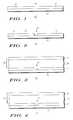
- FIGS. 1-7illustrate steps in the fabrication of a tiered structure, and more specifically a T-gate structure, according to the present invention. It should be understood that during the course of this description, like numbers are used to identify like elements according to the different figures that illustrate the invention. Accordingly, FIG. 1 illustrates in simplified cross-sectional view a first step in the method of fabricating a tiered structure according to the present invention. Illustrated in FIG. 1 is a first step in the fabrication of the semiconductor device of the present invention, generally referenced 10 , including the providing of a substrate 12 . Substrate 12 is described as being formed of a material chosen from the group consisting of: a column III-V compound semiconductor material, glass, metal, and silicon.
- substrate 12is described as being formed of an InP material. It should be understood, that anticipated by this disclosure is the fabrication of substrate 12 of an InGaAs material, a GaAs material, silicon, or any other materials commonly utilized in the fabrication of semiconductor devices.
- Substrate 12has disposed on an upper surface 13 , a base resist layer 14 , or first resist layer. It is disclosed that base resist layer 14 is formed of an organic, photosensitive or photoimageable material which is disposed on surface 13 of substrate 12 , using typical resist deposition techniques. More specifically, base resist layer 14 is deposited on surface 13 of substrate 12 using standard spin-coating techniques, thereby providing for base resist layer 14 to have a planarized uppermost surface 15 .
- base resist layer 14is disclosed as formed of a thin layer of an organic photosensitive material, such as novolak, or other similar material that is soluble and has a low molecular weight. It should be understood that anticipated by this disclosure is the fabrication of base resist layer 14 using a moderate or high molecular weight soluble material. According to this disclosure, low molecular weight materials include those materials having a molecular weight of less than 20,000. Medium molecular weight materials include those materials having a molecular weight of 20,000-200,000. High molecular weight materials include those materials having a molecular weight of more than 200,000. Base resist layer 14 in this particular embodiment is deposited at a thickness of less than 300 nm, preferably with a thickness of 150-300 nm, using standard spin coating techniques, well known in the industry.
- base resist layer 14is next developed as illustrated in FIG. 2, by imaging layer 14 with a light, electrons or other irradiating source, so as to form an opening 16 in resist layer 14 . Opening 16 provides for the fabrication of a gate stem (discussed presently).
- the remaining portions of base resist layer 14undergo a stabilization process in which base resist layer 14 is cross-linked by applying irradiating light and heat to layer 14 . It should be understood that additionally anticipated by this disclosure is the stabilization of base resist layer 14 by electron beam radiation combined with heat, by electron beam radiation alone, by irradiating light alone, or by heat alone.
- base resist layer 14undergoes a chemical reaction, causing the molecular weight of the material to increase, without destroying opening 16 , or more particularly the gate stem opening.
- Anticipatedis the use of irradiating light having wavelengths from 150 nm to 1000 nm. More specifically, the choice of wavelength depends upon the chemical structure of the base layer and is chosen so as to affect a cross-linking of base resist layer 14 .
- deep ultraviolet lighthaving a wavelength between 220-365 nm, is directed toward base resist layer 14 , during the stabilization process, although it is anticipated by this disclosure to extend this exposure to other wavelengths including broadband illumination.
- the intensity of the light, as well as the heat, and the time in which both must be applied to achieve cross-linking,is controllable so as to achieve maximum benefits.
- This process of photostabilizationprovides for a dramatic reduction of the solubility of base resist layer 14 in a solvent and results in a stabilized base resist layer 14 .
- resist stack 18is deposited on an uppermost surface 15 of stabilized base resist layer 14 .
- resist stack 18is deposited on surface 15 of stabilized base resist layer 14 by spin coating, or some other similar technique known in the art for depositing resist layers.
- resist stack 18is formed of multiple layers, consisting of one or more layers of photo-imageable organic resist layers, including those materials that are optically and/or electron beam sensitive. Illustrated in FIG. 3, is an organic resist stack 18 formed as a standard bilayer resist, including resist layers 20 and 22 . Illustrated in FIG. 4, in the alternative, is an organic resist stack 18 ′ formed as a standard single layer resist. It should be noted that all components of FIG. 4 that are similar to the components illustrated in FIG. 3, are designated with similar numbers, having a prime added to indicate the different embodiment.
- resist stack 18is formed of resist layer 20 that is more isotropically developing than stabilized base resist layer 14 or subsequent resist layer 22 .
- Resist layer 22is typically formed of a low molecular photoimageable material, similar to the material forming stabilized base resist layer 14 . Due to the stabilization of base resist layer 14 , there is no intermixing of materials, or deformation of stabilized base resist layer 14 with this subsequent deposition of resist layers 20 and 22 .
- organic resist stack 18 ′formed as a standard single layer resist, undergoes a diffusion step during processing. During this step, a chemical transformation of stack 18 ′ results in a bi-layer stack wherein a portion 20 ′ of resist stack 18 ′ formed nearer the surface of stabilized base resist layer 14 ′ is more isotropically developed and thus more soluble, than a portion 22 ′ of resist stack 18 ′ formed in the uppermost portion of the resist stack 18 ′. More specifically, during fabrication resist stack 18 ′ is immersed in an aqueous base solution, wherein the base within the developer diffuses into the uppermost portion 22 ′ of resist stack 18 ′.
- resist stack 18 ′This diffusion of the base into uppermost portion 22 ′ of resist stack 18 ′ results in a bi-layer resist including portion, or layer, 20 ′, which is similar to the initial base resist layer 14 prior to stabilization, and portion, or layer, 22 ′. It should be understood, that resist stack 18 ( 18 ′), irrespective of being formed as a single layer resist stack, or a multiple layer resist stack, is formed as a positive resist.
- wafer stack 10and more specifically, resist stack 18 , is next developed and patterned using standard lithographic methods, such as electron beam radiation, optical irradiation, or the like.
- standard lithographic methodssuch as electron beam radiation, optical irradiation, or the like.
- the exposed area of stack 18is removed, thereby defining an opening 24 and forming the pattern.
- an opening having a re-entrant profile 26is formed during development in resist layer 20 , due to the specific properties present in resist layer 20 . More specifically, negative sloping occurs to form sidewalls 28 in resist layer 20 , thereby forming the opening for the uppermost portion of the T which forms the T-gate structure.
- opening 24 formed to define the dimension of the uppermost portion of the tiered structurehas a preferred dimensional ratio of at least 2:1 with respect to opening 16 which forms the stem portion of the T-gate structure.
- opening 16has a dimension of approximately 250 nanometers microns
- opening 24has a dimension of approximately 750 nanometers.
- Opening 24is described as having a dimension that is less than opening 26 , but greater than opening 16 .
- metallizationtakes place whereby a conductive metal material 30 is deposited within openings 24 , 26 , and 16 , thereby forming a tiered structure 32 , and in this particular example, a T-gate structure, as illustrated in FIG. 6 .
- stack 10Prior to metallization, stack 10 is first soaked in a 10% NH 4 OH solution for a duration of typically 1 to 5 minutes. The soaking of stack 10 in the NH 4 OH solution provides for the cleaning of the exposed surfaces prior to metallization.
- Metallizationoccurs by evaporation of sputtering techniques, well known in the art. It is anticipated by this disclosure, that any type of conductive metal, such as gold (Au), titanium (Ti), or the like can be used during the metallization process to form tiered structure 32 .
- resist stack 18including resist layers 20 and 22 , and any metal 30 deposited on layer 22 during the metallization process, are removed.
- This step of removalmay be done by techniques including a solvent bath immersion to remove resist stack 18 , and dry oxygen plasma etching, or the like, to remove the stabilized base resist layer 14 .
- the resultis the fabrication of tiered structure 30 , and more particularly the T-gate structure, as illustrated.
- FIG. 8illustrated is a process of fabricating a semiconductor device 42 , including the step of fabricating a tiered structure 40 , generally similar to T-gate 32 of FIG. 7 .
- Semiconductor device 42 in this particular embodimentis formed as a transistor. It should be understood that while the manufacturing of a semiconductor device, and specifically a transistor, is described with respect to FIG. 8, that the manufacture of additional microelectronic devices that utilize tiered structures is anticipated by this disclosure.
- Semiconductor device, or transistor, 42is formed by initially providing a semiconductor substrate 44 .
- a source 46 and a drain 48are formed on an uppermost surface of the semiconductor substrate.
- Source 46 and drain 48 in this particular embodimentare formed as a layered structure, comprised of a semiconductor material, such as germanium (Ge), sandwiched between two metallic layers, such as nickel (Ni), and gold (Au). It should be understood that although these specific source and drain materials are disclosed, alternative materials commonly used for source and drain structures are intended to be included herein.
- a tiered structure 40such as a T-gate, is fabricated in accordance with the description given for FIGS. 1-7. Tiered structure 40 is positioned between source 46 and 48 to form complete semiconductor device, or transistor, 42 .
- a method for fabricating a tiered structuresuch as a T-gate structure, and a device in which the tiered structure is used, is disclosed.
- the tiered structureincludes an initially deposited resist layer that is stabilized, thereby providing for the subsequent deposition of a resist stack without deforming a stem opening formed in the stabilized layer.
- the inclusion of a stabilized resist layerprovides for subsequent resist layer deposition without interlayer intermixing. This enhancement of the resist properties provides for improved fabrication of semiconductor devices, including the ease with which subsequent deposition of resist layers is achieved.
Landscapes
- Engineering & Computer Science (AREA)
- Physics & Mathematics (AREA)
- Condensed Matter Physics & Semiconductors (AREA)
- General Physics & Mathematics (AREA)
- Manufacturing & Machinery (AREA)
- Computer Hardware Design (AREA)
- Microelectronics & Electronic Packaging (AREA)
- Power Engineering (AREA)
- Photosensitive Polymer And Photoresist Processing (AREA)
- Junction Field-Effect Transistors (AREA)
- Exposure Of Semiconductors, Excluding Electron Or Ion Beam Exposure (AREA)
Abstract
Description
Claims (24)
Priority Applications (4)
| Application Number | Priority Date | Filing Date | Title |
|---|---|---|---|
| US10/081,199US6737202B2 (en) | 2002-02-22 | 2002-02-22 | Method of fabricating a tiered structure using a multi-layered resist stack and use |
| PCT/US2003/003498WO2003073477A2 (en) | 2002-02-22 | 2003-02-04 | Tiered structure having a multi-layered resist stack |
| AU2003215061AAU2003215061A1 (en) | 2002-02-22 | 2003-02-04 | Tiered structure having a multi-layered resist stack |
| TW092103527ATWI274400B (en) | 2002-02-22 | 2003-02-20 | Method of fabricating a tiered structure using a multi-layered resist stack and use |
Applications Claiming Priority (1)
| Application Number | Priority Date | Filing Date | Title |
|---|---|---|---|
| US10/081,199US6737202B2 (en) | 2002-02-22 | 2002-02-22 | Method of fabricating a tiered structure using a multi-layered resist stack and use |
Publications (2)
| Publication Number | Publication Date |
|---|---|
| US20030162406A1 US20030162406A1 (en) | 2003-08-28 |
| US6737202B2true US6737202B2 (en) | 2004-05-18 |
Family
ID=27752923
Family Applications (1)
| Application Number | Title | Priority Date | Filing Date |
|---|---|---|---|
| US10/081,199Expired - LifetimeUS6737202B2 (en) | 2002-02-22 | 2002-02-22 | Method of fabricating a tiered structure using a multi-layered resist stack and use |
Country Status (4)
| Country | Link |
|---|---|
| US (1) | US6737202B2 (en) |
| AU (1) | AU2003215061A1 (en) |
| TW (1) | TWI274400B (en) |
| WO (1) | WO2003073477A2 (en) |
Cited By (46)
| Publication number | Priority date | Publication date | Assignee | Title |
|---|---|---|---|---|
| US20030215577A1 (en)* | 2002-05-16 | 2003-11-20 | Willson Carlton Grant | Method and system for fabricating nanoscale patterns in light curable compositions using an electric field |
| US20030235787A1 (en)* | 2002-06-24 | 2003-12-25 | Watts Michael P.C. | Low viscosity high resolution patterning material |
| US20040009673A1 (en)* | 2002-07-11 | 2004-01-15 | Sreenivasan Sidlgata V. | Method and system for imprint lithography using an electric field |
| US20040022888A1 (en)* | 2002-08-01 | 2004-02-05 | Sreenivasan Sidlgata V. | Alignment systems for imprint lithography |
| US20040038552A1 (en)* | 2002-08-23 | 2004-02-26 | Watts Michael P.C. | Method for fabricating bulbous-shaped vias |
| US20040053146A1 (en)* | 2000-07-16 | 2004-03-18 | University Of Texas System Board Of Regents, Ut System | Method of varying template dimensions to achieve alignment during imprint lithography |
| US20040104641A1 (en)* | 1999-10-29 | 2004-06-03 | University Of Texas System | Method of separating a template from a substrate during imprint lithography |
| US20040112153A1 (en)* | 2002-12-12 | 2004-06-17 | Molecular Imprints, Inc. | Method and system for determining characteristics of substrates employing fluid geometries |
| US20040112861A1 (en)* | 2002-12-11 | 2004-06-17 | Molecular Imprints, Inc. | Method for modulating shapes of substrates |
| US20040170770A1 (en)* | 2003-02-27 | 2004-09-02 | Molecular Imprints, Inc. | Method to reduce adhesion between a polymerizable layer and a substrate employing a fluorine-containing layer |
| US20040170771A1 (en)* | 2000-10-12 | 2004-09-02 | Board Of Regents, The University Of Texas System | Method of creating a dispersion of a liquid on a substrate |
| US20040188381A1 (en)* | 2003-03-25 | 2004-09-30 | Molecular Imprints, Inc. | Positive tone bi-layer imprint lithography method |
| US20040211754A1 (en)* | 2003-04-25 | 2004-10-28 | Molecular Imprints, Inc. | Method of forming stepped structures employing imprint lithography |
| US20050072755A1 (en)* | 2003-10-02 | 2005-04-07 | University Of Texas System Board Of Regents | Single phase fluid imprint lithography method |
| US6900881B2 (en) | 2002-07-11 | 2005-05-31 | Molecular Imprints, Inc. | Step and repeat imprint lithography systems |
| US6916584B2 (en) | 2002-08-01 | 2005-07-12 | Molecular Imprints, Inc. | Alignment methods for imprint lithography |
| US6926929B2 (en) | 2002-07-09 | 2005-08-09 | Molecular Imprints, Inc. | System and method for dispensing liquids |
| US6932934B2 (en) | 2002-07-11 | 2005-08-23 | Molecular Imprints, Inc. | Formation of discontinuous films during an imprint lithography process |
| US20060063112A1 (en)* | 2004-09-21 | 2006-03-23 | Molecular Imprints, Inc. | Pattern reversal employing thick residual layers |
| US20060063359A1 (en)* | 2004-09-21 | 2006-03-23 | Molecular Imprints, Inc. | Patterning substrates employing multi-film layers defining etch differential interfaces |
| US20060063387A1 (en)* | 2004-09-21 | 2006-03-23 | Molecular Imprints, Inc. | Method of Patterning Surfaces While Providing Greater Control of Recess Anisotropy |
| US20060063277A1 (en)* | 2004-09-21 | 2006-03-23 | Molecular Imprints, Inc. | Method of forming an in-situ recessed structure |
| US20060060557A1 (en)* | 2004-09-21 | 2006-03-23 | Sreenivasan Sidlgata V | Reverse tone patterning on surfaces having surface planarity perturbations |
| US7019819B2 (en) | 2002-11-13 | 2006-03-28 | Molecular Imprints, Inc. | Chucking system for modulating shapes of substrates |
| US7027156B2 (en) | 2002-08-01 | 2006-04-11 | Molecular Imprints, Inc. | Scatterometry alignment for imprint lithography |
| US7037639B2 (en) | 2002-05-01 | 2006-05-02 | Molecular Imprints, Inc. | Methods of manufacturing a lithography template |
| US20060113697A1 (en)* | 2004-12-01 | 2006-06-01 | Molecular Imprints, Inc. | Eliminating printability of sub-resolution defects in imprint lithography |
| US20060145398A1 (en)* | 2004-12-30 | 2006-07-06 | Board Of Regents, The University Of Texas System | Release layer comprising diamond-like carbon (DLC) or doped DLC with tunable composition for imprint lithography templates and contact masks |
| US7077992B2 (en) | 2002-07-11 | 2006-07-18 | Molecular Imprints, Inc. | Step and repeat imprint lithography processes |
| US20060228877A1 (en)* | 2005-04-07 | 2006-10-12 | Tdk Corporation | Patterned material layer, method of forming the same, microdevice, and method of manufacturing the same |
| US7122079B2 (en) | 2004-02-27 | 2006-10-17 | Molecular Imprints, Inc. | Composition for an etching mask comprising a silicon-containing material |
| US7136150B2 (en) | 2003-09-25 | 2006-11-14 | Molecular Imprints, Inc. | Imprint lithography template having opaque alignment marks |
| US7157036B2 (en) | 2003-06-17 | 2007-01-02 | Molecular Imprints, Inc | Method to reduce adhesion between a conformable region and a pattern of a mold |
| US20070017899A1 (en)* | 2005-07-19 | 2007-01-25 | Molecular Imprints, Inc. | Method of controlling the critical dimension of structures formed on a substrate |
| US20070048625A1 (en)* | 2005-08-26 | 2007-03-01 | Nordquist Kevin J | Lithographic template and method of formation and use |
| US7186656B2 (en) | 2004-05-21 | 2007-03-06 | Molecular Imprints, Inc. | Method of forming a recessed structure employing a reverse tone process |
| US20070077770A1 (en)* | 2005-09-30 | 2007-04-05 | Molecular Imprints, Inc. | Etching technique to planarize a multi-layer structure |
| US20080118872A1 (en)* | 2003-03-25 | 2008-05-22 | Molecular Imprints, Inc. | Positive Tone Bi-Layer Method |
| US20080141862A1 (en)* | 2003-10-02 | 2008-06-19 | Molecular Imprints, Inc. | Single Phase Fluid Imprint Lithography Method |
| US7439166B1 (en) | 2005-06-11 | 2008-10-21 | Hrl Laboratories, Llc | Method for producing tiered gate structure devices |
| US7608497B1 (en) | 2006-09-08 | 2009-10-27 | Ivan Milosavljevic | Passivated tiered gate structure transistor and fabrication method |
| US20100311242A1 (en)* | 2009-06-08 | 2010-12-09 | Globalfoundries Inc. | Methods for fabricating semiconductor devices |
| US8076386B2 (en) | 2004-02-23 | 2011-12-13 | Molecular Imprints, Inc. | Materials for imprint lithography |
| US8349241B2 (en) | 2002-10-04 | 2013-01-08 | Molecular Imprints, Inc. | Method to arrange features on a substrate to replicate features having minimal dimensional variability |
| US9223202B2 (en) | 2000-07-17 | 2015-12-29 | Board Of Regents, The University Of Texas System | Method of automatic fluid dispensing for imprint lithography processes |
| CN108807162A (en)* | 2018-05-28 | 2018-11-13 | 苏州汉骅半导体有限公司 | T-type grid preparation method |
Families Citing this family (10)
| Publication number | Priority date | Publication date | Assignee | Title |
|---|---|---|---|---|
| JP2003273131A (en)* | 2002-01-10 | 2003-09-26 | Murata Mfg Co Ltd | Masking member for forming fine electrode, method of manufacturing the same, method of forming the electrode, and field-effect transistor |
| US6852454B2 (en)* | 2002-06-18 | 2005-02-08 | Freescale Semiconductor, Inc. | Multi-tiered lithographic template and method of formation and use |
| US7435074B2 (en)* | 2004-03-13 | 2008-10-14 | International Business Machines Corporation | Method for fabricating dual damascence structures using photo-imprint lithography, methods for fabricating imprint lithography molds for dual damascene structures, materials for imprintable dielectrics and equipment for photo-imprint lithography used in dual damascence patterning |
| CN100372069C (en)* | 2004-05-19 | 2008-02-27 | 上海宏力半导体制造有限公司 | Method for forming T type polycrystalline silicon gate through double inlaying process |
| CN100369204C (en)* | 2004-05-19 | 2008-02-13 | 上海宏力半导体制造有限公司 | Method for manufacturing T-shaped polysilicon gate using dual damascene process |
| KR100620393B1 (en)* | 2005-11-03 | 2006-09-06 | 한국전자통신연구원 | Field effect transistor and its manufacturing method |
| US20080305442A1 (en)* | 2007-06-05 | 2008-12-11 | Tdk Corporation | Patterned material layer, method of forming the same, microdevice, and method of manufacturing the same |
| US8158014B2 (en)* | 2008-06-16 | 2012-04-17 | International Business Machines Corporation | Multi-exposure lithography employing differentially sensitive photoresist layers |
| CN102064104B (en)* | 2010-12-09 | 2011-12-28 | 中国电子科技集团公司第十三研究所 | Method for manufacturing T-shaped grid of GaN microwave device |
| US11387332B2 (en)* | 2018-06-27 | 2022-07-12 | Mitsubishi Electric Corporation | Method for manufacturing semiconductor device |
Citations (8)
| Publication number | Priority date | Publication date | Assignee | Title |
|---|---|---|---|---|
| EP0372790A2 (en) | 1988-11-28 | 1990-06-13 | Matsushita Electric Industrial Co., Ltd. | Developing solution and pattern forming method using same |
| US4975382A (en) | 1989-05-15 | 1990-12-04 | Rohm Co., Ltd. | Method of making a self-aligned field-effect transistor by the use of a dummy-gate |
| US5338703A (en)* | 1992-10-26 | 1994-08-16 | Mitsubishi Denki Kabushiki Kaisha | Method for producing a recessed gate field effect transistor |
| JPH07201889A (en)* | 1993-12-10 | 1995-08-04 | Korea Electron Telecommun | Method of manufacturing T-shaped gate by double exposure |
| JPH11150129A (en) | 1997-09-11 | 1999-06-02 | Matsushita Electric Ind Co Ltd | Semiconductor device and method of manufacturing semiconductor device |
| US5981319A (en)* | 1997-09-22 | 1999-11-09 | Lucent Technologies Inc. | Method of forming a T-shaped gate |
| US6051454A (en) | 1997-09-11 | 2000-04-18 | Matsushita Electric Industrial Co., Ltd. | Semiconductor device and method for fabricating the same |
| US6387783B1 (en)* | 1999-04-26 | 2002-05-14 | International Business Machines Corporation | Methods of T-gate fabrication using a hybrid resist |
- 2002
- 2002-02-22USUS10/081,199patent/US6737202B2/ennot_activeExpired - Lifetime
- 2003
- 2003-02-04WOPCT/US2003/003498patent/WO2003073477A2/ennot_activeApplication Discontinuation
- 2003-02-04AUAU2003215061Apatent/AU2003215061A1/ennot_activeAbandoned
- 2003-02-20TWTW092103527Apatent/TWI274400B/ennot_activeIP Right Cessation
Patent Citations (9)
| Publication number | Priority date | Publication date | Assignee | Title |
|---|---|---|---|---|
| EP0372790A2 (en) | 1988-11-28 | 1990-06-13 | Matsushita Electric Industrial Co., Ltd. | Developing solution and pattern forming method using same |
| US5122387A (en)* | 1988-11-28 | 1992-06-16 | Matsushita Electronics Corporation | Developing solution and pattern forming method using the same |
| US4975382A (en) | 1989-05-15 | 1990-12-04 | Rohm Co., Ltd. | Method of making a self-aligned field-effect transistor by the use of a dummy-gate |
| US5338703A (en)* | 1992-10-26 | 1994-08-16 | Mitsubishi Denki Kabushiki Kaisha | Method for producing a recessed gate field effect transistor |
| JPH07201889A (en)* | 1993-12-10 | 1995-08-04 | Korea Electron Telecommun | Method of manufacturing T-shaped gate by double exposure |
| JPH11150129A (en) | 1997-09-11 | 1999-06-02 | Matsushita Electric Ind Co Ltd | Semiconductor device and method of manufacturing semiconductor device |
| US6051454A (en) | 1997-09-11 | 2000-04-18 | Matsushita Electric Industrial Co., Ltd. | Semiconductor device and method for fabricating the same |
| US5981319A (en)* | 1997-09-22 | 1999-11-09 | Lucent Technologies Inc. | Method of forming a T-shaped gate |
| US6387783B1 (en)* | 1999-04-26 | 2002-05-14 | International Business Machines Corporation | Methods of T-gate fabrication using a hybrid resist |
Cited By (85)
| Publication number | Priority date | Publication date | Assignee | Title |
|---|---|---|---|---|
| US20040104641A1 (en)* | 1999-10-29 | 2004-06-03 | University Of Texas System | Method of separating a template from a substrate during imprint lithography |
| US20040168588A1 (en)* | 1999-10-29 | 2004-09-02 | Board Of Regents, The University Of Texas System | Method of orientating a template with respect to a substrate in response to a force exerted on the template |
| US7098572B2 (en) | 1999-10-29 | 2006-08-29 | Board Of Regents, The University Of Texas System | Apparatus to control displacement of a body spaced-apart from a surface |
| US7060402B2 (en) | 1999-10-29 | 2006-06-13 | Board Of Regents, The University Of Texas System | Method of orientating a template with respect to a substrate in response to a force exerted on the template |
| US20050089774A1 (en)* | 1999-10-29 | 2005-04-28 | Board Of Regents, The University Of Texas System | Method to control the relative position between a body and a surface |
| US6955868B2 (en) | 1999-10-29 | 2005-10-18 | Board Of Regents, The University Of Texas System | Method to control the relative position between a body and a surface |
| US6986975B2 (en) | 2000-07-16 | 2006-01-17 | Board Of Regents, The University Of Texas System | Method of aligning a template with a substrate employing moire patterns |
| US6919152B2 (en) | 2000-07-16 | 2005-07-19 | Board Of Regents, The University Of Texas System | High resolution overlay alignment systems for imprint lithography |
| US6842229B2 (en) | 2000-07-16 | 2005-01-11 | Board Of Regents, The University Of Texas System | Imprint lithography template comprising alignment marks |
| US20040053146A1 (en)* | 2000-07-16 | 2004-03-18 | University Of Texas System Board Of Regents, Ut System | Method of varying template dimensions to achieve alignment during imprint lithography |
| US6916585B2 (en) | 2000-07-16 | 2005-07-12 | Board Of Regents, The University Of Texas Systems | Method of varying template dimensions to achieve alignment during imprint lithography |
| US6902853B2 (en) | 2000-07-16 | 2005-06-07 | Board Of Regents, The University Of Texas System | Dual wavelength method of determining a relative position of a substrate and a template |
| US20040209177A1 (en)* | 2000-07-16 | 2004-10-21 | Board Of Regents, The University Of Texas System | Dual wavelength method of determining a relative position of a substrate and a template |
| US6921615B2 (en) | 2000-07-16 | 2005-07-26 | Board Of Regents, The University Of Texas System | High-resolution overlay alignment methods for imprint lithography |
| US9223202B2 (en) | 2000-07-17 | 2015-12-29 | Board Of Regents, The University Of Texas System | Method of automatic fluid dispensing for imprint lithography processes |
| US7060324B2 (en) | 2000-10-12 | 2006-06-13 | Board Of Regents, The University Of Texas System | Method of creating a dispersion of a liquid on a substrate |
| US20040170771A1 (en)* | 2000-10-12 | 2004-09-02 | Board Of Regents, The University Of Texas System | Method of creating a dispersion of a liquid on a substrate |
| US7037639B2 (en) | 2002-05-01 | 2006-05-02 | Molecular Imprints, Inc. | Methods of manufacturing a lithography template |
| US6964793B2 (en) | 2002-05-16 | 2005-11-15 | Board Of Regents, The University Of Texas System | Method for fabricating nanoscale patterns in light curable compositions using an electric field |
| US20030215577A1 (en)* | 2002-05-16 | 2003-11-20 | Willson Carlton Grant | Method and system for fabricating nanoscale patterns in light curable compositions using an electric field |
| US20030235787A1 (en)* | 2002-06-24 | 2003-12-25 | Watts Michael P.C. | Low viscosity high resolution patterning material |
| US6926929B2 (en) | 2002-07-09 | 2005-08-09 | Molecular Imprints, Inc. | System and method for dispensing liquids |
| US6932934B2 (en) | 2002-07-11 | 2005-08-23 | Molecular Imprints, Inc. | Formation of discontinuous films during an imprint lithography process |
| US20040009673A1 (en)* | 2002-07-11 | 2004-01-15 | Sreenivasan Sidlgata V. | Method and system for imprint lithography using an electric field |
| US7077992B2 (en) | 2002-07-11 | 2006-07-18 | Molecular Imprints, Inc. | Step and repeat imprint lithography processes |
| US6900881B2 (en) | 2002-07-11 | 2005-05-31 | Molecular Imprints, Inc. | Step and repeat imprint lithography systems |
| US6908861B2 (en) | 2002-07-11 | 2005-06-21 | Molecular Imprints, Inc. | Method for imprint lithography using an electric field |
| US20040022888A1 (en)* | 2002-08-01 | 2004-02-05 | Sreenivasan Sidlgata V. | Alignment systems for imprint lithography |
| US7070405B2 (en) | 2002-08-01 | 2006-07-04 | Molecular Imprints, Inc. | Alignment systems for imprint lithography |
| US6916584B2 (en) | 2002-08-01 | 2005-07-12 | Molecular Imprints, Inc. | Alignment methods for imprint lithography |
| US7027156B2 (en) | 2002-08-01 | 2006-04-11 | Molecular Imprints, Inc. | Scatterometry alignment for imprint lithography |
| US20040038552A1 (en)* | 2002-08-23 | 2004-02-26 | Watts Michael P.C. | Method for fabricating bulbous-shaped vias |
| US7071088B2 (en) | 2002-08-23 | 2006-07-04 | Molecular Imprints, Inc. | Method for fabricating bulbous-shaped vias |
| US8349241B2 (en) | 2002-10-04 | 2013-01-08 | Molecular Imprints, Inc. | Method to arrange features on a substrate to replicate features having minimal dimensional variability |
| US7019819B2 (en) | 2002-11-13 | 2006-03-28 | Molecular Imprints, Inc. | Chucking system for modulating shapes of substrates |
| US20040112861A1 (en)* | 2002-12-11 | 2004-06-17 | Molecular Imprints, Inc. | Method for modulating shapes of substrates |
| US6980282B2 (en) | 2002-12-11 | 2005-12-27 | Molecular Imprints, Inc. | Method for modulating shapes of substrates |
| US6871558B2 (en) | 2002-12-12 | 2005-03-29 | Molecular Imprints, Inc. | Method for determining characteristics of substrate employing fluid geometries |
| US20040112153A1 (en)* | 2002-12-12 | 2004-06-17 | Molecular Imprints, Inc. | Method and system for determining characteristics of substrates employing fluid geometries |
| US20040170770A1 (en)* | 2003-02-27 | 2004-09-02 | Molecular Imprints, Inc. | Method to reduce adhesion between a polymerizable layer and a substrate employing a fluorine-containing layer |
| US7452574B2 (en) | 2003-02-27 | 2008-11-18 | Molecular Imprints, Inc. | Method to reduce adhesion between a polymerizable layer and a substrate employing a fluorine-containing layer |
| US20080118872A1 (en)* | 2003-03-25 | 2008-05-22 | Molecular Imprints, Inc. | Positive Tone Bi-Layer Method |
| US7179396B2 (en) | 2003-03-25 | 2007-02-20 | Molecular Imprints, Inc. | Positive tone bi-layer imprint lithography method |
| US7670953B2 (en) | 2003-03-25 | 2010-03-02 | Molecular Imprints, Inc. | Positive tone bi-layer method |
| US20040188381A1 (en)* | 2003-03-25 | 2004-09-30 | Molecular Imprints, Inc. | Positive tone bi-layer imprint lithography method |
| US7396475B2 (en) | 2003-04-25 | 2008-07-08 | Molecular Imprints, Inc. | Method of forming stepped structures employing imprint lithography |
| US20040211754A1 (en)* | 2003-04-25 | 2004-10-28 | Molecular Imprints, Inc. | Method of forming stepped structures employing imprint lithography |
| US7157036B2 (en) | 2003-06-17 | 2007-01-02 | Molecular Imprints, Inc | Method to reduce adhesion between a conformable region and a pattern of a mold |
| US7136150B2 (en) | 2003-09-25 | 2006-11-14 | Molecular Imprints, Inc. | Imprint lithography template having opaque alignment marks |
| US20080141862A1 (en)* | 2003-10-02 | 2008-06-19 | Molecular Imprints, Inc. | Single Phase Fluid Imprint Lithography Method |
| US20050072755A1 (en)* | 2003-10-02 | 2005-04-07 | University Of Texas System Board Of Regents | Single phase fluid imprint lithography method |
| US7090716B2 (en) | 2003-10-02 | 2006-08-15 | Molecular Imprints, Inc. | Single phase fluid imprint lithography method |
| US8211214B2 (en) | 2003-10-02 | 2012-07-03 | Molecular Imprints, Inc. | Single phase fluid imprint lithography method |
| US8076386B2 (en) | 2004-02-23 | 2011-12-13 | Molecular Imprints, Inc. | Materials for imprint lithography |
| US7122079B2 (en) | 2004-02-27 | 2006-10-17 | Molecular Imprints, Inc. | Composition for an etching mask comprising a silicon-containing material |
| US7186656B2 (en) | 2004-05-21 | 2007-03-06 | Molecular Imprints, Inc. | Method of forming a recessed structure employing a reverse tone process |
| US20060063277A1 (en)* | 2004-09-21 | 2006-03-23 | Molecular Imprints, Inc. | Method of forming an in-situ recessed structure |
| US7041604B2 (en) | 2004-09-21 | 2006-05-09 | Molecular Imprints, Inc. | Method of patterning surfaces while providing greater control of recess anisotropy |
| US20060063359A1 (en)* | 2004-09-21 | 2006-03-23 | Molecular Imprints, Inc. | Patterning substrates employing multi-film layers defining etch differential interfaces |
| US7205244B2 (en) | 2004-09-21 | 2007-04-17 | Molecular Imprints | Patterning substrates employing multi-film layers defining etch-differential interfaces |
| US7241395B2 (en) | 2004-09-21 | 2007-07-10 | Molecular Imprints, Inc. | Reverse tone patterning on surfaces having planarity perturbations |
| US7252777B2 (en) | 2004-09-21 | 2007-08-07 | Molecular Imprints, Inc. | Method of forming an in-situ recessed structure |
| US20060063387A1 (en)* | 2004-09-21 | 2006-03-23 | Molecular Imprints, Inc. | Method of Patterning Surfaces While Providing Greater Control of Recess Anisotropy |
| US20060060557A1 (en)* | 2004-09-21 | 2006-03-23 | Sreenivasan Sidlgata V | Reverse tone patterning on surfaces having surface planarity perturbations |
| US20060063112A1 (en)* | 2004-09-21 | 2006-03-23 | Molecular Imprints, Inc. | Pattern reversal employing thick residual layers |
| US7547504B2 (en) | 2004-09-21 | 2009-06-16 | Molecular Imprints, Inc. | Pattern reversal employing thick residual layers |
| US7357876B2 (en) | 2004-12-01 | 2008-04-15 | Molecular Imprints, Inc. | Eliminating printability of sub-resolution defects in imprint lithography |
| US20060113697A1 (en)* | 2004-12-01 | 2006-06-01 | Molecular Imprints, Inc. | Eliminating printability of sub-resolution defects in imprint lithography |
| US20060145398A1 (en)* | 2004-12-30 | 2006-07-06 | Board Of Regents, The University Of Texas System | Release layer comprising diamond-like carbon (DLC) or doped DLC with tunable composition for imprint lithography templates and contact masks |
| US20060228877A1 (en)* | 2005-04-07 | 2006-10-12 | Tdk Corporation | Patterned material layer, method of forming the same, microdevice, and method of manufacturing the same |
| US7700482B2 (en)* | 2005-04-07 | 2010-04-20 | Tdk Corporation | Patterned material layer, method of forming the same, microdevice, and method of manufacturing the same |
| US7439166B1 (en) | 2005-06-11 | 2008-10-21 | Hrl Laboratories, Llc | Method for producing tiered gate structure devices |
| US7723761B1 (en) | 2005-06-11 | 2010-05-25 | Hrl Laboratories, Llc | Tiered gate structure devices |
| US7256131B2 (en) | 2005-07-19 | 2007-08-14 | Molecular Imprints, Inc. | Method of controlling the critical dimension of structures formed on a substrate |
| US20070017899A1 (en)* | 2005-07-19 | 2007-01-25 | Molecular Imprints, Inc. | Method of controlling the critical dimension of structures formed on a substrate |
| US7425392B2 (en) | 2005-08-26 | 2008-09-16 | Motorola, Inc. | Lithographic template and method of formation and use |
| US20070048625A1 (en)* | 2005-08-26 | 2007-03-01 | Nordquist Kevin J | Lithographic template and method of formation and use |
| US7259102B2 (en) | 2005-09-30 | 2007-08-21 | Molecular Imprints, Inc. | Etching technique to planarize a multi-layer structure |
| US20070077770A1 (en)* | 2005-09-30 | 2007-04-05 | Molecular Imprints, Inc. | Etching technique to planarize a multi-layer structure |
| US7608497B1 (en) | 2006-09-08 | 2009-10-27 | Ivan Milosavljevic | Passivated tiered gate structure transistor and fabrication method |
| US8039903B1 (en) | 2006-09-08 | 2011-10-18 | Hrl Laboratories, Llc | Passivated tiered gate structure transistor |
| US20100311242A1 (en)* | 2009-06-08 | 2010-12-09 | Globalfoundries Inc. | Methods for fabricating semiconductor devices |
| US8361335B2 (en) | 2009-06-08 | 2013-01-29 | GlobalFoundries, Inc. | Methods for fabricating semiconductor devices |
| US8637214B2 (en) | 2009-06-08 | 2014-01-28 | GlobalFoundries, Inc. | Photomask sets for fabricating semiconductor devices |
| CN108807162A (en)* | 2018-05-28 | 2018-11-13 | 苏州汉骅半导体有限公司 | T-type grid preparation method |
Also Published As
| Publication number | Publication date |
|---|---|
| TW200305975A (en) | 2003-11-01 |
| WO2003073477A2 (en) | 2003-09-04 |
| AU2003215061A8 (en) | 2003-09-09 |
| WO2003073477A3 (en) | 2003-12-31 |
| TWI274400B (en) | 2007-02-21 |
| AU2003215061A1 (en) | 2003-09-09 |
| US20030162406A1 (en) | 2003-08-28 |
Similar Documents
| Publication | Publication Date | Title |
|---|---|---|
| US6737202B2 (en) | Method of fabricating a tiered structure using a multi-layered resist stack and use | |
| CN104882373B (en) | The manufacture method of transistor T-shaped grid | |
| US5147740A (en) | Structure and process for fabricating conductive patterns having sub-half micron dimensions | |
| US6387783B1 (en) | Methods of T-gate fabrication using a hybrid resist | |
| KR101125707B1 (en) | T-gate formation | |
| US5804474A (en) | Method for forming a V-shaped gate electrode in a semiconductor device, and the structure of the electrode | |
| US4959326A (en) | Fabricating T-gate MESFETS employing double exposure, double develop techniques | |
| JPH0620062B2 (en) | Method for manufacturing semiconductor device | |
| US5700628A (en) | Dry microlithography process | |
| US6767693B1 (en) | Materials and methods for sub-lithographic patterning of contact, via, and trench structures in integrated circuit devices | |
| KR100581450B1 (en) | Improved deep ultra violet photolithography | |
| US6420271B2 (en) | Method of forming a pattern | |
| US6933247B2 (en) | Method for forming a minute pattern and method for manufacturing a semiconductor device using the same | |
| CN108231548A (en) | Method for manufacturing semiconductor device | |
| US6589709B1 (en) | Process for preventing deformation of patterned photoresist features | |
| US5876901A (en) | Method for fabricating semiconductor device | |
| TWI254992B (en) | Method of fabricating a vertically profiled electrode and semiconductor device comprising such an electrode | |
| US6977219B2 (en) | Solvent vapor-assisted plasticization of photoresist films to achieve critical dimension reduction during temperature reflow | |
| US9443740B1 (en) | Process for forming gate of thin film transistor devices | |
| US6884735B1 (en) | Materials and methods for sublithographic patterning of gate structures in integrated circuit devices | |
| KR20230022951A (en) | Methods for Forming Narrow Slot Contacts | |
| JP2610402B2 (en) | Method of manufacturing T-shaped gate by double exposure | |
| US7625822B2 (en) | Semiconductor device and method for manufacturing the same including two antireflective coating films | |
| US10863630B2 (en) | Material composition and methods thereof | |
| EP1708253B1 (en) | Semiconductor device fabrication method |
Legal Events
| Date | Code | Title | Description |
|---|---|---|---|
| AS | Assignment | Owner name:MOTOROLA, INC., ILLINOIS Free format text:ASSIGNMENT OF ASSIGNORS INTEREST;ASSIGNORS:GEHOSKI, KATHLEEN ANN;POPOVICH, LAURA;MANCINI, DAVID P.;AND OTHERS;REEL/FRAME:012654/0954 Effective date:20020221 | |
| STCF | Information on status: patent grant | Free format text:PATENTED CASE | |
| AS | Assignment | Owner name:FREESCALE SEMICONDUCTOR, INC., TEXAS Free format text:ASSIGNMENT OF ASSIGNORS INTEREST;ASSIGNOR:MOTOROLA, INC;REEL/FRAME:015360/0718 Effective date:20040404 Owner name:FREESCALE SEMICONDUCTOR, INC.,TEXAS Free format text:ASSIGNMENT OF ASSIGNORS INTEREST;ASSIGNOR:MOTOROLA, INC;REEL/FRAME:015360/0718 Effective date:20040404 | |
| AS | Assignment | Owner name:CITIBANK, N.A. AS COLLATERAL AGENT, NEW YORK Free format text:SECURITY AGREEMENT;ASSIGNORS:FREESCALE SEMICONDUCTOR, INC.;FREESCALE ACQUISITION CORPORATION;FREESCALE ACQUISITION HOLDINGS CORP.;AND OTHERS;REEL/FRAME:018855/0129 Effective date:20061201 Owner name:CITIBANK, N.A. AS COLLATERAL AGENT,NEW YORK Free format text:SECURITY AGREEMENT;ASSIGNORS:FREESCALE SEMICONDUCTOR, INC.;FREESCALE ACQUISITION CORPORATION;FREESCALE ACQUISITION HOLDINGS CORP.;AND OTHERS;REEL/FRAME:018855/0129 Effective date:20061201 | |
| FPAY | Fee payment | Year of fee payment:4 | |
| AS | Assignment | Owner name:NATIONAL INSTITUTES OF HEALTH (NIH), U.S. DEPT. OF Free format text:EXECUTIVE ORDER 9424, CONFIRMATORY LICENSE;ASSIGNOR:THE PENNSYLVANIA STATE UNIVERSITY;REEL/FRAME:021743/0296 Effective date:20000809 | |
| AS | Assignment | Owner name:CITIBANK, N.A., AS COLLATERAL AGENT,NEW YORK Free format text:SECURITY AGREEMENT;ASSIGNOR:FREESCALE SEMICONDUCTOR, INC.;REEL/FRAME:024397/0001 Effective date:20100413 Owner name:CITIBANK, N.A., AS COLLATERAL AGENT, NEW YORK Free format text:SECURITY AGREEMENT;ASSIGNOR:FREESCALE SEMICONDUCTOR, INC.;REEL/FRAME:024397/0001 Effective date:20100413 | |
| FPAY | Fee payment | Year of fee payment:8 | |
| AS | Assignment | Owner name:CITIBANK, N.A., AS NOTES COLLATERAL AGENT, NEW YORK Free format text:SECURITY AGREEMENT;ASSIGNOR:FREESCALE SEMICONDUCTOR, INC.;REEL/FRAME:030633/0424 Effective date:20130521 Owner name:CITIBANK, N.A., AS NOTES COLLATERAL AGENT, NEW YOR Free format text:SECURITY AGREEMENT;ASSIGNOR:FREESCALE SEMICONDUCTOR, INC.;REEL/FRAME:030633/0424 Effective date:20130521 | |
| AS | Assignment | Owner name:CITIBANK, N.A., AS NOTES COLLATERAL AGENT, NEW YORK Free format text:SECURITY AGREEMENT;ASSIGNOR:FREESCALE SEMICONDUCTOR, INC.;REEL/FRAME:031591/0266 Effective date:20131101 Owner name:CITIBANK, N.A., AS NOTES COLLATERAL AGENT, NEW YOR Free format text:SECURITY AGREEMENT;ASSIGNOR:FREESCALE SEMICONDUCTOR, INC.;REEL/FRAME:031591/0266 Effective date:20131101 | |
| FPAY | Fee payment | Year of fee payment:12 | |
| AS | Assignment | Owner name:FREESCALE SEMICONDUCTOR, INC., TEXAS Free format text:PATENT RELEASE;ASSIGNOR:CITIBANK, N.A., AS COLLATERAL AGENT;REEL/FRAME:037354/0225 Effective date:20151207 Owner name:FREESCALE SEMICONDUCTOR, INC., TEXAS Free format text:PATENT RELEASE;ASSIGNOR:CITIBANK, N.A., AS COLLATERAL AGENT;REEL/FRAME:037356/0553 Effective date:20151207 Owner name:FREESCALE SEMICONDUCTOR, INC., TEXAS Free format text:PATENT RELEASE;ASSIGNOR:CITIBANK, N.A., AS COLLATERAL AGENT;REEL/FRAME:037356/0143 Effective date:20151207 | |
| AS | Assignment | Owner name:MORGAN STANLEY SENIOR FUNDING, INC., MARYLAND Free format text:ASSIGNMENT AND ASSUMPTION OF SECURITY INTEREST IN PATENTS;ASSIGNOR:CITIBANK, N.A.;REEL/FRAME:037486/0517 Effective date:20151207 | |
| AS | Assignment | Owner name:MORGAN STANLEY SENIOR FUNDING, INC., MARYLAND Free format text:ASSIGNMENT AND ASSUMPTION OF SECURITY INTEREST IN PATENTS;ASSIGNOR:CITIBANK, N.A.;REEL/FRAME:037518/0292 Effective date:20151207 | |
| AS | Assignment | Owner name:MORGAN STANLEY SENIOR FUNDING, INC., MARYLAND Free format text:SUPPLEMENT TO THE SECURITY AGREEMENT;ASSIGNOR:FREESCALE SEMICONDUCTOR, INC.;REEL/FRAME:039138/0001 Effective date:20160525 | |
| AS | Assignment | Owner name:NXP, B.V., F/K/A FREESCALE SEMICONDUCTOR, INC., NETHERLANDS Free format text:RELEASE BY SECURED PARTY;ASSIGNOR:MORGAN STANLEY SENIOR FUNDING, INC.;REEL/FRAME:040925/0001 Effective date:20160912 Owner name:NXP, B.V., F/K/A FREESCALE SEMICONDUCTOR, INC., NE Free format text:RELEASE BY SECURED PARTY;ASSIGNOR:MORGAN STANLEY SENIOR FUNDING, INC.;REEL/FRAME:040925/0001 Effective date:20160912 | |
| AS | Assignment | Owner name:NXP B.V., NETHERLANDS Free format text:RELEASE BY SECURED PARTY;ASSIGNOR:MORGAN STANLEY SENIOR FUNDING, INC.;REEL/FRAME:040928/0001 Effective date:20160622 | |
| AS | Assignment | Owner name:NXP USA, INC., TEXAS Free format text:MERGER;ASSIGNOR:FREESCALE SEMICONDUCTOR, INC.;REEL/FRAME:041144/0363 Effective date:20161107 | |
| AS | Assignment | Owner name:MORGAN STANLEY SENIOR FUNDING, INC., MARYLAND Free format text:CORRECTIVE ASSIGNMENT TO CORRECT THE REMOVE PATENTS 8108266 AND 8062324 AND REPLACE THEM WITH 6108266 AND 8060324 PREVIOUSLY RECORDED ON REEL 037518 FRAME 0292. ASSIGNOR(S) HEREBY CONFIRMS THE ASSIGNMENT AND ASSUMPTION OF SECURITY INTEREST IN PATENTS;ASSIGNOR:CITIBANK, N.A.;REEL/FRAME:041703/0536 Effective date:20151207 | |
| AS | Assignment | Owner name:SHENZHEN XINGUODU TECHNOLOGY CO., LTD., CHINA Free format text:CORRECTIVE ASSIGNMENT TO CORRECT THE TO CORRECT THE APPLICATION NO. FROM 13,883,290 TO 13,833,290 PREVIOUSLY RECORDED ON REEL 041703 FRAME 0536. ASSIGNOR(S) HEREBY CONFIRMS THE THE ASSIGNMENT AND ASSUMPTION OF SECURITYINTEREST IN PATENTS.;ASSIGNOR:MORGAN STANLEY SENIOR FUNDING, INC.;REEL/FRAME:048734/0001 Effective date:20190217 | |
| AS | Assignment | Owner name:NXP B.V., NETHERLANDS Free format text:RELEASE BY SECURED PARTY;ASSIGNOR:MORGAN STANLEY SENIOR FUNDING, INC.;REEL/FRAME:050744/0097 Effective date:20190903 | |
| AS | Assignment | Owner name:MORGAN STANLEY SENIOR FUNDING, INC., MARYLAND Free format text:CORRECTIVE ASSIGNMENT TO CORRECT THE REMOVE APPLICATION11759915 AND REPLACE IT WITH APPLICATION 11759935 PREVIOUSLY RECORDED ON REEL 037486 FRAME 0517. ASSIGNOR(S) HEREBY CONFIRMS THE ASSIGNMENT AND ASSUMPTION OF SECURITYINTEREST IN PATENTS;ASSIGNOR:CITIBANK, N.A.;REEL/FRAME:053547/0421 Effective date:20151207 | |
| AS | Assignment | Owner name:NXP B.V., NETHERLANDS Free format text:CORRECTIVE ASSIGNMENT TO CORRECT THE REMOVEAPPLICATION 11759915 AND REPLACE IT WITH APPLICATION11759935 PREVIOUSLY RECORDED ON REEL 040928 FRAME 0001. ASSIGNOR(S) HEREBY CONFIRMS THE RELEASE OF SECURITYINTEREST;ASSIGNOR:MORGAN STANLEY SENIOR FUNDING, INC.;REEL/FRAME:052915/0001 Effective date:20160622 | |
| AS | Assignment | Owner name:NXP, B.V. F/K/A FREESCALE SEMICONDUCTOR, INC., NETHERLANDS Free format text:CORRECTIVE ASSIGNMENT TO CORRECT THE REMOVEAPPLICATION 11759915 AND REPLACE IT WITH APPLICATION11759935 PREVIOUSLY RECORDED ON REEL 040925 FRAME 0001. ASSIGNOR(S) HEREBY CONFIRMS THE RELEASE OF SECURITYINTEREST;ASSIGNOR:MORGAN STANLEY SENIOR FUNDING, INC.;REEL/FRAME:052917/0001 Effective date:20160912 |