US6735546B2 - Memory device and method for temperature-based control over write and/or read operations - Google Patents
Memory device and method for temperature-based control over write and/or read operationsDownload PDFInfo
- Publication number
- US6735546B2 US6735546B2US09/944,613US94461301AUS6735546B2US 6735546 B2US6735546 B2US 6735546B2US 94461301 AUS94461301 AUS 94461301AUS 6735546 B2US6735546 B2US 6735546B2
- Authority
- US
- United States
- Prior art keywords
- temperature
- memory array
- read operation
- temperature sensor
- write
- Prior art date
- Legal status (The legal status is an assumption and is not a legal conclusion. Google has not performed a legal analysis and makes no representation as to the accuracy of the status listed.)
- Expired - Lifetime
Links
Images


Classifications
- G—PHYSICS
- G11—INFORMATION STORAGE
- G11C—STATIC STORES
- G11C7/00—Arrangements for writing information into, or reading information out from, a digital store
- G11C7/04—Arrangements for writing information into, or reading information out from, a digital store with means for avoiding disturbances due to temperature effects
- G—PHYSICS
- G01—MEASURING; TESTING
- G01K—MEASURING TEMPERATURE; MEASURING QUANTITY OF HEAT; THERMALLY-SENSITIVE ELEMENTS NOT OTHERWISE PROVIDED FOR
- G01K3/00—Thermometers giving results other than momentary value of temperature
- G01K3/005—Circuits arrangements for indicating a predetermined temperature
Definitions
- Passive element memory arrayssuch as anti-fuse diode cell arrays, require a high-voltage and high-current programming voltage source due to the large number of leakage paths in the array and the high voltage required to program the element conductivity.
- the write power dissipationis dominated by the power of the programming voltage source, and the write power increases the temperature of the memory.
- the temperature of the diodesincreases, the diode leakage current and the write power further increase, and this feedback can cause thermal run-away and failure of the memory.
- the memorycan be designed with smaller sub-arrays and a lower data rate. However, this design increases the cost per unit of storage capacity and results in a relatively slow memory device.
- the preferred embodiments described belowprovide a memory device and method for temperature-based control over write and/or read operations.
- the temperature of a memory arrayis monitored, and a write operation to the memory array is prevented in response to the monitored temperature reaching a threshold temperature.
- the temperature of a memory arrayis monitored, and a read operation from the memory array is prevented in response to the monitored temperature reaching a threshold temperature.
- Other preferred embodimentsare provided, and each of the preferred embodiments can be used alone or in combination with one another.
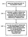
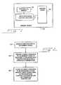
- FIG. 1is an illustration of a memory device of a preferred embodiment having a temperature sensor and write operation control circuitry.
- FIG. 2is a flow chart of a method of a preferred embodiment for temperature-based control of a write operation.
- FIG. 3Ais a graph showing a distribution of memory arrays versus temperature.
- FIG. 3Bis a graph showing a distribution of memory arrays with write operation control circuitry of a preferred embodiment versus temperature.
- FIG. 4is an illustration of a circuit of a preferred embodiment for temperature-based control of a write operation.
- FIG. 5is an illustration of a circuit of a preferred embodiment for temperature-based control of a read operation.
- FIG. 1is an illustration of a memory device 100 of a preferred embodiment.
- the memory device 100comprises write operation control circuitry 110 coupled with a temperature sensor 120 and a memory array 130 .
- the terms “coupled with” and “connected to”are intended broadly to cover elements that are coupled with or connected to one another either directly or indirectly through one or more intervening components.
- the memory device 100implements a method for temperature-based control of a write operation, which is illustrated in the flow chart of FIG. 2 .
- the temperature of the memory array 130is monitored (act 210 ).
- the temperature of the memory array 130can be monitored directly or indirectly.
- the temperature sensor 120can be located on the same substrate that supports the memory array 130 (an “on-chip” temperature sensor), or the temperature sensor 120 can be located on another component housed by the housing of the memory device, such as interface circuitry (an “off-chip” temperature sensor).
- a write operation to the memory array 130is prevented in response to the monitored temperature reaching a threshold temperature (act 220 ).
- the monitored temperature“reaches” the threshold temperature when the monitored temperature is at or above the threshold temperature.
- the term “reach”is also intended to cover the situation in which the monitored temperature is “reached” only when the monitored temperature is above (but not at) the threshold temperature.
- the write operation that was previously preventedis allowed to be performed to the memory array (act 230 ).
- an actionis performed “in response to” an event when that action is performed immediately after the event or at some time after the event (e.g., after a natural delay caused by circuit components or after an intentional delay introduced by a delay element).
- preventing a write operation” and “allowing a write operation to be performed”are intended to broadly refer to a wide range of applications. For example, if no write operations are in progress, the start of a new write operation can be prevented when the monitored temperature reaches the threshold temperature and later allowed to be performed when the monitored temperature falls below the threshold temperature. As another example, if a write operation is in progress, the in-progress write operation can be interrupted when the monitored temperature reaches the threshold temperature and later resumed when the monitored temperature falls below the threshold temperature. Alternatively, the in-progress write operation can be allowed to end and a new write operation can be prevented from starting. When the monitored temperature later falls below the threshold temperature, the new write operation is allowed to be performed.
- This preferred embodimentprovides the advantage of avoiding thermal run-away while maintaining a high data rate.
- memory devicescan be designed with a relatively low data rate to help avoid thermal run-away.
- the data rateis designed to be low enough so that both a typical memory array and most worst-case memory arrays (e.g., memory arrays with defects, poor heat transfer packaging, or high ambient temperatures) will operate below the thermal run-away temperature of 85° C.
- worst-case memory arraysoperate above 85° C. and encounter thermal run-away.
- the average data ratecan be designed to be two to four times higher, which results in most of the typical memory arrays operating at a higher temperature (35° C. instead of 20° C.), as shown in FIG. 3 B.
- the temperature stateis detected before initiating a predetermined sequence of write operations, and the data rate is reduced only when the temperature of the memory array reaches 85° C. (or some other threshold temperature).
- the typical memory arraywill not over-heat and, accordingly, will not be inhibited by the temperature-based write operation control circuitry.
- a worst-case memory arrayreaches the threshold temperature, its data rate is reduced to avoid thermal run-away.
- the effective write data rateis lowered only for the worst-case memory arrays that dissipate high leakage power.
- a further benefit of this preferred embodimentis achieved if the thermal cut-off temperature is higher than the run-away temperature. Above the thermal run-away temperature, the memory will heat up at a faster rate but will not be damaged because the thermal sensor will interrupt the write operation and prevent further heating.
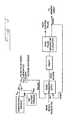
- FIG. 4is a circuit in a memory device of a preferred embodiment for temperature-based control of a write operation.
- this circuitcomprises a temperature sensor 410 and a reference voltage source 420 connected to a comparator 430 .
- the output of the comparator 430is connected to a pulse signal generator 440 .
- the temperature sensor 410 , reference voltage source 420 , comparator 430 , and pulse signal generator 440form a temperature-controlled pulse circuit.
- the pulse signal generator 440generates a pulse signal with voltage hysterisis and provides the pulse signal to an edge triggered flip-flop 450 , which takes the form of a latch in this preferred embodiment.
- a write block requested signalis provided to the set input of the edge triggered latch 450 , and a done signal from a write pulse generator and counter 480 is provided to the reset input of the edge triggered latch 450 .
- the output of the edge triggered latch 450is provided to a charge pump 460 , which is an on-chip programming voltage source that supplies a voltage level V pp for programming memory cells, and a delay 470 for the charge pump.
- the delay 470which can be implemented as a comparator that compares V pp to some desired reference voltage, is connected to the write pulse generator and counter 480 .
- the write pulse generator and counter 480comprises bitline/wordline selection circuitry and provides a write control pulse and a done signal to the memory array of the memory device.
- the done signal of the write pulse generator and counter 480is also provided to the reset input of the edge triggered latch 450 .
- the resetting of the latch 450disables the charge pump 460 , V pp falls, and the power dissipated in the leakage paths decreases.
- the resetting of the latch 450can trigger a discharge method for the memory array, as described in “Method and Apparatus for Discharging Memory Array Lines,” U.S. Patent application Ser. No. 09/897,784, filed Jun. 29, 2001 (MD-49). In either case, the voltages applied to the array decrease, and the power dissipated by the memory decreases.
- the temperature sensor 410either directly or indirectly senses the temperature of the memory array.
- the temperature sensor 410is located on the same silicon chip that comprises the memory array so that the sensed temperature is that of the memory array.
- the temperature sensor 410can be located on another component, such as interface circuitry, that is housed within the housing of the memory device.
- the temperature sensor 410provides a V out signal to the comparator 430 , and the comparator 430 compares V out to a reference voltage (V ref ) from the reference voltage source 420 . When V out reaches V ref , the comparator 430 generates an output signal.
- the threshold temperatureis 85° C.
- V refis 1.2 volts. To increase accuracy from about ⁇ 10° C.
- the reference voltage source 420be trimable.
- a test componentis heated to a desired threshold temperature, and non-volatile elements (e.g., a resistor tree) in the reference voltage source 420 are electrically adjusted until the comparator 430 provides an output signal.
- a trimable reference voltage source 420a trimable temperature sensor 410 can be used.
- the comparator 430When the temperature sensed by the temperature sensor 410 reaches the threshold temperature, the comparator 430 provides an output signal to the pulse signal generator 440 .
- the pulse signal generator 440generates a pulse signal (referred to herein as a “pause” pulse signal) that goes high when the monitored temperature reaches the threshold temperature and goes low when the monitored temperature is below the threshold temperature.
- the pulse signal generator 440Preferably, the pulse signal generator 440 generates the pause signal with voltage hysterisis so that there is a lag between a temperature drop and the effect of that drop.
- the pause signalinstead of causing the pause signal to go low in response to a small drop in temperature (e.g., a 1 micro-volt drop), the pause signal can go low in response to a larger drop in temperature (e.g., a 100 milli-volt drop). Accordingly, the use of voltage hysterisis prevents the temperature-controlled pulse circuit from generating a rapid series of pause signals.
- a small drop in temperaturee.g., a 1 micro-volt drop
- a larger drop in temperaturee.g., a 100 milli-volt drop
- the pause signalis provided to the edge triggered latch 450 , which latches a write block request signal upon the falling edge of the pause signal. If the temperature sensed by the temperature sensor 410 reaches the threshold temperature before a write block request goes high, the request is not latched, and the write-block signal is delayed. When the monitored temperature drops below the threshold temperature, the pause signal falls, and the falling edge of the pause signal latches the write block requested signal. The edge triggered latch 450 then provides a write block signal to enable the charge pump 460 .
- the write pulse generator and counter 480provides a series of write control pulses to the memory array to write a block of data (e.g., 512 bytes of data stored in a page register).
- a block of datae.g., 512 bytes of data stored in a page register.
- the edge triggered latch 450is reset only after the write pulse generator and counter 480 completes a block write. Accordingly, in this preferred embodiment, an in-progress write operation continues even if the temperature sensed by the temperature sensor 410 rises above the threshold temperature.
- the edge triggered latch 450will prevent a new write operation from being performed until the sensed temperature drops below the threshold temperature (i e., until the pause signal drops).
- the write-operation control circuitrycan be altered such that an in-progress write operation is interrupted when the sensed temperature reaches the threshold temperature.
- the previously-written datacan be re-written into the memory array.
- a determinationcan be made of what bits in the page register were stored in the memory array, and only those bits that were not stored are written when the write operation resumes. Such a determination can be made from the counter value in the write pulse generator and counter 480 or from a pointer used to indicate the last bit written to the memory array.
- the charge pumptakes the form disclosed in “Multi-Stage Charge Pump,” U.S. Patent application Ser. No. 09/809,878, and provides a programming pulse V pp of 9 to 10 volts.
- the write pulse generator and counter 480preferably uses the sensing-while-programming technique described in “Memory Device and Method for Sensing while Programming a Non-Volatile Memory Cell,” U.S. Patent application Ser. No. 09/896,815. Additional programming techniques are disclosed in “Method and Apparatus for Writing Memory Arrays Using External Source of High Programming Voltage,” U.S. Patent application Ser. No. 09/897,785 (Atty. Docket No.
- overheatingcan also occur during read operations.
- High read powercan occur when the sub-array size is very large and many sub-arrays are selected simultaneously for high data rate.
- the voltage across the leakage path reverse-biased diodescan be about 1.5 to 2.5 volts. Accordingly, the read mode leakage is less than the write mode leakage per sub-array.
- increasing the read mode data rate by selecting 64, 128, or more sub-arrayscan lead to read powers that can cause overheating.
- FIG. 5is an illustration of read operation control circuitry of a preferred embodiment. The operation of this circuitry is similar to that of the write operation control circuitry shown in FIG. 4 . Because the diode leakage current in read mode is less than the diode leakage current in write mode, thermal run-away occurs at a higher temperature in read mode than in write mode. Accordingly, the threshold temperature can be greater in read mode than in write mode.
- the V ref generated by the reference voltage source 520 in the read operation control circuitrycan be greater than the V ref generated by the reference voltage source 420 in the write operation control circuitry.
- the read operation control circuitry and write operation control circuitrycan share a temperature sensor or use different temperature sensors. Additionally, any of the alternatives discussed above with respect to the write operation control circuitry can be used with the read operation control circuitry.
- the memory arraycomprise a plurality of non-volatile passive element memory cells.
- the memory cellcomprises an antifuse and a diode. In its unprogrammed state, the antifuse is intact, and the memory cell holds a Logic 1. When suitable voltages are applied to the appropriate wordline and bitline, the antifuse of the memory cell is blown, and the diode is connected between the wordline and the bitline. This places the memory cell in a programmed (Logic 0) state.
- the un-programmed state of the memory cellcan be Logic 0, and the programmed state can be Logic 1.
- Memory cells that support multiple programmed statescan also be used. While write-many memory cells can be used, it is preferred that the memory cells be write-once memory cells. In a write-once memory cell, an original, un-programmed digital state of the memory cell (e.g., the Logic 1 state) cannot be restored once switched to a programmed digital state (e.g., the Logic 0 state).
- the memory cellscan be made from any suitable material.
- the memory cellsare preferably made from a semiconductor material; however, other materials such as phase-change materials and amorphous solids as well as those used with MRAM and organic passive element arrays can be used, as described in U.S. Pat. No. 6,055,180, which is hereby incorporated by reference.
- the memory arrayis preferably a three-dimensional memory array, which provides important economies in terms of reduced size and associated reductions in manufacturing cost. Suitable types of three-dimensional memory arrays are described in U.S. Pat. No. 6,034,882 to Johnson et al., U.S. Pat. No. 5,835,396 to Zhang, and U.S. patent application Ser. No. 09/560,626, all of which are hereby incorporated by reference. Additionally, in one preferred embodiment, the memory device takes the form of a compact, modular memory device that can be used with portable consumer products such as digital cameras, and the memory array of such a memory device is field-programmable, allowing the memory array to be programmed at a time after fabrication.
Landscapes
- Physics & Mathematics (AREA)
- General Physics & Mathematics (AREA)
- Read Only Memory (AREA)
Abstract
Description
Claims (72)
Priority Applications (1)
| Application Number | Priority Date | Filing Date | Title |
|---|---|---|---|
| US09/944,613US6735546B2 (en) | 2001-08-31 | 2001-08-31 | Memory device and method for temperature-based control over write and/or read operations |
Applications Claiming Priority (1)
| Application Number | Priority Date | Filing Date | Title |
|---|---|---|---|
| US09/944,613US6735546B2 (en) | 2001-08-31 | 2001-08-31 | Memory device and method for temperature-based control over write and/or read operations |
Publications (2)
| Publication Number | Publication Date |
|---|---|
| US20030046020A1 US20030046020A1 (en) | 2003-03-06 |
| US6735546B2true US6735546B2 (en) | 2004-05-11 |
Family
ID=25481722
Family Applications (1)
| Application Number | Title | Priority Date | Filing Date |
|---|---|---|---|
| US09/944,613Expired - LifetimeUS6735546B2 (en) | 2001-08-31 | 2001-08-31 | Memory device and method for temperature-based control over write and/or read operations |
Country Status (1)
| Country | Link |
|---|---|
| US (1) | US6735546B2 (en) |
Cited By (50)
| Publication number | Priority date | Publication date | Assignee | Title |
|---|---|---|---|---|
| US20030140265A1 (en)* | 2001-12-20 | 2003-07-24 | Michael Henninger | Method for controlling a safety-critical system which has a microcontroller |
| US20040179414A1 (en)* | 2003-03-10 | 2004-09-16 | Sharp Laboratories Of America, Inc. | Temperature compensated RRAM circuit |
| US20050174912A1 (en)* | 2003-11-26 | 2005-08-11 | Aritsune Nagamura | Apparatus and method for recording data in optical recording medium |
| US20060028886A1 (en)* | 2004-05-08 | 2006-02-09 | Byung-Gil Choi | Control of set/reset pulse in response to peripheral temperature in PRAM device |
| US20060109707A1 (en)* | 2004-11-23 | 2006-05-25 | Infineon Technologies North America Corp. | Energy adjusted write pulses in phase-change memories |
| US20060195289A1 (en)* | 2005-02-16 | 2006-08-31 | Samsung Electronics Co., Ltd. | Temperature sensor instruction signal generator and semiconductor memory device having the same |
| US20070058416A1 (en)* | 2004-06-08 | 2007-03-15 | Fujitsu Limited | Inspection method for semiconductor memory |
| US20070211512A1 (en)* | 2006-03-07 | 2007-09-13 | Susumu Shuto | Ferroelectric memory device |
| US7277343B1 (en) | 2006-05-24 | 2007-10-02 | Sandisk 3D Llc | Memory device with improved temperature-sensor circuit |
| US20070260616A1 (en)* | 2006-05-08 | 2007-11-08 | Eran Shen | Media with Pluggable Codec Methods |
| US20070260615A1 (en)* | 2006-05-08 | 2007-11-08 | Eran Shen | Media with Pluggable Codec |
| US20080106928A1 (en)* | 2006-09-20 | 2008-05-08 | Thomas Happ | Energy adjusted write pulses in phase-change memory cells |
| US20080120485A1 (en)* | 2006-11-20 | 2008-05-22 | Rothman Michael A | Methods and apparatus to manage throttling in computing environments |
| US20090113116A1 (en)* | 2007-10-30 | 2009-04-30 | Thompson E Earle | Digital content kiosk and methods for use therewith |
| US20090323400A1 (en)* | 2008-06-27 | 2009-12-31 | Renesas Technology Corp. | Semiconductor device |
| US20100073069A1 (en)* | 2008-09-22 | 2010-03-25 | Yuxin Wang | On-Chip Bias Voltage Temperature Coefficient Self-Calibration Mechanism |
| US20100095847A1 (en)* | 2008-10-16 | 2010-04-22 | William Steven Lopes | System for conditioning fluids utilizing a magnetic fluid processor |
| US20110047437A1 (en)* | 2006-12-06 | 2011-02-24 | Fusion-Io, Inc. | Apparatus, system, and method for graceful cache device degradation |
| US20110060927A1 (en)* | 2009-09-09 | 2011-03-10 | Fusion-Io, Inc. | Apparatus, system, and method for power reduction in a storage device |
| US8004917B2 (en) | 2008-09-22 | 2011-08-23 | Sandisk Technologies Inc. | Bandgap voltage and temperature coefficient trimming algorithm |
| US20120106242A1 (en)* | 2010-10-29 | 2012-05-03 | Hynix Semiconductor Inc. | Memory apparatus having storage medium dependent on temperature and method for driving the same |
| US8489817B2 (en) | 2007-12-06 | 2013-07-16 | Fusion-Io, Inc. | Apparatus, system, and method for caching data |
| US8527693B2 (en) | 2010-12-13 | 2013-09-03 | Fusion IO, Inc. | Apparatus, system, and method for auto-commit memory |
| US8542000B1 (en) | 2012-03-19 | 2013-09-24 | Sandisk Technologies Inc. | Curvature compensated band-gap design |
| US20140005854A1 (en)* | 2010-07-15 | 2014-01-02 | Seagate Technology Llc | Temperature monitoring systems and methods |
| US8694719B2 (en) | 2011-06-24 | 2014-04-08 | Sandisk Technologies Inc. | Controller, storage device, and method for power throttling memory operations |
| US8706968B2 (en) | 2007-12-06 | 2014-04-22 | Fusion-Io, Inc. | Apparatus, system, and method for redundant write caching |
| US8825937B2 (en) | 2011-02-25 | 2014-09-02 | Fusion-Io, Inc. | Writing cached data forward on read |
| US8941369B2 (en) | 2012-03-19 | 2015-01-27 | Sandisk Technologies Inc. | Curvature compensated band-gap design trimmable at a single temperature |
| US8966184B2 (en) | 2011-01-31 | 2015-02-24 | Intelligent Intellectual Property Holdings 2, LLC. | Apparatus, system, and method for managing eviction of data |
| US8972627B2 (en) | 2009-09-09 | 2015-03-03 | Fusion-Io, Inc. | Apparatus, system, and method for managing operations for data storage media |
| US8984216B2 (en) | 2010-09-09 | 2015-03-17 | Fusion-Io, Llc | Apparatus, system, and method for managing lifetime of a storage device |
| US9021158B2 (en) | 2009-09-09 | 2015-04-28 | SanDisk Technologies, Inc. | Program suspend/resume for memory |
| US9047178B2 (en) | 2010-12-13 | 2015-06-02 | SanDisk Technologies, Inc. | Auto-commit memory synchronization |
| US9104599B2 (en) | 2007-12-06 | 2015-08-11 | Intelligent Intellectual Property Holdings 2 Llc | Apparatus, system, and method for destaging cached data |
| US9208071B2 (en) | 2010-12-13 | 2015-12-08 | SanDisk Technologies, Inc. | Apparatus, system, and method for accessing memory |
| US9218278B2 (en) | 2010-12-13 | 2015-12-22 | SanDisk Technologies, Inc. | Auto-commit memory |
| US9223514B2 (en) | 2009-09-09 | 2015-12-29 | SanDisk Technologies, Inc. | Erase suspend/resume for memory |
| US9251086B2 (en) | 2012-01-24 | 2016-02-02 | SanDisk Technologies, Inc. | Apparatus, system, and method for managing a cache |
| US9519540B2 (en) | 2007-12-06 | 2016-12-13 | Sandisk Technologies Llc | Apparatus, system, and method for destaging cached data |
| US9541456B2 (en) | 2014-02-07 | 2017-01-10 | Sandisk Technologies Llc | Reference voltage generator for temperature sensor with trimming capability at two temperatures |
| US9600184B2 (en) | 2007-12-06 | 2017-03-21 | Sandisk Technologies Llc | Apparatus, system, and method for coordinating storage requests in a multi-processor/multi-thread environment |
| US9666244B2 (en) | 2014-03-01 | 2017-05-30 | Fusion-Io, Inc. | Dividing a storage procedure |
| US9715913B1 (en) | 2015-07-30 | 2017-07-25 | Sandisk Technologies Llc | Temperature code circuit with single ramp for calibration and determination |
| US9734086B2 (en) | 2006-12-06 | 2017-08-15 | Sandisk Technologies Llc | Apparatus, system, and method for a device shared between multiple independent hosts |
| US9767032B2 (en) | 2012-01-12 | 2017-09-19 | Sandisk Technologies Llc | Systems and methods for cache endurance |
| US9798469B2 (en) | 2014-07-31 | 2017-10-24 | Samsung Electronics Co., Ltd. | Storage device and controlling method thereof |
| US9922699B1 (en)* | 2016-11-30 | 2018-03-20 | Apple Inc. | Adaptive diode sizing techniques for reducing memory power leakage |
| US10817421B2 (en) | 2010-12-13 | 2020-10-27 | Sandisk Technologies Llc | Persistent data structures |
| US10817502B2 (en) | 2010-12-13 | 2020-10-27 | Sandisk Technologies Llc | Persistent memory management |
Families Citing this family (13)
| Publication number | Priority date | Publication date | Assignee | Title |
|---|---|---|---|---|
| US6954394B2 (en)* | 2002-11-27 | 2005-10-11 | Matrix Semiconductor, Inc. | Integrated circuit and method for selecting a set of memory-cell-layer-dependent or temperature-dependent operating conditions |
| US7057958B2 (en)* | 2003-09-30 | 2006-06-06 | Sandisk Corporation | Method and system for temperature compensation for memory cells with temperature-dependent behavior |
| US7218570B2 (en)* | 2004-12-17 | 2007-05-15 | Sandisk 3D Llc | Apparatus and method for memory operations using address-dependent conditions |
| US9142322B2 (en)* | 2012-08-10 | 2015-09-22 | Stmicroelectronics International N.V. | Memory manager |
| US9406368B2 (en)* | 2014-01-21 | 2016-08-02 | International Business Machines Corporation | Dynamic temperature adjustments in spin transfer torque magnetoresistive random-access memory (STT-MRAM) |
| US9418721B2 (en) | 2014-01-21 | 2016-08-16 | International Business Machines Corporation | Determining and storing bit error rate relationships in spin transfer torque magnetoresistive random-access memory (STT-MRAM) |
| FR3025927B1 (en)* | 2014-09-12 | 2018-01-12 | St Microelectronics Sa | PROGRAMMING ANTI-FUSIBLE CELLS |
| US9978432B2 (en) | 2014-12-22 | 2018-05-22 | Intel Corporation | Write operations in spin transfer torque memory |
| US10990299B2 (en)* | 2018-03-26 | 2021-04-27 | Lenovo Enterprise Solutions (Singapore) Pte. Ltd | Storing data based on the physical accessibility of data storage devices |
| US11429504B2 (en) | 2020-08-13 | 2022-08-30 | Micron Technology, Inc. | Closing block family based on soft and hard closure criteria |
| US11940892B2 (en)* | 2019-12-19 | 2024-03-26 | Micron Technology, Inc. | Closing block family based on soft and hard closure criteria |
| CN113448489B (en)* | 2020-03-25 | 2024-06-18 | 慧荣科技股份有限公司 | Computer readable storage medium, method and apparatus for controlling access to flash memory card |
| KR20230021455A (en)* | 2021-08-05 | 2023-02-14 | 에스케이하이닉스 주식회사 | Memory device and operating method thereof |
Citations (30)
| Publication number | Priority date | Publication date | Assignee | Title |
|---|---|---|---|---|
| US3851316A (en) | 1971-09-07 | 1974-11-26 | Tokyo Shibaura Electric Co | Semiconductor memory device |
| US4592027A (en)* | 1983-02-15 | 1986-05-27 | Sharp Kabushiki Kaisha | Read control circuit in a read only memory system |
| US4646266A (en) | 1984-09-28 | 1987-02-24 | Energy Conversion Devices, Inc. | Programmable semiconductor structures and methods for using the same |
| US4646269A (en) | 1984-09-18 | 1987-02-24 | Monolithic Memories, Inc. | Multiple programmable initialize words in a programmable read only memory |
| US4698788A (en) | 1985-07-01 | 1987-10-06 | Motorola, Inc. | Memory architecture with sub-arrays |
| US4744061A (en) | 1983-11-25 | 1988-05-10 | Fujitsu Limited | Dynamic semiconductor memory device having a simultaneous test function for divided memory cell blocks |
| US4873669A (en) | 1986-07-30 | 1989-10-10 | Mitsubishi Denki Kabushiki Kaisha | Random access memory device operable in a normal mode and in a test mode |
| US5107139A (en)* | 1990-03-30 | 1992-04-21 | Texas Instruments Incorporated | On-chip transient event detector |
| US5149199A (en)* | 1990-05-24 | 1992-09-22 | Kabushiki Kaisha Toshiba | Temperature detection circuit used in thermal shielding circuit |
| US5276649A (en) | 1989-03-16 | 1994-01-04 | Mitsubishi Denki Kabushiki Kaisha | Dynamic-type semiconductor memory device having staggered activation of column groups |
| US5278796A (en) | 1991-04-12 | 1994-01-11 | Micron Technology, Inc. | Temperature-dependent DRAM refresh circuit |
| US5359571A (en) | 1993-01-27 | 1994-10-25 | Yu Shih Chiang | Memory array having a plurality of address partitions |
| US5383157A (en) | 1993-08-06 | 1995-01-17 | Cypress Semiconductor Corporation | Parallel TESTMODE |
| US5410512A (en) | 1992-05-22 | 1995-04-25 | Kabushiki Kaisha Toshiba | Semiconductor memory device |
| US5784328A (en)* | 1996-12-23 | 1998-07-21 | Lsi Logic Corporation | Memory system including an on-chip temperature sensor for regulating the refresh rate of a DRAM array |
| US5835396A (en) | 1996-10-17 | 1998-11-10 | Zhang; Guobiao | Three-dimensional read-only memory |
| US5890100A (en)* | 1997-08-19 | 1999-03-30 | Advanced Micro Devices, Inc. | Chip temperature monitor using delay lines |
| US5925996A (en) | 1997-10-10 | 1999-07-20 | Whistler Corporation Of Massachusetts | Garage door operator motor secondary thermal overload |
| US5940340A (en)* | 1993-06-14 | 1999-08-17 | Rambus, Inc. | Method and apparatus for writing to memory components |
| US5961215A (en) | 1997-09-26 | 1999-10-05 | Advanced Micro Devices, Inc. | Temperature sensor integral with microprocessor and methods of using same |
| US5977746A (en)* | 1998-07-21 | 1999-11-02 | Stryker Corporation | Rechargeable battery pack and method for manufacturing same |
| US6034882A (en) | 1998-11-16 | 2000-03-07 | Matrix Semiconductor, Inc. | Vertically stacked field programmable nonvolatile memory and method of fabrication |
| US6034918A (en) | 1990-04-18 | 2000-03-07 | Rambus Inc. | Method of operating a memory having a variable data output length and a programmable register |
| US6055180A (en) | 1997-06-17 | 2000-04-25 | Thin Film Electronics Asa | Electrically addressable passive device, method for electrical addressing of the same and uses of the device and the method |
| US6185712B1 (en) | 1998-07-02 | 2001-02-06 | International Business Machines Corporation | Chip performance optimization with self programmed built in self test |
| US6212121B1 (en) | 1998-12-02 | 2001-04-03 | Samsung Electronics Co., Ltd. | Semiconductor memory device with multiple sub-arrays of different sizes |
| US6236587B1 (en) | 1997-09-01 | 2001-05-22 | Thin Film Electronics Asa | Read-only memory and read-only memory devices |
| US6373768B2 (en)* | 1998-07-16 | 2002-04-16 | Rambus Inc | Apparatus and method for thermal regulation in memory subsystems |
| US6385074B1 (en)* | 1998-11-16 | 2002-05-07 | Matrix Semiconductor, Inc. | Integrated circuit structure including three-dimensional memory array |
| US6560152B1 (en) | 2001-11-02 | 2003-05-06 | Sandisk Corporation | Non-volatile memory with temperature-compensated data read |
- 2001
- 2001-08-31USUS09/944,613patent/US6735546B2/ennot_activeExpired - Lifetime
Patent Citations (31)
| Publication number | Priority date | Publication date | Assignee | Title |
|---|---|---|---|---|
| US3851316A (en) | 1971-09-07 | 1974-11-26 | Tokyo Shibaura Electric Co | Semiconductor memory device |
| US4592027A (en)* | 1983-02-15 | 1986-05-27 | Sharp Kabushiki Kaisha | Read control circuit in a read only memory system |
| US4744061A (en) | 1983-11-25 | 1988-05-10 | Fujitsu Limited | Dynamic semiconductor memory device having a simultaneous test function for divided memory cell blocks |
| US4646269A (en) | 1984-09-18 | 1987-02-24 | Monolithic Memories, Inc. | Multiple programmable initialize words in a programmable read only memory |
| US4646266A (en) | 1984-09-28 | 1987-02-24 | Energy Conversion Devices, Inc. | Programmable semiconductor structures and methods for using the same |
| US4698788A (en) | 1985-07-01 | 1987-10-06 | Motorola, Inc. | Memory architecture with sub-arrays |
| US4873669A (en) | 1986-07-30 | 1989-10-10 | Mitsubishi Denki Kabushiki Kaisha | Random access memory device operable in a normal mode and in a test mode |
| US5276649A (en) | 1989-03-16 | 1994-01-04 | Mitsubishi Denki Kabushiki Kaisha | Dynamic-type semiconductor memory device having staggered activation of column groups |
| US5107139A (en)* | 1990-03-30 | 1992-04-21 | Texas Instruments Incorporated | On-chip transient event detector |
| US6034918A (en) | 1990-04-18 | 2000-03-07 | Rambus Inc. | Method of operating a memory having a variable data output length and a programmable register |
| US6070222A (en) | 1990-04-18 | 2000-05-30 | Rambus Inc. | Synchronous memory device having identification register |
| US5149199A (en)* | 1990-05-24 | 1992-09-22 | Kabushiki Kaisha Toshiba | Temperature detection circuit used in thermal shielding circuit |
| US5278796A (en) | 1991-04-12 | 1994-01-11 | Micron Technology, Inc. | Temperature-dependent DRAM refresh circuit |
| US5410512A (en) | 1992-05-22 | 1995-04-25 | Kabushiki Kaisha Toshiba | Semiconductor memory device |
| US5359571A (en) | 1993-01-27 | 1994-10-25 | Yu Shih Chiang | Memory array having a plurality of address partitions |
| US5940340A (en)* | 1993-06-14 | 1999-08-17 | Rambus, Inc. | Method and apparatus for writing to memory components |
| US5383157A (en) | 1993-08-06 | 1995-01-17 | Cypress Semiconductor Corporation | Parallel TESTMODE |
| US5835396A (en) | 1996-10-17 | 1998-11-10 | Zhang; Guobiao | Three-dimensional read-only memory |
| US5784328A (en)* | 1996-12-23 | 1998-07-21 | Lsi Logic Corporation | Memory system including an on-chip temperature sensor for regulating the refresh rate of a DRAM array |
| US6055180A (en) | 1997-06-17 | 2000-04-25 | Thin Film Electronics Asa | Electrically addressable passive device, method for electrical addressing of the same and uses of the device and the method |
| US5890100A (en)* | 1997-08-19 | 1999-03-30 | Advanced Micro Devices, Inc. | Chip temperature monitor using delay lines |
| US6236587B1 (en) | 1997-09-01 | 2001-05-22 | Thin Film Electronics Asa | Read-only memory and read-only memory devices |
| US5961215A (en) | 1997-09-26 | 1999-10-05 | Advanced Micro Devices, Inc. | Temperature sensor integral with microprocessor and methods of using same |
| US5925996A (en) | 1997-10-10 | 1999-07-20 | Whistler Corporation Of Massachusetts | Garage door operator motor secondary thermal overload |
| US6185712B1 (en) | 1998-07-02 | 2001-02-06 | International Business Machines Corporation | Chip performance optimization with self programmed built in self test |
| US6373768B2 (en)* | 1998-07-16 | 2002-04-16 | Rambus Inc | Apparatus and method for thermal regulation in memory subsystems |
| US5977746A (en)* | 1998-07-21 | 1999-11-02 | Stryker Corporation | Rechargeable battery pack and method for manufacturing same |
| US6034882A (en) | 1998-11-16 | 2000-03-07 | Matrix Semiconductor, Inc. | Vertically stacked field programmable nonvolatile memory and method of fabrication |
| US6385074B1 (en)* | 1998-11-16 | 2002-05-07 | Matrix Semiconductor, Inc. | Integrated circuit structure including three-dimensional memory array |
| US6212121B1 (en) | 1998-12-02 | 2001-04-03 | Samsung Electronics Co., Ltd. | Semiconductor memory device with multiple sub-arrays of different sizes |
| US6560152B1 (en) | 2001-11-02 | 2003-05-06 | Sandisk Corporation | Non-volatile memory with temperature-compensated data read |
Non-Patent Citations (3)
| Title |
|---|
| "A 14ns 1MB CMOS SRAM with Variable Bit-Organization," Wada et al., 1988 IEEE International Solid-State Circuits Conference, pp. 252-253 ( Feb. 19, 1988). |
| "Partial Selection of Passive Element Memory Cell Sub-Arrays for Write Operation," U.S. patent application Ser. No. 09/748,649, filed Dec. 22, 2000; inventors: Roy E. Scheuerlein and Matthew P. Crowley. |
| Information Disclosure Statement, 2 pages (Nov. 15, 2001). |
Cited By (94)
| Publication number | Priority date | Publication date | Assignee | Title |
|---|---|---|---|---|
| US7171582B2 (en)* | 2001-12-20 | 2007-01-30 | Siemens Aktiengesellschaft | Method for controlling a safety-critical system which has a microcontroller |
| US20030140265A1 (en)* | 2001-12-20 | 2003-07-24 | Michael Henninger | Method for controlling a safety-critical system which has a microcontroller |
| US20040179414A1 (en)* | 2003-03-10 | 2004-09-16 | Sharp Laboratories Of America, Inc. | Temperature compensated RRAM circuit |
| US6868025B2 (en)* | 2003-03-10 | 2005-03-15 | Sharp Laboratories Of America, Inc. | Temperature compensated RRAM circuit |
| US20050127403A1 (en)* | 2003-03-10 | 2005-06-16 | Sharp Laboratories Of America, Inc. | RRAM circuit with temperature compensation |
| US6967884B2 (en)* | 2003-03-10 | 2005-11-22 | Sharp Laboratories Of America, Inc. | RRAM circuit with temperature compensation |
| US20050174912A1 (en)* | 2003-11-26 | 2005-08-11 | Aritsune Nagamura | Apparatus and method for recording data in optical recording medium |
| US7457225B2 (en)* | 2003-11-26 | 2008-11-25 | Ricoh Company, Ltd. | Apparatus and method for recording data in optical recording medium |
| US7796425B2 (en)* | 2004-05-08 | 2010-09-14 | Samsung Electronics Co., Ltd. | Control of set/reset pulse in response to peripheral temperature in PRAM device |
| US7315469B2 (en)* | 2004-05-08 | 2008-01-01 | Samsung Electronics Co., Ltd. | Control of set/reset pulse in response to peripheral temperature in PRAM device |
| US20060028886A1 (en)* | 2004-05-08 | 2006-02-09 | Byung-Gil Choi | Control of set/reset pulse in response to peripheral temperature in PRAM device |
| US20080212362A1 (en)* | 2004-05-08 | 2008-09-04 | Byung-Gil Choi | Control of set/reset pulse in response to peripheral temperature in pram device |
| US20070058416A1 (en)* | 2004-06-08 | 2007-03-15 | Fujitsu Limited | Inspection method for semiconductor memory |
| US7982466B2 (en)* | 2004-06-08 | 2011-07-19 | Fujitsu Semiconductor Limited | Inspection method for semiconductor memory |
| US7113424B2 (en)* | 2004-11-23 | 2006-09-26 | Infineon Technologies Ag | Energy adjusted write pulses in phase-change memories |
| US20070014173A1 (en)* | 2004-11-23 | 2007-01-18 | Infineon Technologies Ag. | Energy adjusted write pulses in phase-change memories |
| US20060109707A1 (en)* | 2004-11-23 | 2006-05-25 | Infineon Technologies North America Corp. | Energy adjusted write pulses in phase-change memories |
| US7327623B2 (en) | 2004-11-23 | 2008-02-05 | Infineon Technologies Ag | Energy adjusted write pulses in phase-change memories |
| US20060195289A1 (en)* | 2005-02-16 | 2006-08-31 | Samsung Electronics Co., Ltd. | Temperature sensor instruction signal generator and semiconductor memory device having the same |
| US7499359B2 (en) | 2005-02-16 | 2009-03-03 | Samsung Electronics Co., Ltd. | Temperature sensor instruction signal generator and semiconductor memory device having the same |
| US20070211512A1 (en)* | 2006-03-07 | 2007-09-13 | Susumu Shuto | Ferroelectric memory device |
| US7663905B2 (en)* | 2006-03-07 | 2010-02-16 | Kabushiki Kaisha Toshiba | Ferroelectric memory device and data read method in same |
| US20070267474A1 (en)* | 2006-05-08 | 2007-11-22 | Eran Shen | Secure storage digital kiosk distribution methods |
| US20070260615A1 (en)* | 2006-05-08 | 2007-11-08 | Eran Shen | Media with Pluggable Codec |
| US20070282747A1 (en)* | 2006-05-08 | 2007-12-06 | Eran Shen | Secure storage digital kiosk distribution |
| US20070260616A1 (en)* | 2006-05-08 | 2007-11-08 | Eran Shen | Media with Pluggable Codec Methods |
| US9680686B2 (en) | 2006-05-08 | 2017-06-13 | Sandisk Technologies Llc | Media with pluggable codec methods |
| US7277343B1 (en) | 2006-05-24 | 2007-10-02 | Sandisk 3D Llc | Memory device with improved temperature-sensor circuit |
| US7283414B1 (en) | 2006-05-24 | 2007-10-16 | Sandisk 3D Llc | Method for improving the precision of a temperature-sensor circuit |
| US20080106928A1 (en)* | 2006-09-20 | 2008-05-08 | Thomas Happ | Energy adjusted write pulses in phase-change memory cells |
| US7859894B2 (en)* | 2006-09-20 | 2010-12-28 | Qimonda Ag | Energy adjusted write pulses in phase-change memory cells |
| US7596714B2 (en)* | 2006-11-20 | 2009-09-29 | Intel Corporation | Methods and apparatus to manage throttling in computing environments |
| US20080120485A1 (en)* | 2006-11-20 | 2008-05-22 | Rothman Michael A | Methods and apparatus to manage throttling in computing environments |
| US11573909B2 (en) | 2006-12-06 | 2023-02-07 | Unification Technologies Llc | Apparatus, system, and method for managing commands of solid-state storage using bank interleave |
| US11640359B2 (en) | 2006-12-06 | 2023-05-02 | Unification Technologies Llc | Systems and methods for identifying storage resources that are not in use |
| US8756375B2 (en) | 2006-12-06 | 2014-06-17 | Fusion-Io, Inc. | Non-volatile cache |
| US20110047437A1 (en)* | 2006-12-06 | 2011-02-24 | Fusion-Io, Inc. | Apparatus, system, and method for graceful cache device degradation |
| US11960412B2 (en) | 2006-12-06 | 2024-04-16 | Unification Technologies Llc | Systems and methods for identifying storage resources that are not in use |
| US11847066B2 (en) | 2006-12-06 | 2023-12-19 | Unification Technologies Llc | Apparatus, system, and method for managing commands of solid-state storage using bank interleave |
| US8443134B2 (en) | 2006-12-06 | 2013-05-14 | Fusion-Io, Inc. | Apparatus, system, and method for graceful cache device degradation |
| US9734086B2 (en) | 2006-12-06 | 2017-08-15 | Sandisk Technologies Llc | Apparatus, system, and method for a device shared between multiple independent hosts |
| US20090113116A1 (en)* | 2007-10-30 | 2009-04-30 | Thompson E Earle | Digital content kiosk and methods for use therewith |
| US9519540B2 (en) | 2007-12-06 | 2016-12-13 | Sandisk Technologies Llc | Apparatus, system, and method for destaging cached data |
| US9600184B2 (en) | 2007-12-06 | 2017-03-21 | Sandisk Technologies Llc | Apparatus, system, and method for coordinating storage requests in a multi-processor/multi-thread environment |
| US8706968B2 (en) | 2007-12-06 | 2014-04-22 | Fusion-Io, Inc. | Apparatus, system, and method for redundant write caching |
| US8489817B2 (en) | 2007-12-06 | 2013-07-16 | Fusion-Io, Inc. | Apparatus, system, and method for caching data |
| US9104599B2 (en) | 2007-12-06 | 2015-08-11 | Intelligent Intellectual Property Holdings 2 Llc | Apparatus, system, and method for destaging cached data |
| US7961500B2 (en)* | 2008-06-27 | 2011-06-14 | Renesas Electronics Corporation | Semiconductor device |
| US20090323400A1 (en)* | 2008-06-27 | 2009-12-31 | Renesas Technology Corp. | Semiconductor device |
| US8279696B2 (en) | 2008-06-27 | 2012-10-02 | Renesas Electronics Corporation | Semiconductor device |
| US8611166B2 (en) | 2008-06-27 | 2013-12-17 | Renesas Electronics Corporation | Semiconductor device |
| US8228739B2 (en) | 2008-09-22 | 2012-07-24 | Sandisk Technologies Inc. | Bandgap voltage and temperature coefficient trimming algorithm |
| US8004917B2 (en) | 2008-09-22 | 2011-08-23 | Sandisk Technologies Inc. | Bandgap voltage and temperature coefficient trimming algorithm |
| US20100073069A1 (en)* | 2008-09-22 | 2010-03-25 | Yuxin Wang | On-Chip Bias Voltage Temperature Coefficient Self-Calibration Mechanism |
| US7889575B2 (en) | 2008-09-22 | 2011-02-15 | Sandisk Corporation | On-chip bias voltage temperature coefficient self-calibration mechanism |
| US20100095847A1 (en)* | 2008-10-16 | 2010-04-22 | William Steven Lopes | System for conditioning fluids utilizing a magnetic fluid processor |
| US8289801B2 (en) | 2009-09-09 | 2012-10-16 | Fusion-Io, Inc. | Apparatus, system, and method for power reduction management in a storage device |
| US9223514B2 (en) | 2009-09-09 | 2015-12-29 | SanDisk Technologies, Inc. | Erase suspend/resume for memory |
| US20110060927A1 (en)* | 2009-09-09 | 2011-03-10 | Fusion-Io, Inc. | Apparatus, system, and method for power reduction in a storage device |
| US8429436B2 (en) | 2009-09-09 | 2013-04-23 | Fusion-Io, Inc. | Apparatus, system, and method for power reduction in a storage device |
| US8972627B2 (en) | 2009-09-09 | 2015-03-03 | Fusion-Io, Inc. | Apparatus, system, and method for managing operations for data storage media |
| US9021158B2 (en) | 2009-09-09 | 2015-04-28 | SanDisk Technologies, Inc. | Program suspend/resume for memory |
| WO2011031899A3 (en)* | 2009-09-09 | 2011-06-16 | Fusion-Io, Inc. | Apparatus, system, and method for power reduction in a storage device |
| US9305610B2 (en) | 2009-09-09 | 2016-04-05 | SanDisk Technologies, Inc. | Apparatus, system, and method for power reduction management in a storage device |
| US20110058440A1 (en)* | 2009-09-09 | 2011-03-10 | Fusion-Io, Inc. | Apparatus, system, and method for power reduction management in a storage device |
| US9753442B2 (en)* | 2010-07-15 | 2017-09-05 | Seagate Technology Llc | Temperature monitoring systems and methods |
| US20140005854A1 (en)* | 2010-07-15 | 2014-01-02 | Seagate Technology Llc | Temperature monitoring systems and methods |
| US8984216B2 (en) | 2010-09-09 | 2015-03-17 | Fusion-Io, Llc | Apparatus, system, and method for managing lifetime of a storage device |
| US20120106242A1 (en)* | 2010-10-29 | 2012-05-03 | Hynix Semiconductor Inc. | Memory apparatus having storage medium dependent on temperature and method for driving the same |
| US8331183B2 (en)* | 2010-10-29 | 2012-12-11 | SK Hynix Inc. | Memory apparatus having storage medium dependent on temperature and method for driving the same |
| US9223662B2 (en) | 2010-12-13 | 2015-12-29 | SanDisk Technologies, Inc. | Preserving data of a volatile memory |
| US9208071B2 (en) | 2010-12-13 | 2015-12-08 | SanDisk Technologies, Inc. | Apparatus, system, and method for accessing memory |
| US9218278B2 (en) | 2010-12-13 | 2015-12-22 | SanDisk Technologies, Inc. | Auto-commit memory |
| US9047178B2 (en) | 2010-12-13 | 2015-06-02 | SanDisk Technologies, Inc. | Auto-commit memory synchronization |
| US9767017B2 (en) | 2010-12-13 | 2017-09-19 | Sandisk Technologies Llc | Memory device with volatile and non-volatile media |
| US8527693B2 (en) | 2010-12-13 | 2013-09-03 | Fusion IO, Inc. | Apparatus, system, and method for auto-commit memory |
| US10817502B2 (en) | 2010-12-13 | 2020-10-27 | Sandisk Technologies Llc | Persistent memory management |
| US10817421B2 (en) | 2010-12-13 | 2020-10-27 | Sandisk Technologies Llc | Persistent data structures |
| US9772938B2 (en) | 2010-12-13 | 2017-09-26 | Sandisk Technologies Llc | Auto-commit memory metadata and resetting the metadata by writing to special address in free space of page storing the metadata |
| US9092337B2 (en) | 2011-01-31 | 2015-07-28 | Intelligent Intellectual Property Holdings 2 Llc | Apparatus, system, and method for managing eviction of data |
| US8966184B2 (en) | 2011-01-31 | 2015-02-24 | Intelligent Intellectual Property Holdings 2, LLC. | Apparatus, system, and method for managing eviction of data |
| US9141527B2 (en) | 2011-02-25 | 2015-09-22 | Intelligent Intellectual Property Holdings 2 Llc | Managing cache pools |
| US8825937B2 (en) | 2011-02-25 | 2014-09-02 | Fusion-Io, Inc. | Writing cached data forward on read |
| US8694719B2 (en) | 2011-06-24 | 2014-04-08 | Sandisk Technologies Inc. | Controller, storage device, and method for power throttling memory operations |
| US9767032B2 (en) | 2012-01-12 | 2017-09-19 | Sandisk Technologies Llc | Systems and methods for cache endurance |
| US9251086B2 (en) | 2012-01-24 | 2016-02-02 | SanDisk Technologies, Inc. | Apparatus, system, and method for managing a cache |
| US8542000B1 (en) | 2012-03-19 | 2013-09-24 | Sandisk Technologies Inc. | Curvature compensated band-gap design |
| US8941369B2 (en) | 2012-03-19 | 2015-01-27 | Sandisk Technologies Inc. | Curvature compensated band-gap design trimmable at a single temperature |
| US9683904B2 (en) | 2014-02-07 | 2017-06-20 | Sandisk Technologies Llc | Reference voltage generator for temperature sensor with trimming capability at two temperatures |
| US9541456B2 (en) | 2014-02-07 | 2017-01-10 | Sandisk Technologies Llc | Reference voltage generator for temperature sensor with trimming capability at two temperatures |
| US9666244B2 (en) | 2014-03-01 | 2017-05-30 | Fusion-Io, Inc. | Dividing a storage procedure |
| US9798469B2 (en) | 2014-07-31 | 2017-10-24 | Samsung Electronics Co., Ltd. | Storage device and controlling method thereof |
| US9715913B1 (en) | 2015-07-30 | 2017-07-25 | Sandisk Technologies Llc | Temperature code circuit with single ramp for calibration and determination |
| US9922699B1 (en)* | 2016-11-30 | 2018-03-20 | Apple Inc. | Adaptive diode sizing techniques for reducing memory power leakage |
Also Published As
| Publication number | Publication date |
|---|---|
| US20030046020A1 (en) | 2003-03-06 |
Similar Documents
| Publication | Publication Date | Title |
|---|---|---|
| US6735546B2 (en) | Memory device and method for temperature-based control over write and/or read operations | |
| JP4567963B2 (en) | Semiconductor integrated circuit device | |
| US7190607B2 (en) | Phase-change memory element driver circuits using measurement to control current and methods of controlling drive current of phase-change memory elements using measurement | |
| US7391638B2 (en) | Memory device for protecting memory cells during programming | |
| US7405964B2 (en) | Integrated circuit to identify read disturb condition in memory cell | |
| US7580278B2 (en) | Variable resistance memory device | |
| US7457152B2 (en) | Non-volatile memory devices and systems including phase-change one-time-programmable (OTP) memory cells and related methods | |
| US7577024B2 (en) | Streaming mode programming in phase change memories | |
| US8531904B2 (en) | Methods and apparatus for extending the effective thermal operating range of a memory | |
| US20090010051A1 (en) | Reading a phase change memory | |
| KR20110102734A (en) | Nonvolatile Semiconductor Memory Device with OTP Lock Bit Register | |
| KR102047947B1 (en) | Integrated circuit chip, memory device and e-fuse array circuit | |
| JP2006079812A (en) | Semiconductor memory device and read operation method | |
| WO2006088635A1 (en) | Resetting phase change memory bits | |
| US20090201721A1 (en) | Phase change memory device and write method thereof | |
| US6724665B2 (en) | Memory device and method for selectable sub-array activation | |
| US7760545B2 (en) | Semiconductor memory device and programming method thereof | |
| US7589989B2 (en) | Method for protecting memory cells during programming | |
| JP4786948B2 (en) | PROGRAMMING METHOD, PHASE CHANGE MEMORY DEVICE, AND DRIVE CIRCUIT FOR PHASE CHANGE MEMORY WRITE OPERATION | |
| US7352616B2 (en) | Phase change random access memory, boosting charge pump and method of generating write driving voltage | |
| KR102452623B1 (en) | Operation method and resistive memory device for reducing write latency | |
| KR101416878B1 (en) | Power supply circuit and phase change memory device having the same | |
| Ramaswamy et al. | Progress on design and demonstration of the 4Mb chalcogenide-based random access memory | |
| WO2008051835A1 (en) | Memory device and method for protecting memory cells during programming | |
| WO2009070635A1 (en) | Analog access circuit for validating chalcogenide memory cells |
Legal Events
| Date | Code | Title | Description |
|---|---|---|---|
| AS | Assignment | Owner name:MATRIX SEMICONDUCTOR, INC., CALIFORNIA Free format text:ASSIGNMENT OF ASSIGNORS INTEREST;ASSIGNOR:SCHEUERLEIN, ROY E.;REEL/FRAME:012138/0001 Effective date:20010830 | |
| AS | Assignment | Owner name:VENTURE LENDING & LEASING III, INC., AS AGENT, CAL Free format text:SECURITY AGREEMENT;ASSIGNOR:MATRIX SEMICONDUCTOR, INC.;REEL/FRAME:012831/0698 Effective date:20020405 | |
| AS | Assignment | Owner name:SILICON VALLEY BANK, CALIFORNIA Free format text:SECURITY AGREEMENT;ASSIGNOR:MATRIX SEMICONDUCTOR, INC.;REEL/FRAME:012994/0547 Effective date:20020425 | |
| STCF | Information on status: patent grant | Free format text:PATENTED CASE | |
| AS | Assignment | Owner name:SANDISK 3D LLC,CALIFORNIA Free format text:MERGER;ASSIGNOR:MATRIX SEMICONDUCTOR, INC.;REEL/FRAME:017544/0769 Effective date:20051020 Owner name:SANDISK 3D LLC, CALIFORNIA Free format text:MERGER;ASSIGNOR:MATRIX SEMICONDUCTOR, INC.;REEL/FRAME:017544/0769 Effective date:20051020 | |
| AS | Assignment | Owner name:SANDISK 3D LLC, CALIFORNIA Free format text:RELEASE BY SECURED PARTY;ASSIGNOR:SILICON VALLEY BANK;REEL/FRAME:017718/0550 Effective date:20060113 | |
| AS | Assignment | Owner name:MATRIX SEMICONDUCTOR, INC., CALIFORNIA Free format text:RELEASE;ASSIGNOR:SILICON VALLEY BANK;REEL/FRAME:018775/0973 Effective date:20070104 | |
| AS | Assignment | Owner name:SANDISK 3D LLC, CALIFORNIA Free format text:CORRECTIVE ASSIGNMENT TO CORRECT THE CORRECTIVE MERGER TO ADD PAGES TO THE MERGER DOCUMENT PREVIOUSLY RECORDED PREVIOUSLY RECORDED ON REEL 017544 FRAME 0769;ASSIGNOR:MATRIX SEMICONDUCTOR, INC.;REEL/FRAME:018950/0686 Effective date:20051020 Owner name:SANDISK 3D LLC,CALIFORNIA Free format text:CORRECTIVE ASSIGNMENT TO CORRECT THE CORRECTIVE MERGER TO ADD PAGES TO THE MERGER DOCUMENT PREVIOUSLY RECORDED PREVIOUSLY RECORDED ON REEL 017544 FRAME 0769. ASSIGNOR(S) HEREBY CONFIRMS THE MERGER;ASSIGNOR:MATRIX SEMICONDUCTOR, INC.;REEL/FRAME:018950/0686 Effective date:20051020 Owner name:SANDISK 3D LLC, CALIFORNIA Free format text:CORRECTIVE ASSIGNMENT TO CORRECT THE CORRECTIVE MERGER TO ADD PAGES TO THE MERGER DOCUMENT PREVIOUSLY RECORDED PREVIOUSLY RECORDED ON REEL 017544 FRAME 0769. ASSIGNOR(S) HEREBY CONFIRMS THE MERGER;ASSIGNOR:MATRIX SEMICONDUCTOR, INC.;REEL/FRAME:018950/0686 Effective date:20051020 | |
| FPAY | Fee payment | Year of fee payment:4 | |
| FPAY | Fee payment | Year of fee payment:8 | |
| FPAY | Fee payment | Year of fee payment:12 | |
| AS | Assignment | Owner name:INNOVATIVE MEMORY SYSTEMS, INC., CALIFORNIA Free format text:ASSIGNMENT OF ASSIGNORS INTEREST;ASSIGNOR:SANDISK 3D LLC;REEL/FRAME:039195/0532 Effective date:20140618 |