US6734931B2 - Color filter substrate having identification mark formed in the black matrix - Google Patents
Color filter substrate having identification mark formed in the black matrixDownload PDFInfo
- Publication number
- US6734931B2 US6734931B2US09/785,456US78545601AUS6734931B2US 6734931 B2US6734931 B2US 6734931B2US 78545601 AUS78545601 AUS 78545601AUS 6734931 B2US6734931 B2US 6734931B2
- Authority
- US
- United States
- Prior art keywords
- color filter
- black matrix
- identification mark
- substrate
- forming
- Prior art date
- Legal status (The legal status is an assumption and is not a legal conclusion. Google has not performed a legal analysis and makes no representation as to the accuracy of the status listed.)
- Expired - Lifetime, expires
Links
Images


Classifications
- G—PHYSICS
- G02—OPTICS
- G02F—OPTICAL DEVICES OR ARRANGEMENTS FOR THE CONTROL OF LIGHT BY MODIFICATION OF THE OPTICAL PROPERTIES OF THE MEDIA OF THE ELEMENTS INVOLVED THEREIN; NON-LINEAR OPTICS; FREQUENCY-CHANGING OF LIGHT; OPTICAL LOGIC ELEMENTS; OPTICAL ANALOGUE/DIGITAL CONVERTERS
- G02F1/00—Devices or arrangements for the control of the intensity, colour, phase, polarisation or direction of light arriving from an independent light source, e.g. switching, gating or modulating; Non-linear optics
- G02F1/01—Devices or arrangements for the control of the intensity, colour, phase, polarisation or direction of light arriving from an independent light source, e.g. switching, gating or modulating; Non-linear optics for the control of the intensity, phase, polarisation or colour
- G02F1/13—Devices or arrangements for the control of the intensity, colour, phase, polarisation or direction of light arriving from an independent light source, e.g. switching, gating or modulating; Non-linear optics for the control of the intensity, phase, polarisation or colour based on liquid crystals, e.g. single liquid crystal display cells
- G02F1/133—Constructional arrangements; Operation of liquid crystal cells; Circuit arrangements
- G02F1/1333—Constructional arrangements; Manufacturing methods
- G02F1/1335—Structural association of cells with optical devices, e.g. polarisers or reflectors
- G02F1/133509—Filters, e.g. light shielding masks
- G02F1/133514—Colour filters
- G—PHYSICS
- G02—OPTICS
- G02F—OPTICAL DEVICES OR ARRANGEMENTS FOR THE CONTROL OF LIGHT BY MODIFICATION OF THE OPTICAL PROPERTIES OF THE MEDIA OF THE ELEMENTS INVOLVED THEREIN; NON-LINEAR OPTICS; FREQUENCY-CHANGING OF LIGHT; OPTICAL LOGIC ELEMENTS; OPTICAL ANALOGUE/DIGITAL CONVERTERS
- G02F1/00—Devices or arrangements for the control of the intensity, colour, phase, polarisation or direction of light arriving from an independent light source, e.g. switching, gating or modulating; Non-linear optics
- G02F1/01—Devices or arrangements for the control of the intensity, colour, phase, polarisation or direction of light arriving from an independent light source, e.g. switching, gating or modulating; Non-linear optics for the control of the intensity, phase, polarisation or colour
- G02F1/13—Devices or arrangements for the control of the intensity, colour, phase, polarisation or direction of light arriving from an independent light source, e.g. switching, gating or modulating; Non-linear optics for the control of the intensity, phase, polarisation or colour based on liquid crystals, e.g. single liquid crystal display cells
- G02F1/133—Constructional arrangements; Operation of liquid crystal cells; Circuit arrangements
- G02F1/1333—Constructional arrangements; Manufacturing methods
- G02F1/1335—Structural association of cells with optical devices, e.g. polarisers or reflectors
- G02F1/133509—Filters, e.g. light shielding masks
- G02F1/133512—Light shielding layers, e.g. black matrix
Definitions
- the present inventionrelates to a liquid crystal display (LCD) device, and more particularly, to an LCD having a color filter substrate with an identification mark.
- LCDliquid crystal display
- the cathode-ray tubewas developed and is mainly used for the display systems.
- the flat panel displayis beginning to make its appearance due to the demand for small dimension, low weight and low voltage power consumption.
- TFT-LCDthin film transistor-liquid crystal display
- LCD deviceshave various advantages in that, for example, they are thin and require low power, when compared to the CRT display devices. Therefore, such LCD devices might be good candidates to replace CRT display devices and have been a matter of great interest in some industry fields.
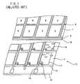
- FIG. 1is a schematic view illustrating a typical liquid crystal display (LCD) device.
- the LCD device 11includes upper and lower substrates 5 and 22 and an interposed liquid crystal material 14 .
- the upper substrate 5referred to as a color filter substrate, includes color filters 7 , a black matrix 6 and a transparent common electrode 18 formed on the color filter 7 .
- the color filter 7 and the black matrix 6are positioned in the same layer between the upper substrate 5 and the transparent common electrode 18 .
- the lower substrate 22referred to as an array substrate, includes pixel regions “P” defined by the gate and data lines 13 and 15 , pixel electrodes 17 formed on the pixel regions “P”, gate lines 13 arranged in a transverse direction, data lines 15 arranged in a perpendicular direction to the gate lines 13 , and thin film transistors (TFTs) “T” arranged near the crossing of the gate and data lines 13 and 15 in a matrix type.
- the pixel electrodes 17are made of a transparent conductive material such as ITO (indium-tin-oxide).
- ITOindium-tin-oxide
- the color filter layeris formed on the upper substrate and serves to display full color.
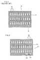
- FIG. 2is a schematic plan view illustrating a conventional color filter substrate.
- the color filter substrate 31comprises a transparent substrate (not shown), a black matrix 33 , an overcoat layer (not shown), a transparent common electrode (not shown) and color filters 35 that are red “R”, green “G” and blue “B”.
- the overcoat layeris formed between the color filters and the transparent common electrode.
- the component elements of the color filter substrateare optional in accordance with the LCD device type and operating mode.
- One pixel of the color filteris generally hundreds of square micrometers and a human being can not recognize it. Accordingly, the color filter is called a micro color filter.
- the color filters 35are formed from organic substances.
- the method of forming the color filters for use in a TFT-LCD deviceis classified into a dyeing method and a pigment dispersion method in accordance with the type of organic substance.
- the method of forming the color filtersis also classified into a dyeing method, a dispersion method, an electro-deposition method and a printing method.
- the pigment dispersion methodis most widely employed in fabricating the color filters.
- the black matrix 33is generally positioned between color filters 35 having red, green and blue colors.
- the black matrix 33includes portions corresponding to portions of the array substrate (see 22 of FIG. 1) that adhere to the color filter substrate when assembling the pair of substrates.
- the black matrix 33is also used for shielding the reverse tilted domain formed around the pixel electrode in an in-plane switching LCD device, for example.
- the black matrix 33shields the TFT (see “T” of FIG. 1) from the light to minimize leakage current in the TFT.
- a metal thin filmsuch as chrome having an optical density more than 3.5 and a carbon-base organic material are mainly used for the black matrix 33 .
- a double-layer black matrix, for example, chrome/chrome oxide (Cr/CrOx)is used to lower the reflection of the LCD device screen.
- the color filter substrate 31 described aboveis aligned and assembled with the array substrate (see element 22 of FIG. 1 ).
- alignment keysare formed on the color filter substrate and on the array substrate at the same position.
- the alignment key 37is formed on the color filter substrate 31 when patterning the black matrix 33 .
- the LCD devicewhen fabricating the LCD device with the color filter substrate 31 and the array substrate (see 22 of FIG. 1 ), information about the color filter such as the manufacturing company and/or the color filter type can not be identified after the scribing and cutting steps. If a defect is found in the color filter substrate, additional steps for confirming and identifying the color filter are thus required in order to send the color filter substrate back to the manufacturer. Accordingly, productivity becomes poor and the yield is lower.
- the color filter type among the various typesis chosen depending on the operation mode, and the color filter is not identified during the fabrication process of the LCD. If a wrong type of color filter is used, a complicated and labor intensive work is needed to confirm and identify the color filter after completing the LCD device.
- the present inventionis directed to a color filter substrate having an identification mark that substantially obviates one or more of the problems due to limitations and disadvantages of the related art.
- An advantage of the present inventionis a method of fabricating a color filter substrate having an identification mark for use in a liquid crystal display (LCD) device.
- a method of fabricating a color filter substrate for use in a liquid crystal display deviceincludes forming a black matrix on a substrate, the black matrix having a identification mark and an alignment key; forming patterns for color filters in the black matrix; and forming red, green and blue color filters in the patterns of the black matrix.
- the black matrixis made of chrome (Cr) or a resin including carbon.
- the identification markincludes a sign or a symbol such as characters or numbers.
- the signdenotes a manufacturer, a color filter type, a fabricating method and/or type of black matrix.
- the identification mark and the alignment keyare formed at periphery of the substrate.
- a color filter substrate for use in a liquid crystal display deviceincludes a substrate; a black matrix formed on the substrate; red, green and blue color filters; and an identification mark formed at a periphery of the substrate.
- the color filter substratefurther includes an alignment key formed at a periphery of the substrate.
- the identification markis formed by patterning the black matrix.
- a method of fabricating a liquid crystal display devicecomprises forming a black matrix on a first substrate, the black matrix having an identification mark at a periphery of the first substrate; forming a pattern in the black matrix corresponding to color filters; forming the color filters in the pattern of the black matrix; forming a transparent conductive layer over the color filters; and assembling the first substrate to a second substrate.
- FIG. 1is a schematic perspective view illustrating a conventional liquid crystal display device
- FIG. 2is a schematic plan view illustrating a conventional color filter substrate of a liquid crystal display device
- FIG. 3is a schematic plan view illustrating a color filter substrate according to a preferred embodiment of the present invention.
- FIGS. 4A and 4Bare schematic plan views illustrating process steps of fabricating the color filter substrate according the preferred embodiment of the present invention.
- FIG. 5Ais cross-sectional view of the color filters taken along line V—V of FIG. 4B;
- FIG. 5Bis a cross-sectional view of the identification mark and alignment key portions taken along line VI—VI of FIG. 4 B.
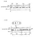
- FIG. 3is a plan view illustrating a color filter substrate according to a preferred embodiment of the present invention.
- the color filter substrate 211comprises a transparent substrate (not shown), a black matrix 213 , an overcoat layer (not shown), a transparent common electrode (not shown) and color filters 215 that are red “R”, green “G” and blue “B”.
- the color filter substrate 211includes portions that do not necessarily affect the image display.
- An alignment key 217 and an identification mark 219are preferably formed at portions that do not affect the image display.
- the identification mark 219has a sign “D810” which may represent information about the color filter as follows:
- the number “8”denotes the color filter type
- the number “1”denotes the fabricating method of the color filter
- the number “0”denotes the type of black matrix.
- the information about the color filtercan be checked and identified using the identification mark 219 .
- the identification mark 219can have many forms including a variety of different information.
- the identification mark 219is preferably simultaneously patterned when patterning the black matrix 213 .
- FIGS. 4A and 4Bschematically show steps of fabricating the color filter substrate according to the present invention.
- chrome oxide (CrO 2 ) and chrome (Cr)are preferably deposited on a transparent substrate 212 after cleaning the transparent substrate 212 .
- a resinsuch as a carbon-base organic material may also be used.
- the black matrix 213is formed by patterning the double-layer (Cr/CrO 2 ) or the resin, for example.
- color filter patterns 214are formed for the color filters in a later step. If chrome oxide (CrO 2 ) and chrome (Cr) are used, they are simultaneously etched by the etchant.
- the black matrix 213is related to the aperture ratio, the prevention of leakage current caused by the reflected light should be considered, and the assembly margin should also be considered when fabricating the LCD device.
- the black matrix 213usually corresponds to the TFT portion and to the gate and date line portions.
- the black matrix 213 covering the color filter patterns 214is removed such as by etching to open the color filter patterns 214 .
- the identification mark 219is also formed by patterning the portion of the black matrix 213 that does not affect the image display.
- the alignment key 217is also formed for aligning the color filter substrate 211 to the array substrate (see 22 of FIG. 1 ).
- the identification mark 219is used to store information about the color filter.
- FIG. 4Bshows a step of forming red, green and blue color filters 215 preferably using a photolithography process.
- the color resistis used as a photoresist.
- the red, green and blue color filters 215are simultaneously formed, respectively, using the mask process.
- the color resistis generally a negative photoresist in which the non-exposure portion is removed. Accordingly, the red, green and blue color filters 215 are formed by performing the photolithography process three times. Subsequently, an overcoat layer may be formed on the color filters and a transparent conductive material such as ITO (indium-tin-oxide) is deposited to form a transparent common electrode (see FIG. 5 A).
- ITOindium-tin-oxide
- FIG. 5Ashows a cross-sectional view of the RGB color filters in FIG. 4 B.
- color filters 215are formed separated by a black matrix 213 .
- an ITO layeris formed over the color filters 215 .
- An overcoat layermay be formed between the ITO layer and the color filter layer 215 .
- FIG. 5Bshows a cross-sectional view of the identification mark and the alignment key portions.
- the identification mark 219is “D810” preferably formed with the black matrix 213 .
- the alignment key 217is also preferably formed with the black matrix 213 .
- the manufacturer, the color filter type, the fabrication method and the type of black matrixare easily identified should a need arise, such as when a defect occurs in the color filter substrate, using the identification mark formed in the color filter substrate. Furthermore, the method of fabricating a color filter substrate of the present invention has the following advantages.
Landscapes
- Physics & Mathematics (AREA)
- Nonlinear Science (AREA)
- Mathematical Physics (AREA)
- Chemical & Material Sciences (AREA)
- Crystallography & Structural Chemistry (AREA)
- General Physics & Mathematics (AREA)
- Optics & Photonics (AREA)
- Optical Filters (AREA)
- Liquid Crystal (AREA)
Abstract
Description
Claims (23)
Applications Claiming Priority (2)
| Application Number | Priority Date | Filing Date | Title |
|---|---|---|---|
| KR1020000007714AKR100603842B1 (en) | 2000-02-18 | 2000-02-18 | Color filter including identification mark for confirmation |
| KR2000-7714 | 2000-02-18 |
Publications (2)
| Publication Number | Publication Date |
|---|---|
| US20010022637A1 US20010022637A1 (en) | 2001-09-20 |
| US6734931B2true US6734931B2 (en) | 2004-05-11 |
Family
ID=19647584
Family Applications (1)
| Application Number | Title | Priority Date | Filing Date |
|---|---|---|---|
| US09/785,456Expired - LifetimeUS6734931B2 (en) | 2000-02-18 | 2001-02-20 | Color filter substrate having identification mark formed in the black matrix |
Country Status (2)
| Country | Link |
|---|---|
| US (1) | US6734931B2 (en) |
| KR (1) | KR100603842B1 (en) |
Cited By (26)
| Publication number | Priority date | Publication date | Assignee | Title |
|---|---|---|---|---|
| US20030076572A1 (en)* | 2001-08-29 | 2003-04-24 | Seiko Epson Corporation | Electrooptical device and electronic equipment |
| US20030117549A1 (en)* | 2001-05-14 | 2003-06-26 | Lg. Philips Lcd Co., Ltd. | Color filter substrate having a panel identification and manufacturing method thereof |
| US20030117573A1 (en)* | 2001-12-24 | 2003-06-26 | Lg.Philips Lcd Co., Ltd. | Align key for a TOC/COT-type liquid crystal display device and method of fabricating the same |
| US20040125278A1 (en)* | 2002-12-31 | 2004-07-01 | Lg.Philips Lcd Co., Ltd. | Liquid crystal display device including color filter |
| US20040135937A1 (en)* | 2002-12-31 | 2004-07-15 | Dong-Ho Lee | Color filtering device for improved brightness |
| US20040228569A1 (en)* | 2002-06-04 | 2004-11-18 | Semiconductor Energy Laboratory Co., Ltd. | Product management method, program for performing product management, and storage medium having recorded the program therein |
| US20040263753A1 (en)* | 2003-06-30 | 2004-12-30 | Lg.Philips Lcd Co., Ltd. | In-plane switching mode liquid crystal display device and method of fabricating the same |
| US20040263709A1 (en)* | 2003-06-26 | 2004-12-30 | Samsung Electronics Co., Ltd. | Method of manufacturing thin film transistor array panel and liquid crystal display |
| US20050007327A1 (en)* | 2002-04-22 | 2005-01-13 | Cliff Elion | Color image display apparatus |
| US20050105017A1 (en)* | 2003-11-12 | 2005-05-19 | Lg.Philips Lcd Co., Ltd. | Liquid crystal display device and method for fabricating the same |
| US20060279687A1 (en)* | 2005-06-02 | 2006-12-14 | Park Kwang S | Liquid crystal display device |
| US20070025705A1 (en)* | 2005-07-12 | 2007-02-01 | Samsung Electronics Co., Ltd. | Mother panel substrate for display device and method of manufacturing the same |
| US20080261127A1 (en)* | 2007-04-20 | 2008-10-23 | Photronics, Inc. | Photomask with detector for optimizing an integrated circuit production process and method of manufacturing an integrated circuit using the same |
| US20080261123A1 (en)* | 2007-04-20 | 2008-10-23 | Photronics, Inc. | Photomask with detector for optimizing an integrated circuit production process and method of manufacturing an integrated circuit using the same |
| US20080261126A1 (en)* | 2007-04-20 | 2008-10-23 | Photronics, Inc. | Secure photomask with blocking aperture |
| US20080269379A1 (en)* | 2007-04-24 | 2008-10-30 | Belmont James A | Coating composition incorporating a low structure carbon black and devices formed therewith |
| US20100118252A1 (en)* | 2008-11-12 | 2010-05-13 | Au Optronics Corporation | Active device array substrate and liquid crystal display panel |
| US20120019764A1 (en)* | 2009-04-30 | 2012-01-26 | Sharp Kabushiki Kaisha | Method of manufacturing liquid crystal panel, glass substrate for liquid crystal panel, and liquid crystal panel including the same |
| US20130082907A1 (en)* | 2011-09-29 | 2013-04-04 | Korea University Research And Business Foundation | Display apparatus including a pattern and method for generating a |
| US20130229591A1 (en)* | 2012-03-02 | 2013-09-05 | Lg Display Co., Ltd. | Liquid crystal display device |
| US20150255022A1 (en)* | 2014-03-07 | 2015-09-10 | Samsung Display Co., Ltd. | Display device |
| US20170310859A1 (en)* | 2016-04-25 | 2017-10-26 | SK Hynix Inc. | Image sensor having outer and inner address markers |
| US9851597B2 (en)* | 2014-03-11 | 2017-12-26 | Samsung Display Co., Ltd. | Display panel including a verification code and display device having the same |
| US20180107037A1 (en)* | 2016-10-19 | 2018-04-19 | Samsung Display Co., Ltd. | Display device and related manufacturing method |
| US20230122068A1 (en)* | 2021-02-05 | 2023-04-20 | HKC Corporation Limited | Color filter substrate, method for manufacturing the same, and display panel |
| US12360415B2 (en)* | 2022-08-31 | 2025-07-15 | HKC Corporation Limited | Color filter substrate, method for manufacturing the same, and display panel |
Families Citing this family (25)
| Publication number | Priority date | Publication date | Assignee | Title |
|---|---|---|---|---|
| KR100752547B1 (en)* | 2000-12-29 | 2007-08-29 | 엘지.필립스 엘시디 주식회사 | Identity Mark and method for the same in Array Panel for Liquid Crystal Display Device |
| KR100801151B1 (en)* | 2001-10-04 | 2008-02-05 | 엘지.필립스 엘시디 주식회사 | Black Matrix for Liquid Crystal Display |
| KR100788732B1 (en)* | 2001-12-29 | 2007-12-26 | 엘지.필립스 엘시디 주식회사 | LCD Mask for Panel ID Titler |
| KR100790356B1 (en)* | 2001-12-29 | 2008-01-02 | 엘지.필립스 엘시디 주식회사 | Shift defect inspection method of color filter substrate for liquid crystal display |
| JP3838964B2 (en) | 2002-03-13 | 2006-10-25 | 株式会社リコー | Functional element substrate manufacturing equipment |
| KR100930495B1 (en)* | 2003-03-24 | 2009-12-09 | 삼성전자주식회사 | LCD Display |
| KR100993455B1 (en)* | 2003-12-30 | 2010-11-09 | 엘지디스플레이 주식회사 | Liquid crystal display device having ID mark and manufacturing method thereof |
| JP4502664B2 (en)* | 2004-02-24 | 2010-07-14 | 三洋電機株式会社 | Non-aqueous electrolyte secondary battery |
| KR101003829B1 (en)* | 2004-04-30 | 2010-12-23 | 엘지디스플레이 주식회사 | CIO structure liquid crystal display device and manufacturing method thereof |
| JP2006039298A (en)* | 2004-07-28 | 2006-02-09 | Mitsubishi Electric Corp | Liquid crystal display panel and liquid crystal display device using the same |
| KR101333864B1 (en) | 2004-10-21 | 2013-11-27 | 코닝 인코포레이티드 | Optical element with an opaque chrome coating having an aperture and method of making same |
| KR20060079721A (en)* | 2005-01-03 | 2006-07-06 | 삼성전자주식회사 | Manufacturing method of display panel for liquid crystal display device |
| KR100978259B1 (en)* | 2005-06-20 | 2010-08-26 | 엘지디스플레이 주식회사 | Liquid crystal panel cutting system and manufacturing method of liquid crystal display device using the same |
| KR100685903B1 (en)* | 2005-08-31 | 2007-02-26 | 동부일렉트로닉스 주식회사 | Manufacturing Method of Semiconductor Device |
| TWI269078B (en)* | 2005-12-30 | 2006-12-21 | Quanta Display Inc | Color filter substrate and fabricating method thereof |
| CN100380143C (en)* | 2006-02-22 | 2008-04-09 | 友达光电股份有限公司 | Color filter substrate and manufacturing method thereof |
| US8558977B2 (en)* | 2009-09-11 | 2013-10-15 | Apple Inc. | Electronic device display structures with alignment features |
| WO2012157601A1 (en)* | 2011-05-19 | 2012-11-22 | シャープ株式会社 | Liquid crystal display device |
| JP5856006B2 (en)* | 2012-04-27 | 2016-02-09 | 株式会社ジャパンディスプレイ | LCD panel |
| TWI476459B (en)* | 2012-05-03 | 2015-03-11 | Innocom Tech Shenzhen Co Ltd | A color filter substrate, and a touch screen display device |
| US20140098332A1 (en)* | 2012-10-10 | 2014-04-10 | Apple Inc. | Displays With Logos and Alignment Marks |
| JP2019191239A (en)* | 2018-04-19 | 2019-10-31 | シャープ株式会社 | Display panel |
| CN110764294B (en)* | 2019-06-11 | 2020-11-24 | 惠科股份有限公司 | Display panel and display device |
| CN110764305B (en)* | 2019-06-11 | 2020-12-25 | 惠科股份有限公司 | Display panel and display device |
| KR102231687B1 (en)* | 2020-07-06 | 2021-03-25 | 삼성디스플레이 주식회사 | Display panel and display apparatus having the same |
Citations (5)
| Publication number | Priority date | Publication date | Assignee | Title |
|---|---|---|---|---|
| US4343877A (en)* | 1981-01-02 | 1982-08-10 | Amdahl Corporation | System for design and production of integrated circuit photomasks and integrated circuit devices |
| JPH02210402A (en)* | 1989-02-10 | 1990-08-21 | Dainippon Printing Co Ltd | Color filter with identification mark |
| US5361150A (en) | 1990-07-19 | 1994-11-01 | Nec Corporation | Active matrix liquid crystal display with identification mark in the lower opaque conductive film |
| US5760421A (en)* | 1993-06-10 | 1998-06-02 | Canon Kabushiki Kaisha | Semiconductor device including indices for identifying positions of elements in the device. |
| US6597427B1 (en)* | 1999-07-06 | 2003-07-22 | International Business Machines Corporation | Liquid crystal panel, display device, identification mark detection device, detection display system, TFT array repair device and identification mark detection method |
- 2000
- 2000-02-18KRKR1020000007714Apatent/KR100603842B1/ennot_activeExpired - Fee Related
- 2001
- 2001-02-20USUS09/785,456patent/US6734931B2/ennot_activeExpired - Lifetime
Patent Citations (5)
| Publication number | Priority date | Publication date | Assignee | Title |
|---|---|---|---|---|
| US4343877A (en)* | 1981-01-02 | 1982-08-10 | Amdahl Corporation | System for design and production of integrated circuit photomasks and integrated circuit devices |
| JPH02210402A (en)* | 1989-02-10 | 1990-08-21 | Dainippon Printing Co Ltd | Color filter with identification mark |
| US5361150A (en) | 1990-07-19 | 1994-11-01 | Nec Corporation | Active matrix liquid crystal display with identification mark in the lower opaque conductive film |
| US5760421A (en)* | 1993-06-10 | 1998-06-02 | Canon Kabushiki Kaisha | Semiconductor device including indices for identifying positions of elements in the device. |
| US6597427B1 (en)* | 1999-07-06 | 2003-07-22 | International Business Machines Corporation | Liquid crystal panel, display device, identification mark detection device, detection display system, TFT array repair device and identification mark detection method |
Cited By (64)
| Publication number | Priority date | Publication date | Assignee | Title |
|---|---|---|---|---|
| US20060268205A1 (en)* | 2001-05-14 | 2006-11-30 | Lg Philips Lcd Co., Ltd. | Color filter substrate having a panel identification and manufacturing method thereof |
| US7102710B2 (en) | 2001-05-14 | 2006-09-05 | Lg.Philips Lcd Co., Ltd. | Manufacturing method of color filter substrate having panel identification |
| US7460197B2 (en)* | 2001-05-14 | 2008-12-02 | Lg Displays Co., Ltd. | Color filter substrate having a panel identification and manufacturing method thereof |
| US6914263B2 (en)* | 2001-05-14 | 2005-07-05 | Lg.Philips Lcd Co., Ltd. | Color filter substrate having a panel identification and manufacturing method thereof |
| US20050225702A1 (en)* | 2001-05-14 | 2005-10-13 | Lg Philips Lcd Co., Ltd. | Color filter substrate having a panel identification and manufacturing method thereof |
| US20030117549A1 (en)* | 2001-05-14 | 2003-06-26 | Lg. Philips Lcd Co., Ltd. | Color filter substrate having a panel identification and manufacturing method thereof |
| US20030076572A1 (en)* | 2001-08-29 | 2003-04-24 | Seiko Epson Corporation | Electrooptical device and electronic equipment |
| US8093656B2 (en) | 2001-08-29 | 2012-01-10 | Seiko Epson Corporation | Electrooptical device and electronic equipment having resin film in light emitting region and sealing region |
| US20080067595A1 (en)* | 2001-08-29 | 2008-03-20 | Seiko Epson Corporation | Electrooptical device and electronic equipment having resin film in light emitting region and sealing region |
| US7333167B2 (en)* | 2001-08-29 | 2008-02-19 | Seiko Epson Corporation | Electrooptical device and electronic equipment having resin film in light emitting region and sealing region |
| US20060274255A1 (en)* | 2001-12-24 | 2006-12-07 | Jong-Hoon Yi | Align key for a TOC/COT-type liquid crystal display device and method of fabricating the same |
| US7102724B2 (en)* | 2001-12-24 | 2006-09-05 | Lg.Philips Lcd.Co., Ltd. | Align key for a TOC/COT-type liquid crystal display device and method of fabricating the same |
| US7209210B2 (en) | 2001-12-24 | 2007-04-24 | Lg.Phillips Lcd Co., Ltd. | Align key for a TOC/COT-type liquid crystal display device and method of fabricating the same |
| US20030117573A1 (en)* | 2001-12-24 | 2003-06-26 | Lg.Philips Lcd Co., Ltd. | Align key for a TOC/COT-type liquid crystal display device and method of fabricating the same |
| US20050007327A1 (en)* | 2002-04-22 | 2005-01-13 | Cliff Elion | Color image display apparatus |
| US20040228569A1 (en)* | 2002-06-04 | 2004-11-18 | Semiconductor Energy Laboratory Co., Ltd. | Product management method, program for performing product management, and storage medium having recorded the program therein |
| US7239363B2 (en)* | 2002-12-31 | 2007-07-03 | Lg.Philips Lcd Co., Ltd | Liquid crystal display device including color filter |
| US20040125278A1 (en)* | 2002-12-31 | 2004-07-01 | Lg.Philips Lcd Co., Ltd. | Liquid crystal display device including color filter |
| US20040135937A1 (en)* | 2002-12-31 | 2004-07-15 | Dong-Ho Lee | Color filtering device for improved brightness |
| US7705936B2 (en)* | 2002-12-31 | 2010-04-27 | Samsung Electronics Co., Ltd. | Color filtering device for improved brightness |
| US7259807B2 (en)* | 2003-06-26 | 2007-08-21 | Samsung Electronics Co., Ltd. | Method of manufacturing thin film transistor array panel and liquid crystal display |
| US20040263709A1 (en)* | 2003-06-26 | 2004-12-30 | Samsung Electronics Co., Ltd. | Method of manufacturing thin film transistor array panel and liquid crystal display |
| US7126660B2 (en)* | 2003-06-30 | 2006-10-24 | Lg.Philips Lcd Co., Ltd. | In-plane switching mode liquid crystal display device including a black matrix with slit around the pixels and method of fabricating the same |
| US20040263753A1 (en)* | 2003-06-30 | 2004-12-30 | Lg.Philips Lcd Co., Ltd. | In-plane switching mode liquid crystal display device and method of fabricating the same |
| US7359014B2 (en)* | 2003-11-12 | 2008-04-15 | Lg.Philips Lcd Co., Ltd. | Liquid crystal display device and method for fabricating the same |
| US20050105017A1 (en)* | 2003-11-12 | 2005-05-19 | Lg.Philips Lcd Co., Ltd. | Liquid crystal display device and method for fabricating the same |
| US20060279687A1 (en)* | 2005-06-02 | 2006-12-14 | Park Kwang S | Liquid crystal display device |
| US7808608B2 (en)* | 2005-06-02 | 2010-10-05 | Lg. Display Co., Ltd. | Liquid crystal display device |
| US20070025705A1 (en)* | 2005-07-12 | 2007-02-01 | Samsung Electronics Co., Ltd. | Mother panel substrate for display device and method of manufacturing the same |
| US20100174393A1 (en)* | 2007-04-20 | 2010-07-08 | Christopher Progler | Photomask with detector for optimizing an integrated cirucit production process and method of manufacturing an integrated circuit using the same |
| US7851110B2 (en) | 2007-04-20 | 2010-12-14 | Photronics, Inc. | Secure photomask with blocking aperture |
| US20080261127A1 (en)* | 2007-04-20 | 2008-10-23 | Photronics, Inc. | Photomask with detector for optimizing an integrated circuit production process and method of manufacturing an integrated circuit using the same |
| US7943273B2 (en) | 2007-04-20 | 2011-05-17 | Photronics, Inc. | Photomask with detector for optimizing an integrated circuit production process and method of manufacturing an integrated circuit using the same |
| US20080261126A1 (en)* | 2007-04-20 | 2008-10-23 | Photronics, Inc. | Secure photomask with blocking aperture |
| US7790340B2 (en) | 2007-04-20 | 2010-09-07 | Photronics, Inc. | Photomask with detector for optimizing an integrated circuit production process and method of manufacturing an integrated circuit using the same |
| US20080261123A1 (en)* | 2007-04-20 | 2008-10-23 | Photronics, Inc. | Photomask with detector for optimizing an integrated circuit production process and method of manufacturing an integrated circuit using the same |
| US7910269B2 (en) | 2007-04-20 | 2011-03-22 | Photronics, Inc. | Photomask with detector for optimizing an integrated circuit production process and method of manufacturing an integrated circuit using the same |
| US8574537B2 (en) | 2007-04-24 | 2013-11-05 | Cabot Corporation | Low structure carbon black and method of making same |
| US20080269379A1 (en)* | 2007-04-24 | 2008-10-30 | Belmont James A | Coating composition incorporating a low structure carbon black and devices formed therewith |
| US9217944B2 (en) | 2007-04-24 | 2015-12-22 | Cabot Corporation | Low structure carbon black and method of making same |
| US20080292533A1 (en)* | 2007-04-24 | 2008-11-27 | Belmont James A | Low structure carbon black and method of making same |
| US8501148B2 (en) | 2007-04-24 | 2013-08-06 | Cabot Corporation | Coating composition incorporating a low structure carbon black and devices formed therewith |
| US20100118252A1 (en)* | 2008-11-12 | 2010-05-13 | Au Optronics Corporation | Active device array substrate and liquid crystal display panel |
| US8259276B2 (en)* | 2008-11-12 | 2012-09-04 | Au Optronics Corporation | Active device array substrate with plurality of marks in a peripheral area and liquid crystal display panel |
| US8582073B2 (en)* | 2009-04-30 | 2013-11-12 | Sharp Kabushiki Kaisha | Method of manufacturing liquid crystal panel, glass substrate for liquid crystal panel, and liquid crystal panel including the same |
| US20120019764A1 (en)* | 2009-04-30 | 2012-01-26 | Sharp Kabushiki Kaisha | Method of manufacturing liquid crystal panel, glass substrate for liquid crystal panel, and liquid crystal panel including the same |
| US20130082907A1 (en)* | 2011-09-29 | 2013-04-04 | Korea University Research And Business Foundation | Display apparatus including a pattern and method for generating a |
| US20130229591A1 (en)* | 2012-03-02 | 2013-09-05 | Lg Display Co., Ltd. | Liquid crystal display device |
| US9323119B2 (en)* | 2012-03-02 | 2016-04-26 | Lg Display Co., Ltd. | Liquid crystal display device |
| US20150255022A1 (en)* | 2014-03-07 | 2015-09-10 | Samsung Display Co., Ltd. | Display device |
| US9716111B2 (en)* | 2014-03-07 | 2017-07-25 | Samsung Display Co., Ltd. | Display device |
| US9851597B2 (en)* | 2014-03-11 | 2017-12-26 | Samsung Display Co., Ltd. | Display panel including a verification code and display device having the same |
| US9983430B2 (en) | 2014-03-11 | 2018-05-29 | Samsung Display Co., Ltd. | Display panel including a verification code and display device having the same |
| US10228583B2 (en) | 2014-03-11 | 2019-03-12 | Samsung Display Co., Ltd. | Display panel including a verification code and display device having the same |
| CN107305900A (en)* | 2016-04-25 | 2017-10-31 | 爱思开海力士有限公司 | Imaging sensor with outwardly and inwardly address mark |
| US20170310859A1 (en)* | 2016-04-25 | 2017-10-26 | SK Hynix Inc. | Image sensor having outer and inner address markers |
| US10356293B2 (en)* | 2016-04-25 | 2019-07-16 | SK Hynix Inc. | Image sensor having outer and inner address markers |
| CN107305900B (en)* | 2016-04-25 | 2021-01-08 | 爱思开海力士有限公司 | Image sensor with external and internal address marking |
| US20180107037A1 (en)* | 2016-10-19 | 2018-04-19 | Samsung Display Co., Ltd. | Display device and related manufacturing method |
| US10067388B2 (en)* | 2016-10-19 | 2018-09-04 | Samsung Display Co., Ltd. | Display device and related manufacturing method |
| US10663811B2 (en) | 2016-10-19 | 2020-05-26 | Samsung Display Co., Ltd. | Display device and related manufacturing method |
| US20230122068A1 (en)* | 2021-02-05 | 2023-04-20 | HKC Corporation Limited | Color filter substrate, method for manufacturing the same, and display panel |
| US11982895B2 (en)* | 2021-02-05 | 2024-05-14 | HKC Corporation Limited | Color filter substrate, method for manufacturing the same, and display panel |
| US12360415B2 (en)* | 2022-08-31 | 2025-07-15 | HKC Corporation Limited | Color filter substrate, method for manufacturing the same, and display panel |
Also Published As
| Publication number | Publication date |
|---|---|
| KR20010081676A (en) | 2001-08-29 |
| US20010022637A1 (en) | 2001-09-20 |
| KR100603842B1 (en) | 2006-07-24 |
Similar Documents
| Publication | Publication Date | Title |
|---|---|---|
| US6734931B2 (en) | Color filter substrate having identification mark formed in the black matrix | |
| US6803975B2 (en) | Liquid crystal display panel and manufacturing method thereof | |
| JP4775836B2 (en) | Display device and manufacturing method thereof | |
| US7423710B2 (en) | Color filter panel and its fabrication method using back exposure | |
| KR100353167B1 (en) | Liquid Crystal Display Device and Method for Fabricating the Same | |
| US20070188670A1 (en) | LCD array substrate and fabrication method thereof | |
| US20040125261A1 (en) | Array substrate for LCD and method of fabricating the same | |
| US20080136993A1 (en) | Method of Forming a Cell Identification, Display Substrate and Display Device Having the Same | |
| US7545466B2 (en) | Liquid crystal display device and substrate therefor | |
| JP2000029014A (en) | Color filter substrate for liquid crystal display device and liquid crystal display device | |
| US7906782B2 (en) | Liquid crystal display device | |
| US7359014B2 (en) | Liquid crystal display device and method for fabricating the same | |
| US20020140893A1 (en) | Method for fabricating a spacer for liquid crystal display | |
| KR100271706B1 (en) | An active matrix type liquid crystal display and a methd for manufacturing thereof0 | |
| CN106918948B (en) | Method for manufacturing color resistor | |
| JP2000098126A (en) | Manufacturing method of color filter | |
| JP2000098128A (en) | Color filter | |
| JPH0720310A (en) | Liquid crystal element manufacturing method | |
| JP4493374B2 (en) | Color filter substrate manufacturing method, color filter substrate inspection method, and liquid crystal display device manufacturing method | |
| KR20070002925A (en) | Short defective repair method and manufacturing method of liquid crystal display device using the same | |
| KR101604271B1 (en) | In plane switching mode liquid crystal display device and method of fabricating the same | |
| CN107065281B (en) | Method for manufacturing color resistor | |
| KR101089097B1 (en) | Color filter substrate and liquid crystal display device using the same | |
| KR20060134760A (en) | LCD panel and manufacturing method | |
| KR100400163B1 (en) | Method for manufacturing low reflection color filter substrate |
Legal Events
| Date | Code | Title | Description |
|---|---|---|---|
| AS | Assignment | Owner name:KASAI KOGYO CO., LTD., JAPAN Free format text:ASSIGNMENT OF ASSIGNORS INTEREST;ASSIGNOR:HAGAI, TATSURO;REEL/FRAME:011559/0618 Effective date:20010214 | |
| AS | Assignment | Owner name:LG.PHILIPS LCD CO., LTD., KOREA, REPUBLIC OF Free format text:ASSIGNMENT OF ASSIGNORS INTEREST;ASSIGNOR:YU, HWAN-SEONG;REEL/FRAME:011740/0039 Effective date:20010216 | |
| FEPP | Fee payment procedure | Free format text:PAYER NUMBER DE-ASSIGNED (ORIGINAL EVENT CODE: RMPN); ENTITY STATUS OF PATENT OWNER: LARGE ENTITY Free format text:PAYOR NUMBER ASSIGNED (ORIGINAL EVENT CODE: ASPN); ENTITY STATUS OF PATENT OWNER: LARGE ENTITY | |
| STCF | Information on status: patent grant | Free format text:PATENTED CASE | |
| FPAY | Fee payment | Year of fee payment:4 | |
| AS | Assignment | Owner name:LG DISPLAY CO., LTD., KOREA, REPUBLIC OF Free format text:CHANGE OF NAME;ASSIGNOR:LG.PHILIPS LCD CO., LTD.;REEL/FRAME:021763/0177 Effective date:20080304 Owner name:LG DISPLAY CO., LTD.,KOREA, REPUBLIC OF Free format text:CHANGE OF NAME;ASSIGNOR:LG.PHILIPS LCD CO., LTD.;REEL/FRAME:021763/0177 Effective date:20080304 | |
| FEPP | Fee payment procedure | Free format text:PAYER NUMBER DE-ASSIGNED (ORIGINAL EVENT CODE: RMPN); ENTITY STATUS OF PATENT OWNER: LARGE ENTITY Free format text:PAYOR NUMBER ASSIGNED (ORIGINAL EVENT CODE: ASPN); ENTITY STATUS OF PATENT OWNER: LARGE ENTITY | |
| FPAY | Fee payment | Year of fee payment:8 | |
| FPAY | Fee payment | Year of fee payment:12 |