US6734107B2 - Pitch reduction in semiconductor fabrication - Google Patents
Pitch reduction in semiconductor fabricationDownload PDFInfo
- Publication number
- US6734107B2 US6734107B2US10/170,308US17030802AUS6734107B2US 6734107 B2US6734107 B2US 6734107B2US 17030802 AUS17030802 AUS 17030802AUS 6734107 B2US6734107 B2US 6734107B2
- Authority
- US
- United States
- Prior art keywords
- layer
- conductive layer
- conductive
- forming
- photoresist
- Prior art date
- Legal status (The legal status is an assumption and is not a legal conclusion. Google has not performed a legal analysis and makes no representation as to the accuracy of the status listed.)
- Expired - Lifetime, expires
Links
- 238000004519manufacturing processMethods0.000titledescription8
- 239000004065semiconductorSubstances0.000titledescription5
- 229910021420polycrystalline siliconInorganic materials0.000claimsabstractdescription67
- 229920005591polysiliconPolymers0.000claimsabstractdescription66
- 238000000034methodMethods0.000claimsabstractdescription62
- 229920002120photoresistant polymerPolymers0.000claimsabstractdescription52
- 229920000642polymerPolymers0.000claimsabstractdescription37
- 239000000758substrateSubstances0.000claimsabstractdescription36
- 238000005530etchingMethods0.000claimsabstractdescription20
- 238000000206photolithographyMethods0.000claimsabstractdescription16
- VYPSYNLAJGMNEJ-UHFFFAOYSA-NSilicium dioxideChemical compoundO=[Si]=OVYPSYNLAJGMNEJ-UHFFFAOYSA-N0.000claimsdescription16
- XUIMIQQOPSSXEZ-UHFFFAOYSA-NSiliconChemical compound[Si]XUIMIQQOPSSXEZ-UHFFFAOYSA-N0.000claimsdescription12
- 229910052710siliconInorganic materials0.000claimsdescription12
- 239000010703siliconSubstances0.000claimsdescription12
- 229910052581Si3N4Inorganic materials0.000claimsdescription5
- HQVNEWCFYHHQES-UHFFFAOYSA-Nsilicon nitrideChemical compoundN12[Si]34N5[Si]62N3[Si]51N64HQVNEWCFYHHQES-UHFFFAOYSA-N0.000claimsdescription5
- 238000001312dry etchingMethods0.000claimsdescription3
- 229910052814silicon oxideInorganic materials0.000claimsdescription3
- 238000005498polishingMethods0.000claimsdescription2
- 230000010354integrationEffects0.000abstractdescription4
- 239000004020conductorSubstances0.000description29
- 239000000463materialSubstances0.000description13
- 239000002019doping agentSubstances0.000description9
- 238000005229chemical vapour depositionMethods0.000description8
- 230000005855radiationEffects0.000description8
- 239000000377silicon dioxideSubstances0.000description6
- BLRPTPMANUNPDV-UHFFFAOYSA-NSilaneChemical compound[SiH4]BLRPTPMANUNPDV-UHFFFAOYSA-N0.000description5
- 238000006243chemical reactionMethods0.000description5
- 239000003989dielectric materialSubstances0.000description5
- 230000003287optical effectEffects0.000description5
- QGZKDVFQNNGYKY-UHFFFAOYSA-NAmmoniaChemical compoundNQGZKDVFQNNGYKY-UHFFFAOYSA-N0.000description4
- GQPLMRYTRLFLPF-UHFFFAOYSA-NNitrous OxideChemical compound[O-][N+]#NGQPLMRYTRLFLPF-UHFFFAOYSA-N0.000description4
- 239000011248coating agentSubstances0.000description4
- 238000000576coating methodMethods0.000description4
- 239000007789gasSubstances0.000description4
- TXEYQDLBPFQVAA-UHFFFAOYSA-NtetrafluoromethaneChemical groupFC(F)(F)FTXEYQDLBPFQVAA-UHFFFAOYSA-N0.000description4
- KRHYYFGTRYWZRS-UHFFFAOYSA-NFluoraneChemical compoundFKRHYYFGTRYWZRS-UHFFFAOYSA-N0.000description3
- 230000015572biosynthetic processEffects0.000description3
- 239000003795chemical substances by applicationSubstances0.000description3
- 230000004048modificationEffects0.000description3
- 238000012986modificationMethods0.000description3
- XKRFYHLGVUSROY-UHFFFAOYSA-NArgonChemical compound[Ar]XKRFYHLGVUSROY-UHFFFAOYSA-N0.000description2
- MYMOFIZGZYHOMD-UHFFFAOYSA-NDioxygenChemical compoundO=OMYMOFIZGZYHOMD-UHFFFAOYSA-N0.000description2
- 238000000151depositionMethods0.000description2
- 230000008021depositionEffects0.000description2
- 229910001882dioxygenInorganic materials0.000description2
- 229910000069nitrogen hydrideInorganic materials0.000description2
- 239000001272nitrous oxideSubstances0.000description2
- 230000003647oxidationEffects0.000description2
- 238000007254oxidation reactionMethods0.000description2
- 238000000059patterningMethods0.000description2
- 235000012239silicon dioxideNutrition0.000description2
- 239000007787solidSubstances0.000description2
- 238000012876topographyMethods0.000description2
- JBRZTFJDHDCESZ-UHFFFAOYSA-NAsGaChemical compound[As]#[Ga]JBRZTFJDHDCESZ-UHFFFAOYSA-N0.000description1
- IJGRMHOSHXDMSA-UHFFFAOYSA-NAtomic nitrogenChemical compoundN#NIJGRMHOSHXDMSA-UHFFFAOYSA-N0.000description1
- ZOXJGFHDIHLPTG-UHFFFAOYSA-NBoronChemical compound[B]ZOXJGFHDIHLPTG-UHFFFAOYSA-N0.000description1
- JMASRVWKEDWRBT-UHFFFAOYSA-NGallium nitrideChemical compound[Ga]#NJMASRVWKEDWRBT-UHFFFAOYSA-N0.000description1
- UFHFLCQGNIYNRP-UHFFFAOYSA-NHydrogenChemical compound[H][H]UFHFLCQGNIYNRP-UHFFFAOYSA-N0.000description1
- CPELXLSAUQHCOX-UHFFFAOYSA-NHydrogen bromideChemical compoundBrCPELXLSAUQHCOX-UHFFFAOYSA-N0.000description1
- OAICVXFJPJFONN-UHFFFAOYSA-NPhosphorusChemical compound[P]OAICVXFJPJFONN-UHFFFAOYSA-N0.000description1
- 230000002411adverseEffects0.000description1
- 229910021529ammoniaInorganic materials0.000description1
- 229910052787antimonyInorganic materials0.000description1
- WATWJIUSRGPENY-UHFFFAOYSA-Nantimony atomChemical compound[Sb]WATWJIUSRGPENY-UHFFFAOYSA-N0.000description1
- 229910052786argonInorganic materials0.000description1
- 229910052785arsenicInorganic materials0.000description1
- RQNWIZPPADIBDY-UHFFFAOYSA-Narsenic atomChemical compound[As]RQNWIZPPADIBDY-UHFFFAOYSA-N0.000description1
- QVGXLLKOCUKJST-UHFFFAOYSA-Natomic oxygenChemical group[O]QVGXLLKOCUKJST-UHFFFAOYSA-N0.000description1
- 229910052796boronInorganic materials0.000description1
- 239000008119colloidal silicaSubstances0.000description1
- 238000007796conventional methodMethods0.000description1
- 229910021419crystalline siliconInorganic materials0.000description1
- 238000000354decomposition reactionMethods0.000description1
- BUMGIEFFCMBQDG-UHFFFAOYSA-NdichlorosiliconChemical compoundCl[Si]ClBUMGIEFFCMBQDG-UHFFFAOYSA-N0.000description1
- OKZIUSOJQLYFSE-UHFFFAOYSA-NdifluoroboronChemical compoundF[B]FOKZIUSOJQLYFSE-UHFFFAOYSA-N0.000description1
- RWRIWBAIICGTTQ-UHFFFAOYSA-NdifluoromethaneChemical compoundFCFRWRIWBAIICGTTQ-UHFFFAOYSA-N0.000description1
- 229910001873dinitrogenInorganic materials0.000description1
- 230000009977dual effectEffects0.000description1
- 230000000694effectsEffects0.000description1
- 239000011521glassSubstances0.000description1
- 238000010438heat treatmentMethods0.000description1
- 239000012535impuritySubstances0.000description1
- 238000011065in-situ storageMethods0.000description1
- 239000011810insulating materialSubstances0.000description1
- 238000010849ion bombardmentMethods0.000description1
- QPJSUIGXIBEQAC-UHFFFAOYSA-Nn-(2,4-dichloro-5-propan-2-yloxyphenyl)acetamideChemical compoundCC(C)OC1=CC(NC(C)=O)=C(Cl)C=C1ClQPJSUIGXIBEQAC-UHFFFAOYSA-N0.000description1
- 239000012811non-conductive materialSubstances0.000description1
- 239000001301oxygenSubstances0.000description1
- 229910052760oxygenInorganic materials0.000description1
- 229910052698phosphorusInorganic materials0.000description1
- 239000011574phosphorusSubstances0.000description1
- 238000006552photochemical reactionMethods0.000description1
- 229910000077silaneInorganic materials0.000description1
- 239000002002slurrySubstances0.000description1
- 239000002904solventSubstances0.000description1
- 239000000126substanceSubstances0.000description1
- 239000000725suspensionSubstances0.000description1
Images


Classifications
- H—ELECTRICITY
- H01—ELECTRIC ELEMENTS
- H01L—SEMICONDUCTOR DEVICES NOT COVERED BY CLASS H10
- H01L21/00—Processes or apparatus adapted for the manufacture or treatment of semiconductor or solid state devices or of parts thereof
- H01L21/02—Manufacture or treatment of semiconductor devices or of parts thereof
- H01L21/027—Making masks on semiconductor bodies for further photolithographic processing not provided for in group H01L21/18 or H01L21/34
- H01L21/033—Making masks on semiconductor bodies for further photolithographic processing not provided for in group H01L21/18 or H01L21/34 comprising inorganic layers
- H01L21/0334—Making masks on semiconductor bodies for further photolithographic processing not provided for in group H01L21/18 or H01L21/34 comprising inorganic layers characterised by their size, orientation, disposition, behaviour, shape, in horizontal or vertical plane
- H01L21/0337—Making masks on semiconductor bodies for further photolithographic processing not provided for in group H01L21/18 or H01L21/34 comprising inorganic layers characterised by their size, orientation, disposition, behaviour, shape, in horizontal or vertical plane characterised by the process involved to create the mask, e.g. lift-off masks, sidewalls, or to modify the mask, e.g. pre-treatment, post-treatment
- H—ELECTRICITY
- H01—ELECTRIC ELEMENTS
- H01L—SEMICONDUCTOR DEVICES NOT COVERED BY CLASS H10
- H01L21/00—Processes or apparatus adapted for the manufacture or treatment of semiconductor or solid state devices or of parts thereof
- H01L21/02—Manufacture or treatment of semiconductor devices or of parts thereof
- H01L21/027—Making masks on semiconductor bodies for further photolithographic processing not provided for in group H01L21/18 or H01L21/34
- H01L21/033—Making masks on semiconductor bodies for further photolithographic processing not provided for in group H01L21/18 or H01L21/34 comprising inorganic layers
- H01L21/0334—Making masks on semiconductor bodies for further photolithographic processing not provided for in group H01L21/18 or H01L21/34 comprising inorganic layers characterised by their size, orientation, disposition, behaviour, shape, in horizontal or vertical plane
- H01L21/0338—Process specially adapted to improve the resolution of the mask
- H—ELECTRICITY
- H01—ELECTRIC ELEMENTS
- H01L—SEMICONDUCTOR DEVICES NOT COVERED BY CLASS H10
- H01L21/00—Processes or apparatus adapted for the manufacture or treatment of semiconductor or solid state devices or of parts thereof
- H01L21/02—Manufacture or treatment of semiconductor devices or of parts thereof
- H01L21/04—Manufacture or treatment of semiconductor devices or of parts thereof the devices having potential barriers, e.g. a PN junction, depletion layer or carrier concentration layer
- H01L21/18—Manufacture or treatment of semiconductor devices or of parts thereof the devices having potential barriers, e.g. a PN junction, depletion layer or carrier concentration layer the devices having semiconductor bodies comprising elements of Group IV of the Periodic Table or AIIIBV compounds with or without impurities, e.g. doping materials
- H01L21/28—Manufacture of electrodes on semiconductor bodies using processes or apparatus not provided for in groups H01L21/20 - H01L21/268
- H01L21/28008—Making conductor-insulator-semiconductor electrodes
- H01L21/28017—Making conductor-insulator-semiconductor electrodes the insulator being formed after the semiconductor body, the semiconductor being silicon
- H01L21/28026—Making conductor-insulator-semiconductor electrodes the insulator being formed after the semiconductor body, the semiconductor being silicon characterised by the conductor
- H01L21/28123—Lithography-related aspects, e.g. sub-lithography lengths; Isolation-related aspects, e.g. to solve problems arising at the crossing with the side of the device isolation; Planarisation aspects
- H—ELECTRICITY
- H01—ELECTRIC ELEMENTS
- H01L—SEMICONDUCTOR DEVICES NOT COVERED BY CLASS H10
- H01L21/00—Processes or apparatus adapted for the manufacture or treatment of semiconductor or solid state devices or of parts thereof
- H01L21/02—Manufacture or treatment of semiconductor devices or of parts thereof
- H01L21/04—Manufacture or treatment of semiconductor devices or of parts thereof the devices having potential barriers, e.g. a PN junction, depletion layer or carrier concentration layer
- H01L21/18—Manufacture or treatment of semiconductor devices or of parts thereof the devices having potential barriers, e.g. a PN junction, depletion layer or carrier concentration layer the devices having semiconductor bodies comprising elements of Group IV of the Periodic Table or AIIIBV compounds with or without impurities, e.g. doping materials
- H01L21/30—Treatment of semiconductor bodies using processes or apparatus not provided for in groups H01L21/20 - H01L21/26
- H01L21/31—Treatment of semiconductor bodies using processes or apparatus not provided for in groups H01L21/20 - H01L21/26 to form insulating layers thereon, e.g. for masking or by using photolithographic techniques; After treatment of these layers; Selection of materials for these layers
- H01L21/3205—Deposition of non-insulating-, e.g. conductive- or resistive-, layers on insulating layers; After-treatment of these layers
- H01L21/321—After treatment
- H01L21/3213—Physical or chemical etching of the layers, e.g. to produce a patterned layer from a pre-deposited extensive layer
- H01L21/32139—Physical or chemical etching of the layers, e.g. to produce a patterned layer from a pre-deposited extensive layer using masks
- H—ELECTRICITY
- H01—ELECTRIC ELEMENTS
- H01L—SEMICONDUCTOR DEVICES NOT COVERED BY CLASS H10
- H01L21/00—Processes or apparatus adapted for the manufacture or treatment of semiconductor or solid state devices or of parts thereof
- H01L21/02—Manufacture or treatment of semiconductor devices or of parts thereof
- H01L21/04—Manufacture or treatment of semiconductor devices or of parts thereof the devices having potential barriers, e.g. a PN junction, depletion layer or carrier concentration layer
- H01L21/18—Manufacture or treatment of semiconductor devices or of parts thereof the devices having potential barriers, e.g. a PN junction, depletion layer or carrier concentration layer the devices having semiconductor bodies comprising elements of Group IV of the Periodic Table or AIIIBV compounds with or without impurities, e.g. doping materials
- H01L21/30—Treatment of semiconductor bodies using processes or apparatus not provided for in groups H01L21/20 - H01L21/26
- H01L21/31—Treatment of semiconductor bodies using processes or apparatus not provided for in groups H01L21/20 - H01L21/26 to form insulating layers thereon, e.g. for masking or by using photolithographic techniques; After treatment of these layers; Selection of materials for these layers
- H01L21/3205—Deposition of non-insulating-, e.g. conductive- or resistive-, layers on insulating layers; After-treatment of these layers
- H01L21/321—After treatment
- H01L21/3213—Physical or chemical etching of the layers, e.g. to produce a patterned layer from a pre-deposited extensive layer
- H01L21/32133—Physical or chemical etching of the layers, e.g. to produce a patterned layer from a pre-deposited extensive layer by chemical means only
- H01L21/32135—Physical or chemical etching of the layers, e.g. to produce a patterned layer from a pre-deposited extensive layer by chemical means only by vapour etching only
- H01L21/32136—Physical or chemical etching of the layers, e.g. to produce a patterned layer from a pre-deposited extensive layer by chemical means only by vapour etching only using plasmas
- H01L21/32137—Physical or chemical etching of the layers, e.g. to produce a patterned layer from a pre-deposited extensive layer by chemical means only by vapour etching only using plasmas of silicon-containing layers
Definitions
- the present inventionrelates generally to semiconductor fabrication methods and, more particularly, to methods for fabricating transistor devices having a reduced pitch.
- Modern integrated circuitscontain numerous structures that comprise conductive material, semi-conductive material (i.e., rendered conductive in defined areas with dopants), and/or non-conductive material.
- transistor devicesare commonly fabricated by forming a semi-conductive material, such as polycrystalline silicon (polysilicon) over a relatively thin gate dielectric arranged upon a semiconductor substrate.
- the polysilicon materialis patterned to define gate conductors spaced laterally apart above the substrate.
- exposed regions of the substrateare implanted with impurity dopants to form source/drain junctions in the substrate between the gate conductors. If the dopant species employed for forming the source/drain regions is n-type, then an NMOSFET (n-channel) transistor device is formed.
- CMOSFETp-channel transistor device
- Transistor gate conductorsare defined using a technique known as photolithography.
- a photosensitive filmi.e., photoresist
- An optical imageis transferred to the photoresist by projecting a form of radiation, typically ultraviolet light, through the transparent portions of a mask plate.
- a photochemical reactionalters the solubility of the regions of the photoresist exposed to the radiation.
- the photoresistis washed with a solvent known as developer to preferentially remove the regions of higher solubility, followed by curing the remaining regions of the photoresist. Those remaining regions of the photoresist are highly resistant to attack by an etching agent that is capable of removing the polysilicon material.
- the portions of the polysilicon left exposed by the photoresistare etched away to define gate conductors of ensuing transistor devices.
- the minimum lateral dimension that can be achieved for a patterned photoresist featureis limited by, among other things, the resolution of the optical system used to project the image onto the photoresist.
- resolutiondescribes the ability of an optical system to distinguish closely spaced objects. Diffraction effects may undesirably occur as the radiation passes through slit-like transparent regions of the mask plate, scattering the radiation and therefore adversely affecting the resolution of the optical system.
- the photoresist regions exposed to the radiationfail to correspond to the mask plate pattern, resulting in the photoresist features being skewed. Consequently, the photolithography process limits the minimum achievable widths of the features of a conventional integrated circuit. It is therefore difficult to reduce the widths of and distances between for example transistor gate conductors, which are defined by the photolithography process.
- the pitch of for example transistor devices formed with conventional methodscannot be easily reduced.
- the “pitch”is herein defined as the distance between the same points of two adjacent structures of the same type, e.g., two adjacent gate conductors. Since the pitch of the devices cannot be easily reduced, the device integration cannot be increased to meet the high demand for smaller and faster integrated circuits.
- the present inventionaddresses these needs by providing a method for forming transistor devices having a reduced pitch.
- the pitch of the formed devicescan be reduced to, e.g., half that of conventional devices, by using current photolithography conditions. Since the pitch of the devices can be reduced, the device integration can be increased, resulting in smaller and faster integrated circuits.
- a conductive layer, a stop layer, and a polysilicon layerare formed on a substrate.
- a patterned photoresist layeris formed on the polysilicon layer, and a first polymer layer is formed on surfaces of the photoresist layer.
- the first polymer layeris used as an etching mask to define the polysilicon layer, the stop layer, and the conductive layer.
- An oxide layeris formed on the substrate, and then the oxide layer is etched back until the polysilicon layer is exposed.
- the polysilicon layeris removed, and a second polymer layer is formed on surfaces of the oxide layer.
- the second polymer layeris used as an etching mask to define the conductive layer. Then, the second polymer layer is removed.
- transistorsare formed using several process steps.
- a first conductive layer, a stop layer, and a second conductive layerare consecutively deposited on a semiconductor substrate.
- the first and second conductive layersmay be composed of a conductive or semi-conductive material and are preferably composed of polysilicon.
- the stop layermay be a dielectric material having an etch rate less than an etch rate of the second conductive layer when using an etching agent (i.e., etchant) that is highly selective to the second conductive layer. If, for example, the conductive layers comprise polysilicon, the stop layer may be silicon nitride or silicon oxy-nitride.
- a photoresist layeris patterned on the second conductive layer using the photolithography process.
- a first dielectric layeris then selectively formed on surfaces of the photoresist layer.
- the first dielectric layermay be composed of a polymer created in an etcher using the dielectric resolution enhancement coating technique.
- the first conductive layer, the stop layer, and the second conductive layerare defined using the first dielectric layer as an etching mask. Having served their purpose, the photoresist layer and the first dielectric layer are then removed.
- an insulating layeris deposited on the substrate to a level above the second conductive layer.
- the insulating layermay be composed of an oxide, e.g., a spin on glass (SOG) oxide, such that its etch rate is less than the etch rate of the second conductive layer when an etchant that is highly selective to the second conductive layer is used.
- SOGspin on glass
- the insulating layeris then removed down to the upper surface of the second conductive layer, thereby exposing the second conductive layer.
- a dry etching process or a chemical-mechanical polishing (CMP) processmay be employed to remove the insulating layer.
- the second conductive layeris then removed to expose the stop layer, followed by forming a second dielectric layer, e.g., a polymer, on surfaces of the insulating layer to serve as an etch mask.
- a second dielectric layere.g., a polymer
- the dielectric resolution enhancement coating techniquewhich can be performed in an etcher, may be used to form the second dielectric layer.
- portions of the stop layer and first conductive layer not covered by the second dielectric layermay be removed.
- the second dielectric layeris removed, leaving behind a plurality of gate conductors that are laterally spaced apart on a substrate, and an etch stop material positioned over the gate conductors.
- a gate dielectricis interposed between the substrate and the plurality of gate conductors.
- Transistor devicesmay be subsequently formed by implanting dopants into source/drain regions of the substrate located between the gate conductors.
- a lateral width of each gate conductoris substantially less than a lateral width of a feature of a conventional, patterned photoresist layer.
- a pitch of the plurality of gate conductorsis substantially less than a pitch of features of a conventional, patterned photoresist layer. The resulting pitch of the transistor devices fabricated according to this method is significantly reduced compared to the pitch of conventional transistor devices.
- FIG. 1is a cross-sectional view of a prior art silicon substrate upon which gate oxide layer and a polysilicon layer has been formed, wherein a photoresist layer is patterned upon the polysilicon layer in accordance with a conventional fabrication method;
- FIG. 2is a cross-sectional view of the prior-art configuration depicted in FIG. 1, wherein the polysilicon layer is defined using the photoresist layer as an etch mask;
- FIG. 3is a cross-sectional view of a silicon substrate upon which a gate oxide layer/first polysilicon layer/stop layer/second polysilicon layer film stack has been formed, wherein a photoresist layer is patterned upon the film stack in accordance with a preferred embodiment of the invention;
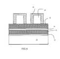
- FIG. 4is a cross-sectional view of the configuration depicted in FIG. 3, wherein a first polymer layer is formed on surfaces of the photoresist layer in accordance with a preferred embodiment of the invention
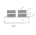
- FIG. 5is a cross-sectional view of the configuration depicted in FIG. 4, wherein the first polysilicon layer, the stop layer, and the second polysilicon layer are defined using the first polymer layer as an etch mask in accordance with a preferred embodiment of the invention;
- FIG. 6is a cross-sectional view of the configuration depicted in FIG. 5, wherein an oxide layer is formed on the substrate in accordance with a preferred embodiment of the invention
- FIG. 7is a cross-sectional view of the configuration depicted in FIG. 6, wherein the oxide layer is removed down to the upper surface of the second polysilicon layer in accordance with a preferred embodiment of the invention
- FIG. 8is a cross-sectional view of the configuration depicted in FIG. 7, wherein the second polysilicon layer is removed to expose the stop layer in accordance with a preferred embodiment of the invention
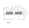
- FIG. 9is a cross-sectional view of the configuration depicted in FIG. 8, wherein a second polymer layer is formed on the surfaces of the oxide layer in accordance with a preferred embodiment of the invention.
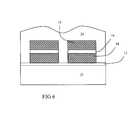
- FIG. 10is a cross-sectional view of the configuration depicted in FIG. 9, wherein the first polysilicon layer and the stop layer are defined using the second polymer layer as an etching mask.
- the fabrication method in accordance with the present inventionincludes selectively etching a conductive polysilicon layer that has a selectivity to an etchant that is greater than the selectivity (to the same etchant) of an underlying stop layer.
- FIGS. 1 and 2illustrate a prior-art fabrication method used to form gate conductors of transistor devices.
- a gate oxide layer 4comprising silicon dioxide (SiO 2 ) is formed on a silicon substrate 2 .
- the relatively thin gate oxide layer 4is thermally grown at the surface of substrate 2 by heating the substrate while exposing it to oxygen gas.
- Polysilicon layer 6is formed across gate oxide layer 4 using chemical vapor deposition (CVD) from a silane (SiH 4 ) source.
- CVDchemical vapor deposition
- SiH 4silane
- the photolithography process described aboveis then used to pattern photoresist layer 8 on polysilicon layer 6 .
- Drawbacks of the photolithography processlimit the minimum dimension that can be achieved for the features of photoresist layer 8 .
- an etch techniquesuch as a dry, plasma etch is performed to remove portions of polysilicon layer 6 not covered by photoresist layer 8 .
- Photoresist layer 8is highly resistant to attack by the etchant, which is highly selective to polysilicon. As such, photoresist layer 8 acts as an etching mask during the patterning of polysilicon layer 6 .
- gate conductorsare defined in polysilicon layer 6 that have widths approximately equal to the widths of the overlying photoresist features.
- Photoresist layer 8is stripped from the surfaces of polysilicon layer 6 after the etch process.
- the distance “a” between the vertical left surfaces of the two gate conductors shown in FIG. 2represents the pitch of the gate conductors and thus the pitch of conventional transistor devices.
- the minimum size of pitch “a”is limited by the photolithography process and thus cannot be easily reduced using conventional fabrication methods.
- FIG. 3illustrates the formation of a patterned photoresist layer on a multi-layer film stack. More particularly, a gate oxide layer 12 , a first polysilicon layer 14 , a stop layer 16 , and a second polysilicon layer 18 are sequentially formed on a substrate 10 .
- substrate 10preferably comprises single crystalline silicon, in alternative embodiments substrate 10 can comprise materials such as gallium nitride (GaN), gallium arsenide (GaAs), or other materials commonly recognized as suitable semiconductor materials to those skilled in the art.
- Substrate 10may be slightly doped with p-type dopants (e.g., arsenic, phosphorus, and antimony) or n-type dopants (e.g., boron and boron difluoride).
- Gate oxide layer 12preferably comprises silicon dioxide (SiO 2 ), which may be formed by thermal oxidation of silicon substrate 10 . During thermal oxidation, silicon substrate 10 is exposed to thermal radiation in an oxygen-bearing ambient to form SiO 2 at the substrate's surface. In alternative embodiments, gate oxide layer 12 can be replaced with other dielectric materials recognized as suitable to those skilled in the art.
- First polysilicon layer 14can be deposited by CVD on gate oxide layer 12
- second polysilicon layer 18can be deposited by CVD on stop layer 16 .
- the CVD of polysiliconinvolves the decomposition of SiH 4 gas into solid silicon (Si) and hydrogen gas (H 2 ).
- Substrate 10is placed in a CVD reaction chamber with controlled reaction conditions, and SiH 4 gas is supplied to the reaction chamber, resulting in the formation of a solid layer of silicon at the surface of the substrate. It is contemplated that other conductive or semi-conductive materials may be substituted for polysilicon layers 14 and 18 .
- Polysilicon layer 14can be doped with p-type or n-type dopants during or subsequent to its deposition to render polysilicon layer 14 conductive.
- Stop layer 16comprises a material that has an etch rate less than the etch rate of polysilicon layer 18 when subjected to an etchant that is highly selective to polysilicon.
- stop layer 16comprises silicon nitride (Si 3 N 4 ) that is deposited by CVD from a plasma containing dichlorosilane (SiH 2 Cl 2 ) and either ammonia (NH 3 ) or nitrogen gas (N 2 ).
- stop layer 16can be a silicon oxy-nitride (SiON) layer formed by CVD from a plasma containing SiH 4 and either NH 3 or nitrous oxide (N 2 O), or may comprise silicon oxide.
- Patterned photoresist layer 20is formed on second polysilicon layer 18 using optical photolithography.
- a layer of photoresistis first spun onto the wafer.
- the waferis then placed into a patterning tool known as a “stepper” where it is aligned to a mask plate and exposed to ultraviolet (UV) radiation.
- UV radiationultraviolet
- the maskmay only be large enough to cover a small portion of the wafer, in which case the stepper steps the wafer through many quadrants, each of them being exposed in turn until the entire or desired portion of the wafer has been exposed to UV light.
- the waferis then placed in a developer solution that dissolves portions of the photoresist that were exposed to the UV radiation, thereby yielding patterned photoresist layer 20 .
- the minimum size of pitch “a” of features of the patterned photoresist layer 20is as small as the photolithography process will allow.
- a first polymer layer 22is selectively formed on surfaces of photoresist layer 20 with a dielectric resolution enhancement coating technique that is performed, for example, in an etcher.
- the first polymer layer 22can be formed using, for example, in whole or in part, the methods and apparatus disclosed in co-pending U.S. application Ser. No. 09/978,546, the contents of which are incorporated herein by reference.
- an etchercan be utilized in combination with a recipe for controlling the deposition/etching ratio in reaction so as to form the first polymer layer 22 on the side walls and/or top surfaces of the photoresist layer 20 .
- the reactive gas used in the reactionis preferably one unable to react with the underlayer such as the polysilicon layer 18 (see, e.g., FIG. 4) or the stop layer 16 (see, e.g., FIG. 19 ).
- the first polymer layer 22is formed using CH 2 F 2 and C 4 F 8 gas in a dual plasma etcher.
- first polymer layer 22serves as an etching mask to pattern polysilicon layers 14 and 18 and stop layer 16 , thereby leaving portions of gate oxide layer 12 exposed.
- Polysilicon layers 14 and 18 and etch stop layer 16are patterned using a well-known etch technique.
- an anisotropic (i.e., ion bombardment greater in the vertical direction than in the horizontal direction) high-pressure plasma etchis used that has a high etch rate to polysilicon and the stop layer and a relatively low etch rate to the polymer.
- the etch durationis selected to terminate before substantial portions of gate oxide layer 12 can be removed.
- etch chemistryis carbon tetrafluoride (CF 4 )/oxygen gas (O 2 )/H 2 . It is contemplated that other materials, such as other dielectric materials, may be substituted for first polymer layer 22 , so long as those materials can be selectively formed on photoresist layer 20 and can act as an etch mask. After polysilicon layers 14 and 18 and stop layer 16 are defined, the wafer is placed into a chemical bath solution which removes first polymer layer 22 and remaining photoresist layer 20 , resulting in the topography depicted in FIG. 5 .
- oxide layer 24is formed across the configuration depicted in FIG. 5 to cover polysilicon layers 14 and 18 and stop layer 16 .
- Oxide layer 24can be a SOG-oxide layer that is spin-deposited to a level above second polysilicon layer 18 .
- An etch rate of oxide layer 24is advantageously lower than an etch rate of second polysilicon layer 18 with respect to an etchant that is highly reactive with polysilicon.
- other materialssuch as other insulating materials, deemed appropriate by those skilled in the art can be substituted for oxide layer 24 .
- FIG. 7illustrates oxide layer 24 being etched back until second polysilicon layer 18 is exposed.
- the wafermay be placed within a dry etcher to remove oxide layer 24 , and the etchant may be, e.g., a CF 4 /argon (Ar) plasma.
- oxide layer 24may be removed down to the level of the upper surface of second polysilicon layer 18 using CMP.
- the CMP processentails mechanically abrading the wafer in an alkaline slurry containing colloidal silica (a suspension of abrasive SiO 2 ) and an etching agent, such as dilute hydrofluoric acid (HF). In this manner, a globally flat surface is achieved at the top of the topography illustrated in FIG. 7 .
- second polysilicon layer 18is removed with an in-situ process, wherein the wafer is left within the same etcher previously employed to etch back oxide layer 24 .
- second polysilicon layer 18is anisotropically etched with a plasma, e.g., hydrogen bromide (HBr)/He/O 2 , having a higher selectivity for silicon than for dielectric materials.
- a plasmae.g., hydrogen bromide (HBr)/He/O 2
- the selected plasmahas a higher selectivity for second polysilicon layer 18 than for oxide layer 24
- the selected plasmahas a higher selectivity for second polysilicon layer 18 than for oxide layer 24 and stop layer 16 .
- Second polysilicon layer 18is etched for a time sufficient to completely remove the second polysilicon layer, at which point the dry, plasma etch is terminated before substantial portions of stop layer 16 are removed.
- FIG. 9depicts a second polymer layer 26 being formed on surfaces of oxide layer 24 with the above-described dielectric resolution enhancement coating technique that is performed in for example an etcher.
- Second polymer layer 26serves as an etching mask to pattern stop layer 16 and first polysilicon layer 14 during an etch technique, e.g., an anisotropic high-pressure plasma etch technique using a CF 4 /O 2 /H 2 plasma.
- the etchantis preferably relatively unreactive with second polymer layer 26 .
- the etch durationis chosen to terminate before substantial portions of gate oxide layer 12 are removed. It is contemplated that second polymer layer 26 may be replaced with other materials, such as other dielectric materials, that can be selectively formed on oxide layer 24 and that can act as an etch mask.
- second polymer layer 26is removed using, e.g., an ash technique, leaving behind a plurality of gate conductors having a reduced pitch, as depicted in FIG. 10 .
- transistor devicesmay be formed by implanting dopants into the source/drain junctions of substrate 10 , which are located between the gate conductors defined in first polysilicon layer 14 .
- the spacing between two adjacent gate conductorsis relatively the same.
- the distance “b”represents the pitch of the gate conductors, and thus of ensuing transistor devices formed in accordance with the present invention.
- the present inventionprovides a method for using current photolithography process conditions to form transistor devices having less pitch than the pitch of conventional transistor devices. Since the pitch of the devices can be reduced, the device integration can be increased.
Landscapes
- Engineering & Computer Science (AREA)
- Microelectronics & Electronic Packaging (AREA)
- Condensed Matter Physics & Semiconductors (AREA)
- General Physics & Mathematics (AREA)
- Manufacturing & Machinery (AREA)
- Computer Hardware Design (AREA)
- Physics & Mathematics (AREA)
- Power Engineering (AREA)
- Chemical & Material Sciences (AREA)
- Inorganic Chemistry (AREA)
- Drying Of Semiconductors (AREA)
- Electrodes Of Semiconductors (AREA)
- Insulated Gate Type Field-Effect Transistor (AREA)
Abstract
Description
1. Field of the Invention
The present invention relates generally to semiconductor fabrication methods and, more particularly, to methods for fabricating transistor devices having a reduced pitch.
2. Description of Related Art
Modern integrated circuits contain numerous structures that comprise conductive material, semi-conductive material (i.e., rendered conductive in defined areas with dopants), and/or non-conductive material. For example, transistor devices are commonly fabricated by forming a semi-conductive material, such as polycrystalline silicon (polysilicon) over a relatively thin gate dielectric arranged upon a semiconductor substrate. The polysilicon material is patterned to define gate conductors spaced laterally apart above the substrate. Along with the gate conductors, exposed regions of the substrate are implanted with impurity dopants to form source/drain junctions in the substrate between the gate conductors. If the dopant species employed for forming the source/drain regions is n-type, then an NMOSFET (n-channel) transistor device is formed. Conversely, if the source/drain dopant species is p-type, then a PMOSFET (p-channel) transistor device is formed. Integrated circuits utilize either n-channel devices exclusively, p-channel devices exclusively, or a combination of both on a single monolithic substrate.
Transistor gate conductors are defined using a technique known as photolithography. A photosensitive film, i.e., photoresist, is spin-deposited across the polysilicon material. An optical image is transferred to the photoresist by projecting a form of radiation, typically ultraviolet light, through the transparent portions of a mask plate. A photochemical reaction alters the solubility of the regions of the photoresist exposed to the radiation. The photoresist is washed with a solvent known as developer to preferentially remove the regions of higher solubility, followed by curing the remaining regions of the photoresist. Those remaining regions of the photoresist are highly resistant to attack by an etching agent that is capable of removing the polysilicon material. The portions of the polysilicon left exposed by the photoresist are etched away to define gate conductors of ensuing transistor devices.
Unfortunately, the minimum lateral dimension that can be achieved for a patterned photoresist feature is limited by, among other things, the resolution of the optical system used to project the image onto the photoresist. The term “resolution” describes the ability of an optical system to distinguish closely spaced objects. Diffraction effects may undesirably occur as the radiation passes through slit-like transparent regions of the mask plate, scattering the radiation and therefore adversely affecting the resolution of the optical system. As such, the photoresist regions exposed to the radiation fail to correspond to the mask plate pattern, resulting in the photoresist features being skewed. Consequently, the photolithography process limits the minimum achievable widths of the features of a conventional integrated circuit. It is therefore difficult to reduce the widths of and distances between for example transistor gate conductors, which are defined by the photolithography process.
Because of this limitation of the photolithography process, the pitch of for example transistor devices formed with conventional methods cannot be easily reduced. The “pitch” is herein defined as the distance between the same points of two adjacent structures of the same type, e.g., two adjacent gate conductors. Since the pitch of the devices cannot be easily reduced, the device integration cannot be increased to meet the high demand for smaller and faster integrated circuits.
A need thus exists in the prior art to reduce the pitch of transistor devices of an integrated circuit. A further need exists to develop a method for fabricating an integrated circuit in which the width of and distances between the gate conductors are not limited by the photolithography process.
The present invention addresses these needs by providing a method for forming transistor devices having a reduced pitch. The pitch of the formed devices can be reduced to, e.g., half that of conventional devices, by using current photolithography conditions. Since the pitch of the devices can be reduced, the device integration can be increased, resulting in smaller and faster integrated circuits.
In a preferred embodiment, a conductive layer, a stop layer, and a polysilicon layer are formed on a substrate. A patterned photoresist layer is formed on the polysilicon layer, and a first polymer layer is formed on surfaces of the photoresist layer. The first polymer layer is used as an etching mask to define the polysilicon layer, the stop layer, and the conductive layer. An oxide layer is formed on the substrate, and then the oxide layer is etched back until the polysilicon layer is exposed. The polysilicon layer is removed, and a second polymer layer is formed on surfaces of the oxide layer. The second polymer layer is used as an etching mask to define the conductive layer. Then, the second polymer layer is removed.
According to one aspect of the invention, transistors are formed using several process steps. A first conductive layer, a stop layer, and a second conductive layer are consecutively deposited on a semiconductor substrate. The first and second conductive layers may be composed of a conductive or semi-conductive material and are preferably composed of polysilicon. The stop layer may be a dielectric material having an etch rate less than an etch rate of the second conductive layer when using an etching agent (i.e., etchant) that is highly selective to the second conductive layer. If, for example, the conductive layers comprise polysilicon, the stop layer may be silicon nitride or silicon oxy-nitride. Subsequently, a photoresist layer is patterned on the second conductive layer using the photolithography process. A first dielectric layer is then selectively formed on surfaces of the photoresist layer. The first dielectric layer may be composed of a polymer created in an etcher using the dielectric resolution enhancement coating technique. The first conductive layer, the stop layer, and the second conductive layer are defined using the first dielectric layer as an etching mask. Having served their purpose, the photoresist layer and the first dielectric layer are then removed.
Next, an insulating layer is deposited on the substrate to a level above the second conductive layer. The insulating layer may be composed of an oxide, e.g., a spin on glass (SOG) oxide, such that its etch rate is less than the etch rate of the second conductive layer when an etchant that is highly selective to the second conductive layer is used. The insulating layer is then removed down to the upper surface of the second conductive layer, thereby exposing the second conductive layer. A dry etching process or a chemical-mechanical polishing (CMP) process may be employed to remove the insulating layer. The second conductive layer is then removed to expose the stop layer, followed by forming a second dielectric layer, e.g., a polymer, on surfaces of the insulating layer to serve as an etch mask. The dielectric resolution enhancement coating technique, which can be performed in an etcher, may be used to form the second dielectric layer. Subsequently, portions of the stop layer and first conductive layer not covered by the second dielectric layer may be removed.
The second dielectric layer is removed, leaving behind a plurality of gate conductors that are laterally spaced apart on a substrate, and an etch stop material positioned over the gate conductors. A gate dielectric is interposed between the substrate and the plurality of gate conductors. Transistor devices may be subsequently formed by implanting dopants into source/drain regions of the substrate located between the gate conductors. A lateral width of each gate conductor is substantially less than a lateral width of a feature of a conventional, patterned photoresist layer. Moreover, a pitch of the plurality of gate conductors is substantially less than a pitch of features of a conventional, patterned photoresist layer. The resulting pitch of the transistor devices fabricated according to this method is significantly reduced compared to the pitch of conventional transistor devices.
Any feature or combination of features described herein are included within the scope of the present invention provided that the features included in any such combination are not mutually inconsistent as will be apparent from the context, this specification, and the knowledge of one of ordinary skill in the art. Additional advantages and aspects of the present invention are apparent in the following detailed description and claims.
FIG. 1 is a cross-sectional view of a prior art silicon substrate upon which gate oxide layer and a polysilicon layer has been formed, wherein a photoresist layer is patterned upon the polysilicon layer in accordance with a conventional fabrication method;
FIG. 2 is a cross-sectional view of the prior-art configuration depicted in FIG. 1, wherein the polysilicon layer is defined using the photoresist layer as an etch mask;
FIG. 3 is a cross-sectional view of a silicon substrate upon which a gate oxide layer/first polysilicon layer/stop layer/second polysilicon layer film stack has been formed, wherein a photoresist layer is patterned upon the film stack in accordance with a preferred embodiment of the invention;
FIG. 4 is a cross-sectional view of the configuration depicted in FIG. 3, wherein a first polymer layer is formed on surfaces of the photoresist layer in accordance with a preferred embodiment of the invention;
FIG. 5 is a cross-sectional view of the configuration depicted in FIG. 4, wherein the first polysilicon layer, the stop layer, and the second polysilicon layer are defined using the first polymer layer as an etch mask in accordance with a preferred embodiment of the invention;
FIG. 6 is a cross-sectional view of the configuration depicted in FIG. 5, wherein an oxide layer is formed on the substrate in accordance with a preferred embodiment of the invention;
FIG. 7 is a cross-sectional view of the configuration depicted in FIG. 6, wherein the oxide layer is removed down to the upper surface of the second polysilicon layer in accordance with a preferred embodiment of the invention;
FIG. 8 is a cross-sectional view of the configuration depicted in FIG. 7, wherein the second polysilicon layer is removed to expose the stop layer in accordance with a preferred embodiment of the invention;
FIG. 9 is a cross-sectional view of the configuration depicted in FIG. 8, wherein a second polymer layer is formed on the surfaces of the oxide layer in accordance with a preferred embodiment of the invention; and
FIG. 10 is a cross-sectional view of the configuration depicted in FIG. 9, wherein the first polysilicon layer and the stop layer are defined using the second polymer layer as an etching mask.
Reference will now be made in detail to the presently preferred embodiments of the invention, examples of which are illustrated in the accompanying drawings. Wherever possible, the same or similar reference numbers are used in the drawings and the description to refer to the same or like parts. It should be noted that the drawings are in simplified form and are not to precise scale. In reference to the disclosure herein, for purposes of convenience and clarity only, directional terms, such as, top, bottom, left, right, up, down, over, above, below, beneath, rear, and front, are used with respect to the accompanying drawings. Such directional terms should not be construed to limit the scope of the invention in any manner.
Although the disclosure herein refers to certain illustrated embodiments, it is to be understood that these embodiments are presented by way of example and not by way of limitation. The intent of the following detailed description, although discussing exemplary embodiments, is to be construed to cover all modifications, alternatives, and equivalents of the embodiments as may fall within the spirit and scope of the invention as defined by the appended claims. For example, it is understood by a person of ordinary skill practicing this invention that the fabrication method in accordance with the present invention includes selectively etching a conductive polysilicon layer that has a selectivity to an etchant that is greater than the selectivity (to the same etchant) of an underlying stop layer. Hence, different conductive materials, different stop layer materials, different etchants, and different combinations thereof, can be implemented in accordance with the present invention.
It is to be understood and appreciated that the process steps and structures described herein do not cover a complete process flow for the manufacture of transistor devices. The present invention may be practiced in conjunction with various integrated circuit fabrication techniques that are conventionally used in the art, and only so much of the commonly practiced process steps are included herein as are necessary to provide an understanding of the present invention.
Referring more particularly to the drawings, FIGS. 1 and 2 illustrate a prior-art fabrication method used to form gate conductors of transistor devices. As shown in FIG.1, agate oxide layer 4 comprising silicon dioxide (SiO2) is formed on asilicon substrate 2. The relatively thingate oxide layer 4 is thermally grown at the surface ofsubstrate 2 by heating the substrate while exposing it to oxygen gas.Polysilicon layer 6 is formed acrossgate oxide layer 4 using chemical vapor deposition (CVD) from a silane (SiH4) source. The photolithography process described above is then used topattern photoresist layer 8 onpolysilicon layer 6. Drawbacks of the photolithography process limit the minimum dimension that can be achieved for the features ofphotoresist layer 8.
Next, as depicted in FIG. 2, an etch technique, such as a dry, plasma etch is performed to remove portions ofpolysilicon layer 6 not covered byphotoresist layer 8.Photoresist layer 8 is highly resistant to attack by the etchant, which is highly selective to polysilicon. As such,photoresist layer 8 acts as an etching mask during the patterning ofpolysilicon layer 6. In this manner, gate conductors are defined inpolysilicon layer 6 that have widths approximately equal to the widths of the overlying photoresist features.Photoresist layer 8 is stripped from the surfaces ofpolysilicon layer 6 after the etch process. The distance “a” between the vertical left surfaces of the two gate conductors shown in FIG. 2 represents the pitch of the gate conductors and thus the pitch of conventional transistor devices. The minimum size of pitch “a” is limited by the photolithography process and thus cannot be easily reduced using conventional fabrication methods.
FIG. 3 illustrates the formation of a patterned photoresist layer on a multi-layer film stack. More particularly, agate oxide layer 12, afirst polysilicon layer 14, astop layer 16, and asecond polysilicon layer 18 are sequentially formed on asubstrate 10. Althoughsubstrate 10 preferably comprises single crystalline silicon, inalternative embodiments substrate 10 can comprise materials such as gallium nitride (GaN), gallium arsenide (GaAs), or other materials commonly recognized as suitable semiconductor materials to those skilled in the art.Substrate 10 may be slightly doped with p-type dopants (e.g., arsenic, phosphorus, and antimony) or n-type dopants (e.g., boron and boron difluoride).Gate oxide layer 12 preferably comprises silicon dioxide (SiO2), which may be formed by thermal oxidation ofsilicon substrate 10. During thermal oxidation,silicon substrate 10 is exposed to thermal radiation in an oxygen-bearing ambient to form SiO2at the substrate's surface. In alternative embodiments,gate oxide layer 12 can be replaced with other dielectric materials recognized as suitable to those skilled in the art.
Stoplayer 16 comprises a material that has an etch rate less than the etch rate ofpolysilicon layer 18 when subjected to an etchant that is highly selective to polysilicon. Preferably, stoplayer 16 comprises silicon nitride (Si3N4) that is deposited by CVD from a plasma containing dichlorosilane (SiH2Cl2) and either ammonia (NH3) or nitrogen gas (N2). Alternatively, stoplayer 16 can be a silicon oxy-nitride (SiON) layer formed by CVD from a plasma containing SiH4and either NH3or nitrous oxide (N2O), or may comprise silicon oxide.
Patternedphotoresist layer 20 is formed onsecond polysilicon layer 18 using optical photolithography. As is common in the art, a layer of photoresist is first spun onto the wafer. The wafer is then placed into a patterning tool known as a “stepper” where it is aligned to a mask plate and exposed to ultraviolet (UV) radiation. The mask may only be large enough to cover a small portion of the wafer, in which case the stepper steps the wafer through many quadrants, each of them being exposed in turn until the entire or desired portion of the wafer has been exposed to UV light. The wafer is then placed in a developer solution that dissolves portions of the photoresist that were exposed to the UV radiation, thereby yielding patternedphotoresist layer 20. In the illustrated embodiment, the minimum size of pitch “a” of features of the patternedphotoresist layer 20 is as small as the photolithography process will allow.
As shown in FIG. 4, afirst polymer layer 22 is selectively formed on surfaces ofphotoresist layer 20 with a dielectric resolution enhancement coating technique that is performed, for example, in an etcher. Thefirst polymer layer 22 can be formed using, for example, in whole or in part, the methods and apparatus disclosed in co-pending U.S. application Ser. No. 09/978,546, the contents of which are incorporated herein by reference. Regarding formation of thefirst polymer layer 22, an etcher can be utilized in combination with a recipe for controlling the deposition/etching ratio in reaction so as to form thefirst polymer layer 22 on the side walls and/or top surfaces of thephotoresist layer 20. The reactive gas used in the reaction is preferably one unable to react with the underlayer such as the polysilicon layer18 (see, e.g., FIG. 4) or the stop layer16 (see, e.g., FIG.19). In the illustrated embodiment, thefirst polymer layer 22 is formed using CH2F2and C4F8gas in a dual plasma etcher.
Turning to FIG. 5,first polymer layer 22 serves as an etching mask to pattern polysilicon layers14 and18 and stoplayer 16, thereby leaving portions ofgate oxide layer 12 exposed. Polysilicon layers14 and18 andetch stop layer 16 are patterned using a well-known etch technique. In a preferred embodiment, an anisotropic (i.e., ion bombardment greater in the vertical direction than in the horizontal direction) high-pressure plasma etch is used that has a high etch rate to polysilicon and the stop layer and a relatively low etch rate to the polymer. As presently embodied, the etch duration is selected to terminate before substantial portions ofgate oxide layer 12 can be removed. An example of an appropriate etch chemistry is carbon tetrafluoride (CF4)/oxygen gas (O2)/H2. It is contemplated that other materials, such as other dielectric materials, may be substituted forfirst polymer layer 22, so long as those materials can be selectively formed onphotoresist layer 20 and can act as an etch mask. After polysilicon layers14 and18 and stoplayer 16 are defined, the wafer is placed into a chemical bath solution which removesfirst polymer layer 22 and remainingphotoresist layer 20, resulting in the topography depicted in FIG.5.
Subsequently, as shown in FIG. 6, anoxide layer 24 is formed across the configuration depicted in FIG. 5 to cover polysilicon layers14 and18 and stoplayer 16.Oxide layer 24 can be a SOG-oxide layer that is spin-deposited to a level abovesecond polysilicon layer 18. An etch rate ofoxide layer 24 is advantageously lower than an etch rate ofsecond polysilicon layer 18 with respect to an etchant that is highly reactive with polysilicon. In alternative embodiments, other materials, such as other insulating materials, deemed appropriate by those skilled in the art can be substituted foroxide layer 24.
FIG. 7 illustratesoxide layer 24 being etched back untilsecond polysilicon layer 18 is exposed. The wafer may be placed within a dry etcher to removeoxide layer 24, and the etchant may be, e.g., a CF4/argon (Ar) plasma. Alternatively,oxide layer 24 may be removed down to the level of the upper surface ofsecond polysilicon layer 18 using CMP. The CMP process entails mechanically abrading the wafer in an alkaline slurry containing colloidal silica (a suspension of abrasive SiO2) and an etching agent, such as dilute hydrofluoric acid (HF). In this manner, a globally flat surface is achieved at the top of the topography illustrated in FIG.7.
Next, as shown in FIG. 8,second polysilicon layer 18 is removed with an in-situ process, wherein the wafer is left within the same etcher previously employed to etch backoxide layer 24. More particularly,second polysilicon layer 18 is anisotropically etched with a plasma, e.g., hydrogen bromide (HBr)/He/O2, having a higher selectivity for silicon than for dielectric materials. In one embodiment the selected plasma has a higher selectivity forsecond polysilicon layer 18 than foroxide layer 24, and in another embodiment the selected plasma has a higher selectivity forsecond polysilicon layer 18 than foroxide layer 24 and stoplayer 16.Second polysilicon layer 18 is etched for a time sufficient to completely remove the second polysilicon layer, at which point the dry, plasma etch is terminated before substantial portions ofstop layer 16 are removed.
FIG. 9 depicts asecond polymer layer 26 being formed on surfaces ofoxide layer 24 with the above-described dielectric resolution enhancement coating technique that is performed in for example an etcher.Second polymer layer 26 serves as an etching mask to pattern stoplayer 16 andfirst polysilicon layer 14 during an etch technique, e.g., an anisotropic high-pressure plasma etch technique using a CF4/O2/H2plasma. The etchant is preferably relatively unreactive withsecond polymer layer 26. The etch duration is chosen to terminate before substantial portions ofgate oxide layer 12 are removed. It is contemplated thatsecond polymer layer 26 may be replaced with other materials, such as other dielectric materials, that can be selectively formed onoxide layer 24 and that can act as an etch mask.
Next,second polymer layer 26 is removed using, e.g., an ash technique, leaving behind a plurality of gate conductors having a reduced pitch, as depicted in FIG.10. Following a removal ofstop layer 16 andoxide layer 24, transistor devices may be formed by implanting dopants into the source/drain junctions ofsubstrate 10, which are located between the gate conductors defined infirst polysilicon layer 14. In the illustrated embodiment, the spacing between two adjacent gate conductors is relatively the same. The distance “b” represents the pitch of the gate conductors, and thus of ensuing transistor devices formed in accordance with the present invention. A comparison of pitch “a” in FIG.2 and pitch “b” in FIG. 10 reveals that pitch “b” is about half of pitch “a.” Moreover, it can also be seen from a comparison of FIGS. 2,3 and10 that a lateral width of each gate conductor is substantially less than a minimum lateral width that a photolithography process will allow. Therefore, the present invention provides a method for using current photolithography process conditions to form transistor devices having less pitch than the pitch of conventional transistor devices. Since the pitch of the devices can be reduced, the device integration can be increased.
The above-described embodiments have been provided by way of example, and the present invention is not limited to these examples. Multiple variations and modification to the disclosed embodiments will occur, to the extent not mutually exclusive, to those skilled in the art upon consideration of the foregoing description. Such variations and modifications, however, fall well within the scope of the present invention as set forth in the following claims.
Claims (15)
1. A method for forming transistors having a reduced pitch, comprising:
providing a substrate having a first conductive layer, a stop layer, and a second conductive layer formed thereon;
forming a patterned photoresist layer on the second conductive layer;
forming a first dielectric layer on surfaces of the photoresist layer;
defining the first conductive layer, the stop layer, and the second conductive layer using the first dielectric layer as an etching mask;
removing the photoresist layer and the first dielectric layer;
forming an insulating layer over the substrate;
removing the insulating layer down to an upper surface of the second conductive layer, thereby exposing the second conductive layer;
removing the second conductive layer;
forming a second dielectric layer on surfaces of the insulating layer;
defining the stop layer and the first conductive layer using the second dielectric layer as an etching mask; and
removing the second dielectric layer.
2. The method ofclaim 1 , wherein the removing of the second conductive layer comprises etching the second conductive layer, wherein an etch rate of the insulating layer is less than an etch rate of the second conductive layer.
3. The method ofclaim 2 , wherein the stop layer is selected from the group comprising silicon oxide, silicon nitride and silicon oxy-nitride.
4. The method ofclaim 1 , wherein the first and second conductive layers comprise polysilicon.
5. The method ofclaim 1 , wherein the first and second dielectric layers comprise a polymer formed in an etcher.
6. The method ofclaim 5 , wherein the insulating layer comprises oxide.
7. The method ofclaim 1 , wherein the removing of the second conductive layer comprises using a dry etching process.
8. The method ofclaim 1 , wherein the removing of the insulating layer comprises using a dry etching process.
9. The method ofclaim 1 , wherein the removing the insulating layer comprises chemical-mechanical polishing the insulating layer.
10. A method for forming transistors having a reduced pitch, comprising:
providing a substrate having a defined first conductive layer capped with a defined stop layer, and further having a defined insulating layer interdispersed with the first conductive layer and the stop layer so that at least a portion of the interdispersed defined insulating layer has a height greater than a combined height of both the first conductive layer and the stop layer;
forming a polymer layer on exposed surfaces of the defined insulating layer;
defining the stop layer and the first conductive layer using the polymer layer as an etching mask; and
removing the polymer layer.
11. The method ofclaim 10 , wherein the providing of a substrate comprises:
forming the first conductive layer, the stop layer, and a second conductive layer on a substrate;
forming a patterned photoresist layer on the second conductive layer;
forming a polymer layer on surfaces of the photoresist layer;
defining the first conductive layer, the stop layer, and the second conductive layer using the polymer layer on the photoresist layer as an etching mask;
removing the polymer layer from the photoresist layer and removing the photoresist layer;
forming an insulating layer on the substrate;
removing the insulating layer down to an upper surface of the second conductive layer, thereby forming the defined insulating layer and exposing the second conductive layer; and
removing the second conductive layer.
12. The method ofclaim 11 , wherein the removing of the second conductive layer comprises etching the second conductive layer, wherein an etch rate of the insulating layer is less than an etch rate of the second conductive layer.
13. The method ofclaim 11 , wherein:
the stop layer is selected from the group comprising silicon oxide, silicon nitride and silicon oxy-nitride; and
the insulating layer comprises oxide.
14. The method ofclaim 11 , wherein:
the forming a patterned photoresist layer comprises forming photoresist features using a photolithographic process; and
a pitch of the photoresist features is as small as the photolithography process will allow.
15. A structure formed using the method ofclaim 14 .
Priority Applications (3)
| Application Number | Priority Date | Filing Date | Title |
|---|---|---|---|
| US10/170,308US6734107B2 (en) | 2002-06-12 | 2002-06-12 | Pitch reduction in semiconductor fabrication |
| TW092115809ATWI220266B (en) | 2002-06-12 | 2003-06-11 | Semiconductor device and method for forming transistors having a reduced pitch |
| CNB031454089ACN1241235C (en) | 2002-06-12 | 2003-06-12 | Semiconductor structure and method of forming transistors with reduced pitch |
Applications Claiming Priority (1)
| Application Number | Priority Date | Filing Date | Title |
|---|---|---|---|
| US10/170,308US6734107B2 (en) | 2002-06-12 | 2002-06-12 | Pitch reduction in semiconductor fabrication |
Publications (2)
| Publication Number | Publication Date |
|---|---|
| US20030232474A1 US20030232474A1 (en) | 2003-12-18 |
| US6734107B2true US6734107B2 (en) | 2004-05-11 |
Family
ID=29732465
Family Applications (1)
| Application Number | Title | Priority Date | Filing Date |
|---|---|---|---|
| US10/170,308Expired - LifetimeUS6734107B2 (en) | 2002-06-12 | 2002-06-12 | Pitch reduction in semiconductor fabrication |
Country Status (3)
| Country | Link |
|---|---|
| US (1) | US6734107B2 (en) |
| CN (1) | CN1241235C (en) |
| TW (1) | TWI220266B (en) |
Cited By (79)
| Publication number | Priority date | Publication date | Assignee | Title |
|---|---|---|---|---|
| US20050020043A1 (en)* | 2003-07-25 | 2005-01-27 | Jiun-Ren Lai | Methods for reducing cell pitch in semiconductor devices |
| US20050272259A1 (en)* | 2004-06-08 | 2005-12-08 | Macronix International Co., Ltd. | Method of pitch dimension shrinkage |
| US20050277249A1 (en)* | 2004-05-26 | 2005-12-15 | Werner Juengling | Methods for forming semiconductor structures |
| US20060046201A1 (en)* | 2004-09-02 | 2006-03-02 | Sandhu Gurtej S | Method to align mask patterns |
| US20060046484A1 (en)* | 2004-09-02 | 2006-03-02 | Abatchev Mirzafer K | Method for integrated circuit fabrication using pitch multiplication |
| US20060046407A1 (en)* | 2004-09-01 | 2006-03-02 | Werner Juengling | DRAM cells with vertical transistors |
| US20060046422A1 (en)* | 2004-08-31 | 2006-03-02 | Micron Technology, Inc. | Methods for increasing photo alignment margins |
| US20060046200A1 (en)* | 2004-09-01 | 2006-03-02 | Abatchev Mirzafer K | Mask material conversion |
| US20060211260A1 (en)* | 2005-03-15 | 2006-09-21 | Luan Tran | Pitch reduced patterns relative to photolithography features |
| US20060216923A1 (en)* | 2005-03-28 | 2006-09-28 | Tran Luan C | Integrated circuit fabrication |
| US20060263699A1 (en)* | 2005-05-23 | 2006-11-23 | Mirzafer Abatchev | Methods for forming arrays of a small, closely spaced features |
| US20060273456A1 (en)* | 2005-06-02 | 2006-12-07 | Micron Technology, Inc., A Corporation | Multiple spacer steps for pitch multiplication |
| US20060278911A1 (en)* | 2005-06-14 | 2006-12-14 | Eppich Anton P | Relaxed-pitch method of aligning active area to digit line |
| US20060281266A1 (en)* | 2005-06-09 | 2006-12-14 | Wells David H | Method and apparatus for adjusting feature size and position |
| US20060285113A1 (en)* | 2005-06-21 | 2006-12-21 | Lam Research Corporation | Reticle alignment technique |
| US20060289919A1 (en)* | 2005-06-24 | 2006-12-28 | Werner Juengling | Two-sided surround access transistor for a 4.5F2 DRAM cell |
| US20070018223A1 (en)* | 2005-07-25 | 2007-01-25 | Micron Technology Inc. | Dram including a vertical surround gate transistor |
| US20070026672A1 (en)* | 2005-07-29 | 2007-02-01 | Micron Technology, Inc. | Pitch doubled circuit layout |
| US20070049040A1 (en)* | 2005-03-15 | 2007-03-01 | Micron Technology, Inc., A Corporation | Multiple deposition for integration of spacers in pitch multiplication process |
| US20070048674A1 (en)* | 2005-09-01 | 2007-03-01 | Wells David H | Methods for forming arrays of small, closely spaced features |
| US20070049035A1 (en)* | 2005-08-31 | 2007-03-01 | Tran Luan C | Method of forming pitch multipled contacts |
| US20070050748A1 (en)* | 2005-08-30 | 2007-03-01 | Micron Technology, Inc., A Corporation | Method and algorithm for random half pitched interconnect layout with constant spacing |
| US20070049030A1 (en)* | 2005-09-01 | 2007-03-01 | Sandhu Gurtej S | Pitch multiplication spacers and methods of forming the same |
| US20070045712A1 (en)* | 2005-09-01 | 2007-03-01 | Haller Gordon A | Memory cell layout and process flow |
| US20070049032A1 (en)* | 2005-09-01 | 2007-03-01 | Mirzafer Abatchev | Protective coating for planarization |
| US20070159617A1 (en)* | 2006-01-11 | 2007-07-12 | Mackey Jeffrey L | Photolithographic systems and methods for producing sub-diffraction-limited features |
| US20070205443A1 (en)* | 2006-03-02 | 2007-09-06 | Werner Juengling | Vertical gated access transistor |
| US20070205438A1 (en)* | 2006-03-02 | 2007-09-06 | Werner Juengling | Masking process for simultaneously patterning separate regions |
| US20070238308A1 (en)* | 2006-04-07 | 2007-10-11 | Ardavan Niroomand | Simplified pitch doubling process flow |
| US20070249170A1 (en)* | 2006-04-25 | 2007-10-25 | David Kewley | Process for improving critical dimension uniformity of integrated circuit arrays |
| US20070261016A1 (en)* | 2006-04-24 | 2007-11-08 | Sandhu Gurtej S | Masking techniques and templates for dense semiconductor fabrication |
| US20070281219A1 (en)* | 2006-06-01 | 2007-12-06 | Sandhu Gurtej S | Masking techniques and contact imprint reticles for dense semiconductor fabrication |
| US20080008969A1 (en)* | 2006-07-10 | 2008-01-10 | Micron Technology, Inc. | Pitch reduction technology using alternating spacer depositions during the formation of a semiconductor device and systems including same |
| US20080050900A1 (en)* | 2004-02-03 | 2008-02-28 | Macronix International Co., Ltd. | Methods for pitch reduction formation |
| US20080057724A1 (en)* | 2006-08-31 | 2008-03-06 | Mark Kiehlbauch | Selective etch chemistries for forming high aspect ratio features and associated structures |
| US20080057692A1 (en)* | 2006-08-30 | 2008-03-06 | Wells David H | Single spacer process for multiplying pitch by a factor greater than two and related intermediate IC structures |
| US20080070165A1 (en)* | 2006-09-14 | 2008-03-20 | Mark Fischer | Efficient pitch multiplication process |
| US20080085612A1 (en)* | 2006-10-05 | 2008-04-10 | Micron Technology, Inc. | Method to deposit conformal low temperature SiO2 |
| US20080122125A1 (en)* | 2006-11-29 | 2008-05-29 | Micron Technology, Inc. | Methods to reduce the critical dimension of semiconductor devices and partially fabricated semiconductor devices having reduced critical dimensions |
| US20080149593A1 (en)* | 2005-08-25 | 2008-06-26 | Micron Technology, Inc. | Multiple deposition for integration of spacers in pitch multiplication process |
| US20080299774A1 (en)* | 2007-06-04 | 2008-12-04 | Micron Technology, Inc. | Pitch multiplication using self-assembling materials |
| US20080305635A1 (en)* | 2007-06-07 | 2008-12-11 | Macronix International Co., Ltd. | Method for fabricating a pattern |
| US20090035665A1 (en)* | 2007-07-31 | 2009-02-05 | Micron Technology, Inc. | Process of semiconductor fabrication with mask overlay on pitch multiplied features and associated structures |
| US20090152645A1 (en)* | 2007-12-18 | 2009-06-18 | Micron Technology, Inc. | Methods for isolating portions of a loop of pitch-multiplied material and related structures |
| US20090239366A1 (en)* | 2005-09-01 | 2009-09-24 | Hasan Nejad | Method Of Forming A Transistor Gate Of A Recessed Access Device, Method Of Forming A Recessed Transistor Gate And A Non-Recessed Transistor Gate, And Method Of Fabricating An Integrated Circuit |
| US7601595B2 (en) | 2005-07-06 | 2009-10-13 | Micron Technology, Inc. | Surround gate access transistors with grown ultra-thin bodies |
| US20090261479A1 (en)* | 2008-04-22 | 2009-10-22 | Macronix International Co., Ltd. | Methods for pitch reduction |
| US20090269927A1 (en)* | 2008-04-25 | 2009-10-29 | Macronix International Co., Ltd. | Method for pitch reduction in integrated circuit fabrication |
| US7659208B2 (en) | 2007-12-06 | 2010-02-09 | Micron Technology, Inc | Method for forming high density patterns |
| US7696567B2 (en) | 2005-08-31 | 2010-04-13 | Micron Technology, Inc | Semiconductor memory device |
| US20100130016A1 (en)* | 2008-11-24 | 2010-05-27 | Micron Technology, Inc. | Methods of forming a masking pattern for integrated circuits |
| US20100144151A1 (en)* | 2008-12-04 | 2010-06-10 | Scott Sills | Methods of Fabricating Substrates |
| US7737039B2 (en) | 2007-11-01 | 2010-06-15 | Micron Technology, Inc. | Spacer process for on pitch contacts and related structures |
| US7759197B2 (en) | 2005-09-01 | 2010-07-20 | Micron Technology, Inc. | Method of forming isolated features using pitch multiplication |
| US20100203734A1 (en)* | 2009-02-12 | 2010-08-12 | Taiwan Semiconductor Manufacturing Company, Ltd. | Method of pitch halving |
| US20110097863A1 (en)* | 2009-10-27 | 2011-04-28 | Taiwan Semiconductor Manufacturing Company, Ltd. | Cross OD FinFET Patterning |
| US7939409B2 (en) | 2005-09-01 | 2011-05-10 | Micron Technology, Inc. | Peripheral gate stacks and recessed array gates |
| US20110151359A1 (en)* | 2009-01-20 | 2011-06-23 | Taiwan Semiconductor Manufacturing Company, Ltd. | Integrated circuit layout design |
| US8030218B2 (en) | 2008-03-21 | 2011-10-04 | Micron Technology, Inc. | Method for selectively modifying spacing between pitch multiplied structures |
| US8076208B2 (en) | 2008-07-03 | 2011-12-13 | Micron Technology, Inc. | Method for forming transistor with high breakdown voltage using pitch multiplication technique |
| US8101992B2 (en) | 2005-05-13 | 2012-01-24 | Micron Technology, Inc. | Memory array with surrounding gate access transistors and capacitors with global and staggered local bit lines |
| US8101497B2 (en) | 2008-09-11 | 2012-01-24 | Micron Technology, Inc. | Self-aligned trench formation |
| US8114573B2 (en) | 2006-06-02 | 2012-02-14 | Micron Technology, Inc. | Topography based patterning |
| US8227305B2 (en) | 2005-05-13 | 2012-07-24 | Micron Technology, Inc. | Memory array with ultra-thin etched pillar surround gate access transistors and buried data/bit lines |
| US20130102136A1 (en)* | 2011-10-20 | 2013-04-25 | Taiwan Semiconductor Manufacturing Company, Ltd. | Method of forming an integrated circuit |
| US8563228B2 (en) | 2009-03-23 | 2013-10-22 | Micron Technology, Inc. | Methods of forming patterns on substrates |
| US8603884B2 (en) | 2008-12-04 | 2013-12-10 | Micron Technology, Inc. | Methods of fabricating substrates |
| US8629527B2 (en) | 2008-05-05 | 2014-01-14 | Micron Technology, Inc. | Semiconductor structures |
| US8629048B1 (en)* | 2012-07-06 | 2014-01-14 | Micron Technology, Inc. | Methods of forming a pattern on a substrate |
| US20140057440A1 (en)* | 2012-08-27 | 2014-02-27 | Samsung Electronics Co., Ltd. | Methods of forming a semiconductor device |
| US8703570B2 (en) | 2008-12-04 | 2014-04-22 | Micron Technology, Inc. | Methods of fabricating substrates |
| US9130058B2 (en) | 2010-07-26 | 2015-09-08 | Taiwan Semiconductor Manufacturing Company, Ltd. | Forming crown active regions for FinFETs |
| US9153458B2 (en) | 2011-05-05 | 2015-10-06 | Micron Technology, Inc. | Methods of forming a pattern on a substrate |
| US9171703B2 (en) | 2013-12-20 | 2015-10-27 | Seagate Technology Llc | Apparatus with sidewall protection for features |
| US9177794B2 (en) | 2012-01-13 | 2015-11-03 | Micron Technology, Inc. | Methods of patterning substrates |
| US9330934B2 (en) | 2009-05-18 | 2016-05-03 | Micron Technology, Inc. | Methods of forming patterns on substrates |
| US9882028B2 (en) | 2016-06-29 | 2018-01-30 | International Business Machines Corporation | Pitch split patterning for semiconductor devices |
| US10151981B2 (en) | 2008-05-22 | 2018-12-11 | Micron Technology, Inc. | Methods of forming structures supported by semiconductor substrates |
| US20200357634A1 (en)* | 2017-09-29 | 2020-11-12 | Taiwan Semiconductor Manufacturing Co., Ltd. | Method for Manufacturing a Semiconductor Device |
Families Citing this family (11)
| Publication number | Priority date | Publication date | Assignee | Title |
|---|---|---|---|---|
| CN100424821C (en)* | 2004-12-08 | 2008-10-08 | 旺宏电子股份有限公司 | The method of narrowing the pattern line distance |
| US7465525B2 (en)* | 2005-05-10 | 2008-12-16 | Lam Research Corporation | Reticle alignment and overlay for multiple reticle process |
| US7271108B2 (en)* | 2005-06-28 | 2007-09-18 | Lam Research Corporation | Multiple mask process with etch mask stack |
| US20070018286A1 (en)* | 2005-07-14 | 2007-01-25 | Asml Netherlands B.V. | Substrate, lithographic multiple exposure method, machine readable medium |
| US7432189B2 (en)* | 2005-11-30 | 2008-10-07 | Lam Research Corporation | Device with self aligned gaps for capacitance reduction |
| US7560388B2 (en)* | 2005-11-30 | 2009-07-14 | Lam Research Corporation | Self-aligned pitch reduction |
| US7485581B2 (en) | 2005-11-30 | 2009-02-03 | Lam Research Corporation | Device with gaps for capacitance reduction |
| US7390749B2 (en)* | 2005-11-30 | 2008-06-24 | Lam Research Corporation | Self-aligned pitch reduction |
| KR20140020150A (en)* | 2012-08-08 | 2014-02-18 | 에스케이하이닉스 주식회사 | Method of manufacturing a semiconductor device |
| US10529586B2 (en)* | 2018-05-25 | 2020-01-07 | Nanya Technology Corporation | Method of manufacturing semiconductor device |
| CN111524855B (en)* | 2019-02-02 | 2023-05-05 | 中芯国际集成电路制造(上海)有限公司 | Semiconductor structure and forming method thereof |
Citations (5)
| Publication number | Priority date | Publication date | Assignee | Title |
|---|---|---|---|---|
| US5296410A (en)* | 1992-12-16 | 1994-03-22 | Samsung Electronics Co., Ltd. | Method for separating fine patterns of a semiconductor device |
| US6110837A (en)* | 1999-04-28 | 2000-08-29 | Worldwide Semiconductor Manufacturing Corp. | Method for forming a hard mask of half critical dimension |
| US6218310B1 (en)* | 1998-05-12 | 2001-04-17 | Advanced Micro Devices, Inc. | RTA methods for treating a deep-UV resist mask prior to gate formation etch to improve gate profile |
| US6548385B1 (en)* | 2002-06-12 | 2003-04-15 | Jiun-Ren Lai | Method for reducing pitch between conductive features, and structure formed using the method |
| US6653231B2 (en)* | 2001-03-28 | 2003-11-25 | Advanced Micro Devices, Inc. | Process for reducing the critical dimensions of integrated circuit device features |
- 2002
- 2002-06-12USUS10/170,308patent/US6734107B2/ennot_activeExpired - Lifetime
- 2003
- 2003-06-11TWTW092115809Apatent/TWI220266B/ennot_activeIP Right Cessation
- 2003-06-12CNCNB031454089Apatent/CN1241235C/ennot_activeExpired - Fee Related
Patent Citations (5)
| Publication number | Priority date | Publication date | Assignee | Title |
|---|---|---|---|---|
| US5296410A (en)* | 1992-12-16 | 1994-03-22 | Samsung Electronics Co., Ltd. | Method for separating fine patterns of a semiconductor device |
| US6218310B1 (en)* | 1998-05-12 | 2001-04-17 | Advanced Micro Devices, Inc. | RTA methods for treating a deep-UV resist mask prior to gate formation etch to improve gate profile |
| US6110837A (en)* | 1999-04-28 | 2000-08-29 | Worldwide Semiconductor Manufacturing Corp. | Method for forming a hard mask of half critical dimension |
| US6653231B2 (en)* | 2001-03-28 | 2003-11-25 | Advanced Micro Devices, Inc. | Process for reducing the critical dimensions of integrated circuit device features |
| US6548385B1 (en)* | 2002-06-12 | 2003-04-15 | Jiun-Ren Lai | Method for reducing pitch between conductive features, and structure formed using the method |
Cited By (320)
| Publication number | Priority date | Publication date | Assignee | Title |
|---|---|---|---|---|
| US20050020043A1 (en)* | 2003-07-25 | 2005-01-27 | Jiun-Ren Lai | Methods for reducing cell pitch in semiconductor devices |
| US8084353B2 (en) | 2004-02-03 | 2011-12-27 | Macronix International Co., Ltd. | Methods for pitch reduction formation |
| US20080050900A1 (en)* | 2004-02-03 | 2008-02-28 | Macronix International Co., Ltd. | Methods for pitch reduction formation |
| US7098105B2 (en) | 2004-05-26 | 2006-08-29 | Micron Technology, Inc. | Methods for forming semiconductor structures |
| US7915692B2 (en) | 2004-05-26 | 2011-03-29 | Micron Technology, Inc. | Semiconductor structure including gateline surrounding source and drain pillars |
| US20060011947A1 (en)* | 2004-05-26 | 2006-01-19 | Werner Juengling | Semiconductor structures and memory device constructions |
| US7547949B2 (en) | 2004-05-26 | 2009-06-16 | Micron Technology, Inc. | Semiconductor structures and memory device constructions |
| US8829602B2 (en) | 2004-05-26 | 2014-09-09 | Micron Technology, Inc. | Integrated circuits and transistor design therefor |
| US20050277249A1 (en)* | 2004-05-26 | 2005-12-15 | Werner Juengling | Methods for forming semiconductor structures |
| US20060189078A1 (en)* | 2004-05-26 | 2006-08-24 | Werner Juengling | Semiconductor structures and memory device constructions |
| US20080203453A1 (en)* | 2004-05-26 | 2008-08-28 | Micron Technology, Inc. | Semiconductor structures and memory device constructions |
| US7391070B2 (en) | 2004-05-26 | 2008-06-24 | Micron Technology, Inc. | Semiconductor structures and memory device constructions |
| US7183205B2 (en)* | 2004-06-08 | 2007-02-27 | Macronix International Co., Ltd. | Method of pitch dimension shrinkage |
| US20050272259A1 (en)* | 2004-06-08 | 2005-12-08 | Macronix International Co., Ltd. | Method of pitch dimension shrinkage |
| US8030222B2 (en) | 2004-08-31 | 2011-10-04 | Round Rock Research, Llc | Structures with increased photo-alignment margins |
| US7368362B2 (en) | 2004-08-31 | 2008-05-06 | Micron Technology, Inc. | Methods for increasing photo alignment margins |
| US20060228854A1 (en)* | 2004-08-31 | 2006-10-12 | Luan Tran | Methods for increasing photo alignment margins |
| US7361569B2 (en) | 2004-08-31 | 2008-04-22 | Micron Technology, Inc. | Methods for increasing photo-alignment margins |
| US7151040B2 (en) | 2004-08-31 | 2006-12-19 | Micron Technology, Inc. | Methods for increasing photo alignment margins |
| US20060046422A1 (en)* | 2004-08-31 | 2006-03-02 | Micron Technology, Inc. | Methods for increasing photo alignment margins |
| US20060264000A1 (en)* | 2004-08-31 | 2006-11-23 | Luan Tran | Methods for increasing photo-alignment margins |
| US7268054B2 (en) | 2004-08-31 | 2007-09-11 | Micron Technology, Inc. | Methods for increasing photo-alignment margins |
| US20060046200A1 (en)* | 2004-09-01 | 2006-03-02 | Abatchev Mirzafer K | Mask material conversion |
| US20090096000A1 (en)* | 2004-09-01 | 2009-04-16 | Micron Technology, Inc. | Dram cells with vertical transistors |
| US7772633B2 (en) | 2004-09-01 | 2010-08-10 | Micron Technology, Inc. | DRAM cells with vertical transistors |
| US7482229B2 (en) | 2004-09-01 | 2009-01-27 | Micron Technology, Inc. | DRAM cells with vertical transistors |
| US7442976B2 (en) | 2004-09-01 | 2008-10-28 | Micron Technology, Inc. | DRAM cells with vertical transistors |
| US20060258109A1 (en)* | 2004-09-01 | 2006-11-16 | Werner Juengling | DRAM cells with vertical transistors |
| US20100276749A1 (en)* | 2004-09-01 | 2010-11-04 | Micron Technology, Inc. | Vertical transistors |
| US8895232B2 (en) | 2004-09-01 | 2014-11-25 | Micron Technology, Inc. | Mask material conversion |
| US7910288B2 (en) | 2004-09-01 | 2011-03-22 | Micron Technology, Inc. | Mask material conversion |
| US8097910B2 (en) | 2004-09-01 | 2012-01-17 | Micron Technology, Inc. | Vertical transistors |
| US8486610B2 (en) | 2004-09-01 | 2013-07-16 | Micron Technology, Inc. | Mask material conversion |
| US8372710B2 (en) | 2004-09-01 | 2013-02-12 | Micron Technology, Inc. | Vertical transistors |
| US20060046407A1 (en)* | 2004-09-01 | 2006-03-02 | Werner Juengling | DRAM cells with vertical transistors |
| US7547640B2 (en) | 2004-09-02 | 2009-06-16 | Micron Technology, Inc. | Method for integrated circuit fabrication using pitch multiplication |
| US20060046484A1 (en)* | 2004-09-02 | 2006-03-02 | Abatchev Mirzafer K | Method for integrated circuit fabrication using pitch multiplication |
| US7435536B2 (en) | 2004-09-02 | 2008-10-14 | Micron Technology, Inc. | Method to align mask patterns |
| US20060240362A1 (en)* | 2004-09-02 | 2006-10-26 | Sandhu Gurtej S | Method to align mask patterns |
| US7455956B2 (en) | 2004-09-02 | 2008-11-25 | Micron Technology, Inc. | Method to align mask patterns |
| US20060258162A1 (en)* | 2004-09-02 | 2006-11-16 | Abatchev Mirzafer K | Method for integrated circuit fabrication using pitch multiplication |
| US8674512B2 (en) | 2004-09-02 | 2014-03-18 | Micron Technology, Inc. | Method to align mask patterns |
| US20070190463A1 (en)* | 2004-09-02 | 2007-08-16 | Micron Technology, Inc. | Method to align mask patterns |
| US20060046201A1 (en)* | 2004-09-02 | 2006-03-02 | Sandhu Gurtej S | Method to align mask patterns |
| US8216949B2 (en) | 2004-09-02 | 2012-07-10 | Round Rock Research, Llc | Method for integrated circuit fabrication using pitch multiplication |
| US7655387B2 (en) | 2004-09-02 | 2010-02-02 | Micron Technology, Inc. | Method to align mask patterns |
| US7115525B2 (en) | 2004-09-02 | 2006-10-03 | Micron Technology, Inc. | Method for integrated circuit fabrication using pitch multiplication |
| US7629693B2 (en) | 2004-09-02 | 2009-12-08 | Micron Technology, Inc | Method for integrated circuit fabrication using pitch multiplication |
| US20100203727A1 (en)* | 2004-09-02 | 2010-08-12 | Micron Technology, Inc. | Method for integrated circuit fabrication using pitch multiplication |
| US7687408B2 (en) | 2004-09-02 | 2010-03-30 | Micron Technology, Inc. | Method for integrated circuit fabrication using pitch multiplication |
| US20100092890A1 (en)* | 2004-09-02 | 2010-04-15 | Micron Technology, Inc. | Method to align mask patterns |
| US20060262511A1 (en)* | 2004-09-02 | 2006-11-23 | Abatchev Mirzafer K | Method for integrated circuit fabrication using pitch multiplication |
| US8338085B2 (en) | 2004-09-02 | 2012-12-25 | Micron Technology, Inc. | Method to align mask patterns |
| US20110117743A1 (en)* | 2005-03-15 | 2011-05-19 | Round Rock Research, Llc | Multiple deposition for integration of spacers in pitch multiplication process |
| US7718540B2 (en) | 2005-03-15 | 2010-05-18 | Round Rock Research, Llc | Pitch reduced patterns relative to photolithography features |
| US7884022B2 (en) | 2005-03-15 | 2011-02-08 | Round Rock Research, Llc | Multiple deposition for integration of spacers in pitch multiplication process |
| US8598632B2 (en) | 2005-03-15 | 2013-12-03 | Round Rock Research Llc | Integrated circuit having pitch reduced patterns relative to photoithography features |
| US20060211260A1 (en)* | 2005-03-15 | 2006-09-21 | Luan Tran | Pitch reduced patterns relative to photolithography features |
| US20070049040A1 (en)* | 2005-03-15 | 2007-03-01 | Micron Technology, Inc., A Corporation | Multiple deposition for integration of spacers in pitch multiplication process |
| US20100092891A1 (en)* | 2005-03-15 | 2010-04-15 | Micron Technology, Inc. | Pitch reduced patterns relative to photolithography features |
| US7390746B2 (en) | 2005-03-15 | 2008-06-24 | Micron Technology, Inc. | Multiple deposition for integration of spacers in pitch multiplication process |
| US8207576B2 (en) | 2005-03-15 | 2012-06-26 | Round Rock Research, Llc | Pitch reduced patterns relative to photolithography features |
| US20100210111A1 (en)* | 2005-03-15 | 2010-08-19 | Round Rock Research, Llc | Pitch reduced patterns relative tophotolithography features |
| US7651951B2 (en) | 2005-03-15 | 2010-01-26 | Micron Technology, Inc. | Pitch reduced patterns relative to photolithography features |
| US8119535B2 (en) | 2005-03-15 | 2012-02-21 | Round Rock Research, Llc | Pitch reduced patterns relative to photolithography features |
| US7253118B2 (en) | 2005-03-15 | 2007-08-07 | Micron Technology, Inc. | Pitch reduced patterns relative to photolithography features |
| US8048812B2 (en) | 2005-03-15 | 2011-11-01 | Round Rock Research, Llc | Pitch reduced patterns relative to photolithography features |
| US20070161251A1 (en)* | 2005-03-15 | 2007-07-12 | Micron Technology, Inc. | Pitch reduced patterns relative to photolithography features |
| US20070138526A1 (en)* | 2005-03-15 | 2007-06-21 | Micron Technology, Inc. | Pitch reduced patterns relative to photolithography features |
| US20070128856A1 (en)* | 2005-03-15 | 2007-06-07 | Micron Technology, Inc. | Pitch reduced patterns relative to photolithography features |
| US8158476B2 (en) | 2005-03-28 | 2012-04-17 | Micron Technology, Inc. | Integrated circuit fabrication |
| US9412594B2 (en) | 2005-03-28 | 2016-08-09 | Micron Technology, Inc. | Integrated circuit fabrication |
| US8507341B2 (en) | 2005-03-28 | 2013-08-13 | Micron Technology, Inc. | Integrated circuit fabrication |
| US20080227293A1 (en)* | 2005-03-28 | 2008-09-18 | Micron Technology, Inc. | Integrated circuit fabrication |
| US9147608B2 (en) | 2005-03-28 | 2015-09-29 | Micron Technology, Inc. | Integrated circuit fabrication |
| US7648919B2 (en) | 2005-03-28 | 2010-01-19 | Tran Luan C | Integrated circuit fabrication |
| US8859362B2 (en) | 2005-03-28 | 2014-10-14 | Micron Technology, Inc. | Integrated circuit fabrication |
| US7776683B2 (en) | 2005-03-28 | 2010-08-17 | Micron Technology, Inc. | Integrated circuit fabrication |
| US7611944B2 (en) | 2005-03-28 | 2009-11-03 | Micron Technology, Inc. | Integrated circuit fabrication |
| US20060216923A1 (en)* | 2005-03-28 | 2006-09-28 | Tran Luan C | Integrated circuit fabrication |
| US8637362B2 (en) | 2005-05-13 | 2014-01-28 | Micron Technology, Inc. | Memory array with ultra-thin etched pillar surround gate access transistors and buried data/bit lines |
| US8609523B2 (en) | 2005-05-13 | 2013-12-17 | Micron Technology, Inc. | Method of making a memory array with surrounding gate access transistors and capacitors with global staggered local bit lines |
| US8101992B2 (en) | 2005-05-13 | 2012-01-24 | Micron Technology, Inc. | Memory array with surrounding gate access transistors and capacitors with global and staggered local bit lines |
| US8350320B2 (en) | 2005-05-13 | 2013-01-08 | Micron Technology, Inc. | Memory array and memory device |
| US8227305B2 (en) | 2005-05-13 | 2012-07-24 | Micron Technology, Inc. | Memory array with ultra-thin etched pillar surround gate access transistors and buried data/bit lines |
| US8207614B2 (en) | 2005-05-23 | 2012-06-26 | Micron Technology, Inc. | Methods for forming arrays of small, closely spaced features |
| US9099402B2 (en) | 2005-05-23 | 2015-08-04 | Micron Technology, Inc. | Integrated circuit structure having arrays of small, closely spaced features |
| US7429536B2 (en) | 2005-05-23 | 2008-09-30 | Micron Technology, Inc. | Methods for forming arrays of small, closely spaced features |
| US20060263699A1 (en)* | 2005-05-23 | 2006-11-23 | Mirzafer Abatchev | Methods for forming arrays of a small, closely spaced features |
| US20090258492A1 (en)* | 2005-06-02 | 2009-10-15 | Micron Technology, Inc. | Multiple spacer steps for pitch multiplication |
| US7560390B2 (en) | 2005-06-02 | 2009-07-14 | Micron Technology, Inc. | Multiple spacer steps for pitch multiplication |
| US9117766B2 (en) | 2005-06-02 | 2015-08-25 | Micron Technology, Inc. | Method for positioning spacers in pitch multiplication |
| US8598041B2 (en) | 2005-06-02 | 2013-12-03 | Micron Technology, Inc. | Method for positioning spacers in pitch multiplication |
| US8865598B2 (en) | 2005-06-02 | 2014-10-21 | Micron Technology, Inc. | Method for positioning spacers in pitch multiplication |
| US20060273456A1 (en)* | 2005-06-02 | 2006-12-07 | Micron Technology, Inc., A Corporation | Multiple spacer steps for pitch multiplication |
| US8003542B2 (en) | 2005-06-02 | 2011-08-23 | Micron Technology, Inc. | Multiple spacer steps for pitch multiplication |
| US8173550B2 (en) | 2005-06-02 | 2012-05-08 | Micron Technology, Inc. | Method for positioning spacers for pitch multiplication |
| US20060281266A1 (en)* | 2005-06-09 | 2006-12-14 | Wells David H | Method and apparatus for adjusting feature size and position |
| US8703616B2 (en) | 2005-06-09 | 2014-04-22 | Round Rock Research, Llc | Method for adjusting feature size and position |
| US20080254627A1 (en)* | 2005-06-09 | 2008-10-16 | Micron Technology, Inc. | Method for adjusting feature size and position |
| US7396781B2 (en) | 2005-06-09 | 2008-07-08 | Micron Technology, Inc. | Method and apparatus for adjusting feature size and position |
| US20090215236A1 (en)* | 2005-06-14 | 2009-08-27 | Micron Technology, Inc. | Relaxed-pitch method of aligning active area to digit line |
| US7915116B2 (en) | 2005-06-14 | 2011-03-29 | Micron Technology, Inc. | Relaxed-pitch method of aligning active area to digit line |
| US20110156116A1 (en)* | 2005-06-14 | 2011-06-30 | Micron Technology, Inc. | Relaxed-pitch method of aligning active area to digit line |
| US20060278911A1 (en)* | 2005-06-14 | 2006-12-14 | Eppich Anton P | Relaxed-pitch method of aligning active area to digit line |
| US7541632B2 (en) | 2005-06-14 | 2009-06-02 | Micron Technology, Inc. | Relaxed-pitch method of aligning active area to digit line |
| US8354317B2 (en) | 2005-06-14 | 2013-01-15 | Micron Technology, Inc. | Relaxed-pitch method of aligning active area to digit line |
| US20060285113A1 (en)* | 2005-06-21 | 2006-12-21 | Lam Research Corporation | Reticle alignment technique |
| US7629259B2 (en)* | 2005-06-21 | 2009-12-08 | Lam Research Corporation | Method of aligning a reticle for formation of semiconductor devices |
| KR101234891B1 (en)* | 2005-06-21 | 2013-02-19 | 램 리써치 코포레이션 | Reticle alignment technique |
| US20060289919A1 (en)* | 2005-06-24 | 2006-12-28 | Werner Juengling | Two-sided surround access transistor for a 4.5F2 DRAM cell |
| US8836023B2 (en) | 2005-06-24 | 2014-09-16 | Micron Technology, Inc. | Memory device with recessed construction between memory constructions |
| US20110133270A1 (en)* | 2005-06-24 | 2011-06-09 | Micron Technology, Inc. | Memory device with recessed construction between memory constructions |
| US7902598B2 (en) | 2005-06-24 | 2011-03-08 | Micron Technology, Inc. | Two-sided surround access transistor for a 4.5F2 DRAM cell |
| US8933508B2 (en) | 2005-06-24 | 2015-01-13 | Micron Technology, Inc. | Memory with isolation structure |
| US7601595B2 (en) | 2005-07-06 | 2009-10-13 | Micron Technology, Inc. | Surround gate access transistors with grown ultra-thin bodies |
| US7888721B2 (en) | 2005-07-06 | 2011-02-15 | Micron Technology, Inc. | Surround gate access transistors with grown ultra-thin bodies |
| US8115243B2 (en) | 2005-07-06 | 2012-02-14 | Micron Technology, Inc. | Surround gate access transistors with grown ultra-thin bodies |
| US7626219B2 (en) | 2005-07-06 | 2009-12-01 | Micron Technology, Inc. | Surround gate access transistors with grown ultra-thin bodies |
| US7768051B2 (en) | 2005-07-25 | 2010-08-03 | Micron Technology, Inc. | DRAM including a vertical surround gate transistor |
| US20070018223A1 (en)* | 2005-07-25 | 2007-01-25 | Micron Technology Inc. | Dram including a vertical surround gate transistor |
| US7566620B2 (en) | 2005-07-25 | 2009-07-28 | Micron Technology, Inc. | DRAM including a vertical surround gate transistor |
| US20080290374A1 (en)* | 2005-07-29 | 2008-11-27 | Micron Technology, Inc. | Layout for high density conductive interconnects |
| US7767573B2 (en) | 2005-07-29 | 2010-08-03 | Round Rock Research, Llc | Layout for high density conductive interconnects |
| US20070026672A1 (en)* | 2005-07-29 | 2007-02-01 | Micron Technology, Inc. | Pitch doubled circuit layout |
| US7413981B2 (en) | 2005-07-29 | 2008-08-19 | Micron Technology, Inc. | Pitch doubled circuit layout |
| US8264010B2 (en) | 2005-07-29 | 2012-09-11 | Round Rock Research, Llc | Layout for high density conductive interconnects |
| US20110006347A1 (en)* | 2005-07-29 | 2011-01-13 | Round Rock Research, Llc | Layout for high density conductive interconnects |
| US8123968B2 (en) | 2005-08-25 | 2012-02-28 | Round Rock Research, Llc | Multiple deposition for integration of spacers in pitch multiplication process |
| US20080149593A1 (en)* | 2005-08-25 | 2008-06-26 | Micron Technology, Inc. | Multiple deposition for integration of spacers in pitch multiplication process |
| US20070050748A1 (en)* | 2005-08-30 | 2007-03-01 | Micron Technology, Inc., A Corporation | Method and algorithm for random half pitched interconnect layout with constant spacing |
| US8877639B2 (en) | 2005-08-30 | 2014-11-04 | Micron Technology, Inc. | Method and algorithm for random half pitched interconnect layout with constant spacing |
| US20110034024A1 (en)* | 2005-08-30 | 2011-02-10 | Micron Technology, Inc. | Method and algorithm for random half pitched interconnect layout with constant spacing |
| US8148247B2 (en) | 2005-08-30 | 2012-04-03 | Micron Technology, Inc. | Method and algorithm for random half pitched interconnect layout with constant spacing |
| US7816262B2 (en) | 2005-08-30 | 2010-10-19 | Micron Technology, Inc. | Method and algorithm for random half pitched interconnect layout with constant spacing |
| US20110014574A1 (en)* | 2005-08-31 | 2011-01-20 | Micron Technology, Inc. | Method of forming pitch multipled contacts |
| US8609324B2 (en) | 2005-08-31 | 2013-12-17 | Micron Technology, Inc. | Method of forming pitch multiplied contacts |
| US8481385B2 (en) | 2005-08-31 | 2013-07-09 | Micron Technology, Inc. | Methods of fabricating a memory device |
| US8546215B2 (en) | 2005-08-31 | 2013-10-01 | Micron Technology, Inc. | Methods of fabricating a memory device |
| US8426118B2 (en) | 2005-08-31 | 2013-04-23 | Micron Technology, Inc. | Method of forming pitch multiplied contacts |
| US20070049035A1 (en)* | 2005-08-31 | 2007-03-01 | Tran Luan C | Method of forming pitch multipled contacts |
| US7696567B2 (en) | 2005-08-31 | 2010-04-13 | Micron Technology, Inc | Semiconductor memory device |
| US8222105B2 (en) | 2005-08-31 | 2012-07-17 | Micron Technology, Inc. | Methods of fabricating a memory device |
| US7829262B2 (en) | 2005-08-31 | 2010-11-09 | Micron Technology, Inc. | Method of forming pitch multipled contacts |
| US20070049032A1 (en)* | 2005-09-01 | 2007-03-01 | Mirzafer Abatchev | Protective coating for planarization |
| US7759197B2 (en) | 2005-09-01 | 2010-07-20 | Micron Technology, Inc. | Method of forming isolated features using pitch multiplication |
| US7572572B2 (en) | 2005-09-01 | 2009-08-11 | Micron Technology, Inc. | Methods for forming arrays of small, closely spaced features |
| US8266558B2 (en) | 2005-09-01 | 2012-09-11 | Micron Technology, Inc. | Methods for forming arrays of small, closely spaced features |
| US7776744B2 (en) | 2005-09-01 | 2010-08-17 | Micron Technology, Inc. | Pitch multiplication spacers and methods of forming the same |
| US20080261349A1 (en)* | 2005-09-01 | 2008-10-23 | Micron Technology, Inc. | Protective coating for planarization |
| US9082829B2 (en) | 2005-09-01 | 2015-07-14 | Micron Technology, Inc. | Methods for forming arrays of small, closely spaced features |
| US20090239366A1 (en)* | 2005-09-01 | 2009-09-24 | Hasan Nejad | Method Of Forming A Transistor Gate Of A Recessed Access Device, Method Of Forming A Recessed Transistor Gate And A Non-Recessed Transistor Gate, And Method Of Fabricating An Integrated Circuit |
| US20100267240A1 (en)* | 2005-09-01 | 2010-10-21 | Micron Technology, Inc. | Pitch multiplication spacers and methods of forming the same |
| US9679781B2 (en) | 2005-09-01 | 2017-06-13 | Micron Technology, Inc. | Methods for integrated circuit fabrication with protective coating for planarization |
| US20090271758A1 (en)* | 2005-09-01 | 2009-10-29 | Micron Technology, Inc. | Methods for forming arrays of small, closely spaced features |
| US7393789B2 (en) | 2005-09-01 | 2008-07-01 | Micron Technology, Inc. | Protective coating for planarization |
| US8252646B2 (en) | 2005-09-01 | 2012-08-28 | Micron Technology, Inc. | Peripheral gate stacks and recessed array gates |
| US8043915B2 (en) | 2005-09-01 | 2011-10-25 | Micron Technology, Inc. | Pitch multiplied mask patterns for isolated features |
| US10396281B2 (en) | 2005-09-01 | 2019-08-27 | Micron Technology, Inc. | Methods for forming arrays of small, closely spaced features |
| US20070048674A1 (en)* | 2005-09-01 | 2007-03-01 | Wells David H | Methods for forming arrays of small, closely spaced features |
| US7935999B2 (en) | 2005-09-01 | 2011-05-03 | Micron Technology, Inc. | Memory device |
| US8479384B2 (en) | 2005-09-01 | 2013-07-09 | Micron Technology, Inc. | Methods for integrated circuit fabrication with protective coating for planarization |
| US7939409B2 (en) | 2005-09-01 | 2011-05-10 | Micron Technology, Inc. | Peripheral gate stacks and recessed array gates |
| US9076888B2 (en) | 2005-09-01 | 2015-07-07 | Micron Technology, Inc. | Silicided recessed silicon |
| US7687342B2 (en) | 2005-09-01 | 2010-03-30 | Micron Technology, Inc. | Method of manufacturing a memory device |
| US9099314B2 (en) | 2005-09-01 | 2015-08-04 | Micron Technology, Inc. | Pitch multiplication spacers and methods of forming the same |
| US8601410B2 (en) | 2005-09-01 | 2013-12-03 | Micron Technology, Inc. | Methods for forming arrays of small, closely spaced features |
| US7977236B2 (en) | 2005-09-01 | 2011-07-12 | Micron Technology, Inc. | Method of forming a transistor gate of a recessed access device, method of forming a recessed transistor gate and a non-recessed transistor gate, and method of fabricating an integrated circuit |
| US9003651B2 (en) | 2005-09-01 | 2015-04-14 | Micron Technology, Inc. | Methods for integrated circuit fabrication with protective coating for planarization |
| US8431971B2 (en) | 2005-09-01 | 2013-04-30 | Micron Technology, Inc. | Pitch multiplied mask patterns for isolated features |
| US20070049030A1 (en)* | 2005-09-01 | 2007-03-01 | Sandhu Gurtej S | Pitch multiplication spacers and methods of forming the same |
| US8011090B2 (en) | 2005-09-01 | 2011-09-06 | Micron Technology, Inc. | Method for forming and planarizing adjacent regions of an integrated circuit |
| US20070045712A1 (en)* | 2005-09-01 | 2007-03-01 | Haller Gordon A | Memory cell layout and process flow |
| US20100243161A1 (en)* | 2005-09-01 | 2010-09-30 | Micron Technology, Inc. | Pitch multiplied mask patterns for isolated features |
| US20090203216A1 (en)* | 2006-01-11 | 2009-08-13 | Micron Technology, Inc. | Photolithographic systems and methods for producing sub-diffraction-limited features |
| US20070159617A1 (en)* | 2006-01-11 | 2007-07-12 | Mackey Jeffrey L | Photolithographic systems and methods for producing sub-diffraction-limited features |
| US7538858B2 (en) | 2006-01-11 | 2009-05-26 | Micron Technology, Inc. | Photolithographic systems and methods for producing sub-diffraction-limited features |
| US9184161B2 (en) | 2006-03-02 | 2015-11-10 | Micron Technology, Inc. | Vertical gated access transistor |
| US8039348B2 (en) | 2006-03-02 | 2011-10-18 | Micron Technology, Inc. | Vertical gated access transistor |
| US7476933B2 (en) | 2006-03-02 | 2009-01-13 | Micron Technology, Inc. | Vertical gated access transistor |
| US8772840B2 (en) | 2006-03-02 | 2014-07-08 | Micron Technology, Inc. | Memory device comprising an array portion and a logic portion |
| US20070205443A1 (en)* | 2006-03-02 | 2007-09-06 | Werner Juengling | Vertical gated access transistor |
| US20090104744A1 (en)* | 2006-03-02 | 2009-04-23 | Micron Technology, Inc. | Vertical gated access transistor |
| US20070205438A1 (en)* | 2006-03-02 | 2007-09-06 | Werner Juengling | Masking process for simultaneously patterning separate regions |
| US7736980B2 (en) | 2006-03-02 | 2010-06-15 | Micron Technology, Inc. | Vertical gated access transistor |
| US8207583B2 (en) | 2006-03-02 | 2012-06-26 | Micron Technology, Inc. | Memory device comprising an array portion and a logic portion |
| US20100230733A1 (en)* | 2006-03-02 | 2010-09-16 | Micron Technology, Inc. | Vertical gated access transistor |
| US20110042755A1 (en)* | 2006-03-02 | 2011-02-24 | Micron Technology, Inc. | Memory device comprising an array portion and a logic portion |
| US7842558B2 (en) | 2006-03-02 | 2010-11-30 | Micron Technology, Inc. | Masking process for simultaneously patterning separate regions |
| US8592898B2 (en) | 2006-03-02 | 2013-11-26 | Micron Technology, Inc. | Vertical gated access transistor |
| US20070238299A1 (en)* | 2006-04-07 | 2007-10-11 | Micron Technology, Inc. | Simplified pitch doubling process flow |
| US20070238308A1 (en)* | 2006-04-07 | 2007-10-11 | Ardavan Niroomand | Simplified pitch doubling process flow |
| US7902074B2 (en) | 2006-04-07 | 2011-03-08 | Micron Technology, Inc. | Simplified pitch doubling process flow |
| US8338959B2 (en) | 2006-04-07 | 2012-12-25 | Micron Technology, Inc. | Simplified pitch doubling process flow |
| US7732343B2 (en) | 2006-04-07 | 2010-06-08 | Micron Technology, Inc. | Simplified pitch doubling process flow |
| US9184159B2 (en) | 2006-04-07 | 2015-11-10 | Micron Technology, Inc. | Simplified pitch doubling process flow |
| US8030217B2 (en) | 2006-04-07 | 2011-10-04 | Micron Technology, Inc. | Simplified pitch doubling process flow |
| US20070261016A1 (en)* | 2006-04-24 | 2007-11-08 | Sandhu Gurtej S | Masking techniques and templates for dense semiconductor fabrication |
| US8003310B2 (en) | 2006-04-24 | 2011-08-23 | Micron Technology, Inc. | Masking techniques and templates for dense semiconductor fabrication |
| US20070249170A1 (en)* | 2006-04-25 | 2007-10-25 | David Kewley | Process for improving critical dimension uniformity of integrated circuit arrays |
| US8889020B2 (en) | 2006-04-25 | 2014-11-18 | Micron Technology, Inc. | Process for improving critical dimension uniformity of integrated circuit arrays |
| US8334211B2 (en) | 2006-04-25 | 2012-12-18 | Micron Technology, Inc. | Process for improving critical dimension uniformity of integrated circuit arrays |
| US9553082B2 (en) | 2006-04-25 | 2017-01-24 | Micron Technology, Inc. | Process for improving critical dimension uniformity of integrated circuit arrays |
| US20090130852A1 (en)* | 2006-04-25 | 2009-05-21 | Micron Technology, Inc. | Process for improving critical dimension uniformity of integrated circuit arrays |
| US7488685B2 (en) | 2006-04-25 | 2009-02-10 | Micron Technology, Inc. | Process for improving critical dimension uniformity of integrated circuit arrays |
| US20100258966A1 (en)* | 2006-06-01 | 2010-10-14 | Micron Technology, Inc. | Masking techniques and contact imprint reticles for dense semiconductor fabrication |
| US8449805B2 (en) | 2006-06-01 | 2013-05-28 | Micron Technology, Inc. | Masking techniques and contact imprint reticles for dense semiconductor fabrication |
| US8663532B2 (en) | 2006-06-01 | 2014-03-04 | Micron Technology, Inc. | Masking techniques and contact imprint reticles for dense semiconductor fabrication |
| US7795149B2 (en) | 2006-06-01 | 2010-09-14 | Micron Technology, Inc. | Masking techniques and contact imprint reticles for dense semiconductor fabrication |
| US20070281219A1 (en)* | 2006-06-01 | 2007-12-06 | Sandhu Gurtej S | Masking techniques and contact imprint reticles for dense semiconductor fabrication |
| US8592940B2 (en) | 2006-06-02 | 2013-11-26 | Micron Technology, Inc. | Topography based patterning |
| US8114573B2 (en) | 2006-06-02 | 2012-02-14 | Micron Technology, Inc. | Topography based patterning |
| US11335563B2 (en) | 2006-07-10 | 2022-05-17 | Micron Technology, Inc. | Pitch reduction technology using alternating spacer depositions during the formation of a semiconductor device and systems including same |
| US10607844B2 (en) | 2006-07-10 | 2020-03-31 | Micron Technology, Inc. | Pitch reduction technology using alternating spacer depositions during the formation of a semiconductor device and systems including same |
| US8852851B2 (en) | 2006-07-10 | 2014-10-07 | Micron Technology, Inc. | Pitch reduction technology using alternating spacer depositions during the formation of a semiconductor device and systems including same |
| US11935756B2 (en) | 2006-07-10 | 2024-03-19 | Lodestar Licensing Group Llc | Pitch reduction technology using alternating spacer depositions during the formation of a semiconductor device and systems including same |
| US20080008969A1 (en)* | 2006-07-10 | 2008-01-10 | Micron Technology, Inc. | Pitch reduction technology using alternating spacer depositions during the formation of a semiconductor device and systems including same |
| US9761457B2 (en) | 2006-07-10 | 2017-09-12 | Micron Technology, Inc. | Pitch reduction technology using alternating spacer depositions during the formation of a semiconductor device and systems including same |
| US10096483B2 (en) | 2006-07-10 | 2018-10-09 | Micron Technology, Inc. | Pitch reduction technology using alternating spacer depositions during the formation of a semiconductor device and systems including same |
| US9305782B2 (en) | 2006-07-10 | 2016-04-05 | Micron Technology, Inc. | Pitch reduction technology using alternating spacer depositions during the formation of a semiconductor device and systems including same |
| US20100029081A1 (en)* | 2006-08-30 | 2010-02-04 | Micron Technology, Inc. | Single spacer process for multiplying pitch by a factor greater than two and related intermediate ic structures |
| US9478497B2 (en) | 2006-08-30 | 2016-10-25 | Micron Technology, Inc. | Single spacer process for multiplying pitch by a factor greater than two and related intermediate IC structures |
| US7611980B2 (en) | 2006-08-30 | 2009-11-03 | Micron Technology, Inc. | Single spacer process for multiplying pitch by a factor greater than two and related intermediate IC structures |
| US8557704B2 (en) | 2006-08-30 | 2013-10-15 | Micron Technology, Inc. | Single spacer process for multiplying pitch by a factor greater than two and related intermediate IC structures |
| US8883644B2 (en) | 2006-08-30 | 2014-11-11 | Micron Technology, Inc. | Single spacer process for multiplying pitch by a factor greater than two and related intermediate IC structures |
| US20080057692A1 (en)* | 2006-08-30 | 2008-03-06 | Wells David H | Single spacer process for multiplying pitch by a factor greater than two and related intermediate IC structures |
| US7517804B2 (en) | 2006-08-31 | 2009-04-14 | Micron Technologies, Inc. | Selective etch chemistries for forming high aspect ratio features and associated structures |
| US8088691B2 (en) | 2006-08-31 | 2012-01-03 | Micron Technology, Inc. | Selective etch chemistries for forming high aspect ratio features and associated structures |
| US20080057724A1 (en)* | 2006-08-31 | 2008-03-06 | Mark Kiehlbauch | Selective etch chemistries for forming high aspect ratio features and associated structures |
| US20090159560A1 (en)* | 2006-08-31 | 2009-06-25 | Micron Technology, Inc. | Selective etch chemistries for forming high aspect ratio features and associated structures |
| US8012674B2 (en) | 2006-09-14 | 2011-09-06 | Micron Technology, Inc. | Efficient pitch multiplication process |
| US20080070165A1 (en)* | 2006-09-14 | 2008-03-20 | Mark Fischer | Efficient pitch multiplication process |
| US20100112489A1 (en)* | 2006-09-14 | 2010-05-06 | Micron Technology, Inc. | Efficient pitch multiplication process |
| US7666578B2 (en) | 2006-09-14 | 2010-02-23 | Micron Technology, Inc. | Efficient pitch multiplication process |
| US8450829B2 (en) | 2006-09-14 | 2013-05-28 | Micron Technology, Inc. | Efficient pitch multiplication process |
| US9035416B2 (en) | 2006-09-14 | 2015-05-19 | Micron Technology, Inc. | Efficient pitch multiplication process |
| US20080085612A1 (en)* | 2006-10-05 | 2008-04-10 | Micron Technology, Inc. | Method to deposit conformal low temperature SiO2 |
| US8129289B2 (en) | 2006-10-05 | 2012-03-06 | Micron Technology, Inc. | Method to deposit conformal low temperature SiO2 |
| US8836083B2 (en) | 2006-11-29 | 2014-09-16 | Micron Technology, Inc. | Methods to reduce the critical dimension of semiconductor devices and related semiconductor devices |
| US20110006402A1 (en)* | 2006-11-29 | 2011-01-13 | Micron Technology, Inc. | Methods to reduce the critical dimension of semiconductor devices and related semiconductor devices |
| US8338304B2 (en) | 2006-11-29 | 2012-12-25 | Micron Technology, Inc. | Methods to reduce the critical dimension of semiconductor devices and related semiconductor devices |
| US20080122125A1 (en)* | 2006-11-29 | 2008-05-29 | Micron Technology, Inc. | Methods to reduce the critical dimension of semiconductor devices and partially fabricated semiconductor devices having reduced critical dimensions |
| US7807575B2 (en) | 2006-11-29 | 2010-10-05 | Micron Technology, Inc. | Methods to reduce the critical dimension of semiconductor devices |
| US10515801B2 (en) | 2007-06-04 | 2019-12-24 | Micron Technology, Inc. | Pitch multiplication using self-assembling materials |
| US7923373B2 (en) | 2007-06-04 | 2011-04-12 | Micron Technology, Inc. | Pitch multiplication using self-assembling materials |
| US20080299774A1 (en)* | 2007-06-04 | 2008-12-04 | Micron Technology, Inc. | Pitch multiplication using self-assembling materials |
| US7939451B2 (en) | 2007-06-07 | 2011-05-10 | Macronix International Co., Ltd. | Method for fabricating a pattern |
| US20080305635A1 (en)* | 2007-06-07 | 2008-12-11 | Macronix International Co., Ltd. | Method for fabricating a pattern |
| US9412591B2 (en) | 2007-07-31 | 2016-08-09 | Micron Technology, Inc. | Process of semiconductor fabrication with mask overlay on pitch multiplied features and associated structures |
| US8563229B2 (en) | 2007-07-31 | 2013-10-22 | Micron Technology, Inc. | Process of semiconductor fabrication with mask overlay on pitch multiplied features and associated structures |
| US20090035665A1 (en)* | 2007-07-31 | 2009-02-05 | Micron Technology, Inc. | Process of semiconductor fabrication with mask overlay on pitch multiplied features and associated structures |
| US7737039B2 (en) | 2007-11-01 | 2010-06-15 | Micron Technology, Inc. | Spacer process for on pitch contacts and related structures |
| US8211803B2 (en) | 2007-11-01 | 2012-07-03 | Micron Technology, Inc. | Spacer process for on pitch contacts and related structures |
| US8772166B2 (en) | 2007-11-01 | 2014-07-08 | Micron Technology, Inc. | Spacer process for on pitch contacts and related structures |
| US8324107B2 (en) | 2007-12-06 | 2012-12-04 | Micron Technology, Inc. | Method for forming high density patterns |
| US8871648B2 (en) | 2007-12-06 | 2014-10-28 | Micron Technology, Inc. | Method for forming high density patterns |
| US7659208B2 (en) | 2007-12-06 | 2010-02-09 | Micron Technology, Inc | Method for forming high density patterns |
| US20090152645A1 (en)* | 2007-12-18 | 2009-06-18 | Micron Technology, Inc. | Methods for isolating portions of a loop of pitch-multiplied material and related structures |
| US9666695B2 (en) | 2007-12-18 | 2017-05-30 | Micron Technology, Inc. | Methods for isolating portions of a loop of pitch-multiplied material and related structures |
| US8390034B2 (en) | 2007-12-18 | 2013-03-05 | Micron Technology, Inc. | Methods for isolating portions of a loop of pitch-multiplied material and related structures |
| US8932960B2 (en) | 2007-12-18 | 2015-01-13 | Micron Technology, Inc. | Methods for isolating portions of a loop of pitch-multiplied material and related structures |
| US20100289070A1 (en)* | 2007-12-18 | 2010-11-18 | Micron Technology, Inc. | Methods for isolating portions of a loop of pitch-multiplied material and related structures |
| US7790531B2 (en) | 2007-12-18 | 2010-09-07 | Micron Technology, Inc. | Methods for isolating portions of a loop of pitch-multiplied material and related structures |
| US10497611B2 (en) | 2007-12-18 | 2019-12-03 | Micron Technology, Inc. | Methods for isolating portions of a loop of pitch-multiplied material and related structures |
| US9941155B2 (en) | 2007-12-18 | 2018-04-10 | Micron Technology, Inc. | Methods for isolating portions of a loop of pitch-multiplied material and related structures |
| US9048194B2 (en) | 2008-03-21 | 2015-06-02 | Micron Technology, Inc. | Method for selectively modifying spacing between pitch multiplied structures |
| US8030218B2 (en) | 2008-03-21 | 2011-10-04 | Micron Technology, Inc. | Method for selectively modifying spacing between pitch multiplied structures |
| US8507384B2 (en) | 2008-03-21 | 2013-08-13 | Micron Technology, Inc. | Method for selectively modifying spacing between pitch multiplied structures |
| US8294278B2 (en) | 2008-04-22 | 2012-10-23 | Macronix International Co., Ltd. | Methods for pitch reduction |
| US8106519B2 (en) | 2008-04-22 | 2012-01-31 | Macronix International Co., Ltd. | Methods for pitch reduction |
| US20090261479A1 (en)* | 2008-04-22 | 2009-10-22 | Macronix International Co., Ltd. | Methods for pitch reduction |
| US20090269927A1 (en)* | 2008-04-25 | 2009-10-29 | Macronix International Co., Ltd. | Method for pitch reduction in integrated circuit fabrication |
| US8440576B2 (en) | 2008-04-25 | 2013-05-14 | Macronix International Co., Ltd. | Method for pitch reduction in integrated circuit fabrication |
| US8901700B2 (en) | 2008-05-05 | 2014-12-02 | Micron Technology, Inc. | Semiconductor structures |
| US8629527B2 (en) | 2008-05-05 | 2014-01-14 | Micron Technology, Inc. | Semiconductor structures |
| US10151981B2 (en) | 2008-05-22 | 2018-12-11 | Micron Technology, Inc. | Methods of forming structures supported by semiconductor substrates |
| US8928111B2 (en) | 2008-07-03 | 2015-01-06 | Micron Technology, Inc. | Transistor with high breakdown voltage having separated drain extensions |
| US8076208B2 (en) | 2008-07-03 | 2011-12-13 | Micron Technology, Inc. | Method for forming transistor with high breakdown voltage using pitch multiplication technique |
| US8552526B2 (en) | 2008-09-11 | 2013-10-08 | Micron Technology, Inc. | Self-aligned semiconductor trench structures |
| US8343875B2 (en) | 2008-09-11 | 2013-01-01 | Micron Technology, Inc. | Methods of forming an integrated circuit with self-aligned trench formation |
| US8101497B2 (en) | 2008-09-11 | 2012-01-24 | Micron Technology, Inc. | Self-aligned trench formation |
| US8685859B2 (en) | 2008-09-11 | 2014-04-01 | Micron Technology, Inc. | Self-aligned semiconductor trench structures |
| US20100130016A1 (en)* | 2008-11-24 | 2010-05-27 | Micron Technology, Inc. | Methods of forming a masking pattern for integrated circuits |
| US8871646B2 (en) | 2008-11-24 | 2014-10-28 | Micron Technology, Inc. | Methods of forming a masking pattern for integrated circuits |
| US8492282B2 (en) | 2008-11-24 | 2013-07-23 | Micron Technology, Inc. | Methods of forming a masking pattern for integrated circuits |
| US9653315B2 (en) | 2008-12-04 | 2017-05-16 | Micron Technology, Inc. | Methods of fabricating substrates |
| US8703570B2 (en) | 2008-12-04 | 2014-04-22 | Micron Technology, Inc. | Methods of fabricating substrates |
| US20100144151A1 (en)* | 2008-12-04 | 2010-06-10 | Scott Sills | Methods of Fabricating Substrates |
| US8796155B2 (en) | 2008-12-04 | 2014-08-05 | Micron Technology, Inc. | Methods of fabricating substrates |
| US8603884B2 (en) | 2008-12-04 | 2013-12-10 | Micron Technology, Inc. | Methods of fabricating substrates |
| US8039179B2 (en) | 2009-01-20 | 2011-10-18 | Taiwan Semiconductor Manufacturing Company, Ltd. | Integrated circuit layout design |
| US8241823B2 (en) | 2009-01-20 | 2012-08-14 | Taiwan Semiconductor Manufacturing Company, Ltd. | Method of fabrication of a semiconductor device having reduced pitch |
| US20110151359A1 (en)* | 2009-01-20 | 2011-06-23 | Taiwan Semiconductor Manufacturing Company, Ltd. | Integrated circuit layout design |
| US20100203734A1 (en)* | 2009-02-12 | 2010-08-12 | Taiwan Semiconductor Manufacturing Company, Ltd. | Method of pitch halving |
| US7989355B2 (en) | 2009-02-12 | 2011-08-02 | Taiwan Semiconductor Manufacturing Company, Ltd. | Method of pitch halving |
| US8563228B2 (en) | 2009-03-23 | 2013-10-22 | Micron Technology, Inc. | Methods of forming patterns on substrates |
| US9330934B2 (en) | 2009-05-18 | 2016-05-03 | Micron Technology, Inc. | Methods of forming patterns on substrates |
| US8110466B2 (en) | 2009-10-27 | 2012-02-07 | Taiwan Semiconductor Manufacturing Company, Ltd. | Cross OD FinFET patterning |
| US20110097863A1 (en)* | 2009-10-27 | 2011-04-28 | Taiwan Semiconductor Manufacturing Company, Ltd. | Cross OD FinFET Patterning |
| US8796156B2 (en) | 2009-10-27 | 2014-08-05 | Taiwan Semiconductor Manufacturing Company, Ltd. | Cross OD FinFET patterning |
| US9543210B2 (en) | 2010-07-26 | 2017-01-10 | Taiwan Semiconductor Manufacturing Company, Ltd. | Forming crown active regions for FinFETs |
| US9130058B2 (en) | 2010-07-26 | 2015-09-08 | Taiwan Semiconductor Manufacturing Company, Ltd. | Forming crown active regions for FinFETs |
| US9153458B2 (en) | 2011-05-05 | 2015-10-06 | Micron Technology, Inc. | Methods of forming a pattern on a substrate |
| US12027370B2 (en) | 2011-10-20 | 2024-07-02 | Taiwan Semiconductor Manufacturing Company, Ltd. | Method of forming an integrated circuit using a patterned mask layer |
| US20130102136A1 (en)* | 2011-10-20 | 2013-04-25 | Taiwan Semiconductor Manufacturing Company, Ltd. | Method of forming an integrated circuit |
| US9934971B2 (en) | 2011-10-20 | 2018-04-03 | Taiwan Semiconductor Manufacturing Company, Ltd. | Method of forming an integrated circuit using a patterned mask layer |
| US9059085B2 (en)* | 2011-10-20 | 2015-06-16 | Taiwan Semiconductor Manufacturing Company, Ltd. | Method of forming an integrated circuit using a patterned mask layer |
| US20140295654A1 (en)* | 2011-10-20 | 2014-10-02 | Taiwan Semiconductor Manufacturing Company, Ltd. | Method of forming an integrated circuit |
| US9640398B2 (en) | 2011-10-20 | 2017-05-02 | Taiwan Semiconductor Manufacturing Company, Ltd. | Method of forming an integrated circuit using a patterned mask layer |
| US11462408B2 (en) | 2011-10-20 | 2022-10-04 | Taiwan Semiconductor Manufacturing Company, Ltd. | Method of forming an integrated circuit using a patterned mask layer |
| US8772183B2 (en)* | 2011-10-20 | 2014-07-08 | Taiwan Semiconductor Manufacturing Company, Ltd. | Method of forming an integrated circuit |
| US10665457B2 (en) | 2011-10-20 | 2020-05-26 | Taiwan Semiconductor Manufacturing Company, Ltd. | Method of forming an integrated circuit using a patterned mask layer |
| US9177794B2 (en) | 2012-01-13 | 2015-11-03 | Micron Technology, Inc. | Methods of patterning substrates |
| US8629048B1 (en)* | 2012-07-06 | 2014-01-14 | Micron Technology, Inc. | Methods of forming a pattern on a substrate |
| US8846517B2 (en) | 2012-07-06 | 2014-09-30 | Micron Technology, Inc. | Methods of forming a pattern on a substrate |
| US9034765B2 (en)* | 2012-08-27 | 2015-05-19 | Samsung Electronics Co., Ltd. | Methods of forming a semiconductor device |
| US20140057440A1 (en)* | 2012-08-27 | 2014-02-27 | Samsung Electronics Co., Ltd. | Methods of forming a semiconductor device |
| US9171703B2 (en) | 2013-12-20 | 2015-10-27 | Seagate Technology Llc | Apparatus with sidewall protection for features |
| US9882028B2 (en) | 2016-06-29 | 2018-01-30 | International Business Machines Corporation | Pitch split patterning for semiconductor devices |
| US20200357634A1 (en)* | 2017-09-29 | 2020-11-12 | Taiwan Semiconductor Manufacturing Co., Ltd. | Method for Manufacturing a Semiconductor Device |
Also Published As
| Publication number | Publication date |
|---|---|
| TWI220266B (en) | 2004-08-11 |
| US20030232474A1 (en) | 2003-12-18 |
| CN1241235C (en) | 2006-02-08 |
| CN1471129A (en) | 2004-01-28 |
| TW200307986A (en) | 2003-12-16 |
Similar Documents
| Publication | Publication Date | Title |
|---|---|---|
| US6734107B2 (en) | Pitch reduction in semiconductor fabrication | |
| US6924191B2 (en) | Method for fabricating a gate structure of a field effect transistor | |
| US6548385B1 (en) | Method for reducing pitch between conductive features, and structure formed using the method | |
| US7105431B2 (en) | Masking methods | |
| US8900937B2 (en) | FinFET device structure and methods of making same | |
| US20060205223A1 (en) | Line edge roughness reduction compatible with trimming | |
| US7288814B2 (en) | Selective post-doping of gate structures by means of selective oxide growth | |
| US10541128B2 (en) | Method for making VFET devices with ILD protection | |
| US20090068838A1 (en) | Method for forming micropatterns in semiconductor device | |
| US8089153B2 (en) | Method for eliminating loading effect using a via plug | |
| US6274471B1 (en) | Method for making high-aspect-ratio contacts on integrated circuits using a borderless pre-opened hard-mask technique | |
| US7307009B2 (en) | Phosphoric acid free process for polysilicon gate definition | |
| US6342428B1 (en) | Method for a consistent shallow trench etch profile | |
| US7253113B2 (en) | Methods for using a silylation technique to reduce cell pitch in semiconductor devices | |
| CN1385889A (en) | Manufacturing method of buried fine metal wiring | |
| US7332419B2 (en) | Structure and method of fabricating a transistor having a trench gate | |
| US20050020043A1 (en) | Methods for reducing cell pitch in semiconductor devices | |
| US6346366B1 (en) | Method for making an advanced guard ring for stacked film using a novel mask design | |
| US6884727B2 (en) | Semiconductor fabrication process for modifying the profiles of patterned features | |
| US20020197835A1 (en) | Anti-reflective coating and methods of making the same | |
| US7125775B1 (en) | Method for forming hybrid device gates | |
| CN112117192A (en) | Method for forming semiconductor structure | |
| KR100257062B1 (en) | Plug forming method | |
| KR20090044855A (en) | Manufacturing method of semiconductor device | |
| KR20010066152A (en) | a method of forming a gate electrode of a semiconductor device |
Legal Events
| Date | Code | Title | Description |
|---|---|---|---|
| AS | Assignment | Owner name:MACRONIX INTERNATIONAL CO., LTD., SWITZERLAND Free format text:ASSIGNMENT OF ASSIGNORS INTEREST;ASSIGNORS:LAI, JIUN-REN;CHEN, CHIEN-WEI;REEL/FRAME:013016/0482 Effective date:20020606 | |
| STCF | Information on status: patent grant | Free format text:PATENTED CASE | |
| FPAY | Fee payment | Year of fee payment:4 | |
| FPAY | Fee payment | Year of fee payment:8 | |
| FPAY | Fee payment | Year of fee payment:12 |