US6734020B2 - Valve control system for atomic layer deposition chamber - Google Patents
Valve control system for atomic layer deposition chamberDownload PDFInfo
- Publication number
- US6734020B2 US6734020B2US09/800,881US80088101AUS6734020B2US 6734020 B2US6734020 B2US 6734020B2US 80088101 AUS80088101 AUS 80088101AUS 6734020 B2US6734020 B2US 6734020B2
- Authority
- US
- United States
- Prior art keywords
- valve
- control system
- power supply
- output power
- programmable logic
- Prior art date
- Legal status (The legal status is an assumption and is not a legal conclusion. Google has not performed a legal analysis and makes no representation as to the accuracy of the status listed.)
- Expired - Lifetime, expires
Links
- 238000000231atomic layer depositionMethods0.000titleabstractdescription22
- 238000000034methodMethods0.000claimsabstractdescription52
- 230000008569processEffects0.000claimsabstractdescription42
- 239000004065semiconductorSubstances0.000claimsabstractdescription9
- 238000004891communicationMethods0.000claimsabstractdescription8
- 238000010926purgeMethods0.000claimsdescription19
- 230000004044responseEffects0.000claimsdescription7
- 239000007787solidSubstances0.000claimsdescription7
- 230000008878couplingEffects0.000claimsdescription2
- 238000010168coupling processMethods0.000claimsdescription2
- 238000005859coupling reactionMethods0.000claimsdescription2
- 230000003252repetitive effectEffects0.000abstractdescription5
- 230000001351cycling effectEffects0.000abstract1
- 239000007789gasSubstances0.000description34
- 235000012431wafersNutrition0.000description15
- 239000010409thin filmSubstances0.000description6
- 238000005229chemical vapour depositionMethods0.000description3
- 238000010586diagramMethods0.000description3
- 238000012986modificationMethods0.000description3
- 230000004048modificationEffects0.000description3
- 239000000758substrateSubstances0.000description3
- XKRFYHLGVUSROY-UHFFFAOYSA-NArgonChemical compound[Ar]XKRFYHLGVUSROY-UHFFFAOYSA-N0.000description2
- 238000000277atomic layer chemical vapour depositionMethods0.000description2
- 230000008901benefitEffects0.000description2
- 230000005540biological transmissionEffects0.000description2
- 125000004122cyclic groupChemical group0.000description2
- 238000000151depositionMethods0.000description2
- 230000008021depositionEffects0.000description2
- 238000004519manufacturing processMethods0.000description2
- 238000000427thin-film depositionMethods0.000description2
- BLRPTPMANUNPDV-UHFFFAOYSA-NSilaneChemical compound[SiH4]BLRPTPMANUNPDV-UHFFFAOYSA-N0.000description1
- XUIMIQQOPSSXEZ-UHFFFAOYSA-NSiliconChemical compound[Si]XUIMIQQOPSSXEZ-UHFFFAOYSA-N0.000description1
- 229910052786argonInorganic materials0.000description1
- 238000009826distributionMethods0.000description1
- 230000002708enhancing effectEffects0.000description1
- 238000005530etchingMethods0.000description1
- 230000005669field effectEffects0.000description1
- 239000011521glassSubstances0.000description1
- 238000006396nitration reactionMethods0.000description1
- 230000003647oxidationEffects0.000description1
- 238000007254oxidation reactionMethods0.000description1
- 238000005498polishingMethods0.000description1
- 238000011112process operationMethods0.000description1
- 238000005086pumpingMethods0.000description1
- 238000004904shorteningMethods0.000description1
- 229910000077silaneInorganic materials0.000description1
- 229910052710siliconInorganic materials0.000description1
- 239000010703siliconSubstances0.000description1
- NXHILIPIEUBEPD-UHFFFAOYSA-Htungsten hexafluorideChemical compoundF[W](F)(F)(F)(F)FNXHILIPIEUBEPD-UHFFFAOYSA-H0.000description1
Images


Classifications
- H—ELECTRICITY
- H01—ELECTRIC ELEMENTS
- H01L—SEMICONDUCTOR DEVICES NOT COVERED BY CLASS H10
- H01L21/00—Processes or apparatus adapted for the manufacture or treatment of semiconductor or solid state devices or of parts thereof
- H01L21/02—Manufacture or treatment of semiconductor devices or of parts thereof
- G—PHYSICS
- G05—CONTROLLING; REGULATING
- G05D—SYSTEMS FOR CONTROLLING OR REGULATING NON-ELECTRIC VARIABLES
- G05D11/00—Control of flow ratio
- G05D11/02—Controlling ratio of two or more flows of fluid or fluent material
- G05D11/13—Controlling ratio of two or more flows of fluid or fluent material characterised by the use of electric means
- G05D11/131—Controlling ratio of two or more flows of fluid or fluent material characterised by the use of electric means by measuring the values related to the quantity of the individual components
- G05D11/133—Controlling ratio of two or more flows of fluid or fluent material characterised by the use of electric means by measuring the values related to the quantity of the individual components with discontinuous action
- Y—GENERAL TAGGING OF NEW TECHNOLOGICAL DEVELOPMENTS; GENERAL TAGGING OF CROSS-SECTIONAL TECHNOLOGIES SPANNING OVER SEVERAL SECTIONS OF THE IPC; TECHNICAL SUBJECTS COVERED BY FORMER USPC CROSS-REFERENCE ART COLLECTIONS [XRACs] AND DIGESTS
- Y10—TECHNICAL SUBJECTS COVERED BY FORMER USPC
- Y10T—TECHNICAL SUBJECTS COVERED BY FORMER US CLASSIFICATION
- Y10T436/00—Chemistry: analytical and immunological testing
- Y10T436/10—Composition for standardization, calibration, simulation, stabilization, preparation or preservation; processes of use in preparation for chemical testing
- Y10T436/104998—Glucose, ketone, nitrate standard or control
- Y—GENERAL TAGGING OF NEW TECHNOLOGICAL DEVELOPMENTS; GENERAL TAGGING OF CROSS-SECTIONAL TECHNOLOGIES SPANNING OVER SEVERAL SECTIONS OF THE IPC; TECHNICAL SUBJECTS COVERED BY FORMER USPC CROSS-REFERENCE ART COLLECTIONS [XRACs] AND DIGESTS
- Y10—TECHNICAL SUBJECTS COVERED BY FORMER USPC
- Y10T—TECHNICAL SUBJECTS COVERED BY FORMER US CLASSIFICATION
- Y10T436/00—Chemistry: analytical and immunological testing
- Y10T436/12—Condition responsive control
Definitions
- This inventionis concerned with semiconductor manufacturing processes, and is more particularly concerned with apparatus and methods for controlling deposition chambers.
- Semiconductor devicesare made on substrates, such as silicon wafers or glass plates, for use in computers, monitors, and the like. These devices are made by a sequence of fabrication steps, such as thin film deposition, oxidation or nitration, etching, polishing, and thermal and lithographic processing.
- Thin film depositiontypically is performed in a low-pressure processing chamber.
- chemical vapor depositiona wafer or other substrate is loaded into a processing chamber and is exposed to a process gas under suitable conditions for deposition of the process gas or a component of the process gas in the form of a thin film on the wafer.
- ALDatomic layer deposition
- ACVDatomic layer chemical vapor deposition
- many thin film layersare deposited on the wafer in a repetitive process in which the wafer is alternately exposed to more than one process gas.
- Each cycle of an ALD processentails opening and closing a number of valves which control the flow to the processing chamber of process gases or a purge gas. Because each cycle is repeated numerous times, the amount of time required to generate, transmit and execute valve opening and closing commands may be a significant factor in the overall elapsed time required to complete an ALD process.
- the present inventorshave recognized that a key to improving throughput for ALD processes lies in shortening the “refresh time” for valve control commands, where “refresh time” refers to the time required to generate, transmit and execute a command.
- valve control systemfor a semiconductor processing chamber.
- the valve control systemincludes a system control computer and a plurality of electrically controlled valves associated with a processing chamber.
- the valve control systemfurther includes a programmable logic controller in communication with the system control computer and operatively coupled to the electrically controlled valves.
- the programmable logic controllermay control the electrically controlled valves with a refresh time of less than ten milliseconds, and preferably with a refresh time on the order of one millisecond (msec).
- the valve control systemmay further include an interface board and a driver circuit coupling the programmable logic controller to the electrically controlled valves.
- the interface boardmay include solid state relays.
- the programmable logic controllermay include an output power supply adapted to provide an output signal from the programmable logic controller.
- the valve control systemmay further include an interlock circuit operatively coupled to the output power supply and adapted to disable the output power supply upon occurrence of an interlock condition.
- the system control computermay be operatively coupled to the output power supply of the programmable logic controller and may be adapted to disable the output power supply in response to an operator input signal.
- the valve control systemmay include a control panel operatively connected to the system control computer and adapted to receive input from a human operator.
- the plurality of electrically controlled valves of the valve control systemmay include a first valve, a second valve and a third valve.
- the first valvemay be coupled to a source of a first process gas
- the second valvemay be coupled to a source of a second process gas
- the third valvemay be coupled to a source of a purge gas.
- a method of operating a valve associated with a semiconductor processing chamberincludes generating an operation command for the valve, transmitting the generated operation command to the valve, and executing the transmitted operation command at the valve.
- the generating, transmitting and executing stepsmay all be performed within a time period that does not exceed 10 msec.
- a method of operating a valve associated with a semiconductor processing chamberincludes providing an electrically-controlled valve and downloading a process recipe command from a system control computer to a programmable logic controller.
- the methodfurther includes repeatedly generating open and close commands at the programmable logic controller in accordance with the downloaded process recipe command. Further included in the method are steps of transmitting the open and close commands from the programmable logic controller to the electrically-controlled valve, and repeatedly opening and closing the electrically-controlled valve in response to the transmitted open and close commands.
- the method according to this aspect of the inventionmay further include flowing a process gas or a purge gas to the semiconductor processing chamber in response to the opening of the electrically-controlled valve.
- commands to open or close valves for process gases or purge gasmay be generated and executed with a refresh time on the order of one millisecond. With such a rapid refresh time, the many repetitive gas flow cycles required for ALD can be performed in an efficient manner, thereby increasing throughput.
- aspects of the inventionalso call for a hardware interlock operating through the output power supply of the programmable logic controller so that safety requirements are satisfied.
- solid state relaysare employed in interface circuitry which interconnects the PLC with the valves. The use of solid state relays allows the system to operate with a long life, notwithstanding the very numerous open-close cycles required for ALD processing.
- FIG. 1is a schematic block diagram of a valve control system provided in accordance with an embodiment of the invention
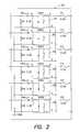
- FIG. 2is a schematic diagram of an interface board that is part of the system of FIG. 1;
- FIG. 3is a flow chart that illustrates valve control operations for an ALD process.
- FIG. 1is a schematic block diagram of the valve control system.
- reference numeral 10generally refers to the valve control system.
- the valve control system 10is for controlling a plurality of electrically-controlled valves 12 installed in association with a processing chamber 14 .
- the processing chamber 14may be a conventional chemical vapor deposition chamber, modified to optimize the throughput for ALD processing.
- the modifications to the processing chamber 14may include installing the valves 12 directly on the lid of the processing chamber 14 , and providing a process position for the substrate (not shown) that is very close to the gas distribution fixture (not shown) in the processing chamber 14 . Both of these modifications are designed to minimize the gas exposure cycle time.
- the valves 12are electronically-controlled valves, and are preferably type NC valves available from Fujikin of America Inc., Santa Clara, Calif. Each valve 12 is connected to a respective gas source 16 .
- the gas sources 16may include two or more process gas sources and a purge gas source.
- the valve control system 10includes a system control computer 18 and a programmable logic controller (PLC) 20 that is in data communication with the system control computer 18 via a communication channel 22 .
- the system control computer 18 and the PLC 20are programmed to operate in accordance with a master-slave arrangement such that the system control computer 18 delegates to the PLC 20 control of the valves 12 . More particularly, the system control computer 18 may download to the PLC 20 data that defines a valve operation recipe, and the PLC 20 then controls the valves 12 to carry out the downloaded valve control recipe.
- the system control computer 18may be a conventional personal computer programmed to control operation of the processing chamber 14 . Aside from the process and purge gas valve control functions delegated to the PLC 20 , the system control computer 18 may control all other functions of the processing chamber 14 , including control of, e.g., heaters, lifts, pumps, and valves such as exhaust valves that are different from the valves 12 controlled through the PLC 20 .
- a conventional control panel 24adapted to receive operator input, is connected to the system control computer 18 .
- the PLC 20is connected to the valves 12 via an interface board 26 and drivers 28 .
- the drivers 28may be constituted by circuitry sold by Fujikin under model number 23-6C-DR.
- the layout of interface board 26is schematically illustrated in FIG. 2 .
- FIG. 2is self-explanatory, but it will be noted that each signal channel of the board 26 includes a respective solid state relay 30 .
- the interface board 26serves to isolate the output of the PLC 20 from the drivers 28 .
- PLC 20may be constituted by a conventional device such as the Allen Bradley-MicroLogix model 1500.
- the PLC 20includes an output power supply 32 which provides power for signals outputted by the PLC 20 via field effect transistors (FETs) which are not shown.
- An interlock circuit 34is coupled to the power supply 32 of the PLC 20 .
- the interlock circuit 34is adapted to receive sensor signals to indicate conditions for which immediate shutdown of the process operation is required. Such conditions may be referred to as “interlock conditions” such as opening of the gas cabinet door (not shown).
- the interlock circuit 34upon the interlock circuit 34 receiving a signal indicative of an interlock condition, the interlock circuit 34 disables the power supply 32 of PLC 20 , thereby causing immediate closure of any open valve 12 .
- the system control computer 18is also coupled to the power supply 32 of PLC 20 for the purpose of disabling the power supply 32 and thereby shutting any open valve 12 upon receipt of a shutdown signal received from a human operator via control panel 24 .
- the system control computer 18may download commands to the PLC 20 , including a recipe for valve operation during an ALD process, via the communications channel 22 .
- the PLC 20may send data messages to the system control computer 18 via the communication channel 22 .
- Such data messagesmay include acknowledgement messages and status messages that indicate, for example, a number of gas exposure cycles that have been performed from a recipe in process, or that indicate that a recipe has been completed.
- the system control computer 18controls components of the processing chamber 14 to carry out functions such as loading a wafer for processing in the chamber 14 , positioning the wafer at an appropriate place in the chamber 14 for processing, and pumping out the chamber 14 .
- the system control computer 18downloads to the PLC 20 data that indicates the process recipe in terms of control of the valves 12 .
- the PLC 20outputs command signals to the valves 12 by way of interface board 26 and drivers 28 , to selectively open and close the valves 12 , and thereby to selectively expose the wafer in the processing chamber 14 to gases from gas sources 16 .
- FIG. 3is a flow chart that illustrates a sequence of functions initiated by the PLC 20 in connection with an ALD process performed in the processing chamber 14 .
- step 50Initially in the process of FIG. 3 is a step 50 , at which the PLC 20 increments a counter, which may have been reset in an initialization procedure (not shown).
- step 52at which the PLC 20 generates and outputs a command to open a first one of the valves 12 .
- the first one of the valves 12is connected to a source of a first process gas, which may be, for example, silane (SiH 4 ) or diborane (B 2 H 2 ).
- the first valvethen opens in response to the command from the PLC 20 and the first process gas enters the first processing chamber 14 and impinges on the wafer to deposit a first thin film on the wafer.
- the first valveis maintained in an open condition for a predetermined period of time which may be, for example, tens of milliseconds. Then, with a predetermined timing according to the recipe, the PLC 20 generates and transmits a command to close the first valve (step 54 ). The first valve is closed in response to the closing command. Simultaneously, the PLC 20 issues a command to open a second valve (step 56 ) which may be connected to a source of purge gas such as argon. Purge gas then flows into the chamber 14 .
- a source of purge gassuch as argon
- Purgingcontinues for a predetermined period of time, which may be on the order of a few hundred milliseconds, and then, with a predetermined timing, the PLC 20 issues a command (step 58 ) to close the second valve, thereby ending the purging.
- step 60the PLC 20 generates and transmits a command to open a third one of the valves 12 .
- the third valveis connected to a second source of process gas, which may be, for example, tungsten fluoride (WF 6 ).
- WF 6tungsten fluoride
- the second process gasUpon the opening of the third valve, the second process gas enters the chamber 14 and impinges on the wafer to deposit a second thin film layer on the wafer.
- the third valvemay be maintained in an open position for a predetermined period of time which may be tens of milliseconds.
- the PLC 20issues a command to close the third valve ( 62 ) and simultaneously issues a command to open the second valve (step 64 ) to initiate another purge.
- the purgingcontinues for a predetermined period of time, which may be the same as the purge of step 56 , and the purge is then terminated upon the PLC 20 issuing a command (step 66 ) to close the second valve.
- a brief stage in which a thin film is deposited on the wafer using a first process gasis followed by a purge stage, and then followed by a second brief stage in which a thin film is deposited on the wafer using a second process gas, followed by a second purge.
- These four stagesmay be considered to make up one cycle, and entail four commands to open valves and four commands to close valves.
- the control system 10is arranged, and the valves 12 are selected, so that the refresh time required to generate, transmit and execute a valve opening or closing command takes less than ten milliseconds.
- generation and transmission of the commandmay take less than 1 millisecond and execution of the command by the valve may take about 3 milliseconds.
- valve operation signals for each valve opening and closinghad been generated by and transmitted from the system control computer 18 .
- Conventional practices in this regardmight require up to one second or more for generation and transmission of each valve control command.
- the fast refresh time provided by the present inventionis also supported by the selection of the valves 12 and the drivers 28 of the types referred to above and by the use of solid state relays in interface board 26 .
- step 66is a decision block 68 at which it is determined whether the recipe for the ALD process has been completed. If not (i.e., if further cycles are required), the procedure of FIG. 3 loops back from decision block 68 to step 50 so that the counter is incremented and the cycle of steps 52 - 66 is performed again.
- a typical recipe for an ALD processmay call for as few as 10 to 20 cycles or as many as 200-300 cycles or more.
- a positive determinationis made at step 68 and the ALD process is completed (step 70 ). This may involve, for example, removing the wafer from the processing chamber 14 .
- the refresh cycle for process and purge gas valve opening and closing commandsis quite short with the arrangement of the present invention, the numerous valve operation cycles required for ALD can be performed rapidly, thereby enhancing throughput for the ALD process.
- the control system of the present inventionmay be arranged so that a hardware interlock is provided via the output power supply of the PLC 20 ; consequently safety regulations requiring hardware interlocks are complied with.
- the signal path from the PLC 20 to the valves 12may be implemented with high-speed and long-life solid state relays, so that a short refresh time is achieved, and the control system is durable notwithstanding the very numerous repetitive operations required of the relays.
- valves selected for the system of the present inventionrespond very rapidly to operational command signals so that the refresh time is minimized.
- valve control arrangement of the present inventionalso has the advantage of reducing the processing burden on the system control computer, since the large number of repetitive commands required for ALD processing are generated by the PLC 20 rather than the system control computer 18 .
- cyclic operating mode described in connection with FIG. 3is advantageous for ALD operations, it is also contemplated to operate the control system 10 in a non-cyclic operating mode, in which commands for directly opening or closing valves 12 may be generated by the system control computer 18 and transmitted one by one via the PLC 20 , the interface board 26 and the drivers 28 .
Landscapes
- Engineering & Computer Science (AREA)
- Physics & Mathematics (AREA)
- General Physics & Mathematics (AREA)
- Automation & Control Theory (AREA)
- Condensed Matter Physics & Semiconductors (AREA)
- Manufacturing & Machinery (AREA)
- Computer Hardware Design (AREA)
- Microelectronics & Electronic Packaging (AREA)
- Power Engineering (AREA)
- Chemical Vapour Deposition (AREA)
Abstract
Description
This invention is concerned with semiconductor manufacturing processes, and is more particularly concerned with apparatus and methods for controlling deposition chambers.
Semiconductor devices are made on substrates, such as silicon wafers or glass plates, for use in computers, monitors, and the like. These devices are made by a sequence of fabrication steps, such as thin film deposition, oxidation or nitration, etching, polishing, and thermal and lithographic processing.
Thin film deposition typically is performed in a low-pressure processing chamber. In chemical vapor deposition, a wafer or other substrate is loaded into a processing chamber and is exposed to a process gas under suitable conditions for deposition of the process gas or a component of the process gas in the form of a thin film on the wafer.
There are a number of different varieties of chemical vapor deposition processes, of which one of the more recently developed is referred to as atomic layer deposition (ALD) or atomic layer chemical vapor deposition (ALCVD). In atomic layer deposition, many thin film layers are deposited on the wafer in a repetitive process in which the wafer is alternately exposed to more than one process gas. Each cycle of an ALD process entails opening and closing a number of valves which control the flow to the processing chamber of process gases or a purge gas. Because each cycle is repeated numerous times, the amount of time required to generate, transmit and execute valve opening and closing commands may be a significant factor in the overall elapsed time required to complete an ALD process. The present inventors have recognized that a key to improving throughput for ALD processes lies in shortening the “refresh time” for valve control commands, where “refresh time” refers to the time required to generate, transmit and execute a command.
In accordance with the invention, there is provided a valve control system for a semiconductor processing chamber. The valve control system includes a system control computer and a plurality of electrically controlled valves associated with a processing chamber. The valve control system further includes a programmable logic controller in communication with the system control computer and operatively coupled to the electrically controlled valves. The programmable logic controller may control the electrically controlled valves with a refresh time of less than ten milliseconds, and preferably with a refresh time on the order of one millisecond (msec).
The valve control system may further include an interface board and a driver circuit coupling the programmable logic controller to the electrically controlled valves. The interface board may include solid state relays.
The programmable logic controller may include an output power supply adapted to provide an output signal from the programmable logic controller. The valve control system may further include an interlock circuit operatively coupled to the output power supply and adapted to disable the output power supply upon occurrence of an interlock condition.
The system control computer may be operatively coupled to the output power supply of the programmable logic controller and may be adapted to disable the output power supply in response to an operator input signal. The valve control system may include a control panel operatively connected to the system control computer and adapted to receive input from a human operator.
The plurality of electrically controlled valves of the valve control system may include a first valve, a second valve and a third valve. The first valve may be coupled to a source of a first process gas, the second valve may be coupled to a source of a second process gas, and the third valve may be coupled to a source of a purge gas.
According to another aspect of the invention, a method of operating a valve associated with a semiconductor processing chamber is provided. The method includes generating an operation command for the valve, transmitting the generated operation command to the valve, and executing the transmitted operation command at the valve. The generating, transmitting and executing steps may all be performed within a time period that does not exceed 10 msec.
According to still another aspect of the invention, a method of operating a valve associated with a semiconductor processing chamber is provided. The method includes providing an electrically-controlled valve and downloading a process recipe command from a system control computer to a programmable logic controller. The method further includes repeatedly generating open and close commands at the programmable logic controller in accordance with the downloaded process recipe command. Further included in the method are steps of transmitting the open and close commands from the programmable logic controller to the electrically-controlled valve, and repeatedly opening and closing the electrically-controlled valve in response to the transmitted open and close commands.
The method according to this aspect of the invention may further include flowing a process gas or a purge gas to the semiconductor processing chamber in response to the opening of the electrically-controlled valve.
With the valve control system arranged in accordance with the invention, commands to open or close valves for process gases or purge gas may be generated and executed with a refresh time on the order of one millisecond. With such a rapid refresh time, the many repetitive gas flow cycles required for ALD can be performed in an efficient manner, thereby increasing throughput.
Aspects of the invention also call for a hardware interlock operating through the output power supply of the programmable logic controller so that safety requirements are satisfied. Moreover, in accordance with an aspect of the invention, solid state relays are employed in interface circuitry which interconnects the PLC with the valves. The use of solid state relays allows the system to operate with a long life, notwithstanding the very numerous open-close cycles required for ALD processing.
Further features and advantages of the present invention will become more fully apparent from the following detailed description of a preferred embodiment, the appended claims and the accompanying drawings.
FIG. 1 is a schematic block diagram of a valve control system provided in accordance with an embodiment of the invention;
FIG. 2 is a schematic diagram of an interface board that is part of the system of FIG. 1; and
FIG. 3 is a flow chart that illustrates valve control operations for an ALD process.
A valve control system provided in accordance with an embodiment of the invention will now be described with reference to FIG. 1, which is a schematic block diagram of the valve control system. In FIG. 1reference numeral 10 generally refers to the valve control system. Thevalve control system 10 is for controlling a plurality of electrically-controlledvalves 12 installed in association with aprocessing chamber 14. Theprocessing chamber 14 may be a conventional chemical vapor deposition chamber, modified to optimize the throughput for ALD processing. The modifications to theprocessing chamber 14 may include installing thevalves 12 directly on the lid of theprocessing chamber 14, and providing a process position for the substrate (not shown) that is very close to the gas distribution fixture (not shown) in theprocessing chamber 14. Both of these modifications are designed to minimize the gas exposure cycle time.
Thevalves 12, as noted before, are electronically-controlled valves, and are preferably type NC valves available from Fujikin of America Inc., Santa Clara, Calif. Eachvalve 12 is connected to arespective gas source 16. Thegas sources 16 may include two or more process gas sources and a purge gas source.
Thevalve control system 10 includes asystem control computer 18 and a programmable logic controller (PLC)20 that is in data communication with thesystem control computer 18 via acommunication channel 22. Thesystem control computer 18 and thePLC 20 are programmed to operate in accordance with a master-slave arrangement such that thesystem control computer 18 delegates to thePLC 20 control of thevalves 12. More particularly, thesystem control computer 18 may download to thePLC 20 data that defines a valve operation recipe, and thePLC 20 then controls thevalves 12 to carry out the downloaded valve control recipe.
Thesystem control computer 18 may be a conventional personal computer programmed to control operation of theprocessing chamber 14. Aside from the process and purge gas valve control functions delegated to thePLC 20, thesystem control computer 18 may control all other functions of theprocessing chamber 14, including control of, e.g., heaters, lifts, pumps, and valves such as exhaust valves that are different from thevalves 12 controlled through thePLC 20. Aconventional control panel 24, adapted to receive operator input, is connected to thesystem control computer 18.
ThePLC 20 is connected to thevalves 12 via aninterface board 26 anddrivers 28. Thedrivers 28 may be constituted by circuitry sold by Fujikin under model number 23-6C-DR. The layout ofinterface board 26 is schematically illustrated in FIG.2. FIG. 2 is self-explanatory, but it will be noted that each signal channel of theboard 26 includes a respectivesolid state relay 30. Theinterface board 26 serves to isolate the output of thePLC 20 from thedrivers 28.
Continuing to refer to FIG. 1, PLC20 may be constituted by a conventional device such as the Allen Bradley-MicroLogix model 1500. ThePLC 20 includes anoutput power supply 32 which provides power for signals outputted by thePLC 20 via field effect transistors (FETs) which are not shown. Aninterlock circuit 34 is coupled to thepower supply 32 of thePLC 20. In accordance with conventional practice, theinterlock circuit 34 is adapted to receive sensor signals to indicate conditions for which immediate shutdown of the process operation is required. Such conditions may be referred to as “interlock conditions” such as opening of the gas cabinet door (not shown). In accordance with the invention, upon theinterlock circuit 34 receiving a signal indicative of an interlock condition, theinterlock circuit 34 disables thepower supply 32 ofPLC 20, thereby causing immediate closure of anyopen valve 12.
Thesystem control computer 18 is also coupled to thepower supply 32 ofPLC 20 for the purpose of disabling thepower supply 32 and thereby shutting anyopen valve 12 upon receipt of a shutdown signal received from a human operator viacontrol panel 24.
Thesystem control computer 18 may download commands to thePLC 20, including a recipe for valve operation during an ALD process, via thecommunications channel 22. Moreover, thePLC 20 may send data messages to thesystem control computer 18 via thecommunication channel 22. Such data messages may include acknowledgement messages and status messages that indicate, for example, a number of gas exposure cycles that have been performed from a recipe in process, or that indicate that a recipe has been completed.
In operation, thesystem control computer 18 controls components of theprocessing chamber 14 to carry out functions such as loading a wafer for processing in thechamber 14, positioning the wafer at an appropriate place in thechamber 14 for processing, and pumping out thechamber 14. At a time when thechamber 14 is ready to perform an atomic layer deposition process, thesystem control computer 18 downloads to thePLC 20 data that indicates the process recipe in terms of control of thevalves 12. On the basis of the downloaded data, thePLC 20 outputs command signals to thevalves 12 by way ofinterface board 26 anddrivers 28, to selectively open and close thevalves 12, and thereby to selectively expose the wafer in theprocessing chamber 14 to gases fromgas sources 16.
FIG. 3 is a flow chart that illustrates a sequence of functions initiated by thePLC 20 in connection with an ALD process performed in theprocessing chamber 14.
Initially in the process of FIG. 3 is astep 50, at which thePLC 20 increments a counter, which may have been reset in an initialization procedure (not shown). Followingstep 50 isstep 52, at which thePLC 20 generates and outputs a command to open a first one of thevalves 12. It is assumed that the first one of thevalves 12 is connected to a source of a first process gas, which may be, for example, silane (SiH4) or diborane (B2H2). The first valve then opens in response to the command from thePLC 20 and the first process gas enters thefirst processing chamber 14 and impinges on the wafer to deposit a first thin film on the wafer. The first valve is maintained in an open condition for a predetermined period of time which may be, for example, tens of milliseconds. Then, with a predetermined timing according to the recipe, thePLC 20 generates and transmits a command to close the first valve (step54). The first valve is closed in response to the closing command. Simultaneously, thePLC 20 issues a command to open a second valve (step56) which may be connected to a source of purge gas such as argon. Purge gas then flows into thechamber 14. Purging continues for a predetermined period of time, which may be on the order of a few hundred milliseconds, and then, with a predetermined timing, thePLC 20 issues a command (step58) to close the second valve, thereby ending the purging.
Followingstep 58 isstep 60. Atstep 60 thePLC 20 generates and transmits a command to open a third one of thevalves 12. It is assumed that the third valve is connected to a second source of process gas, which may be, for example, tungsten fluoride (WF6). Upon the opening of the third valve, the second process gas enters thechamber 14 and impinges on the wafer to deposit a second thin film layer on the wafer. The third valve may be maintained in an open position for a predetermined period of time which may be tens of milliseconds. Then, at a predetermined timing, thePLC 20 issues a command to close the third valve (62) and simultaneously issues a command to open the second valve (step64) to initiate another purge. The purging continues for a predetermined period of time, which may be the same as the purge ofstep 56, and the purge is then terminated upon thePLC 20 issuing a command (step66) to close the second valve.
To summarize what has occurred in steps52-66, a brief stage in which a thin film is deposited on the wafer using a first process gas is followed by a purge stage, and then followed by a second brief stage in which a thin film is deposited on the wafer using a second process gas, followed by a second purge. These four stages may be considered to make up one cycle, and entail four commands to open valves and four commands to close valves. In one aspect, thecontrol system 10 is arranged, and thevalves 12 are selected, so that the refresh time required to generate, transmit and execute a valve opening or closing command takes less than ten milliseconds. For example, generation and transmission of the command may take less than 1 millisecond and execution of the command by the valve may take about 3 milliseconds. Such would not have been the case if, in accordance with conventional practices, valve operation signals for each valve opening and closing had been generated by and transmitted from thesystem control computer 18. Conventional practices in this regard might require up to one second or more for generation and transmission of each valve control command. The fast refresh time provided by the present invention is also supported by the selection of thevalves 12 and thedrivers 28 of the types referred to above and by the use of solid state relays ininterface board 26.
Followingstep 66 is adecision block 68 at which it is determined whether the recipe for the ALD process has been completed. If not (i.e., if further cycles are required), the procedure of FIG. 3 loops back fromdecision block 68 to step50 so that the counter is incremented and the cycle of steps52-66 is performed again. A typical recipe for an ALD process may call for as few as 10 to 20 cycles or as many as 200-300 cycles or more. Once the number of cycles called for by the recipe has been performed, a positive determination is made atstep 68 and the ALD process is completed (step70). This may involve, for example, removing the wafer from theprocessing chamber 14.
Because the refresh cycle for process and purge gas valve opening and closing commands is quite short with the arrangement of the present invention, the numerous valve operation cycles required for ALD can be performed rapidly, thereby enhancing throughput for the ALD process. Furthermore, the control system of the present invention may be arranged so that a hardware interlock is provided via the output power supply of thePLC 20; consequently safety regulations requiring hardware interlocks are complied with. Still further, the signal path from thePLC 20 to thevalves 12 may be implemented with high-speed and long-life solid state relays, so that a short refresh time is achieved, and the control system is durable notwithstanding the very numerous repetitive operations required of the relays.
Moreover, the valves selected for the system of the present invention respond very rapidly to operational command signals so that the refresh time is minimized.
The valve control arrangement of the present invention also has the advantage of reducing the processing burden on the system control computer, since the large number of repetitive commands required for ALD processing are generated by thePLC 20 rather than thesystem control computer 18.
Although the cyclic operating mode described in connection with FIG. 3 is advantageous for ALD operations, it is also contemplated to operate thecontrol system 10 in a non-cyclic operating mode, in which commands for directly opening or closingvalves 12 may be generated by thesystem control computer 18 and transmitted one by one via thePLC 20, theinterface board 26 and thedrivers 28.
The foregoing description discloses only a preferred embodiment of the invention; modifications of the above disclosed apparatus which fall within the scope of the invention will be readily apparent to those of ordinary skill in the art. Accordingly, while the present invention has been disclosed in connection with a preferred embodiment thereof, it should be understood that other embodiments may fall within the spirit and scope of the invention, as defined by the following claims.
Claims (11)
1. A valve control system for a semiconductor processing chamber, comprising:
a system control computer;
a plurality of electrically controlled valves associated with a processing chamber; and
a programmable logic controller in communication with the system control computer and operatively coupled to the electrically controlled valves, wherein the programmable logic controller controls the electrically controlled valves with a refresh time of less than 10 msec.
2. The valve control system ofclaim 1 , further comprising an interface board and a driver circuit coupling the programmable logic controller to the electrically controlled valves.
3. The valve control system ofclaim 2 , wherein the interface board includes solid state relays.
4. The valve control system ofclaim 1 , wherein the programmable logic controller includes an output power supply adapted to provide an output signal from the programmable logic controller; and further comprising an interlock circuit operatively coupled to the output power supply and adapted to disable the output power supply upon occurrence of an interlock condition.
5. The valve control system ofclaim 4 , wherein the system control computer is operatively coupled to the output power supply and is adapted to disable the output power supply in response to an operator input signal.
6. The valve control system ofclaim 5 , further comprising a control panel operatively connected to the system control computer and adapted to receive input from a human operator.
7. The valve control system ofclaim 1 , wherein the plurality of electrically controlled valves includes a first valve, a second valve and a third valve, and wherein:
the first valve is coupled to a source of a first process gas;
the second valve is coupled to a source of a second process gas; and
the third valve is coupled to a source of a purge gas.
8. A valve control system for a semiconductor processing chamber, comprising:
a system control computer;
a plurality of electrically controlled valves associated with a processing chamber; and
a programmable logic controller in communication with the system control computer and operatively coupled to the electrically controlled valves, wherein the programmable logic controller includes an output power supply adapted to provide an output signal from the programmable logic controller; and further comprising an interlock circuit operatively coupled to the output power supply and adapted to disable the output power supply upon occurrence of an interlock condition.
9. The valve control system ofclaim 8 , wherein the system control computer is operatively coupled to the output power supply and is adapted to disable the output power supply in response to an operator input signal.
10. The valve control system ofclaim 9 , further comprising a control panel operatively connected to the system control computer and adapted to receive input from a human operator.
11. The valve control system ofclaim 8 , wherein the plurality of electrically controlled valves includes a first valve, a second valve and a third valve, and wherein:
the first valve is coupled to a source of a first process gas;
the second valve is coupled to a source of a second process gas; and
the third valve is coupled to a source of a purge gas.
Priority Applications (8)
| Application Number | Priority Date | Filing Date | Title |
|---|---|---|---|
| US09/800,881US6734020B2 (en) | 2001-03-07 | 2001-03-07 | Valve control system for atomic layer deposition chamber |
| CNA028086600ACN1529839A (en) | 2001-03-07 | 2002-03-06 | Valve Control System of Atomic Layer Deposition Chamber |
| AU2002255664AAU2002255664A1 (en) | 2001-03-07 | 2002-03-06 | Valve control system for atomic layer deposition chamber |
| PCT/US2002/006778WO2002073329A2 (en) | 2001-03-07 | 2002-03-06 | Valve control system for atomic layer deposition chamber |
| KR1020020011896AKR20020071765A (en) | 2001-03-07 | 2002-03-06 | Valve control system for atomic layer deposition chamber |
| TW091104325ATW569310B (en) | 2001-03-07 | 2002-03-07 | Valve control system for atomic layer deposition chamber |
| JP2002109810AJP2002329674A (en) | 2001-03-07 | 2002-03-07 | Valve control system for semiconductor processing chamber |
| US10/731,651US7201803B2 (en) | 2001-03-07 | 2003-12-09 | Valve control system for atomic layer deposition chamber |
Applications Claiming Priority (1)
| Application Number | Priority Date | Filing Date | Title |
|---|---|---|---|
| US09/800,881US6734020B2 (en) | 2001-03-07 | 2001-03-07 | Valve control system for atomic layer deposition chamber |
Related Child Applications (1)
| Application Number | Title | Priority Date | Filing Date |
|---|---|---|---|
| US10/731,651DivisionUS7201803B2 (en) | 2001-03-07 | 2003-12-09 | Valve control system for atomic layer deposition chamber |
Publications (2)
| Publication Number | Publication Date |
|---|---|
| US20020127745A1 US20020127745A1 (en) | 2002-09-12 |
| US6734020B2true US6734020B2 (en) | 2004-05-11 |
Family
ID=25179620
Family Applications (2)
| Application Number | Title | Priority Date | Filing Date |
|---|---|---|---|
| US09/800,881Expired - LifetimeUS6734020B2 (en) | 2001-03-07 | 2001-03-07 | Valve control system for atomic layer deposition chamber |
| US10/731,651Expired - LifetimeUS7201803B2 (en) | 2001-03-07 | 2003-12-09 | Valve control system for atomic layer deposition chamber |
Family Applications After (1)
| Application Number | Title | Priority Date | Filing Date |
|---|---|---|---|
| US10/731,651Expired - LifetimeUS7201803B2 (en) | 2001-03-07 | 2003-12-09 | Valve control system for atomic layer deposition chamber |
Country Status (7)
| Country | Link |
|---|---|
| US (2) | US6734020B2 (en) |
| JP (1) | JP2002329674A (en) |
| KR (1) | KR20020071765A (en) |
| CN (1) | CN1529839A (en) |
| AU (1) | AU2002255664A1 (en) |
| TW (1) | TW569310B (en) |
| WO (1) | WO2002073329A2 (en) |
Cited By (68)
| Publication number | Priority date | Publication date | Assignee | Title |
|---|---|---|---|---|
| US20030023338A1 (en)* | 2001-07-27 | 2003-01-30 | Applied Materials, Inc. | Atomic layer deposition apparatus |
| US20030121608A1 (en)* | 2001-10-26 | 2003-07-03 | Applied Materials, Inc. | Gas delivery apparatus for atomic layer deposition |
| US20030172872A1 (en)* | 2002-01-25 | 2003-09-18 | Applied Materials, Inc. | Apparatus for cyclical deposition of thin films |
| US20030172873A1 (en)* | 2002-03-15 | 2003-09-18 | Diego Fischer | Apparatus and method for the production of flexible semiconductor devices |
| US20030211015A1 (en)* | 2002-05-08 | 2003-11-13 | Taiwan Semiconductor Manufacturing Co., Ltd. | Gas flow control system with interlock |
| US20030224600A1 (en)* | 2002-03-04 | 2003-12-04 | Wei Cao | Sequential deposition of tantalum nitride using a tantalum-containing precursor and a nitrogen-containing precursor |
| US20040069227A1 (en)* | 2002-10-09 | 2004-04-15 | Applied Materials, Inc. | Processing chamber configured for uniform gas flow |
| US20040144311A1 (en)* | 2002-11-14 | 2004-07-29 | Ling Chen | Apparatus and method for hybrid chemical processing |
| US20040211665A1 (en)* | 2001-07-25 | 2004-10-28 | Yoon Ki Hwan | Barrier formation using novel sputter-deposition method |
| US20050045102A1 (en)* | 2003-08-28 | 2005-03-03 | Zheng Lingyi A. | Methods and apparatus for processing microfeature workpieces, e.g., for depositing materials on microfeature workpieces |
| US20050095859A1 (en)* | 2003-11-03 | 2005-05-05 | Applied Materials, Inc. | Precursor delivery system with rate control |
| US20050100669A1 (en)* | 2003-11-12 | 2005-05-12 | Veeco Instruments, Inc. | Method and apparatus for fabricating a conformal thin film on a substrate |
| US20050120954A1 (en)* | 2002-05-24 | 2005-06-09 | Carpenter Craig M. | Apparatus for controlling gas pulsing in processes for depositing materials onto micro-device workpieces |
| US20050139160A1 (en)* | 2002-01-26 | 2005-06-30 | Applied Materials, Inc. | Clamshell and small volume chamber with fixed substrate support |
| US20050189072A1 (en)* | 2002-07-17 | 2005-09-01 | Applied Materials, Inc. | Method and apparatus of generating PDMAT precursor |
| US20050209783A1 (en)* | 1996-12-20 | 2005-09-22 | Bittleston Simon H | Control devices for controlling the position of a marine seismic streamer |
| US20060021573A1 (en)* | 2004-06-28 | 2006-02-02 | Cambridge Nanotech Inc. | Vapor deposition systems and methods |
| US20060035025A1 (en)* | 2002-10-11 | 2006-02-16 | Applied Materials, Inc. | Activated species generator for rapid cycle deposition processes |
| US7037574B2 (en) | 2001-05-23 | 2006-05-02 | Veeco Instruments, Inc. | Atomic layer deposition for fabricating thin films |
| US20060216548A1 (en)* | 2005-03-22 | 2006-09-28 | Ming Mao | Nanolaminate thin films and method for forming the same using atomic layer deposition |
| US20060272577A1 (en)* | 2005-06-03 | 2006-12-07 | Ming Mao | Method and apparatus for decreasing deposition time of a thin film |
| US20070003698A1 (en)* | 2001-10-26 | 2007-01-04 | Ling Chen | Enhanced copper growth with ultrathin barrier layer for high performance interconnects |
| US20070048869A1 (en)* | 2005-08-24 | 2007-03-01 | Beung-Keun Lee | Valve system and deposition apparatus including valve system and atomic layer deposition chamber |
| US20070079759A1 (en)* | 2005-10-07 | 2007-04-12 | Applied Materials, Inc. | Ampoule splash guard apparatus |
| US20070173076A1 (en)* | 2006-01-24 | 2007-07-26 | Kyoung-Chon Kim | Equipment for sensing malfunctioning roughing valves in an ion implantation apparatus |
| US7258892B2 (en) | 2003-12-10 | 2007-08-21 | Micron Technology, Inc. | Methods and systems for controlling temperature during microfeature workpiece processing, e.g., CVD deposition |
| US7279398B2 (en) | 2003-09-17 | 2007-10-09 | Micron Technology, Inc. | Microfeature workpiece processing apparatus and methods for controlling deposition of materials on microfeature workpieces |
| US7294208B2 (en) | 2002-07-29 | 2007-11-13 | Applied Materials, Inc. | Apparatus for providing gas to a processing chamber |
| US7323231B2 (en) | 2003-10-09 | 2008-01-29 | Micron Technology, Inc. | Apparatus and methods for plasma vapor deposition processes |
| US7335396B2 (en) | 2003-04-24 | 2008-02-26 | Micron Technology, Inc. | Methods for controlling mass flow rates and pressures in passageways coupled to reaction chambers and systems for depositing material onto microfeature workpieces in reaction chambers |
| US7342984B1 (en) | 2003-04-03 | 2008-03-11 | Zilog, Inc. | Counting clock cycles over the duration of a first character and using a remainder value to determine when to sample a bit of a second character |
| US7344755B2 (en) | 2003-08-21 | 2008-03-18 | Micron Technology, Inc. | Methods and apparatus for processing microfeature workpieces; methods for conditioning ALD reaction chambers |
| US7352048B2 (en) | 2001-09-26 | 2008-04-01 | Applied Materials, Inc. | Integration of barrier layer and seed layer |
| US20080099933A1 (en)* | 2006-10-31 | 2008-05-01 | Choi Kenric T | Ampoule for liquid draw and vapor draw with a continous level sensor |
| US20080107809A1 (en)* | 2001-10-26 | 2008-05-08 | Dien-Yeh Wu | Vortex chamber lids for atomic layer deposition |
| US20080105901A1 (en)* | 2006-11-07 | 2008-05-08 | Kamal Tabatabaie | Atomic layer deposition in the formation of gate structures for iii-v semiconductor |
| US7387685B2 (en) | 2002-07-08 | 2008-06-17 | Micron Technology, Inc. | Apparatus and method for depositing materials onto microelectronic workpieces |
| US7402534B2 (en) | 2005-08-26 | 2008-07-22 | Applied Materials, Inc. | Pretreatment processes within a batch ALD reactor |
| US20080208366A1 (en)* | 2005-01-07 | 2008-08-28 | Norgen Limited | Communication System Comprising a Controller System and a Master Control Means Connected Via a Multipole Connection Means |
| US20080202425A1 (en)* | 2007-01-29 | 2008-08-28 | Applied Materials, Inc. | Temperature controlled lid assembly for tungsten nitride deposition |
| US20080268171A1 (en)* | 2005-11-04 | 2008-10-30 | Paul Ma | Apparatus and process for plasma-enhanced atomic layer deposition |
| US7547952B2 (en) | 2003-04-04 | 2009-06-16 | Applied Materials, Inc. | Method for hafnium nitride deposition |
| US7584942B2 (en) | 2004-03-31 | 2009-09-08 | Micron Technology, Inc. | Ampoules for producing a reaction gas and systems for depositing materials onto microfeature workpieces in reaction chambers |
| US7588804B2 (en) | 2002-08-15 | 2009-09-15 | Micron Technology, Inc. | Reactors with isolated gas connectors and methods for depositing materials onto micro-device workpieces |
| US7601648B2 (en) | 2006-07-31 | 2009-10-13 | Applied Materials, Inc. | Method for fabricating an integrated gate dielectric layer for field effect transistors |
| US7611990B2 (en) | 2001-07-25 | 2009-11-03 | Applied Materials, Inc. | Deposition methods for barrier and tungsten materials |
| US20100059059A1 (en)* | 2008-09-09 | 2010-03-11 | Perry Baromedical Corporation | Hyperbaric chamber |
| US7699932B2 (en) | 2004-06-02 | 2010-04-20 | Micron Technology, Inc. | Reactors, systems and methods for depositing thin films onto microfeature workpieces |
| US7781326B2 (en)* | 2001-02-02 | 2010-08-24 | Applied Materials, Inc. | Formation of a tantalum-nitride layer |
| US7794544B2 (en) | 2004-05-12 | 2010-09-14 | Applied Materials, Inc. | Control of gas flow and delivery to suppress the formation of particles in an MOCVD/ALD system |
| US7798096B2 (en) | 2006-05-05 | 2010-09-21 | Applied Materials, Inc. | Plasma, UV and ion/neutral assisted ALD or CVD in a batch tool |
| US20100266765A1 (en)* | 2009-04-21 | 2010-10-21 | White Carl L | Method and apparatus for growing a thin film onto a substrate |
| US7871470B2 (en) | 2003-03-12 | 2011-01-18 | Applied Materials, Inc. | Substrate support lift mechanism |
| US7905959B2 (en) | 2001-07-16 | 2011-03-15 | Applied Materials, Inc. | Lid assembly for a processing system to facilitate sequential deposition techniques |
| US20110200822A1 (en)* | 2008-10-20 | 2011-08-18 | Christophe Detavernier | Atomic layer deposition powder coating |
| US8110489B2 (en) | 2001-07-25 | 2012-02-07 | Applied Materials, Inc. | Process for forming cobalt-containing materials |
| US8119210B2 (en) | 2004-05-21 | 2012-02-21 | Applied Materials, Inc. | Formation of a silicon oxynitride layer on a high-k dielectric material |
| US8133554B2 (en) | 2004-05-06 | 2012-03-13 | Micron Technology, Inc. | Methods for depositing material onto microfeature workpieces in reaction chambers and systems for depositing materials onto microfeature workpieces |
| US8146896B2 (en) | 2008-10-31 | 2012-04-03 | Applied Materials, Inc. | Chemical precursor ampoule for vapor deposition processes |
| US8187970B2 (en) | 2001-07-25 | 2012-05-29 | Applied Materials, Inc. | Process for forming cobalt and cobalt silicide materials in tungsten contact applications |
| US8323754B2 (en) | 2004-05-21 | 2012-12-04 | Applied Materials, Inc. | Stabilization of high-k dielectric materials |
| US8384192B2 (en) | 2004-01-28 | 2013-02-26 | Micron Technology, Inc. | Methods for forming small-scale capacitor structures |
| TWI410518B (en)* | 2006-10-24 | 2013-10-01 | Applied Materials Inc | Vortex chamber lids for atomic layer deposition |
| US20150079310A1 (en)* | 2013-09-16 | 2015-03-19 | Daejin University Center For Educational Industrial Cooperation | In situ system and method of manufacturing nanoparticles having core-shell structure |
| US9051641B2 (en) | 2001-07-25 | 2015-06-09 | Applied Materials, Inc. | Cobalt deposition on barrier surfaces |
| US9856985B2 (en)* | 2013-03-15 | 2018-01-02 | Numatics, Incorporated | Valve manifold circuit board with serial communication circuit line |
| US20180023718A1 (en)* | 2013-03-15 | 2018-01-25 | Numatics, Incorporated | Valve manifold circuit board with serial communication and control circuit line |
| US10256075B2 (en) | 2016-01-22 | 2019-04-09 | Applied Materials, Inc. | Gas splitting by time average injection into different zones by fast gas valves |
Families Citing this family (29)
| Publication number | Priority date | Publication date | Assignee | Title |
|---|---|---|---|---|
| JP3741253B2 (en)* | 1999-12-24 | 2006-02-01 | 富士通株式会社 | Chemical manufacturing equipment |
| US6861094B2 (en)* | 2002-04-25 | 2005-03-01 | Micron Technology, Inc. | Methods for forming thin layers of materials on micro-device workpieces |
| KR100445298B1 (en)* | 2002-05-03 | 2004-08-21 | 씨앤에스엔지니어링 주식회사 | Interface board |
| US7118783B2 (en)* | 2002-06-26 | 2006-10-10 | Micron Technology, Inc. | Methods and apparatus for vapor processing of micro-device workpieces |
| US7244683B2 (en) | 2003-01-07 | 2007-07-17 | Applied Materials, Inc. | Integration of ALD/CVD barriers with porous low k materials |
| US7235138B2 (en) | 2003-08-21 | 2007-06-26 | Micron Technology, Inc. | Microfeature workpiece processing apparatus and methods for batch deposition of materials on microfeature workpieces |
| US7282239B2 (en) | 2003-09-18 | 2007-10-16 | Micron Technology, Inc. | Systems and methods for depositing material onto microfeature workpieces in reaction chambers |
| US7581511B2 (en) | 2003-10-10 | 2009-09-01 | Micron Technology, Inc. | Apparatus and methods for manufacturing microfeatures on workpieces using plasma vapor processes |
| US7647886B2 (en) | 2003-10-15 | 2010-01-19 | Micron Technology, Inc. | Systems for depositing material onto workpieces in reaction chambers and methods for removing byproducts from reaction chambers |
| JP4933809B2 (en)* | 2006-03-13 | 2012-05-16 | 株式会社日立国際電気 | Substrate processing apparatus, substrate processing method, and substrate processing apparatus determination program |
| JP2011159279A (en)* | 2010-01-07 | 2011-08-18 | Canon Anelva Corp | Vacuum processing device, and method of processing parameter in plc |
| US9284643B2 (en)* | 2010-03-23 | 2016-03-15 | Pneumaticoat Technologies Llc | Semi-continuous vapor deposition process for the manufacture of coated particles |
| US8997686B2 (en) | 2010-09-29 | 2015-04-07 | Mks Instruments, Inc. | System for and method of fast pulse gas delivery |
| US9348339B2 (en)* | 2010-09-29 | 2016-05-24 | Mks Instruments, Inc. | Method and apparatus for multiple-channel pulse gas delivery system |
| US10126760B2 (en) | 2011-02-25 | 2018-11-13 | Mks Instruments, Inc. | System for and method of fast pulse gas delivery |
| US10031531B2 (en) | 2011-02-25 | 2018-07-24 | Mks Instruments, Inc. | System for and method of multiple channel fast pulse gas delivery |
| US10353408B2 (en) | 2011-02-25 | 2019-07-16 | Mks Instruments, Inc. | System for and method of fast pulse gas delivery |
| JP6022908B2 (en) | 2012-01-16 | 2016-11-09 | 東京エレクトロン株式会社 | Processing apparatus and valve operation confirmation method |
| JP5824372B2 (en)* | 2012-01-25 | 2015-11-25 | 東京エレクトロン株式会社 | Processing apparatus and process status confirmation method |
| US8936831B2 (en) | 2012-02-03 | 2015-01-20 | Uchicago Argonne, Llc | Method for fluidizing and coating ultrafine particles, device for fluidizing and coating ultrafine particles |
| US20130237063A1 (en)* | 2012-03-09 | 2013-09-12 | Seshasayee Varadarajan | Split pumping method, apparatus, and system |
| JP6697706B2 (en)* | 2015-12-07 | 2020-05-27 | 凸版印刷株式会社 | Atomic layer deposition equipment |
| US20200379445A1 (en) | 2017-12-12 | 2020-12-03 | Telefonaktiebolaget Lm Ericsson (Publ) | Improved Latency Management |
| CN111101115B (en)* | 2018-10-25 | 2022-03-22 | 北京北方华创微电子装备有限公司 | Gas path switching device, control method thereof and semiconductor processing equipment |
| JP7454915B2 (en) | 2019-04-11 | 2024-03-25 | 東京エレクトロン株式会社 | Processing equipment and processing method |
| JP6789354B1 (en)* | 2019-06-25 | 2020-11-25 | 株式会社アルバック | Surface treatment method |
| US11586573B2 (en)* | 2020-11-18 | 2023-02-21 | Applied Materials, Inc. | Distributed input/output (IO) control and interlock ring architecture |
| US20230369083A1 (en)* | 2022-05-10 | 2023-11-16 | University Of Washington | Method for operating reactor system |
| CN115562107A (en)* | 2022-09-27 | 2023-01-03 | 上海陛通半导体能源科技股份有限公司 | Valve control system based on Ether CAT extreme speed control technology |
Citations (203)
| Publication number | Priority date | Publication date | Assignee | Title |
|---|---|---|---|---|
| US4058430A (en) | 1974-11-29 | 1977-11-15 | Tuomo Suntola | Method for producing compound thin films |
| US4263091A (en) | 1980-01-25 | 1981-04-21 | Phillips Petroleum Company | Fluid flow control |
| US4389973A (en) | 1980-03-18 | 1983-06-28 | Oy Lohja Ab | Apparatus for performing growth of compound thin films |
| US4413022A (en) | 1979-02-28 | 1983-11-01 | Canon Kabushiki Kaisha | Method for performing growth of compound thin films |
| US4486487A (en) | 1982-05-10 | 1984-12-04 | Oy Lohja Ab | Combination film, in particular for thin film electroluminescent structures |
| JPS6065712A (en) | 1983-09-20 | 1985-04-15 | Toshiba Corp | Method of forming silicon oxide film |
| US4542044A (en)* | 1983-11-17 | 1985-09-17 | Owens-Corning Fiberglas Corporation | Method and apparatus to automatically apply a liquid dust inhibitor to fiberglass blowing wool |
| US4571319A (en) | 1984-04-05 | 1986-02-18 | General Motors Corporation | Method and apparatus for producing polymer articles having different properties in different regions of the articles |
| JPS6291495A (en) | 1985-10-15 | 1987-04-25 | Nec Corp | Vapor growth method for thin semiconductor film |
| US4767494A (en) | 1986-07-04 | 1988-08-30 | Nippon Telegraph & Telephone Corporation | Preparation process of compound semiconductor |
| US4806321A (en) | 1984-07-26 | 1989-02-21 | Research Development Corporation Of Japan | Use of infrared radiation and an ellipsoidal reflection mirror |
| US4813846A (en) | 1987-02-13 | 1989-03-21 | Leybold-Heraeus Gmbh | Inserting device for vacuum apparatus |
| US4829022A (en) | 1985-12-09 | 1989-05-09 | Nippon Telegraph And Telephone Corporation | Method for forming thin films of compound semiconductors by flow rate modulation epitaxy |
| US4834831A (en) | 1986-09-08 | 1989-05-30 | Research Development Corporation Of Japan | Method for growing single crystal thin films of element semiconductor |
| US4835701A (en) | 1986-04-23 | 1989-05-30 | Kawasaki Steel Corp. | Post-mix method and system for supply of powderized materials |
| US4838983A (en) | 1986-07-03 | 1989-06-13 | Emcore, Inc. | Gas treatment apparatus and method |
| US4838993A (en) | 1986-12-04 | 1989-06-13 | Seiko Instruments Inc. | Method of fabricating MOS field effect transistor |
| US4840921A (en) | 1987-07-01 | 1989-06-20 | Nec Corporation | Process for the growth of III-V group compound semiconductor crystal on a Si substrate |
| US4845049A (en) | 1987-03-27 | 1989-07-04 | Nec Corporation | Doping III-V compound semiconductor devices with group VI monolayers using ALE |
| FR2626110A1 (en) | 1988-01-19 | 1989-07-21 | Thomson Csf | Process for producing a layer of a superconductive material by epitaxy |
| US4859627A (en) | 1987-07-01 | 1989-08-22 | Nec Corporation | Group VI doping of III-V semiconductors during ALE |
| US4859625A (en) | 1986-11-22 | 1989-08-22 | Research Development Corporation of Japan, Junichi Nishizawa and Oki Electric Industry Co., Ltd. | Method for epitaxial growth of compound semiconductor using MOCVD with molecular layer epitaxy |
| US4861417A (en) | 1987-03-27 | 1989-08-29 | Fujitsu Limited | Method of growing group III-V compound semiconductor epitaxial layer |
| US4876218A (en) | 1987-09-29 | 1989-10-24 | Oy Nokia Ab | Method of growing GaAs films on Si or GaAs substrates using ale |
| EP0344352A1 (en) | 1988-06-03 | 1989-12-06 | International Business Machines Corporation | Method for making artificial layered high-Tc superconductors |
| US4917556A (en) | 1986-04-28 | 1990-04-17 | Varian Associates, Inc. | Modular wafer transport and processing system |
| US4927670A (en) | 1988-06-22 | 1990-05-22 | Georgia Tech Research Corporation | Chemical vapor deposition of mixed metal oxide coatings |
| US4931132A (en) | 1988-10-07 | 1990-06-05 | Bell Communications Research, Inc. | Optical control of deposition of crystal monolayers |
| US4951601A (en) | 1986-12-19 | 1990-08-28 | Applied Materials, Inc. | Multi-chamber integrated process system |
| US4960720A (en) | 1986-08-26 | 1990-10-02 | Masafumi Shimbo | Method of growing compound semiconductor thin film using multichamber smoothing process |
| US4975252A (en) | 1984-07-26 | 1990-12-04 | Junichi Nishizawa | Semiconductor crystal growth apparatus |
| US4993357A (en) | 1987-12-23 | 1991-02-19 | Cs Halbleiter -Und Solartechnologie Gmbh | Apparatus for atomic layer epitaxial growth |
| US5000113A (en) | 1986-12-19 | 1991-03-19 | Applied Materials, Inc. | Thermal CVD/PECVD reactor and use for thermal chemical vapor deposition of silicon dioxide and in-situ multi-step planarized process |
| US5013683A (en) | 1989-01-23 | 1991-05-07 | The Regents Of The University Of California | Method for growing tilted superlattices |
| EP0429270A2 (en) | 1989-11-20 | 1991-05-29 | Kokusai Electric Co., Ltd. | Continuous etching method and apparatus therefor |
| US5028565A (en) | 1989-08-25 | 1991-07-02 | Applied Materials, Inc. | Process for CVD deposition of tungsten layer on semiconductor wafer |
| WO1991010510A1 (en) | 1990-01-16 | 1991-07-25 | Neste Oy | Process and apparatus for preparing heterogeneous catalysts |
| EP0442490A1 (en) | 1990-02-14 | 1991-08-21 | Sumitomo Electric Industries, Ltd. | Method for producing single crystal boron nitride film |
| US5071320A (en) | 1988-11-03 | 1991-12-10 | Bahm, Inc. | Control system and method for chemical injectors |
| US5082798A (en) | 1990-04-18 | 1992-01-21 | Mitsubishi Denki Kabushiki Kaisha | Crystal growth method |
| US5085885A (en) | 1990-09-10 | 1992-02-04 | University Of Delaware | Plasma-induced, in-situ generation, transport and use or collection of reactive precursors |
| US5091320A (en) | 1990-06-15 | 1992-02-25 | Bell Communications Research, Inc. | Ellipsometric control of material growth |
| US5130269A (en) | 1988-04-27 | 1992-07-14 | Fujitsu Limited | Hetero-epitaxially grown compound semiconductor substrate and a method of growing the same |
| US5166092A (en) | 1988-01-28 | 1992-11-24 | Fujitsu Limited | Method of growing compound semiconductor epitaxial layer by atomic layer epitaxy |
| US5173474A (en) | 1990-04-18 | 1992-12-22 | Xerox Corporation | Silicon substrate having an epitaxial superconducting layer thereon and method of making same |
| WO1993002111A1 (en) | 1991-07-16 | 1993-02-04 | Neste Oy | Process for preparing a polymerization catalyst by vapourizing chromium acetylacetonate |
| US5186718A (en) | 1989-05-19 | 1993-02-16 | Applied Materials, Inc. | Staged-vacuum wafer processing system and method |
| US5205077A (en) | 1990-08-31 | 1993-04-27 | Peter Wolters Ag | Apparatus for controlling operation of a lapping, honing or polishing machine |
| US5225366A (en) | 1990-06-22 | 1993-07-06 | The United States Of America As Represented By The Secretary Of The Navy | Apparatus for and a method of growing thin films of elemental semiconductors |
| US5234561A (en) | 1988-08-25 | 1993-08-10 | Hauzer Industries Bv | Physical vapor deposition dual coating process |
| US5246536A (en) | 1986-09-08 | 1993-09-21 | Research Development Corporation Of Japan | Method for growing single crystal thin films of element semiconductor |
| US5250148A (en) | 1985-05-15 | 1993-10-05 | Research Development Corporation | Process for growing GaAs monocrystal film |
| US5254207A (en) | 1991-11-30 | 1993-10-19 | Research Development Corporation Of Japan | Method of epitaxially growing semiconductor crystal using light as a detector |
| US5256244A (en) | 1992-02-10 | 1993-10-26 | General Electric Company | Production of diffuse reflective coatings by atomic layer epitaxy |
| US5259881A (en) | 1991-05-17 | 1993-11-09 | Materials Research Corporation | Wafer processing cluster tool batch preheating and degassing apparatus |
| US5270247A (en) | 1991-07-12 | 1993-12-14 | Fujitsu Limited | Atomic layer epitaxy of compound semiconductor |
| FR2692597A1 (en) | 1992-06-18 | 1993-12-24 | Mikrokemia Oy | Method and apparatus for introducing liquid phase reagents into a chemical reactor, and application of a coating to a substrate for chemical vapor deposition. |
| US5278435A (en) | 1992-06-08 | 1994-01-11 | Apa Optics, Inc. | High responsivity ultraviolet gallium nitride detector |
| US5286296A (en) | 1991-01-10 | 1994-02-15 | Sony Corporation | Multi-chamber wafer process equipment having plural, physically communicating transfer means |
| US5290748A (en) | 1990-01-16 | 1994-03-01 | Neste Oy | Polymerization catalyst for olefines |
| US5294286A (en) | 1984-07-26 | 1994-03-15 | Research Development Corporation Of Japan | Process for forming a thin film of silicon |
| US5296403A (en) | 1990-01-31 | 1994-03-22 | Research Development Corp. Of Japan | Method of manufacturing a static induction field-effect transistor |
| US5311055A (en) | 1991-11-22 | 1994-05-10 | The United States Of America As Represented By The Secretary Of The Navy | Trenched bipolar transistor structures |
| US5316793A (en) | 1992-07-27 | 1994-05-31 | Texas Instruments Incorporated | Directed effusive beam atomic layer epitaxy system and method |
| US5316615A (en) | 1990-03-23 | 1994-05-31 | International Business Machines Corporation | Surfactant-enhanced epitaxy |
| US5330610A (en) | 1993-05-28 | 1994-07-19 | Martin Marietta Energy Systems, Inc. | Method of digital epilaxy by externally controlled closed-loop feedback |
| US5336324A (en) | 1991-12-04 | 1994-08-09 | Emcore Corporation | Apparatus for depositing a coating on a substrate |
| US5338389A (en) | 1990-01-19 | 1994-08-16 | Research Development Corporation Of Japan | Method of epitaxially growing compound crystal and doping method therein |
| US5348911A (en) | 1987-06-30 | 1994-09-20 | Aixtron Gmbh | Material-saving process for fabricating mixed crystals |
| US5374570A (en) | 1989-03-17 | 1994-12-20 | Fujitsu Limited | Method of manufacturing active matrix display device using insulation layer formed by the ale method |
| US5395791A (en) | 1992-05-22 | 1995-03-07 | Minnesota Mining And Manufacturing Company | Growth of II VI laser diodes with quantum wells by atomic layer epitaxy and migration enhanced epitaxy |
| US5438952A (en) | 1993-03-24 | 1995-08-08 | Fujitsu Limited | Method of growing a semiconductor layer and a fabrication method of a semiconductor device using such a semiconductor layer |
| US5441703A (en) | 1987-06-30 | 1995-08-15 | Aixtron Gmbh | Gas inlet for a plurality of reactant gases into reaction vessel |
| US5443647A (en) | 1993-04-28 | 1995-08-22 | The United States Of America As Represented By The Secretary Of The Army | Method and apparatus for depositing a refractory thin film by chemical vapor deposition |
| US5455072A (en) | 1992-11-18 | 1995-10-03 | Bension; Rouvain M. | Initiation and bonding of diamond and other thin films |
| US5458084A (en) | 1992-04-16 | 1995-10-17 | Moxtek, Inc. | X-ray wave diffraction optics constructed by atomic layer epitaxy |
| US5469806A (en) | 1992-08-21 | 1995-11-28 | Nec Corporation | Method for epitaxial growth of semiconductor crystal by using halogenide |
| US5480818A (en) | 1992-02-10 | 1996-01-02 | Fujitsu Limited | Method for forming a film and method for manufacturing a thin film transistor |
| US5483919A (en) | 1990-08-31 | 1996-01-16 | Nippon Telegraph And Telephone Corporation | Atomic layer epitaxy method and apparatus |
| US5503875A (en) | 1993-03-18 | 1996-04-02 | Tokyo Electron Limited | Film forming method wherein a partial pressure of a reaction byproduct in a processing container is reduced temporarily |
| US5521126A (en) | 1993-06-25 | 1996-05-28 | Nec Corporation | Method of fabricating semiconductor devices |
| WO1996017107A1 (en) | 1994-11-28 | 1996-06-06 | Mikrokemia Oy | Method and apparatus for growing thin films |
| US5527733A (en) | 1989-07-27 | 1996-06-18 | Seiko Instruments Inc. | Impurity doping method with adsorbed diffusion source |
| WO1996018756A1 (en) | 1994-12-16 | 1996-06-20 | Nkt Research Center A/S | A PA-CVD PROCESS FOR DEPOSITION OF A SOLID METAL-CONTAINING FILM ONTO A SUBSTRATE CONTAINING AT LEAST 50 % of Fe or WC |
| US5532511A (en) | 1992-10-23 | 1996-07-02 | Research Development Corp. Of Japan | Semiconductor device comprising a highspeed static induction transistor |
| US5580380A (en) | 1991-12-20 | 1996-12-03 | North Carolina State University | Method for forming a diamond coated field emitter and device produced thereby |
| DE19627017A1 (en) | 1995-07-07 | 1997-01-09 | Toshiba Kawasaki Kk | Process for the selective deposition of a metal film |
| US5601651A (en) | 1992-09-17 | 1997-02-11 | Fujitsu Limited | Flow control valve for use in fabrication of semiconductor devices |
| US5609689A (en) | 1995-06-09 | 1997-03-11 | Tokyo Electron Limited | Vacuum process apparaus |
| US5616181A (en) | 1994-11-24 | 1997-04-01 | Mitsubishi Denki Kabushiki Kaisha | MBE apparatus and gas branch piping apparatus |
| US5637530A (en) | 1991-09-09 | 1997-06-10 | U.S. Philips Corporation | II-VI compound semiconductor epitaxial layers having low defects, method for producing and devices utilizing same |
| US5641984A (en) | 1994-08-19 | 1997-06-24 | General Electric Company | Hermetically sealed radiation imager |
| US5644128A (en) | 1994-08-25 | 1997-07-01 | Ionwerks | Fast timing position sensitive detector |
| US5667592A (en) | 1996-04-16 | 1997-09-16 | Gasonics International | Process chamber sleeve with ring seals for isolating individual process modules in a common cluster |
| US5674786A (en) | 1993-01-28 | 1997-10-07 | Applied Materials, Inc. | Method of heating and cooling large area glass substrates |
| EP0799641A2 (en) | 1996-04-03 | 1997-10-08 | Mikrokemia Oy | Functional surfaces for chemical reactions and process for the preparation thereof |
| US5693139A (en) | 1984-07-26 | 1997-12-02 | Research Development Corporation Of Japan | Growth of doped semiconductor monolayers |
| US5695564A (en) | 1994-08-19 | 1997-12-09 | Tokyo Electron Limited | Semiconductor processing system |
| US5705224A (en) | 1991-03-20 | 1998-01-06 | Kokusai Electric Co., Ltd. | Vapor depositing method |
| US5711811A (en) | 1994-11-28 | 1998-01-27 | Mikrokemia Oy | Method and equipment for growing thin films |
| US5730802A (en) | 1994-05-20 | 1998-03-24 | Sharp Kabushiki Kaisha | Vapor growth apparatus and vapor growth method capable of growing good productivity |
| US5730801A (en) | 1994-08-23 | 1998-03-24 | Applied Materials, Inc. | Compartnetalized substrate processing chamber |
| US5747113A (en) | 1996-07-29 | 1998-05-05 | Tsai; Charles Su-Chang | Method of chemical vapor deposition for producing layer variation by planetary susceptor rotation |
| US5749974A (en) | 1994-07-15 | 1998-05-12 | Shin-Etsu Handotai Co., Ltd. | Method of chemical vapor deposition and reactor therefor |
| US5788447A (en) | 1995-08-05 | 1998-08-04 | Kokusai Electric Co., Ltd. | Substrate processing apparatus |
| US5788799A (en) | 1996-06-11 | 1998-08-04 | Applied Materials, Inc. | Apparatus and method for cleaning of semiconductor process chamber surfaces |
| US5796116A (en) | 1994-07-27 | 1998-08-18 | Sharp Kabushiki Kaisha | Thin-film semiconductor device including a semiconductor film with high field-effect mobility |
| US5801634A (en) | 1997-09-08 | 1998-09-01 | Sony Corporation | Signal tower controller |
| US5807792A (en) | 1996-12-18 | 1998-09-15 | Siemens Aktiengesellschaft | Uniform distribution of reactants in a device layer |
| US5830270A (en) | 1996-08-05 | 1998-11-03 | Lockheed Martin Energy Systems, Inc. | CaTiO3 Interfacial template structure on semiconductor-based material and the growth of electroceramic thin-films in the perovskite class |
| US5835677A (en) | 1996-10-03 | 1998-11-10 | Emcore Corporation | Liquid vaporizer system and method |
| US5851849A (en) | 1997-05-22 | 1998-12-22 | Lucent Technologies Inc. | Process for passivating semiconductor laser structures with severe steps in surface topography |
| US5855680A (en) | 1994-11-28 | 1999-01-05 | Neste Oy | Apparatus for growing thin films |
| US5856219A (en) | 1992-12-02 | 1999-01-05 | Matsushita Electric Industrial Co., Ltd. | Method of fabricating a high-density dynamic random-access memory |
| US5855675A (en) | 1997-03-03 | 1999-01-05 | Genus, Inc. | Multipurpose processing chamber for chemical vapor deposition processes |
| US5866795A (en) | 1997-03-17 | 1999-02-02 | Applied Materials, Inc. | Liquid flow rate estimation and verification by direct liquid measurement |
| US5866213A (en) | 1994-06-03 | 1999-02-02 | Tokyo Electron Limited | Method for producing thin films by low temperature plasma-enhanced chemical vapor deposition using a rotating susceptor reactor |
| US5879459A (en) | 1997-08-29 | 1999-03-09 | Genus, Inc. | Vertically-stacked process reactor and cluster tool system for atomic layer deposition |
| US5882165A (en) | 1986-12-19 | 1999-03-16 | Applied Materials, Inc. | Multiple chamber integrated process system |
| US5882413A (en) | 1997-07-11 | 1999-03-16 | Brooks Automation, Inc. | Substrate processing apparatus having a substrate transport with a front end extension and an internal substrate buffer |
| US5904565A (en) | 1997-07-17 | 1999-05-18 | Sharp Microelectronics Technology, Inc. | Low resistance contact between integrated circuit metal levels and method for same |
| WO1999029924A1 (en) | 1997-12-09 | 1999-06-17 | Asm Microchemistry Ltd. | Method for coating inner surfaces of equipment |
| US5916365A (en) | 1996-08-16 | 1999-06-29 | Sherman; Arthur | Sequential chemical vapor deposition |
| DE19820147A1 (en) | 1997-12-31 | 1999-07-01 | Samsung Electronics Co Ltd | Process for forming a conductive layer using an atomic layer deposition process |
| US5923985A (en) | 1987-01-05 | 1999-07-13 | Seiko Instruments Inc. | MOS field effect transistor and its manufacturing method |
| US5923056A (en) | 1996-10-10 | 1999-07-13 | Lucent Technologies Inc. | Electronic components with doped metal oxide dielectric materials and a process for making electronic components with doped metal oxide dielectric materials |
| US5925574A (en) | 1989-12-01 | 1999-07-20 | Seiko Instruments Inc. | Method of producing a bipolar transistor |
| US5928389A (en) | 1996-10-21 | 1999-07-27 | Applied Materials, Inc. | Method and apparatus for priority based scheduling of wafer processing within a multiple chamber semiconductor wafer processing tool |
| WO1999041423A2 (en) | 1998-02-11 | 1999-08-19 | Applied Materials, Inc. | Plasma processes for depositing low dielectric constant films |
| US5942040A (en) | 1996-08-27 | 1999-08-24 | Electronics And Telecommunications Research Institute | Multi-target manipulator for pulsed laser deposition apparatus |
| US5947710A (en) | 1995-12-07 | 1999-09-07 | Carrier Corporation | Rotary compressor with reduced lubrication sensitivity |
| US5972430A (en) | 1997-11-26 | 1999-10-26 | Advanced Technology Materials, Inc. | Digital chemical vapor deposition (CVD) method for forming a multi-component oxide layer |
| JP2000031387A (en) | 1998-07-14 | 2000-01-28 | Fuji Electric Co Ltd | Method of manufacturing dielectric thin film capacitor |
| US6025627A (en) | 1998-05-29 | 2000-02-15 | Micron Technology, Inc. | Alternate method and structure for improved floating gate tunneling devices |
| JP2000058777A (en) | 1998-08-12 | 2000-02-25 | Samsung Electronics Co Ltd | Capacitor having alumina / aluminum nitride composite dielectric film formed by atomic layer deposition method and method of manufacturing the same |
| JP2000068072A (en) | 1998-08-21 | 2000-03-03 | Planar Syst Inc | Thin-film electroluminescence device and method of manufacturing the same |
| US6036773A (en) | 1996-08-21 | 2000-03-14 | Agency Of Industrial Science & Technology, Ministry Of International Trade & Industry | Method for growing Group III atomic layer |
| WO2000015865A1 (en) | 1998-09-11 | 2000-03-23 | Asm Microchemistry Oy | Method for growing oxide thin films containing barium and strontium |
| WO2000016377A2 (en) | 1998-09-10 | 2000-03-23 | Genitech Co., Ltd. | Method for forming a three-component nitride film containing metal and silicon |
| WO2000015881A2 (en) | 1998-09-14 | 2000-03-23 | Genitech Co., Ltd. | Gas feeding system for chemical vapor deposition reactor and method of controlling the same |
| US6042652A (en) | 1999-05-01 | 2000-03-28 | P.K. Ltd | Atomic layer deposition apparatus for depositing atomic layer on multiple substrates |
| JP2000087029A (en) | 1998-06-03 | 2000-03-28 | Planar Syst Inc | Method for growing thin film electroluminescent structures |
| US6043177A (en) | 1997-01-21 | 2000-03-28 | University Technology Corporation | Modification of zeolite or molecular sieve membranes using atomic layer controlled chemical vapor deposition |
| US6050283A (en)* | 1995-07-07 | 2000-04-18 | Air Liquide America Corporation | System and method for on-site mixing of ultra-high-purity chemicals for semiconductor processing |
| US6051286A (en) | 1997-02-12 | 2000-04-18 | Applied Materials, Inc. | High temperature, high deposition rate process and apparatus for depositing titanium layers |
| US6062798A (en) | 1996-06-13 | 2000-05-16 | Brooks Automation, Inc. | Multi-level substrate processing apparatus |
| JP2000138094A (en) | 1998-08-14 | 2000-05-16 | Korea Electronics Telecommun | Method of manufacturing PBX (X = S, Se) thin film, electroluminescent device including PBX, and method of manufacturing the same |
| US6071808A (en) | 1999-06-23 | 2000-06-06 | Lucent Technologies Inc. | Method of passivating copper interconnects in a semiconductor |
| US6084302A (en) | 1995-12-26 | 2000-07-04 | Micron Technologies, Inc. | Barrier layer cladding around copper interconnect lines |
| US6086677A (en) | 1998-06-16 | 2000-07-11 | Applied Materials, Inc. | Dual gas faceplate for a showerhead in a semiconductor wafer processing system |
| JP2000218445A (en) | 1999-02-03 | 2000-08-08 | Agency Of Ind Science & Technol | Surface improvement of machine element component |
| US6110556A (en) | 1997-10-17 | 2000-08-29 | Applied Materials, Inc. | Lid assembly for a process chamber employing asymmetric flow geometries |
| US6113977A (en) | 1996-09-11 | 2000-09-05 | Planar International Oy Ltd. | Method of growing a ZnS:Mn phosphor layer for use in thin-film electroluminescent components |
| US6117244A (en) | 1998-03-24 | 2000-09-12 | Applied Materials, Inc. | Deposition resistant lining for CVD chamber |
| WO2000054320A1 (en) | 1999-03-11 | 2000-09-14 | Genus, Inc. | Radical-assisted sequential cvd |
| US6124158A (en) | 1999-06-08 | 2000-09-26 | Lucent Technologies Inc. | Method of reducing carbon contamination of a thin dielectric film by using gaseous organic precursors, inert gas, and ozone to react with carbon contaminants |
| US6130147A (en) | 1994-04-07 | 2000-10-10 | Sdl, Inc. | Methods for forming group III-V arsenide-nitride semiconductor materials |
| WO2000063957A1 (en) | 1999-04-06 | 2000-10-26 | Genitech, Inc. | Method of forming a thin film |
| US6140238A (en) | 1997-09-03 | 2000-10-31 | National Semiconductor Corporation | Self-aligned copper interconnect structure and method of manufacturing same |
| US6140237A (en) | 1997-06-16 | 2000-10-31 | Chartered Semiconductor Manufacturing Ltd. | Damascene process for forming coplanar top surface of copper connector isolated by barrier layers in an insulating layer |
| US6139700A (en) | 1997-10-01 | 2000-10-31 | Samsung Electronics Co., Ltd. | Method of and apparatus for forming a metal interconnection in the contact hole of a semiconductor device |
| US6143659A (en) | 1997-11-18 | 2000-11-07 | Samsung Electronics, Co., Ltd. | Method for manufacturing aluminum metal interconnection layer by atomic layer deposition method |
| US6142162A (en) | 1999-06-18 | 2000-11-07 | Odoreyes Technology, Inc. | System and method for odorizing natural gas |
| US6144060A (en) | 1997-07-31 | 2000-11-07 | Samsung Electronics Co., Ltd. | Integrated circuit devices having buffer layers therein which contain metal oxide stabilized by heat treatment under low temperature |
| JP2000340883A (en) | 1999-05-27 | 2000-12-08 | Fujitsu Ltd | Multi-wavelength oscillation optical semiconductor device |
| US6158446A (en) | 1994-11-14 | 2000-12-12 | Fsi International | Ultra-low particle semiconductor cleaner |
| JP2000353666A (en) | 1999-06-11 | 2000-12-19 | Matsushita Electric Ind Co Ltd | Semiconductor thin film and method of manufacturing the same |
| WO2000079019A1 (en) | 1999-06-24 | 2000-12-28 | Prasad Narhar Gadgil | Apparatus for atomic layer chemical vapor deposition |
| WO2000079576A1 (en) | 1999-06-19 | 2000-12-28 | Genitech, Inc. | Chemical deposition reactor and method of forming a thin film using the same |
| US6174809B1 (en) | 1997-12-31 | 2001-01-16 | Samsung Electronics, Co., Ltd. | Method for forming metal layer using atomic layer deposition |
| US6174377B1 (en) | 1997-03-03 | 2001-01-16 | Genus, Inc. | Processing chamber for atomic layer deposition processes |
| JP2001020075A (en) | 1999-05-10 | 2001-01-23 | Asm Microchemistry Oy | Thin film manufacturing equipment |
| WO2001015220A1 (en) | 1999-08-24 | 2001-03-01 | Asm America, Inc. | Method for bottomless deposition of barrier layers in integrated circuit metallization schemes |
| US6203613B1 (en) | 1999-10-19 | 2001-03-20 | International Business Machines Corporation | Atomic layer deposition with nitrate containing precursors |
| US6207302B1 (en) | 1997-03-04 | 2001-03-27 | Denso Corporation | Electroluminescent device and method of producing the same |
| US6206967B1 (en) | 1997-12-02 | 2001-03-27 | Applied Materials, Inc. | Low resistivity W using B2H6 nucleation step |
| WO2001027347A1 (en) | 1999-10-15 | 2001-04-19 | Asm Microchemistry Oy | Method of depositing transition metal nitride thin films |
| WO2001027346A1 (en) | 1999-10-15 | 2001-04-19 | Asm Microchemistry Oy | Method of modifying source chemicals in an ald process |
| WO2001029891A1 (en) | 1999-10-15 | 2001-04-26 | Asm America, Inc. | Conformal lining layers for damascene metallization |
| WO2001029893A1 (en) | 1999-10-15 | 2001-04-26 | Asm America, Inc. | Method for depositing nanolaminate thin films on sensitive surfaces |
| WO2001029280A1 (en) | 1999-10-15 | 2001-04-26 | Asm America, Inc. | Deposition of transition metal carbides |
| GB2355727A (en) | 1999-10-06 | 2001-05-02 | Samsung Electronics Co Ltd | Atomic layer deposition method |
| US20010000866A1 (en) | 1999-03-11 | 2001-05-10 | Ofer Sneh | Apparatus and concept for minimizing parasitic chemical vapor deposition during atomic layer deposition |
| WO2001036702A1 (en) | 1999-11-18 | 2001-05-25 | Genitech Co., Ltd. | Method of vaporizing liquid sources and apparatus therefor |
| WO2001040541A1 (en) | 1999-12-03 | 2001-06-07 | Asm Microchemistry Oy | Atomic-layer-chemical-vapor-deposition of films that contain silicon dioxide |
| JP2001172767A (en) | 1999-10-14 | 2001-06-26 | Asm Microchemistry Oy | Oxide thin film growth method |
| JP2001189312A (en) | 1999-10-25 | 2001-07-10 | Motorola Inc | Method of manufacturing semiconductor structure having metal oxide interface with silicon |
| US6271148B1 (en) | 1997-04-23 | 2001-08-07 | Applied Materials, Inc. | Method for improved remote microwave plasma source for use with substrate processing system |
| US6270572B1 (en) | 1998-08-07 | 2001-08-07 | Samsung Electronics Co., Ltd. | Method for manufacturing thin film using atomic layer deposition |
| JP2001217206A (en) | 1999-12-08 | 2001-08-10 | Samsung Electronics Co Ltd | Metal layer forming method using atomic layer deposition and semiconductor device using the same |
| JP2001220294A (en) | 2000-02-04 | 2001-08-14 | Denso Corp | Method for forming film by atomic layer epitaxial growing method |
| JP2001220287A (en) | 2000-02-04 | 2001-08-14 | Denso Corp | Method and apparatus for thin film formation by atomic layer growth |
| JP2001240972A (en) | 2000-02-29 | 2001-09-04 | Denso Corp | Glass substrate storage jig for cvd and ale system |
| US6287965B1 (en) | 1997-07-28 | 2001-09-11 | Samsung Electronics Co, Ltd. | Method of forming metal layer using atomic layer deposition and semiconductor device having the metal layer as barrier metal layer or upper or lower electrode of capacitor |
| WO2001066832A2 (en) | 2000-03-07 | 2001-09-13 | Asm America, Inc. | Graded thin films |
| JP2001254181A (en) | 2000-01-06 | 2001-09-18 | Tokyo Electron Ltd | Film depositing apparatus and film depositing method |
| US6291876B1 (en) | 1998-08-20 | 2001-09-18 | The United States Of America As Represented By The Secretary Of The Navy | Electronic devices with composite atomic barrier film and process for making same |
| JP2001284042A (en) | 2000-03-31 | 2001-10-12 | Denso Corp | Organic EL device |
| US20010031562A1 (en) | 2000-02-22 | 2001-10-18 | Ivo Raaijmakers | Method of forming ultrathin oxide layer |
| US6306216B1 (en) | 1999-07-15 | 2001-10-23 | Moohan Co., Ltd. | Apparatus for deposition of thin films on wafers through atomic layer epitaxial process |
| US20010034123A1 (en) | 2000-04-20 | 2001-10-25 | In-Sang Jeon | Method of manufacturing a barrier metal layer using atomic layer deposition |
| US6316098B1 (en) | 1998-03-27 | 2001-11-13 | Yissum Research Development Company Of The Hebrew University Of Jerusalem | Molecular layer epitaxy method and compositions |
| JP2001328900A (en) | 2000-05-15 | 2001-11-27 | Denso Corp | Method for forming thin film |
Family Cites Families (141)
| Publication number | Priority date | Publication date | Assignee | Title |
|---|---|---|---|---|
| JPS6135847Y2 (en) | 1980-11-05 | 1986-10-18 | ||
| JPS5852819Y2 (en) | 1981-12-26 | 1983-12-01 | 株式会社 ブレスト工業研究所 | Conduit support for slab concrete pouring |
| JPS5898917U (en) | 1981-12-26 | 1983-07-05 | 株式会社フジ医療器 | Arm stretcher attached to chair-type pine surgery machine |
| JPS58145318A (en) | 1982-02-22 | 1983-08-30 | Nisshin Steel Co Ltd | Inserting type joining method of thin wall metallic pipe |
| DE3323337C2 (en) | 1983-06-29 | 1986-05-22 | Mtu Motoren- Und Turbinen-Union Friedrichshafen Gmbh, 7990 Friedrichshafen | Method for operating a diesel internal combustion engine |
| JPS6012272A (en) | 1983-07-01 | 1985-01-22 | Nippon Denso Co Ltd | Production of metallic tube |
| JPS6033836A (en) | 1983-08-03 | 1985-02-21 | Hitachi Ltd | Roll joint method |
| FR2550169B1 (en) | 1983-08-05 | 1988-01-22 | Monoplast Sa | CONTAINER, PARTICULARLY FOR DAIRY PRODUCTS, AND MACHINE FOR FORMING SUCH CONTAINERS |
| JPS6075152U (en) | 1983-10-29 | 1985-05-27 | マツダ株式会社 | car glove box |
| JPS60162544A (en) | 1984-01-31 | 1985-08-24 | Toopura:Kk | Slide failure detecting device of thread in thread rolling machine |
| JPS6119883A (en) | 1984-07-06 | 1986-01-28 | Asahi Chem Ind Co Ltd | composite structure |
| JPH0620039B2 (en) | 1985-03-15 | 1994-03-16 | ソニー株式会社 | Manufacturing method of semiconductor device |
| JPH0217634Y2 (en) | 1985-05-28 | 1990-05-17 | ||
| JPH0319211Y2 (en) | 1985-10-17 | 1991-04-23 | ||
| JPS6269508U (en) | 1985-10-23 | 1987-05-01 | ||
| JPH0323299Y2 (en) | 1985-12-27 | 1991-05-21 | ||
| JPS62189399A (en) | 1986-02-14 | 1987-08-19 | Fuji Electric Co Ltd | Liquid transfer pump |
| JPS62196522A (en) | 1986-02-21 | 1987-08-29 | Ebara Corp | Heat recovery method from fluidized bed and its equipment |
| JPH051780Y2 (en) | 1986-02-28 | 1993-01-18 | ||
| JPS62210342A (en) | 1986-03-11 | 1987-09-16 | Yazaki Corp | Signal transmission line equipment in systems such as air conditioning and hot water supply |
| JP2652630B2 (en) | 1986-04-02 | 1997-09-10 | 理化学研究所 | Crystal growth method |
| JPS62171999U (en) | 1986-04-09 | 1987-10-31 | ||
| JPS62167297U (en) | 1986-04-14 | 1987-10-23 | ||
| JPH0323294Y2 (en) | 1986-05-09 | 1991-05-21 | ||
| JPH0431391Y2 (en) | 1986-07-15 | 1992-07-28 | ||
| JPH0322569Y2 (en) | 1986-10-24 | 1991-05-16 | ||
| JPH0317678Y2 (en) | 1986-11-20 | 1991-04-15 | ||
| JPS6390833U (en) | 1986-12-03 | 1988-06-13 | ||
| JPH0620047B2 (en) | 1987-03-12 | 1994-03-16 | 日本電気株式会社 | (III)-(V) Group compound semiconductor atomic layer epitaxial growth method |
| JPH0620046B2 (en) | 1987-03-12 | 1994-03-16 | 日本電気株式会社 | (III)-(V) Group compound semiconductor atomic layer epitaxial growth method |
| WO1990002216A1 (en) | 1988-08-25 | 1990-03-08 | Vac-Tec Systems, Inc. | Physical vapor deposition dual coating apparatus and process |
| JPS63227007A (en) | 1987-03-17 | 1988-09-21 | Matsushita Electric Ind Co Ltd | Vapor phase growth method |
| JPS63252420A (en) | 1987-04-09 | 1988-10-19 | Nec Corp | Compound semiconductor crystal and manufacture thereof |
| JPS63266814A (en) | 1987-04-24 | 1988-11-02 | Nec Corp | Forming method for al iii-v compound semiconductor thin film |
| DE3714025C2 (en) | 1987-04-27 | 1996-03-28 | Fischer Artur Werke Gmbh | Fastener |
| JPH0431396Y2 (en) | 1987-05-14 | 1992-07-28 | ||
| JPS6437832A (en) | 1987-08-04 | 1989-02-08 | Fujitsu Ltd | Method of growing compound semiconductor crystal |
| JPS6482671A (en) | 1987-09-25 | 1989-03-28 | Nec Corp | Manufacture of mis field-effect transistor |
| JPH0626190B2 (en) | 1987-09-25 | 1994-04-06 | 日本電気株式会社 | Atomic layer epitaxial growth method of ordered mixed crystal |
| JPS6482676A (en) | 1987-09-25 | 1989-03-28 | Nec Corp | Iii-v compound semiconductor field-effect transistor and manufacture thereof |
| JPS6482615A (en) | 1987-09-25 | 1989-03-28 | Nec Corp | Manufacture of semiconductor element |
| JPS6490524A (en) | 1987-10-01 | 1989-04-07 | Nec Corp | Manufacture of semiconductor device |
| JPH01103982A (en) | 1987-10-16 | 1989-04-21 | Nec Corp | Production of single crystal of group iii-v compound semiconductor |
| JPH0547665Y2 (en) | 1987-10-23 | 1993-12-15 | ||
| JPH01117017A (en) | 1987-10-29 | 1989-05-09 | Fujitsu Ltd | GaAs epitaxial growth method on Si substrate |
| JPH01143233A (en) | 1987-11-27 | 1989-06-05 | Nec Corp | Manufacture of semiconductor element |
| JPH01143221A (en) | 1987-11-27 | 1989-06-05 | Nec Corp | Manufacture of insulating thin film |
| JP2828979B2 (en) | 1987-12-11 | 1998-11-25 | 株式会社日立製作所 | Crystal growth method |
| JPH01103996U (en) | 1987-12-25 | 1989-07-13 | ||
| JPH0645606Y2 (en) | 1988-03-07 | 1994-11-24 | マツダ株式会社 | Engine oil return device |
| JPH01236657A (en) | 1988-03-17 | 1989-09-21 | Toshiba Corp | Semiconductor device and manufacture thereof |
| JPH01245512A (en) | 1988-03-28 | 1989-09-29 | Nippon Telegr & Teleph Corp <Ntt> | Formation of iii-v compound semiconductor by epitaxial growth |
| JPH01264218A (en) | 1988-04-15 | 1989-10-20 | Fujitsu Ltd | Atomic layer epitaxial growth |
| JPH01270593A (en) | 1988-04-21 | 1989-10-27 | Fujitsu Ltd | Compound semiconductor layer formation method |
| JPH01272108A (en) | 1988-04-25 | 1989-10-31 | Nippon Telegr & Teleph Corp <Ntt> | Growth of compound semiconductor |
| JPH01290221A (en) | 1988-05-18 | 1989-11-22 | Fujitsu Ltd | Semiconductor vapor phase growth method |
| JPH01290222A (en) | 1988-05-18 | 1989-11-22 | Fujitsu Ltd | Semiconductor vapor phase growth method |
| JPH01296673A (en) | 1988-05-25 | 1989-11-30 | Nec Corp | Iii-v compound semiconductor device |
| JPH0770752B2 (en) | 1988-05-30 | 1995-07-31 | 日本電気株式会社 | Quantum interference device |
| JP2588246B2 (en) | 1988-06-01 | 1997-03-05 | 沖電気工業株式会社 | Method of manufacturing superconducting base transistor |
| JPH01305894A (en) | 1988-06-03 | 1989-12-11 | Matsushita Electric Ind Co Ltd | Thin film crystal growth apparatus and growth method |
| JPH01313927A (en) | 1988-06-14 | 1989-12-19 | Fujitsu Ltd | Compound-semiconductor crystal growth method |
| JP2712367B2 (en) | 1988-09-09 | 1998-02-10 | 富士通株式会社 | Method and apparatus for forming thin film |
| JP2986799B2 (en) | 1988-10-14 | 1999-12-06 | 株式会社日立製作所 | Thin film forming method and thin film forming apparatus |
| JPH0274029U (en) | 1988-11-28 | 1990-06-06 | ||
| JPH02162717A (en) | 1988-12-15 | 1990-06-22 | Fujitsu Ltd | How to form quantum wires |
| JPH02172895A (en) | 1988-12-22 | 1990-07-04 | Nec Corp | Method for growing semiconductor crystal |
| JP2725340B2 (en) | 1989-01-25 | 1998-03-11 | 住友電気工業株式会社 | Atomic layer epitaxial growth equipment for compound semiconductors |
| JPH02203517A (en) | 1989-02-01 | 1990-08-13 | Nec Corp | Selective vapor-phase epitaxy of iii-v compound semiconductor |
| JPH02230722A (en) | 1989-03-03 | 1990-09-13 | Nec Corp | Vapor growth method of compound semiconductor |
| JPH02230690A (en) | 1989-03-03 | 1990-09-13 | Fujitsu Ltd | Thin film el panel |
| JPH02129913U (en) | 1989-03-31 | 1990-10-26 | ||
| JPH02264491A (en) | 1989-04-04 | 1990-10-29 | Mitsubishi Electric Corp | Manufacturing method of distributed feedback semiconductor laser |
| JPH0547668Y2 (en) | 1989-04-14 | 1993-12-15 | ||
| JPH02283084A (en) | 1989-04-25 | 1990-11-20 | Fujitsu Ltd | Manufacturing method of semiconductor laser |
| JP2743471B2 (en) | 1989-05-19 | 1998-04-22 | 日本電気株式会社 | (III)-Vapor phase growth apparatus for Group V compound semiconductor |
| JPH03185716A (en) | 1989-12-14 | 1991-08-13 | Fujitsu Ltd | Method of growing compound semiconductor crystal |
| JP2799755B2 (en) | 1990-01-09 | 1998-09-21 | ティーディーケイ株式会社 | Method for depositing oxides at the atomic layer level by vapor phase epitaxy |
| JP2940051B2 (en) | 1990-02-09 | 1999-08-25 | 富士通株式会社 | Method of forming insulating thin film |
| JPH03286531A (en) | 1990-04-02 | 1991-12-17 | Kawasaki Steel Corp | Formation of silicon oxide film |
| JPH03286522A (en) | 1990-04-03 | 1991-12-17 | Nec Corp | Growth method of si crystal |
| JPH0431396A (en) | 1990-05-24 | 1992-02-03 | Fujitsu Ltd | Semiconductor crystal growth method |
| JPH04212411A (en) | 1990-06-19 | 1992-08-04 | Nec Corp | Epitaxial growth method |
| JPH04100292A (en) | 1990-08-20 | 1992-04-02 | Fujitsu Ltd | semiconductor laser |
| JPH04132214A (en) | 1990-09-25 | 1992-05-06 | Nippon Telegr & Teleph Corp <Ntt> | Manufacture of compound semiconductor thin film |
| JPH04132681A (en) | 1990-09-26 | 1992-05-06 | Sumitomo Electric Ind Ltd | Device for epitaxial growth of compound semiconductor |
| JPH04151822A (en) | 1990-10-15 | 1992-05-25 | Toshiba Corp | Metal-organic vapor phase growth method for compound semiconductors |
| JPH0344967Y2 (en) | 1990-10-17 | 1991-09-24 | ||
| JPH04162418A (en) | 1990-10-24 | 1992-06-05 | Fujitsu Ltd | Chemical vapor growth method |
| JPH0529228Y2 (en) | 1990-10-31 | 1993-07-27 | ||
| JPH04175299A (en) | 1990-11-09 | 1992-06-23 | Fujitsu Ltd | Compound semiconductor crystal growth and compound semiconductor device |
| JPH04186824A (en) | 1990-11-21 | 1992-07-03 | Fujitsu Ltd | Semiconductor substrate and its manufacturing method |
| JPH0786269B2 (en) | 1990-11-30 | 1995-09-20 | 住友ゴム工業株式会社 | Tool for construction of sinking floor coating |
| JPH04260696A (en) | 1991-02-08 | 1992-09-16 | Fujitsu Ltd | Method for manufacturing compound semiconductor crystal |
| JP2998244B2 (en) | 1991-02-27 | 2000-01-11 | 日本電気株式会社 | Region-selective crystal growth method |
| JPH07109032B2 (en) | 1991-03-15 | 1995-11-22 | 株式会社ライムズ | Method of forming continuous thin film |
| JPH04111418U (en) | 1991-03-19 | 1992-09-28 | 三菱重工業株式会社 | twin screw extruder |
| JP2680202B2 (en) | 1991-03-20 | 1997-11-19 | 国際電気株式会社 | Vapor phase growth method and apparatus |
| JP3043103B2 (en) | 1991-04-26 | 2000-05-22 | 三洋電機株式会社 | Crystal surface structure control method |
| JPH04328874A (en) | 1991-04-27 | 1992-11-17 | Sanyo Electric Co Ltd | Electrostatic induction transistor and manufacture thereof |
| JP2828152B2 (en) | 1991-08-13 | 1998-11-25 | 富士通 株式会社 | Method of forming thin film, multilayer structure film, and method of forming silicon thin film transistor |
| JPH05251339A (en) | 1991-08-14 | 1993-09-28 | Fujitsu Ltd | Semiconductor substrate and manufacturing method thereof |
| JPH05234899A (en) | 1991-09-17 | 1993-09-10 | Hitachi Ltd | Atomic layer epitaxy system |
| JPH05160152A (en) | 1991-12-05 | 1993-06-25 | Fujitsu Ltd | Manufacture of film transistor |
| JPH05175145A (en) | 1991-12-26 | 1993-07-13 | Fujitsu Ltd | Crystal growth method |
| JP3189061B2 (en) | 1991-12-26 | 2001-07-16 | 富士通株式会社 | Method for manufacturing compound semiconductor device |
| JPH05182906A (en) | 1991-12-27 | 1993-07-23 | Sumitomo Electric Ind Ltd | Heteroepitaxial growth method |
| JPH05186295A (en) | 1992-01-13 | 1993-07-27 | Fujitsu Ltd | Crystal growth method |
| JP3126787B2 (en) | 1992-01-30 | 2001-01-22 | 理化学研究所 | Film forming method and film forming apparatus |
| JPH05235047A (en) | 1992-02-19 | 1993-09-10 | Nec Corp | Manufacture of field-effect transistor |
| JP3103186B2 (en) | 1992-03-19 | 2000-10-23 | 富士通株式会社 | Atomic layer epitaxy apparatus and atomic layer epitaxy method |
| JPH05283336A (en) | 1992-03-31 | 1993-10-29 | Nec Corp | Formation of compound semiconductor layer |
| JPH05291152A (en) | 1992-04-15 | 1993-11-05 | Hitachi Ltd | X-ray analyzer and semiconductor manufacturing apparatus using the same |
| JPH05304334A (en) | 1992-04-28 | 1993-11-16 | Nec Corp | Fabrication of semiconductor laser |
| JPH05343685A (en) | 1992-06-05 | 1993-12-24 | Fujitsu Ltd | Manufacture of silicon thin film transistor |
| JPH05343327A (en) | 1992-06-12 | 1993-12-24 | Fujitsu Ltd | Film-forming method |
| JP2646941B2 (en) | 1992-07-02 | 1997-08-27 | 日新電機株式会社 | Thin film formation method |
| JP3137767B2 (en) | 1992-10-20 | 2001-02-26 | 富士通株式会社 | Method for manufacturing semiconductor device |
| JPH06177381A (en) | 1992-12-03 | 1994-06-24 | Fujitsu Ltd | Thin film transistor matrix and manufacturing method thereof |
| JP2726209B2 (en) | 1992-12-22 | 1998-03-11 | 三菱電機株式会社 | Semiconductor optical device and method of manufacturing the same |
| JPH06222388A (en) | 1993-01-28 | 1994-08-12 | Fujitsu Ltd | Production of thin film transistor matrix |
| JPH06230421A (en) | 1993-02-02 | 1994-08-19 | Fujitsu Ltd | Method of manufacturing thin film transistor matrix |
| JPH06252057A (en) | 1993-02-24 | 1994-09-09 | Toshiba Corp | Manufacture of semiconductor device |
| JPH08181076A (en) | 1994-10-26 | 1996-07-12 | Fuji Xerox Co Ltd | Thin film forming method and device |
| JPH08245291A (en) | 1995-03-10 | 1996-09-24 | Sumitomo Electric Ind Ltd | Method for growing III-V compound semiconductor crystal |
| JPH08264530A (en) | 1995-03-20 | 1996-10-11 | Fujitsu Ltd | Semiconductor device manufacturing method and semiconductor device manufacturing apparatus |
| JPH09260786A (en) | 1996-03-22 | 1997-10-03 | Hitachi Ltd | Semiconductor light emitting device and method of manufacturing the same |
| JP3231996B2 (en) | 1996-04-26 | 2001-11-26 | シャープ株式会社 | Vapor phase growth equipment |
| KR100492026B1 (en) | 1996-08-16 | 2005-05-31 | 포워드 테크놀러지 인더스트리즈 인코퍼레이티드 | superheated vapor dryer device |
| KR100265859B1 (en) | 1996-12-21 | 2000-09-15 | 정선종 | Light emitting particles for field emission display |
| JPH10190128A (en) | 1996-12-27 | 1998-07-21 | Sony Corp | Manufacture of semiconductor light emitting device |
| US6156382A (en) | 1997-05-16 | 2000-12-05 | Applied Materials, Inc. | Chemical vapor deposition process for depositing tungsten |
| FI972874A0 (en) | 1997-07-04 | 1997-07-04 | Mikrokemia Oy | Foerfarande och anordning Foer framstaellning av tunnfilmer |
| JP4048387B2 (en) | 1997-09-10 | 2008-02-20 | 東京エレクトロン株式会社 | Load lock mechanism and processing device |
| KR19990074809A (en) | 1998-03-14 | 1999-10-05 | 윤종용 | Thin Film Manufacturing Method |
| WO2000011721A1 (en) | 1998-08-20 | 2000-03-02 | The Government Of The United States Of America, Represented By The Secretary Of The Navy | Electronic devices with barrier film and process for making same |
| FI110311B (en) | 1999-07-20 | 2002-12-31 | Asm Microchemistry Oy | Method and apparatus for eliminating substances from gases |
| US6891124B2 (en)* | 2000-01-05 | 2005-05-10 | Tokyo Electron Limited | Method of wafer band-edge measurement using transmission spectroscopy and a process for controlling the temperature uniformity of a wafer |
| US6676760B2 (en)* | 2001-08-16 | 2004-01-13 | Appiled Materials, Inc. | Process chamber having multiple gas distributors and method |
| US7780785B2 (en)* | 2001-10-26 | 2010-08-24 | Applied Materials, Inc. | Gas delivery apparatus for atomic layer deposition |
| US6998580B2 (en)* | 2002-03-28 | 2006-02-14 | Dainippon Screen Mfg. Co., Ltd. | Thermal processing apparatus and thermal processing method |
- 2001
- 2001-03-07USUS09/800,881patent/US6734020B2/ennot_activeExpired - Lifetime
- 2002
- 2002-03-06KRKR1020020011896Apatent/KR20020071765A/ennot_activeWithdrawn
- 2002-03-06WOPCT/US2002/006778patent/WO2002073329A2/enactiveSearch and Examination
- 2002-03-06AUAU2002255664Apatent/AU2002255664A1/ennot_activeAbandoned
- 2002-03-06CNCNA028086600Apatent/CN1529839A/enactivePending
- 2002-03-07TWTW091104325Apatent/TW569310B/ennot_activeIP Right Cessation
- 2002-03-07JPJP2002109810Apatent/JP2002329674A/enactivePending
- 2003
- 2003-12-09USUS10/731,651patent/US7201803B2/ennot_activeExpired - Lifetime
Patent Citations (222)
| Publication number | Priority date | Publication date | Assignee | Title |
|---|---|---|---|---|
| US4058430A (en) | 1974-11-29 | 1977-11-15 | Tuomo Suntola | Method for producing compound thin films |
| US4413022A (en) | 1979-02-28 | 1983-11-01 | Canon Kabushiki Kaisha | Method for performing growth of compound thin films |
| US4263091A (en) | 1980-01-25 | 1981-04-21 | Phillips Petroleum Company | Fluid flow control |
| US4389973A (en) | 1980-03-18 | 1983-06-28 | Oy Lohja Ab | Apparatus for performing growth of compound thin films |
| US4486487A (en) | 1982-05-10 | 1984-12-04 | Oy Lohja Ab | Combination film, in particular for thin film electroluminescent structures |
| JPS6065712A (en) | 1983-09-20 | 1985-04-15 | Toshiba Corp | Method of forming silicon oxide film |
| US4542044A (en)* | 1983-11-17 | 1985-09-17 | Owens-Corning Fiberglas Corporation | Method and apparatus to automatically apply a liquid dust inhibitor to fiberglass blowing wool |
| US4571319A (en) | 1984-04-05 | 1986-02-18 | General Motors Corporation | Method and apparatus for producing polymer articles having different properties in different regions of the articles |
| US5443033A (en) | 1984-07-26 | 1995-08-22 | Research Development Corporation Of Japan | Semiconductor crystal growth method |
| US4975252A (en) | 1984-07-26 | 1990-12-04 | Junichi Nishizawa | Semiconductor crystal growth apparatus |
| US4806321A (en) | 1984-07-26 | 1989-02-21 | Research Development Corporation Of Japan | Use of infrared radiation and an ellipsoidal reflection mirror |
| US5294286A (en) | 1984-07-26 | 1994-03-15 | Research Development Corporation Of Japan | Process for forming a thin film of silicon |
| US5693139A (en) | 1984-07-26 | 1997-12-02 | Research Development Corporation Of Japan | Growth of doped semiconductor monolayers |
| US5250148A (en) | 1985-05-15 | 1993-10-05 | Research Development Corporation | Process for growing GaAs monocrystal film |
| JPS6291495A (en) | 1985-10-15 | 1987-04-25 | Nec Corp | Vapor growth method for thin semiconductor film |
| US4829022A (en) | 1985-12-09 | 1989-05-09 | Nippon Telegraph And Telephone Corporation | Method for forming thin films of compound semiconductors by flow rate modulation epitaxy |
| US4835701A (en) | 1986-04-23 | 1989-05-30 | Kawasaki Steel Corp. | Post-mix method and system for supply of powderized materials |
| US4917556A (en) | 1986-04-28 | 1990-04-17 | Varian Associates, Inc. | Modular wafer transport and processing system |
| US4838983A (en) | 1986-07-03 | 1989-06-13 | Emcore, Inc. | Gas treatment apparatus and method |
| US4767494A (en) | 1986-07-04 | 1988-08-30 | Nippon Telegraph & Telephone Corporation | Preparation process of compound semiconductor |
| US4960720A (en) | 1986-08-26 | 1990-10-02 | Masafumi Shimbo | Method of growing compound semiconductor thin film using multichamber smoothing process |
| US5246536A (en) | 1986-09-08 | 1993-09-21 | Research Development Corporation Of Japan | Method for growing single crystal thin films of element semiconductor |
| US4834831A (en) | 1986-09-08 | 1989-05-30 | Research Development Corporation Of Japan | Method for growing single crystal thin films of element semiconductor |
| US4859625A (en) | 1986-11-22 | 1989-08-22 | Research Development Corporation of Japan, Junichi Nishizawa and Oki Electric Industry Co., Ltd. | Method for epitaxial growth of compound semiconductor using MOCVD with molecular layer epitaxy |
| US4838993A (en) | 1986-12-04 | 1989-06-13 | Seiko Instruments Inc. | Method of fabricating MOS field effect transistor |
| US4951601A (en) | 1986-12-19 | 1990-08-28 | Applied Materials, Inc. | Multi-chamber integrated process system |
| US5882165A (en) | 1986-12-19 | 1999-03-16 | Applied Materials, Inc. | Multiple chamber integrated process system |
| US5000113A (en) | 1986-12-19 | 1991-03-19 | Applied Materials, Inc. | Thermal CVD/PECVD reactor and use for thermal chemical vapor deposition of silicon dioxide and in-situ multi-step planarized process |
| US5923985A (en) | 1987-01-05 | 1999-07-13 | Seiko Instruments Inc. | MOS field effect transistor and its manufacturing method |
| US4813846A (en) | 1987-02-13 | 1989-03-21 | Leybold-Heraeus Gmbh | Inserting device for vacuum apparatus |
| US4861417A (en) | 1987-03-27 | 1989-08-29 | Fujitsu Limited | Method of growing group III-V compound semiconductor epitaxial layer |
| US4845049A (en) | 1987-03-27 | 1989-07-04 | Nec Corporation | Doping III-V compound semiconductor devices with group VI monolayers using ALE |
| US5348911A (en) | 1987-06-30 | 1994-09-20 | Aixtron Gmbh | Material-saving process for fabricating mixed crystals |
| US5441703A (en) | 1987-06-30 | 1995-08-15 | Aixtron Gmbh | Gas inlet for a plurality of reactant gases into reaction vessel |
| US4859627A (en) | 1987-07-01 | 1989-08-22 | Nec Corporation | Group VI doping of III-V semiconductors during ALE |
| US4840921A (en) | 1987-07-01 | 1989-06-20 | Nec Corporation | Process for the growth of III-V group compound semiconductor crystal on a Si substrate |
| US4876218A (en) | 1987-09-29 | 1989-10-24 | Oy Nokia Ab | Method of growing GaAs films on Si or GaAs substrates using ale |
| US4993357A (en) | 1987-12-23 | 1991-02-19 | Cs Halbleiter -Und Solartechnologie Gmbh | Apparatus for atomic layer epitaxial growth |
| FR2626110A1 (en) | 1988-01-19 | 1989-07-21 | Thomson Csf | Process for producing a layer of a superconductive material by epitaxy |
| US5166092A (en) | 1988-01-28 | 1992-11-24 | Fujitsu Limited | Method of growing compound semiconductor epitaxial layer by atomic layer epitaxy |
| US5484664A (en) | 1988-04-27 | 1996-01-16 | Fujitsu Limited | Hetero-epitaxially grown compound semiconductor substrate |
| US5130269A (en) | 1988-04-27 | 1992-07-14 | Fujitsu Limited | Hetero-epitaxially grown compound semiconductor substrate and a method of growing the same |
| US5300186A (en) | 1988-04-27 | 1994-04-05 | Fujitsu Limited | Hetero-epitaxially grown compound semiconductor substrate and a method of growing the same |
| US5439876A (en) | 1988-06-03 | 1995-08-08 | International Business Machines Corporation | Method of making artificial layered high Tc superconductors |
| EP0344352A1 (en) | 1988-06-03 | 1989-12-06 | International Business Machines Corporation | Method for making artificial layered high-Tc superconductors |
| US4927670A (en) | 1988-06-22 | 1990-05-22 | Georgia Tech Research Corporation | Chemical vapor deposition of mixed metal oxide coatings |
| US5234561A (en) | 1988-08-25 | 1993-08-10 | Hauzer Industries Bv | Physical vapor deposition dual coating process |
| US4931132A (en) | 1988-10-07 | 1990-06-05 | Bell Communications Research, Inc. | Optical control of deposition of crystal monolayers |
| US5071320A (en) | 1988-11-03 | 1991-12-10 | Bahm, Inc. | Control system and method for chemical injectors |
| US5013683A (en) | 1989-01-23 | 1991-05-07 | The Regents Of The University Of California | Method for growing tilted superlattices |
| US5374570A (en) | 1989-03-17 | 1994-12-20 | Fujitsu Limited | Method of manufacturing active matrix display device using insulation layer formed by the ale method |
| US5186718A (en) | 1989-05-19 | 1993-02-16 | Applied Materials, Inc. | Staged-vacuum wafer processing system and method |
| US5527733A (en) | 1989-07-27 | 1996-06-18 | Seiko Instruments Inc. | Impurity doping method with adsorbed diffusion source |
| US5028565A (en) | 1989-08-25 | 1991-07-02 | Applied Materials, Inc. | Process for CVD deposition of tungsten layer on semiconductor wafer |
| EP0429270A2 (en) | 1989-11-20 | 1991-05-29 | Kokusai Electric Co., Ltd. | Continuous etching method and apparatus therefor |
| US5925574A (en) | 1989-12-01 | 1999-07-20 | Seiko Instruments Inc. | Method of producing a bipolar transistor |
| US5290748A (en) | 1990-01-16 | 1994-03-01 | Neste Oy | Polymerization catalyst for olefines |
| WO1991010510A1 (en) | 1990-01-16 | 1991-07-25 | Neste Oy | Process and apparatus for preparing heterogeneous catalysts |
| US5338389A (en) | 1990-01-19 | 1994-08-16 | Research Development Corporation Of Japan | Method of epitaxially growing compound crystal and doping method therein |
| US5296403A (en) | 1990-01-31 | 1994-03-22 | Research Development Corp. Of Japan | Method of manufacturing a static induction field-effect transistor |
| EP0442490A1 (en) | 1990-02-14 | 1991-08-21 | Sumitomo Electric Industries, Ltd. | Method for producing single crystal boron nitride film |
| US5316615A (en) | 1990-03-23 | 1994-05-31 | International Business Machines Corporation | Surfactant-enhanced epitaxy |
| US5082798A (en) | 1990-04-18 | 1992-01-21 | Mitsubishi Denki Kabushiki Kaisha | Crystal growth method |
| US5173474A (en) | 1990-04-18 | 1992-12-22 | Xerox Corporation | Silicon substrate having an epitaxial superconducting layer thereon and method of making same |
| US5091320A (en) | 1990-06-15 | 1992-02-25 | Bell Communications Research, Inc. | Ellipsometric control of material growth |
| US5281274A (en) | 1990-06-22 | 1994-01-25 | The United States Of America As Represented By The Secretary Of The Navy | Atomic layer epitaxy (ALE) apparatus for growing thin films of elemental semiconductors |
| US5225366A (en) | 1990-06-22 | 1993-07-06 | The United States Of America As Represented By The Secretary Of The Navy | Apparatus for and a method of growing thin films of elemental semiconductors |
| US5483919A (en) | 1990-08-31 | 1996-01-16 | Nippon Telegraph And Telephone Corporation | Atomic layer epitaxy method and apparatus |
| US5205077A (en) | 1990-08-31 | 1993-04-27 | Peter Wolters Ag | Apparatus for controlling operation of a lapping, honing or polishing machine |
| US5085885A (en) | 1990-09-10 | 1992-02-04 | University Of Delaware | Plasma-induced, in-situ generation, transport and use or collection of reactive precursors |
| US5286296A (en) | 1991-01-10 | 1994-02-15 | Sony Corporation | Multi-chamber wafer process equipment having plural, physically communicating transfer means |
| US5705224A (en) | 1991-03-20 | 1998-01-06 | Kokusai Electric Co., Ltd. | Vapor depositing method |
| US5259881A (en) | 1991-05-17 | 1993-11-09 | Materials Research Corporation | Wafer processing cluster tool batch preheating and degassing apparatus |
| US5270247A (en) | 1991-07-12 | 1993-12-14 | Fujitsu Limited | Atomic layer epitaxy of compound semiconductor |
| WO1993002111A1 (en) | 1991-07-16 | 1993-02-04 | Neste Oy | Process for preparing a polymerization catalyst by vapourizing chromium acetylacetonate |
| US5637530A (en) | 1991-09-09 | 1997-06-10 | U.S. Philips Corporation | II-VI compound semiconductor epitaxial layers having low defects, method for producing and devices utilizing same |
| US6001669A (en) | 1991-09-09 | 1999-12-14 | Philips Electronics North America Corporation | Method for producing II-VI compound semiconductor epitaxial layers having low defects |
| US5311055A (en) | 1991-11-22 | 1994-05-10 | The United States Of America As Represented By The Secretary Of The Navy | Trenched bipolar transistor structures |
| US5254207A (en) | 1991-11-30 | 1993-10-19 | Research Development Corporation Of Japan | Method of epitaxially growing semiconductor crystal using light as a detector |
| US5336324A (en) | 1991-12-04 | 1994-08-09 | Emcore Corporation | Apparatus for depositing a coating on a substrate |
| US5580380A (en) | 1991-12-20 | 1996-12-03 | North Carolina State University | Method for forming a diamond coated field emitter and device produced thereby |
| US5256244A (en) | 1992-02-10 | 1993-10-26 | General Electric Company | Production of diffuse reflective coatings by atomic layer epitaxy |
| US5480818A (en) | 1992-02-10 | 1996-01-02 | Fujitsu Limited | Method for forming a film and method for manufacturing a thin film transistor |
| US5458084A (en) | 1992-04-16 | 1995-10-17 | Moxtek, Inc. | X-ray wave diffraction optics constructed by atomic layer epitaxy |
| US5395791A (en) | 1992-05-22 | 1995-03-07 | Minnesota Mining And Manufacturing Company | Growth of II VI laser diodes with quantum wells by atomic layer epitaxy and migration enhanced epitaxy |
| US5278435A (en) | 1992-06-08 | 1994-01-11 | Apa Optics, Inc. | High responsivity ultraviolet gallium nitride detector |
| FR2692597A1 (en) | 1992-06-18 | 1993-12-24 | Mikrokemia Oy | Method and apparatus for introducing liquid phase reagents into a chemical reactor, and application of a coating to a substrate for chemical vapor deposition. |
| US5316793A (en) | 1992-07-27 | 1994-05-31 | Texas Instruments Incorporated | Directed effusive beam atomic layer epitaxy system and method |
| US5469806A (en) | 1992-08-21 | 1995-11-28 | Nec Corporation | Method for epitaxial growth of semiconductor crystal by using halogenide |
| US5601651A (en) | 1992-09-17 | 1997-02-11 | Fujitsu Limited | Flow control valve for use in fabrication of semiconductor devices |
| US5532511A (en) | 1992-10-23 | 1996-07-02 | Research Development Corp. Of Japan | Semiconductor device comprising a highspeed static induction transistor |
| US5455072A (en) | 1992-11-18 | 1995-10-03 | Bension; Rouvain M. | Initiation and bonding of diamond and other thin films |
| US5856219A (en) | 1992-12-02 | 1999-01-05 | Matsushita Electric Industrial Co., Ltd. | Method of fabricating a high-density dynamic random-access memory |
| US5674786A (en) | 1993-01-28 | 1997-10-07 | Applied Materials, Inc. | Method of heating and cooling large area glass substrates |
| US5503875A (en) | 1993-03-18 | 1996-04-02 | Tokyo Electron Limited | Film forming method wherein a partial pressure of a reaction byproduct in a processing container is reduced temporarily |
| US5438952A (en) | 1993-03-24 | 1995-08-08 | Fujitsu Limited | Method of growing a semiconductor layer and a fabrication method of a semiconductor device using such a semiconductor layer |
| US5443647A (en) | 1993-04-28 | 1995-08-22 | The United States Of America As Represented By The Secretary Of The Army | Method and apparatus for depositing a refractory thin film by chemical vapor deposition |
| US5540783A (en) | 1993-05-28 | 1996-07-30 | Martin Marietta Energy Systems, Inc. | Apparatus for externally controlled closed-loop feedback digital epitaxy |
| US5330610A (en) | 1993-05-28 | 1994-07-19 | Martin Marietta Energy Systems, Inc. | Method of digital epilaxy by externally controlled closed-loop feedback |
| US5521126A (en) | 1993-06-25 | 1996-05-28 | Nec Corporation | Method of fabricating semiconductor devices |
| US6130147A (en) | 1994-04-07 | 2000-10-10 | Sdl, Inc. | Methods for forming group III-V arsenide-nitride semiconductor materials |
| US5730802A (en) | 1994-05-20 | 1998-03-24 | Sharp Kabushiki Kaisha | Vapor growth apparatus and vapor growth method capable of growing good productivity |
| US5866213A (en) | 1994-06-03 | 1999-02-02 | Tokyo Electron Limited | Method for producing thin films by low temperature plasma-enhanced chemical vapor deposition using a rotating susceptor reactor |
| US5749974A (en) | 1994-07-15 | 1998-05-12 | Shin-Etsu Handotai Co., Ltd. | Method of chemical vapor deposition and reactor therefor |
| US5796116A (en) | 1994-07-27 | 1998-08-18 | Sharp Kabushiki Kaisha | Thin-film semiconductor device including a semiconductor film with high field-effect mobility |
| US5707880A (en) | 1994-08-19 | 1998-01-13 | General Electric Company | Hermetically sealed radiation imager |
| US5641984A (en) | 1994-08-19 | 1997-06-24 | General Electric Company | Hermetically sealed radiation imager |
| US5695564A (en) | 1994-08-19 | 1997-12-09 | Tokyo Electron Limited | Semiconductor processing system |
| US5730801A (en) | 1994-08-23 | 1998-03-24 | Applied Materials, Inc. | Compartnetalized substrate processing chamber |
| US5644128A (en) | 1994-08-25 | 1997-07-01 | Ionwerks | Fast timing position sensitive detector |
| US6158446A (en) | 1994-11-14 | 2000-12-12 | Fsi International | Ultra-low particle semiconductor cleaner |
| US5616181A (en) | 1994-11-24 | 1997-04-01 | Mitsubishi Denki Kabushiki Kaisha | MBE apparatus and gas branch piping apparatus |
| US5711811A (en) | 1994-11-28 | 1998-01-27 | Mikrokemia Oy | Method and equipment for growing thin films |
| US6015590A (en) | 1994-11-28 | 2000-01-18 | Neste Oy | Method for growing thin films |
| US5855680A (en) | 1994-11-28 | 1999-01-05 | Neste Oy | Apparatus for growing thin films |
| WO1996017107A1 (en) | 1994-11-28 | 1996-06-06 | Mikrokemia Oy | Method and apparatus for growing thin films |
| WO1996018756A1 (en) | 1994-12-16 | 1996-06-20 | Nkt Research Center A/S | A PA-CVD PROCESS FOR DEPOSITION OF A SOLID METAL-CONTAINING FILM ONTO A SUBSTRATE CONTAINING AT LEAST 50 % of Fe or WC |
| US5609689A (en) | 1995-06-09 | 1997-03-11 | Tokyo Electron Limited | Vacuum process apparaus |
| US6050283A (en)* | 1995-07-07 | 2000-04-18 | Air Liquide America Corporation | System and method for on-site mixing of ultra-high-purity chemicals for semiconductor processing |
| DE19627017A1 (en) | 1995-07-07 | 1997-01-09 | Toshiba Kawasaki Kk | Process for the selective deposition of a metal film |
| US5788447A (en) | 1995-08-05 | 1998-08-04 | Kokusai Electric Co., Ltd. | Substrate processing apparatus |
| US5947710A (en) | 1995-12-07 | 1999-09-07 | Carrier Corporation | Rotary compressor with reduced lubrication sensitivity |
| US6084302A (en) | 1995-12-26 | 2000-07-04 | Micron Technologies, Inc. | Barrier layer cladding around copper interconnect lines |
| EP0799641A2 (en) | 1996-04-03 | 1997-10-08 | Mikrokemia Oy | Functional surfaces for chemical reactions and process for the preparation thereof |
| US5667592A (en) | 1996-04-16 | 1997-09-16 | Gasonics International | Process chamber sleeve with ring seals for isolating individual process modules in a common cluster |
| US5788799A (en) | 1996-06-11 | 1998-08-04 | Applied Materials, Inc. | Apparatus and method for cleaning of semiconductor process chamber surfaces |
| US6062798A (en) | 1996-06-13 | 2000-05-16 | Brooks Automation, Inc. | Multi-level substrate processing apparatus |
| US5858102A (en) | 1996-07-29 | 1999-01-12 | Tsai; Charles Su-Chang | Apparatus of chemical vapor for producing layer variation by planetary susceptor rotation |
| US5747113A (en) | 1996-07-29 | 1998-05-05 | Tsai; Charles Su-Chang | Method of chemical vapor deposition for producing layer variation by planetary susceptor rotation |
| US5830270A (en) | 1996-08-05 | 1998-11-03 | Lockheed Martin Energy Systems, Inc. | CaTiO3 Interfacial template structure on semiconductor-based material and the growth of electroceramic thin-films in the perovskite class |
| US5916365A (en) | 1996-08-16 | 1999-06-29 | Sherman; Arthur | Sequential chemical vapor deposition |
| US6036773A (en) | 1996-08-21 | 2000-03-14 | Agency Of Industrial Science & Technology, Ministry Of International Trade & Industry | Method for growing Group III atomic layer |
| US5942040A (en) | 1996-08-27 | 1999-08-24 | Electronics And Telecommunications Research Institute | Multi-target manipulator for pulsed laser deposition apparatus |
| US6113977A (en) | 1996-09-11 | 2000-09-05 | Planar International Oy Ltd. | Method of growing a ZnS:Mn phosphor layer for use in thin-film electroluminescent components |
| US5835677A (en) | 1996-10-03 | 1998-11-10 | Emcore Corporation | Liquid vaporizer system and method |
| US5923056A (en) | 1996-10-10 | 1999-07-13 | Lucent Technologies Inc. | Electronic components with doped metal oxide dielectric materials and a process for making electronic components with doped metal oxide dielectric materials |
| US5928389A (en) | 1996-10-21 | 1999-07-27 | Applied Materials, Inc. | Method and apparatus for priority based scheduling of wafer processing within a multiple chamber semiconductor wafer processing tool |
| US5807792A (en) | 1996-12-18 | 1998-09-15 | Siemens Aktiengesellschaft | Uniform distribution of reactants in a device layer |
| US6043177A (en) | 1997-01-21 | 2000-03-28 | University Technology Corporation | Modification of zeolite or molecular sieve membranes using atomic layer controlled chemical vapor deposition |
| US6051286A (en) | 1997-02-12 | 2000-04-18 | Applied Materials, Inc. | High temperature, high deposition rate process and apparatus for depositing titanium layers |
| US5855675A (en) | 1997-03-03 | 1999-01-05 | Genus, Inc. | Multipurpose processing chamber for chemical vapor deposition processes |
| US20010011526A1 (en) | 1997-03-03 | 2001-08-09 | Kenneth Doering | Processing chamber for atomic layer deposition processes |
| US6174377B1 (en) | 1997-03-03 | 2001-01-16 | Genus, Inc. | Processing chamber for atomic layer deposition processes |
| US6207302B1 (en) | 1997-03-04 | 2001-03-27 | Denso Corporation | Electroluminescent device and method of producing the same |
| US5866795A (en) | 1997-03-17 | 1999-02-02 | Applied Materials, Inc. | Liquid flow rate estimation and verification by direct liquid measurement |
| US6271148B1 (en) | 1997-04-23 | 2001-08-07 | Applied Materials, Inc. | Method for improved remote microwave plasma source for use with substrate processing system |
| US5851849A (en) | 1997-05-22 | 1998-12-22 | Lucent Technologies Inc. | Process for passivating semiconductor laser structures with severe steps in surface topography |
| US6140237A (en) | 1997-06-16 | 2000-10-31 | Chartered Semiconductor Manufacturing Ltd. | Damascene process for forming coplanar top surface of copper connector isolated by barrier layers in an insulating layer |
| US5882413A (en) | 1997-07-11 | 1999-03-16 | Brooks Automation, Inc. | Substrate processing apparatus having a substrate transport with a front end extension and an internal substrate buffer |
| US5904565A (en) | 1997-07-17 | 1999-05-18 | Sharp Microelectronics Technology, Inc. | Low resistance contact between integrated circuit metal levels and method for same |
| US6287965B1 (en) | 1997-07-28 | 2001-09-11 | Samsung Electronics Co, Ltd. | Method of forming metal layer using atomic layer deposition and semiconductor device having the metal layer as barrier metal layer or upper or lower electrode of capacitor |
| US6144060A (en) | 1997-07-31 | 2000-11-07 | Samsung Electronics Co., Ltd. | Integrated circuit devices having buffer layers therein which contain metal oxide stabilized by heat treatment under low temperature |
| US5879459A (en) | 1997-08-29 | 1999-03-09 | Genus, Inc. | Vertically-stacked process reactor and cluster tool system for atomic layer deposition |
| US6140238A (en) | 1997-09-03 | 2000-10-31 | National Semiconductor Corporation | Self-aligned copper interconnect structure and method of manufacturing same |
| US5801634A (en) | 1997-09-08 | 1998-09-01 | Sony Corporation | Signal tower controller |
| US6139700A (en) | 1997-10-01 | 2000-10-31 | Samsung Electronics Co., Ltd. | Method of and apparatus for forming a metal interconnection in the contact hole of a semiconductor device |
| US6110556A (en) | 1997-10-17 | 2000-08-29 | Applied Materials, Inc. | Lid assembly for a process chamber employing asymmetric flow geometries |
| US6143659A (en) | 1997-11-18 | 2000-11-07 | Samsung Electronics, Co., Ltd. | Method for manufacturing aluminum metal interconnection layer by atomic layer deposition method |
| US5972430A (en) | 1997-11-26 | 1999-10-26 | Advanced Technology Materials, Inc. | Digital chemical vapor deposition (CVD) method for forming a multi-component oxide layer |
| US6206967B1 (en) | 1997-12-02 | 2001-03-27 | Applied Materials, Inc. | Low resistivity W using B2H6 nucleation step |
| WO1999029924A1 (en) | 1997-12-09 | 1999-06-17 | Asm Microchemistry Ltd. | Method for coating inner surfaces of equipment |
| US6174809B1 (en) | 1997-12-31 | 2001-01-16 | Samsung Electronics, Co., Ltd. | Method for forming metal layer using atomic layer deposition |
| DE19820147A1 (en) | 1997-12-31 | 1999-07-01 | Samsung Electronics Co Ltd | Process for forming a conductive layer using an atomic layer deposition process |
| WO1999041423A2 (en) | 1998-02-11 | 1999-08-19 | Applied Materials, Inc. | Plasma processes for depositing low dielectric constant films |
| US6117244A (en) | 1998-03-24 | 2000-09-12 | Applied Materials, Inc. | Deposition resistant lining for CVD chamber |
| US6316098B1 (en) | 1998-03-27 | 2001-11-13 | Yissum Research Development Company Of The Hebrew University Of Jerusalem | Molecular layer epitaxy method and compositions |
| US6025627A (en) | 1998-05-29 | 2000-02-15 | Micron Technology, Inc. | Alternate method and structure for improved floating gate tunneling devices |
| JP2000087029A (en) | 1998-06-03 | 2000-03-28 | Planar Syst Inc | Method for growing thin film electroluminescent structures |
| US6248605B1 (en) | 1998-06-03 | 2001-06-19 | Planar Systems Inc. | Method of growing thin film electroluminescent structures |
| US6086677A (en) | 1998-06-16 | 2000-07-11 | Applied Materials, Inc. | Dual gas faceplate for a showerhead in a semiconductor wafer processing system |
| JP2000031387A (en) | 1998-07-14 | 2000-01-28 | Fuji Electric Co Ltd | Method of manufacturing dielectric thin film capacitor |
| US6270572B1 (en) | 1998-08-07 | 2001-08-07 | Samsung Electronics Co., Ltd. | Method for manufacturing thin film using atomic layer deposition |
| JP2000058777A (en) | 1998-08-12 | 2000-02-25 | Samsung Electronics Co Ltd | Capacitor having alumina / aluminum nitride composite dielectric film formed by atomic layer deposition method and method of manufacturing the same |
| JP2000138094A (en) | 1998-08-14 | 2000-05-16 | Korea Electronics Telecommun | Method of manufacturing PBX (X = S, Se) thin film, electroluminescent device including PBX, and method of manufacturing the same |
| US6291876B1 (en) | 1998-08-20 | 2001-09-18 | The United States Of America As Represented By The Secretary Of The Navy | Electronic devices with composite atomic barrier film and process for making same |
| JP2000068072A (en) | 1998-08-21 | 2000-03-03 | Planar Syst Inc | Thin-film electroluminescence device and method of manufacturing the same |
| WO2000016377A2 (en) | 1998-09-10 | 2000-03-23 | Genitech Co., Ltd. | Method for forming a three-component nitride film containing metal and silicon |
| WO2000015865A1 (en) | 1998-09-11 | 2000-03-23 | Asm Microchemistry Oy | Method for growing oxide thin films containing barium and strontium |
| WO2000015881A2 (en) | 1998-09-14 | 2000-03-23 | Genitech Co., Ltd. | Gas feeding system for chemical vapor deposition reactor and method of controlling the same |
| JP2000218445A (en) | 1999-02-03 | 2000-08-08 | Agency Of Ind Science & Technol | Surface improvement of machine element component |
| WO2000054320A1 (en) | 1999-03-11 | 2000-09-14 | Genus, Inc. | Radical-assisted sequential cvd |
| US20010000866A1 (en) | 1999-03-11 | 2001-05-10 | Ofer Sneh | Apparatus and concept for minimizing parasitic chemical vapor deposition during atomic layer deposition |
| US6200893B1 (en) | 1999-03-11 | 2001-03-13 | Genus, Inc | Radical-assisted sequential CVD |
| US6305314B1 (en) | 1999-03-11 | 2001-10-23 | Genvs, Inc. | Apparatus and concept for minimizing parasitic chemical vapor deposition during atomic layer deposition |
| WO2000063957A1 (en) | 1999-04-06 | 2000-10-26 | Genitech, Inc. | Method of forming a thin film |
| JP2000319772A (en) | 1999-05-01 | 2000-11-21 | P K Ltd | Atomic layer vapor deposition device capable of vapor- depositing thin film on plural substrate |
| US6042652A (en) | 1999-05-01 | 2000-03-28 | P.K. Ltd | Atomic layer deposition apparatus for depositing atomic layer on multiple substrates |
| JP2001020075A (en) | 1999-05-10 | 2001-01-23 | Asm Microchemistry Oy | Thin film manufacturing equipment |
| US20010009140A1 (en) | 1999-05-10 | 2001-07-26 | Niklas Bondestam | Apparatus for fabrication of thin films |
| JP2000340883A (en) | 1999-05-27 | 2000-12-08 | Fujitsu Ltd | Multi-wavelength oscillation optical semiconductor device |
| US6124158A (en) | 1999-06-08 | 2000-09-26 | Lucent Technologies Inc. | Method of reducing carbon contamination of a thin dielectric film by using gaseous organic precursors, inert gas, and ozone to react with carbon contaminants |
| JP2000353666A (en) | 1999-06-11 | 2000-12-19 | Matsushita Electric Ind Co Ltd | Semiconductor thin film and method of manufacturing the same |
| US6142162A (en) | 1999-06-18 | 2000-11-07 | Odoreyes Technology, Inc. | System and method for odorizing natural gas |
| WO2000079576A1 (en) | 1999-06-19 | 2000-12-28 | Genitech, Inc. | Chemical deposition reactor and method of forming a thin film using the same |
| US6071808A (en) | 1999-06-23 | 2000-06-06 | Lucent Technologies Inc. | Method of passivating copper interconnects in a semiconductor |
| WO2000079019A1 (en) | 1999-06-24 | 2000-12-28 | Prasad Narhar Gadgil | Apparatus for atomic layer chemical vapor deposition |
| US6306216B1 (en) | 1999-07-15 | 2001-10-23 | Moohan Co., Ltd. | Apparatus for deposition of thin films on wafers through atomic layer epitaxial process |
| WO2001015220A1 (en) | 1999-08-24 | 2001-03-01 | Asm America, Inc. | Method for bottomless deposition of barrier layers in integrated circuit metallization schemes |
| GB2355727A (en) | 1999-10-06 | 2001-05-02 | Samsung Electronics Co Ltd | Atomic layer deposition method |
| JP2001152339A (en) | 1999-10-06 | 2001-06-05 | Samsung Electronics Co Ltd | Thin film formation method using atomic layer deposition |
| JP2001172767A (en) | 1999-10-14 | 2001-06-26 | Asm Microchemistry Oy | Oxide thin film growth method |
| WO2001029893A1 (en) | 1999-10-15 | 2001-04-26 | Asm America, Inc. | Method for depositing nanolaminate thin films on sensitive surfaces |
| WO2001029891A1 (en) | 1999-10-15 | 2001-04-26 | Asm America, Inc. | Conformal lining layers for damascene metallization |
| WO2001029280A1 (en) | 1999-10-15 | 2001-04-26 | Asm America, Inc. | Deposition of transition metal carbides |
| WO2001027347A1 (en) | 1999-10-15 | 2001-04-19 | Asm Microchemistry Oy | Method of depositing transition metal nitride thin films |
| WO2001027346A1 (en) | 1999-10-15 | 2001-04-19 | Asm Microchemistry Oy | Method of modifying source chemicals in an ald process |
| US6203613B1 (en) | 1999-10-19 | 2001-03-20 | International Business Machines Corporation | Atomic layer deposition with nitrate containing precursors |
| JP2001189312A (en) | 1999-10-25 | 2001-07-10 | Motorola Inc | Method of manufacturing semiconductor structure having metal oxide interface with silicon |
| WO2001036702A1 (en) | 1999-11-18 | 2001-05-25 | Genitech Co., Ltd. | Method of vaporizing liquid sources and apparatus therefor |
| WO2001040541A1 (en) | 1999-12-03 | 2001-06-07 | Asm Microchemistry Oy | Atomic-layer-chemical-vapor-deposition of films that contain silicon dioxide |
| JP2001217206A (en) | 1999-12-08 | 2001-08-10 | Samsung Electronics Co Ltd | Metal layer forming method using atomic layer deposition and semiconductor device using the same |
| JP2001254181A (en) | 2000-01-06 | 2001-09-18 | Tokyo Electron Ltd | Film depositing apparatus and film depositing method |
| JP2001220287A (en) | 2000-02-04 | 2001-08-14 | Denso Corp | Method and apparatus for thin film formation by atomic layer growth |
| JP2001220294A (en) | 2000-02-04 | 2001-08-14 | Denso Corp | Method for forming film by atomic layer epitaxial growing method |
| US20010031562A1 (en) | 2000-02-22 | 2001-10-18 | Ivo Raaijmakers | Method of forming ultrathin oxide layer |
| JP2001240972A (en) | 2000-02-29 | 2001-09-04 | Denso Corp | Glass substrate storage jig for cvd and ale system |
| WO2001066832A2 (en) | 2000-03-07 | 2001-09-13 | Asm America, Inc. | Graded thin films |
| US20010041250A1 (en) | 2000-03-07 | 2001-11-15 | Werkhoven Christian J. | Graded thin films |
| JP2001284042A (en) | 2000-03-31 | 2001-10-12 | Denso Corp | Organic EL device |
| US20010034123A1 (en) | 2000-04-20 | 2001-10-25 | In-Sang Jeon | Method of manufacturing a barrier metal layer using atomic layer deposition |
| JP2001303251A (en) | 2000-04-20 | 2001-10-31 | Samsung Electronics Co Ltd | Method of manufacturing barrier metal film using atomic layer deposition method |
| JP2001328900A (en) | 2000-05-15 | 2001-11-27 | Denso Corp | Method for forming thin film |
Non-Patent Citations (50)
| Title |
|---|
| "Applications of Integrated processing", Solid State Technology, US, Cowan Pub., vol. 37, No. 12 (Dec. 1, 1994), pp. 45-47. |
| "Cluster Tools for Fabrication of Advanced devices" Jap. J. of Applied Physics, Extended Abstracts, 22<nd >Conference Solid State Devices and Materials (1990), pp. 849-852 XP000178141 (Article on Order-to be Provided). |
| "Cluster Tools for Fabrication of Advanced devices" Jap. J. of Applied Physics, Extended Abstracts, 22nd Conference Solid State Devices and Materials (1990), pp. 849-852 XP000178141 (Article on Order—to be Provided). |
| "Cluster Tools for Fabrication of Advanced Devices" Jap. J. of Applied Physics, Extended Abstracts, 22nd Conference Solid State Devices and Materials (1990), pp. 849-852 XP000178141. |
| Abstracts of articles re atomic layer deposition and atomic layer nucleation. |
| Abstracts of articles re atomic layer deposition. |
| Abstracts of articles re atomic layer depostion and semiconductors and copper. |
| Abstracts of articles-atomic layer deposition. |
| Abstracts of search results re atomic layer deposition, search dated Jan. 24, 2002. |
| Bader, et al., "Integrated Processing Equipment", Solid State Technology, Cowan Pub., vol. 33, No. 5 (May 1, 1990), pp. 149-154. |
| Bedair, "Atomic layer epitaxy deposition processes", J. Vac. Sci. Techol. 12(1) (Jan./Feb. 1994). |
| Choi, et al., "Stability of TiB2 as a Diffusion Barrier on Silicon", J. Electrochem. Soc. 138(10) (Oct. 1991), pp. 3062-3067. |
| Choi, et al., "The effect of annealing on resistivity of low pressure chemical vapor depositied titanium diboride", J. Appl. Phys. 69(11) (Jun. 1, 1991), pp. 7853-7861. |
| Elam, et al., "Nucleation and growth during tungsten atomic layer deposition on SiO2 surfaces," Thin Solid Films 386 (2001) pp. 41-52, (Accepted Dec. 14, 2000). |
| Elers, et al., "NbC15 as a precursor in atomic layer epitaxy", Appl. Surf. Sci., vol. 82/83 (1994), pp. 468-474. |
| George, et al., "Atomic layer controlled deposition of SiO2 and Al2O3 using ABAB . . . binary reaction sequence chemistry", Appl. Surf. Sci., vol. 82/83 (1994), pp. 460-467. |
| George, et al., "Surface Chemistry for Atomic Layer Growth", J. Phys. Chem., vol. 100 (1996), pp. 13121-13131. |
| Hultman, et al., "Review of the thermal and mechanical stability of TiN-based thin films", Zeitschrift Fur Metallkunde, 90(10) (Oct. 1999), pp. 803-813. |
| IBM Tech. Disc. Bull. "Multiprocessor and Multitasking Architecture for Tool Control of the Advanced via Inspection Tools" (May 1992), pp. 190-191. |
| IBM Tech. Disc. Bull. Knowledge-Based Dynamic Scheduler in Distributed Computer Control, (Jun. 1990), pp. 80-84. |
| Kitigawa, et al., "Hydrogen-mediated low temperature epitaxy of Si in plasma-enhanced chemical vapor deposition", Applied Surface Science (2000), pp. 30-34 (Article on Order-to be Provided). |
| Kitigawa, et al., "Hydrogen-mediated low temperature epitaxy of Si in plasma-enhanced chemical vapor deposition", Applied Surface Science (2000), pp. 30-34. |
| Klaus, et al., "Atomic Layer Deposition of SiO2 Using Catalyzed and Uncatalyzed Self-Limiting Surface Reactions", Surface Review & Letters, 6(3&4) (1999), pp. 435-448. |
| Klaus, et al., "Atomically controlled growth of tungsten and tungsten nitride using sequential surface reactions". Appl. Surf. Sci., vol. 162-163 (2000), pp. 479-491. |
| Klaus, et al., Atomic Layer Deposition of Tungsten using Sequential Surface Chemistry with a Sacrificial Stripping Reaction, Thin Solid Films 360 (2000), pp. 145-153, (Accepted Nov. 16, 1999). |
| Lee, "The Preparation of Titanium-Based Thin Film by CVD Using Titanium Chlorides as Precursors", Chemical Vapor Deposition, 5(2) (Mar. 1999), pp. 69-73. |
| Lee, et al., "Pulsed nucleation for ultra-high aspect ratio tungsten plugfill", Novellus Systems, Inc. (2001), pp. 1-2. |
| Martensson, et al., "Atomic Layer Epitaxy of Copper on Tantalum", Chemical Vapor Deposition, 3(1) (Feb. 1, 1997), pp. 45-50. |
| Martensson, et al., "Atomic Layer Epitaxy of Copper, Growth & Selectivity in the Cu (II)-2,2.6,6-Tetramethyl-3, 5-Heptanedion ATE/H2 Process", J. Electrochem. Soc. , 145(8) (Aug. 1998), pp. 2926-2931. |
| McGeachin, S., "Synthesis and properties of some beta-diketimines derived from acetylacetone, and their metal complexes", Canadian J. of Chemistry, vol. 46 (1968), pp. 1903-1912. |
| McGeachin, S., "Synthesis and properties of some β-diketimines derived from acetylacetone, and their metal complexes", Canadian J. of Chemistry, vol. 46 (1968), pp. 1903-1912. |
| Min, et al., "Atomic layer deposition of TiN thin films by sequential introduction of Ti precursor and NH/sub3/", Symp.: Advanced Interconnects and Contact Materials and Processes for Future Integrated Circuits (Apr. 13-16, 1998), pp. 337-342. |
| Min, et al., "Chemical Vapor Deposition of Ti-Si-N Films with Alternating Source Supply", Mat., Res. Soc. Symp. Proc., vol. 564 (Apr. 5, 1999), pp. 207-210. |
| Min, et al., "Metal-Organic Atomic-Layer Deposition of Titanium-Silicon-Nitride Films", Applied Physics Letters, American Inst. Of Physics, vol 75(11) (Sep. 13, 1999). |
| NERAC Search abstract of "Atomic Layer deposition of Ta and Ti for Interconnect Diffusion Barriers", by Rossnagel, et al., J. Vac. Sci. & Tech., 18(4) (Jul. 2000). |
| NERAC Search-Atomic Layer Deposition, search dated Oct. 16, 2001. |
| Nerac.Com Retro Search: Atomic Layer Deposition of Copper, dated Oct. 11, 2001. |
| Nerac.Com Retro Search: Atomic Layer Deposition/Epitaxy Aluminum Oxide Plasma, dated Oct. 2, 2001. |
| Niinisto, et al., "Synthesis of oxide thin films and overlayers by atomic layer epitaxy for advanced applications", Mat. Sci. & Eng., vol. B41 (1996), pp. 23-29. |
| Ohba, et al., "Thermal Decomposition of Methylhydrazine and Deposition Properties of CVD TiN Thin Films", Conference Proceedings, Advanced Metallization for ULSI Applications in 1993 (1994), pp. 143-149. |
| Ritala, et al. "Atomic Layer Epitaxy Growth of TiN Thin Films", J. Electrochem. Soc., 142(8) (Aug. 1995), pp. 2731-2737. |
| Ritala, et al., "Perfectly conformal TiN and Al2O3 films deposited by atomic layer deposition", Chemical Vapor Deposition, vol. 5(1) (Jan. 1999), pp. 7-9. |
| Scheper, et al.,"Low-temperature deposition of titanium nitride films from dialkylhydrazine-based precursors", Materials Science in Semiconductor Processing 2 (1999), pp. 149-157. |
| Solanki, et al., "Atomic Layer deposition of Copper Seed Layers", Electrochemical and Solid State Letters, 3(10) (2000), pp. 479-480. |
| Suzuki, et al., "A 0.2-mum contact filing by 450°C-hydrazine-reduced TiN film with low resistivity", IEDM 92-979, pp. 11.8.1-11.8.3. |
| Suzuki, et al., "A 0.2-μm contact filing by 450°C-hydrazine-reduced TiN film with low resistivity", IEDM 92-979, pp. 11.8.1-11.8.3. |
| Suzuki, et al., "LPCVD-TiN Using Hydrazine and TiCl4", VMIC Conference (Jun. 8-9, 1993), pp. 418-423. |
| Wise, et al., "Diethyldiethoxysilane as a new precursor for SiO2 growth on silicon", Mat. Res. Soc. Symp. Proc., vol. 334 (1994), pp. 37-43. |
| Yamaga, et al., "Atomic layer epitaxy of ZnS by a new gas supplying system in a low-pressure metalorganic vapor phase epitaxy", J. of Crystal Growth 117 (1992), pp. 152-155. |
| Yamaguchi, et al., "Atomic-layer chemical-vapor-deposition of silicon dioxide films with extremely low hydrogen content", Appl. Surf. Sci., vol. 130-132 (1998), pp. 202-207. |
Cited By (134)
| Publication number | Priority date | Publication date | Assignee | Title |
|---|---|---|---|---|
| US20050209783A1 (en)* | 1996-12-20 | 2005-09-22 | Bittleston Simon H | Control devices for controlling the position of a marine seismic streamer |
| US7781326B2 (en)* | 2001-02-02 | 2010-08-24 | Applied Materials, Inc. | Formation of a tantalum-nitride layer |
| US9587310B2 (en) | 2001-03-02 | 2017-03-07 | Applied Materials, Inc. | Lid assembly for a processing system to facilitate sequential deposition techniques |
| US7037574B2 (en) | 2001-05-23 | 2006-05-02 | Veeco Instruments, Inc. | Atomic layer deposition for fabricating thin films |
| US10280509B2 (en) | 2001-07-16 | 2019-05-07 | Applied Materials, Inc. | Lid assembly for a processing system to facilitate sequential deposition techniques |
| US7905959B2 (en) | 2001-07-16 | 2011-03-15 | Applied Materials, Inc. | Lid assembly for a processing system to facilitate sequential deposition techniques |
| US8563424B2 (en) | 2001-07-25 | 2013-10-22 | Applied Materials, Inc. | Process for forming cobalt and cobalt silicide materials in tungsten contact applications |
| US7611990B2 (en) | 2001-07-25 | 2009-11-03 | Applied Materials, Inc. | Deposition methods for barrier and tungsten materials |
| US20040211665A1 (en)* | 2001-07-25 | 2004-10-28 | Yoon Ki Hwan | Barrier formation using novel sputter-deposition method |
| US9209074B2 (en) | 2001-07-25 | 2015-12-08 | Applied Materials, Inc. | Cobalt deposition on barrier surfaces |
| US9051641B2 (en) | 2001-07-25 | 2015-06-09 | Applied Materials, Inc. | Cobalt deposition on barrier surfaces |
| US8187970B2 (en) | 2001-07-25 | 2012-05-29 | Applied Materials, Inc. | Process for forming cobalt and cobalt silicide materials in tungsten contact applications |
| US8110489B2 (en) | 2001-07-25 | 2012-02-07 | Applied Materials, Inc. | Process for forming cobalt-containing materials |
| US7416979B2 (en) | 2001-07-25 | 2008-08-26 | Applied Materials, Inc. | Deposition methods for barrier and tungsten materials |
| US8626330B2 (en) | 2001-07-27 | 2014-01-07 | Applied Materials, Inc. | Atomic layer deposition apparatus |
| US7660644B2 (en) | 2001-07-27 | 2010-02-09 | Applied Materials, Inc. | Atomic layer deposition apparatus |
| US20030023338A1 (en)* | 2001-07-27 | 2003-01-30 | Applied Materials, Inc. | Atomic layer deposition apparatus |
| US7860597B2 (en) | 2001-07-27 | 2010-12-28 | Applied Materials, Inc. | Atomic layer deposition apparatus |
| US20100099270A1 (en)* | 2001-07-27 | 2010-04-22 | Chin Barry L | Atomic layer deposition apparatus |
| US20110111603A1 (en)* | 2001-07-27 | 2011-05-12 | Chin Barry L | Atomic layer deposition apparatus |
| US7085616B2 (en) | 2001-07-27 | 2006-08-01 | Applied Materials, Inc. | Atomic layer deposition apparatus |
| US9031685B2 (en) | 2001-07-27 | 2015-05-12 | Applied Materials, Inc. | Atomic layer deposition apparatus |
| US20060223286A1 (en)* | 2001-07-27 | 2006-10-05 | Chin Barry L | Atomic layer deposition apparatus |
| US8027746B2 (en) | 2001-07-27 | 2011-09-27 | Applied Materials, Inc. | Atomic layer deposition apparatus |
| US7352048B2 (en) | 2001-09-26 | 2008-04-01 | Applied Materials, Inc. | Integration of barrier layer and seed layer |
| US7494908B2 (en) | 2001-09-26 | 2009-02-24 | Applied Materials, Inc. | Apparatus for integration of barrier layer and seed layer |
| US7780789B2 (en)* | 2001-10-26 | 2010-08-24 | Applied Materials, Inc. | Vortex chamber lids for atomic layer deposition |
| US20080107809A1 (en)* | 2001-10-26 | 2008-05-08 | Dien-Yeh Wu | Vortex chamber lids for atomic layer deposition |
| US20070003698A1 (en)* | 2001-10-26 | 2007-01-04 | Ling Chen | Enhanced copper growth with ultrathin barrier layer for high performance interconnects |
| US7780785B2 (en) | 2001-10-26 | 2010-08-24 | Applied Materials, Inc. | Gas delivery apparatus for atomic layer deposition |
| US8293328B2 (en) | 2001-10-26 | 2012-10-23 | Applied Materials, Inc. | Enhanced copper growth with ultrathin barrier layer for high performance interconnects |
| US20030121608A1 (en)* | 2001-10-26 | 2003-07-03 | Applied Materials, Inc. | Gas delivery apparatus for atomic layer deposition |
| US7780788B2 (en) | 2001-10-26 | 2010-08-24 | Applied Materials, Inc. | Gas delivery apparatus for atomic layer deposition |
| US8668776B2 (en) | 2001-10-26 | 2014-03-11 | Applied Materials, Inc. | Gas delivery apparatus and method for atomic layer deposition |
| US20090056626A1 (en)* | 2002-01-25 | 2009-03-05 | Applied Materials, Inc. | Apparatus for cyclical depositing of thin films |
| US20030172872A1 (en)* | 2002-01-25 | 2003-09-18 | Applied Materials, Inc. | Apparatus for cyclical deposition of thin films |
| US20070095285A1 (en)* | 2002-01-25 | 2007-05-03 | Thakur Randhir P | Apparatus for cyclical depositing of thin films |
| US8123860B2 (en) | 2002-01-25 | 2012-02-28 | Applied Materials, Inc. | Apparatus for cyclical depositing of thin films |
| US7175713B2 (en) | 2002-01-25 | 2007-02-13 | Applied Materials, Inc. | Apparatus for cyclical deposition of thin films |
| US20050139160A1 (en)* | 2002-01-26 | 2005-06-30 | Applied Materials, Inc. | Clamshell and small volume chamber with fixed substrate support |
| US7514358B2 (en) | 2002-03-04 | 2009-04-07 | Applied Materials, Inc. | Sequential deposition of tantalum nitride using a tantalum-containing precursor and a nitrogen-containing precursor |
| US20030224600A1 (en)* | 2002-03-04 | 2003-12-04 | Wei Cao | Sequential deposition of tantalum nitride using a tantalum-containing precursor and a nitrogen-containing precursor |
| US6972267B2 (en) | 2002-03-04 | 2005-12-06 | Applied Materials, Inc. | Sequential deposition of tantalum nitride using a tantalum-containing precursor and a nitrogen-containing precursor |
| US7867896B2 (en) | 2002-03-04 | 2011-01-11 | Applied Materials, Inc. | Sequential deposition of tantalum nitride using a tantalum-containing precursor and a nitrogen-containing precursor |
| US20030172873A1 (en)* | 2002-03-15 | 2003-09-18 | Diego Fischer | Apparatus and method for the production of flexible semiconductor devices |
| US8440020B2 (en)* | 2002-03-15 | 2013-05-14 | Vhf Technologies Sa | Apparatus and method for the production of flexible semiconductor devices |
| US20030211015A1 (en)* | 2002-05-08 | 2003-11-13 | Taiwan Semiconductor Manufacturing Co., Ltd. | Gas flow control system with interlock |
| US7354555B2 (en)* | 2002-05-08 | 2008-04-08 | Taiwan Semiconductor Manufacturing Co., Ltd. | Gas flow control system with interlock |
| US20050120954A1 (en)* | 2002-05-24 | 2005-06-09 | Carpenter Craig M. | Apparatus for controlling gas pulsing in processes for depositing materials onto micro-device workpieces |
| US7481887B2 (en) | 2002-05-24 | 2009-01-27 | Micron Technology, Inc. | Apparatus for controlling gas pulsing in processes for depositing materials onto micro-device workpieces |
| US7387685B2 (en) | 2002-07-08 | 2008-06-17 | Micron Technology, Inc. | Apparatus and method for depositing materials onto microelectronic workpieces |
| US7588736B2 (en) | 2002-07-17 | 2009-09-15 | Applied Materials, Inc. | Apparatus and method for generating a chemical precursor |
| US7569191B2 (en) | 2002-07-17 | 2009-08-04 | Applied Materials, Inc. | Method and apparatus for providing precursor gas to a processing chamber |
| US7597758B2 (en) | 2002-07-17 | 2009-10-06 | Applied Materials, Inc. | Chemical precursor ampoule for vapor deposition processes |
| US7429361B2 (en) | 2002-07-17 | 2008-09-30 | Applied Materials, Inc. | Method and apparatus for providing precursor gas to a processing chamber |
| US20050189072A1 (en)* | 2002-07-17 | 2005-09-01 | Applied Materials, Inc. | Method and apparatus of generating PDMAT precursor |
| US7270709B2 (en) | 2002-07-17 | 2007-09-18 | Applied Materials, Inc. | Method and apparatus of generating PDMAT precursor |
| US7678194B2 (en) | 2002-07-17 | 2010-03-16 | Applied Materials, Inc. | Method for providing gas to a processing chamber |
| US7294208B2 (en) | 2002-07-29 | 2007-11-13 | Applied Materials, Inc. | Apparatus for providing gas to a processing chamber |
| US7588804B2 (en) | 2002-08-15 | 2009-09-15 | Micron Technology, Inc. | Reactors with isolated gas connectors and methods for depositing materials onto micro-device workpieces |
| US20040069227A1 (en)* | 2002-10-09 | 2004-04-15 | Applied Materials, Inc. | Processing chamber configured for uniform gas flow |
| US7422637B2 (en) | 2002-10-09 | 2008-09-09 | Applied Materials, Inc. | Processing chamber configured for uniform gas flow |
| US20070044719A1 (en)* | 2002-10-09 | 2007-03-01 | Applied Materials, Inc. | Processing chamber configured for uniform gas flow |
| US20060035025A1 (en)* | 2002-10-11 | 2006-02-16 | Applied Materials, Inc. | Activated species generator for rapid cycle deposition processes |
| US7402210B2 (en) | 2002-11-14 | 2008-07-22 | Applied Materials, Inc. | Apparatus and method for hybrid chemical processing |
| US20040144311A1 (en)* | 2002-11-14 | 2004-07-29 | Ling Chen | Apparatus and method for hybrid chemical processing |
| US7591907B2 (en) | 2002-11-14 | 2009-09-22 | Applied Materials, Inc. | Apparatus for hybrid chemical processing |
| US7204886B2 (en) | 2002-11-14 | 2007-04-17 | Applied Materials, Inc. | Apparatus and method for hybrid chemical processing |
| US7871470B2 (en) | 2003-03-12 | 2011-01-18 | Applied Materials, Inc. | Substrate support lift mechanism |
| US7342984B1 (en) | 2003-04-03 | 2008-03-11 | Zilog, Inc. | Counting clock cycles over the duration of a first character and using a remainder value to determine when to sample a bit of a second character |
| US7547952B2 (en) | 2003-04-04 | 2009-06-16 | Applied Materials, Inc. | Method for hafnium nitride deposition |
| US7335396B2 (en) | 2003-04-24 | 2008-02-26 | Micron Technology, Inc. | Methods for controlling mass flow rates and pressures in passageways coupled to reaction chambers and systems for depositing material onto microfeature workpieces in reaction chambers |
| US7344755B2 (en) | 2003-08-21 | 2008-03-18 | Micron Technology, Inc. | Methods and apparatus for processing microfeature workpieces; methods for conditioning ALD reaction chambers |
| US7422635B2 (en) | 2003-08-28 | 2008-09-09 | Micron Technology, Inc. | Methods and apparatus for processing microfeature workpieces, e.g., for depositing materials on microfeature workpieces |
| US20050045102A1 (en)* | 2003-08-28 | 2005-03-03 | Zheng Lingyi A. | Methods and apparatus for processing microfeature workpieces, e.g., for depositing materials on microfeature workpieces |
| US7279398B2 (en) | 2003-09-17 | 2007-10-09 | Micron Technology, Inc. | Microfeature workpiece processing apparatus and methods for controlling deposition of materials on microfeature workpieces |
| US7323231B2 (en) | 2003-10-09 | 2008-01-29 | Micron Technology, Inc. | Apparatus and methods for plasma vapor deposition processes |
| US20080044573A1 (en)* | 2003-11-03 | 2008-02-21 | Applied Materials, Inc. | Rate control process for a precursor delivery system |
| US20050095859A1 (en)* | 2003-11-03 | 2005-05-05 | Applied Materials, Inc. | Precursor delivery system with rate control |
| US20050100669A1 (en)* | 2003-11-12 | 2005-05-12 | Veeco Instruments, Inc. | Method and apparatus for fabricating a conformal thin film on a substrate |
| US20050166843A1 (en)* | 2003-11-12 | 2005-08-04 | Veeco Instruments, Inc. | Apparatus for fabricating a conformal thin film on a substrate |
| US7071118B2 (en) | 2003-11-12 | 2006-07-04 | Veeco Instruments, Inc. | Method and apparatus for fabricating a conformal thin film on a substrate |
| US7258892B2 (en) | 2003-12-10 | 2007-08-21 | Micron Technology, Inc. | Methods and systems for controlling temperature during microfeature workpiece processing, e.g., CVD deposition |
| US7771537B2 (en) | 2003-12-10 | 2010-08-10 | Micron Technology, Inc. | Methods and systems for controlling temperature during microfeature workpiece processing, E.G. CVD deposition |
| US8518184B2 (en) | 2003-12-10 | 2013-08-27 | Micron Technology, Inc. | Methods and systems for controlling temperature during microfeature workpiece processing, E.G., CVD deposition |
| US8384192B2 (en) | 2004-01-28 | 2013-02-26 | Micron Technology, Inc. | Methods for forming small-scale capacitor structures |
| US7584942B2 (en) | 2004-03-31 | 2009-09-08 | Micron Technology, Inc. | Ampoules for producing a reaction gas and systems for depositing materials onto microfeature workpieces in reaction chambers |
| US9023436B2 (en) | 2004-05-06 | 2015-05-05 | Micron Technology, Inc. | Methods for depositing material onto microfeature workpieces in reaction chambers and systems for depositing materials onto microfeature workpieces |
| US8133554B2 (en) | 2004-05-06 | 2012-03-13 | Micron Technology, Inc. | Methods for depositing material onto microfeature workpieces in reaction chambers and systems for depositing materials onto microfeature workpieces |
| US7794544B2 (en) | 2004-05-12 | 2010-09-14 | Applied Materials, Inc. | Control of gas flow and delivery to suppress the formation of particles in an MOCVD/ALD system |
| US8343279B2 (en) | 2004-05-12 | 2013-01-01 | Applied Materials, Inc. | Apparatuses for atomic layer deposition |
| US8282992B2 (en) | 2004-05-12 | 2012-10-09 | Applied Materials, Inc. | Methods for atomic layer deposition of hafnium-containing high-K dielectric materials |
| US8323754B2 (en) | 2004-05-21 | 2012-12-04 | Applied Materials, Inc. | Stabilization of high-k dielectric materials |
| US8119210B2 (en) | 2004-05-21 | 2012-02-21 | Applied Materials, Inc. | Formation of a silicon oxynitride layer on a high-k dielectric material |
| US7699932B2 (en) | 2004-06-02 | 2010-04-20 | Micron Technology, Inc. | Reactors, systems and methods for depositing thin films onto microfeature workpieces |
| US8202575B2 (en) | 2004-06-28 | 2012-06-19 | Cambridge Nanotech, Inc. | Vapor deposition systems and methods |
| US9556519B2 (en) | 2004-06-28 | 2017-01-31 | Ultratech Inc. | Vapor deposition systems and methods |
| US20060021573A1 (en)* | 2004-06-28 | 2006-02-02 | Cambridge Nanotech Inc. | Vapor deposition systems and methods |
| US7653442B2 (en)* | 2005-01-07 | 2010-01-26 | Norgren Limited | Communication system comprising a controller system and a master control means connected via a multipole connection means |
| US20080208366A1 (en)* | 2005-01-07 | 2008-08-28 | Norgen Limited | Communication System Comprising a Controller System and a Master Control Means Connected Via a Multipole Connection Means |
| US20060216548A1 (en)* | 2005-03-22 | 2006-09-28 | Ming Mao | Nanolaminate thin films and method for forming the same using atomic layer deposition |
| US20060272577A1 (en)* | 2005-06-03 | 2006-12-07 | Ming Mao | Method and apparatus for decreasing deposition time of a thin film |
| US20070048869A1 (en)* | 2005-08-24 | 2007-03-01 | Beung-Keun Lee | Valve system and deposition apparatus including valve system and atomic layer deposition chamber |
| US7972978B2 (en) | 2005-08-26 | 2011-07-05 | Applied Materials, Inc. | Pretreatment processes within a batch ALD reactor |
| US7402534B2 (en) | 2005-08-26 | 2008-07-22 | Applied Materials, Inc. | Pretreatment processes within a batch ALD reactor |
| US20070079759A1 (en)* | 2005-10-07 | 2007-04-12 | Applied Materials, Inc. | Ampoule splash guard apparatus |
| US7464917B2 (en) | 2005-10-07 | 2008-12-16 | Appiled Materials, Inc. | Ampoule splash guard apparatus |
| US20090114157A1 (en)* | 2005-10-07 | 2009-05-07 | Wei Ti Lee | Ampoule splash guard apparatus |
| US7699295B2 (en) | 2005-10-07 | 2010-04-20 | Applied Materials, Inc. | Ampoule splash guard apparatus |
| US9032906B2 (en) | 2005-11-04 | 2015-05-19 | Applied Materials, Inc. | Apparatus and process for plasma-enhanced atomic layer deposition |
| US20080268171A1 (en)* | 2005-11-04 | 2008-10-30 | Paul Ma | Apparatus and process for plasma-enhanced atomic layer deposition |
| US7850779B2 (en) | 2005-11-04 | 2010-12-14 | Applied Materisals, Inc. | Apparatus and process for plasma-enhanced atomic layer deposition |
| US7682946B2 (en) | 2005-11-04 | 2010-03-23 | Applied Materials, Inc. | Apparatus and process for plasma-enhanced atomic layer deposition |
| US20070173076A1 (en)* | 2006-01-24 | 2007-07-26 | Kyoung-Chon Kim | Equipment for sensing malfunctioning roughing valves in an ion implantation apparatus |
| US7798096B2 (en) | 2006-05-05 | 2010-09-21 | Applied Materials, Inc. | Plasma, UV and ion/neutral assisted ALD or CVD in a batch tool |
| US7601648B2 (en) | 2006-07-31 | 2009-10-13 | Applied Materials, Inc. | Method for fabricating an integrated gate dielectric layer for field effect transistors |
| TWI410518B (en)* | 2006-10-24 | 2013-10-01 | Applied Materials Inc | Vortex chamber lids for atomic layer deposition |
| US7775508B2 (en) | 2006-10-31 | 2010-08-17 | Applied Materials, Inc. | Ampoule for liquid draw and vapor draw with a continuous level sensor |
| US20080099933A1 (en)* | 2006-10-31 | 2008-05-01 | Choi Kenric T | Ampoule for liquid draw and vapor draw with a continous level sensor |
| US20080105901A1 (en)* | 2006-11-07 | 2008-05-08 | Kamal Tabatabaie | Atomic layer deposition in the formation of gate structures for iii-v semiconductor |
| US7692222B2 (en) | 2006-11-07 | 2010-04-06 | Raytheon Company | Atomic layer deposition in the formation of gate structures for III-V semiconductor |
| US20080202425A1 (en)* | 2007-01-29 | 2008-08-28 | Applied Materials, Inc. | Temperature controlled lid assembly for tungsten nitride deposition |
| US8821637B2 (en) | 2007-01-29 | 2014-09-02 | Applied Materials, Inc. | Temperature controlled lid assembly for tungsten nitride deposition |
| US20100059059A1 (en)* | 2008-09-09 | 2010-03-11 | Perry Baromedical Corporation | Hyperbaric chamber |
| US20110200822A1 (en)* | 2008-10-20 | 2011-08-18 | Christophe Detavernier | Atomic layer deposition powder coating |
| US8146896B2 (en) | 2008-10-31 | 2012-04-03 | Applied Materials, Inc. | Chemical precursor ampoule for vapor deposition processes |
| US20100266765A1 (en)* | 2009-04-21 | 2010-10-21 | White Carl L | Method and apparatus for growing a thin film onto a substrate |
| US9856985B2 (en)* | 2013-03-15 | 2018-01-02 | Numatics, Incorporated | Valve manifold circuit board with serial communication circuit line |
| US20180023718A1 (en)* | 2013-03-15 | 2018-01-25 | Numatics, Incorporated | Valve manifold circuit board with serial communication and control circuit line |
| US10006557B2 (en)* | 2013-03-15 | 2018-06-26 | Asco, L.P. | Valve manifold circuit board with serial communication and control circuit line |
| US20150079310A1 (en)* | 2013-09-16 | 2015-03-19 | Daejin University Center For Educational Industrial Cooperation | In situ system and method of manufacturing nanoparticles having core-shell structure |
| US9822448B2 (en)* | 2013-09-16 | 2017-11-21 | Daejin University Center For Educational Industrial Cooperation | In situ system and method of manufacturing nanoparticles having core-shell structure |
| US10256075B2 (en) | 2016-01-22 | 2019-04-09 | Applied Materials, Inc. | Gas splitting by time average injection into different zones by fast gas valves |
| US11610759B2 (en) | 2016-01-22 | 2023-03-21 | Applied Materials, Inc. | Gas splitting by time average injection into different zones by fast gas valves |
Also Published As
| Publication number | Publication date |
|---|---|
| KR20020071765A (en) | 2002-09-13 |
| AU2002255664A1 (en) | 2002-09-24 |
| WO2002073329A3 (en) | 2003-12-11 |
| US20040143370A1 (en) | 2004-07-22 |
| JP2002329674A (en) | 2002-11-15 |
| US7201803B2 (en) | 2007-04-10 |
| WO2002073329A2 (en) | 2002-09-19 |
| US20020127745A1 (en) | 2002-09-12 |
| CN1529839A (en) | 2004-09-15 |
| TW569310B (en) | 2004-01-01 |
Similar Documents
| Publication | Publication Date | Title |
|---|---|---|
| US6734020B2 (en) | Valve control system for atomic layer deposition chamber | |
| US5685912A (en) | Pressure control system for semiconductor manufacturing equipment | |
| US8527078B2 (en) | Test terminal and setup system including the same of substrate processing apparatus | |
| WO2008015912A1 (en) | Substrate processing apparatus, program, recording medium and conditioning necessity determining method | |
| JP2004288916A (en) | Cvd apparatus | |
| US8904955B2 (en) | Substrate processing apparatus | |
| KR100694666B1 (en) | Air valve device of atomic layer deposition chamber | |
| US20250230546A1 (en) | Selective control of multi-station processing chamber components | |
| WO2003098684A1 (en) | Substrate processing device and substrate processing method | |
| KR20200120514A (en) | Processing apparatus and processing method | |
| CN109659254B (en) | Method for processing object to be processed | |
| JP2014154751A (en) | Gas supply system and film deposition apparatus | |
| KR20250078495A (en) | Automated control of process chamber components | |
| JPH10312968A (en) | Method and device for exhaust gas switching | |
| TW202412130A (en) | System for semiconductor wafer processing tool and method of manufacturing semiconductor wafer | |
| JP2003059997A (en) | Treating system and method | |
| JP2715134B2 (en) | Processing method | |
| KR100560772B1 (en) | Reaction chamber system with gas supply | |
| KR20040042959A (en) | Gas suppling device of semiconductor manufacturing equipment having interlock apparatus and the interlock method | |
| JP7690119B2 (en) | Wafer Processing Equipment | |
| JP2025534257A (en) | Automated control of process chamber components | |
| JP3645115B2 (en) | Substrate processing equipment | |
| KR101207772B1 (en) | Control system of substrate processing apparatus | |
| TW202534458A (en) | Control system and substrate processing device | |
| KR200267582Y1 (en) | Vacuum supply system of a lower pressure chemical vapor deposition |
Legal Events
| Date | Code | Title | Description |
|---|---|---|---|
| AS | Assignment | Owner name:APPLIED MATERIALS, INC., CALIFORNIA Free format text:ASSIGNMENT OF ASSIGNORS INTEREST;ASSIGNORS:LU, SIQING;CHANG, YU;SUN, DONGXI;AND OTHERS;REEL/FRAME:012715/0813;SIGNING DATES FROM 20010507 TO 20010511 | |
| STCF | Information on status: patent grant | Free format text:PATENTED CASE | |
| FPAY | Fee payment | Year of fee payment:4 | |
| FPAY | Fee payment | Year of fee payment:8 | |
| FPAY | Fee payment | Year of fee payment:12 |