US6732292B2 - Adaptive bi-directional write skip masks in a data storage device - Google Patents
Adaptive bi-directional write skip masks in a data storage deviceDownload PDFInfo
- Publication number
- US6732292B2 US6732292B2US10/090,876US9087602AUS6732292B2US 6732292 B2US6732292 B2US 6732292B2US 9087602 AUS9087602 AUS 9087602AUS 6732292 B2US6732292 B2US 6732292B2
- Authority
- US
- United States
- Prior art keywords
- data
- lbas
- write
- mask
- sets
- Prior art date
- Legal status (The legal status is an assumption and is not a legal conclusion. Google has not performed a legal analysis and makes no representation as to the accuracy of the status listed.)
- Expired - Lifetime, expires
Links
Images


Classifications
- G—PHYSICS
- G06—COMPUTING OR CALCULATING; COUNTING
- G06F—ELECTRIC DIGITAL DATA PROCESSING
- G06F3/00—Input arrangements for transferring data to be processed into a form capable of being handled by the computer; Output arrangements for transferring data from processing unit to output unit, e.g. interface arrangements
- G06F3/06—Digital input from, or digital output to, record carriers, e.g. RAID, emulated record carriers or networked record carriers
- G06F3/0601—Interfaces specially adapted for storage systems
- G06F3/0628—Interfaces specially adapted for storage systems making use of a particular technique
- G06F3/0655—Vertical data movement, i.e. input-output transfer; data movement between one or more hosts and one or more storage devices
- G06F3/0659—Command handling arrangements, e.g. command buffers, queues, command scheduling
- G—PHYSICS
- G06—COMPUTING OR CALCULATING; COUNTING
- G06F—ELECTRIC DIGITAL DATA PROCESSING
- G06F3/00—Input arrangements for transferring data to be processed into a form capable of being handled by the computer; Output arrangements for transferring data from processing unit to output unit, e.g. interface arrangements
- G06F3/06—Digital input from, or digital output to, record carriers, e.g. RAID, emulated record carriers or networked record carriers
- G06F3/0601—Interfaces specially adapted for storage systems
- G06F3/0602—Interfaces specially adapted for storage systems specifically adapted to achieve a particular effect
- G06F3/061—Improving I/O performance
- G06F3/0613—Improving I/O performance in relation to throughput
- G—PHYSICS
- G06—COMPUTING OR CALCULATING; COUNTING
- G06F—ELECTRIC DIGITAL DATA PROCESSING
- G06F3/00—Input arrangements for transferring data to be processed into a form capable of being handled by the computer; Output arrangements for transferring data from processing unit to output unit, e.g. interface arrangements
- G06F3/06—Digital input from, or digital output to, record carriers, e.g. RAID, emulated record carriers or networked record carriers
- G06F3/0601—Interfaces specially adapted for storage systems
- G06F3/0668—Interfaces specially adapted for storage systems adopting a particular infrastructure
- G06F3/0671—In-line storage system
- G06F3/0673—Single storage device
- G06F3/0674—Disk device
- G06F3/0676—Magnetic disk device
- G—PHYSICS
- G06—COMPUTING OR CALCULATING; COUNTING
- G06F—ELECTRIC DIGITAL DATA PROCESSING
- G06F3/00—Input arrangements for transferring data to be processed into a form capable of being handled by the computer; Output arrangements for transferring data from processing unit to output unit, e.g. interface arrangements
- G06F3/06—Digital input from, or digital output to, record carriers, e.g. RAID, emulated record carriers or networked record carriers
- G06F3/0601—Interfaces specially adapted for storage systems
- G06F3/0628—Interfaces specially adapted for storage systems making use of a particular technique
- G06F3/0638—Organizing or formatting or addressing of data
- G06F3/064—Management of blocks
Definitions
- the claimed inventionrelates generally to the field of disc drive data storage devices, and more particularly, but not by way of limitation, to an apparatus and method for optimizing the transfer of data between a host device and a disc drive data storage device through the use of adaptive bi-directional write skip masks to combine multiple sets of write data associated with different write commands into a single combined write operation.
- a disc driveis a data storage device used to store digital data.
- a typical disc driveincludes a number of rotatable magnetic recording discs that are axially aligned and mounted to a spindle motor for rotation at a high constant velocity.
- a corresponding array of read/write headsaccess fixed sized data blocks (sectors) on tracks of the discs to write data to and to read data from the discs.
- Disc drivesare provided with servo control circuitry to move the heads to the various tracks, read/write channel circuitry to write data to and read data from the discs, and interface control circuitry to facilitate communication and data transfer with a host device.
- a disc driveis typically configured to operate in accordance with an industry standard interface protocol, such as Small Computer Systems Interface (SCSI). Communications and data transfers are carried out between host and drive in accordance with this protocol.
- SCSISmall Computer Systems Interface
- Disc drives of the present generationtypically accommodate command queuing, which allows multiple input/output (I/O) commands to be received in a command queue and executed by the drive in an order different than that received.
- SCSI protocolscurrently support up to 256 pending commands in the command queue.
- a search strategyis used to execute the commands in an order that will potentially provide the highest transfer rate. For example, if several commands require access to data blocks close to the current position of the heads, and other commands require access to data blocks at distant locations on the discs, the drive may proceed to execute all of the local accesses before moving the heads to the distant locations and accessing the data blocks at the distant locations to minimize seek time (i.e., time spent moving from one track to the next).
- the time required for a particular data block to rotate around and reach the headis an important factor when selecting the execution order, as delays in waiting for the disc to rotate significantly decrease the resulting transfer rate.
- Selection of the execution ordertypically includes estimating how much time it would take to reach each of the data blocks associated with the pending access commands based on latency and the time required to perform any necessary head switches and seeks.
- a disc drivecan typically employ various run-time selectable strategies (parameters) to improve data transfer performance, such as read on arrival (ROA) and read look ahead (RLA).
- ROA and RLAgenerally entail reading data blocks and placing the contents into the data buffer even though the host has not specifically requested the data from such data blocks, on the basis that the host may request the data in the near future.
- ROAinvolves performing a seek command to move the head to a destination track on which a target data block resides, and commencing to read the preceding data blocks on the track until the target data block reaches the head.
- RLAinvolves receiving a command to move to a new target track, but because the target data block is a large angular distance away from the head, the drive delays seeking to the new track and instead maintains the head on the current track and reads additional data blocks on the current track before moving to the destination track and reading the target data block.
- the foregoing strategiescan provide improved performance under certain circumstances, such as when the command stream has a high degree of locality.
- write cachinginvolves delaying the writing of data received from the host in favor of execution of other previously requested accesses (as opposed to immediately writing the data upon receipt). Advantages associated with write caching include the fact that more commands are available to choose from during the sorting strategy, which statistically improves overall access times.
- controller firmware routinestypically only allow a maximum aging of any pending write command; thus, a substantial increase in service time can be observed if the interface circuit is forced to service a large number of write commands to purge old write data to the discs.
- a disc drive data storage deviceis provided with a buffer (first memory space) and a number of rotatable discs (second memory space).
- a host deviceissues access commands to the disc drive from time to time to transfer data between the host device and the discs.
- Such access commandsinclude write commands to write sets of data (writeback data) to respective logical block addresses (LBAs) defined on the disc surfaces, and read commands to retrieve sets of previously recorded data (readback data) from selected LBAs on the disc surfaces.
- write commandsto write sets of data (writeback data) to respective logical block addresses (LBAs) defined on the disc surfaces
- read commandsto retrieve sets of previously recorded data (readback data) from selected LBAs on the disc surfaces.
- a hardware/firmware based interface circuitemploys write caching so that the writeback data are temporarily stored in the buffer pending transfer to the discs in accordance with a sort strategy that sorts the pending read and write access commands in an order designed to optimize data transfer performance.
- Bi-directional adaptive write skip masksare employed to combine multiple pending sets of writeback data in the buffer into a single write operation.
- Each write skip maskgenerally comprises a selected interval of consecutive LBAs into which multiple writeback data sets are combined when the writeback data have associated LBA ranges that are sufficiently close to fit within the mask interval.
- the interface circuitevaluates the newly added set of writeback data for inclusion into an existing mask. If the newly added set of writeback data does not fit within an existing mask, the interface circuit next determines whether the newly added set of writeback data can be combined with another pending set of writeback data to form a mask.
- Each maskis characterized as being adaptive and bi-directional.
- the mask intervalis placed over the first set of writeback data so that the mask includes a first portion of consecutive LBAs that precedes the first set of writeback data and a second portion of consecutive LBAs that follows the first set of writeback data.
- the interface circuitdetermines whether the second set of writeback data will fit within the first and second portions.
- the maskis configured to be slidable as necessary to accommodate the second set of writeback data; that is, the range of the first portion can be increased or decreased (with a corresponding decrease or increase in the range of the second portion) in order to include both the first and second sets of writeback data within the mask interval.
- the maskis formed and a single, combined writeback command is formed in a command queue for subsequent execution. Execution of the combined writeback command results in the writing of the respective datasets in an order corresponding to the order in which the datasets appear in the mask.
- the mask rangecan be increased as desired to accommodate the addition of additional sets of writeback data.
- bi-directional adaptive masksas disclosed herein advantageously reduces computational overhead required to separately sort and select the individual write command nodes associated with different sets of writeback data in the buffer. Also, such masks advantageously allow writeback data from various commands received in descending order or in random order (with respect to LBA sequence) to be handled nominally as efficiently as writeback data received in ascending order.
- FIG. 1is a plan view of a disc drive constructed and operated in accordance with preferred embodiments of the present invention.
- FIG. 2shows the manner in which embedded servo data are arranged on each of the disc recording surfaces of the disc drive of FIG. 1 .
- FIG. 3shows the general format of each track on the disc recording surfaces.
- FIG. 4is a functional block diagram of communication and control electronics of the disc drive of FIG. 1 .
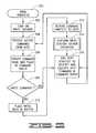
- FIG. 5is a flow chart for a DATA TRANSFER routine, generally illustrative of steps carried out by the disc drive in accordance with preferred embodiments of the present invention to transfer data between the disc drive and a host device.
- FIG. 6is a flow chart for an ADAPTIVE WRITE SCATTER GATHER routine that is a subroutine of the DATA TRANSFER routine of FIG. 5 .
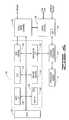
- FIG. 7provides a memory space representation of the disc drive buffer.
- FIG. 8generally illustrates a write skip mask formed in accordance with the routines of FIGS. 5 and 6.
- FIG. 9provides another memory space representation of the disc drive buffer.
- FIG. 10provides yet another memory space representation of the disc drive buffer.
- FIG. 1provides a top plan view of a disc drive 100 of the type used to store and retrieve computerized data.
- the disc drive 100includes a rigid base deck 102 that cooperates with a top cover 104 (shown in partial cutaway) to form a sealed housing for the drive. Electrical communication and control electronics are provided on a disc drive printed circuit board (PCB) affixed to the underside of the base deck 102 (and hence, not visible in FIG. 1 ).
- PCBprinted circuit board
- a spindle motor 106rotates a number of rigid data recording discs 108 at a constant high speed.
- a rotary actuator 110is positioned adjacent the discs 108 and supports a corresponding array of read/write data transducing heads 112 .
- the actuator 110is rotated through application of current to an actuator coil 114 of a voice coil motor (VCM) 116 .
- VCMvoice coil motor
- FIGS. 2 and 3generally illustrate the manner in which servo data are stored on the disc surfaces, the servo data enabling the servo control circuitry to detect head position and velocity in order to position the actuator in a desired relation to the discs.
- the servo dataare written using a servo track write (STW) process during disc drive manufacturing and are arranged in a plurality of radially extending servo wedges 118 .
- STWservo track write
- Each wedge 118comprises a plurality of adjacent servo fields 122 that are radially aligned to define each of the tracks on the disc surface (a portion of one such track is represented at 120 in FIGS. 2 and 3 ).
- User data fields 124are defined between adjacent servo fields 122 during a disc drive formatting operation. It will be recognized that the data sectors 124 are typically much longer than the servo fields 122 in order to maximize data capacity, so the aspect ratios and relative lengths of the fields in FIG. 3 are not represented to scale.
- the hostidentifies the data sectors 124 in the disc drive 100 through the assignment of a unique logical block address (LBA) to each data sector.
- LBAstypically range in consecutive order from 0 to n, with n constituting a large number (in the millions) depending upon the data storage capacity of the disc drive 100 . Consecutively numbered LBAs are typically physically proximate one another within the disc drive 100 .
- a typical LBA assignment strategyinvolves assigning consecutive LBA numbers to all of the data sectors 124 on a cylinder by cylinder basis (i.e., all of the tracks on the different discs 108 at a given radius). For example, LBA 0 can be assigned to a first data sector 124 at an outermost data track 120 on the top disc surface. The remaining data sectors 124 on this track can then be assigned successive LBA values (1, 2, 3, etc.). LBAs are then assigned to the data sectors 124 in the remaining tracks in the cylinder, and then to the data sectors in the next adjacent cylinder, and so on.
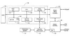
- FIG. 4provides a functional block diagram of relevant portions of the control circuitry of the disc drive 100 in conjunction with a host device 125 .
- FIG. 4shows the disc drive 100 to include a read/write channel 126 , a servo control circuit 128 with programmable digital signal processor (DSP) 130 , a top level control processor 132 (controller) with associated memory 134 , and interface hardware 136 .
- DSPdigital signal processor
- controller 132 , memory 134 and hardware 136are collectively referred to herein as a “hardware/firmware based interface circuit,” or just “interface circuit.”
- the read/write channel 126operates as a communication channel to encode input data to be written to the discs 108 and to decode amplified readback signals to reconstruct data retrieved from the discs 108 .
- the servo control circuit 128operates to demodulate head position and velocity from the servo data from the servo fields 122 (FIG. 3) and applies currents to rotate the actuator assembly 110 accordingly.
- the servo control circuit 128also provides drive currents to the spindle motor 106 to rotate the discs 108 at operational speed during drive operation.
- the control processor 132provides top level control for the disc drive 100 in accordance with programming steps stored in processor memory 134 and host commands provided by the host device 125 .
- the interface hardware 136includes a host interface (I/F) circuit 138 that controls the transfer of data and commands between the disc drive 100 and the host device 125 .
- a buffer 140 with a command queue 142temporarily stores data that are being transferred between the host and the discs 108 .
- a buffer control circuit 144controls the flow of data in and out of the buffer 140 .
- An error correction circuit (ECC) 146applies on-the-fly error detection and correction algorithms to the retrieved data to correct detected errors in the retrieved data in the buffer 140 .
- a disc control circuit 148sequences the read and write operations by the read/write channel 126 .
- a processor interface (I/F) 150provides a communication path with the control processor 132 .
- the interface circuituses the Small Computer System Interface (SCSI) host interface protocol, although such is not limiting to the scope of the invention as claimed below.
- SCSISmall Computer System Interface
- the command queue 142can concurrently store up to a maximum number of pending access commands from the host, such as 64 or 256.
- One type of access commandis a write command from the host to write a set of data loaded into the buffer 140 by the host to a selected sector 124 (FIG. 3) on a selected disc surface; another type of access command is a read command from the host to retrieve the contents of a selected sector 124 (FIG. 3) on a selected disc surface to the buffer 140 for subsequent transfer to the host.
- the hostidentifies the desired sectors 124 in terms of LBAs, and the control processor 132 converts each LBA to a physical block address (PBA) to identify the cylinder, disc surface and angular location of the desired sector.
- PBAphysical block address
- the flow chart of FIG. 5shows a DATA TRANSFER routine 200 , illustrative of steps carried out in accordance with preferred embodiments of the present invention to optimize the transfer of data from a host to the disc drive 100 .
- the interface circuitemploys adaptive, bi-directional write skip masks to combine multiple pending sets of writeback data into single writeback blocks which are then scheduled for execution at appropriate times.
- Each write skip maskgenerally comprises an interval of consecutive LBAs into which two or more sets of pending writeback data can be fitted.
- Each maskis preferably slidable and expandable, as desired.
- the label “write skip”generally refers to the fact that a small number of LBAs within the mask may exist between respective sets of writeback data; such intervening LBAs are “skipped over” after the conclusion of writing one set of writeback data and before the writing of another set of writeback data in the mask.
- write cachingis initially turned on during an initialization step at 202 .
- write cachinginvolves temporarily storing write data in the buffer 140 pending transfer of the write data to the discs at a later time, as opposed to immediately writing the data as when write caching is turned off.
- Receipt of each new access command by the disc drive 100 during normal operationis represented at step 204 .
- the host 125issues access commands from time to time at a rate and in an order as determined by the needs of the host. Thus, there can be times when access commands are issued relatively infrequently and other times when a large number of access commands are issued in rapid succession.
- Each read access commandidentifies the LBAs on the discs 108 the contents of which the host requires the disc drive 100 to retrieve.
- Each write access commandincludes the write data that the host requires the disc drive 100 to store and identifies the specific LBAs in which the disc drive is to store the write data.
- the interface circuitIn response to each new access command received at step 204 , the interface circuit creates a command node as a sortable access instruction in the command queue 142 , as shown by step 206 .
- Decision step 208inquires whether the new access command is a write command; if so, the interface circuit places the write data in the buffer 140 pending transfer to the discs (step 210 ) and reports to the host 125 that the write command has been completed (step 212 ). Steps 210 and 212 are not performed, of course, if the access command is a read command.
- the buffer 140is allocated among a number of variable length segments (such as 256 segments).
- the data associated with each access commandare generally assigned to a different segment within the buffer 140 .
- operation of step 212preferably includes placement of the write data into a selected segment.
- writebackFor purposes herein, such pending write data are also referred to herein as “writeback” data.
- the driveproceeds to inform the host that the write command has been completed even though the write data are actually still pending in the buffer.
- Advantages of this approachinclude the fact that the host will not make further inquiries to the drive or halt further processing as the host waits to hear that the write command has been completed.
- the observed data transfer rate(at the bus between host and drive) will be higher at that point since the drive immediately reports that the write command has been completed.
- a higher number of command nodeswill typically be present in the command queue 142 , allowing for statistically improved data transfer rates since more commands are available for selection at any given time.
- a disadvantage with write cachingis that the drive must schedule the write commands in the near future and will not get credit from a data transfer rate perspective for the time during which the write commands are actually executed. Thus, if a large number of pending write commands are allowed to accumulate, the observed service time can increase significantly as the drive transfers the accumulated writeback data from the buffer 140 to the discs 108 .
- step 214the flow of FIG. 5 continues to an ADAPTIVE WRITE SCATTER GATHER subroutine at step 214 which attempts to combine multiple, adjacent write command nodes into a single combined command node for more efficient processing of the data.
- the subroutine 214will be discussed in greater detail with regard to FIGS. 6-10.
- step 216a conventional sort strategy is performed to identify and execute the next appropriate command (read command, write command, or combined write command as provided by step 214 ).
- steps 204 and 216are asynchronous; new commands will be received from time to time at step 204 as dictated by the host 125 and the sort strategy step 216 will continue to sequentially select and execute command nodes in the command queue 142 so long as at least one command node remains in the queue.
- the routinefirst determines at step 218 whether two or more write command nodes (writeback commands) are presently pending in the command queue 142 . This step is performed since the routine requires at least two pending writeback commands before a combining of writeback commands can take place. If two or more writeback commands are not presently pending, the routine simply returns to the routine of FIG. 5 at step 220 .
- step 222the routine passes to step 222 where the newest (most recently received) writeback command is evaluated for inclusion into an existing write skip mask.
- FIG. 7has been provided to more clearly illustrate this step.
- FIG. 7is a generalized block representation of the buffer 140 and associated command queue 142 at a given instant in time during the operation of the routines of FIGS. 5 and 6.
- the buffer 140is represented as an addressable memory space in which various blocks of read and write data are temporarily stored.
- the bufferis also referred to as a first memory space; the discs 108 are also collectively referred to as a second memory space.
- the buffer 140is shown in FIG. 7 to include four sets of pending writeback data 224 , 226 , 228 and 230 respectively identified as WRITE DATA 1 through WRITE DATA 4 .
- These respective sets of writeback datarepresent blocks of data that have been provided with associated write commands from the host device 125 for transfer to the discs 108 , with WRITE DATA 4 representing the most recently received writeback data.
- no write skip maskshave been formed in the buffer 140 .
- Write command nodes (WRITE NODE 1 through WRITE NODE 4 ) for the sets of write data 224 , 226 , 228 and 230were generated and placed into the command queue 142 during the operation of step 206 in FIG. 5 as each new command was received in turn.
- the buffer 140is further shown in FIG. 7 to include a set of read data 232 (READ DATA 1 ), which represents read data associated with a read command from the host device 125 .
- the read data 232are temporarily stored in the buffer 140 pending completion of on-the-fly error detection and correction operations by the ECC block 146 (FIG. 4 ).
- a read command node READ 1 in the command queue 142is associated with this read command.
- the buffer 140further includes additional read data blocks including read on arrival (ROA) read data 234 and read look ahead (RLA) read data 236 .
- the ROA and RLA read data 234 , 236constitute read data that the drive 100 has proceeded to store in the buffer 140 without prompting by the host 125 on the basis that the host 125 might issue a request for such data in the near future.
- the various sets of write and read data 224 , 226 , 228 , 230 , 232 , 234 , 236represent various amounts of user data associated with different LBAs (data sectors 124 ) on the various disc surfaces, and which are stored in different segments (not separately denoted) at various locations within the memory space of the buffer 140 .
- actual writeback data setscan vary widely in size, for simplicity of illustration it will be contemplated that the writeback data sets 224 , 226 , 228 and 230 are each 20 LBAs in size.
- FIG. 8shows a bi-directional write skip mask 238 .
- the mask 238represents a moveable and expandable interval, or range of consecutive LBAs, within which two or more adjacent writeback data sets are placed to provide a single combined write command. Execution of a combined write command node results in the successive writing of the respective data sets during a single pass through the sort strategy step 216 in FIG. 5 .
- An advantage of the use of write skip masks such as 238is the reduction in the computational overhead required to separately sort and select the additional write command node(s) associated with the additional set(s) of data within a given mask.
- another advantage of the use of the adaptive, bi-directional masks such as 238is that writeback data from various commands received in descending order or in random order (with respect to LBA sequence) can be handled nominally as effectively as writeback data received in ascending order. It is contemplated that the interface circuit is configured to accommodate up to a selected number of masks at a given time (such as 32 masks).
- the sort strategy step 216Once the first set of writeback data within a given mask is selected by the sort strategy step 216 , all of the remaining writeback sets within the mask are automatically written in turn. Referring again to FIG. 6, since no preexisting masks have previously been formed among the WRITE DATA 1 , WRITE DATA 2 and WRITE DATA 3 data sets 224 , 226 and 228 , the answer to the inquiry at decision step 240 is no; that is, WRITE DATA 4 is not added to an existing mask. The flow then passes to step 242 when the WRITE DATA 4 set 230 is evaluated for creation of a new mask with any, some or all of the currently pending data sets 224 , 226 , 228 (WRITE DATA 1 , 2 , 3 ).
- the interface circuitcompares the range of LBAs associated with the newest selected set of writeback data (in this case WRITE DATA 4 230 ) with the range of LBAs associated with the remaining sets of write data (in this case 224 , 226 , 228 ) to determine whether the newest set of writeback data is within the mask interval of the existing set or sets of write data.
- This searchis both forward and backward in direction with respect to each remaining set of data 224 , 226 , 228 in turn.
- the 20 LBAs associated with the set of write data 224are LBAs 1001 to 1020 .
- the initial mask lengthis 100 LBAs.
- Centering the write data 224 within the mask 238provides an interval of consecutive LBAs from LBA 961 to LBA 1060 .
- This intervalincludes a first, leading portion 243 comprising LBAs 961 to 1000 and a second, trailing portion 245 comprising LBAs 1021 to 1060 .
- the operation of step 242(FIG. 6) preferably includes determining whether WRITE DATA 4 set 230 falls within the first and second portions 243 , 245 .
- the first and second portions 243 , 245are preferably adjustable in size; that is, the mask interval can be slidably moved with respect to the WRITE DATA 1 set of writeback data so that the first portion 243 is increased (or decreased) and the second portion 245 is correspondingly decreased (or increased). Stated another way, the WRITE DATA 1 can be shifted toward the front or toward the end of the mask interval as needed to increase the ability to encompass both the WRITE DATA 1 and the WRITE DATA 4 into a common mask.
- the fourth set of write data 230(WRITE DATA 4 ) shown in FIG. 7 constitutes LBAs 971 to 990 .
- the write data 230readily fits within the first portion 243 of the mask 238 .
- the routine 214thus proceeds to step 244 where the write skip mask is created.
- the interface circuitwill treat the data from LBA 971 to LBA 1020 as a single block of writeback data, and will skip over the intervening LBAs 991 to 1000 between WRITE DATA 4 and WRITE DATA 1 during the subsequent writing of the data.
- FIG. 9provides a depiction of the buffer 140 similar to that previously provided in FIG. 6 except that the WRITE DATA 4 set of write data 230 is now included within the mask 238 .
- the write data 230are shown to be moved to the upper left hand corner of the memory space, preferably no physical movement of the write data 230 within the memory is necessary for inclusion within the mask 238 .
- the mask 238can be thought of as a relational set. Pointers (not depicted) or other suitable methodologies can be used to link the data sets 228 , 230 with the mask 238 . Nevertheless, the reordering shown in FIG. 9 helps illustrate the results of the operation of step 244 in FIG. 6 .
- the routinepasses from decision step 244 to step 246 wherein the mask size is optionally adjusted by a selected amount, such as an additional 50 LBAs.
- a selected amountsuch as an additional 50 LBAs.
- Such expansionis shown in FIG. 8 to provide an expanded mask 248 , which now (in the current example) extends from LBA 936 to LBA 1085 .
- Expansion of the mask at step 246is optional, since the mask may already be of sufficient size to add additional write data. However, expansion is an attractive option in cases where LBAs of write data are close to the boundaries of the existing mask.
- a similar optional mask size expansion stepis shown at step 249 in FIG. 6 when writeback data are added to an existing mask (decision step 240 ). The routine then returns to the flow of FIG. 5 at step 220 .
- FIG. 10provides another representation of the buffer 140 in which the DATA WRITE 1 and DATA WRITE 4 sets 224 , 230 have been grouped together into the expanded write skip mask 248 .
- a second write skip mask 258is also shown in FIG. 10, with the second write skip mask 258 including the DATA WRITE 2 and DATA WRITE 3 sets 226 , 228 of FIGS. 6 and 9, as well as a new, fifth set of write data 260 .
- the WRITE DATA 5 set 260was found upon evaluation to fit between the WRITE DATA 2 and WRITE DATA 3 sets 226 , 228 .
- a sixth set of write data 262was subsequently added subjected to the routine of FIG. 6, but was not combined with either of the existing masks 248 , 258 .
- the interface circuitkeeps track of the respective sets of write data associated with each mask 248 , 258 and further tracks the order of the write data within each mask. Execution of the command node associated with the first set of write data in a given mask is automatically followed by execution of the remaining command nodes associated with the mask. For example, execution of the WRITE 4 command node (mask 248 in FIG. 10) results in the writing of the WRITE DATA 4 set of write data 230 (LBAs 971 through 990 ), immediately followed by the writing of the WRITE DATA 1 set of write data 224 (LBAs 1001 through 1020 ).
- the WRITE 4 command node and the WRITE 1 command nodeare treated as a single command node (such as combined node 264 in FIGS. 9 and 10 ) which requires only one selection operation to result in the writing of both sets of associated write data 230 , 224 .
- the WRITE 2 , WRITE 5 and WRITE 3 command nodes of FIG. 10are combined into a second combined command node 266 which is executed in an order determined in relation to the order of the LBAs of the respective data sets 226 , 260 and 228 within the mask 258 .
- the interface circuitcan be readily configured to leave the existing command nodes in the command queue 142 and track the combined nodes separately, or remove the existing command nodes from the command queue 142 and physically place a replacement combined command node (such as a WRITE NODE 1+4 command node) in the command queue 142 for sorting during step 216 (FIG. 5 ).
- a replacement combined command nodesuch as a WRITE NODE 1+4 command node
- a disc drive data storage device(such as 100 ) is provided with a first memory space (such as buffer 140 ) and a second memory space (such as discs 108 ).
- a host device(such as 125 ) issues access commands (such as by step 204 ) including first and second write commands to request writing of respective first and second sets of data (such as 224 , 230 ) to respective first and second sets of logical block addresses (LBAs) in the second memory space.
- An interface circuit(such as 132 , 134 , 136 ) of the data storage device temporarily stores the first and second sets of data in the first memory space pending transfer to the second memory space (such as by step 212 ).
- the interface circuitproceeds to sort the pending access commands in accordance with a sort strategy to increase data transfer performance (such as by step 216 ).
- the interface circuitoperates to implement an adaptive, bi-directional write skip mask (such as 238 ) comprising a selected interval of consecutive LBAs having a first portion (such as 243 ) which immediately precedes the first set of LBAs (such as 224 ) and a second portion (such as 245 ) which immediately follows the first set of LBAs.
- the maskis formed when the second set of LBAs fits within the first or second portion.
- the first and second write commandsare combined into a single combined write command (such as 264 , 266 ) which is scheduled for subsequent execution (such as by step 216 ).
- the combined write commandresults in the successive transfer of the first and second sets of data from the first memory space to the second memory space, wherein during said execution the first set of data is transferred followed by the second set of data when the second set of LBAs is encompassed within the second portion of the write skip mask, and wherein during said execution the second set of data is transferred followed by the first set of data when the second set of LBAs is encompassed within the first portion of the write skip mask.
- the interface circuitproceeds to separately execute the first and second write commands at different times (such as by step 216 ). Additional write skip masks are generated and evaluated for additional combinations of write commands as desired.
Landscapes
- Engineering & Computer Science (AREA)
- Theoretical Computer Science (AREA)
- Human Computer Interaction (AREA)
- Physics & Mathematics (AREA)
- General Engineering & Computer Science (AREA)
- General Physics & Mathematics (AREA)
- Signal Processing For Digital Recording And Reproducing (AREA)
Abstract
Description
Claims (16)
Priority Applications (1)
| Application Number | Priority Date | Filing Date | Title |
|---|---|---|---|
| US10/090,876US6732292B2 (en) | 2001-09-17 | 2002-03-04 | Adaptive bi-directional write skip masks in a data storage device |
Applications Claiming Priority (2)
| Application Number | Priority Date | Filing Date | Title |
|---|---|---|---|
| US32270201P | 2001-09-17 | 2001-09-17 | |
| US10/090,876US6732292B2 (en) | 2001-09-17 | 2002-03-04 | Adaptive bi-directional write skip masks in a data storage device |
Publications (2)
| Publication Number | Publication Date |
|---|---|
| US20030056060A1 US20030056060A1 (en) | 2003-03-20 |
| US6732292B2true US6732292B2 (en) | 2004-05-04 |
Family
ID=26782735
Family Applications (1)
| Application Number | Title | Priority Date | Filing Date |
|---|---|---|---|
| US10/090,876Expired - LifetimeUS6732292B2 (en) | 2001-09-17 | 2002-03-04 | Adaptive bi-directional write skip masks in a data storage device |
Country Status (1)
| Country | Link |
|---|---|
| US (1) | US6732292B2 (en) |
Cited By (6)
| Publication number | Priority date | Publication date | Assignee | Title |
|---|---|---|---|---|
| US20060195654A1 (en)* | 2005-02-28 | 2006-08-31 | Challener David C | Hard disk drive with write-only region |
| US20070283086A1 (en)* | 2006-06-06 | 2007-12-06 | Seagate Technology Llc | Write caching random data and sequential data simultaneously |
| US7478205B1 (en)* | 2006-07-12 | 2009-01-13 | Emc Corporation | Techniques for performing data operations spanning more than two data partitions |
| US8819308B1 (en)* | 2011-03-31 | 2014-08-26 | Emc Corporation | Pseudo writing system and method |
| US20150228317A1 (en)* | 2014-02-07 | 2015-08-13 | Micron Technology, Inc. | Apparatuses, memories, and methods for facilitating splitting of internal commands using a shared signal path |
| US12271622B2 (en) | 2021-01-13 | 2025-04-08 | Samsung Electronics Co., Ltd. | Processor using host memory buffer and storage system including the processor |
Families Citing this family (18)
| Publication number | Priority date | Publication date | Assignee | Title |
|---|---|---|---|---|
| US7346740B2 (en)* | 2002-11-01 | 2008-03-18 | Seagate Technology Llc | Transferring speculative data in lieu of requested data in a data transfer operation |
| DE10351599A1 (en)* | 2003-11-05 | 2005-06-16 | Tecpharma Licensing Ag | Auto-injection device |
| CN1906559B (en)* | 2003-12-30 | 2010-10-13 | 威步系统股份公司 | Method for controlling a data processing device |
| US20060265544A1 (en)* | 2005-05-17 | 2006-11-23 | John Rudelic | Internally authenticated flash remediation |
| US8473923B2 (en)* | 2007-09-12 | 2013-06-25 | Sandisk Technologies Inc. | Pointers for write abort handling |
| JP5147584B2 (en)* | 2008-07-23 | 2013-02-20 | 株式会社日立製作所 | Command execution method by storage subsystem and controller |
| US8006033B2 (en)* | 2008-09-09 | 2011-08-23 | Intel Corporation | Systems, methods, and apparatuses for in-band data mask bit transmission |
| TW201111986A (en)* | 2009-09-29 | 2011-04-01 | Silicon Motion Inc | Memory apparatus and data access method for memories |
| US9569351B2 (en) | 2010-10-25 | 2017-02-14 | Seagate Technology Llc | Storing corresponding data units in a common storage unit |
| US10353637B1 (en)* | 2011-12-30 | 2019-07-16 | EMC IP Holding Company LLC | Managing data storage |
| US9292337B2 (en)* | 2013-12-12 | 2016-03-22 | International Business Machines Corporation | Software enabled and disabled coalescing of memory transactions |
| US10133488B2 (en) | 2014-03-17 | 2018-11-20 | Primaryio, Inc. | Apparatus and method for cache provisioning, configuration for optimal application performance |
| US10146437B2 (en) | 2014-03-17 | 2018-12-04 | Primaryio, Inc. | Tier aware caching solution to increase application performance |
| US9740410B2 (en)* | 2014-03-17 | 2017-08-22 | Primaryio, Inc. | Maximize IO throughput in hybrid storage solution |
| US9489226B2 (en)* | 2014-06-06 | 2016-11-08 | PernixData, Inc. | Systems and methods to manage write commands in a cache |
| US9639287B1 (en)* | 2015-06-29 | 2017-05-02 | Western Digital Technologies, Inc. | Write command reporting |
| CN115994102A (en)* | 2021-10-18 | 2023-04-21 | 长鑫存储技术有限公司 | Write buffer circuit, data write method and memory |
| US11714645B2 (en) | 2021-10-18 | 2023-08-01 | Changxin Memory Technologies, Inc. | Write cache circuit, data write method, and memory |
Citations (12)
| Publication number | Priority date | Publication date | Assignee | Title |
|---|---|---|---|---|
| US5313626A (en) | 1991-12-17 | 1994-05-17 | Jones Craig S | Disk drive array with efficient background rebuilding |
| US5530829A (en) | 1992-12-17 | 1996-06-25 | International Business Machines Corporation | Track and record mode caching scheme for a storage system employing a scatter index table with pointer and a track directory |
| US5584007A (en) | 1994-02-09 | 1996-12-10 | Ballard Synergy Corporation | Apparatus and method for discriminating among data to be stored in cache |
| US5636355A (en) | 1993-06-30 | 1997-06-03 | Digital Equipment Corporation | Disk cache management techniques using non-volatile storage |
| US5664145A (en) | 1991-02-19 | 1997-09-02 | International Business Machines Corporation | Apparatus and method for transferring data in a data storage subsystems wherein a multi-sector data transfer order is executed while a subsequent order is issued |
| US5727183A (en) | 1995-03-15 | 1998-03-10 | Fujitsu Limited | Data transfer between disk storage and host device under the control of file control device employing cache and associated batch write-back operation |
| US5829018A (en) | 1994-10-25 | 1998-10-27 | International Business Machines Corporation | Apparatus and method for writing data from a cache to a storage device |
| US5875455A (en) | 1994-06-10 | 1999-02-23 | Matsushita Electric Industrial Co., Ltd. | Information recording and reproducing apparatus merging sequential recording requests into a single recording request, and method of data caching for such apparatus |
| US6164840A (en) | 1997-06-24 | 2000-12-26 | Sun Microsystems, Inc. | Ensuring consistency of an instruction cache with a store cache check and an execution blocking flush instruction in an instruction queue |
| US6189080B1 (en) | 1996-09-20 | 2001-02-13 | Emc Corporation | Minimum read rate throughput in a disk cache system |
| US20010032292A1 (en)* | 1999-12-03 | 2001-10-18 | Seagate Technology Llc | Implementation of skip mask hardware in a disc drive |
| US6470461B1 (en)* | 1999-06-07 | 2002-10-22 | Qlogic Corporation | Disk drive controller circuit and method for skipping defective and/or undesired sectors |
- 2002
- 2002-03-04USUS10/090,876patent/US6732292B2/ennot_activeExpired - Lifetime
Patent Citations (12)
| Publication number | Priority date | Publication date | Assignee | Title |
|---|---|---|---|---|
| US5664145A (en) | 1991-02-19 | 1997-09-02 | International Business Machines Corporation | Apparatus and method for transferring data in a data storage subsystems wherein a multi-sector data transfer order is executed while a subsequent order is issued |
| US5313626A (en) | 1991-12-17 | 1994-05-17 | Jones Craig S | Disk drive array with efficient background rebuilding |
| US5530829A (en) | 1992-12-17 | 1996-06-25 | International Business Machines Corporation | Track and record mode caching scheme for a storage system employing a scatter index table with pointer and a track directory |
| US5636355A (en) | 1993-06-30 | 1997-06-03 | Digital Equipment Corporation | Disk cache management techniques using non-volatile storage |
| US5584007A (en) | 1994-02-09 | 1996-12-10 | Ballard Synergy Corporation | Apparatus and method for discriminating among data to be stored in cache |
| US5875455A (en) | 1994-06-10 | 1999-02-23 | Matsushita Electric Industrial Co., Ltd. | Information recording and reproducing apparatus merging sequential recording requests into a single recording request, and method of data caching for such apparatus |
| US5829018A (en) | 1994-10-25 | 1998-10-27 | International Business Machines Corporation | Apparatus and method for writing data from a cache to a storage device |
| US5727183A (en) | 1995-03-15 | 1998-03-10 | Fujitsu Limited | Data transfer between disk storage and host device under the control of file control device employing cache and associated batch write-back operation |
| US6189080B1 (en) | 1996-09-20 | 2001-02-13 | Emc Corporation | Minimum read rate throughput in a disk cache system |
| US6164840A (en) | 1997-06-24 | 2000-12-26 | Sun Microsystems, Inc. | Ensuring consistency of an instruction cache with a store cache check and an execution blocking flush instruction in an instruction queue |
| US6470461B1 (en)* | 1999-06-07 | 2002-10-22 | Qlogic Corporation | Disk drive controller circuit and method for skipping defective and/or undesired sectors |
| US20010032292A1 (en)* | 1999-12-03 | 2001-10-18 | Seagate Technology Llc | Implementation of skip mask hardware in a disc drive |
Non-Patent Citations (3)
| Title |
|---|
| IBM Technical Disclosure Bulletin, Automated Hardware Processing of Direct Access Storage Device Skip Masks. May 1, 199 US. Vol. 39, Issue No. 5, pp. 121-122.* |
| IBM Technical Disclosure Bulletin, Method for Skip Write Emulation. Apr. 2001, UK. Issue No. 444, p. 636.** |
| IBM Technical Disclosure Bulletin, Skip Mask Operation in a No-ID Disk Drive. Jun. 1, 1996, US. Vol 39, Issue No. 6, pp. 47-50.** |
Cited By (9)
| Publication number | Priority date | Publication date | Assignee | Title |
|---|---|---|---|---|
| US20060195654A1 (en)* | 2005-02-28 | 2006-08-31 | Challener David C | Hard disk drive with write-only region |
| US8140795B2 (en) | 2005-02-28 | 2012-03-20 | Lenovo (Singapore) Pte. Ltd. | Hard disk drive with write-only region |
| US20070283086A1 (en)* | 2006-06-06 | 2007-12-06 | Seagate Technology Llc | Write caching random data and sequential data simultaneously |
| US8250316B2 (en) | 2006-06-06 | 2012-08-21 | Seagate Technology Llc | Write caching random data and sequential data simultaneously |
| US7478205B1 (en)* | 2006-07-12 | 2009-01-13 | Emc Corporation | Techniques for performing data operations spanning more than two data partitions |
| US8819308B1 (en)* | 2011-03-31 | 2014-08-26 | Emc Corporation | Pseudo writing system and method |
| US20150228317A1 (en)* | 2014-02-07 | 2015-08-13 | Micron Technology, Inc. | Apparatuses, memories, and methods for facilitating splitting of internal commands using a shared signal path |
| US9183904B2 (en)* | 2014-02-07 | 2015-11-10 | Micron Technology, Inc. | Apparatuses, memories, and methods for facilitating splitting of internal commands using a shared signal path |
| US12271622B2 (en) | 2021-01-13 | 2025-04-08 | Samsung Electronics Co., Ltd. | Processor using host memory buffer and storage system including the processor |
Also Published As
| Publication number | Publication date |
|---|---|
| US20030056060A1 (en) | 2003-03-20 |
Similar Documents
| Publication | Publication Date | Title |
|---|---|---|
| US6732292B2 (en) | Adaptive bi-directional write skip masks in a data storage device | |
| US6789163B2 (en) | Optimizing data transfer performance through partial write command purging in a disc drive | |
| US6968423B2 (en) | Dynamic data access pattern detection in a block data storage device | |
| US7783828B1 (en) | File system write to storage without specifying location reference | |
| US6606714B1 (en) | Disk drive using defect list to perform uninterrupted writing of non-relocated data blocks and caching of relocated data blocks for deferred writing | |
| US6499083B1 (en) | Disk-based storage system responsive to a direction-selection signal for autonomously controlling seeks in a sequence determined by the direction-selection signal and a locally-stored doubly linked list | |
| US6735678B2 (en) | Method and apparatus for disc drive defragmentation | |
| US6845405B1 (en) | Disk drive executing part of a linked disk command | |
| US6779081B2 (en) | Apparatus and method for defragmentation in disk storage system | |
| US6925539B2 (en) | Data transfer performance through resource allocation | |
| US5765204A (en) | Method and apparatus for adaptive localization of frequently accessed, randomly addressed data | |
| US8560759B1 (en) | Hybrid drive storing redundant copies of data on disk and in non-volatile semiconductor memory based on read frequency | |
| US6272565B1 (en) | Method, system, and program for reordering a queue of input/output (I/O) commands into buckets defining ranges of consecutive sector numbers in a storage medium and performing iterations of a selection routine to select and I/O command to execute | |
| US7076603B1 (en) | Method for mapping a selected sector to a zone on a disk | |
| US7046467B1 (en) | Method for generating a format specific data structure in a disk drive having differing surface formats | |
| KR20020064357A (en) | Buffer management system for managing the transfer of data into and out of a buffer in a disc drive | |
| US6925580B2 (en) | Full volume slip defect management in a disc drive | |
| US6898044B1 (en) | Method for calculating a format specific parameter in a disk drive having differing surface formats | |
| US9927981B2 (en) | Hybrid data storage device with partitioned local memory | |
| US7003626B1 (en) | Method for storing format specific data in a microcontroller execution memory | |
| US6957311B2 (en) | Data storage apparatus, computer apparatus, data processing apparatus, and data processing method | |
| US6868477B2 (en) | Method and apparatus for optimizing skip mask operations in a disc drive | |
| US6523086B1 (en) | Method for improving performance of read cache of magnetic disk drive | |
| US6219750B1 (en) | Disk drive having control mechanism to reduce or eliminate redundant write operations and the method thereof | |
| US6693754B2 (en) | Method and apparatus for a disc drive adaptive file system |
Legal Events
| Date | Code | Title | Description |
|---|---|---|---|
| AS | Assignment | Owner name:SEAGATE TECHNOLOGY LLC, CALIFORNIA Free format text:ASSIGNMENT OF ASSIGNORS INTEREST;ASSIGNORS:HERTZ, MARK D.;CLOUD, PHILIP E.;FOX, TRAVIS D.;AND OTHERS;REEL/FRAME:012672/0963 Effective date:20020304 | |
| AS | Assignment | Owner name:JPMORGAN CHASE BANK, AS COLLATERAL AGENT, NEW YORK Free format text:SECURITY AGREEMENT;ASSIGNOR:SEAGATE TECHNOLOGY LLC;REEL/FRAME:013177/0001 Effective date:20020513 Owner name:JPMORGAN CHASE BANK, AS COLLATERAL AGENT,NEW YORK Free format text:SECURITY AGREEMENT;ASSIGNOR:SEAGATE TECHNOLOGY LLC;REEL/FRAME:013177/0001 Effective date:20020513 | |
| FEPP | Fee payment procedure | Free format text:PAYOR NUMBER ASSIGNED (ORIGINAL EVENT CODE: ASPN); ENTITY STATUS OF PATENT OWNER: LARGE ENTITY | |
| STCF | Information on status: patent grant | Free format text:PATENTED CASE | |
| AS | Assignment | Owner name:SEAGATE TECHNOLOGY LLC, CALIFORNIA Free format text:RELEASE OF SECURITY INTERESTS IN PATENT RIGHTS;ASSIGNOR:JPMORGAN CHASE BANK, N.A. (FORMERLY KNOWN AS THE CHASE MANHATTAN BANK AND JPMORGAN CHASE BANK), AS ADMINISTRATIVE AGENT;REEL/FRAME:016958/0607 Effective date:20051130 | |
| FPAY | Fee payment | Year of fee payment:4 | |
| REMI | Maintenance fee reminder mailed | ||
| AS | Assignment | Owner name:WELLS FARGO BANK, NATIONAL ASSOCIATION, AS COLLATERAL AGENT AND SECOND PRIORITY REPRESENTATIVE, CALIFORNIA Free format text:SECURITY AGREEMENT;ASSIGNORS:MAXTOR CORPORATION;SEAGATE TECHNOLOGY LLC;SEAGATE TECHNOLOGY INTERNATIONAL;REEL/FRAME:022757/0017 Effective date:20090507 Owner name:JPMORGAN CHASE BANK, N.A., AS ADMINISTRATIVE AGENT AND FIRST PRIORITY REPRESENTATIVE, NEW YORK Free format text:SECURITY AGREEMENT;ASSIGNORS:MAXTOR CORPORATION;SEAGATE TECHNOLOGY LLC;SEAGATE TECHNOLOGY INTERNATIONAL;REEL/FRAME:022757/0017 Effective date:20090507 Owner name:JPMORGAN CHASE BANK, N.A., AS ADMINISTRATIVE AGENT Free format text:SECURITY AGREEMENT;ASSIGNORS:MAXTOR CORPORATION;SEAGATE TECHNOLOGY LLC;SEAGATE TECHNOLOGY INTERNATIONAL;REEL/FRAME:022757/0017 Effective date:20090507 Owner name:WELLS FARGO BANK, NATIONAL ASSOCIATION, AS COLLATE Free format text:SECURITY AGREEMENT;ASSIGNORS:MAXTOR CORPORATION;SEAGATE TECHNOLOGY LLC;SEAGATE TECHNOLOGY INTERNATIONAL;REEL/FRAME:022757/0017 Effective date:20090507 | |
| AS | Assignment | Owner name:SEAGATE TECHNOLOGY HDD HOLDINGS, CALIFORNIA Free format text:RELEASE;ASSIGNOR:JPMORGAN CHASE BANK, N.A., AS ADMINISTRATIVE AGENT;REEL/FRAME:025662/0001 Effective date:20110114 Owner name:SEAGATE TECHNOLOGY INTERNATIONAL, CALIFORNIA Free format text:RELEASE;ASSIGNOR:JPMORGAN CHASE BANK, N.A., AS ADMINISTRATIVE AGENT;REEL/FRAME:025662/0001 Effective date:20110114 Owner name:MAXTOR CORPORATION, CALIFORNIA Free format text:RELEASE;ASSIGNOR:JPMORGAN CHASE BANK, N.A., AS ADMINISTRATIVE AGENT;REEL/FRAME:025662/0001 Effective date:20110114 Owner name:SEAGATE TECHNOLOGY LLC, CALIFORNIA Free format text:RELEASE;ASSIGNOR:JPMORGAN CHASE BANK, N.A., AS ADMINISTRATIVE AGENT;REEL/FRAME:025662/0001 Effective date:20110114 | |
| AS | Assignment | Owner name:THE BANK OF NOVA SCOTIA, AS ADMINISTRATIVE AGENT, CANADA Free format text:SECURITY AGREEMENT;ASSIGNOR:SEAGATE TECHNOLOGY LLC;REEL/FRAME:026010/0350 Effective date:20110118 Owner name:THE BANK OF NOVA SCOTIA, AS ADMINISTRATIVE AGENT, Free format text:SECURITY AGREEMENT;ASSIGNOR:SEAGATE TECHNOLOGY LLC;REEL/FRAME:026010/0350 Effective date:20110118 | |
| FPAY | Fee payment | Year of fee payment:8 | |
| AS | Assignment | Owner name:SEAGATE TECHNOLOGY US HOLDINGS, INC., CALIFORNIA Free format text:TERMINATION AND RELEASE OF SECURITY INTEREST IN PATENT RIGHTS;ASSIGNOR:WELLS FARGO BANK, NATIONAL ASSOCIATION, AS COLLATERAL AGENT AND SECOND PRIORITY REPRESENTATIVE;REEL/FRAME:030833/0001 Effective date:20130312 Owner name:SEAGATE TECHNOLOGY INTERNATIONAL, CAYMAN ISLANDS Free format text:TERMINATION AND RELEASE OF SECURITY INTEREST IN PATENT RIGHTS;ASSIGNOR:WELLS FARGO BANK, NATIONAL ASSOCIATION, AS COLLATERAL AGENT AND SECOND PRIORITY REPRESENTATIVE;REEL/FRAME:030833/0001 Effective date:20130312 Owner name:EVAULT INC. (F/K/A I365 INC.), CALIFORNIA Free format text:TERMINATION AND RELEASE OF SECURITY INTEREST IN PATENT RIGHTS;ASSIGNOR:WELLS FARGO BANK, NATIONAL ASSOCIATION, AS COLLATERAL AGENT AND SECOND PRIORITY REPRESENTATIVE;REEL/FRAME:030833/0001 Effective date:20130312 Owner name:SEAGATE TECHNOLOGY LLC, CALIFORNIA Free format text:TERMINATION AND RELEASE OF SECURITY INTEREST IN PATENT RIGHTS;ASSIGNOR:WELLS FARGO BANK, NATIONAL ASSOCIATION, AS COLLATERAL AGENT AND SECOND PRIORITY REPRESENTATIVE;REEL/FRAME:030833/0001 Effective date:20130312 | |
| FPAY | Fee payment | Year of fee payment:12 | |
| AS | Assignment | Owner name:SEAGATE TECHNOLOGY PUBLIC LIMITED COMPANY, CALIFORNIA Free format text:RELEASE BY SECURED PARTY;ASSIGNOR:THE BANK OF NOVA SCOTIA;REEL/FRAME:072193/0001 Effective date:20250303 Owner name:SEAGATE TECHNOLOGY, CALIFORNIA Free format text:RELEASE BY SECURED PARTY;ASSIGNOR:THE BANK OF NOVA SCOTIA;REEL/FRAME:072193/0001 Effective date:20250303 Owner name:SEAGATE TECHNOLOGY HDD HOLDINGS, CALIFORNIA Free format text:RELEASE BY SECURED PARTY;ASSIGNOR:THE BANK OF NOVA SCOTIA;REEL/FRAME:072193/0001 Effective date:20250303 Owner name:I365 INC., CALIFORNIA Free format text:RELEASE BY SECURED PARTY;ASSIGNOR:THE BANK OF NOVA SCOTIA;REEL/FRAME:072193/0001 Effective date:20250303 Owner name:SEAGATE TECHNOLOGY LLC, CALIFORNIA Free format text:RELEASE BY SECURED PARTY;ASSIGNOR:THE BANK OF NOVA SCOTIA;REEL/FRAME:072193/0001 Effective date:20250303 Owner name:SEAGATE TECHNOLOGY INTERNATIONAL, CAYMAN ISLANDS Free format text:RELEASE BY SECURED PARTY;ASSIGNOR:THE BANK OF NOVA SCOTIA;REEL/FRAME:072193/0001 Effective date:20250303 Owner name:SEAGATE HDD CAYMAN, CAYMAN ISLANDS Free format text:RELEASE BY SECURED PARTY;ASSIGNOR:THE BANK OF NOVA SCOTIA;REEL/FRAME:072193/0001 Effective date:20250303 Owner name:SEAGATE TECHNOLOGY (US) HOLDINGS, INC., CALIFORNIA Free format text:RELEASE BY SECURED PARTY;ASSIGNOR:THE BANK OF NOVA SCOTIA;REEL/FRAME:072193/0001 Effective date:20250303 |