US6732234B1 - Direct access mode for a cache - Google Patents
Direct access mode for a cacheDownload PDFInfo
- Publication number
- US6732234B1 US6732234B1US09/633,544US63354400AUS6732234B1US 6732234 B1US6732234 B1US 6732234B1US 63354400 AUS63354400 AUS 63354400AUS 6732234 B1US6732234 B1US 6732234B1
- Authority
- US
- United States
- Prior art keywords
- transaction
- cache
- entry
- address
- recited
- Prior art date
- Legal status (The legal status is an assumption and is not a legal conclusion. Google has not performed a legal analysis and makes no representation as to the accuracy of the status listed.)
- Expired - Fee Related, expires
Links
Images


Classifications
- G—PHYSICS
- G06—COMPUTING OR CALCULATING; COUNTING
- G06F—ELECTRIC DIGITAL DATA PROCESSING
- G06F12/00—Accessing, addressing or allocating within memory systems or architectures
- G06F12/02—Addressing or allocation; Relocation
- G06F12/08—Addressing or allocation; Relocation in hierarchically structured memory systems, e.g. virtual memory systems
- G06F12/0802—Addressing of a memory level in which the access to the desired data or data block requires associative addressing means, e.g. caches
- G06F12/0864—Addressing of a memory level in which the access to the desired data or data block requires associative addressing means, e.g. caches using pseudo-associative means, e.g. set-associative or hashing
- G—PHYSICS
- G06—COMPUTING OR CALCULATING; COUNTING
- G06F—ELECTRIC DIGITAL DATA PROCESSING
- G06F12/00—Accessing, addressing or allocating within memory systems or architectures
- G06F12/02—Addressing or allocation; Relocation
- G06F12/08—Addressing or allocation; Relocation in hierarchically structured memory systems, e.g. virtual memory systems
- G06F12/0802—Addressing of a memory level in which the access to the desired data or data block requires associative addressing means, e.g. caches
- G06F12/0893—Caches characterised by their organisation or structure
- G06F12/0895—Caches characterised by their organisation or structure of parts of caches, e.g. directory or tag array
- G—PHYSICS
- G06—COMPUTING OR CALCULATING; COUNTING
- G06F—ELECTRIC DIGITAL DATA PROCESSING
- G06F2212/00—Indexing scheme relating to accessing, addressing or allocation within memory systems or architectures
- G06F2212/25—Using a specific main memory architecture
- G06F2212/251—Local memory within processor subsystem
- G06F2212/2515—Local memory within processor subsystem being configurable for different purposes, e.g. as cache or non-cache memory
Definitions
- This inventionis related to digital systems and, more particularly, to caches within digital systems.
- a cacheis a relatively small, high speed memory which may store copies of data corresponding to various recently-accessed memory locations.
- cache storageis allocated and deallocated in units of cache lines (a group of bytes from contiguous memory locations).
- the cachemay include multiple entries, and each entry may include storage for a cache line of bytes. If requested data for an access is not in the cache (a “miss”), an entry is allocated for the cache line including the requested data and the cache line is filled into the allocated entry. Subsequently, the data may be found in the cache upon request (a “hit”).
- a portion of the cache line(often called a “sector”) may be valid while other portions are invalid. However, the entire cache entry is allocated for the cache line if one or more of the sectors are valid.
- the testing of memorieshas been performed by including-hardware embedded in the memory or situated close to the memory to perform the testing.
- This hardwareis typically referred to as built-in self test (BIST) hardware. Since the BIST hardware is used only for testing purposes, the BIST hardware must be as small (in terms of circuit area, e.g. numbers of transistors) as possible to minimize the cost of the BIST hardware. Thus, the testing strategies that may be applied by BIST hardware have generally been limited to those strategies that can be implemented using a minimal amount of hardware. Furthermore, if the BIST hardware itself is implemented incorrectly, false failures or incomplete test coverage may result. A more flexible method for testing a memory is therefore desired.
- the cacheis configured to receive direct access transactions.
- Each direct access transactionexplicitly specifies a cache storage entry to be accessed in response to the transaction.
- the cachemay access the cache storage entry (bypassing the normal tag comparisons and hit determination used for memory transactions) and either read the data from the cache storage entry (for read transactions) or write data from the transaction to the cache storage entry (for write transactions).
- the direct access transactionsmay, for example, be used to perform testing of the cache memory.
- Direct access transactionsmay be used to read and/or write test data from specific cache entries.
- BIST hardwaremay be eliminated in favor of performing testing of the cache using direct access transactions. Accordingly, risks due to faulty implementation of the test strategy in hardware may be alleviated. If an error in the test implementation is made, the error may be corrected by changing the test transactions.
- a processormay be used to initiate the direct access transactions by executing a code sequence.
- flexibilitymay be achieved in the test algorithms used by coding appropriate code sequences. More complex test algorithms may be more readily implemented using such a testing strategy than may be used for BIST hardware, since the requirement to keep the BIST hardware small and simple may be eliminated.
- testingmay be performed by any device capable of communicating with the cache. Accordingly, even if the processor is not functioning properly, the cache may be tested by another device.
- direct access transactionsmay be used to perform a reset of the cache (by writing known data to each cache entry).
- circuitry for ensuring that the cache resets to a known statemay be eliminated.
- ECCerror checking and correction
- the ECC datamay be initialized during the writing of data in response to the direct access transactions, eliminated spurious ECC errors that might occur if uninitialized data were read from the cache.
- Direct access write transactionscould also be used to recover from uncorrectable ECC errors, by overwriting the failing data to eliminate the errant data.
- the cachemay alter the state of its replacement policy in response to a direct access transaction explicitly specifying a particular way of the cache.
- the statemay be altered such that a succeeding cache miss causes an eviction of the particular way.
- Such an embodimentmay be used to enhance the test coverage achievable with direct access transactions by providing the flexibility of using memory transactions to store test data into the cache. Testing of tag information may be more thorough in such an embodiment.
- the combination of direct access transactions and the deterministic setting of the replacement policymay have other uses (e.g. for flushing a cache entry or all cache entries without requiring an explicit flush command).
- a cacheis contemplated.
- the cacheincludes a memory and a control circuit coupled to the memory.
- the memoryincludes a plurality of entries. Each of the plurality of entries is configured to store a cache line of data.
- the control circuitis configured to select a first entry of the plurality of entries for access responsive to a first transaction which explicitly specifies the first entry.
- a systemincluding a cache and a first circuit coupled to the cache.
- the cacheincludes a plurality of entries. Each of the plurality of entries is configured to store a cache line of data.
- the first circuitis configured to initiate a first transaction explicitly specifying a first entry of the plurality of entries.
- the cacheis configured to select the first entry for access responsive to the first transaction.
- a method for testing a cacheis also contemplated.
- a first transactionis performed to cause first data to be stored in a first entry of a cache.
- a read transactionexplicitly specifying the first entry subsequent to performing the first transaction.
- the second data returned in response to the read transactionis compared to the first data to detect if an error occurred in the first entry.
- FIG. 1is a block diagram of one embodiment of a system.
- FIG. 2is a block diagram of one embodiment of a cache shown in FIG. 1 .
- FIG. 3is a block diagram of one embodiment of an address from a memory address space and one embodiment of an address from a direct access address space.
- FIG. 4is a flowchart illustrating operation of one embodiment of the cache shown in FIGS. 1 and 2 for a read transaction.
- FIG. 5is a flowchart illustrating operation of one embodiment of the cache shown in FIGS. 1 and 2 for a write transaction.
- FIG. 6is a block diagram of one embodiment of a replacement circuit shown in FIG. 2 .
- FIG. 7is a flowchart illustrating operation of one embodiment of a control unit shown in FIG. 6 .
- FIG. 8is a flowchart illustrating one embodiment of testing the cache shown in FIGS. 1 and 2.
- FIG. 9is a flowchart illustrating one embodiment of resetting the cache shown in FIGS. 1 and 2.
- FIG. 10is a flowchart illustrating one embodiment of synchronization of the cache shown in FIGS. 1 and 2.
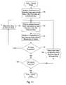
- FIG. 11is a flowchart illustrating one embodiment of flushing the cache shown in FIGS. 1 and 2.
- FIG. 12is a flowchart illustrating one embodiment of flushing one cache line shown in FIGS. 1 and 2.
- FIG. 13is a block diagram of an exemplary carrier medium.
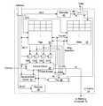
- system 10includes processors 12 A- 12 B, an L2 cache 14 , a memory controller 16 , a high speed input/output (I/O) bridge 18 , an I/O bridge 20 , and I/O interfaces 22 A- 22 B.
- System 10may include a bus 24 for interconnecting the various components of system 10 .
- processors 12 A- 12 B, L2 cache 14 , memory controller 16 , high speed I/O bridge 18 and I/O bridge 20are coupled to bus 24 .
- I/O bridge 20is coupled to I/O interfaces 22 A- 22 B.
- L2 cache 14is coupled to memory controller 16 , which is further coupled to a memory 26 .
- processors 12 A- 12 B and/or the I/O bridges/interfacesmay initiate transactions on the bus 24 .
- Transactionsmay include read transactions (transfers of data to the transaction initiator) and write transactions (transfers of data from the transaction initiator).
- Transactionsmay further include various coherency commands (e.g. an invalidate command) which may or may not involve a transfer of data.
- System 10supports various types of transactions on bus 24 . Memory transactions are transactions which target a memory location. Additionally, system 10 supports direct access transactions to L2 cache 14 . As used herein, the term “direct access transaction” refers to a transaction which targets an entry in L2 cache 14 and explicitly specifies that entry. If the direct access transaction is a read, the data in the specified entry is returned by L2 cache 14 . If the direct access transaction is a write, the data provided in the write transaction is stored in the entry. System 10 may further support I/O transactions and configuration transactions on bus 24 .
- An addressable range of system 10is defined by the size of the addresses which may be transmitted on bus 24 .
- the addressable rangemay be divided into several address spaces including a memory address space, a direct access address space, an I/O address space, and various configuration address spaces.
- the address space which includes the address of a transactionmay identify the type of the transaction.
- an address within the memory address spaceindicates that the transaction is a memory transaction and the address identifies a targeted memory location in memory 26 (and thus memory controller 16 and L2 cache 14 may respond to the transaction).
- An address within the I/O memory mapped address spaceindicates that the transaction is an I/O transaction and the address targets an I/O device on one of the I/O interfaces.
- An address within the configuration address spaceindicates that the transaction is a configuration transaction and the address targets various configuration registers in devices within system 10 .
- An address within the direct access address spaceindicates that the transaction is a direct access transaction and the address specifies the entry of L2 cache 14 to be directly accessed by the direct access transaction.
- the entry (if any) of L2 cache 14 accessed to store or return data for the memory transactionis determined by comparing the tags of cache lines stored in the entries to the address of the memory transaction.
- direct access transactionsexplicitly specify the entry to be accessed. L2 cache 14 may access the specified entry without regard to the tag comparisons normally used to select the accessed entry.
- direct access transactionsmay transfer an entire cache line of data. However, other embodiments may transfer a portion of a cache line in response to direct access transactions.
- command type encodingscould be provided on control signals transmitted during the address portion of the transaction.
- L2 cache 14may be tested for defects by any device attached to bus 24 .
- the devicemay initiate direct access transactions to read and write the entries of L2 cache 14 .
- Test datamay be written, and then read back and checked to ensure that no errors occurred in storing of the test data in the specified entry.
- Each entrymay be tested in this manner.
- processors 12 A- 12 Bmay execute a code sequence which performs the desired tests. Since the tests are performed via software, the test algorithm is flexible and may easily be changed. The problem of incorrectly implementing a test algorithm in BIST hardware may thus be eliminated. Additionally, since software is used to implement the test instead of BIST hardware, there may be more flexibility in the algorithms that can be used since the requirement to keep the hardware small is eliminated.
- any device attached to the bus 24may be used to perform the test.
- the direct access address spaceis located within 32 bits of address (i.e. more significant bits than the 32 bits are zero), which allows any device capable of generating 32 bits of address to perform direct access transactions.
- a device on the PCI busone example of an I/O interface
- direct access transactionsmay have over attempting to use memory transactions to perform testing is that, if an entry has a defect in the tag portion of the entry, it may be difficult to get a hit in that entry (since the tag is stored in a faulty manner). By using direct access transactions, the hit circuitry is ignored and the specified entry is accessed.
- L2 cache 14may employ error checking and correction (ECC) to protect the tags and/or data in the cache. If an uncorrectable ECC error is detected, a direct access write transaction may be used to overwrite the entry for which the error is detected. In this manner, the data in error may be eliminated from the cache. ECC bits corresponding to the data being written may be generated and stored by L2 cache 14 in response to the direct access write transaction.
- ECCerror checking and correction
- L2 cache 14includes a replacement circuit implementing the replacement policy of the cache.
- the replacement circuitmay, in response to a direct access transaction specifying a first way, establish a state corresponding to the first way. If the next transaction is a memory transaction which misses L2 cache 14 , the first way may be selected from the addressed set for eviction. In this manner, the way selected for the next memory transaction is deterministic.
- the replacement circuitmay establish a state responsive to other types of transactions than direct access transactions. For example, the replacement circuit may be memory-mapped for a write transaction to a predetermined address, and the data in the write transaction may indicate the desired state (or the first way). As another example, a dedicated bus command could be used to convey the state or the first way.
- the deterministic setting of the replacement policymay be used for enhanced testing. Since the direct access transactions, in one embodiment, are determined from an address space, some of the address bits in the tag of the entry may not be varied using direct access write transactions. Thus, a direct access transaction to the desired way may be performed, followed by a memory transaction (which misses the cache) to the desired index. The miss by the memory transaction causes an eviction to store the cache line addressed by the memory transaction, and the evicted cache line is from the desired way. The tag is updated with the address of the memory transaction. Subsequently, a direct access read transaction may be performed, and the tag may be captured by the above mentioned register. The tag may be checked to ensure it was stored without error. Thus, additional freedom in varying the tag bits may be achieved.
- the deterministic setting of the replacement policymay have other uses as well.
- the deterministic settingmay be used, after various initialization procedures have been performed, to provide a synchronization point for the replacement policy. This may be useful in validation, especially if similar tests are to be run in different test environments. Furthermore, controlling which entry will be used for a miss may be useful generally in validation testing. Additionally, the deterministic setting may be used to flush L2 cache 14 without requiring an explicit flush command on bus 24 . Instead, sequences of a direct access transaction (to set the replacement policy) followed by a memory transaction which misses (to evict the cache line in the selected way) may be used to flush the cache.
- the replacement policy of L2 cache 14is a pseudo-random policy (also referred to simply as random).
- a “pseudo-random” policythe replacement circuit sequences through a set of states, and the state existing when a particular miss is detected determines the way selected for eviction.
- a statemay be established consistent with selection of the way identified by the direct access transaction to provide determinism for a succeeding eviction.
- LRU policy for the index identified by the direct access transactionmay be set to indicate that the way identified by the direct access transaction is least recently used.
- a subsequent miss to the same indexmay generate an eviction of the way identified by the direct access transaction.
- Processors 12 A- 12 Bmay be designed to any instruction set architecture, and may execute programs written to that instruction set architecture.
- Exemplary instruction set architecturesmay include the MIPS instruction set architecture (including the MIPS-3D and MIPS MDMX application specific extensions), the IA-32 or IA-64 instruction set architectures developed by Intel Corp., the PowerPC instruction set architecture, the Alpha instruction set architecture, the ARM instruction set architecture, or any other instruction set architecture.
- L2 cache 14is a high speed cache memory.
- L2 cache 14is referred to as “L2” since processors 12 A- 12 B may employ internal level 1 (“L1”) caches. If L1 caches are not included in processors 12 A- 12 B, L2 cache 14 may be an L1 cache. Furthermore, if multiple levels of caching are included in processors 12 A- 12 B, L2 cache 14 may be a lower level cache than L2.
- L2 cache 14may employ any organization, including direct mapped, set associative, and fully associative organizations. In one particular implementation, L2 cache 14 may be a 512 kilobyte, 4 way set associative cache having 32 byte cache lines.
- a set associative cacheis a cache arranged into multiple sets, each set comprising two or more entries.
- a portion of the address(the “index”) is used to select one of the sets (i.e. each encoding of the index selects a different set).
- the entries in the selected setare eligible to store the cache line accessed by the address.
- Each of the entries within the setis referred to as a “way” of the set.
- the portion of the address remaining after removing the index (and the offset within the cache line)is referred to as the “tag”, and is stored in each entry to identify the cache line in that entry.
- the stored tagsare compared to the corresponding tag portion of the address of a memory transaction to determine if the memory transaction hits or misses in the cache, and is used to select the way in which the hit is detected (if a hit is detected).
- Memory controller 16is configured to access memory 26 in response to memory transactions received on bus 24 .
- Memory controller 16receives a hit signal from L2 cache 14 , and if a hit is detected in L2 cache 14 for a memory transaction, memory controller 16 does not respond to that memory transaction. If a miss is detected by L2 cache 14 , or the memory transaction is non-cacheable, memory controller 16 may access memory 26 to perform the read or write operation.
- Memory controller 16may be designed to access any of a variety of types of memory. For example, memory controller 16 may be designed for synchronous dynamic random access memory (SDRAM), and more particularly double data rate (DDR) SDRAM. Alternatively, memory controller 16 may be designed for DRAM, Rambus DRAM (RDRAM), SRAM, or any other suitable memory device.
- SDRAMsynchronous dynamic random access memory
- DDRdouble data rate SDRAM
- RDRAMRambus DRAM
- SRAMSRAM
- High speed I/O bridge 18may be an interface to a high speed I/O interconnect.
- high speed I/O bridge 18may implement the Lightning Data Transport (LDT) I/O fabric developed by Advanced Micro Devices, Inc.
- LDTLightning Data Transport
- Other high speed interfacesmay be alternatively used.
- I/O bridge 20is used to link one or more I/O interfaces (e.g. I/O interfaces 22 A- 22 B) to bus 24 .
- I/O bridge 20may serve to reduce the electrical loading on bus 24 if more than one I/O interface 22 A- 22 B is bridged by I/O bridge 20 .
- I/O bridge 20performs transactions on bus 24 on behalf of I/O interfaces 22 A- 22 B and relays transactions targeted at an I/O interface 22 A- 22 B from bus 24 to that I/O interface 22 A- 22 B.
- I/O interfaces 22 A- 22 Bmay be lower bandwidth, higher latency interfaces.
- I/O interfaces 22 A- 22 Bmay include one or more serial interfaces, Personal Computer Memory Card International Association (PCMCIA) interfaces, Ethernet interfaces (e.g. media access control level interfaces), Peripheral Component Interconnect (PCI) interfaces, etc.
- PCMCIAPersonal Computer Memory Card International Association
- Ethernet interfacese.g. media access control level interfaces
- PCIPeripheral Component Interconnect
- Bus 24may have any suitable protocol and construction.
- bus 24may be a split transaction bus.
- the implementationmay include an address bus supporting up to 40 bits of addressable range and a data bus capable of transmitting one cache line per clock cycle (e.g. 32 bytes). Other widths for either the address bus or data bus are possible and contemplated.
- the busmay also include transactions to support maintaining memory coherency (e.g. an invalidate command).
- the busmay use any suitable signalling technique (e.g. differential or non-differential signalling).
- system 10(and more particularly processors 12 A- 12 B, L2 cache 14 , memory controller 16 , I/O interfaces 22 A- 22 B, I/O bridge 20 , I/O bridge 18 and bus 24 may be integrated onto a single integrated circuit as a system on a chip configuration.
- memory 26may be integrated as well.
- one or more of the componentsmay be implemented as separate integrated circuits, or all components may be separate integrated circuits, as desired. Any level of integration may be used.
- a transaction“targets” a location or device if the location or device is the provider of data for the transaction (for a read transaction) or receiver of data for the transaction (for a write transaction). Viewed in another way, a transaction may target a location or device if the address of the transaction is mapped to that location or device.
- L2 cache 14includes a tags memory 30 , a data memory 32 , a set of comparators 34 A- 34 D, a control circuit 36 , a pair of decoders 38 and 40 , a tag register 42 , a replacement circuit 44 , and multiplexors (muxes) 46 and 48 .
- Tags memory 30 and data memory 32are each coupled to receive an index portion of the address of a transaction (the address of the transaction may be referred to herein as the “input address”).
- Data memory 32is coupled to receive and provide data corresponding to the transaction.
- Tags memory 30is further coupled to receive a tag portion of the input address, and is coupled to comparators 34 A- 34 D and mux 46 .
- Comparators 34 A- 34 Dare further coupled to receive the tag portion of the input address and are coupled to control circuit 36 .
- Control circuit 36is coupled to receive a portion of the input address, control information corresponding to a transaction, and a direct access signal from decoder 38 .
- Control circuit 36is coupled to provide a way selection to tags memory 30 , data memory 32 , and mux 46 .
- Control circuit 36is further coupled to provide control signals to tags memory 30 and data memory 32 , and is coupled to provide a hit signal to memory controller 16 .
- Control circuit 36is still further coupled to tag register 42 and replacement circuit 44 , which is further coupled to receive a portion of the input address and the direct access signal from decoder 38 .
- Tag register 42is coupled to receive the direct access signal and is coupled to mux 48 .
- Decoders 38 and 40are coupled to receive a portion of the input address, and decoder 40 is coupled to mux 48 .
- tags memory 30stores the tag information for each entry in L2 cache 14
- data memory 32stores the cache line of data for each entry in L2 cache 14
- an entrycomprises a tag memory storage location and a data memory storage location.
- the tag memory storage locationstores the tag for the entry (and possibly other information, such as validity and dirty information).
- the tag information for an entryincludes the tag portion of the address (e.g. bits 39 : 17 in the illustrated embodiment), a valid bit indicating the validity or lack of validity of the entry, and a dirty bit indicating the dirty or clean state of the cache line.
- a cache lineis dirty if at least one byte of the cache line has been modified in L2 cache 14 and the modification has not been written to memory 26 .
- the data memory storage locationstores the cache line of data in the entry.
- the index portion of the input address(e.g. bits 16 : 5 in the illustrated embodiment) is provided to tags memory 30 and data memory 32 .
- Each memoryselects a set of storage locations in response to the index.
- Tags memory 30outputs the tag from each selected storage location to comparators 34 A- 34 D, which compare the tags to the tag portion of the input address. If the tag compares equally, and the entry is valid, the corresponding comparator 34 A- 34 D may signal a hit to control circuit 36 .
- Control circuit 36may assert the hit signal to memory controller 16 if any of the comparators 34 A- 34 D indicates a hit, and may determine a way selection from the output of comparators 34 A- 34 D as well.
- Each comparator 34 A- 34 Dis comparing the tag from a different way of L2 cache 14 , and thus the comparator output indicating a hit is an indication of the hitting way.
- Control circuit 36provides the way selection to tags memory 30 and data memory 32 .
- Data memory 32provides data from the storage location at the selected index and way, or receives data into that storage location, depending upon whether the memory transaction is a read or write transaction.
- Control circuit 36receives the control information corresponding to the transaction, and generates control signals for data memory 32 and tags memory 30 .
- the control signalsmay include, for example, an enable signal and a read/write signal to indicate whether the memory is to read or write.
- Tags memory 30may be updated in response to the transaction as well. For example, if the transaction is a write, the dirty bit in the hitting entry may be updated. Additionally, if the transaction is a miss in L2 cache 14 and is cacheable, L2 cache 14 may select a way for eviction to receive a line fill of the missing line. More particularly, replacement circuit 44 may be configured to select the way to be evicted. The evicted way may be provided as the way selection, and the valid bit in the evicted entry may be cleared to invalidate the cache line. The cache line may also be provided from data memory 32 for writing to memory 26 if the cache line is dirty. It is noted that tag updates and evictions may not occur in the same clock cycle that L2 cache 14 is accessed to determine the hit/miss of the input address, in some embodiments.
- Replacement circuit 44may additionally change state responsive to a memory transaction.
- the statemay be changed after each memory transaction, regardless of whether the transaction is a hit or miss, or may be changed only after memory transactions which miss, according to design choice.
- control circuit 36receives an assertion of the direct access signal from decoder 38 .
- Decoder 38decodes the address of the transaction to detect that the address is in the direct access address space, and asserts the direct access signal if the address is in the direct access address space.
- the direct access address spacemay be the addresses having a predetermined combination of address bits 39 : 27 .
- the combination of bits 39 : 28may be (in hexadecimal) 00D and bit 27 may be 0.
- the address spacemay be made smaller by including more of the most significant address bits to decoder 38 (e.g. additional bits below bit position 27 ) or larger by decoding fewer bits.
- the selection of an address range for the direct access address spaceis arbitrary and may be located anywhere in the addressable range, as desired.
- control circuit 36In response to the direct access signal, control circuit 36 ignores the hit signals from comparators 34 A- 34 D.
- the direct access transactionis treated as a cache hit.
- the entry to be accessed (read or written)is explicitly identified by the direct access transaction.
- address bits other than those used to identify the direct access address spaceare used to supply the index and way of the entry. More particularly in the illustrated embodiment, the same address bits used to index the cache in memory transactions are used to supply the index in a direct access transaction. In this manner, additional hardware to provide the index to tags memory 30 and data memory 32 for direct access transactions may be avoided.
- the wayis supplied in other address bits (e.g. more significant address bits than the index).
- control circuit 36provides the way selection indicated by the direct access transaction as the way selection to tags memory 30 and data memory 32 .
- the tag of the selected entryneed not match the tag portion of the input address for direct access transactions. If the direct access transaction is a read, the data in the selected entry is provided regardless of any tag match or mismatch. If the direct access transaction is a write, the data provided in the direct access transaction is written to the selected entry, overwriting the data currently stored in the entry. For direct access write transactions, control circuit 36 may update the tag in the selected entry with the tag portion of the input address. In this manner, if the entry was previously storing valid memory transaction data, the entry will be a miss for memory transactions affecting that memory transaction data.
- bits in the tag portion of the input addressmay be used to specify the desired state of the valid and dirty bits in the tag information. These bits may be written to the valid and dirty bits in the tag information of the specified entry. Additionally, since the direct access transactions are treated as cache hits, there may be no eviction of a cache line in response to direct access transactions.
- Control circuit 36may assert the hit signal to memory controller 16 in response to direct access transactions, if desired.
- memory controller 16may ignore direct access transactions on bus 24 .
- Replacement circuit 44also receives the direct access signal and the portion of the input address specifying the way for direct access transactions. If a direct access transaction is detected, replacement circuit 44 establishes a state corresponding to the way specified by the direct access transaction. Thus, if the next memory transaction is a miss, replacement circuit 44 selects the way specified by the direct access transaction for eviction.
- Tag register 42receives the direct access signal as well, and may use the signal as a write enable.
- Tag register 42receives, as a data input, the tag information from the way selected for the transaction. More particularly, tag register 42 may receive a data input from mux 46 .
- Mux 46receives the tag information from the indexed entries, and selects the tag information from one of the indexed entries using the way selection provided by control circuit 36 as a selection control. Since, for direct access transactions, the way selection is the way specified by the direct access transaction, mux 46 selects the tag information corresponding to the entry specified by the direct access transaction.
- tag register 42captures the tag information of the entry specified by the direct access transaction.
- the information captured by tag register 42may include the tag portion of the address as well as other tag information (e.g. the valid indication and the dirty indication).
- the tagmay be protected by ECC.
- the ECC bitsmay be captured by tag register 42 as well.
- the way from which the tag was readmay also be captured by register 42 .
- Tag register 42outputs the data stored therein to mux 48 .
- Decoder 40provides the selection control to mux 48 , and selects the data from data memory 32 unless a transaction to the address mapped to register 42 is detected.
- Tag register 42may be mapped to any suitable address within the addressable range. Decoder 40 decodes the address of a transaction and, if the address is the address to which tag register 42 is mapped, decoder 40 selects the contents of tag register 42 via mux 48 .
- FIG. 2shows various exemplary address bit ranges for a particular implementation of the L2 cache (e.g. 4 way set associative, 512 kilobytes, with 32 byte cache lines) and the size of the addresses provided on bus 24 .
- Other embodimentsmay vary any of these features and the bit ranges may be updated accordingly. For example, if more ways are provided, the bit range providing the way for direct access transactions may be increased. If the size of the cache is increased and the number of ways remains the same, the index bit range may be expanded (and the tag range reduced). Also, the bit range for the way selection may be moved to accommodate the larger index.
- the size of the address(40 bits in the illustrated embodiment) may be varied, affecting the bit ranges appropriately as well. Furthermore, the bit ranges may be selected differently in different implementations, according to design choice.
- tags memory 30 and data memory 32are illustrated separately in FIG. 2, these memories may be integrated if desired. Generally, tags memory 30 and data memory 32 may form a memory for storing tags and corresponding cache lines of data, whether the memory is divided into portions as illustrated or is a single integrated memory.
- FIG. 2detects direct access transactions via an address space
- other embodimentsmay detect direct access transactions in other ways.
- an alternative embodimentmay employ different encodings on the control signals of bus 24 to identify memory transactions and direct access transactions, if desired.
- each entrycould be assigned an entry number and the entry number may be conveyed (as part of the address of a direct access transaction or on control signals, for example).
- any method of transmitting an identification of the waymay be used to explicitly identify the first entry.
- the illustrated embodimentis set associative, other embodiments may have other configurations.
- direct mapped embodimentsare contemplated (in which an entry may be identified by index only, by an entry number, or any other method of transmitting the identification) and fully associative embodiments are contemplated (in which an entry may be identified by way only, by an entry number, or any other method of transmitting the identification).
- FIG. 2illustrates address, data, and control signals being supplied to the L2 cache circuitry.
- L2 cache 14may include buffers or queues (not shown) to capture address and data portions of transactions.
- the supplied address, data, and control signalsmay correspond to the transaction at the head of the buffers or queues.
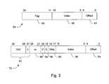
- FIG. 3a block diagram illustrating an exemplary memory transaction address 50 and an exemplary direct access transaction address 52 is shown.
- the addresses illustrated in FIG. 3may correspond to the embodiment illustrated in FIG. 2 .
- Memory transaction address 50includes an offset field 54 , an index field 56 , and a tag field 58 .
- Offset field 54includes the bits defining the offset within a cache line.
- Index field 56includes the bits used to index L2 cache 14 (e.g. bits 16 : 5 in the embodiment illustrated in FIG. 2 ).
- Tag field 58includes the remaining bits of the address not included in offset field 54 and index field 56 .
- Tag field 58includes the address bits stored in tag memory 30 and compared to the corresponding portion of the input address.
- Direct access transaction address 52includes offset field 54 and index field 56 , similar to memory transaction address 50 . Additionally, direct access transaction address 52 includes a way field 60 identifying the way to be accessed in response to the direct access transaction (e.g. bits 18 : 17 in the embodiment illustrated in FIG. 2 ). A field 62 including a set of most significant bits of direct access transaction address 52 are encoded to select the direct access memory address space (e.g. bits 39 : 27 in the embodiment illustrated in FIG. 2 ). Any encoding may be used to identify the direct access address space according to design choice. Direct access transaction address 52 further includes a valid bit 64 and a dirty bit 66 . These bits may be written to the valid and dirty bits of the selected tag entry if a tag update is performed (e.g.
- bits comprising offset field 54may not actually be transmitted on one embodiment of bus 24 . Instead, byte enables may be transmitted indicating which bytes are accessed by the transaction. The byte enable for the byte identified by offset field 54 is set, and additional byte enables based on the size of the transaction may be set.
- FIG. 4a flowchart illustrating operation of one embodiment of L2 cache 14 (and more particularly control circuit 36 and/or replacement circuit 44 , in the embodiment of FIG. 2) for a read transaction is shown.
- Other embodimentsare possible and contemplated. While the blocks shown in FIG. 4 may be illustrated in a particular order for ease of understanding, the blocks may be performed in parallel by combinatorial logic circuitry within L2 cache 14 . Furthermore, various blocks may be performed in different clock cycles (e.g. the operation may be pipelined) according to design choice.
- L2 cache 14provides the data from the selected entry in response to the read transaction (block 72 ).
- the selected entryis identified by the explicit index and way provided by the direct access transaction. Whether or not the tag portion of the address in the selected entry matches the address of the read transaction does not affect the forwarding of data, and no cache eviction may occur.
- replacement circuit 44may establish a state corresponding to the specified way in response to the direct access transaction (block 73 ).
- the state establishedmay result in an eviction from the specified way if the next transaction is a miss in L2 cache 14 .
- L2 cache 14determines if the address hits (decision block 74 ). If the address hits, the data from the hitting entry is provided in response to the read transaction (block 76 ). If the read transaction is a miss, L2 cache 14 selects an entry for eviction of the cache line stored therein, to be replaced by the cache line accessed by the read transaction (block 78 ).
- FIG. 5a flowchart illustrating operation of one embodiment of L2 cache 14 (and more particularly control circuit 36 and/or replacement circuit 44 , in the embodiment of FIG. 2) for a write transaction is shown.
- Other embodimentsare possible and contemplated. While the blocks shown in FIG. 5 may be illustrated in a particular order for ease of understanding, the blocks may be performed in parallel by combinatorial logic circuitry within L2 cache 14 . Furthermore, various blocks may be performed in different clock cycles (e.g. the operation may be pipelined) according to design choice.
- L2 cache 14stores the data included in the write transaction into the selected entry (block 82 ).
- the selected entryis identified by the explicit index and way provided by the direct access transaction. Whether or not the tag portion of the address in the selected entry matches the address of the write transaction does not affect the updating of the selected entry. Furthermore, if valid data is stored in the entry, that data is overwritten (even if the tag does not match the address of the write transaction). Additionally, the tag of the selected entry may be updated with the corresponding portion of the address of the write transaction (block 84 ). In this manner, the entry may not be affected by coherency activity in the memory address space.
- replacement circuit 44may establish a state corresponding to the specified way in response to the direct access transaction (block 85 ).
- the state establishedmay result in an eviction from the specified way if the next transaction is a miss in L2 cache 14 .
- L2 cache 14determines if the address hits (decision block 86 ). If the address hits, the data included in the write transaction is written to the hitting entry (block 88 ). If the write transaction is a miss, L2 cache 14 selects an entry for eviction of the cache line stored therein, to be replaced by the cache line accessed by the write transaction (block 90 ).
- FIG. 5allocates an entry for write memory transactions which miss L2 cache 14
- other embodimentsmay not allocate an entry for write misses or may provide for programmability of write allocation, as desired.
- the embodiment illustrated via FIGS. 4 and 5assumes that the transaction is cacheable in L2 cache 14 . Some embodiments may provide for indicating the cacheability of each transaction. If a transaction is indicated to be non-cacheable, L2 cache 14 may not respond to the transaction.
- replacement circuit 44includes a control circuit 100 , a register 102 , an output circuit 104 , and a next state circuit 106 .
- Control circuit 100is coupled to receive the direct access signal from decoder 38 , the portion of the input address specifying the way for direct access transactions, and an access signal from control circuit 36 .
- Control circuit 100is coupled to provide control signals and an override value to register 102 , which is coupled to output circuit 104 and next state circuit 106 .
- Output circuit 104is coupled to provide a replacement way to control circuit 36 .
- replacement circuit 44provides a replacement way to control circuit 36 for use in evicting a cache line if a miss is detected.
- Register 102stores a state of replacement circuit 36
- output circuit 104generates the replacement way from the state. More particularly, output circuit 104 may logically combine various bits from register 102 to generate the replacement way.
- the logic gates and bits combined by the logic gates as illustrated in output circuit 104are merely exemplary. Any bits may be combined in any logic equation to generate the replacement way.
- replacement circuit 44changes state for each access of L2 cache 14 (irrespective of whether or not the access hits or misses).
- control circuit 36signals replacement circuit 44 if an access is received by L2 cache 14 via the access signal.
- Control circuit 100may cause register 102 to capture a new state in response to the access signal. More particularly, register 102 may be a linear feedback shift register.
- Next state circuit 106may generate a bit to be shifted into register 102 , and the remaining bits may be shifted to the right (as illustrated in FIG. 6 ), with the rightmost bit being deleted from register 102 .
- Control circuit 100may assert a shift control signal to register 102 , causing register 102 to shift in the bit from next state circuit 106 and shift the remaining bits.
- next state circuit 106The logic gate and bits combined by the logic gate as illustrated in next state circuit 106 are merely exemplary. Any bits may be combined in any logic equation to generate the next state. Generally, the combination of output circuit 104 and next state circuit 106 may be selected so that the distribution of ways selected over time has reasonable dispersion (e.g. the pattern of ways selected over consecutive state changes tends not to select the same way consecutively and repeatedly).
- control circuit 100overrides the value in register 102 with a predetermined value.
- the predetermined valuerepresents a state in register 102 which generates a particular way as the replacement way to control circuit 36 .
- the particular wayis the way indicated by the direct access transaction, which is received by control circuit 100 .
- control circuit 100may select the predetermined value from one of a set of predetermined values (one for each way of L2 cache 14 ).
- the predetermined valueis provided to register 102 (override[ 7 : 0 ] in FIG. 6 ), and control circuit 100 asserts a control signal to register 102 causing register 102 to update with the predetermined value.
- register 102may be an eight bit register. However, any number of bits may be used in other embodiments.
- table 1 belowprovides an example of predetermined values that may be used by control circuit 100 to establish a state in register 102 which causes the way identified by a direct access transaction to be the way used for a succeeding miss. The values are shown in binary, with bit 0 being the rightmost bit of register 102 as shown in FIG. 6 and bit 7 being the leftmost bit of register 102 . Don't care bits are shown as an “x” and may be zero or one (or may be left at the state currently in register 102 ). Any other predetermined values which generate the desired replacement way for the circuitry shown in FIG. 6 may be used as well.
- register 102may be a linear feedback shift register.
- registers 102may employ other registers.
- a countercould be used to count through the possible ways, rather than the linear feedback shift register.
- register 102may be memory mapped, and a memory mapped write to register 102 may set the state.
- the memory mapped writemay provide the desired way, and the corresponding state may be set.
- a dedicated bus commandmay be used to convey the state or desired way.
- an “associative cache”may be any type of cache in which two or more entries are eligible to store data corresponding to a given address.
- An associative cachemay include both set associative and fully associative caches.
- FIG. 7a flowchart is shown illustrating operation of one embodiment of control circuit 100 .
- Other embodimentsare possible and contemplated. While the blocks shown in FIG. 7 may be illustrated in a particular order for ease of understanding, the blocks may be performed in parallel by combinatorial logic circuitry within control circuit 100 .
- control circuit 100may override the state of replacement circuit 44 with a predetermined value corresponding to the way specified by the direct access transaction (block 112 ). On the other hand, if a memory access is received (decision block 114 ), control circuit 100 may cause register 102 to change to the next random state (e.g. to shift in the bit from next state circuit 106 and right shift the other bits—block 116 ).
- FIG. 8a flowchart is shown illustrating an exemplary sequence of transactions which may be performed to achieve a test of an entry in the L2 cache memory.
- the sequence of transactionscould be generated, e.g., by a processor 12 A- 12 B executing a code sequence which includes instructions which result in the transactions. Additionally illustrated in FIG. 8 are certain checks, which could be performed by other instructions than those resulting in the transactions. Alternatively, the sequence of transactions and checks could be performed by any other device connected to bus 24 .
- a first direct access transactionis performed to select a test way (block 120 ). More particularly, the replacement circuit in L2 cache 14 may establish the test way as the way to be selected for eviction if the next transaction is a miss in response to the first direct access transaction.
- the first direct access transactionmay be a read or a write.
- a memory transactionmay be performed (block 122 ).
- the memory transactionmay be a read or a write, and reads the desired test data from memory 26 or writes the desired test data to memory 26 .
- the memory transactionshould be a miss in L2 cache 14 , so that L2 cache 14 allocates an entry for the cache line and stores the test data. More particularly, since the first direct access transaction established the test way as the way to be selected for eviction, the entry allocated to the test data is in the test way.
- the index from the memory transaction addressselects the set of entries from which the entry is allocated. Thus, the entry is written with the test data has been directly selected via the first direct access transaction and the memory transaction, and the desired test data has been written to the selected entry.
- a direct access read transactionis performed (block 124 ).
- the direct access read transactionexplicitly specifies the entry written with the test data (e.g. by index and way). Accordingly, the data returned for the direct access read transaction should be the test data, if no error occurred in storing the data in the entry.
- the read data returned in response to the direct access read transactionis compared to the test data (decision block 126 ). If the read data does not match the test data, then the test fails (block 128 ).
- the L2 cache entryincludes storage for tag information.
- the tagis updated with the address of the memory transaction from block 122 .
- L2 cache 14stores the tag of the entry in tag register 42 .
- the testmay include a read of tag register 42 (block 130 ).
- the tag information received in response to the read of the tag register 42may be compared to corresponding information from the address used in the memory transaction (decision block 132 ) and expected values for the other information (e.g. valid, dirty, ECC, etc.). If the tag information does not match, then the test fails (block 128 ). If the tag information does match, then the test passes (block 134 ).
- the above sequence of transactions and checkstests one entry of L2 cache 14 .
- Other entriesmay be tested by repeating the above sequence for each index and each way within each index.
- the transactions for each entrymay be interleaved with the transactions for other entries, to investigate the possibility of cross coupling between entries. Additionally, the transactions may be repeated for each desired test data pattern or test tag pattern, to allow for robust testing of the memory.
- While the above transactionsinclude a first direct access transaction to set the test way, a memory transaction to store the test data in the selected entry, and a direct access read transaction to read the data for validation, an alternative is contemplated.
- a direct access write transactionis used to store the test data and a direct access read transaction is used to read the test data for comparison.
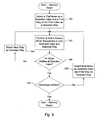
- FIG. 9a flowchart is shown illustrating an exemplary sequence of transactions which may be performed to achieve a reset of the L2 cache memory.
- the sequence of transactionscould be generated, e.g., by a processor 12 A- 12 B executing a code sequence which includes instructions which result in the transactions.
- the sequence of transactions and checkscould be performed by any other device connected to bus 24 .
- a first indexis selected as the selected index and a first way is selected as the selected way (block 140 ).
- index zero and way zeromay be selected as the selected index and selected way.
- a direct access write transactionis performed to the selected index and the selected way (block 142 ).
- the data for the direct access write transactionmay be any data, and the data is written to the entry corresponding to the selected index and the selected way.
- the valid indication carried by the address of the direct access write transactionmay be set to zero to indicate that the cache line in the entry is invalid. However, the data is set to a known state. Since evictions are not performed for direct access transactions, the data formerly stored in the entry is overwritten without causing an eviction. Additionally, for embodiments employing ECC protection, correct ECC data is written so no ECC errors should occur after the L2 cache is reset.
- Block 142is then repeated for the selected index and selected way. Once all ways at the selected index have been written, unless all indexes have been processed (decision block 148 ), the next index is selected as the selected index and the first way is selected as the selected way (block 150 ). Block 142 is then repeated for the selected index and the selected way.
- block 142is repeated for each index and each way within each index.
- the order of traversal(first all the ways of the index and then moving to the next index versus all the indexes in one way and then moving to the next way) is unimportant and may be varied as desired.
- L2 cache 14has been reset and all entries are storing information of a known state. Thus, ensuring that the L2 cache memory resets to a known state in hardware may not be required. Instead, direct access transactions may be used to perform the reset.
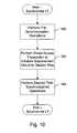
- FIG. 10a flowchart is shown illustrating an exemplary sequence of transactions which may be performed to synchronize the L2 cache (particularly the pseudo-random replacement algorithm).
- the sequence of transactionscould be generated, e.g., by a processor 12 A- 12 B executing a code sequence which includes instructions which result in the transactions.
- the sequence of transactions and checkscould be performed by any other device connected to bus 24 .
- the sequencemay include one or more “pre-synchronization” operations (block 160 ).
- a direct access transactionmay be performed to initialize the replacement circuit to a desired way explicitly specified by the direct access transaction (block 162 ).
- the direct access transactionmay be either a read or a write, as desired.
- one or more “post-synchronization” operationsmay be performed (block 164 ).
- Synchronizing the L2 cache replacement policy using the deterministic setting provided in response to direct access transactionsmay have a variety of uses. For example, it may be desirable to run validation tests used to test the L2 cache or other system components in a variety of test environments (e.g. simulation of the VHDL code representing the system 10 , emulation in which the system 10 is implemented in programmable logic devices for test purposes, a test board validation environment with the manufactured component or components, and/or a system validation environment with the manufactured component or components).
- the mechanisms used to establish an initial state in these various environmentsmay differ, and thus the state of the L2 replacement circuit may differ when the test itself is to be started. Having a different state in the replacement circuit may affect the operation of the test, and thus the same validation may not occur.
- the same state in the replacement circuitmay be established. Additionally, if a particular entry is desired to store data corresponding to a particular transaction within a test, that entry can be selected using a direct access transaction prior to the particular transaction.
- FIG. 11a flowchart is shown illustrating an exemplary sequence of transactions which may be performed to flush the L2 cache without requiring an explicit flush command on bus 24 . More particularly, the sequence shown in FIG. 11 may be used to flush every entry of the L2 cache. An entry is flushed if the cache line stored in the entry is invalidated, and the cache line is written to memory 26 if dirty. Other embodiments are possible and contemplated.
- the sequence of transactionscould be generated, e.g., by a processor 12 A- 12 B executing a code sequence which includes instructions which result in the transactions. Alternatively, the sequence of transactions and checks could be performed by any other device connected to bus 24 .
- a first indexis selected as the selected index and a first way is selected as the selected way (block 170 ).
- index zero and way zeromay be selected as the selected index and selected way.
- a direct access read transactionis performed to the selected index and selected way (block 172 ).
- replacement circuit 44establishes a state indicating that the selected way is to be selected for eviction for the next transaction.
- L2 cache 14After the direct access read transaction, a memory transaction which misses the L2 cache is performed to the selected index (block 174 ). Since the memory transaction misses, L2 cache 14 allocates an entry for the affected cache line. The entry is allocated from the selected way, evicting the cache line in the selected way.
- Blocks 176 , 178 , 180 , and 182illustrate the repeating of blocks 172 and 174 for each entry in the L2 cache, similar to blocks 144 , 146 , 148 and 150 shown in FIG. 9 . Again, the order of traversal may be any suitable order. After repeating blocks 172 and 174 for each entry, the prior contents of the L2 cache have been flushed, and no explicit flush command was used. Having an explicit flush command may require additional hardware in L2 cache 14 , and may occupy a command code point on bus 24 , and thus may be undesirable.
- FIG. 12a flowchart is shown illustrating an exemplary sequence of transactions which may be performed to flush a particular cache line from the L2 cache without requiring an explicit flush command on bus 24 .
- the sequence of transactionscould be generated, e.g., by a processor 12 A- 12 B executing a code sequence which includes instructions which result in the transactions.
- the sequence of transactions and checkscould be performed by any other device connected to bus 24 .
- the address of the cache lineis known.
- the index of the desired cache linemay be selected as the selected index and the first way of the index may be selected as the selected way (block 190 ).
- a direct access read transactionis performed to the selected index and the selected way (block 192 ).
- the replacement circuit 44establishes a state indicating that the selected way is to be selected for eviction for the next transaction. Additionally, the tag of the entry explicitly identified (by the selected index and selected way) is stored into tag register 42 .
- a read transactionmay subsequently be performed to the tag register 42 to retrieve the tag information corresponding to the entry identified by the above direct access read transaction (block 194 ). Since the read transaction is not a direct access transaction nor an access to the cache memory, the replacement policy may be unaffected by the read transaction.
- a transaction to the selected index which misses L2 cache 14may be performed (block 198 ). Since the transaction misses, an eviction occurs and, due to the setting of the replacement policy via the direct access read transaction, the way storing the desired cache line is the way selected for eviction. Thus, the desired cache line is flushed from L2 cache 14 .
- FIGS. 8-12have illustrated various uses for the direct access transactions and/or the deterministic setting of the replacement policy, these features of the cache may be used for a variety of uses. Furthermore, any cache may employ these features.
- a carrier medium 300 including a database representative of system 10may include storage media such as magnetic or optical media, e.g., disk or CD-ROM, volatile or non-volatile memory media such as RAM (e.g. SDRAM, RDRAM, SRAM, etc.), ROM, etc., as well as transmission media or signals such as electrical, electromagnetic, or digital signals, conveyed via a communication medium such as a network and/or a wireless link.
- storage mediasuch as magnetic or optical media, e.g., disk or CD-ROM, volatile or non-volatile memory media such as RAM (e.g. SDRAM, RDRAM, SRAM, etc.), ROM, etc.
- RAMe.g. SDRAM, RDRAM, SRAM, etc.
- ROMetc.
- transmission media or signalssuch as electrical, electromagnetic, or digital signals
- the database of system 10 carried on carrier medium 300may be a database which can be read by a program and used, directly or indirectly, to fabricate the hardware comprising system 10 .
- the databasemay be a behavioral-level description or register-transfer level (RTL) description of the hardware functionality in a high level design language (HDL) such as Verilog or VHDL.
- the descriptionmay be read by a synthesis tool which may synthesize the description to produce a netlist comprising a list of gates in a synthesis library.
- the netlistcomprises a set of gates which also represent the functionality of the hardware comprising system 10 .
- the netlistmay then be placed and routed to produce a data set describing geometric shapes to be applied to masks.
- the masksmay then be used in various semiconductor fabrication steps to produce a semiconductor circuit or circuits corresponding to system 10 .
- the database on carrier medium 300may be the netlist (with or without the synthesis library) or the data set, as desired.
- carrier medium 300carries a representation of system 10
- other embodimentsmay carry a representation of any portion of system 10 , as desired, including any set of one or more agents (e.g. processors, L2 cache, memory controller, etc.) or circuitry therein (e.g. replacement circuits, caches, tags, etc.), etc.
- agentse.g. processors, L2 cache, memory controller, etc.
- circuitry thereine.g. replacement circuits, caches, tags, etc.
Landscapes
- Engineering & Computer Science (AREA)
- Theoretical Computer Science (AREA)
- Physics & Mathematics (AREA)
- General Engineering & Computer Science (AREA)
- General Physics & Mathematics (AREA)
- Memory System Of A Hierarchy Structure (AREA)
Abstract
Description
| TABLE 1 |
| Exemplary Values for Loading into Register |
| Direct Access Way | Override[7:0] | ||
| 0 | |||
| 1 | x1x00000 | ||
| 2 | x0x10000 | ||
| 3 | x0x00000 | ||
Claims (40)
Priority Applications (3)
| Application Number | Priority Date | Filing Date | Title |
|---|---|---|---|
| US09/633,544US6732234B1 (en) | 2000-08-07 | 2000-08-07 | Direct access mode for a cache |
| EP01306709AEP1179779A3 (en) | 2000-08-07 | 2001-08-06 | Direct access mode for a cache |
| US10/748,551US7177986B2 (en) | 2000-08-07 | 2003-12-30 | Direct access mode for a cache |
Applications Claiming Priority (1)
| Application Number | Priority Date | Filing Date | Title |
|---|---|---|---|
| US09/633,544US6732234B1 (en) | 2000-08-07 | 2000-08-07 | Direct access mode for a cache |
Related Child Applications (1)
| Application Number | Title | Priority Date | Filing Date |
|---|---|---|---|
| US10/748,551ContinuationUS7177986B2 (en) | 2000-08-07 | 2003-12-30 | Direct access mode for a cache |
Publications (1)
| Publication Number | Publication Date |
|---|---|
| US6732234B1true US6732234B1 (en) | 2004-05-04 |
Family
ID=24540058
Family Applications (2)
| Application Number | Title | Priority Date | Filing Date |
|---|---|---|---|
| US09/633,544Expired - Fee RelatedUS6732234B1 (en) | 2000-08-07 | 2000-08-07 | Direct access mode for a cache |
| US10/748,551Expired - Fee RelatedUS7177986B2 (en) | 2000-08-07 | 2003-12-30 | Direct access mode for a cache |
Family Applications After (1)
| Application Number | Title | Priority Date | Filing Date |
|---|---|---|---|
| US10/748,551Expired - Fee RelatedUS7177986B2 (en) | 2000-08-07 | 2003-12-30 | Direct access mode for a cache |
Country Status (2)
| Country | Link |
|---|---|
| US (2) | US6732234B1 (en) |
| EP (1) | EP1179779A3 (en) |
Cited By (13)
| Publication number | Priority date | Publication date | Assignee | Title |
|---|---|---|---|---|
| US20020116501A1 (en)* | 2001-02-21 | 2002-08-22 | Ho Chi Fai | Service tunnel over a connectionless network |
| US20030051197A1 (en)* | 2001-06-20 | 2003-03-13 | Broadcom Corporation | Cache memory self test |
| US20040168031A1 (en)* | 2003-02-21 | 2004-08-26 | Gregory Haskins | Methods for improved data caching |
| US20060004962A1 (en)* | 2004-07-02 | 2006-01-05 | Shawn Walker | Cache memory system and method capable of adaptively accommodating various memory line sizes |
| US20060036840A1 (en)* | 2001-10-30 | 2006-02-16 | Microsoft Corporation | Network interface sharing methods and apparatuses that support kernel mode data traffic and user mode data traffic |
| US20070002482A1 (en)* | 2005-06-30 | 2007-01-04 | Fujitsu Limited | Storage system, storage control device, and storage control method |
| US20080209131A1 (en)* | 2006-11-22 | 2008-08-28 | Kornegay Marcus L | Structures, systems and arrangements for cache management |
| US20080244111A1 (en)* | 2007-04-02 | 2008-10-02 | Naoto Tobita | Information Processing Terminal, Data Transfer Method, and Program |
| US20110010504A1 (en)* | 2009-07-10 | 2011-01-13 | James Wang | Combined Transparent/Non-Transparent Cache |
| US20110010520A1 (en)* | 2009-07-10 | 2011-01-13 | James Wang | Block-Based Non-Transparent Cache |
| US20150170764A1 (en)* | 2013-12-13 | 2015-06-18 | International Business Machines Corporation | Detecting missing write to cache/memory operations |
| US10120809B2 (en) | 2015-09-26 | 2018-11-06 | Intel Corporation | Method, apparatus, and system for allocating cache using traffic class |
| US11086777B2 (en)* | 2019-04-01 | 2021-08-10 | Arm Limited | Replacement of cache entries in a set-associative cache |
Families Citing this family (17)
| Publication number | Priority date | Publication date | Assignee | Title |
|---|---|---|---|---|
| EP1361518B1 (en)* | 2002-05-10 | 2013-08-07 | Texas Instruments Incorporated | Reducing TAG-RAM accesses and accelerating cache operation during cache miss |
| JP4443200B2 (en)* | 2003-12-01 | 2010-03-31 | 富士通株式会社 | Information system |
| US7237067B2 (en)* | 2004-04-22 | 2007-06-26 | Hewlett-Packard Development Company, L.P. | Managing a multi-way associative cache |
| US7707463B2 (en)* | 2005-11-30 | 2010-04-27 | International Business Machines Corporation | Implementing directory organization to selectively optimize performance or reliability |
| US7594145B2 (en)* | 2006-05-31 | 2009-09-22 | Fujitsu Limited | Improving performance of a processor having a defective cache |
| US7805658B2 (en)* | 2007-02-12 | 2010-09-28 | International Business Machines Corporation | DRAM Cache with on-demand reload |
| GB2451668A (en)* | 2007-08-08 | 2009-02-11 | Advanced Risc Mach Ltd | Error correction in a set associative cache |
| US20100061207A1 (en)* | 2008-09-09 | 2010-03-11 | Seagate Technology Llc | Data storage device including self-test features |
| US8364896B2 (en)* | 2008-09-20 | 2013-01-29 | Freescale Semiconductor, Inc. | Method and apparatus for configuring a unified cache based on an associated error rate |
| US8316186B2 (en)* | 2008-09-20 | 2012-11-20 | Freescale Semiconductor, Inc. | Method and apparatus for managing cache reliability based on an associated error rate |
| US8504777B2 (en)* | 2010-09-21 | 2013-08-06 | Freescale Semiconductor, Inc. | Data processor for processing decorated instructions with cache bypass |
| US8352646B2 (en) | 2010-12-16 | 2013-01-08 | International Business Machines Corporation | Direct access to cache memory |
| US9189424B2 (en)* | 2011-05-31 | 2015-11-17 | Hewlett-Packard Development Company, L.P. | External cache operation based on clean castout messages |
| SG190505A1 (en)* | 2011-11-24 | 2013-06-28 | Chikka Pte Ltd | System and method for detecting broadband service and a charging mechanism for same |
| US9058282B2 (en) | 2012-12-31 | 2015-06-16 | Intel Corporation | Dynamic cache write policy |
| US9965391B2 (en) | 2014-06-30 | 2018-05-08 | Hewlett Packard Enterprise Development Lp | Access cache line from lower level cache |
| US9507628B1 (en) | 2015-09-28 | 2016-11-29 | International Business Machines Corporation | Memory access request for a memory protocol |
Citations (86)
| Publication number | Priority date | Publication date | Assignee | Title |
|---|---|---|---|---|
| US3693165A (en) | 1971-06-29 | 1972-09-19 | Ibm | Parallel addressing of a storage hierarchy in a data processing system using virtual addressing |
| US4044338A (en) | 1975-02-10 | 1977-08-23 | Siemens Aktiengesellschaft | Associative memory having separately associable zones |
| EP0061570A2 (en) | 1981-03-23 | 1982-10-06 | International Business Machines Corporation | Store-in-cache multiprocessor system with checkpoint feature |
| US4453212A (en) | 1981-07-13 | 1984-06-05 | Burroughs Corporation | Extended address generating apparatus and method |
| US4511994A (en) | 1982-09-27 | 1985-04-16 | Control Data Corporation | Multi-group LRU resolver |
| US4575792A (en)* | 1982-03-31 | 1986-03-11 | Honeywell Information Systems Inc. | Shared interface apparatus for testing the memory sections of a cache unit |
| US4633440A (en) | 1984-12-31 | 1986-12-30 | International Business Machines | Multi-port memory chip in a hierarchical memory |
| US4654778A (en) | 1984-06-27 | 1987-03-31 | International Business Machines Corporation | Direct parallel path for storage accesses unloading common system path |
| EP0259095A2 (en) | 1986-08-27 | 1988-03-09 | Amdahl Corporation | Cache storage queue |
| US4807115A (en) | 1983-10-07 | 1989-02-21 | Cornell Research Foundation, Inc. | Instruction issuing mechanism for processors with multiple functional units |
| US4833642A (en) | 1987-03-31 | 1989-05-23 | Nec Corporation | Cache controller giving versatility to cache memory structure |
| EP0325420A2 (en) | 1988-01-20 | 1989-07-26 | Advanced Micro Devices, Inc. | Organization of an integrated cache unit for flexible usage in cache system design |
| US4858105A (en) | 1986-03-26 | 1989-08-15 | Hitachi, Ltd. | Pipelined data processor capable of decoding and executing plural instructions in parallel |
| GB2214336A (en) | 1988-01-21 | 1989-08-31 | Mitsubishi Electric Corp | Cache memory apparatus |
| US4907278A (en) | 1987-06-25 | 1990-03-06 | Presidenza Dei Consiglio Dei Ministri Del Ministro Per Il Coordinamento Delle Iniziative Per La Ricerca Scientifica E Tecnologica, Dello Stato Italiano | Integrated processing unit, particularly for connected speech recognition systems |
| EP0381471A2 (en) | 1989-02-03 | 1990-08-08 | Digital Equipment Corporation | Method and apparatus for preprocessing multiple instructions in a pipeline processor |
| US4996641A (en)* | 1988-04-15 | 1991-02-26 | Motorola, Inc. | Diagnostic mode for a cache |
| EP0436092A2 (en) | 1989-12-26 | 1991-07-10 | International Business Machines Corporation | Out-of-sequence fetch controls for a data processing system |
| EP0459233A2 (en) | 1990-05-29 | 1991-12-04 | National Semiconductor Corporation | Selectively locking memory locations within a microprocessor's on-chip cache |
| EP0459232A2 (en) | 1990-05-29 | 1991-12-04 | National Semiconductor Corporation | Partially decoded instruction cache |
| US5125083A (en) | 1989-02-03 | 1992-06-23 | Digital Equipment Corporation | Method and apparatus for resolving a variable number of potential memory access conflicts in a pipelined computer system |
| US5163142A (en) | 1988-10-28 | 1992-11-10 | Hewlett-Packard Company | Efficient cache write technique through deferred tag modification |
| US5193163A (en)* | 1990-10-01 | 1993-03-09 | Digital Equipment Corporation | Two-level protocol for multi-component bus ownership, and implementation in a multi-processor cache write back protocol |
| US5226130A (en) | 1990-02-26 | 1993-07-06 | Nexgen Microsystems | Method and apparatus for store-into-instruction-stream detection and maintaining branch prediction cache consistency |
| US5226126A (en) | 1989-02-24 | 1993-07-06 | Nexgen Microsystems | Processor having plurality of functional units for orderly retiring outstanding operations based upon its associated tags |
| GB2263985A (en) | 1992-02-06 | 1993-08-11 | Intel Corp | Deriving variable length instructions from a stream of instructions |
| GB2263987A (en) | 1992-02-06 | 1993-08-11 | Intel Corp | End bit markers for instruction decode. |
| US5241663A (en) | 1990-05-31 | 1993-08-31 | Sony Corporation | Hierarchically pairing memory blocks based upon relative storage capacities and simultaneously accessing each memory block within the paired memory blocks |
| EP0568221A1 (en) | 1992-04-29 | 1993-11-03 | Sun Microsystems, Inc. | Methods and apparatus for implementing a pseudo-LRU cache memory replacement scheme with a locking feature |
| US5317716A (en) | 1988-08-16 | 1994-05-31 | International Business Machines Corporation | Multiple caches using state information indicating if cache line was previously modified and type of access rights granted to assign access rights to cache line |
| US5325504A (en) | 1991-08-30 | 1994-06-28 | Compaq Computer Corporation | Method and apparatus for incorporating cache line replacement and cache write policy information into tag directories in a cache system |
| US5369753A (en) | 1990-06-15 | 1994-11-29 | Compaq Computer Corporation | Method and apparatus for achieving multilevel inclusion in multilevel cache hierarchies |
| US5377345A (en) | 1992-04-29 | 1994-12-27 | Sun Microsystems, Inc. | Methods and apparatus for providing multiple pending operations in a cache consistent multiple processor computer system |
| GB2281422A (en) | 1993-08-26 | 1995-03-01 | Intel Corp | Processor ordering consistency for a processor performing out-of-order instruction execution |
| US5416783A (en) | 1993-08-09 | 1995-05-16 | Motorola, Inc. | Method and apparatus for generating pseudorandom numbers or for performing data compression in a data processor |
| US5432918A (en) | 1990-06-29 | 1995-07-11 | Digital Equipment Corporation | Method and apparatus for ordering read and write operations using conflict bits in a write queue |
| US5450551A (en) | 1993-05-28 | 1995-09-12 | International Business Machines Corporation | System direct memory access (DMA) support logic for PCI based computer system |
| US5471598A (en) | 1993-10-18 | 1995-11-28 | Cyrix Corporation | Data dependency detection and handling in a microprocessor with write buffer |
| EP0687979A1 (en) | 1994-06-14 | 1995-12-20 | Kabushiki Kaisha Toshiba | Cache memory having lockable entries |
| US5487162A (en) | 1992-02-25 | 1996-01-23 | Matsushita Electric Industrial Co., Ltd. | Cache lock information feeding system using an address translator |
| US5493667A (en) | 1993-02-09 | 1996-02-20 | Intel Corporation | Apparatus and method for an instruction cache locking scheme |
| US5510934A (en) | 1993-12-15 | 1996-04-23 | Silicon Graphics, Inc. | Memory system including local and global caches for storing floating point and integer data |
| US5524208A (en)* | 1994-06-09 | 1996-06-04 | Dell Usa, L.P. | Method and apparatus for performing cache snoop testing using DMA cycles in a computer system |
| US5526510A (en) | 1994-02-28 | 1996-06-11 | Intel Corporation | Method and apparatus for implementing a single clock cycle line replacement in a data cache unit |
| US5539878A (en)* | 1995-06-16 | 1996-07-23 | Elonex Technologies, Inc. | Parallel testing of CPU cache and instruction units |
| US5551001A (en) | 1994-06-29 | 1996-08-27 | Exponential Technology, Inc. | Master-slave cache system for instruction and data cache memories |
| US5557763A (en) | 1992-09-29 | 1996-09-17 | Seiko Epson Corporation | System for handling load and/or store operations in a superscalar microprocessor |
| US5564034A (en) | 1992-09-24 | 1996-10-08 | Matsushita Electric Industrial Co., Ltd. | Cache memory with a write buffer indicating way selection |
| US5584014A (en) | 1994-12-20 | 1996-12-10 | Sun Microsystems, Inc. | Apparatus and method to preserve data in a set associative memory device |
| US5586293A (en) | 1991-08-24 | 1996-12-17 | Motorola, Inc. | Real time cache implemented by on-chip memory having standard and cache operating modes |
| US5586253A (en)* | 1994-12-15 | 1996-12-17 | Stratus Computer | Method and apparatus for validating I/O addresses in a fault-tolerant computer system |
| US5588126A (en) | 1993-12-30 | 1996-12-24 | Intel Corporation | Methods and apparatus for fordwarding buffered store data on an out-of-order execution computer system |
| US5592679A (en) | 1994-11-14 | 1997-01-07 | Sun Microsystems, Inc. | Apparatus and method for distributed control in a processor architecture |
| US5638537A (en) | 1993-01-29 | 1997-06-10 | Mitsubishi Denki Kabushiki Kaisha | Cache system with access mode determination for prioritizing accesses to cache memory |
| US5644752A (en) | 1994-06-29 | 1997-07-01 | Exponential Technology, Inc. | Combined store queue for a master-slave cache system |
| US5668815A (en) | 1996-08-14 | 1997-09-16 | Advanced Micro Devices, Inc. | Method for testing integrated memory using an integrated DMA controller |
| US5668972A (en) | 1994-10-05 | 1997-09-16 | International Business Machines Corporation | Method and system for efficient miss sequence cache line allocation utilizing an allocation control cell state to enable a selected match line |
| US5671444A (en) | 1994-02-28 | 1997-09-23 | Intel Corporaiton | Methods and apparatus for caching data in a non-blocking manner using a plurality of fill buffers |
| US5748640A (en) | 1996-09-12 | 1998-05-05 | Advanced Micro Devices | Technique for incorporating a built-in self-test (BIST) of a DRAM block with existing functional test vectors for a microprocessor |
| US5752261A (en)* | 1996-11-07 | 1998-05-12 | Ncr Corporation | Method and apparatus for detecting thrashing in a cache memory |
| US5761712A (en) | 1995-06-07 | 1998-06-02 | Advanced Micro Devices | Data memory unit and method for storing data into a lockable cache in one clock cycle by previewing the tag array |
| US5768555A (en) | 1997-02-20 | 1998-06-16 | Advanced Micro Devices, Inc. | Reorder buffer employing last in buffer and last in line bits |
| US5784588A (en) | 1997-06-20 | 1998-07-21 | Sun Microsystems, Inc. | Dependency checking apparatus employing a scoreboard for a pair of register sets having different precisions |
| US5787490A (en)* | 1995-10-06 | 1998-07-28 | Fujitsu Limited | Multiprocess execution system that designates cache use priority based on process priority |
| US5802338A (en) | 1996-10-01 | 1998-09-01 | International Business Machines Corporation | Method of self-parallelizing and self-parallelizing multiprocessor using the method |
| US5809528A (en) | 1996-12-24 | 1998-09-15 | International Business Machines Corporation | Method and circuit for a least recently used replacement mechanism and invalidated address handling in a fully associative many-way cache memory |
| US5809531A (en) | 1992-09-21 | 1998-09-15 | Intel Corporation | Computer system for executing programs using an internal cache without accessing external RAM |
| US5875465A (en) | 1996-04-03 | 1999-02-23 | Arm Limited | Cache control circuit having a pseudo random address generator |
| US5913224A (en) | 1997-02-26 | 1999-06-15 | Advanced Micro Devices, Inc. | Programmable cache including a non-lockable data way and a lockable data way configured to lock real-time data |
| US5974507A (en) | 1997-04-14 | 1999-10-26 | International Business Machines Corporation | Optimizing a cache eviction mechanism by selectively introducing different levels of randomness into a replacement algorithm |
| US5983321A (en) | 1997-03-12 | 1999-11-09 | Advanced Micro Devices, Inc. | Cache holding register for receiving instruction packets and for providing the instruction packets to a predecode unit and instruction cache |
| EP0997821A1 (en) | 1998-10-30 | 2000-05-03 | Nec Corporation | Cache memory having a freeze function |
| US6115792A (en)* | 1997-12-16 | 2000-09-05 | Advanced Micro Devices, Inc. | Way prediction logic for cache array |
| US6148370A (en)* | 1996-06-05 | 2000-11-14 | Kabushiki Kaisha Toshiba | Semiconductor memory device including cache memory used as a RAM |
| US6161167A (en) | 1997-06-27 | 2000-12-12 | Advanced Micro Devices, Inc. | Fully associate cache employing LRU groups for cache replacement and mechanism for selecting an LRU group |
| US6185657B1 (en) | 1998-04-20 | 2001-02-06 | Motorola Inc. | Multi-way cache apparatus and method |
| US6185703B1 (en)* | 1997-10-10 | 2001-02-06 | Intel Corporation | Method and apparatus for direct access test of embedded memory |
| US6237083B1 (en) | 1998-02-13 | 2001-05-22 | Advanced Micro Devices, Inc. | Microprocessor including multiple register files mapped to the same logical storage and inhibiting sychronization between the register files responsive to inclusion of an instruction in an instruction sequence |
| US6240432B1 (en) | 1998-12-28 | 2001-05-29 | Vanguard International Semiconductor Corporation | Enhanced random number generator |
| US6240532B1 (en)* | 1998-04-06 | 2001-05-29 | Rise Technology Company | Programmable hit and write policy for cache memory test |
| US6263082B1 (en) | 1997-01-16 | 2001-07-17 | Nec Corporation | Pseudorandom number generation circuit and data communication system employing the same |
| US6269427B1 (en) | 1999-03-18 | 2001-07-31 | International Business Machines Corporation | Multiple load miss handling in a cache memory system |
| US6295608B1 (en) | 1998-02-17 | 2001-09-25 | Microsoft Corporation | Optimized allocation of data elements among cache lines |
| US6351789B1 (en) | 1998-05-29 | 2002-02-26 | Via-Cyrix, Inc. | Built-in self-test circuit and method for validating an associative data array |
| US6405287B1 (en) | 1999-11-17 | 2002-06-11 | Hewlett-Packard Company | Cache line replacement using cache status to bias way selection |
| US6606686B1 (en)* | 1999-07-15 | 2003-08-12 | Texas Instruments Incorporated | Unified memory system architecture including cache and directly addressable static random access memory |
Family Cites Families (9)
| Publication number | Priority date | Publication date | Assignee | Title |
|---|---|---|---|---|
| JP2822588B2 (en)* | 1990-04-30 | 1998-11-11 | 日本電気株式会社 | Cache memory device |
| US5276833A (en)* | 1990-07-02 | 1994-01-04 | Chips And Technologies, Inc. | Data cache management system with test mode using index registers and CAS disable and posted write disable |
| US5249281A (en)* | 1990-10-12 | 1993-09-28 | Lsi Logic Corporation | Testable ram architecture in a microprocessor having embedded cache memory |
| US5414827A (en)* | 1991-12-19 | 1995-05-09 | Opti, Inc. | Automatic cache flush |
| US5479636A (en)* | 1992-11-16 | 1995-12-26 | Intel Corporation | Concurrent cache line replacement method and apparatus in microprocessor system with write-back cache memory |
| US5671231A (en)* | 1994-07-07 | 1997-09-23 | Dell Usa, L.P. | Method and apparatus for performing cache snoop testing on a cache system |
| JP3288304B2 (en)* | 1998-07-01 | 2002-06-04 | 富士通株式会社 | Cache test apparatus and cache test method |
| US6446241B1 (en)* | 1999-07-15 | 2002-09-03 | Texas Instruments Incorporated | Automated method for testing cache |
| US6766419B1 (en)* | 2000-03-31 | 2004-07-20 | Intel Corporation | Optimization of cache evictions through software hints |
- 2000
- 2000-08-07USUS09/633,544patent/US6732234B1/ennot_activeExpired - Fee Related
- 2001
- 2001-08-06EPEP01306709Apatent/EP1179779A3/ennot_activeWithdrawn
- 2003
- 2003-12-30USUS10/748,551patent/US7177986B2/ennot_activeExpired - Fee Related
Patent Citations (87)
| Publication number | Priority date | Publication date | Assignee | Title |
|---|---|---|---|---|
| US3693165A (en) | 1971-06-29 | 1972-09-19 | Ibm | Parallel addressing of a storage hierarchy in a data processing system using virtual addressing |
| US4044338A (en) | 1975-02-10 | 1977-08-23 | Siemens Aktiengesellschaft | Associative memory having separately associable zones |
| EP0061570A2 (en) | 1981-03-23 | 1982-10-06 | International Business Machines Corporation | Store-in-cache multiprocessor system with checkpoint feature |
| US4453212A (en) | 1981-07-13 | 1984-06-05 | Burroughs Corporation | Extended address generating apparatus and method |
| US4575792A (en)* | 1982-03-31 | 1986-03-11 | Honeywell Information Systems Inc. | Shared interface apparatus for testing the memory sections of a cache unit |
| US4511994A (en) | 1982-09-27 | 1985-04-16 | Control Data Corporation | Multi-group LRU resolver |
| US4807115A (en) | 1983-10-07 | 1989-02-21 | Cornell Research Foundation, Inc. | Instruction issuing mechanism for processors with multiple functional units |
| US4654778A (en) | 1984-06-27 | 1987-03-31 | International Business Machines Corporation | Direct parallel path for storage accesses unloading common system path |
| US4633440A (en) | 1984-12-31 | 1986-12-30 | International Business Machines | Multi-port memory chip in a hierarchical memory |
| US4858105A (en) | 1986-03-26 | 1989-08-15 | Hitachi, Ltd. | Pipelined data processor capable of decoding and executing plural instructions in parallel |
| EP0259095A2 (en) | 1986-08-27 | 1988-03-09 | Amdahl Corporation | Cache storage queue |
| US4833642A (en) | 1987-03-31 | 1989-05-23 | Nec Corporation | Cache controller giving versatility to cache memory structure |
| US4907278A (en) | 1987-06-25 | 1990-03-06 | Presidenza Dei Consiglio Dei Ministri Del Ministro Per Il Coordinamento Delle Iniziative Per La Ricerca Scientifica E Tecnologica, Dello Stato Italiano | Integrated processing unit, particularly for connected speech recognition systems |
| EP0325420A2 (en) | 1988-01-20 | 1989-07-26 | Advanced Micro Devices, Inc. | Organization of an integrated cache unit for flexible usage in cache system design |
| GB2214336A (en) | 1988-01-21 | 1989-08-31 | Mitsubishi Electric Corp | Cache memory apparatus |
| US4996641A (en)* | 1988-04-15 | 1991-02-26 | Motorola, Inc. | Diagnostic mode for a cache |
| US5317716A (en) | 1988-08-16 | 1994-05-31 | International Business Machines Corporation | Multiple caches using state information indicating if cache line was previously modified and type of access rights granted to assign access rights to cache line |
| US5163142A (en) | 1988-10-28 | 1992-11-10 | Hewlett-Packard Company | Efficient cache write technique through deferred tag modification |
| EP0381471A2 (en) | 1989-02-03 | 1990-08-08 | Digital Equipment Corporation | Method and apparatus for preprocessing multiple instructions in a pipeline processor |
| US5125083A (en) | 1989-02-03 | 1992-06-23 | Digital Equipment Corporation | Method and apparatus for resolving a variable number of potential memory access conflicts in a pipelined computer system |
| US5226126A (en) | 1989-02-24 | 1993-07-06 | Nexgen Microsystems | Processor having plurality of functional units for orderly retiring outstanding operations based upon its associated tags |
| EP0436092A2 (en) | 1989-12-26 | 1991-07-10 | International Business Machines Corporation | Out-of-sequence fetch controls for a data processing system |
| US5226130A (en) | 1990-02-26 | 1993-07-06 | Nexgen Microsystems | Method and apparatus for store-into-instruction-stream detection and maintaining branch prediction cache consistency |
| EP0459233A2 (en) | 1990-05-29 | 1991-12-04 | National Semiconductor Corporation | Selectively locking memory locations within a microprocessor's on-chip cache |
| EP0459232A2 (en) | 1990-05-29 | 1991-12-04 | National Semiconductor Corporation | Partially decoded instruction cache |
| US5241663A (en) | 1990-05-31 | 1993-08-31 | Sony Corporation | Hierarchically pairing memory blocks based upon relative storage capacities and simultaneously accessing each memory block within the paired memory blocks |
| US5369753A (en) | 1990-06-15 | 1994-11-29 | Compaq Computer Corporation | Method and apparatus for achieving multilevel inclusion in multilevel cache hierarchies |
| US5432918A (en) | 1990-06-29 | 1995-07-11 | Digital Equipment Corporation | Method and apparatus for ordering read and write operations using conflict bits in a write queue |
| US5193163A (en)* | 1990-10-01 | 1993-03-09 | Digital Equipment Corporation | Two-level protocol for multi-component bus ownership, and implementation in a multi-processor cache write back protocol |
| US5586293A (en) | 1991-08-24 | 1996-12-17 | Motorola, Inc. | Real time cache implemented by on-chip memory having standard and cache operating modes |
| US5325504A (en) | 1991-08-30 | 1994-06-28 | Compaq Computer Corporation | Method and apparatus for incorporating cache line replacement and cache write policy information into tag directories in a cache system |
| GB2263987A (en) | 1992-02-06 | 1993-08-11 | Intel Corp | End bit markers for instruction decode. |
| GB2263985A (en) | 1992-02-06 | 1993-08-11 | Intel Corp | Deriving variable length instructions from a stream of instructions |
| US5487162A (en) | 1992-02-25 | 1996-01-23 | Matsushita Electric Industrial Co., Ltd. | Cache lock information feeding system using an address translator |
| EP0568221A1 (en) | 1992-04-29 | 1993-11-03 | Sun Microsystems, Inc. | Methods and apparatus for implementing a pseudo-LRU cache memory replacement scheme with a locking feature |
| US5353425A (en) | 1992-04-29 | 1994-10-04 | Sun Microsystems, Inc. | Methods and apparatus for implementing a pseudo-LRU cache memory replacement scheme with a locking feature |
| US5377345A (en) | 1992-04-29 | 1994-12-27 | Sun Microsystems, Inc. | Methods and apparatus for providing multiple pending operations in a cache consistent multiple processor computer system |
| US5809531A (en) | 1992-09-21 | 1998-09-15 | Intel Corporation | Computer system for executing programs using an internal cache without accessing external RAM |
| US5564034A (en) | 1992-09-24 | 1996-10-08 | Matsushita Electric Industrial Co., Ltd. | Cache memory with a write buffer indicating way selection |
| US5557763A (en) | 1992-09-29 | 1996-09-17 | Seiko Epson Corporation | System for handling load and/or store operations in a superscalar microprocessor |
| US5638537A (en) | 1993-01-29 | 1997-06-10 | Mitsubishi Denki Kabushiki Kaisha | Cache system with access mode determination for prioritizing accesses to cache memory |
| US5493667A (en) | 1993-02-09 | 1996-02-20 | Intel Corporation | Apparatus and method for an instruction cache locking scheme |
| US5450551A (en) | 1993-05-28 | 1995-09-12 | International Business Machines Corporation | System direct memory access (DMA) support logic for PCI based computer system |
| US5416783A (en) | 1993-08-09 | 1995-05-16 | Motorola, Inc. | Method and apparatus for generating pseudorandom numbers or for performing data compression in a data processor |
| GB2281422A (en) | 1993-08-26 | 1995-03-01 | Intel Corp | Processor ordering consistency for a processor performing out-of-order instruction execution |
| US5471598A (en) | 1993-10-18 | 1995-11-28 | Cyrix Corporation | Data dependency detection and handling in a microprocessor with write buffer |
| US5510934A (en) | 1993-12-15 | 1996-04-23 | Silicon Graphics, Inc. | Memory system including local and global caches for storing floating point and integer data |
| US5588126A (en) | 1993-12-30 | 1996-12-24 | Intel Corporation | Methods and apparatus for fordwarding buffered store data on an out-of-order execution computer system |
| US5671444A (en) | 1994-02-28 | 1997-09-23 | Intel Corporaiton | Methods and apparatus for caching data in a non-blocking manner using a plurality of fill buffers |
| US5526510A (en) | 1994-02-28 | 1996-06-11 | Intel Corporation | Method and apparatus for implementing a single clock cycle line replacement in a data cache unit |
| US5524208A (en)* | 1994-06-09 | 1996-06-04 | Dell Usa, L.P. | Method and apparatus for performing cache snoop testing using DMA cycles in a computer system |
| EP0687979A1 (en) | 1994-06-14 | 1995-12-20 | Kabushiki Kaisha Toshiba | Cache memory having lockable entries |
| US5551001A (en) | 1994-06-29 | 1996-08-27 | Exponential Technology, Inc. | Master-slave cache system for instruction and data cache memories |
| US5644752A (en) | 1994-06-29 | 1997-07-01 | Exponential Technology, Inc. | Combined store queue for a master-slave cache system |
| US5668972A (en) | 1994-10-05 | 1997-09-16 | International Business Machines Corporation | Method and system for efficient miss sequence cache line allocation utilizing an allocation control cell state to enable a selected match line |
| US5592679A (en) | 1994-11-14 | 1997-01-07 | Sun Microsystems, Inc. | Apparatus and method for distributed control in a processor architecture |
| US5586253A (en)* | 1994-12-15 | 1996-12-17 | Stratus Computer | Method and apparatus for validating I/O addresses in a fault-tolerant computer system |
| US5584014A (en) | 1994-12-20 | 1996-12-10 | Sun Microsystems, Inc. | Apparatus and method to preserve data in a set associative memory device |
| US5761712A (en) | 1995-06-07 | 1998-06-02 | Advanced Micro Devices | Data memory unit and method for storing data into a lockable cache in one clock cycle by previewing the tag array |
| US5539878A (en)* | 1995-06-16 | 1996-07-23 | Elonex Technologies, Inc. | Parallel testing of CPU cache and instruction units |
| US5787490A (en)* | 1995-10-06 | 1998-07-28 | Fujitsu Limited | Multiprocess execution system that designates cache use priority based on process priority |
| US5875465A (en) | 1996-04-03 | 1999-02-23 | Arm Limited | Cache control circuit having a pseudo random address generator |
| US6148370A (en)* | 1996-06-05 | 2000-11-14 | Kabushiki Kaisha Toshiba | Semiconductor memory device including cache memory used as a RAM |
| US5668815A (en) | 1996-08-14 | 1997-09-16 | Advanced Micro Devices, Inc. | Method for testing integrated memory using an integrated DMA controller |
| US5748640A (en) | 1996-09-12 | 1998-05-05 | Advanced Micro Devices | Technique for incorporating a built-in self-test (BIST) of a DRAM block with existing functional test vectors for a microprocessor |
| US5802338A (en) | 1996-10-01 | 1998-09-01 | International Business Machines Corporation | Method of self-parallelizing and self-parallelizing multiprocessor using the method |
| US5752261A (en)* | 1996-11-07 | 1998-05-12 | Ncr Corporation | Method and apparatus for detecting thrashing in a cache memory |
| US5809528A (en) | 1996-12-24 | 1998-09-15 | International Business Machines Corporation | Method and circuit for a least recently used replacement mechanism and invalidated address handling in a fully associative many-way cache memory |
| US6263082B1 (en) | 1997-01-16 | 2001-07-17 | Nec Corporation | Pseudorandom number generation circuit and data communication system employing the same |
| US5768555A (en) | 1997-02-20 | 1998-06-16 | Advanced Micro Devices, Inc. | Reorder buffer employing last in buffer and last in line bits |
| US5913224A (en) | 1997-02-26 | 1999-06-15 | Advanced Micro Devices, Inc. | Programmable cache including a non-lockable data way and a lockable data way configured to lock real-time data |
| US5983321A (en) | 1997-03-12 | 1999-11-09 | Advanced Micro Devices, Inc. | Cache holding register for receiving instruction packets and for providing the instruction packets to a predecode unit and instruction cache |
| US5974507A (en) | 1997-04-14 | 1999-10-26 | International Business Machines Corporation | Optimizing a cache eviction mechanism by selectively introducing different levels of randomness into a replacement algorithm |
| US5784588A (en) | 1997-06-20 | 1998-07-21 | Sun Microsystems, Inc. | Dependency checking apparatus employing a scoreboard for a pair of register sets having different precisions |
| US6161167A (en) | 1997-06-27 | 2000-12-12 | Advanced Micro Devices, Inc. | Fully associate cache employing LRU groups for cache replacement and mechanism for selecting an LRU group |
| US6185703B1 (en)* | 1997-10-10 | 2001-02-06 | Intel Corporation | Method and apparatus for direct access test of embedded memory |
| US6115792A (en)* | 1997-12-16 | 2000-09-05 | Advanced Micro Devices, Inc. | Way prediction logic for cache array |
| US6237083B1 (en) | 1998-02-13 | 2001-05-22 | Advanced Micro Devices, Inc. | Microprocessor including multiple register files mapped to the same logical storage and inhibiting sychronization between the register files responsive to inclusion of an instruction in an instruction sequence |
| US6295608B1 (en) | 1998-02-17 | 2001-09-25 | Microsoft Corporation | Optimized allocation of data elements among cache lines |
| US6240532B1 (en)* | 1998-04-06 | 2001-05-29 | Rise Technology Company | Programmable hit and write policy for cache memory test |
| US6185657B1 (en) | 1998-04-20 | 2001-02-06 | Motorola Inc. | Multi-way cache apparatus and method |
| US6351789B1 (en) | 1998-05-29 | 2002-02-26 | Via-Cyrix, Inc. | Built-in self-test circuit and method for validating an associative data array |
| EP0997821A1 (en) | 1998-10-30 | 2000-05-03 | Nec Corporation | Cache memory having a freeze function |
| US6240432B1 (en) | 1998-12-28 | 2001-05-29 | Vanguard International Semiconductor Corporation | Enhanced random number generator |
| US6269427B1 (en) | 1999-03-18 | 2001-07-31 | International Business Machines Corporation | Multiple load miss handling in a cache memory system |
| US6606686B1 (en)* | 1999-07-15 | 2003-08-12 | Texas Instruments Incorporated | Unified memory system architecture including cache and directly addressable static random access memory |
| US6405287B1 (en) | 1999-11-17 | 2002-06-11 | Hewlett-Packard Company | Cache line replacement using cache status to bias way selection |
Non-Patent Citations (14)
| Title |
|---|
| "Handling Reservations in Multiple-Level Cache," IBM Technical Disclosure Bulletin, Dec. 1993, pp. 441-446. |
| "Memory Arbitration with Out of Order Execution in Conjunction with a RISC System," IBM Technical Disclosure Bulletin, Sep. 1992, pp. 62-64. |
| Cyrix(R) 5x86 Microprocessor, Jul. 1995, 8 pgs. |
| Cyrix(R) 6=86 Mircoprocessor, Aug. 1995, 6 pgs. |
| Cyrix® 5×86 Microprocessor, Jul. 1995, 8 pgs. |
| Cyrix® 6=86 Mircoprocessor, Aug. 1995, 6 pgs. |
| Dekker et al., "A Realistic Fault Model and Test Algorithms for Static Random Access Memories," IEEE Transactions on Computer-Aided Design, vol. 9, No. 6, Jun. 1990, pp. 567-572. |
| Gallup, et al., "Testability Features of the 68040," Motorola, Inc., 1990 International Test Conference, IEEE, pp. 749-757. |
| Halfhill, "SiByte Reveals 64-bit Core for NPUs," Microprocessor Report, Jun. 2000, pp. 45-48. |
| Hollenbeck, et al., "PA7300LC Integrates Cache for Cost/Performance," Hewlett Packard Company, IEEE, 1996, pp. 167-174. |
| Intel(R) StrongARM(R) SA-1100 Microprocessor, Developer's Manual, Aug. 1999, (C) Intel Corporation, Ch. 1, p. 6; Ch. 2, p. 2; Ch. 6, pp. 2-5; Ch. 7, p. 3. |
| Intel® StrongARM® SA-1100 Microprocessor, Developer's Manual, Aug. 1999, © Intel Corporation, Ch. 1, p. 6; Ch. 2, p. 2; Ch. 6, pp. 2-5; Ch. 7, p. 3. |
| International Search Report for EP 26 231-50 mailed Feb. 21, 2003, 7 pages. |
| Stepanian, SiByte, SiByte SB-1 MIPS64 CPU Core, Embedded Processor Forum 2000, Jun. 13,2 000, 15 pages. |
Cited By (45)
| Publication number | Priority date | Publication date | Assignee | Title |
|---|---|---|---|---|
| US20020116501A1 (en)* | 2001-02-21 | 2002-08-22 | Ho Chi Fai | Service tunnel over a connectionless network |
| US7225259B2 (en)* | 2001-02-21 | 2007-05-29 | Nokia Inc. | Service tunnel over a connectionless network |
| US20030051197A1 (en)* | 2001-06-20 | 2003-03-13 | Broadcom Corporation | Cache memory self test |
| US6966017B2 (en)* | 2001-06-20 | 2005-11-15 | Broadcom Corporation | Cache memory self test |
| US20060053275A1 (en)* | 2001-10-30 | 2006-03-09 | Microsoft Corporation | Network interface sharing methods and apparatuses that support kernel mode data traffic and user mode data traffic |
| US7167977B2 (en) | 2001-10-30 | 2007-01-23 | Microsoft Corporation | Network interface sharing methods and apparatuses that support kernel mode data traffic and user mode data traffic |
| US20060036841A1 (en)* | 2001-10-30 | 2006-02-16 | Microsoft Corporation | Networking interface sharing methods and apparatuses that support kernel mode data traffic and user mode data traffic |
| US20060036843A1 (en)* | 2001-10-30 | 2006-02-16 | Microsoft Corporation | Network interface sharing methods and apparatuses that support kernel mode data traffic and user mode data traffic |
| US20060036842A1 (en)* | 2001-10-30 | 2006-02-16 | Microsoft Corporation | Network interface sharing methods and apparatuses that support kernel mode data traffic and user mode data traffic |
| US20060036839A1 (en)* | 2001-10-30 | 2006-02-16 | Microsoft Corporation | Network interface sharing methods and apparatuses that support kernel mode data traffic and user mode data traffic |
| US20060036844A1 (en)* | 2001-10-30 | 2006-02-16 | Microsoft Corporation | Network interface sharing methods and apparatuses that support kernel mode data traffic and user mode data traffic |
| US7228409B2 (en) | 2001-10-30 | 2007-06-05 | Microsoft Corporation | Networking interface sharing methods and apparatuses that support kernel mode data traffic and user mode data traffic |
| US20060129790A1 (en)* | 2001-10-30 | 2006-06-15 | Microsoft Corporation | Network interface sharing methods and apparatuses that support kernel mode data traffic and user mode data traffic |
| US20060036840A1 (en)* | 2001-10-30 | 2006-02-16 | Microsoft Corporation | Network interface sharing methods and apparatuses that support kernel mode data traffic and user mode data traffic |
| US7228410B2 (en)* | 2001-10-30 | 2007-06-05 | Microsoft Corporation | Network interface sharing methods and apparatuses that support kernel mode data traffic and user mode data traffic |
| US7178018B2 (en) | 2001-10-30 | 2007-02-13 | Microsoft Corporation | Network interface sharing methods and apparatuses that support kernel mode data traffic and user mode data traffic |
| US7167978B2 (en) | 2001-10-30 | 2007-01-23 | Microsoft Corporation | Network interface sharing methods and apparatuses that support kernel mode data traffic and user mode data traffic |
| US7174450B2 (en) | 2001-10-30 | 2007-02-06 | Microsoft Corporation | Network interface sharing methods and apparatuses that support kernel mode data traffic and user mode data traffic |
| US7174449B2 (en) | 2001-10-30 | 2007-02-06 | Microsoft Corporation | Network interface sharing methods and apparatuses that support kernel mode data traffic and user mode data traffic |
| US7174448B2 (en) | 2001-10-30 | 2007-02-06 | Microsoft Corporation | Network interface sharing methods and apparatuses that support kernel mode data traffic and user mode data traffic |
| US7178017B2 (en) | 2001-10-30 | 2007-02-13 | Microsoft Corporation | Network interface sharing methods and apparatuses that support kernel mode data traffic and user mode data traffic |
| US20040168031A1 (en)* | 2003-02-21 | 2004-08-26 | Gregory Haskins | Methods for improved data caching |
| US7093072B2 (en)* | 2003-02-21 | 2006-08-15 | Enterasys Networks, Inc. | Methods for improved data caching |
| US7543113B2 (en) | 2004-07-02 | 2009-06-02 | Hewlett-Packard Development Company, L.P. | Cache memory system and method capable of adaptively accommodating various memory line sizes |
| US20060004962A1 (en)* | 2004-07-02 | 2006-01-05 | Shawn Walker | Cache memory system and method capable of adaptively accommodating various memory line sizes |
| US20070002482A1 (en)* | 2005-06-30 | 2007-01-04 | Fujitsu Limited | Storage system, storage control device, and storage control method |
| US7590884B2 (en)* | 2005-06-30 | 2009-09-15 | Fujitsu Limited | Storage system, storage control device, and storage control method detecting read error response and performing retry read access to determine whether response includes an error or is valid |
| US20080209131A1 (en)* | 2006-11-22 | 2008-08-28 | Kornegay Marcus L | Structures, systems and arrangements for cache management |
| US9143627B2 (en)* | 2007-04-02 | 2015-09-22 | Felica Networks, Inc. | Information processing terminal, data transfer method, and program |
| US20080244111A1 (en)* | 2007-04-02 | 2008-10-02 | Naoto Tobita | Information Processing Terminal, Data Transfer Method, and Program |
| US9529544B2 (en) | 2009-07-10 | 2016-12-27 | Apple Inc. | Combined transparent/non-transparent cache |
| US20110010520A1 (en)* | 2009-07-10 | 2011-01-13 | James Wang | Block-Based Non-Transparent Cache |
| US8244981B2 (en)* | 2009-07-10 | 2012-08-14 | Apple Inc. | Combined transparent/non-transparent cache |
| US8566526B2 (en) | 2009-07-10 | 2013-10-22 | Apple Inc. | Combined transparent/non-transparent cache |
| US8977818B2 (en) | 2009-07-10 | 2015-03-10 | Apple Inc. | Combined transparent/non-transparent cache |
| US20150149734A1 (en)* | 2009-07-10 | 2015-05-28 | Apple Inc. | Combined Transparent/Non-Transparent Cache |
| US10776022B2 (en) | 2009-07-10 | 2020-09-15 | Apple Inc. | Combined transparent/non-transparent cache |
| US8219758B2 (en) | 2009-07-10 | 2012-07-10 | Apple Inc. | Block-based non-transparent cache |
| US9274953B2 (en)* | 2009-07-10 | 2016-03-01 | Apple Inc. | Combined transparent/non-transparent cache |
| US10241705B2 (en) | 2009-07-10 | 2019-03-26 | Apple Inc. | Combined transparent/non-transparent cache |
| US20110010504A1 (en)* | 2009-07-10 | 2011-01-13 | James Wang | Combined Transparent/Non-Transparent Cache |
| US9287005B2 (en)* | 2013-12-13 | 2016-03-15 | International Business Machines Corporation | Detecting missing write to cache/memory operations |
| US20150170764A1 (en)* | 2013-12-13 | 2015-06-18 | International Business Machines Corporation | Detecting missing write to cache/memory operations |
| US10120809B2 (en) | 2015-09-26 | 2018-11-06 | Intel Corporation | Method, apparatus, and system for allocating cache using traffic class |
| US11086777B2 (en)* | 2019-04-01 | 2021-08-10 | Arm Limited | Replacement of cache entries in a set-associative cache |
Also Published As
| Publication number | Publication date |
|---|---|
| US20040153607A1 (en) | 2004-08-05 |
| EP1179779A2 (en) | 2002-02-13 |
| US7177986B2 (en) | 2007-02-13 |
| EP1179779A3 (en) | 2003-04-09 |
Similar Documents
| Publication | Publication Date | Title |
|---|---|---|
| US6732234B1 (en) | Direct access mode for a cache | |
| US6748492B1 (en) | Deterministic setting of replacement policy in a cache through way selection | |
| US6848024B1 (en) | Programmably disabling one or more cache entries | |
| US6748495B2 (en) | Random generator | |
| US6877076B1 (en) | Memory controller with programmable configuration | |
| US6571321B2 (en) | Read exclusive for fast, simple invalidate | |
| US6993632B2 (en) | Cache coherent protocol in which exclusive and modified data is transferred to requesting agent from snooping agent | |
| US7055003B2 (en) | Data cache scrub mechanism for large L2/L3 data cache structures | |
| US7290081B2 (en) | Apparatus and method for implementing a ROM patch using a lockable cache | |
| JP3987577B2 (en) | Method and apparatus for caching system management mode information along with other information | |
| US6918008B2 (en) | Internal evict with external request | |
| US5996034A (en) | Bus bridge verification system including device independent bus monitors | |
| US20030191894A1 (en) | Source controlled cache allocation | |
| US7269707B2 (en) | Multiple patches to on-chip ROM in a processor with a multilevel memory system without affecting performance | |
| EP1260903B1 (en) | Replacement data error detector | |
| US6510506B2 (en) | Error detection in cache tag array using valid vector | |
| US6629187B1 (en) | Cache memory controlled by system address properties | |
| US7055002B2 (en) | Integrated purge store mechanism to flush L2/L3 cache structure for improved reliabity and serviceability |
Legal Events
| Date | Code | Title | Description |
|---|---|---|---|
| AS | Assignment | Owner name:SIBYTE, INC., CALIFORNIA Free format text:ASSIGNMENT OF ASSIGNORS INTEREST;ASSIGNORS:ROWLANDS, JOSEPH B.;DICKMAN, MICHAEL P.;REEL/FRAME:011005/0931 Effective date:20000720 | |
| AS | Assignment | Owner name:BROADCOM CORPORATION, CALIFORNIA Free format text:MERGER;ASSIGNOR:SIBYTE, INC.;REEL/FRAME:011647/0222 Effective date:20010314 | |
| FEPP | Fee payment procedure | Free format text:PAT HOLDER NO LONGER CLAIMS SMALL ENTITY STATUS, ENTITY STATUS SET TO UNDISCOUNTED (ORIGINAL EVENT CODE: STOL); ENTITY STATUS OF PATENT OWNER: LARGE ENTITY Free format text:PAYOR NUMBER ASSIGNED (ORIGINAL EVENT CODE: ASPN); ENTITY STATUS OF PATENT OWNER: LARGE ENTITY | |
| FPAY | Fee payment | Year of fee payment:4 | |
| FPAY | Fee payment | Year of fee payment:8 | |
| REMI | Maintenance fee reminder mailed | ||
| AS | Assignment | Owner name:BANK OF AMERICA, N.A., AS COLLATERAL AGENT, NORTH CAROLINA Free format text:PATENT SECURITY AGREEMENT;ASSIGNOR:BROADCOM CORPORATION;REEL/FRAME:037806/0001 Effective date:20160201 Owner name:BANK OF AMERICA, N.A., AS COLLATERAL AGENT, NORTH Free format text:PATENT SECURITY AGREEMENT;ASSIGNOR:BROADCOM CORPORATION;REEL/FRAME:037806/0001 Effective date:20160201 | |
| LAPS | Lapse for failure to pay maintenance fees | ||
| STCH | Information on status: patent discontinuation | Free format text:PATENT EXPIRED DUE TO NONPAYMENT OF MAINTENANCE FEES UNDER 37 CFR 1.362 | |
| FP | Lapsed due to failure to pay maintenance fee | Effective date:20160504 | |
| AS | Assignment | Owner name:AVAGO TECHNOLOGIES GENERAL IP (SINGAPORE) PTE. LTD., SINGAPORE Free format text:ASSIGNMENT OF ASSIGNORS INTEREST;ASSIGNOR:BROADCOM CORPORATION;REEL/FRAME:041706/0001 Effective date:20170120 Owner name:AVAGO TECHNOLOGIES GENERAL IP (SINGAPORE) PTE. LTD Free format text:ASSIGNMENT OF ASSIGNORS INTEREST;ASSIGNOR:BROADCOM CORPORATION;REEL/FRAME:041706/0001 Effective date:20170120 | |
| AS | Assignment | Owner name:BROADCOM CORPORATION, CALIFORNIA Free format text:TERMINATION AND RELEASE OF SECURITY INTEREST IN PATENTS;ASSIGNOR:BANK OF AMERICA, N.A., AS COLLATERAL AGENT;REEL/FRAME:041712/0001 Effective date:20170119 | |
| AS | Assignment | Owner name:AVAGO TECHNOLOGIES INTERNATIONAL SALES PTE. LIMITE Free format text:MERGER;ASSIGNOR:AVAGO TECHNOLOGIES GENERAL IP (SINGAPORE) PTE. LTD.;REEL/FRAME:047195/0026 Effective date:20180509 | |
| AS | Assignment | Owner name:AVAGO TECHNOLOGIES INTERNATIONAL SALES PTE. LIMITE Free format text:CORRECTIVE ASSIGNMENT TO CORRECT THE EFFECTIVE DATE OF MERGER PREVIOUSLY RECORDED ON REEL 047195 FRAME 0026. ASSIGNOR(S) HEREBY CONFIRMS THE MERGER;ASSIGNOR:AVAGO TECHNOLOGIES GENERAL IP (SINGAPORE) PTE. LTD.;REEL/FRAME:047477/0423 Effective date:20180905 |