US6732006B2 - Method and system to process semiconductor wafers - Google Patents
Method and system to process semiconductor wafersDownload PDFInfo
- Publication number
- US6732006B2 US6732006B2US10/071,761US7176102AUS6732006B2US 6732006 B2US6732006 B2US 6732006B2US 7176102 AUS7176102 AUS 7176102AUS 6732006 B2US6732006 B2US 6732006B2
- Authority
- US
- United States
- Prior art keywords
- processing
- tool
- process tool
- wafers
- wafer
- Prior art date
- Legal status (The legal status is an assumption and is not a legal conclusion. Google has not performed a legal analysis and makes no representation as to the accuracy of the status listed.)
- Expired - Lifetime
Links
Images


Classifications
- H—ELECTRICITY
- H01—ELECTRIC ELEMENTS
- H01L—SEMICONDUCTOR DEVICES NOT COVERED BY CLASS H10
- H01L21/00—Processes or apparatus adapted for the manufacture or treatment of semiconductor or solid state devices or of parts thereof
- H01L21/67—Apparatus specially adapted for handling semiconductor or electric solid state devices during manufacture or treatment thereof; Apparatus specially adapted for handling wafers during manufacture or treatment of semiconductor or electric solid state devices or components ; Apparatus not specifically provided for elsewhere
- H01L21/67005—Apparatus not specifically provided for elsewhere
- H01L21/67242—Apparatus for monitoring, sorting or marking
- H01L21/67276—Production flow monitoring, e.g. for increasing throughput
Definitions
- This inventionrelates to the field of semiconductor manufacturing and more specifically to a method and system to process semiconductor wafers, to interrupt this processing if an alarm condition exists and to recover the situation after an interruption has taken place.
- a disadvantage of the methods described aboveis that the action of immediate interruption of a process might in itself create damage because the work pieces concerned receive only a partial treatment. It is questionable if completion of the treatment in a later stage will result in the desired end effect, without complications and negative side effects.
- the object of the inventionis achieved by providing an alarm level that allows continuing already started processing but prevents the start of processing of next batches.
- a method and system for processing one ore more wafers in a process toolincluding subjecting the one or more wafer in a reaction chamber to a process.
- the methodincludes generating an inhibit next load flag (INL flag) on predefined conditions, the inhibit next load flag not effecting already started processing of a wafer.
- INL flagan inhibit next load flag
- a checkis performed prior to the start of the processing of a wafer to see if an inhibit next load flag has been set. When upon checking it has been found that an inhibit next load has been set, the start of the process is prohibited.
- the methodfurther includes providing pre-programmed recovery procedures, such that after execution of a pre-programmed recovery procedure the to be processed wafer of which the start of the processing is prohibited ends in a defined state such that the tool can be used for further processing.
- a method and system for the batch-wise processing of wafers in a process toolincluding subjecting the wafers batch-wise to a process in a reaction chamber.
- the methodincludes generating an inhibit next load flag on predefined conditions, the inhibit next load flag not effecting already started processing of a wafer batch. Prior to the start of the processing of a wafer batch, a check is performed to see if an inhibit next load flag has been set.
- the methodfurther includes providing pre-programmed recovery procedures, such that after execution of a pre-programmed recovery procedure the to be processed wafer batch of which the start of the processing is prohibited ends in a defined state such that the tool can be used for further processing.
- a method and system for processing one ore more wafers in a process toolincluding subjecting the one or more wafer in a reaction chamber to a process.
- the methodincludes setting as a default a confirmation flag in a “false” state, and examining in a wafer inspection tool a wafer previously processed in said reaction chamber and comparing the results against acceptance criteria and setting the confirmation flag in a “true” state when said results are within the acceptance criteria.
- the start of the processing in the reaction chamberis only allowed when the confirmation flag is in a “true” state.
- FIG. 1is a block diagram of a manufacturing system 10 in accordance with the teachings of the present invention
- FIG. 2is a schematic illustration of an exemplary process tool
- FIG. 3is a schematic drawing of another embodiment of a process tool
- FIG. 4is a flow chart for the operation of the process tool of FIG. 2 and FIG. 3;
- FIG. 5is a block diagram of the communication architecture of an exemplary process tool
- FIG. 6is a flow chart that shows different ways in which an inhibit next load (INL) flag can be set
- FIG. 7is a flow chart illustrating interruption of a batch process sequence by an inhibit next load flag
- FIG. 8is a block diagram illustrating the operator selectable options after the interruption of a process by an inhibit next load (INL) flag;
- FIG. 9is a block diagram illustrating the operator selectable options after the interruption of a process by an inhibit next load (INL) flag in a specific tube-to-tube case;
- FIG. 10is a flow chart illustrating the execution of an integrated metrologyrecipe
- FIG. 11is a flow chart illustrating the use of a confirmation flag prior to the start of a process
- FIG. 12is a flow chart illustrating the simultaneous use of an inhibit next load (INL) flag and a confirmation flag in a batch process sequence.
- a method of the present inventionincludes a method to prohibit the loading and processing of wafers prior to the start of processing when an error in the process tool occurs.
- the methodcan be used in any one of a number of systems where work pieces are processed in a processing station.
- the methodcan be used for single wafer processing tools and for batch processing tools. Further, the method can advantageously be applied on tools comprising a plurality of processing stations. Interruption of the processing in such a multi-station tool requires an elaborate recovery procedure to bring the wafers of which the processing has been interrupted in a defined state and the present invention can be beneficially applied to such multi-station process tools.
- the examples presented in the following figuresrelate to batch furnaces and are for illustrative purposes only and are not intended to limit the application of the present invention to such examples.
- FIG. 1is a block diagram of a manufacturing system 10 in accordance with the teachings of the present invention.
- Manufacturing system 10includes a process tool 12 coupled to a control computer 16 via input/output line 14 and a display 20 coupled to the control computer 16 via input/output line 18 .
- Process tool 12may be any tool wherein a work piece, such as a semiconductor wafer, undergoes one or more processing steps. Each of the processing steps performed by process tool 12 will typically be performed in a processing station that is provided as part of the process tool 12 .
- Control computer 16can be any device capable of sending commands to process tool 12 in order to control the operation and functionality of process tool 12 .
- Control computer 16may include a memory for storing a process control system program and a processor for executing the process control system program.
- Control computer 16may be a proprietary device or may be implemented using a general-purpose computer.
- An example of a general purpose computeris a personal computer based on an INTEL processor such as the PENTIUM family of processors and running an operating system such as DOS, OS2, or Windows 3.1, 95, 98, ME, NT, 2000, XP or the like.
- control computer 16interfaces with additional controllers within process tool 12 wherein each additional controller performs part of the control tasks.
- Control computer 16is coupled to process tool 12 via input/output line 14 .
- Input/output line 14can be any type of wired or wireless data connection.
- Display 20couples to control computer 16 via input/output line 18 and receives information regarding the processing of a work piece in process tool 12 .
- Display 20can display a graphical user interface that allows an operator to monitor and control the processing of the work piece.
- Input/output line 18can be any connection, wired or wireless, that permits the transfer of data between control computer 16 and display 20 .
- Input/output line 18can be a connection over a local or wide area network to allow for the remote viewing of processing data.
- Display 20may be a display integrated as part of a control console that can include control computer 16 for process tool 12 . In this embodiment, control information may be sent back to process tool 12 via control computer 16 .
- Display 20may be a conventional cathode ray tube (CRT) monitor, a liquid crystal display (LCD) or plasma monitor.
- CTRcathode ray tube
- LCDliquid crystal display
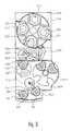
- FIG. 2is a schematic illustration of an exemplary process tool 12 .
- Process tool 12comprises a work-in-process (WIP) module 102 coupled to a robot module 104 .
- WIPwork-in-process
- a first reactor module 106 and a second reactor module 108are coupled to robot module 104 .
- Work-in-progress module 102in one embodiment includes a multilevel storage module 110 in which each level contains a number of cassettes 112 .
- Each cassette 112holds a plurality of semiconductor wafers 114 .
- there are three levels in the storage module 110each level holding eight cassettes 112 , with each cassette holding twenty-five semiconductor wafers 114 .
- Robot module 104is the wafer handling system of the embodiment of FIG. 2 .
- Robot module 104has a robot arm 116 that is operable to remove wafers 114 from cassettes 112 to load into one of the reactor modules 106 and 108 .
- Robot arm 116can also move wafers 114 from one reactor module to another.
- Robot module 104operates under control of the control computer 16 via one or more local controllers.
- First reactor module 106comprises a reactor carousel 118 having multiple positions 120 a - 120 c that accept wafers 114 .
- Each position 120 a - 120 ccan include a quartz boat 122 for holding wafers.
- reactor carouselhas three positions set apart approximately 120° from each other.
- Reactor module 106includes an elevator 124 that will raise the quartz boat 122 into a reactor chamber disposed above the carousel 118 . Once in the reactor chamber the wafers 114 in the quartz boats 122 undergo a processing step such as chemical vapor deposition and the like.
- Reactor carousel 118in one embodiment includes three positions: a wafer load and unload position 120 a , facing the robot module 116 , a process position 120 b whereby the wafers 114 in the quartz boat 122 can be moved to the reactor chamber by elevator 124 and a cool down position 120 c .
- Reactor carousel 118can rotate moving the quartz boat 122 between the positions.
- two quartz boatsare present in the reactor module, so that during processing of a first boat with wafers in the reactor chamber, a second boat with wafers, previously processed, can cool down at the cool-down position, processed wafers can be unloaded from the boat at the wafer load and unload position into the cassettes of the WIP module 102 and to be processed wafers can be loaded into the boat.
- carousel 118can rotate 120° and the prepared second boat can be elevated in the reaction chamber directly, without any loss of time.
- Second reactor module 108is similarly configured.
- An advantage of multiple positions on a carousel utilizing multiple boatsis an increased efficiency by allowing the loading and unloading of batches and the cool down of batches in parallel with the processing of other batches.
- problemscan occur in this system. If a problem occurs in processing a batch of wafers, it is important to stop the process before the next batch is loaded into a processing station so as not to spoil the wafers of the next batch.
- the control computer 16must be able to control the operation of process tool 12 when a problem occurs that requires the stoppage of loading a next load of wafers for processing. This is discussed in further detail below.
- FIG. 3is a schematic drawing of another embodiment of a process tool 12 .
- process tool 12includes a load port section 302 , a work-in-progress (WIP) section 304 , a wafer handling robot section 306 and a reactor carousel section 308 .
- WIPwork-in-progress
- Load port section 302comprises a left load port 310 and a right load port 312 .
- Cassettesalso known as front-opening unified pods 314 (FOUP), containing wafers 114 to be processed, are loaded into the left load port 310 and the right load port 312 .
- FOUPfront-opening unified pods 314
- the difference between a cassette and a FOUPis not relevant. Both are used to hold wafers prior to and after processing. Therefore, the terms “cassette” and “FOUP” will be considered as equivalent and can be used interchangeably.
- Load port section 302includes shields 316 that separate the load port section from the operator's area external to the process tool 12 .
- WIP section 304includes a FOUP-handling robot 318 that has a FOUP gripper 320 for attaching to FOUPs 314 .
- WIP section 304also includes a FOUP stocker carousel 322 that is designed to hold FOUPs 314 on one or more levels.
- An upper transfer module 326transfers FOUPs 314 to an upper load port 328 and a lower transfer module, disposed below the upper transfer module 326 and not visible in the top view drawing of FIG. 3, transfers FOUPs to a lower load port, not visible, and disposed below upper load port 328 .
- FOUP handling robot 318transfers FOUP 314 from left load port 310 and right load port 312 to the FOUP stocker carousel 322 .
- FOUP handling robot 318also can transfer FOUP 314 from the FOUP stocker carousel 322 to the position 325 on upper transfer module 326 and to a corresponding position on the lower transfer module (not pictured). Then these modules are rotated in order for the FOUPs 314 to attach to upper load port 328 or the lower load port (not pictured).
- Wafer handling robot section 306includes a wafer handling robot 330 that removes wafers from FOUPs 314 and loads them onto a quartz boat 332 that can the be moved to the reactor carousel section 308 .
- Reactor carousel section 308includes, in one embodiment, a four-position reactor carousel 334 , with each carousel position operable to hold a quartz boat 332 .
- Reactor carousel section 308includes two reactor positions 336 where the quartz boat 332 can be lifted into one of the two reactors disposed above the two reactor positions 336 by one of the elevators 324 so that the wafers of the quartz boat 332 can undergo a processing step such as the formation of an oxide layer.
- the reactor carousel section 308includes a boat input/output position 338 where a boat of wafers can be loaded onto the carousel 334 or removed from the carousel by boat transfer mechanism 333 .
- a staging station 340where wafers can cool-down after being processed in a reactor.
- the two reactorscan be used in parallel, such that wafers receive processing in one of the two reactors. It is also possible that wafers are processed sequentially in both reactors, first in one reactor and then in the other reactor. Sequential processing is known as tube-to-tube processing. In the system of FIG. 3, tube-to-tube processing is very efficient because it is not necessary to unload and reload the wafers from and into the quartz boat between the sequential processes.
- FIG. 4is a flowchart for the operation of the process tool of FIG. 2 and FIG. 3 .
- a batchis defined.
- the batchis defined as one or more lots of wafers as supplied in one or more cassettes or FOUPs. Typically, a batch of wafers is equal to or less than the number of wafers that can be placed on a single boat for processing. Further, in the define step it is determined which processing the wafers should receive.
- the batchis queued for processing by operator input, which means that processing or loading will be started automatically as soon as the previous batch has been progressed so far that the system is available to start processing or loading the next batch.
- Part of the queuing processis the downloading of certain information to certain tool controllers in the process tool that are involved in the movement and processing of the semiconductor wafers.
- the queuingis performed via the master control station (MCS) and information is downloaded to the robot logistic controller (RLC) because both controllers are involved in the logistics.
- MCSmaster control station
- RLCrobot logistic controller
- the systemcan be programmed such that loading of the wafers onto a boat can start during processing of the previous batch in the reaction chamber. This saves time because the boat can now be loaded into the reactor chamber as soon as the previous batch is removed from the reactor chamber.
- CAMcomputer aided manufacturing
- the batchis loaded into the WIP module 102 by inserting cassettes into the WIP carousel 118 , in step 408 for the embodiment of FIG. 2 .
- the FOUPs 314are first loaded into load ports 310 and 312 . These FOUPs 314 are then loaded into WIP module 304 by FOUP handling robot 318 .
- step 420wafers are transferred from cassettes to a wafer boat.
- robot arm 116moves the wafers from those cassettes in the WIP module 102 that are part of the batch to a quartz boat on the carousel.
- the FOUPs 314are moved to a FOUP load port 328 where the wafers are removed from the FOUPs 314 by the FOUP handling robot arm 330 and placed in quartz boat 332 .
- step 450the boat, loaded with wafers, is transferred to the reactor chamber.
- thisis done by rotation of the carousel 118 and movement of the elevator 124 .
- the boat loaded with wafersneeds to be transferred to the carousel 334 by boat transfer mechanism 333 and then the carousel transports the boat by rotation to the reactor concerned and the corresponding elevator 324 moves the boat into the reaction chamber.
- step 460the batch of wafers is processed in the reactor.
- Step 470also comprises the cool-down of the boat at the cool-down position and the transfer of the boat to the unload position.
- the robot armunloads the wafers from the boat and back into cassettes or FOUPs. After completion of the wafer transfer from the boat to the cassettes or FOUPs, the cassettes or FOUPs are removed from the system in step 490 . The process is completed in step 499 .
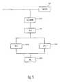
- FIG. 5is a block diagram of the communication architecture of the exemplary process tool 12 .
- a computer aided manufacturing (CAM) host 501is operable to connect with and communicate with a plurality of process tools 12 via a cell controller 502 .
- the process tool 12is controlled by a master control station (MCS) 504 .
- MCS 504is coupled to a plurality of digital process controllers including first digital process controller 506 and a second digital process controller 508 .
- Each digital process controlleris associated with a reactor such that first digital process controller 506 is associated with a first reactor and the second digital process controller 508 is associated with a second reactor.
- the digital process controllerscontrol the process parameters like gas flows, pressure, temperature and the like.
- a robot and logistic controller (RLC) 510is coupled to first digital process controller 506 and second digital process controller 508 .
- Master control station 504in one embodiment is a computer based control station running an operating system such as OS2 or Windows 2000.
- the master control station 504is operable to run a control program controlling the operation of the process tool 12 .
- Master control station 504is, in one embodiment, the control computer 16 of FIG. 1 .
- Master control station 504is operable to run a graphical user interface to allow an operator to monitor and control the function of a process tool 12 .
- the master control station 504communicates with all other controllers through the digital process controllers 506 , 508 for each reactor.
- Digital process controllers 506 , 508run and execute the process program.
- digital process controllers 506 , 508are coupled to master control station 504 via a serial connection such as a RS-422 serial communication link.
- a serial connectionsuch as a RS-422 serial communication link.
- Other communication links, serial or parallel, wired or wirelesscan also be used.
- Robot logistics controller 510in one embodiment, such as the one illustrated in FIG. 2, controls the wafer-handling robot and manages the WIP section of the cluster tool.
- additional controllers similar to, and in communication with, robot and logistic controllermay be utilized to control other robotic components such as the FOUP-handling robot.
- the exact configuration of the control systemwill vary depending on the complexity of the system and design choices. For example, all the control functions for the tool can be performed by only one computer, or alternatively, more sub-controllers can be used than shown in FIG. 5 .
- Additional controllersmay also be present in the process tools. These include temperature controllers for monitoring and regulating process temperature and motion controllers for monitoring and regulator carousel movement and reactor elevator movement.
- a production control system (PCS) programis running on master control station (MCS) 504 .
- MCSmaster control station
- MCSmaster control station
- the PCS program running on the MCS 504along with worker input, can initiate the process of batches of wafers through the define batch step 402 and the queue batch step 406 as shown in FIG. 4 .
- Commandsare sent to the digital process controller and the robot and logistic controller to control the loading of cassettes, the movement and process of wafers and the unloading of cassettes.
- the MCS 504is monitoring for the generation of an inhibit next load flag.
- An inhibit next load flagis a flag in the software caused by one or more events that will not effect already started processing in the reactor chamber but prohibit the next batch of wafers from being processed. It will also prevent loading of the wafers of a next batch into a boat, if the wafer transfer has not yet started. This saves the unprocessed wafers from potential damage.
- the MCS 504receives the inhibit next load flag, certain steps, initiated either by an operator or by the process control program can take place. The causes of the inhibit next load flag and corrective actions available after an INL flag is set are discussed in further detail below.
- FIG. 6is a flowchart that shows different ways in which an inhibit next load (INL) flag can be set.
- the INL flagis set in the real time layer.
- the real time layercomprises the digital process controllers 506 , 508 , the robot and logistic controller 510 and other controllers necessary in the process tool and involved in monitoring and controlling the process parameters and other conditions in the process tool.
- Alarmscan be defined indicating that a process parameter or other condition deviates from a desired value. Further, it can be defined if the occurrence of a certain alarm should result in the generation of an inhibit next load flag.
- the setting of an INL flag in the real time layerindicates that a situation has occurred that is not favorable for the process result.
- the process resultmight still be within the required specification limits, there is an increased risk that a situation will develop that requires an immediate process interruption, with all the disadvantages and damage to the wafers concerned, which should be prevented.
- the INL flagis set in box 610 .
- the INL flagmay be set by a higher level computer, to which the master control station of the process tool is connected, like a computer aided manufacturing (CAM) host computer system.
- the CAM host computermay control a number of tools on an assembly line, including a process tool.
- a user of the process toolhas one or more reasons that require the system to be halted. Examples include scheduled preventative maintenance routines that need to be run, problems with a downstream process tool in the manufacturing line, requiring the suspension of one or more upstream process tools, or the results of a wafer analysis on a wafer inspection tool of a wafer previously processed on the tool, the results being collected and evaluated via the CAM host and found to be outside the specification limits.
- the condition on which the inhibit next load flag should be generatedcan be pre-programmed but can also be generated by manual input into the host computer. When the condition for generation of the INL flag is fulfilled, the INL flag is generated in box 610 .
- the INL flagis set by an alarm on a composed variable.
- a composed variableis a user defined expression that can include one or more process parameters and measurement data. Examples are the average value of a real time process parameter during a certain recipe step, the time required to pump down a reactor chamber to a certain pressure, or a trend in deposited film thickness for subsequent runs.
- the composed variable alarmsare designed to look at composed variables and determine if the parameters are such that the next batch of wafers should be processed or not. Examples of composed variable alarms include measurement data on a wafer which are still within the specification limits but show a systematic trend and deviate increasingly from a target value. If a composed variable alarm condition occurs for which the setting of an inhibit next load flag is specified, the inhibit next load flag is set in box 610 .
- an operatorcan manually set an inhibit next load flag by click button pushing or other input into the master control station via its operator interface.
- the inhibit next load flagis set in box 610 .
- FIG. 7is a flow chart illustrating the use of a INL flag in the process sequence as shown in FIG. 4 . Similar steps are indicated with similar reference numbers.
- the define batch step 702 , the queue batch step 706 and the load cassettes into tool step 708were already explained in the context of FIG. 4 .
- the systemis continuously monitoring to see if an INL flag has been set. When this is the case prior the queue batch step 706 , or even prior to the define batch step 702 , the INL flag will halt the system so that continuation is not possible. Consequently, if an INL flag has been set it will not be possible to define a batch, or when the batch was already defined but not queued, it will not be possible to queue the batch.
- step 712it is checked if an INL flag has been set. If so, the system will be halted. During halting of the system it is continuously checked if the INL flag is still set as indicated by block 712 , and if the INL flag is overruled, as indicated by block 714 . When overruled, the system will resume the sequence and continue with the next step.
- step 720the loading of a wafer, or, in the case of batch processing, the loading of multiple wafers is indicated.
- INL flagis set as indicated by block 722 and a check if the INL flag has been overruled takes place as indicated by block 723 .
- processingis understood to be subjecting one or more wafer in a process chamber to a process.
- the start of the processis when the actual “subjecting one or more wafers in a process chamber to a process” starts and the logistics prior to the processing are distinguished from the process.
- the INL flagis set at some moment in time prior to the start of the processing in the reaction chamber, a choice can be made between immediate halting the progress of the next batch or delay the halting of the next batch, such that the start of actual processing is prevented. Further, halting of the progress leaves a partially transferred batch in the system which is undesired. In the example of FIG. 7, the progress is not immediately halted and options are available so that after halting a batch, the wafers that were already transferred from a cassette to the boat are returned to the cassettes.
- an unload timeris started.
- the time counted down by the unload timeris selectable. It is possible to select a zero time, a finite time such as 15 minutes, or an infinite time.
- an auto recovery procedurewill start as indicated in block 725 such that the system ends in a defined state.
- the auto recovery procedure usedis that the boat is unloaded and the wafers are returned to the cassettes.
- other auto recovery procedurescan be programmed depending on the exact system configuration.
- the unload timerWhen the unload timer is not expired, it is checked in block 726 if the operator has pushed the unload button to begin immediate unload of the loaded but unprocessed wafers. If so, unloading starts immediately, without waiting for the expiration of the timer. If not, and in the case that the INL flag has been overruled, it will be checked if the loading is complete, as indicated in block 728 . When the loading is not complete, a next wafer will be loaded to the boat and the loop starts again. When the wafer loading is complete it will be checked again if the INL flag is set in block 732 . If not, the sequence will go to the next step which is loading the boat into the reaction chamber as indicated by block 750 .
- the INL flagWhen the INL flag is set it is checked if the INL is overruled as indicated by block 733 . If so, the system also continues with loading the boat into the reaction chamber as indicated by block 750 . If the INL flag is not overruled, the system will wait until the unload timer is expired or the operator pushes the unload button for immediate unload, as indicated by blocks 734 , 735 and 736 and the corresponding connections. Alternatively, the INL flag can disappear before unloading starts. In that case the system after all resumes processing and proceeds to block 750 .
- the boat elevation stepis part of the process recipe which makes it rather obvious to select the start of the boat elevation step as the start of the process.
- the reactor chambersare furnaces, and loading the boat into the reactor exposes the wafers to a thermal budget, which is undesirable if the corresponding actual process is not carried out.
- other choicescan be made. For other systems it is possible that even after placing a wafer in the process chamber and before starting the actual processing, possible interruption of the sequence by the INL flag can be programmed.
- FIG. 8 and FIG. 9are block diagrams illustrating in an other way what happens after an INL flag has been set and which options are available for an operator.
- Block 800indicates that an INL flag has been set.
- block 810it is checked if the batch is already queued. If not, the only option available is “Reset INL”, as indicated in block 814 . However, if the alarm condition, resulting in the INL, is still active, it will not be possible to reset the INL flag because it is instantaneously set again. In alternative cases, when an INL has been generated by some step in the total sequence, different from the current step, it will be possible to reset the INL but it will be set again when the sequence passes that step again.
- the options “Reset INL”, “Overrule INL”, and “Initiate unloading”are available, as indicated by block 834 .
- the Auto recovery procedureis immediately started, without further waiting for the expiration of the unload timer.
- FIG. 9the specific situation of a tube-to tube process is addressed.
- two processesare scheduled in the tool sequentially: first the wafers undergo processing in a first reactor chamber and then the wafers undergo processing in a second reactor chamber in the same tool.
- a special situationoccurs when the first process in the first tube has been completed and an INL flag is set for tube 2 .
- the possible optionsare given by FIG. 9 .
- the starting situationis indicated, whereas in block 836 the available options are indicated.
- “Reset INL”, “Overrule INL”, and “Initiate unloading to WIP”there is the option “Initiate unloading to empty boat of tube 2 ”.
- This last optioncan be used when it is expected that processing in tube 2 can be resumed soon.
- an additional flagcan be used called the “Confirmation flag”.
- the confirmation flagis used as a positive confirmation that processing can go forward.
- this confirmation flagcan be used as a final approval before the actual processing starts. The approval is obtained from the measurement of a previously processed wafer and analysis of the results and comparison of the results with specification limits. Schematically this is illustrated in the flowchart of FIG. 10 .
- a wafer of batch Nwhere N is an integer number representing a current batch is analyzed after processing.
- the wafersare examined in a wafer inspection system that is connected to the process tool.
- a wafer inspection stationcould be integrated in communication with the wafer handling robot section such that the wafer handling robot can move wafers into the inspection system.
- the measurement systemcan include an optical system to measure the thickness of the film formed on the wafer during the process.
- the measurement systemcan include a vision system including a video camera attached to a microscope lens apparatus for examining the surface of the wafer.
- Other componentscan also be present to assist in qualitative and quantitative measurements.
- the measurementcan be performed according to an integrated metrology(IM) recipe defining what part of the wafer is being examined as well as, the parameters used and the criteria used to decide if the result is within the specification limits.
- IMintegrated metrology
- This IM recipemay be permanently present in the code being run on the master control station 504 , or, alternatively, the recipe can be downloaded from a higher level controller such as the CAM host when the IM recipe is needed.
- the wafersundergo examination.
- the wafer IDis read off the wafer by the vision system.
- a number of points on the waferare chosen and the thickness of the applied layer (such as an applied oxide layer) is measured.
- the number of pointscan be predetermined by the measurement recipe or selected by the operator of the tool.
- Informationsuch as the thickness at each point, the mean thickness, the median thickness and the maximum value, the minimum valve and the standard deviation can be calculated. Any of these values can be compared to a predetermined specification limits and to determine if the measurements are within or outside of the specification limits and if the confirmation flag can be set to “true” and if an INL flag needs to be set.
- An alternative measurementmight be the number of particles on the wafer. This required a particle counter.
- the measurement systemlocates and measures particle defects on the surface of the processed wafer. Again, the particle count can be compared with the specification limits for particle counts and it can be determined if the confirmation flag can be set to “true” or if an INL flag should be set.
- the resultsare sent to the MCS in step 875 .
- the process analysis program running on the MCSdetermines, in conjunction with the measurement recipe and the data from the measurements, if the results are with the specification limits. When the results are within the specification limits, the Confirmation flag can be set “true”, as indicated by block 878 .
- the confirmation flagis left as “false”, which is the state the confirmation flag is set when a batch is defined as seen in FIG. 11, step 1102 and an INL flag can be set as indicated by block 877 . All of these steps can be performed in the method as shown in the following figure, FIG. 10, at step 872 .
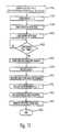
- FIG. 11a complete sequence is given with the use of a Confirmation flag.
- the sequenceis based on the sequence of FIG. 4, wherein identical steps are indicated by identical reference numerals.
- the steps that are common to FIG. 4are discussed in detail in conjunction with FIG. 4 .
- Some stepsare added and some steps are slightly changed.
- the first two stepsare now called “Define batch N+1”, step 1102 , and “Queue batch N+1”, step 1106 where N is an integer number.
- a checkis performed before the start of the actual processing a check is performed if the Confirmation flag is set, as indicated by step 838 . In our case the check is performed before loading the boat into the reaction chamber but it can also be performed at an earlier stage or a later stage as long as it is performed prior to the start of the actual process.
- Step 872comprises the steps as shown in FIG. 10, but now for batch N+1.
- the Confirmation flag functionat the beginning of the sequence it should be set to “false”. This is done in the “Define batch N+1” step 1102 .
- the Confirmation flagis already set to “true”, it is in fact switched off and has no function anymore.
- the present inventionincludes a method for the processing of one or more wafers in a process tool.
- one or more wafers in a reaction chamberare subjected to a process.
- a software implemented “confirmation flag”is provided.
- the confirmation flagis set in a “false” state for the one or more to be processed wafers.
- a wafer inspection toola wafer previously processed in said reaction chamber is examined and the results are compared against an acceptance criteria. If the results are within the acceptance criteria, the confirmation flag is set to a “true” state. When the results are outside the acceptance criteria the confirmation flag is left in or set to a “false” state.
- the confirmation flagPrior to the start of the processing of one or more to be processed wafers, the confirmation flag is checked to see if it is in a “true” state. If the confirmation flag is in a “false” state, the start of the processing of the one or more to be processed wafers is prohibited.
- the present inventionincludes a process tool for the processing of one or more wafers.
- the process toolincludes at least one reactor chamber for processing one or more wafers and a system controller having a processor and memory and operable to execute a process control system program and to monitor and control processing tool parameters.
- a wafer inspection stationis coupled to the processing tool and coupled to the system controller.
- the wafer inspection stationis operable to examine a wafer previously processed in the reaction chamber.
- the wafer inspection stationgenerates wafer data and send the wafer data to the system controller.
- the system controlleris operable to compare the wafer data against predefined limits and set a confirmation flag in a “true” state when the wafer data are within the predefined limits. Otherwise, the confirmation flag is set or left in a “false” state when the wafer data are outside the predefined limits.
- the start of the processing of the one or more to be processed wafersis prohibited when the confirmation flag is in a false state.
- FIG. 12is a flowchart illustrating a sequence wherein both an INL flag and a confirmation flag are used.
- the flowchartresembles to a large extent the flowchart of FIG. 7 and identical steps are indicated with identical reference numerals.
- step 838a check if the confirmation flag has been set is made. If the confirmation flag is not set, the system will wait in a loop, continuously checking the INL flag is set and the confirmation flag is set. If both the conditions “INL flag not set” and “Confirmation flag set” are fulfilled, the system proceeds to the next step 750 , “Loading boat into reactor chamber” as seen in FIG. 7 .
- wafer inspection instrumentsWhen wafer inspection instruments are used to analyze the wafer, these wafer inspection instruments are preferably integrated into the processing tool. However, the use of the flags according to the invention is also possible when the wafer inspection instruments are not located inside the process tools but separated from the process tool.
- the resultscan be analyzed by a computer connected to the wafer inspection instrument and the outcome can be coupled to the master control station 504 via the CAM host or similar system.
Landscapes
- Engineering & Computer Science (AREA)
- Automation & Control Theory (AREA)
- Physics & Mathematics (AREA)
- Condensed Matter Physics & Semiconductors (AREA)
- General Physics & Mathematics (AREA)
- Manufacturing & Machinery (AREA)
- Computer Hardware Design (AREA)
- Microelectronics & Electronic Packaging (AREA)
- Power Engineering (AREA)
- Container, Conveyance, Adherence, Positioning, Of Wafer (AREA)
Abstract
Description
This invention relates to the field of semiconductor manufacturing and more specifically to a method and system to process semiconductor wafers, to interrupt this processing if an alarm condition exists and to recover the situation after an interruption has taken place.
In automated fabrication plants or inside a complex wafer-processing tool, work pieces travel from one process station to another. At these process stations various operations are performed on the work pieces. During processing certain events may occur that will require the system to shutdown or at the very least temporarily pause processing. These may include problems in a process station detected by examining the output of the process station or by detection of out of specification parameters in a system, among other problems. When this occurs, it is necessary to halt the processing of wafers in the system to prevent further damage. However, when the processing is halted, wafers of which the processing is halted may still be present in the system. These wafers block the continuation of further processing in the system after the alarm condition has been resolved. After resolving of the alarm condition that resulted in interruption of the process, the further processing or handling of these wafers of which the processing was interrupted needs to be defined before the system can be used for continued processing. Therefore, there is a need for a way to monitor for and handle conditions that require the interruption of processing in a process tool and, after interruption, the recovery of the system and continuation of further processing.
Part of this problem is addressed in U.S. Pat. No. 6,162,010 issued to Ishizawa et al. and entitled “Method of Recovering Object to be Treated After Interruption”. This patent discusses the recovery of a semiconductor wafer after a treatment is unexpectedly stopped for a reason such a loss of power to the processing machinery. This patent discloses recovering wafers to an original cassette if the wafers are cooled and allowing the wafers to cool if the wafers were in a reactor-processing chamber. This method suffers from several drawbacks. First, it is drawn to a single wafer processing system and is not easily adaptable to batch processing. Second the recovery method is rigid and does not allow for override by operator or temporary suspension.
International Publication WO 01/18623 A1 entitled “Real-Time Fault Detection” discloses a method for detecting faults in semiconductor wafers in a real time environment. In this disclosure, a method and system for determining if there are faults within a system is disclosed. If a fault in the manufacturing system exists, that information is sent to an interface that could shut down the process or provide information to an operator. Drawbacks to this invention include its lack of ability to override a fault detection or to handle a fault detection in a variety of ways.
Another approach is disclosed in U.S. Pat. No. 5,897,710 issued to Sato et al. entitled “Substrate Processing Apparatus and Substrate Processing Method”. In the invention of Sato et al, an inspection station is included with a processing system. The inspection station is able to inspect the wafers. When wafers fail inspection, further processing can be interrupted immediately.
A disadvantage of the methods described above is that the action of immediate interruption of a process might in itself create damage because the work pieces concerned receive only a partial treatment. It is questionable if completion of the treatment in a later stage will result in the desired end effect, without complications and negative side effects.
It is the objective of the present invention to provide in a system an method to deal with an alarm condition in a way that prevents the necessity of immediate process interruption and its disadvantages and to provide in pre-programmed, operator selectable recovery procedures after interruption has taken place.
The object of the invention is achieved by providing an alarm level that allows continuing already started processing but prevents the start of processing of next batches.
In one embodiment, a method and system for processing one ore more wafers in a process tool is provided including subjecting the one or more wafer in a reaction chamber to a process. The method includes generating an inhibit next load flag (INL flag) on predefined conditions, the inhibit next load flag not effecting already started processing of a wafer. Prior to the start of the processing of a wafer, a check is performed to see if an inhibit next load flag has been set. When upon checking it has been found that an inhibit next load has been set, the start of the process is prohibited. The method further includes providing pre-programmed recovery procedures, such that after execution of a pre-programmed recovery procedure the to be processed wafer of which the start of the processing is prohibited ends in a defined state such that the tool can be used for further processing. In another embodiment, a method and system for the batch-wise processing of wafers in a process tool is provided including subjecting the wafers batch-wise to a process in a reaction chamber. The method includes generating an inhibit next load flag on predefined conditions, the inhibit next load flag not effecting already started processing of a wafer batch. Prior to the start of the processing of a wafer batch, a check is performed to see if an inhibit next load flag has been set. When upon checking it has been found that an inhibit next load has been set, the start of the process of the wafer batch in the reaction chamber is prohibited. The method further includes providing pre-programmed recovery procedures, such that after execution of a pre-programmed recovery procedure the to be processed wafer batch of which the start of the processing is prohibited ends in a defined state such that the tool can be used for further processing.
In yet another embodiment, a method and system for processing one ore more wafers in a process tool is provided including subjecting the one or more wafer in a reaction chamber to a process. The method includes setting as a default a confirmation flag in a “false” state, and examining in a wafer inspection tool a wafer previously processed in said reaction chamber and comparing the results against acceptance criteria and setting the confirmation flag in a “true” state when said results are within the acceptance criteria. The start of the processing in the reaction chamber is only allowed when the confirmation flag is in a “true” state.
Technical benefits of the present invention include that immediate interruption of an already started process is prevented as much as possible. Although immediate interruption still remains available as an option and might be used when sudden severe problems occur, like power failure, in many cases alarm conditions indicate a potential problem that needs attention. Without paying attention, such a condition might develop into a more severe problem. According to the invention the processing is interrupted prior to the start of the processing and therefore, damage to the wafers is prevented and another attempt to continue processing can be made at a later time when the alarm condition has been resolved. Further, the pre-programmed recovery procedures, including operator selectable recovery procedures, allow a very smooth and flexible recovery of the system to prepare it for further processing. Other technical benefits are apparent from the following descriptions, illustrations and claims.
Non-limiting and non-exhaustive preferred embodiments of the present invention are described with references to the following figures wherein like reference numerals refer to like parts throughout the various views unless otherwise specified.
FIG. 1 is a block diagram of amanufacturing system 10 in accordance with the teachings of the present invention
FIG. 2 is a schematic illustration of an exemplary process tool;
FIG. 3 is a schematic drawing of another embodiment of a process tool;
FIG. 4 is a flow chart for the operation of the process tool of FIG.2 and FIG. 3;
FIG. 5 is a block diagram of the communication architecture of an exemplary process tool;
FIG. 6 is a flow chart that shows different ways in which an inhibit next load (INL) flag can be set;
FIG. 7 is a flow chart illustrating interruption of a batch process sequence by an inhibit next load flag;
FIG. 8 is a block diagram illustrating the operator selectable options after the interruption of a process by an inhibit next load (INL) flag;
FIG. 9 is a block diagram illustrating the operator selectable options after the interruption of a process by an inhibit next load (INL) flag in a specific tube-to-tube case;
FIG. 10 is a flow chart illustrating the execution of an integrated metrologyrecipe;
FIG. 11 is a flow chart illustrating the use of a confirmation flag prior to the start of a process;
FIG. 12 is a flow chart illustrating the simultaneous use of an inhibit next load (INL) flag and a confirmation flag in a batch process sequence.
A method of the present invention includes a method to prohibit the loading and processing of wafers prior to the start of processing when an error in the process tool occurs. The method can be used in any one of a number of systems where work pieces are processed in a processing station. The method can be used for single wafer processing tools and for batch processing tools. Further, the method can advantageously be applied on tools comprising a plurality of processing stations. Interruption of the processing in such a multi-station tool requires an elaborate recovery procedure to bring the wafers of which the processing has been interrupted in a defined state and the present invention can be beneficially applied to such multi-station process tools. The examples presented in the following figures relate to batch furnaces and are for illustrative purposes only and are not intended to limit the application of the present invention to such examples.
For example, FIG. 1 is a block diagram of amanufacturing system 10 in accordance with the teachings of the present invention.Manufacturing system 10 includes aprocess tool 12 coupled to acontrol computer 16 via input/output line 14 and adisplay 20 coupled to thecontrol computer 16 via input/output line 18.
FIG. 2 is a schematic illustration of anexemplary process tool 12.Process tool 12 comprises a work-in-process (WIP)module 102 coupled to arobot module 104. Afirst reactor module 106 and asecond reactor module 108 are coupled torobot module 104.
Work-in-progress module 102 in one embodiment includes amultilevel storage module 110 in which each level contains a number ofcassettes 112. Eachcassette 112 holds a plurality ofsemiconductor wafers 114. In one embodiment, there are three levels in thestorage module 110, each level holding eightcassettes 112, with each cassette holding twenty-fivesemiconductor wafers 114.
An advantage of multiple positions on a carousel utilizing multiple boats is an increased efficiency by allowing the loading and unloading of batches and the cool down of batches in parallel with the processing of other batches. However, problems can occur in this system. If a problem occurs in processing a batch of wafers, it is important to stop the process before the next batch is loaded into a processing station so as not to spoil the wafers of the next batch. Thus, thecontrol computer 16 must be able to control the operation ofprocess tool 12 when a problem occurs that requires the stoppage of loading a next load of wafers for processing. This is discussed in further detail below.
FIG. 3 is a schematic drawing of another embodiment of aprocess tool 12. In this embodiment,process tool 12 includes aload port section 302, a work-in-progress (WIP)section 304, a waferhandling robot section 306 and areactor carousel section 308.
Wafer handlingrobot section 306 includes awafer handling robot 330 that removes wafers fromFOUPs 314 and loads them onto aquartz boat 332 that can the be moved to thereactor carousel section 308.
FIG. 4 is a flowchart for the operation of the process tool of FIG.2 and FIG.3. In afirst step 402, a batch is defined. The batch is defined as one or more lots of wafers as supplied in one or more cassettes or FOUPs. Typically, a batch of wafers is equal to or less than the number of wafers that can be placed on a single boat for processing. Further, in the define step it is determined which processing the wafers should receive. Instep 406, the batch is queued for processing by operator input, which means that processing or loading will be started automatically as soon as the previous batch has been progressed so far that the system is available to start processing or loading the next batch. Part of the queuing process is the downloading of certain information to certain tool controllers in the process tool that are involved in the movement and processing of the semiconductor wafers. In the exemplary tools of FIGS. 2 and 3, the queuing is performed via the master control station (MCS) and information is downloaded to the robot logistic controller (RLC) because both controllers are involved in the logistics. Beneficially, the system can be programmed such that loading of the wafers onto a boat can start during processing of the previous batch in the reaction chamber. This saves time because the boat can now be loaded into the reactor chamber as soon as the previous batch is removed from the reactor chamber. Also, in the batch definition and queuing steps a computer aided manufacturing (CAM) host can be involved to ensure that a batch receives the required processing and that operator errors in batch definition are omitted. The connections between the (CAM) host, master control station and robot logistic controller is illustrated in FIG.5.
The batch is loaded into theWIP module 102 by inserting cassettes into theWIP carousel 118, instep 408 for the embodiment of FIG.2. For the embodiment of FIG. 3, theFOUPs 314 are first loaded intoload ports FOUPs 314 are then loaded intoWIP module 304 byFOUP handling robot 318.
Instep 420 wafers are transferred from cassettes to a wafer boat. For the embodiment in FIG. 2,robot arm 116 moves the wafers from those cassettes in theWIP module 102 that are part of the batch to a quartz boat on the carousel. For the embodiment of FIG. 3, theFOUPs 314 are moved to aFOUP load port 328 where the wafers are removed from theFOUPs 314 by the FOUPhandling robot arm 330 and placed inquartz boat 332.
Instep 450, the boat, loaded with wafers, is transferred to the reactor chamber. For the embodiment of FIG. 2, this is done by rotation of thecarousel 118 and movement of theelevator 124. For the embodiment of FIG. 3, first the boat loaded with wafers needs to be transferred to thecarousel 334 byboat transfer mechanism 333 and then the carousel transports the boat by rotation to the reactor concerned and thecorresponding elevator 324 moves the boat into the reaction chamber. Then, instep 460, the batch of wafers is processed in the reactor.
After processing, the boat is unloaded from the reactor chamber and the reactor carousel rotates to move the batch to the cool down position, instep 470. Step470 also comprises the cool-down of the boat at the cool-down position and the transfer of the boat to the unload position. Instep 480, the robot arm unloads the wafers from the boat and back into cassettes or FOUPs. After completion of the wafer transfer from the boat to the cassettes or FOUPs, the cassettes or FOUPs are removed from the system instep 490. The process is completed instep 499.
FIG. 5 is a block diagram of the communication architecture of theexemplary process tool 12. A computer aided manufacturing (CAM)host 501 is operable to connect with and communicate with a plurality ofprocess tools 12 via acell controller 502. Theprocess tool 12 is controlled by a master control station (MCS)504.MCS 504 is coupled to a plurality of digital process controllers including firstdigital process controller 506 and a seconddigital process controller 508. Each digital process controller is associated with a reactor such that firstdigital process controller 506 is associated with a first reactor and the seconddigital process controller 508 is associated with a second reactor. The digital process controllers control the process parameters like gas flows, pressure, temperature and the like. A robot and logistic controller (RLC)510 is coupled to firstdigital process controller 506 and seconddigital process controller 508.
In operation, a production control system (PCS) program is running on master control station (MCS)504.Master control station 504 displays a graphical user interface to facilitate work interaction. The PCS program running on theMCS 504 along with worker input, can initiate the process of batches of wafers through the definebatch step 402 and thequeue batch step 406 as shown in FIG.4. Commands are sent to the digital process controller and the robot and logistic controller to control the loading of cassettes, the movement and process of wafers and the unloading of cassettes. At the same time, theMCS 504 is monitoring for the generation of an inhibit next load flag. An inhibit next load flag (INL flag) is a flag in the software caused by one or more events that will not effect already started processing in the reactor chamber but prohibit the next batch of wafers from being processed. It will also prevent loading of the wafers of a next batch into a boat, if the wafer transfer has not yet started. This saves the unprocessed wafers from potential damage. When theMCS 504 receives the inhibit next load flag, certain steps, initiated either by an operator or by the process control program can take place. The causes of the inhibit next load flag and corrective actions available after an INL flag is set are discussed in further detail below.
FIG. 6 is a flowchart that shows different ways in which an inhibit next load (INL) flag can be set. Inbox 602, the INL flag is set in the real time layer. The real time layer comprises thedigital process controllers logistic controller 510 and other controllers necessary in the process tool and involved in monitoring and controlling the process parameters and other conditions in the process tool. Alarms can be defined indicating that a process parameter or other condition deviates from a desired value. Further, it can be defined if the occurrence of a certain alarm should result in the generation of an inhibit next load flag. The setting of an INL flag in the real time layer indicates that a situation has occurred that is not favorable for the process result. Although the process result might still be within the required specification limits, there is an increased risk that a situation will develop that requires an immediate process interruption, with all the disadvantages and damage to the wafers concerned, which should be prevented. When in the real time layer a condition occurs that is programmed to result in the setting of an INL flag, the INL flag is set inbox 610.
Inbox 604, the INL flag may be set by a higher level computer, to which the master control station of the process tool is connected, like a computer aided manufacturing (CAM) host computer system. The CAM host computer may control a number of tools on an assembly line, including a process tool. In this case, a user of the process tool has one or more reasons that require the system to be halted. Examples include scheduled preventative maintenance routines that need to be run, problems with a downstream process tool in the manufacturing line, requiring the suspension of one or more upstream process tools, or the results of a wafer analysis on a wafer inspection tool of a wafer previously processed on the tool, the results being collected and evaluated via the CAM host and found to be outside the specification limits. The condition on which the inhibit next load flag should be generated can be pre-programmed but can also be generated by manual input into the host computer. When the condition for generation of the INL flag is fulfilled, the INL flag is generated inbox 610.
Inbox 606, the INL flag is set by an alarm on a composed variable. A composed variable is a user defined expression that can include one or more process parameters and measurement data. Examples are the average value of a real time process parameter during a certain recipe step, the time required to pump down a reactor chamber to a certain pressure, or a trend in deposited film thickness for subsequent runs. The composed variable alarms are designed to look at composed variables and determine if the parameters are such that the next batch of wafers should be processed or not. Examples of composed variable alarms include measurement data on a wafer which are still within the specification limits but show a systematic trend and deviate increasingly from a target value. If a composed variable alarm condition occurs for which the setting of an inhibit next load flag is specified, the inhibit next load flag is set inbox 610.
Finally, inbox 608, an operator can manually set an inhibit next load flag by click button pushing or other input into the master control station via its operator interface. In that case, the inhibit next load flag is set inbox 610.
FIG. 7 is a flow chart illustrating the use of a INL flag in the process sequence as shown in FIG.4. Similar steps are indicated with similar reference numbers. The definebatch step 702, thequeue batch step 706 and the load cassettes intotool step 708 were already explained in the context of FIG.4. The system is continuously monitoring to see if an INL flag has been set. When this is the case prior thequeue batch step 706, or even prior to the definebatch step 702, the INL flag will halt the system so that continuation is not possible. Consequently, if an INL flag has been set it will not be possible to define a batch, or when the batch was already defined but not queued, it will not be possible to queue the batch. Further continuation is only possible when the INL flag has been removed. When the cassettes have been placed into the tool as indicated instep 708, but the wafer transfer has not been started yet, inblock 712 it is checked if an INL flag has been set. If so, the system will be halted. During halting of the system it is continuously checked if the INL flag is still set as indicated byblock 712, and if the INL flag is overruled, as indicated byblock 714. When overruled, the system will resume the sequence and continue with the next step. Instep 720 the loading of a wafer, or, in the case of batch processing, the loading of multiple wafers is indicated. After completion of the transfer of a wafer, again it is checked if an INL flag is set as indicated byblock 722 and a check if the INL flag has been overruled takes place as indicated byblock 723. However, after the wafer transfer has been started, a more difficult situation is present. The essence of the INL flag is that in case of an alarm condition a batch is halted prior to starting the actual processing. In the context of the present invention, “processing” is understood to be subjecting one or more wafer in a process chamber to a process.
The start of the process is when the actual “subjecting one or more wafers in a process chamber to a process” starts and the logistics prior to the processing are distinguished from the process. When the INL flag is set at some moment in time prior to the start of the processing in the reaction chamber, a choice can be made between immediate halting the progress of the next batch or delay the halting of the next batch, such that the start of actual processing is prevented. Further, halting of the progress leaves a partially transferred batch in the system which is undesired. In the example of FIG. 7, the progress is not immediately halted and options are available so that after halting a batch, the wafers that were already transferred from a cassette to the boat are returned to the cassettes. When an INL flag is set after loading has started, but before starting the actual processing in the reaction chamber, an unload timer is started. The time counted down by the unload timer is selectable. It is possible to select a zero time, a finite time such as 15 minutes, or an infinite time. When the INL has not been overruled, inblock 724 it is checked if the unload timer has been expired. If so, an auto recovery procedure will start as indicated inblock 725 such that the system ends in a defined state. The auto recovery procedure used is that the boat is unloaded and the wafers are returned to the cassettes. However, other auto recovery procedures can be programmed depending on the exact system configuration. When the unload timer is not expired, it is checked inblock 726 if the operator has pushed the unload button to begin immediate unload of the loaded but unprocessed wafers. If so, unloading starts immediately, without waiting for the expiration of the timer. If not, and in the case that the INL flag has been overruled, it will be checked if the loading is complete, as indicated inblock 728. When the loading is not complete, a next wafer will be loaded to the boat and the loop starts again. When the wafer loading is complete it will be checked again if the INL flag is set inblock 732. If not, the sequence will go to the next step which is loading the boat into the reaction chamber as indicated byblock 750. When the INL flag is set it is checked if the INL is overruled as indicated byblock 733. If so, the system also continues with loading the boat into the reaction chamber as indicated byblock 750. If the INL flag is not overruled, the system will wait until the unload timer is expired or the operator pushes the unload button for immediate unload, as indicated byblocks
In the example of FIG. 7, when the loading of the boat into the reaction chamber has started, the setting of an INL flag will not influence the process anymore. The boat elevation step is part of the process recipe which makes it rather obvious to select the start of the boat elevation step as the start of the process. Further, in the exemplary case, the reactor chambers are furnaces, and loading the boat into the reactor exposes the wafers to a thermal budget, which is undesirable if the corresponding actual process is not carried out. However, other choices can be made. For other systems it is possible that even after placing a wafer in the process chamber and before starting the actual processing, possible interruption of the sequence by the INL flag can be programmed.
Although in FIG. 7 the situation batch processing is illustrated, wherein a plurality of wafers is processed simultaneously, it is clear that in single wafer processing wherein a batch of wafers is processed sequentially a somewhat adapted loop is required. However, the principle remains the same: when an INL flag is set, the start of the processing of a wafer is prohibited whereas already started processing is not effected.
FIG.8 and FIG. 9 are block diagrams illustrating in an other way what happens after an INL flag has been set and which options are available for an operator. In these figures, identical functions are indicated by identical reference numerals.Block 800 indicates that an INL flag has been set. Inblock 810 it is checked if the batch is already queued. If not, the only option available is “Reset INL”, as indicated inblock 814. However, if the alarm condition, resulting in the INL, is still active, it will not be possible to reset the INL flag because it is instantaneously set again. In alternative cases, when an INL has been generated by some step in the total sequence, different from the current step, it will be possible to reset the INL but it will be set again when the sequence passes that step again. When the batch has been queued but wafer loading not started yet, as checked inblock 820, another option becomes available: “Overrule INL”, as indicated inblock 824. With the overrule function, the interruption is overruled, but only for the subject batch. For the following batches the INL flag remains fully functional. When wafer loading has started, it will be checked if loading of the boat into the reactor has started as indicated byblock 830. If so, the INL has no effect anymore and the operator does not need any options. If the loading of the boat into the reactor has not started yet, the unload timer is started, as indicated inblock 832. Before expiration of the unload timer the options “Reset INL”, “Overrule INL”, and “Initiate unloading” are available, as indicated byblock 834. Upon pushing the “Initiate unloading” button, the Auto recovery procedure is immediately started, without further waiting for the expiration of the unload timer.
In FIG. 9, the specific situation of a tube-to tube process is addressed. As discussed previously, in a tube to tube process two processes are scheduled in the tool sequentially: first the wafers undergo processing in a first reactor chamber and then the wafers undergo processing in a second reactor chamber in the same tool. A special situation occurs when the first process in the first tube has been completed and an INL flag is set fortube 2. The possible options are given by FIG.9. Inblock 802 the starting situation is indicated, whereas inblock 836 the available options are indicated. In addition to “Reset INL”, “Overrule INL”, and “Initiate unloading to WIP” there is the option “Initiate unloading to empty boat oftube 2”. This last option can be used when it is expected that processing intube 2 can be resumed soon. In the exemplary system of FIG. 2, it is important to remove a processed tool-to tool batch from the first reactor module when an INL flag is set fortube 2 because it allows at least the utilization oftube 1 in a standard single tube mode.
In addition to an INL flag, an additional flag can be used called the “Confirmation flag”. Whereas the INL flag is used to indicate a problem and prohibit the start of a process when there is a problem, the confirmation flag is used as a positive confirmation that processing can go forward. In particular, this confirmation flag can be used as a final approval before the actual processing starts. The approval is obtained from the measurement of a previously processed wafer and analysis of the results and comparison of the results with specification limits. Schematically this is illustrated in the flowchart of FIG.10. Inblock 874, a wafer of batch N where N is an integer number representing a current batch is analyzed after processing. Preferably, the wafers are examined in a wafer inspection system that is connected to the process tool. For example, in the embodiment of FIG. 3 a wafer inspection station could be integrated in communication with the wafer handling robot section such that the wafer handling robot can move wafers into the inspection system. The measurement system can include an optical system to measure the thickness of the film formed on the wafer during the process. Alternatively the measurement system can include a vision system including a video camera attached to a microscope lens apparatus for examining the surface of the wafer. Other components can also be present to assist in qualitative and quantitative measurements. The measurement can be performed according to an integrated metrology(IM) recipe defining what part of the wafer is being examined as well as, the parameters used and the criteria used to decide if the result is within the specification limits. This IM recipe may be permanently present in the code being run on themaster control station 504, or, alternatively, the recipe can be downloaded from a higher level controller such as the CAM host when the IM recipe is needed. Upon availability of the IM recipe, the wafers undergo examination. In an embodiment the wafer ID is read off the wafer by the vision system. In a typical embodiment, a number of points on the wafer are chosen and the thickness of the applied layer (such as an applied oxide layer) is measured. The number of points can be predetermined by the measurement recipe or selected by the operator of the tool. Information such as the thickness at each point, the mean thickness, the median thickness and the maximum value, the minimum valve and the standard deviation can be calculated. Any of these values can be compared to a predetermined specification limits and to determine if the measurements are within or outside of the specification limits and if the confirmation flag can be set to “true” and if an INL flag needs to be set.
An alternative measurement might be the number of particles on the wafer. This required a particle counter. In a particle counter the measurement system locates and measures particle defects on the surface of the processed wafer. Again, the particle count can be compared with the specification limits for particle counts and it can be determined if the confirmation flag can be set to “true” or if an INL flag should be set. After one or more measurements are made, the results are sent to the MCS instep 875. Then, instep 876 the process analysis program running on the MCS determines, in conjunction with the measurement recipe and the data from the measurements, if the results are with the specification limits. When the results are within the specification limits, the Confirmation flag can be set “true”, as indicated byblock 878. When the results are outside the specification limits, the confirmation flag is left as “false”, which is the state the confirmation flag is set when a batch is defined as seen in FIG. 11,step 1102 and an INL flag can be set as indicated byblock 877. All of these steps can be performed in the method as shown in the following figure, FIG. 10, atstep 872.
In FIG. 11 a complete sequence is given with the use of a Confirmation flag. The sequence is based on the sequence of FIG. 4, wherein identical steps are indicated by identical reference numerals. The steps that are common to FIG. 4 are discussed in detail in conjunction with FIG.4. Some steps are added and some steps are slightly changed. The first two steps are now called “Define batch N+1”,step 1102, and “Queue batch N+1”,step 1106 where N is an integer number. Before the start of the actual processing a check is performed if the Confirmation flag is set, as indicated bystep 838. In our case the check is performed before loading the boat into the reaction chamber but it can also be performed at an earlier stage or a later stage as long as it is performed prior to the start of the actual process. After completion of the process and unloading of the boat from the reaction chamber, an Integrated Metrology recipe is carried out for batch N+1 as indicated instep 872 to measure the result and to set the confirmation flag for the next batch. Step872 comprises the steps as shown in FIG. 10, but now for batch N+1. In order to make use of the Confirmation flag function, at the beginning of the sequence it should be set to “false”. This is done in the “Define batch N+1”step 1102. Then, at a later stage, but prior to the start of the actual processing, there might be a need to set it to “true”, based on measurement of the previous batch N and analysis of the results and comparison with predefined specification limits. When in the “Define batch N+1”step 1102 the Confirmation flag is already set to “true”, it is in fact switched off and has no function anymore.
The present invention includes a method for the processing of one or more wafers in a process tool. In the method one or more wafers in a reaction chamber are subjected to a process. A software implemented “confirmation flag” is provided. As a default, the confirmation flag is set in a “false” state for the one or more to be processed wafers. In a wafer inspection tool a wafer previously processed in said reaction chamber is examined and the results are compared against an acceptance criteria. If the results are within the acceptance criteria, the confirmation flag is set to a “true” state. When the results are outside the acceptance criteria the confirmation flag is left in or set to a “false” state. Prior to the start of the processing of one or more to be processed wafers, the confirmation flag is checked to see if it is in a “true” state. If the confirmation flag is in a “false” state, the start of the processing of the one or more to be processed wafers is prohibited.
The present invention includes a process tool for the processing of one or more wafers. The process tool includes at least one reactor chamber for processing one or more wafers and a system controller having a processor and memory and operable to execute a process control system program and to monitor and control processing tool parameters. A wafer inspection station is coupled to the processing tool and coupled to the system controller. The wafer inspection station is operable to examine a wafer previously processed in the reaction chamber. The wafer inspection station generates wafer data and send the wafer data to the system controller. The system controller is operable to compare the wafer data against predefined limits and set a confirmation flag in a “true” state when the wafer data are within the predefined limits. Otherwise, the confirmation flag is set or left in a “false” state when the wafer data are outside the predefined limits. The start of the processing of the one or more to be processed wafers is prohibited when the confirmation flag is in a false state.
FIG. 12 is a flowchart illustrating a sequence wherein both an INL flag and a confirmation flag are used. The flowchart resembles to a large extent the flowchart of FIG.7 and identical steps are indicated with identical reference numerals. Different is that in the flowchart of FIG. 12, after it is checked if the INL flag is set instep 732, instep 838, a check if the confirmation flag has been set is made. If the confirmation flag is not set, the system will wait in a loop, continuously checking the INL flag is set and the confirmation flag is set. If both the conditions “INL flag not set” and “Confirmation flag set” are fulfilled, the system proceeds to thenext step 750, “Loading boat into reactor chamber” as seen in FIG.7.
Although the use of flags to interrupt processing prior to the start of the actual processing is explained with reference to a batch processing system, it can also be applied to single wafer systems. In a single wafer processing system, typically wafers are also processed group wise, but sequentially, one after another. In that case, an INL flag should preferentially not prohibit the start of a next batch but of a next wafer. This results in the situation that part of the group of wafers to be processed will remain unprocessed but it gives the greatest security. In case of using Integrated Metrology in combination with the Confirmation flag, the analysis result of wafer N can set the Confirmation flag for wafer N+1. However, this could result in a waiting time after every wafer, which is undesirable. As a compromise between security and throughput, the system can also be programmed such that the analysis result for wafer N sets the Confirmation flag for wafer N+2. This still gives a short feed-back loop with a relatively high degree of security while it remains efficient.
When wafer inspection instruments are used to analyze the wafer, these wafer inspection instruments are preferably integrated into the processing tool. However, the use of the flags according to the invention is also possible when the wafer inspection instruments are not located inside the process tools but separated from the process tool. The results can be analyzed by a computer connected to the wafer inspection instrument and the outcome can be coupled to themaster control station 504 via the CAM host or similar system.
Having now described preferred embodiments of the invention, modifications and variations to the present invention may be made by those skilled in the art. The invention is thus not limited to the preferred embodiments, but is instead set forth in the following clauses and legal equivalents thereof.
Claims (79)
1. A method for the processing of wafers in a process tool comprising:
subjecting one or more wafers in a reaction chamber in the process tool to a process;
performing one or more of the following steps in a control computer coupled to the process tool:
a) setting an inhibit next load flag if predefined conditions occur in the process tool or by human intervention or upon input from a host computer, the inhibit next load flag not effecting the one or more wafers for which processing has started;
b) checking, prior to the start of the processing of a to be processed wafer, to see if an inhibit-next load flag has been set;
c) prohibiting to start processing, in the reaction chamber, of the to be processed wafer, if an inhibit next load flag has been set; and
d) providing pre-programmed recovery procedures, such that after execution of a pre-programmed recovery procedure the to be processed wafer of which the start of the processing is prohibited ends in a defined state such that the tool can be used for further processing.
2. The method ofclaim 1 wherein the step of providing pre-programmed recovery procedures includes the step of providing operator selectable recovery procedures.
3. The method ofclaim 2 wherein the step of providing operator selectable recovery procedures includes the step of allowing an operator to reset the inhibit next load flag if said predetermined condition is no longer true.
4. The method ofclaim 2 wherein the step of providing operator selectable recovery procedures includes the step of allowing an operator to overrule the inhibit next load flag for the immediate next to be processed wafer.
5. The method ofclaim 1 wherein the predefined condition is based on an alarm level of a real time parameter, the real time parameter representing real time conditions in the process tool.
6. The method ofclaim 1 wherein the predefined condition is based on an expression comprising one or more parameters out of a collection of a plurality of real time parameters, representing real time conditions in the process tool, and analysis results of a wafer processed prior to the to be processed wafer.
7. The method ofclaim 1 wherein the predefined condition is a “set inhibit next load flag” command, initiated by an operator command.
8. The method ofclaim 1 wherein the predefined condition is a “set inhibit next load flag” command, initiated by a higher level controller, connected to the tool controller.
9. The method ofclaim 1 wherein the to be processed wafers are supplied to the processing tool in cassettes and the step of providing pre-programmed recovery procedures further comprising initiating an automatic transfer of the to be processed wafers that has been removed from the cassette and of which the start of the processing is prohibited.
10. The method ofclaim 9 wherein the step of initiating an automatic transfer of the to be processed wafers that have been removed from the cassette and of which the start of the processing is prohibited comprises transferring said wafers to the cassette.
11. The method ofclaim 1 wherein the step of providing pre-programmed recovery procedures further comprises initiating a hold unload timer during which no automated response to the inhibit next load flag is started.
12. The method ofclaim 11 wherein the step of initiating a hold unload timer further comprises allowing operator intervention when the hold unload timer is operational.
13. A process tool for processing one or more wafers supplied, comprising:
at least one reaction chamber for subjecting the one or more wafers to a process;
a tool controller having a processor and memory and operable to execute a process control system program, the process control system program operable to monitor and control tool parameters; and
wherein the tool controller is operable to generate an inhibit next load flag upon predefined inputs and, when the inhibit next load object is generated prior to the start of the processing of a to be processed wafer, prohibit the start of the processing of the to be processed wafer in the reaction chamber, and to provide pre-programmed recovery procedures such that after execution of a preprogrammed recovery procedure the to be processed wafer ends in a defined state such that the tool can be used for further processing.
14. The process tool ofclaim 13 , wherein the tool controller comprises one or more subcontrollers, connected to the tool controller, the one or more sub-controllers performing part of the tasks of the tool controller.
15. The process tool ofclaim 13 wherein the pre-programmed recovery procedures includes operator selectable recovery procedures.
16. The process tool ofclaim 15 wherein the operator selectable recovery procedures includes resetting the inhibit next load flag if said predetermined condition is no longer true.
17. The process tool ofclaim 15 wherein operator selectable recovery procedures includes overruling the inhibit next load flag for the immediate next to be processed wafer.
18. The process tool ofclaim 13 wherein the predefined condition is based on an alarm level of a real time parameter, the real time parameter representing real time conditions in the process tool.
19. The process tool ofclaim 13 wherein the predefined condition is based on an expression comprising one or more parameters out of a collection of a plurality of real time parameters, representing real time conditions in the process tool, and analysis results of a wafer processed prior to the to be processed wafer.
20. The process tool ofclaim 13 wherein the predefined condition is a “set inhibit next load flag” command, initiated by an operator command.
21. The process tool ofclaim 13 wherein the predefined condition is a “set inhibit next load flag” command, initiated by a higher level controller, connected to the tool controller.
22. The process tool ofclaim 13 wherein the to be processed wafers are supplied to the processing tool in cassettes and pre-programmed recovery procedures comprising initiating an automatic transfer of the to be processed wafers that have been removed from a cassette and of which the start of the processing is prohibited.
23. The process tool ofclaim 22 wherein the automatic transfer of to be processed wafers that have been removed from the cassette comprises transferring the to be processed wafers to the cassette.
24. The process tool ofclaim 13 wherein the pre-programmed recovery procedures further comprise initiating a hold unload timer during which no automated response to the inhibit next load flag is started.
25. The process tool ofclaim 24 wherein initiating the hold unload timer further comprises allowing operator intervention when the hold unload timer is operational.
26. A method for the batch-wise processing of wafers in a process tool comprising:
subjecting wafers batch-wise to a process in a reaction chamber in the process tool;
performing one or more of the following steps in a control computer coupled to the process tool:
a) setting an inhibit next load flag on predefined conditions, the inhibit next load flag not effecting the processing of a wafer batch of which the processing has already started;
c) checking, prior to the start of the processing of a to be processed wafer batch, to see if an inhibit-next load flag has been set;
d) prohibiting to start processing, in the reaction chamber, of the to be processed wafer batch, if an inhibit next load flag has been set; and
e) providing pre-programmed recovery procedures, such that after execution of a pre-programmed recovery procedure the to be processed wafer batch of which the start of the processing is prohibited ends in a defined state such that the process tool can be used for further processing.
27. The method ofclaim 26 wherein the step of providing pre-programmed recovery procedures includes the step of providing operator selectable recovery procedures.
28. The method ofclaim 27 wherein the step of providing operator selectable recovery procedures includes the step of allowing an operator to reset the inhibit next load flag if said predetermined condition is no longer true.
29. The method ofclaim 27 wherein the step of providing operator selectable recovery procedures includes the step of allowing an operator to overrule the inhibit next load flag for the immediate next to be processed wafer batch.
30. The method ofclaim 26 wherein the predefined condition is based on an alarm level of a real time parameter, the real time parameter representing real time conditions in the process tool.
31. The method ofclaim 26 wherein the predefined condition is based on an expression comprising one or more parameters out of a collection of a plurality of real time parameters, representing real time conditions in the process tool, and analysis results of a wafer processed prior to the to be processed wafer.
32. The method ofclaim 26 wherein the predefined condition is a “set inhibit next load flag” command, initiated by an operator command.
33. The method ofclaim 26 wherein the predefined condition is a “set inhibit next load flag” command, initiated by a higher level controller, connected to the tool controller.
34. The method ofclaim 26 wherein the to be processed wafer batch are supplied to the processing tool in one or more cassettes and the step of providing pre-programmed recovery procedures further comprising initiating an automatic transfer of the to be processed wafer batch, or part thereof, to the extent that it has been removed from the one or more cassettes and of which the start of the processing is prohibited.
35. The method ofclaim 34 wherein the step of initiating an automatic transfer of the to be processed wafer batch, or part thereof, that has been removed from the one or more cassettes and of which the start of the processing is prohibited comprises transferring said wafer batch or part thereof to the one or more cassettes.
36. The method ofclaim 34 wherein during processing in the process tool a wafer batch is sequentially subjected to a first process in a first reaction chamber and a second process in a second reaction chamber and prior to completion of the first process in the first reaction chamber an inhibit next load flag is set for the second reaction chamber, the step of initiating an automatic transfer of the to be processed wafer batch or part thereof to the extent that it has been removed from the one or more cassettes and of which the start of the processing is prohibited comprises transferring the wafer batch after completion of the first process to a wafer boat of the second process chamber.
37. The method ofclaim 26 wherein the step of providing pre-programmed recovery procedures further comprises initiating a hold unload timer during which no automated response to the inhibit next load flag is started.
38. The method ofclaim 37 wherein the step of initiating a hold unload timer further comprises allowing operator intervention when the hold unload timer is operational.
39. A process tool for the batch-wise processing of wafers, comprising:
at least one reaction chamber for processing batches of wafers;
a tool controller having a processor and memory and operable to execute a process control system program, the process control system program operable to monitor and control tool parameters; and
wherein the tool controller is operable to generate an inhibit next load object upon predefined inputs and, when the inhibit next load object is generated prior to the start of the processing of a to be processed batch of wafers, to prohibit the start of the processing of the to be processed batch of wafers, and to provide pre-programmed recovery procedures so that after execution of a pre-programmed recovery procedure the to be processed batch of wafers ends in a defined state such that the tool can be used for further processing.
40. The process tool ofclaim 39 , wherein the tool controller comprises one or more subcontrollers, connected to the tool controller, the one or more sub-controllers performing part of the tasks of the tool controller.
41. The process tool ofclaim 39 wherein the pre-programmed recovery procedures includes operator selectable recovery procedures.
42. The process tool ofclaim 41 wherein the operator selectable recovery procedures include resetting the inhibit next load flag if the predetermined condition is no longer true.
43. The process tool ofclaim 41 wherein the step of providing operator selectable recovery procedures includes the step of allowing an operator to overrule the inhibit next load flag for the immediate next to be processed wafer batch.
44. The process tool ofclaim 39 wherein the predefined condition is based on an alarm level of a real time parameter, the real time parameter representing real time conditions in the process tool.
45. The process tool ofclaim 39 wherein the predefined condition is based on an expression comprising one or more parameters out of a collection of a plurality of real time parameters, representing real time conditions in the process tool, and analysis results of a wafer processed prior to the to be processed wafer.
46. The process tool ofclaim 39 wherein the predefined condition is a “set inhibit next load flag” command, initiated by an operator command.
47. The process tool ofclaim 39 wherein the predefined condition is a “set inhibit next load flag” command, initiated by a higher level controller, connected to the tool controller.
48. The process tool ofclaim 39 wherein the to be processed batch of wafers are supplied to the processing tool in cassettes and pre-programmed recovery procedures further comprising initiating an automatic transfer of the to be processed batch of wafers that have been removed from the cassette and of which the start of the processing is prohibited.
49. The process tool ofclaim 48 wherein the automatic transfer of the to be processed batch of wafers that have been removed from the cassette and of which the start of the processing is prohibited comprises transferring the to be processed batch of wafers to the cassette.
50. The process tool ofclaim 39 wherein the pre-programmed recovery procedures further comprises initiating a hold unload timer during which no automated response to the inhibit next load flag is started.
51. The process tool ofclaim 50 wherein initiating the hold unload timer further comprises allowing operator intervention when the hold unload timer is operational.
52. A method for the processing of one or more wafers in a process tool comprising:
subjecting the one or more wafers in a reaction chamber to a process; providing a software implemented “confirmation flag”;
as a default, setting the confirmation flag in a “false” state for the one or more to be processed wafers;
examining in a wafer inspection tool a wafer previously processed in said reaction chamber and comparing the results against acceptance criteria;
setting the confirmation flag to a “true” state if the results are within the acceptance criteria and setting or leaving said confirmation flag to a “false” state when the results are outside the acceptance criteria;
checking, prior to the start of the processing of one or more to be processed wafers, to see if the confirmation flag is in a “true” state;
prohibiting the start of the processing of the one or more to be processed wafers if the confirmation flag is in a “false” state.
53. The method ofclaim 52 wherein a software implemented “inhibit next load flag” is provided, comprising:
setting the inhibit next load flag on predefined conditions, the inhibit next load flag not effecting already started processing;
checking, prior to the start of the processing of one or more to be processed wafers, to see if the inhibit next load flag is set;
prohibiting the start of the processing of the one or more to be processed wafers if the inhibit next load flag is set;
providing pre-programmed recovery procedures, such that after execution of a pre-programmed recovery procedure the to be processed wafers of which the start of the processing is prohibited end in a defined state such that the process tool can be used for further processing.
54. The method according toclaim 52 , wherein the examination of the previously processed wafer, is performed in a wafer inspection tool outside of the process tool and the results are sent back to the process tool.
55. The method ofclaim 53 wherein the step of providing pre-programmed recovery procedures includes the step of providing operator selectable recovery procedures.
56. The method ofclaim 55 wherein the step of providing operator selectable recovery procedures includes the step of allowing an operator to reset the inhibit next load flag if said predetermined condition is no longer true.
57. The method ofclaim 55 wherein the step of providing operator selectable recovery procedures includes the step of allowing an operator to overrule the inhibit next load flag for the immediate next to be processed wafer.
58. The method ofclaim 53 wherein the predefined condition is based on an alarm level of a real time parameter, the real time parameter representing real time conditions in the process tool.
59. The method ofclaim 53 wherein the predefined condition is based on an expression comprising one or more parameters out of a collection of a plurality of real time parameters, representing real time conditions in the process tool, and analysis results of a wafer processed prior to the to be processed wafer.
60. The method ofclaim 53 wherein the predefined condition is a “set inhibit next load flag” command, initiated by an operator command.
61. The method ofclaim 53 wherein the predefined condition is a “set inhibit next load flag” command, initiated by a higher level controller, connected to the tool controller.
62. The method ofclaim 53 wherein the wafer are supplied to the processing tool in cassettes and the step of providing pre-programmed recovery procedures further comprising initiating an automatic transfer of one or more to be processed wafers that have been removed from the cassette and of which the start of the processing is prohibited.
63. The method ofclaim 62 wherein the step of initiating an automatic transfer of one or more to be processed wafers that have been removed from the cassette and of which the start of the processing is prohibited comprises transferring the one or more to be processed wafers to the cassette.
64. The method ofclaim 53 wherein the step of providing pre-programmed recovery procedures further comprises initiating a hold unload timer during which no automated response to the inhibit next load flag is started.
65. The method ofclaim 64 wherein the step of initiating a hold unload timer further comprises allowing operator intervention when the hold unload timer is operational.
66. A process tool for the processing of one or more wafers comprising:
at least one reactor chamber for processing one or more wafers;
a system controller having a processor and memory and operable to execute a process control system program and to monitor and control processing tool parameters; and
a wafer inspection station coupled to the processing tool and coupled to the system controller, the wafer inspection station operable to examine a wafer previously processed in the reaction chamber, the wafer inspection station to generate wafer data and send the wafer data to the system controller; and
wherein the system controller is operable to compare the wafer data against predefined limits and set a confirmation flag in a “true” state when the wafer data are within the predefined limits and set or leave the confirmation flag in a “false” state when the wafer data are outside the predefined limits and to prohibit the start of the processing of the one or more to be processed wafers when the confirmation flag is in a false state.
67. The process tool ofclaim 66 , wherein the system controller is operable to set an inhibit next load flag on predefined inputs the inhibit next load flag not effecting already started processing and, when the inhibit next load flag is set prior to the start of subjecting the wafer in the reaction chamber to a process, to prohibit the start of processing, and to provide pre-programmed recovery procedures so that after execution of a pre-programmed recovery procedure the one or more to be processed wafers ends in a defined state such that the tool can be used for further processing.
68. The process tool ofclaim 66 , wherein the system controller comprises one or more subcontrollers, connected to the system controller, the one or more sub-controllers performing part of the tasks of the tool controller.
69. The process tool ofclaim 67 wherein providing pre-programmed recovery procedures includes the step of providing operator selectable recovery procedures.
70. The process tool ofclaim 69 wherein providing operator selectable recovery procedures includes resetting the inhibit next load flag if the predetermined condition is no longer true.
71. The process tool ofclaim 69 wherein providing operator selectable recovery procedures includes overruling the inhibit next load flag for the immediate next to be processed wafer.
72. The process tool ofclaim 67 wherein the predefined condition is based on an alarm level of a real time parameter, the real time parameter representing real time conditions in the process tool.
73. The process tool ofclaim 67 wherein the predefined condition is based on an expression comprising one or more parameters out of a collection of a plurality of real time parameters, representing real time conditions in the process tool, and analysis results of a wafer processed prior to the to be processed wafer.
74. The process tool ofclaim 67 wherein the predefined condition is a “set inhibit next load flag” command, initiated by an operator command.
75. The process tool ofclaim 67 wherein the predefined condition is a “set inhibit next load flag” command, initiated by a higher level controller, connected to the tool controller.
76. The process tool ofclaim 67 wherein the one or more to be processed wafers are supplied to the process tool in cassettes and pre-programmed recovery procedures further comprising initiating an automatic transfer of the one or more to be processed wafers that have been removed from the cassette and of which the start of the processing is prohibited.
77. The process tool ofclaim 76 wherein an automatic transfer of the one or more to be processed wafers that have been removed from the cassette and of which the start of the processing is prohibited comprises transferring the one or more to be processed wafers to the cassette.
78. The process tool ofclaim 67 wherein the pre-programmed recovery procedures further comprises initiating a hold unload timer during which no automated response to the inhibit next load flag is started.
79. The process tool ofclaim 78 wherein initiating the hold unload timer further comprises allowing operator intervention when the hold unload timer is operational.
Priority Applications (3)
| Application Number | Priority Date | Filing Date | Title |
|---|---|---|---|
| US10/071,761US6732006B2 (en) | 2002-02-06 | 2002-02-06 | Method and system to process semiconductor wafers |
| JP2003029767AJP4562991B2 (en) | 2002-02-06 | 2003-02-06 | Method and system for processing semiconductor wafers |
| US10/838,510US6985788B2 (en) | 2002-02-06 | 2004-05-03 | Method and system to process semiconductor wafers |
Applications Claiming Priority (1)
| Application Number | Priority Date | Filing Date | Title |
|---|---|---|---|
| US10/071,761US6732006B2 (en) | 2002-02-06 | 2002-02-06 | Method and system to process semiconductor wafers |
Related Child Applications (1)
| Application Number | Title | Priority Date | Filing Date |
|---|---|---|---|
| US10/838,510DivisionUS6985788B2 (en) | 2002-02-06 | 2004-05-03 | Method and system to process semiconductor wafers |
Publications (2)
| Publication Number | Publication Date |
|---|---|
| US20030149506A1 US20030149506A1 (en) | 2003-08-07 |
| US6732006B2true US6732006B2 (en) | 2004-05-04 |
Family
ID=27659312
Family Applications (2)
| Application Number | Title | Priority Date | Filing Date |
|---|---|---|---|
| US10/071,761Expired - LifetimeUS6732006B2 (en) | 2002-02-06 | 2002-02-06 | Method and system to process semiconductor wafers |
| US10/838,510Expired - Fee RelatedUS6985788B2 (en) | 2002-02-06 | 2004-05-03 | Method and system to process semiconductor wafers |
Family Applications After (1)
| Application Number | Title | Priority Date | Filing Date |
|---|---|---|---|
| US10/838,510Expired - Fee RelatedUS6985788B2 (en) | 2002-02-06 | 2004-05-03 | Method and system to process semiconductor wafers |
Country Status (2)
| Country | Link |
|---|---|
| US (2) | US6732006B2 (en) |
| JP (1) | JP4562991B2 (en) |
Cited By (366)
| Publication number | Priority date | Publication date | Assignee | Title |
|---|---|---|---|---|
| US20040138773A1 (en)* | 2002-12-06 | 2004-07-15 | Masayuki Tomoyasu | Process control system and process control method |
| US6959225B1 (en)* | 2002-09-06 | 2005-10-25 | National Semiconductor Corporation | Graphical user interface for allocating multi-function resources in semiconductor wafer fabrication and method of operation |
| US7043319B1 (en)* | 2003-09-30 | 2006-05-09 | National Semiconductor Corporation | System and method for visualizing the use of resources in a process system |
| US7184850B1 (en)* | 2002-09-06 | 2007-02-27 | National Semiconductor Corporation | System and method for allocating multi-function resources for a wetdeck process in semiconductor wafer fabrication |
| US20080010641A1 (en)* | 2006-07-06 | 2008-01-10 | Honeywell International Inc. | Apparatus and method for guaranteed batch event delivery in a process control system |
| CN100383919C (en)* | 2005-01-24 | 2008-04-23 | 东京毅力科创株式会社 | Restoration processing method of substrate processing apparatus, substrate processing apparatus |
| US20090070634A1 (en)* | 2007-09-06 | 2009-03-12 | Asm International N.V. | System and method for automated customizable error diagnostics |
| US20090082894A1 (en)* | 2007-09-21 | 2009-03-26 | Fisher-Rosemount Systems, Inc. | Online Recipe Synchronization in a Real-Time Batch Executive Environment |
| US20090089674A1 (en)* | 2007-09-28 | 2009-04-02 | Rockwell Automation Technologies, Inc. | Sequential function chart (sfc) online editing without reset |
| US20090099681A1 (en)* | 2007-10-16 | 2009-04-16 | International Business Machines Corporation | Method for creating wafer batches in an automated batch process tool |
| US20090125906A1 (en)* | 2007-11-13 | 2009-05-14 | Moore Jr James Henry | Methods and apparatus to execute an auxiliary recipe and a batch recipe associated with a process control system |
| US20090125126A1 (en)* | 2007-11-13 | 2009-05-14 | Moore Jr James Henry | Methods and apparatus to modify a recipe process flow associated with a process control system during recipe execution |
| US7720559B1 (en)* | 2002-04-26 | 2010-05-18 | Advanced Micro Devices, Inc. | Dynamic tool scheduling based upon defects |
| US20120053722A1 (en)* | 2010-08-27 | 2012-03-01 | International Business Machines Corporation | Controlling non-process of record (por) process limiting yield (ply) inspection work |
| US8718807B2 (en) | 2012-03-23 | 2014-05-06 | Honeywell International Inc. | System and method for robust real-time control of regular automated production using master recipe |
| US10134757B2 (en) | 2016-11-07 | 2018-11-20 | Asm Ip Holding B.V. | Method of processing a substrate and a device manufactured by using the method |
| US10229833B2 (en) | 2016-11-01 | 2019-03-12 | Asm Ip Holding B.V. | Methods for forming a transition metal nitride film on a substrate by atomic layer deposition and related semiconductor device structures |
| US10249577B2 (en) | 2016-05-17 | 2019-04-02 | Asm Ip Holding B.V. | Method of forming metal interconnection and method of fabricating semiconductor apparatus using the method |
| US10249524B2 (en) | 2017-08-09 | 2019-04-02 | Asm Ip Holding B.V. | Cassette holder assembly for a substrate cassette and holding member for use in such assembly |
| US10262859B2 (en) | 2016-03-24 | 2019-04-16 | Asm Ip Holding B.V. | Process for forming a film on a substrate using multi-port injection assemblies |
| US10269558B2 (en) | 2016-12-22 | 2019-04-23 | Asm Ip Holding B.V. | Method of forming a structure on a substrate |
| US10276355B2 (en) | 2015-03-12 | 2019-04-30 | Asm Ip Holding B.V. | Multi-zone reactor, system including the reactor, and method of using the same |
| US10283353B2 (en) | 2017-03-29 | 2019-05-07 | Asm Ip Holding B.V. | Method of reforming insulating film deposited on substrate with recess pattern |
| US10290508B1 (en) | 2017-12-05 | 2019-05-14 | Asm Ip Holding B.V. | Method for forming vertical spacers for spacer-defined patterning |
| US10312129B2 (en) | 2015-09-29 | 2019-06-04 | Asm Ip Holding B.V. | Variable adjustment for precise matching of multiple chamber cavity housings |
| US10312055B2 (en) | 2017-07-26 | 2019-06-04 | Asm Ip Holding B.V. | Method of depositing film by PEALD using negative bias |
| US10319588B2 (en) | 2017-10-10 | 2019-06-11 | Asm Ip Holding B.V. | Method for depositing a metal chalcogenide on a substrate by cyclical deposition |
| US10322384B2 (en) | 2015-11-09 | 2019-06-18 | Asm Ip Holding B.V. | Counter flow mixer for process chamber |
| US10340125B2 (en) | 2013-03-08 | 2019-07-02 | Asm Ip Holding B.V. | Pulsed remote plasma method and system |
| US10340135B2 (en) | 2016-11-28 | 2019-07-02 | Asm Ip Holding B.V. | Method of topologically restricted plasma-enhanced cyclic deposition of silicon or metal nitride |
| US10343920B2 (en) | 2016-03-18 | 2019-07-09 | Asm Ip Holding B.V. | Aligned carbon nanotubes |
| US10361201B2 (en) | 2013-09-27 | 2019-07-23 | Asm Ip Holding B.V. | Semiconductor structure and device formed using selective epitaxial process |
| US10367080B2 (en) | 2016-05-02 | 2019-07-30 | Asm Ip Holding B.V. | Method of forming a germanium oxynitride film |
| US10364496B2 (en) | 2011-06-27 | 2019-07-30 | Asm Ip Holding B.V. | Dual section module having shared and unshared mass flow controllers |
| US10366864B2 (en) | 2013-03-08 | 2019-07-30 | Asm Ip Holding B.V. | Method and system for in-situ formation of intermediate reactive species |
| US10381219B1 (en) | 2018-10-25 | 2019-08-13 | Asm Ip Holding B.V. | Methods for forming a silicon nitride film |
| US10378106B2 (en) | 2008-11-14 | 2019-08-13 | Asm Ip Holding B.V. | Method of forming insulation film by modified PEALD |
| US10381226B2 (en) | 2016-07-27 | 2019-08-13 | Asm Ip Holding B.V. | Method of processing substrate |
| US10388509B2 (en) | 2016-06-28 | 2019-08-20 | Asm Ip Holding B.V. | Formation of epitaxial layers via dislocation filtering |
| US10388513B1 (en) | 2018-07-03 | 2019-08-20 | Asm Ip Holding B.V. | Method for depositing silicon-free carbon-containing film as gap-fill layer by pulse plasma-assisted deposition |
| US10395919B2 (en) | 2016-07-28 | 2019-08-27 | Asm Ip Holding B.V. | Method and apparatus for filling a gap |
| US10403504B2 (en) | 2017-10-05 | 2019-09-03 | Asm Ip Holding B.V. | Method for selectively depositing a metallic film on a substrate |
| US10410943B2 (en) | 2016-10-13 | 2019-09-10 | Asm Ip Holding B.V. | Method for passivating a surface of a semiconductor and related systems |
| US10438965B2 (en) | 2014-12-22 | 2019-10-08 | Asm Ip Holding B.V. | Semiconductor device and manufacturing method thereof |
| US10435790B2 (en) | 2016-11-01 | 2019-10-08 | Asm Ip Holding B.V. | Method of subatmospheric plasma-enhanced ALD using capacitively coupled electrodes with narrow gap |
| US10446393B2 (en) | 2017-05-08 | 2019-10-15 | Asm Ip Holding B.V. | Methods for forming silicon-containing epitaxial layers and related semiconductor device structures |
| US10458018B2 (en) | 2015-06-26 | 2019-10-29 | Asm Ip Holding B.V. | Structures including metal carbide material, devices including the structures, and methods of forming same |
| US10468261B2 (en) | 2017-02-15 | 2019-11-05 | Asm Ip Holding B.V. | Methods for forming a metallic film on a substrate by cyclical deposition and related semiconductor device structures |
| US10468251B2 (en) | 2016-02-19 | 2019-11-05 | Asm Ip Holding B.V. | Method for forming spacers using silicon nitride film for spacer-defined multiple patterning |
| US10480072B2 (en) | 2009-04-06 | 2019-11-19 | Asm Ip Holding B.V. | Semiconductor processing reactor and components thereof |
| US10483099B1 (en) | 2018-07-26 | 2019-11-19 | Asm Ip Holding B.V. | Method for forming thermally stable organosilicon polymer film |
| US10501866B2 (en) | 2016-03-09 | 2019-12-10 | Asm Ip Holding B.V. | Gas distribution apparatus for improved film uniformity in an epitaxial system |
| US10504742B2 (en) | 2017-05-31 | 2019-12-10 | Asm Ip Holding B.V. | Method of atomic layer etching using hydrogen plasma |
| US10510536B2 (en) | 2018-03-29 | 2019-12-17 | Asm Ip Holding B.V. | Method of depositing a co-doped polysilicon film on a surface of a substrate within a reaction chamber |
| US10529554B2 (en) | 2016-02-19 | 2020-01-07 | Asm Ip Holding B.V. | Method for forming silicon nitride film selectively on sidewalls or flat surfaces of trenches |
| US10529542B2 (en) | 2015-03-11 | 2020-01-07 | Asm Ip Holdings B.V. | Cross-flow reactor and method |
| US10529563B2 (en) | 2017-03-29 | 2020-01-07 | Asm Ip Holdings B.V. | Method for forming doped metal oxide films on a substrate by cyclical deposition and related semiconductor device structures |
| US10535516B2 (en) | 2018-02-01 | 2020-01-14 | Asm Ip Holdings B.V. | Method for depositing a semiconductor structure on a surface of a substrate and related semiconductor structures |
| US10541173B2 (en) | 2016-07-08 | 2020-01-21 | Asm Ip Holding B.V. | Selective deposition method to form air gaps |
| US10541333B2 (en) | 2017-07-19 | 2020-01-21 | Asm Ip Holding B.V. | Method for depositing a group IV semiconductor and related semiconductor device structures |
| US10559458B1 (en) | 2018-11-26 | 2020-02-11 | Asm Ip Holding B.V. | Method of forming oxynitride film |
| US10561975B2 (en) | 2014-10-07 | 2020-02-18 | Asm Ip Holdings B.V. | Variable conductance gas distribution apparatus and method |
| US10566223B2 (en) | 2012-08-28 | 2020-02-18 | Asm Ip Holdings B.V. | Systems and methods for dynamic semiconductor process scheduling |
| US10590535B2 (en) | 2017-07-26 | 2020-03-17 | Asm Ip Holdings B.V. | Chemical treatment, deposition and/or infiltration apparatus and method for using the same |
| US10600673B2 (en) | 2015-07-07 | 2020-03-24 | Asm Ip Holding B.V. | Magnetic susceptor to baseplate seal |
| US10604847B2 (en) | 2014-03-18 | 2020-03-31 | Asm Ip Holding B.V. | Gas distribution system, reactor including the system, and methods of using the same |
| US10605530B2 (en) | 2017-07-26 | 2020-03-31 | Asm Ip Holding B.V. | Assembly of a liner and a flange for a vertical furnace as well as the liner and the vertical furnace |
| US10607895B2 (en) | 2017-09-18 | 2020-03-31 | Asm Ip Holdings B.V. | Method for forming a semiconductor device structure comprising a gate fill metal |
| USD880437S1 (en) | 2018-02-01 | 2020-04-07 | Asm Ip Holding B.V. | Gas supply plate for semiconductor manufacturing apparatus |
| US10612136B2 (en) | 2018-06-29 | 2020-04-07 | ASM IP Holding, B.V. | Temperature-controlled flange and reactor system including same |
| US10612137B2 (en) | 2016-07-08 | 2020-04-07 | Asm Ip Holdings B.V. | Organic reactants for atomic layer deposition |
| US10643826B2 (en) | 2016-10-26 | 2020-05-05 | Asm Ip Holdings B.V. | Methods for thermally calibrating reaction chambers |
| US10643904B2 (en) | 2016-11-01 | 2020-05-05 | Asm Ip Holdings B.V. | Methods for forming a semiconductor device and related semiconductor device structures |
| US10658181B2 (en) | 2018-02-20 | 2020-05-19 | Asm Ip Holding B.V. | Method of spacer-defined direct patterning in semiconductor fabrication |
| US10655221B2 (en) | 2017-02-09 | 2020-05-19 | Asm Ip Holding B.V. | Method for depositing oxide film by thermal ALD and PEALD |
| US10658205B2 (en) | 2017-09-28 | 2020-05-19 | Asm Ip Holdings B.V. | Chemical dispensing apparatus and methods for dispensing a chemical to a reaction chamber |
| US10665452B2 (en) | 2016-05-02 | 2020-05-26 | Asm Ip Holdings B.V. | Source/drain performance through conformal solid state doping |
| US10685834B2 (en) | 2017-07-05 | 2020-06-16 | Asm Ip Holdings B.V. | Methods for forming a silicon germanium tin layer and related semiconductor device structures |
| US10683571B2 (en) | 2014-02-25 | 2020-06-16 | Asm Ip Holding B.V. | Gas supply manifold and method of supplying gases to chamber using same |
| US10692741B2 (en) | 2017-08-08 | 2020-06-23 | Asm Ip Holdings B.V. | Radiation shield |
| US10707106B2 (en) | 2011-06-06 | 2020-07-07 | Asm Ip Holding B.V. | High-throughput semiconductor-processing apparatus equipped with multiple dual-chamber modules |
| US10714315B2 (en) | 2012-10-12 | 2020-07-14 | Asm Ip Holdings B.V. | Semiconductor reaction chamber showerhead |
| US10714350B2 (en) | 2016-11-01 | 2020-07-14 | ASM IP Holdings, B.V. | Methods for forming a transition metal niobium nitride film on a substrate by atomic layer deposition and related semiconductor device structures |
| US10714335B2 (en) | 2017-04-25 | 2020-07-14 | Asm Ip Holding B.V. | Method of depositing thin film and method of manufacturing semiconductor device |
| US10714385B2 (en) | 2016-07-19 | 2020-07-14 | Asm Ip Holding B.V. | Selective deposition of tungsten |
| US10734244B2 (en) | 2017-11-16 | 2020-08-04 | Asm Ip Holding B.V. | Method of processing a substrate and a device manufactured by the same |
| US10731249B2 (en) | 2018-02-15 | 2020-08-04 | Asm Ip Holding B.V. | Method of forming a transition metal containing film on a substrate by a cyclical deposition process, a method for supplying a transition metal halide compound to a reaction chamber, and related vapor deposition apparatus |
| US10734497B2 (en) | 2017-07-18 | 2020-08-04 | Asm Ip Holding B.V. | Methods for forming a semiconductor device structure and related semiconductor device structures |
| US10741385B2 (en) | 2016-07-28 | 2020-08-11 | Asm Ip Holding B.V. | Method and apparatus for filling a gap |
| US10755922B2 (en) | 2018-07-03 | 2020-08-25 | Asm Ip Holding B.V. | Method for depositing silicon-free carbon-containing film as gap-fill layer by pulse plasma-assisted deposition |
| US10770336B2 (en) | 2017-08-08 | 2020-09-08 | Asm Ip Holding B.V. | Substrate lift mechanism and reactor including same |
| US10767789B2 (en) | 2018-07-16 | 2020-09-08 | Asm Ip Holding B.V. | Diaphragm valves, valve components, and methods for forming valve components |
| US10770286B2 (en) | 2017-05-08 | 2020-09-08 | Asm Ip Holdings B.V. | Methods for selectively forming a silicon nitride film on a substrate and related semiconductor device structures |
| US10787741B2 (en) | 2014-08-21 | 2020-09-29 | Asm Ip Holding B.V. | Method and system for in situ formation of gas-phase compounds |
| US10797133B2 (en) | 2018-06-21 | 2020-10-06 | Asm Ip Holding B.V. | Method for depositing a phosphorus doped silicon arsenide film and related semiconductor device structures |
| US10804098B2 (en) | 2009-08-14 | 2020-10-13 | Asm Ip Holding B.V. | Systems and methods for thin-film deposition of metal oxides using excited nitrogen-oxygen species |
| US10811256B2 (en) | 2018-10-16 | 2020-10-20 | Asm Ip Holding B.V. | Method for etching a carbon-containing feature |
| USD900036S1 (en) | 2017-08-24 | 2020-10-27 | Asm Ip Holding B.V. | Heater electrical connector and adapter |
| US10818758B2 (en) | 2018-11-16 | 2020-10-27 | Asm Ip Holding B.V. | Methods for forming a metal silicate film on a substrate in a reaction chamber and related semiconductor device structures |
| US10832903B2 (en) | 2011-10-28 | 2020-11-10 | Asm Ip Holding B.V. | Process feed management for semiconductor substrate processing |
| US10829852B2 (en) | 2018-08-16 | 2020-11-10 | Asm Ip Holding B.V. | Gas distribution device for a wafer processing apparatus |
| US10844484B2 (en) | 2017-09-22 | 2020-11-24 | Asm Ip Holding B.V. | Apparatus for dispensing a vapor phase reactant to a reaction chamber and related methods |
| US10847365B2 (en) | 2018-10-11 | 2020-11-24 | Asm Ip Holding B.V. | Method of forming conformal silicon carbide film by cyclic CVD |
| US10847366B2 (en) | 2018-11-16 | 2020-11-24 | Asm Ip Holding B.V. | Methods for depositing a transition metal chalcogenide film on a substrate by a cyclical deposition process |
| US10847371B2 (en) | 2018-03-27 | 2020-11-24 | Asm Ip Holding B.V. | Method of forming an electrode on a substrate and a semiconductor device structure including an electrode |
| US10851456B2 (en) | 2016-04-21 | 2020-12-01 | Asm Ip Holding B.V. | Deposition of metal borides |
| USD903477S1 (en) | 2018-01-24 | 2020-12-01 | Asm Ip Holdings B.V. | Metal clamp |
| US10854498B2 (en) | 2011-07-15 | 2020-12-01 | Asm Ip Holding B.V. | Wafer-supporting device and method for producing same |
| US10858737B2 (en) | 2014-07-28 | 2020-12-08 | Asm Ip Holding B.V. | Showerhead assembly and components thereof |
| US10865475B2 (en) | 2016-04-21 | 2020-12-15 | Asm Ip Holding B.V. | Deposition of metal borides and silicides |
| US10867786B2 (en) | 2018-03-30 | 2020-12-15 | Asm Ip Holding B.V. | Substrate processing method |
| US10867788B2 (en) | 2016-12-28 | 2020-12-15 | Asm Ip Holding B.V. | Method of forming a structure on a substrate |
| US10872771B2 (en) | 2018-01-16 | 2020-12-22 | Asm Ip Holding B. V. | Method for depositing a material film on a substrate within a reaction chamber by a cyclical deposition process and related device structures |
| US10886123B2 (en) | 2017-06-02 | 2021-01-05 | Asm Ip Holding B.V. | Methods for forming low temperature semiconductor layers and related semiconductor device structures |
| US10883175B2 (en) | 2018-08-09 | 2021-01-05 | Asm Ip Holding B.V. | Vertical furnace for processing substrates and a liner for use therein |
| US10892156B2 (en) | 2017-05-08 | 2021-01-12 | Asm Ip Holding B.V. | Methods for forming a silicon nitride film on a substrate and related semiconductor device structures |
| US10896820B2 (en) | 2018-02-14 | 2021-01-19 | Asm Ip Holding B.V. | Method for depositing a ruthenium-containing film on a substrate by a cyclical deposition process |
| US10910262B2 (en) | 2017-11-16 | 2021-02-02 | Asm Ip Holding B.V. | Method of selectively depositing a capping layer structure on a semiconductor device structure |
| US10914004B2 (en) | 2018-06-29 | 2021-02-09 | Asm Ip Holding B.V. | Thin-film deposition method and manufacturing method of semiconductor device |
| US10923344B2 (en) | 2017-10-30 | 2021-02-16 | Asm Ip Holding B.V. | Methods for forming a semiconductor structure and related semiconductor structures |
| US10928731B2 (en) | 2017-09-21 | 2021-02-23 | Asm Ip Holding B.V. | Method of sequential infiltration synthesis treatment of infiltrateable material and structures and devices formed using same |
| US10934619B2 (en) | 2016-11-15 | 2021-03-02 | Asm Ip Holding B.V. | Gas supply unit and substrate processing apparatus including the gas supply unit |
| US10941490B2 (en) | 2014-10-07 | 2021-03-09 | Asm Ip Holding B.V. | Multiple temperature range susceptor, assembly, reactor and system including the susceptor, and methods of using the same |
| US10975470B2 (en) | 2018-02-23 | 2021-04-13 | Asm Ip Holding B.V. | Apparatus for detecting or monitoring for a chemical precursor in a high temperature environment |
| US11001925B2 (en) | 2016-12-19 | 2021-05-11 | Asm Ip Holding B.V. | Substrate processing apparatus |
| US11018047B2 (en) | 2018-01-25 | 2021-05-25 | Asm Ip Holding B.V. | Hybrid lift pin |
| US11015245B2 (en) | 2014-03-19 | 2021-05-25 | Asm Ip Holding B.V. | Gas-phase reactor and system having exhaust plenum and components thereof |
| US11018002B2 (en) | 2017-07-19 | 2021-05-25 | Asm Ip Holding B.V. | Method for selectively depositing a Group IV semiconductor and related semiconductor device structures |
| US11022879B2 (en) | 2017-11-24 | 2021-06-01 | Asm Ip Holding B.V. | Method of forming an enhanced unexposed photoresist layer |
| US11024523B2 (en) | 2018-09-11 | 2021-06-01 | Asm Ip Holding B.V. | Substrate processing apparatus and method |
| US11031242B2 (en) | 2018-11-07 | 2021-06-08 | Asm Ip Holding B.V. | Methods for depositing a boron doped silicon germanium film |
| USD922229S1 (en) | 2019-06-05 | 2021-06-15 | Asm Ip Holding B.V. | Device for controlling a temperature of a gas supply unit |
| US11049751B2 (en) | 2018-09-14 | 2021-06-29 | Asm Ip Holding B.V. | Cassette supply system to store and handle cassettes and processing apparatus equipped therewith |
| US11056344B2 (en) | 2017-08-30 | 2021-07-06 | Asm Ip Holding B.V. | Layer forming method |
| US11053591B2 (en) | 2018-08-06 | 2021-07-06 | Asm Ip Holding B.V. | Multi-port gas injection system and reactor system including same |
| US11056567B2 (en) | 2018-05-11 | 2021-07-06 | Asm Ip Holding B.V. | Method of forming a doped metal carbide film on a substrate and related semiconductor device structures |
| US11069510B2 (en) | 2017-08-30 | 2021-07-20 | Asm Ip Holding B.V. | Substrate processing apparatus |
| US11081345B2 (en) | 2018-02-06 | 2021-08-03 | Asm Ip Holding B.V. | Method of post-deposition treatment for silicon oxide film |
| US11087997B2 (en) | 2018-10-31 | 2021-08-10 | Asm Ip Holding B.V. | Substrate processing apparatus for processing substrates |
| US11088002B2 (en) | 2018-03-29 | 2021-08-10 | Asm Ip Holding B.V. | Substrate rack and a substrate processing system and method |
| US11114294B2 (en) | 2019-03-08 | 2021-09-07 | Asm Ip Holding B.V. | Structure including SiOC layer and method of forming same |
| US11114283B2 (en) | 2018-03-16 | 2021-09-07 | Asm Ip Holding B.V. | Reactor, system including the reactor, and methods of manufacturing and using same |
| USD930782S1 (en) | 2019-08-22 | 2021-09-14 | Asm Ip Holding B.V. | Gas distributor |
| US11127589B2 (en) | 2019-02-01 | 2021-09-21 | Asm Ip Holding B.V. | Method of topology-selective film formation of silicon oxide |
| US11127617B2 (en) | 2017-11-27 | 2021-09-21 | Asm Ip Holding B.V. | Storage device for storing wafer cassettes for use with a batch furnace |
| USD931978S1 (en) | 2019-06-27 | 2021-09-28 | Asm Ip Holding B.V. | Showerhead vacuum transport |
| US11139308B2 (en) | 2015-12-29 | 2021-10-05 | Asm Ip Holding B.V. | Atomic layer deposition of III-V compounds to form V-NAND devices |
| US11139191B2 (en) | 2017-08-09 | 2021-10-05 | Asm Ip Holding B.V. | Storage apparatus for storing cassettes for substrates and processing apparatus equipped therewith |
| US11158513B2 (en) | 2018-12-13 | 2021-10-26 | Asm Ip Holding B.V. | Methods for forming a rhenium-containing film on a substrate by a cyclical deposition process and related semiconductor device structures |
| USD935572S1 (en) | 2019-05-24 | 2021-11-09 | Asm Ip Holding B.V. | Gas channel plate |
| US11171025B2 (en) | 2019-01-22 | 2021-11-09 | Asm Ip Holding B.V. | Substrate processing device |
| US11205585B2 (en) | 2016-07-28 | 2021-12-21 | Asm Ip Holding B.V. | Substrate processing apparatus and method of operating the same |
| US11217444B2 (en) | 2018-11-30 | 2022-01-04 | Asm Ip Holding B.V. | Method for forming an ultraviolet radiation responsive metal oxide-containing film |
| USD940837S1 (en) | 2019-08-22 | 2022-01-11 | Asm Ip Holding B.V. | Electrode |
| US11222772B2 (en) | 2016-12-14 | 2022-01-11 | Asm Ip Holding B.V. | Substrate processing apparatus |
| US11227782B2 (en) | 2019-07-31 | 2022-01-18 | Asm Ip Holding B.V. | Vertical batch furnace assembly |
| US11227789B2 (en) | 2019-02-20 | 2022-01-18 | Asm Ip Holding B.V. | Method and apparatus for filling a recess formed within a substrate surface |
| US11233133B2 (en) | 2015-10-21 | 2022-01-25 | Asm Ip Holding B.V. | NbMC layers |
| US11230766B2 (en) | 2018-03-29 | 2022-01-25 | Asm Ip Holding B.V. | Substrate processing apparatus and method |
| US11232963B2 (en) | 2018-10-03 | 2022-01-25 | Asm Ip Holding B.V. | Substrate processing apparatus and method |
| US11244848B2 (en)* | 2018-06-07 | 2022-02-08 | Semes Co., Ltd. | Apparatus and method for treating substrate |
| US11251040B2 (en) | 2019-02-20 | 2022-02-15 | Asm Ip Holding B.V. | Cyclical deposition method including treatment step and apparatus for same |
| US11251068B2 (en) | 2018-10-19 | 2022-02-15 | Asm Ip Holding B.V. | Substrate processing apparatus and substrate processing method |
| USD944946S1 (en) | 2019-06-14 | 2022-03-01 | Asm Ip Holding B.V. | Shower plate |
| US11270899B2 (en) | 2018-06-04 | 2022-03-08 | Asm Ip Holding B.V. | Wafer handling chamber with moisture reduction |
| US11274369B2 (en) | 2018-09-11 | 2022-03-15 | Asm Ip Holding B.V. | Thin film deposition method |
| US11282698B2 (en) | 2019-07-19 | 2022-03-22 | Asm Ip Holding B.V. | Method of forming topology-controlled amorphous carbon polymer film |
| US11289326B2 (en) | 2019-05-07 | 2022-03-29 | Asm Ip Holding B.V. | Method for reforming amorphous carbon polymer film |
| US11286562B2 (en) | 2018-06-08 | 2022-03-29 | Asm Ip Holding B.V. | Gas-phase chemical reactor and method of using same |
| US11286558B2 (en) | 2019-08-23 | 2022-03-29 | Asm Ip Holding B.V. | Methods for depositing a molybdenum nitride film on a surface of a substrate by a cyclical deposition process and related semiconductor device structures including a molybdenum nitride film |
| USD947913S1 (en) | 2019-05-17 | 2022-04-05 | Asm Ip Holding B.V. | Susceptor shaft |
| US11295980B2 (en) | 2017-08-30 | 2022-04-05 | Asm Ip Holding B.V. | Methods for depositing a molybdenum metal film over a dielectric surface of a substrate by a cyclical deposition process and related semiconductor device structures |
| USD948463S1 (en) | 2018-10-24 | 2022-04-12 | Asm Ip Holding B.V. | Susceptor for semiconductor substrate supporting apparatus |
| US11306395B2 (en) | 2017-06-28 | 2022-04-19 | Asm Ip Holding B.V. | Methods for depositing a transition metal nitride film on a substrate by atomic layer deposition and related deposition apparatus |
| USD949319S1 (en) | 2019-08-22 | 2022-04-19 | Asm Ip Holding B.V. | Exhaust duct |
| US11315794B2 (en) | 2019-10-21 | 2022-04-26 | Asm Ip Holding B.V. | Apparatus and methods for selectively etching films |
| US11339476B2 (en) | 2019-10-08 | 2022-05-24 | Asm Ip Holding B.V. | Substrate processing device having connection plates, substrate processing method |
| US11342216B2 (en) | 2019-02-20 | 2022-05-24 | Asm Ip Holding B.V. | Cyclical deposition method and apparatus for filling a recess formed within a substrate surface |
| US11345999B2 (en) | 2019-06-06 | 2022-05-31 | Asm Ip Holding B.V. | Method of using a gas-phase reactor system including analyzing exhausted gas |
| US11355338B2 (en) | 2019-05-10 | 2022-06-07 | Asm Ip Holding B.V. | Method of depositing material onto a surface and structure formed according to the method |
| US11361990B2 (en) | 2018-05-28 | 2022-06-14 | Asm Ip Holding B.V. | Substrate processing method and device manufactured by using the same |
| US11374112B2 (en) | 2017-07-19 | 2022-06-28 | Asm Ip Holding B.V. | Method for depositing a group IV semiconductor and related semiconductor device structures |
| US11378337B2 (en) | 2019-03-28 | 2022-07-05 | Asm Ip Holding B.V. | Door opener and substrate processing apparatus provided therewith |
| US11390945B2 (en) | 2019-07-03 | 2022-07-19 | Asm Ip Holding B.V. | Temperature control assembly for substrate processing apparatus and method of using same |
| US11390946B2 (en) | 2019-01-17 | 2022-07-19 | Asm Ip Holding B.V. | Methods of forming a transition metal containing film on a substrate by a cyclical deposition process |
| US11393690B2 (en) | 2018-01-19 | 2022-07-19 | Asm Ip Holding B.V. | Deposition method |
| US11401605B2 (en) | 2019-11-26 | 2022-08-02 | Asm Ip Holding B.V. | Substrate processing apparatus |
| US11414760B2 (en) | 2018-10-08 | 2022-08-16 | Asm Ip Holding B.V. | Substrate support unit, thin film deposition apparatus including the same, and substrate processing apparatus including the same |
| US11424119B2 (en) | 2019-03-08 | 2022-08-23 | Asm Ip Holding B.V. | Method for selective deposition of silicon nitride layer and structure including selectively-deposited silicon nitride layer |
| US11430674B2 (en) | 2018-08-22 | 2022-08-30 | Asm Ip Holding B.V. | Sensor array, apparatus for dispensing a vapor phase reactant to a reaction chamber and related methods |
| US11430640B2 (en) | 2019-07-30 | 2022-08-30 | Asm Ip Holding B.V. | Substrate processing apparatus |
| US11437241B2 (en) | 2020-04-08 | 2022-09-06 | Asm Ip Holding B.V. | Apparatus and methods for selectively etching silicon oxide films |
| US11443926B2 (en) | 2019-07-30 | 2022-09-13 | Asm Ip Holding B.V. | Substrate processing apparatus |
| US11447864B2 (en) | 2019-04-19 | 2022-09-20 | Asm Ip Holding B.V. | Layer forming method and apparatus |
| US11447861B2 (en) | 2016-12-15 | 2022-09-20 | Asm Ip Holding B.V. | Sequential infiltration synthesis apparatus and a method of forming a patterned structure |
| USD965044S1 (en) | 2019-08-19 | 2022-09-27 | Asm Ip Holding B.V. | Susceptor shaft |
| US11453943B2 (en) | 2016-05-25 | 2022-09-27 | Asm Ip Holding B.V. | Method for forming carbon-containing silicon/metal oxide or nitride film by ALD using silicon precursor and hydrocarbon precursor |
| USD965524S1 (en) | 2019-08-19 | 2022-10-04 | Asm Ip Holding B.V. | Susceptor support |
| US11469098B2 (en) | 2018-05-08 | 2022-10-11 | Asm Ip Holding B.V. | Methods for depositing an oxide film on a substrate by a cyclical deposition process and related device structures |
| US11473195B2 (en) | 2018-03-01 | 2022-10-18 | Asm Ip Holding B.V. | Semiconductor processing apparatus and a method for processing a substrate |
| US11476109B2 (en) | 2019-06-11 | 2022-10-18 | Asm Ip Holding B.V. | Method of forming an electronic structure using reforming gas, system for performing the method, and structure formed using the method |
| US11482412B2 (en) | 2018-01-19 | 2022-10-25 | Asm Ip Holding B.V. | Method for depositing a gap-fill layer by plasma-assisted deposition |
| US11482418B2 (en) | 2018-02-20 | 2022-10-25 | Asm Ip Holding B.V. | Substrate processing method and apparatus |
| US11482533B2 (en) | 2019-02-20 | 2022-10-25 | Asm Ip Holding B.V. | Apparatus and methods for plug fill deposition in 3-D NAND applications |
| US11488819B2 (en) | 2018-12-04 | 2022-11-01 | Asm Ip Holding B.V. | Method of cleaning substrate processing apparatus |
| US11488854B2 (en) | 2020-03-11 | 2022-11-01 | Asm Ip Holding B.V. | Substrate handling device with adjustable joints |
| US11495459B2 (en) | 2019-09-04 | 2022-11-08 | Asm Ip Holding B.V. | Methods for selective deposition using a sacrificial capping layer |
| US11492703B2 (en) | 2018-06-27 | 2022-11-08 | Asm Ip Holding B.V. | Cyclic deposition methods for forming metal-containing material and films and structures including the metal-containing material |
| US11501968B2 (en) | 2019-11-15 | 2022-11-15 | Asm Ip Holding B.V. | Method for providing a semiconductor device with silicon filled gaps |
| US11499226B2 (en) | 2018-11-02 | 2022-11-15 | Asm Ip Holding B.V. | Substrate supporting unit and a substrate processing device including the same |
| US11499222B2 (en) | 2018-06-27 | 2022-11-15 | Asm Ip Holding B.V. | Cyclic deposition methods for forming metal-containing material and films and structures including the metal-containing material |
| US11515187B2 (en) | 2020-05-01 | 2022-11-29 | Asm Ip Holding B.V. | Fast FOUP swapping with a FOUP handler |
| US11515188B2 (en) | 2019-05-16 | 2022-11-29 | Asm Ip Holding B.V. | Wafer boat handling device, vertical batch furnace and method |
| US11521851B2 (en) | 2020-02-03 | 2022-12-06 | Asm Ip Holding B.V. | Method of forming structures including a vanadium or indium layer |
| US11527403B2 (en) | 2019-12-19 | 2022-12-13 | Asm Ip Holding B.V. | Methods for filling a gap feature on a substrate surface and related semiconductor structures |
| US11527400B2 (en) | 2019-08-23 | 2022-12-13 | Asm Ip Holding B.V. | Method for depositing silicon oxide film having improved quality by peald using bis(diethylamino)silane |
| US11530483B2 (en) | 2018-06-21 | 2022-12-20 | Asm Ip Holding B.V. | Substrate processing system |
| US11532757B2 (en) | 2016-10-27 | 2022-12-20 | Asm Ip Holding B.V. | Deposition of charge trapping layers |
| US11530876B2 (en) | 2020-04-24 | 2022-12-20 | Asm Ip Holding B.V. | Vertical batch furnace assembly comprising a cooling gas supply |
| US11551925B2 (en) | 2019-04-01 | 2023-01-10 | Asm Ip Holding B.V. | Method for manufacturing a semiconductor device |
| US11551912B2 (en) | 2020-01-20 | 2023-01-10 | Asm Ip Holding B.V. | Method of forming thin film and method of modifying surface of thin film |
| USD975665S1 (en) | 2019-05-17 | 2023-01-17 | Asm Ip Holding B.V. | Susceptor shaft |
| US11557474B2 (en) | 2019-07-29 | 2023-01-17 | Asm Ip Holding B.V. | Methods for selective deposition utilizing n-type dopants and/or alternative dopants to achieve high dopant incorporation |
| US11562901B2 (en) | 2019-09-25 | 2023-01-24 | Asm Ip Holding B.V. | Substrate processing method |
| US11572620B2 (en) | 2018-11-06 | 2023-02-07 | Asm Ip Holding B.V. | Methods for selectively depositing an amorphous silicon film on a substrate |
| US11581186B2 (en) | 2016-12-15 | 2023-02-14 | Asm Ip Holding B.V. | Sequential infiltration synthesis apparatus |
| US11587814B2 (en) | 2019-07-31 | 2023-02-21 | Asm Ip Holding B.V. | Vertical batch furnace assembly |
| US11587815B2 (en)* | 2019-07-31 | 2023-02-21 | Asm Ip Holding B.V. | Vertical batch furnace assembly |
| US11594450B2 (en) | 2019-08-22 | 2023-02-28 | Asm Ip Holding B.V. | Method for forming a structure with a hole |
| USD979506S1 (en) | 2019-08-22 | 2023-02-28 | Asm Ip Holding B.V. | Insulator |
| US11594600B2 (en) | 2019-11-05 | 2023-02-28 | Asm Ip Holding B.V. | Structures with doped semiconductor layers and methods and systems for forming same |
| US11605528B2 (en) | 2019-07-09 | 2023-03-14 | Asm Ip Holding B.V. | Plasma device using coaxial waveguide, and substrate treatment method |
| USD980814S1 (en) | 2021-05-11 | 2023-03-14 | Asm Ip Holding B.V. | Gas distributor for substrate processing apparatus |
| USD980813S1 (en) | 2021-05-11 | 2023-03-14 | Asm Ip Holding B.V. | Gas flow control plate for substrate processing apparatus |
| US11610774B2 (en) | 2019-10-02 | 2023-03-21 | Asm Ip Holding B.V. | Methods for forming a topographically selective silicon oxide film by a cyclical plasma-enhanced deposition process |
| US11610775B2 (en) | 2016-07-28 | 2023-03-21 | Asm Ip Holding B.V. | Method and apparatus for filling a gap |
| USD981973S1 (en) | 2021-05-11 | 2023-03-28 | Asm Ip Holding B.V. | Reactor wall for substrate processing apparatus |
| US11615970B2 (en) | 2019-07-17 | 2023-03-28 | Asm Ip Holding B.V. | Radical assist ignition plasma system and method |
| US11626308B2 (en) | 2020-05-13 | 2023-04-11 | Asm Ip Holding B.V. | Laser alignment fixture for a reactor system |
| US11626316B2 (en) | 2019-11-20 | 2023-04-11 | Asm Ip Holding B.V. | Method of depositing carbon-containing material on a surface of a substrate, structure formed using the method, and system for forming the structure |
| US11629406B2 (en) | 2018-03-09 | 2023-04-18 | Asm Ip Holding B.V. | Semiconductor processing apparatus comprising one or more pyrometers for measuring a temperature of a substrate during transfer of the substrate |
| US11629407B2 (en) | 2019-02-22 | 2023-04-18 | Asm Ip Holding B.V. | Substrate processing apparatus and method for processing substrates |
| US11637011B2 (en) | 2019-10-16 | 2023-04-25 | Asm Ip Holding B.V. | Method of topology-selective film formation of silicon oxide |
| US11637014B2 (en) | 2019-10-17 | 2023-04-25 | Asm Ip Holding B.V. | Methods for selective deposition of doped semiconductor material |
| US11639548B2 (en) | 2019-08-21 | 2023-05-02 | Asm Ip Holding B.V. | Film-forming material mixed-gas forming device and film forming device |
| US11639811B2 (en) | 2017-11-27 | 2023-05-02 | Asm Ip Holding B.V. | Apparatus including a clean mini environment |
| US11646205B2 (en) | 2019-10-29 | 2023-05-09 | Asm Ip Holding B.V. | Methods of selectively forming n-type doped material on a surface, systems for selectively forming n-type doped material, and structures formed using same |
| US11644758B2 (en) | 2020-07-17 | 2023-05-09 | Asm Ip Holding B.V. | Structures and methods for use in photolithography |
| US11646184B2 (en) | 2019-11-29 | 2023-05-09 | Asm Ip Holding B.V. | Substrate processing apparatus |
| US11643724B2 (en) | 2019-07-18 | 2023-05-09 | Asm Ip Holding B.V. | Method of forming structures using a neutral beam |
| US11646204B2 (en) | 2020-06-24 | 2023-05-09 | Asm Ip Holding B.V. | Method for forming a layer provided with silicon |
| US11658035B2 (en) | 2020-06-30 | 2023-05-23 | Asm Ip Holding B.V. | Substrate processing method |
| US11658029B2 (en) | 2018-12-14 | 2023-05-23 | Asm Ip Holding B.V. | Method of forming a device structure using selective deposition of gallium nitride and system for same |
| US11664245B2 (en) | 2019-07-16 | 2023-05-30 | Asm Ip Holding B.V. | Substrate processing device |
| US11664199B2 (en) | 2018-10-19 | 2023-05-30 | Asm Ip Holding B.V. | Substrate processing apparatus and substrate processing method |
| US11664267B2 (en) | 2019-07-10 | 2023-05-30 | Asm Ip Holding B.V. | Substrate support assembly and substrate processing device including the same |
| US11674220B2 (en) | 2020-07-20 | 2023-06-13 | Asm Ip Holding B.V. | Method for depositing molybdenum layers using an underlayer |
| US11680839B2 (en) | 2019-08-05 | 2023-06-20 | Asm Ip Holding B.V. | Liquid level sensor for a chemical source vessel |
| USD990441S1 (en) | 2021-09-07 | 2023-06-27 | Asm Ip Holding B.V. | Gas flow control plate |
| US11688603B2 (en) | 2019-07-17 | 2023-06-27 | Asm Ip Holding B.V. | Methods of forming silicon germanium structures |
| USD990534S1 (en) | 2020-09-11 | 2023-06-27 | Asm Ip Holding B.V. | Weighted lift pin |
| US11685991B2 (en) | 2018-02-14 | 2023-06-27 | Asm Ip Holding B.V. | Method for depositing a ruthenium-containing film on a substrate by a cyclical deposition process |
| US11705333B2 (en) | 2020-05-21 | 2023-07-18 | Asm Ip Holding B.V. | Structures including multiple carbon layers and methods of forming and using same |
| US11718913B2 (en) | 2018-06-04 | 2023-08-08 | Asm Ip Holding B.V. | Gas distribution system and reactor system including same |
| US11725277B2 (en) | 2011-07-20 | 2023-08-15 | Asm Ip Holding B.V. | Pressure transmitter for a semiconductor processing environment |
| US11725280B2 (en) | 2020-08-26 | 2023-08-15 | Asm Ip Holding B.V. | Method for forming metal silicon oxide and metal silicon oxynitride layers |
| US11735422B2 (en) | 2019-10-10 | 2023-08-22 | Asm Ip Holding B.V. | Method of forming a photoresist underlayer and structure including same |
| US11742198B2 (en) | 2019-03-08 | 2023-08-29 | Asm Ip Holding B.V. | Structure including SiOCN layer and method of forming same |
| US11769682B2 (en) | 2017-08-09 | 2023-09-26 | Asm Ip Holding B.V. | Storage apparatus for storing cassettes for substrates and processing apparatus equipped therewith |
| US11767589B2 (en) | 2020-05-29 | 2023-09-26 | Asm Ip Holding B.V. | Substrate processing device |
| US11776846B2 (en) | 2020-02-07 | 2023-10-03 | Asm Ip Holding B.V. | Methods for depositing gap filling fluids and related systems and devices |
| US11781243B2 (en) | 2020-02-17 | 2023-10-10 | Asm Ip Holding B.V. | Method for depositing low temperature phosphorous-doped silicon |
| US11781221B2 (en) | 2019-05-07 | 2023-10-10 | Asm Ip Holding B.V. | Chemical source vessel with dip tube |
| US11804364B2 (en) | 2020-05-19 | 2023-10-31 | Asm Ip Holding B.V. | Substrate processing apparatus |
| US11814747B2 (en) | 2019-04-24 | 2023-11-14 | Asm Ip Holding B.V. | Gas-phase reactor system-with a reaction chamber, a solid precursor source vessel, a gas distribution system, and a flange assembly |
| US11823876B2 (en) | 2019-09-05 | 2023-11-21 | Asm Ip Holding B.V. | Substrate processing apparatus |
| US11823866B2 (en) | 2020-04-02 | 2023-11-21 | Asm Ip Holding B.V. | Thin film forming method |
| US11821078B2 (en) | 2020-04-15 | 2023-11-21 | Asm Ip Holding B.V. | Method for forming precoat film and method for forming silicon-containing film |
| US11830738B2 (en) | 2020-04-03 | 2023-11-28 | Asm Ip Holding B.V. | Method for forming barrier layer and method for manufacturing semiconductor device |
| US11827981B2 (en) | 2020-10-14 | 2023-11-28 | Asm Ip Holding B.V. | Method of depositing material on stepped structure |
| US11830730B2 (en) | 2017-08-29 | 2023-11-28 | Asm Ip Holding B.V. | Layer forming method and apparatus |
| US11828707B2 (en) | 2020-02-04 | 2023-11-28 | Asm Ip Holding B.V. | Method and apparatus for transmittance measurements of large articles |
| US11840761B2 (en) | 2019-12-04 | 2023-12-12 | Asm Ip Holding B.V. | Substrate processing apparatus |
| US11873557B2 (en) | 2020-10-22 | 2024-01-16 | Asm Ip Holding B.V. | Method of depositing vanadium metal |
| US11876356B2 (en) | 2020-03-11 | 2024-01-16 | Asm Ip Holding B.V. | Lockout tagout assembly and system and method of using same |
| US11885023B2 (en) | 2018-10-01 | 2024-01-30 | Asm Ip Holding B.V. | Substrate retaining apparatus, system including the apparatus, and method of using same |
| USD1012873S1 (en) | 2020-09-24 | 2024-01-30 | Asm Ip Holding B.V. | Electrode for semiconductor processing apparatus |
| US11885020B2 (en) | 2020-12-22 | 2024-01-30 | Asm Ip Holding B.V. | Transition metal deposition method |
| US11885013B2 (en) | 2019-12-17 | 2024-01-30 | Asm Ip Holding B.V. | Method of forming vanadium nitride layer and structure including the vanadium nitride layer |
| US11887857B2 (en) | 2020-04-24 | 2024-01-30 | Asm Ip Holding B.V. | Methods and systems for depositing a layer comprising vanadium, nitrogen, and a further element |
| US11891696B2 (en) | 2020-11-30 | 2024-02-06 | Asm Ip Holding B.V. | Injector configured for arrangement within a reaction chamber of a substrate processing apparatus |
| US11901179B2 (en) | 2020-10-28 | 2024-02-13 | Asm Ip Holding B.V. | Method and device for depositing silicon onto substrates |
| US11898243B2 (en) | 2020-04-24 | 2024-02-13 | Asm Ip Holding B.V. | Method of forming vanadium nitride-containing layer |
| US11915929B2 (en) | 2019-11-26 | 2024-02-27 | Asm Ip Holding B.V. | Methods for selectively forming a target film on a substrate comprising a first dielectric surface and a second metallic surface |
| US11923181B2 (en) | 2019-11-29 | 2024-03-05 | Asm Ip Holding B.V. | Substrate processing apparatus for minimizing the effect of a filling gas during substrate processing |
| US11929251B2 (en) | 2019-12-02 | 2024-03-12 | Asm Ip Holding B.V. | Substrate processing apparatus having electrostatic chuck and substrate processing method |
| US11946137B2 (en) | 2020-12-16 | 2024-04-02 | Asm Ip Holding B.V. | Runout and wobble measurement fixtures |
| US11959168B2 (en) | 2020-04-29 | 2024-04-16 | Asm Ip Holding B.V. | Solid source precursor vessel |
| US11961741B2 (en) | 2020-03-12 | 2024-04-16 | Asm Ip Holding B.V. | Method for fabricating layer structure having target topological profile |
| US11967488B2 (en) | 2013-02-01 | 2024-04-23 | Asm Ip Holding B.V. | Method for treatment of deposition reactor |
| USD1023959S1 (en) | 2021-05-11 | 2024-04-23 | Asm Ip Holding B.V. | Electrode for substrate processing apparatus |
| US11976359B2 (en) | 2020-01-06 | 2024-05-07 | Asm Ip Holding B.V. | Gas supply assembly, components thereof, and reactor system including same |
| US11987881B2 (en) | 2020-05-22 | 2024-05-21 | Asm Ip Holding B.V. | Apparatus for depositing thin films using hydrogen peroxide |
| US11986868B2 (en) | 2020-02-28 | 2024-05-21 | Asm Ip Holding B.V. | System dedicated for parts cleaning |
| US11996309B2 (en) | 2019-05-16 | 2024-05-28 | Asm Ip Holding B.V. | Wafer boat handling device, vertical batch furnace and method |
| US11996292B2 (en) | 2019-10-25 | 2024-05-28 | Asm Ip Holding B.V. | Methods for filling a gap feature on a substrate surface and related semiconductor structures |
| US11996289B2 (en) | 2020-04-16 | 2024-05-28 | Asm Ip Holding B.V. | Methods of forming structures including silicon germanium and silicon layers, devices formed using the methods, and systems for performing the methods |
| US11993847B2 (en) | 2020-01-08 | 2024-05-28 | Asm Ip Holding B.V. | Injector |
| US11993843B2 (en) | 2017-08-31 | 2024-05-28 | Asm Ip Holding B.V. | Substrate processing apparatus |
| US12006572B2 (en) | 2019-10-08 | 2024-06-11 | Asm Ip Holding B.V. | Reactor system including a gas distribution assembly for use with activated species and method of using same |
| US12009224B2 (en) | 2020-09-29 | 2024-06-11 | Asm Ip Holding B.V. | Apparatus and method for etching metal nitrides |
| US12009241B2 (en) | 2019-10-14 | 2024-06-11 | Asm Ip Holding B.V. | Vertical batch furnace assembly with detector to detect cassette |
| US12020934B2 (en) | 2020-07-08 | 2024-06-25 | Asm Ip Holding B.V. | Substrate processing method |
| US12025484B2 (en) | 2018-05-08 | 2024-07-02 | Asm Ip Holding B.V. | Thin film forming method |
| US12027365B2 (en) | 2020-11-24 | 2024-07-02 | Asm Ip Holding B.V. | Methods for filling a gap and related systems and devices |
| US12033885B2 (en) | 2020-01-06 | 2024-07-09 | Asm Ip Holding B.V. | Channeled lift pin |
| US12040177B2 (en) | 2020-08-18 | 2024-07-16 | Asm Ip Holding B.V. | Methods for forming a laminate film by cyclical plasma-enhanced deposition processes |
| US12040200B2 (en) | 2017-06-20 | 2024-07-16 | Asm Ip Holding B.V. | Semiconductor processing apparatus and methods for calibrating a semiconductor processing apparatus |
| US12040199B2 (en) | 2018-11-28 | 2024-07-16 | Asm Ip Holding B.V. | Substrate processing apparatus for processing substrates |
| US12043899B2 (en) | 2017-01-10 | 2024-07-23 | Asm Ip Holding B.V. | Reactor system and method to reduce residue buildup during a film deposition process |
| US12051567B2 (en) | 2020-10-07 | 2024-07-30 | Asm Ip Holding B.V. | Gas supply unit and substrate processing apparatus including gas supply unit |
| US12051602B2 (en) | 2020-05-04 | 2024-07-30 | Asm Ip Holding B.V. | Substrate processing system for processing substrates with an electronics module located behind a door in a front wall of the substrate processing system |
| US12057314B2 (en) | 2020-05-15 | 2024-08-06 | Asm Ip Holding B.V. | Methods for silicon germanium uniformity control using multiple precursors |
| US12074022B2 (en) | 2020-08-27 | 2024-08-27 | Asm Ip Holding B.V. | Method and system for forming patterned structures using multiple patterning process |
| US12087586B2 (en) | 2020-04-15 | 2024-09-10 | Asm Ip Holding B.V. | Method of forming chromium nitride layer and structure including the chromium nitride layer |
| US12107005B2 (en) | 2020-10-06 | 2024-10-01 | Asm Ip Holding B.V. | Deposition method and an apparatus for depositing a silicon-containing material |
| US12106944B2 (en) | 2020-06-02 | 2024-10-01 | Asm Ip Holding B.V. | Rotating substrate support |
| US12112940B2 (en) | 2019-07-19 | 2024-10-08 | Asm Ip Holding B.V. | Method of forming topology-controlled amorphous carbon polymer film |
| US12125700B2 (en) | 2020-01-16 | 2024-10-22 | Asm Ip Holding B.V. | Method of forming high aspect ratio features |
| US12129545B2 (en) | 2020-12-22 | 2024-10-29 | Asm Ip Holding B.V. | Precursor capsule, a vessel and a method |
| US12131885B2 (en) | 2020-12-22 | 2024-10-29 | Asm Ip Holding B.V. | Plasma treatment device having matching box |
| US12148609B2 (en) | 2020-09-16 | 2024-11-19 | Asm Ip Holding B.V. | Silicon oxide deposition method |
| US12154824B2 (en) | 2020-08-14 | 2024-11-26 | Asm Ip Holding B.V. | Substrate processing method |
| US12159788B2 (en) | 2020-12-14 | 2024-12-03 | Asm Ip Holding B.V. | Method of forming structures for threshold voltage control |
| US12169361B2 (en) | 2019-07-30 | 2024-12-17 | Asm Ip Holding B.V. | Substrate processing apparatus and method |
| US12173404B2 (en) | 2020-03-17 | 2024-12-24 | Asm Ip Holding B.V. | Method of depositing epitaxial material, structure formed using the method, and system for performing the method |
| US12195852B2 (en) | 2020-11-23 | 2025-01-14 | Asm Ip Holding B.V. | Substrate processing apparatus with an injector |
| US12211742B2 (en) | 2020-09-10 | 2025-01-28 | Asm Ip Holding B.V. | Methods for depositing gap filling fluid |
| US12209308B2 (en) | 2020-11-12 | 2025-01-28 | Asm Ip Holding B.V. | Reactor and related methods |
| US12218000B2 (en) | 2020-09-25 | 2025-02-04 | Asm Ip Holding B.V. | Semiconductor processing method |
| US12217946B2 (en) | 2020-10-15 | 2025-02-04 | Asm Ip Holding B.V. | Method of manufacturing semiconductor device, and substrate treatment apparatus using ether-CAT |
| US12218269B2 (en) | 2020-02-13 | 2025-02-04 | Asm Ip Holding B.V. | Substrate processing apparatus including light receiving device and calibration method of light receiving device |
| USD1060598S1 (en) | 2021-12-03 | 2025-02-04 | Asm Ip Holding B.V. | Split showerhead cover |
| US12217954B2 (en) | 2020-08-25 | 2025-02-04 | Asm Ip Holding B.V. | Method of cleaning a surface |
| US12221357B2 (en) | 2020-04-24 | 2025-02-11 | Asm Ip Holding B.V. | Methods and apparatus for stabilizing vanadium compounds |
| US12230531B2 (en) | 2018-04-09 | 2025-02-18 | Asm Ip Holding B.V. | Substrate supporting apparatus, substrate processing apparatus including the same, and substrate processing method |
| US12243757B2 (en) | 2020-05-21 | 2025-03-04 | Asm Ip Holding B.V. | Flange and apparatus for processing substrates |
| US12243742B2 (en) | 2020-04-21 | 2025-03-04 | Asm Ip Holding B.V. | Method for processing a substrate |
| US12243747B2 (en) | 2020-04-24 | 2025-03-04 | Asm Ip Holding B.V. | Methods of forming structures including vanadium boride and vanadium phosphide layers |
| US12241158B2 (en) | 2020-07-20 | 2025-03-04 | Asm Ip Holding B.V. | Method for forming structures including transition metal layers |
| US12247286B2 (en) | 2019-08-09 | 2025-03-11 | Asm Ip Holding B.V. | Heater assembly including cooling apparatus and method of using same |
| US12255053B2 (en) | 2020-12-10 | 2025-03-18 | Asm Ip Holding B.V. | Methods and systems for depositing a layer |
| US12252785B2 (en) | 2019-06-10 | 2025-03-18 | Asm Ip Holding B.V. | Method for cleaning quartz epitaxial chambers |
| US12266524B2 (en) | 2020-06-16 | 2025-04-01 | Asm Ip Holding B.V. | Method for depositing boron containing silicon germanium layers |
| US12272527B2 (en) | 2018-05-09 | 2025-04-08 | Asm Ip Holding B.V. | Apparatus for use with hydrogen radicals and method of using same |
| US12276023B2 (en) | 2017-08-04 | 2025-04-15 | Asm Ip Holding B.V. | Showerhead assembly for distributing a gas within a reaction chamber |
| US12278129B2 (en) | 2020-03-04 | 2025-04-15 | Asm Ip Holding B.V. | Alignment fixture for a reactor system |
| US12288710B2 (en) | 2020-12-18 | 2025-04-29 | Asm Ip Holding B.V. | Wafer processing apparatus with a rotatable table |
| US12322591B2 (en) | 2020-07-27 | 2025-06-03 | Asm Ip Holding B.V. | Thin film deposition process |
| US12378665B2 (en) | 2018-10-26 | 2025-08-05 | Asm Ip Holding B.V. | High temperature coatings for a preclean and etch apparatus and related methods |
| US12406846B2 (en) | 2020-05-26 | 2025-09-02 | Asm Ip Holding B.V. | Method for depositing boron and gallium containing silicon germanium layers |
| US12410515B2 (en) | 2020-01-29 | 2025-09-09 | Asm Ip Holding B.V. | Contaminant trap system for a reactor system |
| US12428726B2 (en) | 2019-10-08 | 2025-09-30 | Asm Ip Holding B.V. | Gas injection system and reactor system including same |
| US12431334B2 (en) | 2020-02-13 | 2025-09-30 | Asm Ip Holding B.V. | Gas distribution assembly |
| US12431354B2 (en) | 2020-07-01 | 2025-09-30 | Asm Ip Holding B.V. | Silicon nitride and silicon oxide deposition methods using fluorine inhibitor |
| US12444599B2 (en) | 2021-12-08 | 2025-10-14 | Asm Ip Holding B.V. | Method for forming an ultraviolet radiation responsive metal oxide-containing film |
Families Citing this family (25)
| Publication number | Priority date | Publication date | Assignee | Title |
|---|---|---|---|---|
| JP2004031579A (en)* | 2002-06-25 | 2004-01-29 | Renesas Technology Corp | Controller of semiconductor manufacturing system |
| US7149889B2 (en)* | 2002-12-12 | 2006-12-12 | Scientific-Atlanta, Inc. | Proactive reboot |
| US7369912B2 (en)* | 2003-05-29 | 2008-05-06 | Fisher-Rosemount Systems, Inc. | Batch execution engine with independent batch execution processes |
| US6845731B1 (en)* | 2003-12-18 | 2005-01-25 | Taiwan Semiconductor Manufacturing Co., Inc. | Adding interlock for pause after polyimide coating |
| US7462011B2 (en)* | 2004-08-12 | 2008-12-09 | Tokyo Electron Limited | Substrate processing system, substrate processing method, sealed container storing apparatus, program for implementing the substrate processing method, and storage medium storing the program |
| US8821099B2 (en) | 2005-07-11 | 2014-09-02 | Brooks Automation, Inc. | Load port module |
| JP4839101B2 (en)* | 2006-03-08 | 2011-12-21 | 東京エレクトロン株式会社 | Substrate processing apparatus, substrate processing condition examination method, and storage medium |
| US20080140590A1 (en)* | 2006-12-12 | 2008-06-12 | Taiwan Semiconductor Manufacturing Co., Ltd. | Process control integration systems and methods |
| JP4877075B2 (en)* | 2007-05-29 | 2012-02-15 | 東京エレクトロン株式会社 | Coating, developing device, coating, developing device operating method, and storage medium |
| JP4831061B2 (en)* | 2007-12-26 | 2011-12-07 | パナソニック株式会社 | Electronic component mounting apparatus and emergency stop method for electronic component mounting apparatus |
| JP4555881B2 (en)* | 2008-03-18 | 2010-10-06 | 株式会社日立国際電気 | Substrate processing apparatus and display method |
| EP2109019A1 (en)* | 2008-04-07 | 2009-10-14 | Siemens Aktiengesellschaft | Method for controlling a recipe of a batch process |
| US9768082B2 (en) | 2009-02-13 | 2017-09-19 | Hermes Microvision Inc. | Method and machine for examining wafers |
| US20100211202A1 (en)* | 2009-02-13 | 2010-08-19 | Hermes Microvision, Inc. | Method and machine for examining wafers |
| US10768611B2 (en)* | 2009-06-16 | 2020-09-08 | Applied Materials, Inc. | Counter and timer constraints |
| JP4917660B2 (en)* | 2009-10-05 | 2012-04-18 | 株式会社日立国際電気 | Substrate processing apparatus, substrate processing apparatus control method, semiconductor device manufacturing method, apparatus state transition method, substrate processing apparatus maintenance method, and state transition program |
| US20150076121A1 (en)* | 2011-09-13 | 2015-03-19 | Jeffrey Krupp | Two-Stage Switch-Mode Power Supply for Drawn-Arc Stud Welding |
| US9048271B2 (en)* | 2011-09-29 | 2015-06-02 | Asm International N.V. | Modular semiconductor processing system |
| JP5584241B2 (en)* | 2012-02-27 | 2014-09-03 | 株式会社東芝 | Semiconductor manufacturing apparatus and semiconductor device manufacturing method |
| JP5752634B2 (en)* | 2012-03-29 | 2015-07-22 | 東京エレクトロン株式会社 | Heat treatment system, heat treatment method, and program |
| US9146551B2 (en)* | 2012-11-29 | 2015-09-29 | Asm Ip Holding B.V. | Scheduler for processing system |
| US20170338325A1 (en)* | 2016-05-20 | 2017-11-23 | Globalfoundries Inc. | Method, apparatus and system for providing nitride cap layer in replacement metal gate structure |
| US11501989B2 (en)* | 2017-10-12 | 2022-11-15 | Weiping Shi | Control product flow of semiconductor manufacture process |
| TWI773187B (en)* | 2021-03-12 | 2022-08-01 | 旭東機械工業股份有限公司 | Method and system for inspecting a wafer cassette |
| JP2023135768A (en)* | 2022-03-16 | 2023-09-29 | 東京エレクトロン株式会社 | Information processing device, program, and recovery support method |
Citations (5)
| Publication number | Priority date | Publication date | Assignee | Title |
|---|---|---|---|---|
| US5661669A (en)* | 1993-12-17 | 1997-08-26 | Texas Instruments Incorporated | Method for controlling semiconductor wafer processing |
| US5897710A (en)* | 1992-03-27 | 1999-04-27 | Kabushiki Kaisha Toshiba | Substrate processing apparatus and substrate processing method |
| US6162010A (en)* | 1997-06-23 | 2000-12-19 | Tokyo Electron Limited | Method for recovering object to be treated after interruption |
| WO2001018623A1 (en) | 1999-09-09 | 2001-03-15 | Advanced Micro Devices, Inc. | Real-time fault detection |
| US6535769B1 (en)* | 1999-03-12 | 2003-03-18 | Sony Electronics Pte Ltd. | Monitoring system for monitoring processing equipment |
Family Cites Families (5)
| Publication number | Priority date | Publication date | Assignee | Title |
|---|---|---|---|---|
| ES2078718T3 (en)* | 1992-08-04 | 1995-12-16 | Ibm | MANUFACTURING CHAIN STRUCTURES BASED ON FULLY AUTOMATED AND COMPUTERIZED CONVEYORS ADAPTED TO PRESSURE SEALABLE TRANSPORTABLE CONTAINERS. |
| JPH08335539A (en)* | 1995-06-06 | 1996-12-17 | Sony Corp | Production control apparatus and production control method |
| EP0932194A1 (en)* | 1997-12-30 | 1999-07-28 | International Business Machines Corporation | Method and system for semiconductor wafer fabrication process real-time in-situ interactive supervision |
| US6292708B1 (en)* | 1998-06-11 | 2001-09-18 | Speedfam-Ipec Corporation | Distributed control system for a semiconductor wafer processing machine |
| US6405094B1 (en)* | 1998-07-10 | 2002-06-11 | Tokyo Electron Limited | Apparatus and method of collecting substrates abnormally processed or processed previous to ordinary processing |
- 2002
- 2002-02-06USUS10/071,761patent/US6732006B2/ennot_activeExpired - Lifetime
- 2003
- 2003-02-06JPJP2003029767Apatent/JP4562991B2/ennot_activeExpired - Lifetime
- 2004
- 2004-05-03USUS10/838,510patent/US6985788B2/ennot_activeExpired - Fee Related
Patent Citations (5)
| Publication number | Priority date | Publication date | Assignee | Title |
|---|---|---|---|---|
| US5897710A (en)* | 1992-03-27 | 1999-04-27 | Kabushiki Kaisha Toshiba | Substrate processing apparatus and substrate processing method |
| US5661669A (en)* | 1993-12-17 | 1997-08-26 | Texas Instruments Incorporated | Method for controlling semiconductor wafer processing |
| US6162010A (en)* | 1997-06-23 | 2000-12-19 | Tokyo Electron Limited | Method for recovering object to be treated after interruption |
| US6535769B1 (en)* | 1999-03-12 | 2003-03-18 | Sony Electronics Pte Ltd. | Monitoring system for monitoring processing equipment |
| WO2001018623A1 (en) | 1999-09-09 | 2001-03-15 | Advanced Micro Devices, Inc. | Real-time fault detection |
Cited By (479)
| Publication number | Priority date | Publication date | Assignee | Title |
|---|---|---|---|---|
| US7720559B1 (en)* | 2002-04-26 | 2010-05-18 | Advanced Micro Devices, Inc. | Dynamic tool scheduling based upon defects |
| US6959225B1 (en)* | 2002-09-06 | 2005-10-25 | National Semiconductor Corporation | Graphical user interface for allocating multi-function resources in semiconductor wafer fabrication and method of operation |
| US7184850B1 (en)* | 2002-09-06 | 2007-02-27 | National Semiconductor Corporation | System and method for allocating multi-function resources for a wetdeck process in semiconductor wafer fabrication |
| US7725207B1 (en) | 2002-09-06 | 2010-05-25 | National Semiconductor Corporation | Systems for allocating multi-function resources in a process system and methods of operating the same |
| US20040138773A1 (en)* | 2002-12-06 | 2004-07-15 | Masayuki Tomoyasu | Process control system and process control method |
| US7047095B2 (en)* | 2002-12-06 | 2006-05-16 | Tokyo Electron Limited | Process control system and process control method |
| US7043319B1 (en)* | 2003-09-30 | 2006-05-09 | National Semiconductor Corporation | System and method for visualizing the use of resources in a process system |
| CN100383919C (en)* | 2005-01-24 | 2008-04-23 | 东京毅力科创株式会社 | Restoration processing method of substrate processing apparatus, substrate processing apparatus |
| US8429654B2 (en)* | 2006-07-06 | 2013-04-23 | Honeywell International Inc. | Apparatus and method for guaranteed batch event delivery in a process control system |
| US20080010641A1 (en)* | 2006-07-06 | 2008-01-10 | Honeywell International Inc. | Apparatus and method for guaranteed batch event delivery in a process control system |
| US8180594B2 (en)* | 2007-09-06 | 2012-05-15 | Asm International, N.V. | System and method for automated customizable error diagnostics |
| US20090070634A1 (en)* | 2007-09-06 | 2009-03-12 | Asm International N.V. | System and method for automated customizable error diagnostics |
| US20090082894A1 (en)* | 2007-09-21 | 2009-03-26 | Fisher-Rosemount Systems, Inc. | Online Recipe Synchronization in a Real-Time Batch Executive Environment |
| US9008814B2 (en) | 2007-09-21 | 2015-04-14 | Fisher-Rosemount Systems, Inc. | Online recipe synchronization in a real-time batch executive environment |
| US8612042B2 (en)* | 2007-09-21 | 2013-12-17 | Fisher-Rosemount Systems, Inc. | Online recipe synchronization in a real-time batch executive environment |
| US8369975B2 (en)* | 2007-09-21 | 2013-02-05 | Fisher-Rosemount Systems, Inc. | Online recipe synchronization in a real-time batch executive environment |
| US9152140B2 (en) | 2007-09-28 | 2015-10-06 | Rockwell Automation Technologies Inc. | Sequential function chart (SFC) online editing without reset |
| US20090089674A1 (en)* | 2007-09-28 | 2009-04-02 | Rockwell Automation Technologies, Inc. | Sequential function chart (sfc) online editing without reset |
| US8612886B2 (en)* | 2007-09-28 | 2013-12-17 | Rockwell Automation Technologies, Inc. | Sequential function chart (SFC) online editing without reset |
| US7890202B2 (en)* | 2007-10-16 | 2011-02-15 | International Business Machines Corporation | Method for creating wafer batches in an automated batch process tool |
| US20090099681A1 (en)* | 2007-10-16 | 2009-04-16 | International Business Machines Corporation | Method for creating wafer batches in an automated batch process tool |
| US8150541B2 (en) | 2007-11-13 | 2012-04-03 | Fisher-Rosemount Systems, Inc. | Methods and apparatus to modify a recipe process flow associated with a process control system during recipe execution |
| US20090125126A1 (en)* | 2007-11-13 | 2009-05-14 | Moore Jr James Henry | Methods and apparatus to modify a recipe process flow associated with a process control system during recipe execution |
| US20090125906A1 (en)* | 2007-11-13 | 2009-05-14 | Moore Jr James Henry | Methods and apparatus to execute an auxiliary recipe and a batch recipe associated with a process control system |
| US8825189B2 (en) | 2007-11-13 | 2014-09-02 | Fisher Rosemount Systems, Inc. | Methods and apparatus to execute an auxiliary recipe and a batch recipe associated with a process control system |
| US10378106B2 (en) | 2008-11-14 | 2019-08-13 | Asm Ip Holding B.V. | Method of forming insulation film by modified PEALD |
| US10480072B2 (en) | 2009-04-06 | 2019-11-19 | Asm Ip Holding B.V. | Semiconductor processing reactor and components thereof |
| US10844486B2 (en) | 2009-04-06 | 2020-11-24 | Asm Ip Holding B.V. | Semiconductor processing reactor and components thereof |
| US10804098B2 (en) | 2009-08-14 | 2020-10-13 | Asm Ip Holding B.V. | Systems and methods for thin-film deposition of metal oxides using excited nitrogen-oxygen species |
| US8666529B2 (en)* | 2010-08-27 | 2014-03-04 | International Business Machines Corporation | Controlling non-process of record (POR) process limiting yield (PLY) inspection work |
| US20120053722A1 (en)* | 2010-08-27 | 2012-03-01 | International Business Machines Corporation | Controlling non-process of record (por) process limiting yield (ply) inspection work |
| US10707106B2 (en) | 2011-06-06 | 2020-07-07 | Asm Ip Holding B.V. | High-throughput semiconductor-processing apparatus equipped with multiple dual-chamber modules |
| US10364496B2 (en) | 2011-06-27 | 2019-07-30 | Asm Ip Holding B.V. | Dual section module having shared and unshared mass flow controllers |
| US10854498B2 (en) | 2011-07-15 | 2020-12-01 | Asm Ip Holding B.V. | Wafer-supporting device and method for producing same |
| US11725277B2 (en) | 2011-07-20 | 2023-08-15 | Asm Ip Holding B.V. | Pressure transmitter for a semiconductor processing environment |
| US10832903B2 (en) | 2011-10-28 | 2020-11-10 | Asm Ip Holding B.V. | Process feed management for semiconductor substrate processing |
| US8718807B2 (en) | 2012-03-23 | 2014-05-06 | Honeywell International Inc. | System and method for robust real-time control of regular automated production using master recipe |
| US10566223B2 (en) | 2012-08-28 | 2020-02-18 | Asm Ip Holdings B.V. | Systems and methods for dynamic semiconductor process scheduling |
| US10714315B2 (en) | 2012-10-12 | 2020-07-14 | Asm Ip Holdings B.V. | Semiconductor reaction chamber showerhead |
| US11501956B2 (en) | 2012-10-12 | 2022-11-15 | Asm Ip Holding B.V. | Semiconductor reaction chamber showerhead |
| US11967488B2 (en) | 2013-02-01 | 2024-04-23 | Asm Ip Holding B.V. | Method for treatment of deposition reactor |
| US10366864B2 (en) | 2013-03-08 | 2019-07-30 | Asm Ip Holding B.V. | Method and system for in-situ formation of intermediate reactive species |
| US10340125B2 (en) | 2013-03-08 | 2019-07-02 | Asm Ip Holding B.V. | Pulsed remote plasma method and system |
| US10361201B2 (en) | 2013-09-27 | 2019-07-23 | Asm Ip Holding B.V. | Semiconductor structure and device formed using selective epitaxial process |
| US10683571B2 (en) | 2014-02-25 | 2020-06-16 | Asm Ip Holding B.V. | Gas supply manifold and method of supplying gases to chamber using same |
| US10604847B2 (en) | 2014-03-18 | 2020-03-31 | Asm Ip Holding B.V. | Gas distribution system, reactor including the system, and methods of using the same |
| US11015245B2 (en) | 2014-03-19 | 2021-05-25 | Asm Ip Holding B.V. | Gas-phase reactor and system having exhaust plenum and components thereof |
| US10858737B2 (en) | 2014-07-28 | 2020-12-08 | Asm Ip Holding B.V. | Showerhead assembly and components thereof |
| US10787741B2 (en) | 2014-08-21 | 2020-09-29 | Asm Ip Holding B.V. | Method and system for in situ formation of gas-phase compounds |
| US11795545B2 (en) | 2014-10-07 | 2023-10-24 | Asm Ip Holding B.V. | Multiple temperature range susceptor, assembly, reactor and system including the susceptor, and methods of using the same |
| US10941490B2 (en) | 2014-10-07 | 2021-03-09 | Asm Ip Holding B.V. | Multiple temperature range susceptor, assembly, reactor and system including the susceptor, and methods of using the same |
| US10561975B2 (en) | 2014-10-07 | 2020-02-18 | Asm Ip Holdings B.V. | Variable conductance gas distribution apparatus and method |
| US10438965B2 (en) | 2014-12-22 | 2019-10-08 | Asm Ip Holding B.V. | Semiconductor device and manufacturing method thereof |
| US10529542B2 (en) | 2015-03-11 | 2020-01-07 | Asm Ip Holdings B.V. | Cross-flow reactor and method |
| US10276355B2 (en) | 2015-03-12 | 2019-04-30 | Asm Ip Holding B.V. | Multi-zone reactor, system including the reactor, and method of using the same |
| US11742189B2 (en) | 2015-03-12 | 2023-08-29 | Asm Ip Holding B.V. | Multi-zone reactor, system including the reactor, and method of using the same |
| US10458018B2 (en) | 2015-06-26 | 2019-10-29 | Asm Ip Holding B.V. | Structures including metal carbide material, devices including the structures, and methods of forming same |
| US11242598B2 (en) | 2015-06-26 | 2022-02-08 | Asm Ip Holding B.V. | Structures including metal carbide material, devices including the structures, and methods of forming same |
| US10600673B2 (en) | 2015-07-07 | 2020-03-24 | Asm Ip Holding B.V. | Magnetic susceptor to baseplate seal |
| US10312129B2 (en) | 2015-09-29 | 2019-06-04 | Asm Ip Holding B.V. | Variable adjustment for precise matching of multiple chamber cavity housings |
| US11233133B2 (en) | 2015-10-21 | 2022-01-25 | Asm Ip Holding B.V. | NbMC layers |
| US10322384B2 (en) | 2015-11-09 | 2019-06-18 | Asm Ip Holding B.V. | Counter flow mixer for process chamber |
| US11956977B2 (en) | 2015-12-29 | 2024-04-09 | Asm Ip Holding B.V. | Atomic layer deposition of III-V compounds to form V-NAND devices |
| US11139308B2 (en) | 2015-12-29 | 2021-10-05 | Asm Ip Holding B.V. | Atomic layer deposition of III-V compounds to form V-NAND devices |
| US10720322B2 (en) | 2016-02-19 | 2020-07-21 | Asm Ip Holding B.V. | Method for forming silicon nitride film selectively on top surface |
| US11676812B2 (en) | 2016-02-19 | 2023-06-13 | Asm Ip Holding B.V. | Method for forming silicon nitride film selectively on top/bottom portions |
| US10529554B2 (en) | 2016-02-19 | 2020-01-07 | Asm Ip Holding B.V. | Method for forming silicon nitride film selectively on sidewalls or flat surfaces of trenches |
| US10468251B2 (en) | 2016-02-19 | 2019-11-05 | Asm Ip Holding B.V. | Method for forming spacers using silicon nitride film for spacer-defined multiple patterning |
| US10501866B2 (en) | 2016-03-09 | 2019-12-10 | Asm Ip Holding B.V. | Gas distribution apparatus for improved film uniformity in an epitaxial system |
| US12240760B2 (en) | 2016-03-18 | 2025-03-04 | Asm Ip Holding B.V. | Aligned carbon nanotubes |
| US10343920B2 (en) | 2016-03-18 | 2019-07-09 | Asm Ip Holding B.V. | Aligned carbon nanotubes |
| US10262859B2 (en) | 2016-03-24 | 2019-04-16 | Asm Ip Holding B.V. | Process for forming a film on a substrate using multi-port injection assemblies |
| US10865475B2 (en) | 2016-04-21 | 2020-12-15 | Asm Ip Holding B.V. | Deposition of metal borides and silicides |
| US10851456B2 (en) | 2016-04-21 | 2020-12-01 | Asm Ip Holding B.V. | Deposition of metal borides |
| US10367080B2 (en) | 2016-05-02 | 2019-07-30 | Asm Ip Holding B.V. | Method of forming a germanium oxynitride film |
| US10665452B2 (en) | 2016-05-02 | 2020-05-26 | Asm Ip Holdings B.V. | Source/drain performance through conformal solid state doping |
| US11101370B2 (en) | 2016-05-02 | 2021-08-24 | Asm Ip Holding B.V. | Method of forming a germanium oxynitride film |
| US10249577B2 (en) | 2016-05-17 | 2019-04-02 | Asm Ip Holding B.V. | Method of forming metal interconnection and method of fabricating semiconductor apparatus using the method |
| US11453943B2 (en) | 2016-05-25 | 2022-09-27 | Asm Ip Holding B.V. | Method for forming carbon-containing silicon/metal oxide or nitride film by ALD using silicon precursor and hydrocarbon precursor |
| US10388509B2 (en) | 2016-06-28 | 2019-08-20 | Asm Ip Holding B.V. | Formation of epitaxial layers via dislocation filtering |
| US11094582B2 (en) | 2016-07-08 | 2021-08-17 | Asm Ip Holding B.V. | Selective deposition method to form air gaps |
| US10541173B2 (en) | 2016-07-08 | 2020-01-21 | Asm Ip Holding B.V. | Selective deposition method to form air gaps |
| US11749562B2 (en) | 2016-07-08 | 2023-09-05 | Asm Ip Holding B.V. | Selective deposition method to form air gaps |
| US11649546B2 (en) | 2016-07-08 | 2023-05-16 | Asm Ip Holding B.V. | Organic reactants for atomic layer deposition |
| US10612137B2 (en) | 2016-07-08 | 2020-04-07 | Asm Ip Holdings B.V. | Organic reactants for atomic layer deposition |
| US10714385B2 (en) | 2016-07-19 | 2020-07-14 | Asm Ip Holding B.V. | Selective deposition of tungsten |
| US10381226B2 (en) | 2016-07-27 | 2019-08-13 | Asm Ip Holding B.V. | Method of processing substrate |
| US11610775B2 (en) | 2016-07-28 | 2023-03-21 | Asm Ip Holding B.V. | Method and apparatus for filling a gap |
| US11107676B2 (en) | 2016-07-28 | 2021-08-31 | Asm Ip Holding B.V. | Method and apparatus for filling a gap |
| US10741385B2 (en) | 2016-07-28 | 2020-08-11 | Asm Ip Holding B.V. | Method and apparatus for filling a gap |
| US10395919B2 (en) | 2016-07-28 | 2019-08-27 | Asm Ip Holding B.V. | Method and apparatus for filling a gap |
| US11205585B2 (en) | 2016-07-28 | 2021-12-21 | Asm Ip Holding B.V. | Substrate processing apparatus and method of operating the same |
| US11694892B2 (en) | 2016-07-28 | 2023-07-04 | Asm Ip Holding B.V. | Method and apparatus for filling a gap |
| US10410943B2 (en) | 2016-10-13 | 2019-09-10 | Asm Ip Holding B.V. | Method for passivating a surface of a semiconductor and related systems |
| US10943771B2 (en) | 2016-10-26 | 2021-03-09 | Asm Ip Holding B.V. | Methods for thermally calibrating reaction chambers |
| US10643826B2 (en) | 2016-10-26 | 2020-05-05 | Asm Ip Holdings B.V. | Methods for thermally calibrating reaction chambers |
| US11532757B2 (en) | 2016-10-27 | 2022-12-20 | Asm Ip Holding B.V. | Deposition of charge trapping layers |
| US10435790B2 (en) | 2016-11-01 | 2019-10-08 | Asm Ip Holding B.V. | Method of subatmospheric plasma-enhanced ALD using capacitively coupled electrodes with narrow gap |
| US10714350B2 (en) | 2016-11-01 | 2020-07-14 | ASM IP Holdings, B.V. | Methods for forming a transition metal niobium nitride film on a substrate by atomic layer deposition and related semiconductor device structures |
| US11810788B2 (en) | 2016-11-01 | 2023-11-07 | Asm Ip Holding B.V. | Methods for forming a transition metal niobium nitride film on a substrate by atomic layer deposition and related semiconductor device structures |
| US10720331B2 (en) | 2016-11-01 | 2020-07-21 | ASM IP Holdings, B.V. | Methods for forming a transition metal nitride film on a substrate by atomic layer deposition and related semiconductor device structures |
| US10643904B2 (en) | 2016-11-01 | 2020-05-05 | Asm Ip Holdings B.V. | Methods for forming a semiconductor device and related semiconductor device structures |
| US10229833B2 (en) | 2016-11-01 | 2019-03-12 | Asm Ip Holding B.V. | Methods for forming a transition metal nitride film on a substrate by atomic layer deposition and related semiconductor device structures |
| US10644025B2 (en) | 2016-11-07 | 2020-05-05 | Asm Ip Holding B.V. | Method of processing a substrate and a device manufactured by using the method |
| US10622375B2 (en) | 2016-11-07 | 2020-04-14 | Asm Ip Holding B.V. | Method of processing a substrate and a device manufactured by using the method |
| US10134757B2 (en) | 2016-11-07 | 2018-11-20 | Asm Ip Holding B.V. | Method of processing a substrate and a device manufactured by using the method |
| US11396702B2 (en) | 2016-11-15 | 2022-07-26 | Asm Ip Holding B.V. | Gas supply unit and substrate processing apparatus including the gas supply unit |
| US10934619B2 (en) | 2016-11-15 | 2021-03-02 | Asm Ip Holding B.V. | Gas supply unit and substrate processing apparatus including the gas supply unit |
| US10340135B2 (en) | 2016-11-28 | 2019-07-02 | Asm Ip Holding B.V. | Method of topologically restricted plasma-enhanced cyclic deposition of silicon or metal nitride |
| US11222772B2 (en) | 2016-12-14 | 2022-01-11 | Asm Ip Holding B.V. | Substrate processing apparatus |
| US11970766B2 (en) | 2016-12-15 | 2024-04-30 | Asm Ip Holding B.V. | Sequential infiltration synthesis apparatus |
| US11581186B2 (en) | 2016-12-15 | 2023-02-14 | Asm Ip Holding B.V. | Sequential infiltration synthesis apparatus |
| US11851755B2 (en) | 2016-12-15 | 2023-12-26 | Asm Ip Holding B.V. | Sequential infiltration synthesis apparatus and a method of forming a patterned structure |
| US12000042B2 (en) | 2016-12-15 | 2024-06-04 | Asm Ip Holding B.V. | Sequential infiltration synthesis apparatus and a method of forming a patterned structure |
| US11447861B2 (en) | 2016-12-15 | 2022-09-20 | Asm Ip Holding B.V. | Sequential infiltration synthesis apparatus and a method of forming a patterned structure |
| US11001925B2 (en) | 2016-12-19 | 2021-05-11 | Asm Ip Holding B.V. | Substrate processing apparatus |
| US11251035B2 (en) | 2016-12-22 | 2022-02-15 | Asm Ip Holding B.V. | Method of forming a structure on a substrate |
| US10784102B2 (en) | 2016-12-22 | 2020-09-22 | Asm Ip Holding B.V. | Method of forming a structure on a substrate |
| US10269558B2 (en) | 2016-12-22 | 2019-04-23 | Asm Ip Holding B.V. | Method of forming a structure on a substrate |
| US10867788B2 (en) | 2016-12-28 | 2020-12-15 | Asm Ip Holding B.V. | Method of forming a structure on a substrate |
| US12043899B2 (en) | 2017-01-10 | 2024-07-23 | Asm Ip Holding B.V. | Reactor system and method to reduce residue buildup during a film deposition process |
| US10655221B2 (en) | 2017-02-09 | 2020-05-19 | Asm Ip Holding B.V. | Method for depositing oxide film by thermal ALD and PEALD |
| US10468261B2 (en) | 2017-02-15 | 2019-11-05 | Asm Ip Holding B.V. | Methods for forming a metallic film on a substrate by cyclical deposition and related semiconductor device structures |
| US11410851B2 (en) | 2017-02-15 | 2022-08-09 | Asm Ip Holding B.V. | Methods for forming a metallic film on a substrate by cyclical deposition and related semiconductor device structures |
| US12106965B2 (en) | 2017-02-15 | 2024-10-01 | Asm Ip Holding B.V. | Methods for forming a metallic film on a substrate by cyclical deposition and related semiconductor device structures |
| US10468262B2 (en) | 2017-02-15 | 2019-11-05 | Asm Ip Holding B.V. | Methods for forming a metallic film on a substrate by a cyclical deposition and related semiconductor device structures |
| US11658030B2 (en) | 2017-03-29 | 2023-05-23 | Asm Ip Holding B.V. | Method for forming doped metal oxide films on a substrate by cyclical deposition and related semiconductor device structures |
| US10529563B2 (en) | 2017-03-29 | 2020-01-07 | Asm Ip Holdings B.V. | Method for forming doped metal oxide films on a substrate by cyclical deposition and related semiconductor device structures |
| US10283353B2 (en) | 2017-03-29 | 2019-05-07 | Asm Ip Holding B.V. | Method of reforming insulating film deposited on substrate with recess pattern |
| US10950432B2 (en) | 2017-04-25 | 2021-03-16 | Asm Ip Holding B.V. | Method of depositing thin film and method of manufacturing semiconductor device |
| US10714335B2 (en) | 2017-04-25 | 2020-07-14 | Asm Ip Holding B.V. | Method of depositing thin film and method of manufacturing semiconductor device |
| US10892156B2 (en) | 2017-05-08 | 2021-01-12 | Asm Ip Holding B.V. | Methods for forming a silicon nitride film on a substrate and related semiconductor device structures |
| US10770286B2 (en) | 2017-05-08 | 2020-09-08 | Asm Ip Holdings B.V. | Methods for selectively forming a silicon nitride film on a substrate and related semiconductor device structures |
| US10446393B2 (en) | 2017-05-08 | 2019-10-15 | Asm Ip Holding B.V. | Methods for forming silicon-containing epitaxial layers and related semiconductor device structures |
| US11848200B2 (en) | 2017-05-08 | 2023-12-19 | Asm Ip Holding B.V. | Methods for selectively forming a silicon nitride film on a substrate and related semiconductor device structures |
| US10504742B2 (en) | 2017-05-31 | 2019-12-10 | Asm Ip Holding B.V. | Method of atomic layer etching using hydrogen plasma |
| US10886123B2 (en) | 2017-06-02 | 2021-01-05 | Asm Ip Holding B.V. | Methods for forming low temperature semiconductor layers and related semiconductor device structures |
| US12040200B2 (en) | 2017-06-20 | 2024-07-16 | Asm Ip Holding B.V. | Semiconductor processing apparatus and methods for calibrating a semiconductor processing apparatus |
| US11306395B2 (en) | 2017-06-28 | 2022-04-19 | Asm Ip Holding B.V. | Methods for depositing a transition metal nitride film on a substrate by atomic layer deposition and related deposition apparatus |
| US11976361B2 (en) | 2017-06-28 | 2024-05-07 | Asm Ip Holding B.V. | Methods for depositing a transition metal nitride film on a substrate by atomic layer deposition and related deposition apparatus |
| US10685834B2 (en) | 2017-07-05 | 2020-06-16 | Asm Ip Holdings B.V. | Methods for forming a silicon germanium tin layer and related semiconductor device structures |
| US10734497B2 (en) | 2017-07-18 | 2020-08-04 | Asm Ip Holding B.V. | Methods for forming a semiconductor device structure and related semiconductor device structures |
| US11695054B2 (en) | 2017-07-18 | 2023-07-04 | Asm Ip Holding B.V. | Methods for forming a semiconductor device structure and related semiconductor device structures |
| US11164955B2 (en) | 2017-07-18 | 2021-11-02 | Asm Ip Holding B.V. | Methods for forming a semiconductor device structure and related semiconductor device structures |
| US12363960B2 (en) | 2017-07-19 | 2025-07-15 | Asm Ip Holding B.V. | Method for depositing a Group IV semiconductor and related semiconductor device structures |
| US11018002B2 (en) | 2017-07-19 | 2021-05-25 | Asm Ip Holding B.V. | Method for selectively depositing a Group IV semiconductor and related semiconductor device structures |
| US10541333B2 (en) | 2017-07-19 | 2020-01-21 | Asm Ip Holding B.V. | Method for depositing a group IV semiconductor and related semiconductor device structures |
| US11374112B2 (en) | 2017-07-19 | 2022-06-28 | Asm Ip Holding B.V. | Method for depositing a group IV semiconductor and related semiconductor device structures |
| US11004977B2 (en) | 2017-07-19 | 2021-05-11 | Asm Ip Holding B.V. | Method for depositing a group IV semiconductor and related semiconductor device structures |
| US11802338B2 (en) | 2017-07-26 | 2023-10-31 | Asm Ip Holding B.V. | Chemical treatment, deposition and/or infiltration apparatus and method for using the same |
| US10312055B2 (en) | 2017-07-26 | 2019-06-04 | Asm Ip Holding B.V. | Method of depositing film by PEALD using negative bias |
| US10605530B2 (en) | 2017-07-26 | 2020-03-31 | Asm Ip Holding B.V. | Assembly of a liner and a flange for a vertical furnace as well as the liner and the vertical furnace |
| US10590535B2 (en) | 2017-07-26 | 2020-03-17 | Asm Ip Holdings B.V. | Chemical treatment, deposition and/or infiltration apparatus and method for using the same |
| US12276023B2 (en) | 2017-08-04 | 2025-04-15 | Asm Ip Holding B.V. | Showerhead assembly for distributing a gas within a reaction chamber |
| US10692741B2 (en) | 2017-08-08 | 2020-06-23 | Asm Ip Holdings B.V. | Radiation shield |
| US11417545B2 (en) | 2017-08-08 | 2022-08-16 | Asm Ip Holding B.V. | Radiation shield |
| US10770336B2 (en) | 2017-08-08 | 2020-09-08 | Asm Ip Holding B.V. | Substrate lift mechanism and reactor including same |
| US11587821B2 (en) | 2017-08-08 | 2023-02-21 | Asm Ip Holding B.V. | Substrate lift mechanism and reactor including same |
| US11769682B2 (en) | 2017-08-09 | 2023-09-26 | Asm Ip Holding B.V. | Storage apparatus for storing cassettes for substrates and processing apparatus equipped therewith |
| US10249524B2 (en) | 2017-08-09 | 2019-04-02 | Asm Ip Holding B.V. | Cassette holder assembly for a substrate cassette and holding member for use in such assembly |
| US11139191B2 (en) | 2017-08-09 | 2021-10-05 | Asm Ip Holding B.V. | Storage apparatus for storing cassettes for substrates and processing apparatus equipped therewith |
| US10672636B2 (en) | 2017-08-09 | 2020-06-02 | Asm Ip Holding B.V. | Cassette holder assembly for a substrate cassette and holding member for use in such assembly |
| USD900036S1 (en) | 2017-08-24 | 2020-10-27 | Asm Ip Holding B.V. | Heater electrical connector and adapter |
| US11830730B2 (en) | 2017-08-29 | 2023-11-28 | Asm Ip Holding B.V. | Layer forming method and apparatus |
| US11295980B2 (en) | 2017-08-30 | 2022-04-05 | Asm Ip Holding B.V. | Methods for depositing a molybdenum metal film over a dielectric surface of a substrate by a cyclical deposition process and related semiconductor device structures |
| US11056344B2 (en) | 2017-08-30 | 2021-07-06 | Asm Ip Holding B.V. | Layer forming method |
| US11581220B2 (en) | 2017-08-30 | 2023-02-14 | Asm Ip Holding B.V. | Methods for depositing a molybdenum metal film over a dielectric surface of a substrate by a cyclical deposition process and related semiconductor device structures |
| US11069510B2 (en) | 2017-08-30 | 2021-07-20 | Asm Ip Holding B.V. | Substrate processing apparatus |
| US11993843B2 (en) | 2017-08-31 | 2024-05-28 | Asm Ip Holding B.V. | Substrate processing apparatus |
| US10607895B2 (en) | 2017-09-18 | 2020-03-31 | Asm Ip Holdings B.V. | Method for forming a semiconductor device structure comprising a gate fill metal |
| US10928731B2 (en) | 2017-09-21 | 2021-02-23 | Asm Ip Holding B.V. | Method of sequential infiltration synthesis treatment of infiltrateable material and structures and devices formed using same |
| US10844484B2 (en) | 2017-09-22 | 2020-11-24 | Asm Ip Holding B.V. | Apparatus for dispensing a vapor phase reactant to a reaction chamber and related methods |
| US11387120B2 (en) | 2017-09-28 | 2022-07-12 | Asm Ip Holding B.V. | Chemical dispensing apparatus and methods for dispensing a chemical to a reaction chamber |
| US10658205B2 (en) | 2017-09-28 | 2020-05-19 | Asm Ip Holdings B.V. | Chemical dispensing apparatus and methods for dispensing a chemical to a reaction chamber |
| US10403504B2 (en) | 2017-10-05 | 2019-09-03 | Asm Ip Holding B.V. | Method for selectively depositing a metallic film on a substrate |
| US11094546B2 (en) | 2017-10-05 | 2021-08-17 | Asm Ip Holding B.V. | Method for selectively depositing a metallic film on a substrate |
| US12033861B2 (en) | 2017-10-05 | 2024-07-09 | Asm Ip Holding B.V. | Method for selectively depositing a metallic film on a substrate |
| US10734223B2 (en) | 2017-10-10 | 2020-08-04 | Asm Ip Holding B.V. | Method for depositing a metal chalcogenide on a substrate by cyclical deposition |
| US10319588B2 (en) | 2017-10-10 | 2019-06-11 | Asm Ip Holding B.V. | Method for depositing a metal chalcogenide on a substrate by cyclical deposition |
| US12040184B2 (en) | 2017-10-30 | 2024-07-16 | Asm Ip Holding B.V. | Methods for forming a semiconductor structure and related semiconductor structures |
| US10923344B2 (en) | 2017-10-30 | 2021-02-16 | Asm Ip Holding B.V. | Methods for forming a semiconductor structure and related semiconductor structures |
| US10910262B2 (en) | 2017-11-16 | 2021-02-02 | Asm Ip Holding B.V. | Method of selectively depositing a capping layer structure on a semiconductor device structure |
| US10734244B2 (en) | 2017-11-16 | 2020-08-04 | Asm Ip Holding B.V. | Method of processing a substrate and a device manufactured by the same |
| US11022879B2 (en) | 2017-11-24 | 2021-06-01 | Asm Ip Holding B.V. | Method of forming an enhanced unexposed photoresist layer |
| US11639811B2 (en) | 2017-11-27 | 2023-05-02 | Asm Ip Holding B.V. | Apparatus including a clean mini environment |
| US11127617B2 (en) | 2017-11-27 | 2021-09-21 | Asm Ip Holding B.V. | Storage device for storing wafer cassettes for use with a batch furnace |
| US11682572B2 (en) | 2017-11-27 | 2023-06-20 | Asm Ip Holdings B.V. | Storage device for storing wafer cassettes for use with a batch furnace |
| US10290508B1 (en) | 2017-12-05 | 2019-05-14 | Asm Ip Holding B.V. | Method for forming vertical spacers for spacer-defined patterning |
| US10872771B2 (en) | 2018-01-16 | 2020-12-22 | Asm Ip Holding B. V. | Method for depositing a material film on a substrate within a reaction chamber by a cyclical deposition process and related device structures |
| US11501973B2 (en) | 2018-01-16 | 2022-11-15 | Asm Ip Holding B.V. | Method for depositing a material film on a substrate within a reaction chamber by a cyclical deposition process and related device structures |
| US12119228B2 (en) | 2018-01-19 | 2024-10-15 | Asm Ip Holding B.V. | Deposition method |
| US11972944B2 (en) | 2018-01-19 | 2024-04-30 | Asm Ip Holding B.V. | Method for depositing a gap-fill layer by plasma-assisted deposition |
| US11393690B2 (en) | 2018-01-19 | 2022-07-19 | Asm Ip Holding B.V. | Deposition method |
| US11482412B2 (en) | 2018-01-19 | 2022-10-25 | Asm Ip Holding B.V. | Method for depositing a gap-fill layer by plasma-assisted deposition |
| USD903477S1 (en) | 2018-01-24 | 2020-12-01 | Asm Ip Holdings B.V. | Metal clamp |
| US11018047B2 (en) | 2018-01-25 | 2021-05-25 | Asm Ip Holding B.V. | Hybrid lift pin |
| USD913980S1 (en) | 2018-02-01 | 2021-03-23 | Asm Ip Holding B.V. | Gas supply plate for semiconductor manufacturing apparatus |
| USD880437S1 (en) | 2018-02-01 | 2020-04-07 | Asm Ip Holding B.V. | Gas supply plate for semiconductor manufacturing apparatus |
| US10535516B2 (en) | 2018-02-01 | 2020-01-14 | Asm Ip Holdings B.V. | Method for depositing a semiconductor structure on a surface of a substrate and related semiconductor structures |
| US11081345B2 (en) | 2018-02-06 | 2021-08-03 | Asm Ip Holding B.V. | Method of post-deposition treatment for silicon oxide film |
| US11735414B2 (en) | 2018-02-06 | 2023-08-22 | Asm Ip Holding B.V. | Method of post-deposition treatment for silicon oxide film |
| US11685991B2 (en) | 2018-02-14 | 2023-06-27 | Asm Ip Holding B.V. | Method for depositing a ruthenium-containing film on a substrate by a cyclical deposition process |
| US10896820B2 (en) | 2018-02-14 | 2021-01-19 | Asm Ip Holding B.V. | Method for depositing a ruthenium-containing film on a substrate by a cyclical deposition process |
| US11387106B2 (en) | 2018-02-14 | 2022-07-12 | Asm Ip Holding B.V. | Method for depositing a ruthenium-containing film on a substrate by a cyclical deposition process |
| US12173402B2 (en) | 2018-02-15 | 2024-12-24 | Asm Ip Holding B.V. | Method of forming a transition metal containing film on a substrate by a cyclical deposition process, a method for supplying a transition metal halide compound to a reaction chamber, and related vapor deposition apparatus |
| US10731249B2 (en) | 2018-02-15 | 2020-08-04 | Asm Ip Holding B.V. | Method of forming a transition metal containing film on a substrate by a cyclical deposition process, a method for supplying a transition metal halide compound to a reaction chamber, and related vapor deposition apparatus |
| US10658181B2 (en) | 2018-02-20 | 2020-05-19 | Asm Ip Holding B.V. | Method of spacer-defined direct patterning in semiconductor fabrication |
| US11482418B2 (en) | 2018-02-20 | 2022-10-25 | Asm Ip Holding B.V. | Substrate processing method and apparatus |
| US10975470B2 (en) | 2018-02-23 | 2021-04-13 | Asm Ip Holding B.V. | Apparatus for detecting or monitoring for a chemical precursor in a high temperature environment |
| US11939673B2 (en) | 2018-02-23 | 2024-03-26 | Asm Ip Holding B.V. | Apparatus for detecting or monitoring for a chemical precursor in a high temperature environment |
| US11473195B2 (en) | 2018-03-01 | 2022-10-18 | Asm Ip Holding B.V. | Semiconductor processing apparatus and a method for processing a substrate |
| US11629406B2 (en) | 2018-03-09 | 2023-04-18 | Asm Ip Holding B.V. | Semiconductor processing apparatus comprising one or more pyrometers for measuring a temperature of a substrate during transfer of the substrate |
| US11114283B2 (en) | 2018-03-16 | 2021-09-07 | Asm Ip Holding B.V. | Reactor, system including the reactor, and methods of manufacturing and using same |
| US10847371B2 (en) | 2018-03-27 | 2020-11-24 | Asm Ip Holding B.V. | Method of forming an electrode on a substrate and a semiconductor device structure including an electrode |
| US12020938B2 (en) | 2018-03-27 | 2024-06-25 | Asm Ip Holding B.V. | Method of forming an electrode on a substrate and a semiconductor device structure including an electrode |
| US11398382B2 (en) | 2018-03-27 | 2022-07-26 | Asm Ip Holding B.V. | Method of forming an electrode on a substrate and a semiconductor device structure including an electrode |
| US10510536B2 (en) | 2018-03-29 | 2019-12-17 | Asm Ip Holding B.V. | Method of depositing a co-doped polysilicon film on a surface of a substrate within a reaction chamber |
| US11230766B2 (en) | 2018-03-29 | 2022-01-25 | Asm Ip Holding B.V. | Substrate processing apparatus and method |
| US11088002B2 (en) | 2018-03-29 | 2021-08-10 | Asm Ip Holding B.V. | Substrate rack and a substrate processing system and method |
| US10867786B2 (en) | 2018-03-30 | 2020-12-15 | Asm Ip Holding B.V. | Substrate processing method |
| US12230531B2 (en) | 2018-04-09 | 2025-02-18 | Asm Ip Holding B.V. | Substrate supporting apparatus, substrate processing apparatus including the same, and substrate processing method |
| US11469098B2 (en) | 2018-05-08 | 2022-10-11 | Asm Ip Holding B.V. | Methods for depositing an oxide film on a substrate by a cyclical deposition process and related device structures |
| US12025484B2 (en) | 2018-05-08 | 2024-07-02 | Asm Ip Holding B.V. | Thin film forming method |
| US12272527B2 (en) | 2018-05-09 | 2025-04-08 | Asm Ip Holding B.V. | Apparatus for use with hydrogen radicals and method of using same |
| US11056567B2 (en) | 2018-05-11 | 2021-07-06 | Asm Ip Holding B.V. | Method of forming a doped metal carbide film on a substrate and related semiconductor device structures |
| US11361990B2 (en) | 2018-05-28 | 2022-06-14 | Asm Ip Holding B.V. | Substrate processing method and device manufactured by using the same |
| US11908733B2 (en) | 2018-05-28 | 2024-02-20 | Asm Ip Holding B.V. | Substrate processing method and device manufactured by using the same |
| US11718913B2 (en) | 2018-06-04 | 2023-08-08 | Asm Ip Holding B.V. | Gas distribution system and reactor system including same |
| US11837483B2 (en) | 2018-06-04 | 2023-12-05 | Asm Ip Holding B.V. | Wafer handling chamber with moisture reduction |
| US11270899B2 (en) | 2018-06-04 | 2022-03-08 | Asm Ip Holding B.V. | Wafer handling chamber with moisture reduction |
| US11244848B2 (en)* | 2018-06-07 | 2022-02-08 | Semes Co., Ltd. | Apparatus and method for treating substrate |
| US11286562B2 (en) | 2018-06-08 | 2022-03-29 | Asm Ip Holding B.V. | Gas-phase chemical reactor and method of using same |
| US11530483B2 (en) | 2018-06-21 | 2022-12-20 | Asm Ip Holding B.V. | Substrate processing system |
| US10797133B2 (en) | 2018-06-21 | 2020-10-06 | Asm Ip Holding B.V. | Method for depositing a phosphorus doped silicon arsenide film and related semiconductor device structures |
| US11296189B2 (en) | 2018-06-21 | 2022-04-05 | Asm Ip Holding B.V. | Method for depositing a phosphorus doped silicon arsenide film and related semiconductor device structures |
| US11492703B2 (en) | 2018-06-27 | 2022-11-08 | Asm Ip Holding B.V. | Cyclic deposition methods for forming metal-containing material and films and structures including the metal-containing material |
| US11814715B2 (en) | 2018-06-27 | 2023-11-14 | Asm Ip Holding B.V. | Cyclic deposition methods for forming metal-containing material and films and structures including the metal-containing material |
| US11952658B2 (en) | 2018-06-27 | 2024-04-09 | Asm Ip Holding B.V. | Cyclic deposition methods for forming metal-containing material and films and structures including the metal-containing material |
| US11499222B2 (en) | 2018-06-27 | 2022-11-15 | Asm Ip Holding B.V. | Cyclic deposition methods for forming metal-containing material and films and structures including the metal-containing material |
| US11168395B2 (en) | 2018-06-29 | 2021-11-09 | Asm Ip Holding B.V. | Temperature-controlled flange and reactor system including same |
| US10612136B2 (en) | 2018-06-29 | 2020-04-07 | ASM IP Holding, B.V. | Temperature-controlled flange and reactor system including same |
| US10914004B2 (en) | 2018-06-29 | 2021-02-09 | Asm Ip Holding B.V. | Thin-film deposition method and manufacturing method of semiconductor device |
| US10388513B1 (en) | 2018-07-03 | 2019-08-20 | Asm Ip Holding B.V. | Method for depositing silicon-free carbon-containing film as gap-fill layer by pulse plasma-assisted deposition |
| US10755923B2 (en) | 2018-07-03 | 2020-08-25 | Asm Ip Holding B.V. | Method for depositing silicon-free carbon-containing film as gap-fill layer by pulse plasma-assisted deposition |
| US11646197B2 (en) | 2018-07-03 | 2023-05-09 | Asm Ip Holding B.V. | Method for depositing silicon-free carbon-containing film as gap-fill layer by pulse plasma-assisted deposition |
| US10755922B2 (en) | 2018-07-03 | 2020-08-25 | Asm Ip Holding B.V. | Method for depositing silicon-free carbon-containing film as gap-fill layer by pulse plasma-assisted deposition |
| US11923190B2 (en) | 2018-07-03 | 2024-03-05 | Asm Ip Holding B.V. | Method for depositing silicon-free carbon-containing film as gap-fill layer by pulse plasma-assisted deposition |
| US10767789B2 (en) | 2018-07-16 | 2020-09-08 | Asm Ip Holding B.V. | Diaphragm valves, valve components, and methods for forming valve components |
| US10483099B1 (en) | 2018-07-26 | 2019-11-19 | Asm Ip Holding B.V. | Method for forming thermally stable organosilicon polymer film |
| US11053591B2 (en) | 2018-08-06 | 2021-07-06 | Asm Ip Holding B.V. | Multi-port gas injection system and reactor system including same |
| US10883175B2 (en) | 2018-08-09 | 2021-01-05 | Asm Ip Holding B.V. | Vertical furnace for processing substrates and a liner for use therein |
| US10829852B2 (en) | 2018-08-16 | 2020-11-10 | Asm Ip Holding B.V. | Gas distribution device for a wafer processing apparatus |
| US11430674B2 (en) | 2018-08-22 | 2022-08-30 | Asm Ip Holding B.V. | Sensor array, apparatus for dispensing a vapor phase reactant to a reaction chamber and related methods |
| US11024523B2 (en) | 2018-09-11 | 2021-06-01 | Asm Ip Holding B.V. | Substrate processing apparatus and method |
| US11804388B2 (en) | 2018-09-11 | 2023-10-31 | Asm Ip Holding B.V. | Substrate processing apparatus and method |
| US11274369B2 (en) | 2018-09-11 | 2022-03-15 | Asm Ip Holding B.V. | Thin film deposition method |
| US11049751B2 (en) | 2018-09-14 | 2021-06-29 | Asm Ip Holding B.V. | Cassette supply system to store and handle cassettes and processing apparatus equipped therewith |
| US11885023B2 (en) | 2018-10-01 | 2024-01-30 | Asm Ip Holding B.V. | Substrate retaining apparatus, system including the apparatus, and method of using same |
| US11232963B2 (en) | 2018-10-03 | 2022-01-25 | Asm Ip Holding B.V. | Substrate processing apparatus and method |
| US11414760B2 (en) | 2018-10-08 | 2022-08-16 | Asm Ip Holding B.V. | Substrate support unit, thin film deposition apparatus including the same, and substrate processing apparatus including the same |
| US10847365B2 (en) | 2018-10-11 | 2020-11-24 | Asm Ip Holding B.V. | Method of forming conformal silicon carbide film by cyclic CVD |
| US10811256B2 (en) | 2018-10-16 | 2020-10-20 | Asm Ip Holding B.V. | Method for etching a carbon-containing feature |
| US11251068B2 (en) | 2018-10-19 | 2022-02-15 | Asm Ip Holding B.V. | Substrate processing apparatus and substrate processing method |
| US11664199B2 (en) | 2018-10-19 | 2023-05-30 | Asm Ip Holding B.V. | Substrate processing apparatus and substrate processing method |
| USD948463S1 (en) | 2018-10-24 | 2022-04-12 | Asm Ip Holding B.V. | Susceptor for semiconductor substrate supporting apparatus |
| US10381219B1 (en) | 2018-10-25 | 2019-08-13 | Asm Ip Holding B.V. | Methods for forming a silicon nitride film |
| US12378665B2 (en) | 2018-10-26 | 2025-08-05 | Asm Ip Holding B.V. | High temperature coatings for a preclean and etch apparatus and related methods |
| US11735445B2 (en) | 2018-10-31 | 2023-08-22 | Asm Ip Holding B.V. | Substrate processing apparatus for processing substrates |
| US11087997B2 (en) | 2018-10-31 | 2021-08-10 | Asm Ip Holding B.V. | Substrate processing apparatus for processing substrates |
| US11866823B2 (en) | 2018-11-02 | 2024-01-09 | Asm Ip Holding B.V. | Substrate supporting unit and a substrate processing device including the same |
| US11499226B2 (en) | 2018-11-02 | 2022-11-15 | Asm Ip Holding B.V. | Substrate supporting unit and a substrate processing device including the same |
| US11572620B2 (en) | 2018-11-06 | 2023-02-07 | Asm Ip Holding B.V. | Methods for selectively depositing an amorphous silicon film on a substrate |
| US11031242B2 (en) | 2018-11-07 | 2021-06-08 | Asm Ip Holding B.V. | Methods for depositing a boron doped silicon germanium film |
| US11411088B2 (en) | 2018-11-16 | 2022-08-09 | Asm Ip Holding B.V. | Methods for forming a metal silicate film on a substrate in a reaction chamber and related semiconductor device structures |
| US11244825B2 (en) | 2018-11-16 | 2022-02-08 | Asm Ip Holding B.V. | Methods for depositing a transition metal chalcogenide film on a substrate by a cyclical deposition process |
| US10818758B2 (en) | 2018-11-16 | 2020-10-27 | Asm Ip Holding B.V. | Methods for forming a metal silicate film on a substrate in a reaction chamber and related semiconductor device structures |
| US11798999B2 (en) | 2018-11-16 | 2023-10-24 | Asm Ip Holding B.V. | Methods for forming a metal silicate film on a substrate in a reaction chamber and related semiconductor device structures |
| US10847366B2 (en) | 2018-11-16 | 2020-11-24 | Asm Ip Holding B.V. | Methods for depositing a transition metal chalcogenide film on a substrate by a cyclical deposition process |
| US10559458B1 (en) | 2018-11-26 | 2020-02-11 | Asm Ip Holding B.V. | Method of forming oxynitride film |
| US12040199B2 (en) | 2018-11-28 | 2024-07-16 | Asm Ip Holding B.V. | Substrate processing apparatus for processing substrates |
| US11217444B2 (en) | 2018-11-30 | 2022-01-04 | Asm Ip Holding B.V. | Method for forming an ultraviolet radiation responsive metal oxide-containing film |
| US11488819B2 (en) | 2018-12-04 | 2022-11-01 | Asm Ip Holding B.V. | Method of cleaning substrate processing apparatus |
| US11769670B2 (en) | 2018-12-13 | 2023-09-26 | Asm Ip Holding B.V. | Methods for forming a rhenium-containing film on a substrate by a cyclical deposition process and related semiconductor device structures |
| US11158513B2 (en) | 2018-12-13 | 2021-10-26 | Asm Ip Holding B.V. | Methods for forming a rhenium-containing film on a substrate by a cyclical deposition process and related semiconductor device structures |
| US11658029B2 (en) | 2018-12-14 | 2023-05-23 | Asm Ip Holding B.V. | Method of forming a device structure using selective deposition of gallium nitride and system for same |
| US11390946B2 (en) | 2019-01-17 | 2022-07-19 | Asm Ip Holding B.V. | Methods of forming a transition metal containing film on a substrate by a cyclical deposition process |
| US11959171B2 (en) | 2019-01-17 | 2024-04-16 | Asm Ip Holding B.V. | Methods of forming a transition metal containing film on a substrate by a cyclical deposition process |
| US11171025B2 (en) | 2019-01-22 | 2021-11-09 | Asm Ip Holding B.V. | Substrate processing device |
| US11127589B2 (en) | 2019-02-01 | 2021-09-21 | Asm Ip Holding B.V. | Method of topology-selective film formation of silicon oxide |
| US11251040B2 (en) | 2019-02-20 | 2022-02-15 | Asm Ip Holding B.V. | Cyclical deposition method including treatment step and apparatus for same |
| US11615980B2 (en) | 2019-02-20 | 2023-03-28 | Asm Ip Holding B.V. | Method and apparatus for filling a recess formed within a substrate surface |
| US12176243B2 (en) | 2019-02-20 | 2024-12-24 | Asm Ip Holding B.V. | Method and apparatus for filling a recess formed within a substrate surface |
| US11482533B2 (en) | 2019-02-20 | 2022-10-25 | Asm Ip Holding B.V. | Apparatus and methods for plug fill deposition in 3-D NAND applications |
| US11342216B2 (en) | 2019-02-20 | 2022-05-24 | Asm Ip Holding B.V. | Cyclical deposition method and apparatus for filling a recess formed within a substrate surface |
| US11798834B2 (en) | 2019-02-20 | 2023-10-24 | Asm Ip Holding B.V. | Cyclical deposition method and apparatus for filling a recess formed within a substrate surface |
| US11227789B2 (en) | 2019-02-20 | 2022-01-18 | Asm Ip Holding B.V. | Method and apparatus for filling a recess formed within a substrate surface |
| US11629407B2 (en) | 2019-02-22 | 2023-04-18 | Asm Ip Holding B.V. | Substrate processing apparatus and method for processing substrates |
| US12410522B2 (en) | 2019-02-22 | 2025-09-09 | Asm Ip Holding B.V. | Substrate processing apparatus and method for processing substrates |
| US11424119B2 (en) | 2019-03-08 | 2022-08-23 | Asm Ip Holding B.V. | Method for selective deposition of silicon nitride layer and structure including selectively-deposited silicon nitride layer |
| US11114294B2 (en) | 2019-03-08 | 2021-09-07 | Asm Ip Holding B.V. | Structure including SiOC layer and method of forming same |
| US11742198B2 (en) | 2019-03-08 | 2023-08-29 | Asm Ip Holding B.V. | Structure including SiOCN layer and method of forming same |
| US11901175B2 (en) | 2019-03-08 | 2024-02-13 | Asm Ip Holding B.V. | Method for selective deposition of silicon nitride layer and structure including selectively-deposited silicon nitride layer |
| US11378337B2 (en) | 2019-03-28 | 2022-07-05 | Asm Ip Holding B.V. | Door opener and substrate processing apparatus provided therewith |
| US11551925B2 (en) | 2019-04-01 | 2023-01-10 | Asm Ip Holding B.V. | Method for manufacturing a semiconductor device |
| US11447864B2 (en) | 2019-04-19 | 2022-09-20 | Asm Ip Holding B.V. | Layer forming method and apparatus |
| US11814747B2 (en) | 2019-04-24 | 2023-11-14 | Asm Ip Holding B.V. | Gas-phase reactor system-with a reaction chamber, a solid precursor source vessel, a gas distribution system, and a flange assembly |
| US11289326B2 (en) | 2019-05-07 | 2022-03-29 | Asm Ip Holding B.V. | Method for reforming amorphous carbon polymer film |
| US11781221B2 (en) | 2019-05-07 | 2023-10-10 | Asm Ip Holding B.V. | Chemical source vessel with dip tube |
| US11355338B2 (en) | 2019-05-10 | 2022-06-07 | Asm Ip Holding B.V. | Method of depositing material onto a surface and structure formed according to the method |
| US11996309B2 (en) | 2019-05-16 | 2024-05-28 | Asm Ip Holding B.V. | Wafer boat handling device, vertical batch furnace and method |
| US11515188B2 (en) | 2019-05-16 | 2022-11-29 | Asm Ip Holding B.V. | Wafer boat handling device, vertical batch furnace and method |
| USD947913S1 (en) | 2019-05-17 | 2022-04-05 | Asm Ip Holding B.V. | Susceptor shaft |
| USD975665S1 (en) | 2019-05-17 | 2023-01-17 | Asm Ip Holding B.V. | Susceptor shaft |
| USD935572S1 (en) | 2019-05-24 | 2021-11-09 | Asm Ip Holding B.V. | Gas channel plate |
| USD922229S1 (en) | 2019-06-05 | 2021-06-15 | Asm Ip Holding B.V. | Device for controlling a temperature of a gas supply unit |
| US11345999B2 (en) | 2019-06-06 | 2022-05-31 | Asm Ip Holding B.V. | Method of using a gas-phase reactor system including analyzing exhausted gas |
| US12195855B2 (en) | 2019-06-06 | 2025-01-14 | Asm Ip Holding B.V. | Gas-phase reactor system including a gas detector |
| US11453946B2 (en) | 2019-06-06 | 2022-09-27 | Asm Ip Holding B.V. | Gas-phase reactor system including a gas detector |
| US12252785B2 (en) | 2019-06-10 | 2025-03-18 | Asm Ip Holding B.V. | Method for cleaning quartz epitaxial chambers |
| US11476109B2 (en) | 2019-06-11 | 2022-10-18 | Asm Ip Holding B.V. | Method of forming an electronic structure using reforming gas, system for performing the method, and structure formed using the method |
| US11908684B2 (en) | 2019-06-11 | 2024-02-20 | Asm Ip Holding B.V. | Method of forming an electronic structure using reforming gas, system for performing the method, and structure formed using the method |
| USD944946S1 (en) | 2019-06-14 | 2022-03-01 | Asm Ip Holding B.V. | Shower plate |
| USD931978S1 (en) | 2019-06-27 | 2021-09-28 | Asm Ip Holding B.V. | Showerhead vacuum transport |
| US11746414B2 (en) | 2019-07-03 | 2023-09-05 | Asm Ip Holding B.V. | Temperature control assembly for substrate processing apparatus and method of using same |
| US11390945B2 (en) | 2019-07-03 | 2022-07-19 | Asm Ip Holding B.V. | Temperature control assembly for substrate processing apparatus and method of using same |
| US11605528B2 (en) | 2019-07-09 | 2023-03-14 | Asm Ip Holding B.V. | Plasma device using coaxial waveguide, and substrate treatment method |
| US11664267B2 (en) | 2019-07-10 | 2023-05-30 | Asm Ip Holding B.V. | Substrate support assembly and substrate processing device including the same |
| US12107000B2 (en) | 2019-07-10 | 2024-10-01 | Asm Ip Holding B.V. | Substrate support assembly and substrate processing device including the same |
| US11664245B2 (en) | 2019-07-16 | 2023-05-30 | Asm Ip Holding B.V. | Substrate processing device |
| US11996304B2 (en) | 2019-07-16 | 2024-05-28 | Asm Ip Holding B.V. | Substrate processing device |
| US11615970B2 (en) | 2019-07-17 | 2023-03-28 | Asm Ip Holding B.V. | Radical assist ignition plasma system and method |
| US11688603B2 (en) | 2019-07-17 | 2023-06-27 | Asm Ip Holding B.V. | Methods of forming silicon germanium structures |
| US12129548B2 (en) | 2019-07-18 | 2024-10-29 | Asm Ip Holding B.V. | Method of forming structures using a neutral beam |
| US11643724B2 (en) | 2019-07-18 | 2023-05-09 | Asm Ip Holding B.V. | Method of forming structures using a neutral beam |
| US11282698B2 (en) | 2019-07-19 | 2022-03-22 | Asm Ip Holding B.V. | Method of forming topology-controlled amorphous carbon polymer film |
| US12112940B2 (en) | 2019-07-19 | 2024-10-08 | Asm Ip Holding B.V. | Method of forming topology-controlled amorphous carbon polymer film |
| US11557474B2 (en) | 2019-07-29 | 2023-01-17 | Asm Ip Holding B.V. | Methods for selective deposition utilizing n-type dopants and/or alternative dopants to achieve high dopant incorporation |
| US12169361B2 (en) | 2019-07-30 | 2024-12-17 | Asm Ip Holding B.V. | Substrate processing apparatus and method |
| US11430640B2 (en) | 2019-07-30 | 2022-08-30 | Asm Ip Holding B.V. | Substrate processing apparatus |
| US11443926B2 (en) | 2019-07-30 | 2022-09-13 | Asm Ip Holding B.V. | Substrate processing apparatus |
| US11587815B2 (en)* | 2019-07-31 | 2023-02-21 | Asm Ip Holding B.V. | Vertical batch furnace assembly |
| US11876008B2 (en) | 2019-07-31 | 2024-01-16 | Asm Ip Holding B.V. | Vertical batch furnace assembly |
| US11587814B2 (en) | 2019-07-31 | 2023-02-21 | Asm Ip Holding B.V. | Vertical batch furnace assembly |
| US11227782B2 (en) | 2019-07-31 | 2022-01-18 | Asm Ip Holding B.V. | Vertical batch furnace assembly |
| US11680839B2 (en) | 2019-08-05 | 2023-06-20 | Asm Ip Holding B.V. | Liquid level sensor for a chemical source vessel |
| US12247286B2 (en) | 2019-08-09 | 2025-03-11 | Asm Ip Holding B.V. | Heater assembly including cooling apparatus and method of using same |
| USD965044S1 (en) | 2019-08-19 | 2022-09-27 | Asm Ip Holding B.V. | Susceptor shaft |
| USD965524S1 (en) | 2019-08-19 | 2022-10-04 | Asm Ip Holding B.V. | Susceptor support |
| US11639548B2 (en) | 2019-08-21 | 2023-05-02 | Asm Ip Holding B.V. | Film-forming material mixed-gas forming device and film forming device |
| USD940837S1 (en) | 2019-08-22 | 2022-01-11 | Asm Ip Holding B.V. | Electrode |
| US11594450B2 (en) | 2019-08-22 | 2023-02-28 | Asm Ip Holding B.V. | Method for forming a structure with a hole |
| US12040229B2 (en) | 2019-08-22 | 2024-07-16 | Asm Ip Holding B.V. | Method for forming a structure with a hole |
| USD930782S1 (en) | 2019-08-22 | 2021-09-14 | Asm Ip Holding B.V. | Gas distributor |
| USD979506S1 (en) | 2019-08-22 | 2023-02-28 | Asm Ip Holding B.V. | Insulator |
| USD949319S1 (en) | 2019-08-22 | 2022-04-19 | Asm Ip Holding B.V. | Exhaust duct |
| US11898242B2 (en) | 2019-08-23 | 2024-02-13 | Asm Ip Holding B.V. | Methods for forming a polycrystalline molybdenum film over a surface of a substrate and related structures including a polycrystalline molybdenum film |
| US12033849B2 (en) | 2019-08-23 | 2024-07-09 | Asm Ip Holding B.V. | Method for depositing silicon oxide film having improved quality by PEALD using bis(diethylamino)silane |
| US11286558B2 (en) | 2019-08-23 | 2022-03-29 | Asm Ip Holding B.V. | Methods for depositing a molybdenum nitride film on a surface of a substrate by a cyclical deposition process and related semiconductor device structures including a molybdenum nitride film |
| US11827978B2 (en) | 2019-08-23 | 2023-11-28 | Asm Ip Holding B.V. | Methods for depositing a molybdenum nitride film on a surface of a substrate by a cyclical deposition process and related semiconductor device structures including a molybdenum nitride film |
| US11527400B2 (en) | 2019-08-23 | 2022-12-13 | Asm Ip Holding B.V. | Method for depositing silicon oxide film having improved quality by peald using bis(diethylamino)silane |
| US11495459B2 (en) | 2019-09-04 | 2022-11-08 | Asm Ip Holding B.V. | Methods for selective deposition using a sacrificial capping layer |
| US11823876B2 (en) | 2019-09-05 | 2023-11-21 | Asm Ip Holding B.V. | Substrate processing apparatus |
| US11562901B2 (en) | 2019-09-25 | 2023-01-24 | Asm Ip Holding B.V. | Substrate processing method |
| US12230497B2 (en) | 2019-10-02 | 2025-02-18 | Asm Ip Holding B.V. | Methods for forming a topographically selective silicon oxide film by a cyclical plasma-enhanced deposition process |
| US11610774B2 (en) | 2019-10-02 | 2023-03-21 | Asm Ip Holding B.V. | Methods for forming a topographically selective silicon oxide film by a cyclical plasma-enhanced deposition process |
| US12428726B2 (en) | 2019-10-08 | 2025-09-30 | Asm Ip Holding B.V. | Gas injection system and reactor system including same |
| US11339476B2 (en) | 2019-10-08 | 2022-05-24 | Asm Ip Holding B.V. | Substrate processing device having connection plates, substrate processing method |
| US12006572B2 (en) | 2019-10-08 | 2024-06-11 | Asm Ip Holding B.V. | Reactor system including a gas distribution assembly for use with activated species and method of using same |
| US11735422B2 (en) | 2019-10-10 | 2023-08-22 | Asm Ip Holding B.V. | Method of forming a photoresist underlayer and structure including same |
| US12009241B2 (en) | 2019-10-14 | 2024-06-11 | Asm Ip Holding B.V. | Vertical batch furnace assembly with detector to detect cassette |
| US11637011B2 (en) | 2019-10-16 | 2023-04-25 | Asm Ip Holding B.V. | Method of topology-selective film formation of silicon oxide |
| US11637014B2 (en) | 2019-10-17 | 2023-04-25 | Asm Ip Holding B.V. | Methods for selective deposition of doped semiconductor material |
| US11315794B2 (en) | 2019-10-21 | 2022-04-26 | Asm Ip Holding B.V. | Apparatus and methods for selectively etching films |
| US11996292B2 (en) | 2019-10-25 | 2024-05-28 | Asm Ip Holding B.V. | Methods for filling a gap feature on a substrate surface and related semiconductor structures |
| US11646205B2 (en) | 2019-10-29 | 2023-05-09 | Asm Ip Holding B.V. | Methods of selectively forming n-type doped material on a surface, systems for selectively forming n-type doped material, and structures formed using same |
| US12266695B2 (en) | 2019-11-05 | 2025-04-01 | Asm Ip Holding B.V. | Structures with doped semiconductor layers and methods and systems for forming same |
| US11594600B2 (en) | 2019-11-05 | 2023-02-28 | Asm Ip Holding B.V. | Structures with doped semiconductor layers and methods and systems for forming same |
| US11501968B2 (en) | 2019-11-15 | 2022-11-15 | Asm Ip Holding B.V. | Method for providing a semiconductor device with silicon filled gaps |
| US11626316B2 (en) | 2019-11-20 | 2023-04-11 | Asm Ip Holding B.V. | Method of depositing carbon-containing material on a surface of a substrate, structure formed using the method, and system for forming the structure |
| US11401605B2 (en) | 2019-11-26 | 2022-08-02 | Asm Ip Holding B.V. | Substrate processing apparatus |
| US11915929B2 (en) | 2019-11-26 | 2024-02-27 | Asm Ip Holding B.V. | Methods for selectively forming a target film on a substrate comprising a first dielectric surface and a second metallic surface |
| US11923181B2 (en) | 2019-11-29 | 2024-03-05 | Asm Ip Holding B.V. | Substrate processing apparatus for minimizing the effect of a filling gas during substrate processing |
| US11646184B2 (en) | 2019-11-29 | 2023-05-09 | Asm Ip Holding B.V. | Substrate processing apparatus |
| US11929251B2 (en) | 2019-12-02 | 2024-03-12 | Asm Ip Holding B.V. | Substrate processing apparatus having electrostatic chuck and substrate processing method |
| US11840761B2 (en) | 2019-12-04 | 2023-12-12 | Asm Ip Holding B.V. | Substrate processing apparatus |
| US11885013B2 (en) | 2019-12-17 | 2024-01-30 | Asm Ip Holding B.V. | Method of forming vanadium nitride layer and structure including the vanadium nitride layer |
| US11527403B2 (en) | 2019-12-19 | 2022-12-13 | Asm Ip Holding B.V. | Methods for filling a gap feature on a substrate surface and related semiconductor structures |
| US12119220B2 (en) | 2019-12-19 | 2024-10-15 | Asm Ip Holding B.V. | Methods for filling a gap feature on a substrate surface and related semiconductor structures |
| US11976359B2 (en) | 2020-01-06 | 2024-05-07 | Asm Ip Holding B.V. | Gas supply assembly, components thereof, and reactor system including same |
| US12033885B2 (en) | 2020-01-06 | 2024-07-09 | Asm Ip Holding B.V. | Channeled lift pin |
| US11993847B2 (en) | 2020-01-08 | 2024-05-28 | Asm Ip Holding B.V. | Injector |
| US12125700B2 (en) | 2020-01-16 | 2024-10-22 | Asm Ip Holding B.V. | Method of forming high aspect ratio features |
| US11551912B2 (en) | 2020-01-20 | 2023-01-10 | Asm Ip Holding B.V. | Method of forming thin film and method of modifying surface of thin film |
| US12410515B2 (en) | 2020-01-29 | 2025-09-09 | Asm Ip Holding B.V. | Contaminant trap system for a reactor system |
| US11521851B2 (en) | 2020-02-03 | 2022-12-06 | Asm Ip Holding B.V. | Method of forming structures including a vanadium or indium layer |
| US11828707B2 (en) | 2020-02-04 | 2023-11-28 | Asm Ip Holding B.V. | Method and apparatus for transmittance measurements of large articles |
| US11776846B2 (en) | 2020-02-07 | 2023-10-03 | Asm Ip Holding B.V. | Methods for depositing gap filling fluids and related systems and devices |
| US12218269B2 (en) | 2020-02-13 | 2025-02-04 | Asm Ip Holding B.V. | Substrate processing apparatus including light receiving device and calibration method of light receiving device |
| US12431334B2 (en) | 2020-02-13 | 2025-09-30 | Asm Ip Holding B.V. | Gas distribution assembly |
| US11781243B2 (en) | 2020-02-17 | 2023-10-10 | Asm Ip Holding B.V. | Method for depositing low temperature phosphorous-doped silicon |
| US11986868B2 (en) | 2020-02-28 | 2024-05-21 | Asm Ip Holding B.V. | System dedicated for parts cleaning |
| US12278129B2 (en) | 2020-03-04 | 2025-04-15 | Asm Ip Holding B.V. | Alignment fixture for a reactor system |
| US11876356B2 (en) | 2020-03-11 | 2024-01-16 | Asm Ip Holding B.V. | Lockout tagout assembly and system and method of using same |
| US11837494B2 (en) | 2020-03-11 | 2023-12-05 | Asm Ip Holding B.V. | Substrate handling device with adjustable joints |
| US11488854B2 (en) | 2020-03-11 | 2022-11-01 | Asm Ip Holding B.V. | Substrate handling device with adjustable joints |
| US11961741B2 (en) | 2020-03-12 | 2024-04-16 | Asm Ip Holding B.V. | Method for fabricating layer structure having target topological profile |
| US12173404B2 (en) | 2020-03-17 | 2024-12-24 | Asm Ip Holding B.V. | Method of depositing epitaxial material, structure formed using the method, and system for performing the method |
| US11823866B2 (en) | 2020-04-02 | 2023-11-21 | Asm Ip Holding B.V. | Thin film forming method |
| US11830738B2 (en) | 2020-04-03 | 2023-11-28 | Asm Ip Holding B.V. | Method for forming barrier layer and method for manufacturing semiconductor device |
| US11437241B2 (en) | 2020-04-08 | 2022-09-06 | Asm Ip Holding B.V. | Apparatus and methods for selectively etching silicon oxide films |
| US11821078B2 (en) | 2020-04-15 | 2023-11-21 | Asm Ip Holding B.V. | Method for forming precoat film and method for forming silicon-containing film |
| US12087586B2 (en) | 2020-04-15 | 2024-09-10 | Asm Ip Holding B.V. | Method of forming chromium nitride layer and structure including the chromium nitride layer |
| US11996289B2 (en) | 2020-04-16 | 2024-05-28 | Asm Ip Holding B.V. | Methods of forming structures including silicon germanium and silicon layers, devices formed using the methods, and systems for performing the methods |
| US12243742B2 (en) | 2020-04-21 | 2025-03-04 | Asm Ip Holding B.V. | Method for processing a substrate |
| US12130084B2 (en) | 2020-04-24 | 2024-10-29 | Asm Ip Holding B.V. | Vertical batch furnace assembly comprising a cooling gas supply |
| US12243747B2 (en) | 2020-04-24 | 2025-03-04 | Asm Ip Holding B.V. | Methods of forming structures including vanadium boride and vanadium phosphide layers |
| US12221357B2 (en) | 2020-04-24 | 2025-02-11 | Asm Ip Holding B.V. | Methods and apparatus for stabilizing vanadium compounds |
| US11530876B2 (en) | 2020-04-24 | 2022-12-20 | Asm Ip Holding B.V. | Vertical batch furnace assembly comprising a cooling gas supply |
| US11887857B2 (en) | 2020-04-24 | 2024-01-30 | Asm Ip Holding B.V. | Methods and systems for depositing a layer comprising vanadium, nitrogen, and a further element |
| US11898243B2 (en) | 2020-04-24 | 2024-02-13 | Asm Ip Holding B.V. | Method of forming vanadium nitride-containing layer |
| US11959168B2 (en) | 2020-04-29 | 2024-04-16 | Asm Ip Holding B.V. | Solid source precursor vessel |
| US11515187B2 (en) | 2020-05-01 | 2022-11-29 | Asm Ip Holding B.V. | Fast FOUP swapping with a FOUP handler |
| US11798830B2 (en) | 2020-05-01 | 2023-10-24 | Asm Ip Holding B.V. | Fast FOUP swapping with a FOUP handler |
| US12051602B2 (en) | 2020-05-04 | 2024-07-30 | Asm Ip Holding B.V. | Substrate processing system for processing substrates with an electronics module located behind a door in a front wall of the substrate processing system |
| US11626308B2 (en) | 2020-05-13 | 2023-04-11 | Asm Ip Holding B.V. | Laser alignment fixture for a reactor system |
| US12057314B2 (en) | 2020-05-15 | 2024-08-06 | Asm Ip Holding B.V. | Methods for silicon germanium uniformity control using multiple precursors |
| US11804364B2 (en) | 2020-05-19 | 2023-10-31 | Asm Ip Holding B.V. | Substrate processing apparatus |
| US12243757B2 (en) | 2020-05-21 | 2025-03-04 | Asm Ip Holding B.V. | Flange and apparatus for processing substrates |
| US11705333B2 (en) | 2020-05-21 | 2023-07-18 | Asm Ip Holding B.V. | Structures including multiple carbon layers and methods of forming and using same |
| US11987881B2 (en) | 2020-05-22 | 2024-05-21 | Asm Ip Holding B.V. | Apparatus for depositing thin films using hydrogen peroxide |
| US12406846B2 (en) | 2020-05-26 | 2025-09-02 | Asm Ip Holding B.V. | Method for depositing boron and gallium containing silicon germanium layers |
| US11767589B2 (en) | 2020-05-29 | 2023-09-26 | Asm Ip Holding B.V. | Substrate processing device |
| US12106944B2 (en) | 2020-06-02 | 2024-10-01 | Asm Ip Holding B.V. | Rotating substrate support |
| US12266524B2 (en) | 2020-06-16 | 2025-04-01 | Asm Ip Holding B.V. | Method for depositing boron containing silicon germanium layers |
| US11646204B2 (en) | 2020-06-24 | 2023-05-09 | Asm Ip Holding B.V. | Method for forming a layer provided with silicon |
| US11658035B2 (en) | 2020-06-30 | 2023-05-23 | Asm Ip Holding B.V. | Substrate processing method |
| US12431354B2 (en) | 2020-07-01 | 2025-09-30 | Asm Ip Holding B.V. | Silicon nitride and silicon oxide deposition methods using fluorine inhibitor |
| US12020934B2 (en) | 2020-07-08 | 2024-06-25 | Asm Ip Holding B.V. | Substrate processing method |
| US11644758B2 (en) | 2020-07-17 | 2023-05-09 | Asm Ip Holding B.V. | Structures and methods for use in photolithography |
| US12055863B2 (en) | 2020-07-17 | 2024-08-06 | Asm Ip Holding B.V. | Structures and methods for use in photolithography |
| US11674220B2 (en) | 2020-07-20 | 2023-06-13 | Asm Ip Holding B.V. | Method for depositing molybdenum layers using an underlayer |
| US12241158B2 (en) | 2020-07-20 | 2025-03-04 | Asm Ip Holding B.V. | Method for forming structures including transition metal layers |
| US12322591B2 (en) | 2020-07-27 | 2025-06-03 | Asm Ip Holding B.V. | Thin film deposition process |
| US12154824B2 (en) | 2020-08-14 | 2024-11-26 | Asm Ip Holding B.V. | Substrate processing method |
| US12040177B2 (en) | 2020-08-18 | 2024-07-16 | Asm Ip Holding B.V. | Methods for forming a laminate film by cyclical plasma-enhanced deposition processes |
| US12217954B2 (en) | 2020-08-25 | 2025-02-04 | Asm Ip Holding B.V. | Method of cleaning a surface |
| US11725280B2 (en) | 2020-08-26 | 2023-08-15 | Asm Ip Holding B.V. | Method for forming metal silicon oxide and metal silicon oxynitride layers |
| US12074022B2 (en) | 2020-08-27 | 2024-08-27 | Asm Ip Holding B.V. | Method and system for forming patterned structures using multiple patterning process |
| US12211742B2 (en) | 2020-09-10 | 2025-01-28 | Asm Ip Holding B.V. | Methods for depositing gap filling fluid |
| USD990534S1 (en) | 2020-09-11 | 2023-06-27 | Asm Ip Holding B.V. | Weighted lift pin |
| US12148609B2 (en) | 2020-09-16 | 2024-11-19 | Asm Ip Holding B.V. | Silicon oxide deposition method |
| USD1012873S1 (en) | 2020-09-24 | 2024-01-30 | Asm Ip Holding B.V. | Electrode for semiconductor processing apparatus |
| US12218000B2 (en) | 2020-09-25 | 2025-02-04 | Asm Ip Holding B.V. | Semiconductor processing method |
| US12009224B2 (en) | 2020-09-29 | 2024-06-11 | Asm Ip Holding B.V. | Apparatus and method for etching metal nitrides |
| US12107005B2 (en) | 2020-10-06 | 2024-10-01 | Asm Ip Holding B.V. | Deposition method and an apparatus for depositing a silicon-containing material |
| US12051567B2 (en) | 2020-10-07 | 2024-07-30 | Asm Ip Holding B.V. | Gas supply unit and substrate processing apparatus including gas supply unit |
| US11827981B2 (en) | 2020-10-14 | 2023-11-28 | Asm Ip Holding B.V. | Method of depositing material on stepped structure |
| US12217946B2 (en) | 2020-10-15 | 2025-02-04 | Asm Ip Holding B.V. | Method of manufacturing semiconductor device, and substrate treatment apparatus using ether-CAT |
| US11873557B2 (en) | 2020-10-22 | 2024-01-16 | Asm Ip Holding B.V. | Method of depositing vanadium metal |
| US11901179B2 (en) | 2020-10-28 | 2024-02-13 | Asm Ip Holding B.V. | Method and device for depositing silicon onto substrates |
| US12209308B2 (en) | 2020-11-12 | 2025-01-28 | Asm Ip Holding B.V. | Reactor and related methods |
| US12195852B2 (en) | 2020-11-23 | 2025-01-14 | Asm Ip Holding B.V. | Substrate processing apparatus with an injector |
| US12027365B2 (en) | 2020-11-24 | 2024-07-02 | Asm Ip Holding B.V. | Methods for filling a gap and related systems and devices |
| US11891696B2 (en) | 2020-11-30 | 2024-02-06 | Asm Ip Holding B.V. | Injector configured for arrangement within a reaction chamber of a substrate processing apparatus |
| US12255053B2 (en) | 2020-12-10 | 2025-03-18 | Asm Ip Holding B.V. | Methods and systems for depositing a layer |
| US12159788B2 (en) | 2020-12-14 | 2024-12-03 | Asm Ip Holding B.V. | Method of forming structures for threshold voltage control |
| US11946137B2 (en) | 2020-12-16 | 2024-04-02 | Asm Ip Holding B.V. | Runout and wobble measurement fixtures |
| US12288710B2 (en) | 2020-12-18 | 2025-04-29 | Asm Ip Holding B.V. | Wafer processing apparatus with a rotatable table |
| US12131885B2 (en) | 2020-12-22 | 2024-10-29 | Asm Ip Holding B.V. | Plasma treatment device having matching box |
| US11885020B2 (en) | 2020-12-22 | 2024-01-30 | Asm Ip Holding B.V. | Transition metal deposition method |
| US12129545B2 (en) | 2020-12-22 | 2024-10-29 | Asm Ip Holding B.V. | Precursor capsule, a vessel and a method |
| US12442082B2 (en) | 2021-05-04 | 2025-10-14 | Asm Ip Holding B.V. | Reactor system comprising a tuning circuit |
| USD980813S1 (en) | 2021-05-11 | 2023-03-14 | Asm Ip Holding B.V. | Gas flow control plate for substrate processing apparatus |
| USD1023959S1 (en) | 2021-05-11 | 2024-04-23 | Asm Ip Holding B.V. | Electrode for substrate processing apparatus |
| USD980814S1 (en) | 2021-05-11 | 2023-03-14 | Asm Ip Holding B.V. | Gas distributor for substrate processing apparatus |
| USD981973S1 (en) | 2021-05-11 | 2023-03-28 | Asm Ip Holding B.V. | Reactor wall for substrate processing apparatus |
| USD990441S1 (en) | 2021-09-07 | 2023-06-27 | Asm Ip Holding B.V. | Gas flow control plate |
| USD1060598S1 (en) | 2021-12-03 | 2025-02-04 | Asm Ip Holding B.V. | Split showerhead cover |
| US12444599B2 (en) | 2021-12-08 | 2025-10-14 | Asm Ip Holding B.V. | Method for forming an ultraviolet radiation responsive metal oxide-containing film |
Also Published As
| Publication number | Publication date |
|---|---|
| JP4562991B2 (en) | 2010-10-13 |
| US6985788B2 (en) | 2006-01-10 |
| US20040262290A1 (en) | 2004-12-30 |
| US20030149506A1 (en) | 2003-08-07 |
| JP2003282389A (en) | 2003-10-03 |
Similar Documents
| Publication | Publication Date | Title |
|---|---|---|
| US6732006B2 (en) | Method and system to process semiconductor wafers | |
| KR102394936B1 (en) | Substrate processing apparatus, device management controller, and program | |
| US8483870B2 (en) | Substrate processing apparatus and method of displaying abnormal state of substrate processing apparatus | |
| US8972036B2 (en) | Method of controlling substrate processing apparatus, maintenance method of substrate processing apparatus and transfer method performed in substrate processing apparatus | |
| JP5015015B2 (en) | Substrate processing apparatus, recipe display method, substrate processing method, semiconductor device manufacturing method, and recipe transition display method | |
| EP0827194A1 (en) | Method and device for treatment | |
| US8473095B2 (en) | Substrate processing apparatus, method of displaying error of substrate processing apparatus and transfer control method | |
| US10133264B2 (en) | Method of performing aging for a process chamber | |
| JPH07312388A (en) | Wafer transfer architecture for manufacturing processed wafers | |
| US11782425B2 (en) | Substrate processing apparatus, method of monitoring abnormality of substrate processing apparatus, and recording medium | |
| US20090114346A1 (en) | Substrate processing apparatus | |
| US9818629B2 (en) | Substrate processing apparatus and non-transitory computer-readable recording medium | |
| US20080255697A1 (en) | Vertical furnace having lot-unit transfer function and related transfer control method | |
| KR101187844B1 (en) | Small lot size lithography bays | |
| US20090110519A1 (en) | Semiconductor manufacturing apparatus and method for loading/unloading wafer via variable setting of slot | |
| JP2025159090A (en) | Processing device, device management controller, program, and semiconductor device manufacturing method | |
| JP2025119642A (en) | Control system and substrate processing apparatus | |
| JP2007073858A (en) | Substrate processing equipment |
Legal Events
| Date | Code | Title | Description |
|---|---|---|---|
| AS | Assignment | Owner name:ASM INTERNATIONAL NV, NETHERLANDS Free format text:ASSIGNMENT OF ASSIGNORS INTEREST;ASSIGNORS:HAANSTRA, KORNELIUS;VAN DER POL, MARINUS JAN;ZINGER, JAN;REEL/FRAME:012591/0838 Effective date:20020206 | |
| STCF | Information on status: patent grant | Free format text:PATENTED CASE | |
| CC | Certificate of correction | ||
| CC | Certificate of correction | ||
| FPAY | Fee payment | Year of fee payment:4 | |
| FEPP | Fee payment procedure | Free format text:PAYOR NUMBER ASSIGNED (ORIGINAL EVENT CODE: ASPN); ENTITY STATUS OF PATENT OWNER: LARGE ENTITY | |
| FPAY | Fee payment | Year of fee payment:8 | |
| FPAY | Fee payment | Year of fee payment:12 |