US6731833B2 - Optical cross connect switch - Google Patents
Optical cross connect switchDownload PDFInfo
- Publication number
- US6731833B2 US6731833B2US09/846,879US84687901AUS6731833B2US 6731833 B2US6731833 B2US 6731833B2US 84687901 AUS84687901 AUS 84687901AUS 6731833 B2US6731833 B2US 6731833B2
- Authority
- US
- United States
- Prior art keywords
- optical
- alignment
- cross connect
- fiber
- connect switch
- Prior art date
- Legal status (The legal status is an assumption and is not a legal conclusion. Google has not performed a legal analysis and makes no representation as to the accuracy of the status listed.)
- Expired - Lifetime, expires
Links
Images


Classifications
- G—PHYSICS
- G02—OPTICS
- G02B—OPTICAL ELEMENTS, SYSTEMS OR APPARATUS
- G02B6/00—Light guides; Structural details of arrangements comprising light guides and other optical elements, e.g. couplings
- G02B6/24—Coupling light guides
- G02B6/26—Optical coupling means
- G02B6/35—Optical coupling means having switching means
- G02B6/3586—Control or adjustment details, e.g. calibrating
- G02B6/3588—Control or adjustment details, e.g. calibrating of the processed beams, i.e. controlling during switching of orientation, alignment, or beam propagation properties such as intensity, size or shape
- G—PHYSICS
- G02—OPTICS
- G02B—OPTICAL ELEMENTS, SYSTEMS OR APPARATUS
- G02B6/00—Light guides; Structural details of arrangements comprising light guides and other optical elements, e.g. couplings
- G02B6/24—Coupling light guides
- G02B6/26—Optical coupling means
- G02B6/264—Optical coupling means with optical elements between opposed fibre ends which perform a function other than beam splitting
- G02B6/266—Optical coupling means with optical elements between opposed fibre ends which perform a function other than beam splitting the optical element being an attenuator
- G—PHYSICS
- G02—OPTICS
- G02B—OPTICAL ELEMENTS, SYSTEMS OR APPARATUS
- G02B6/00—Light guides; Structural details of arrangements comprising light guides and other optical elements, e.g. couplings
- G02B6/10—Light guides; Structural details of arrangements comprising light guides and other optical elements, e.g. couplings of the optical waveguide type
- G02B6/12—Light guides; Structural details of arrangements comprising light guides and other optical elements, e.g. couplings of the optical waveguide type of the integrated circuit kind
- G02B2006/12083—Constructional arrangements
- G02B2006/12104—Mirror; Reflectors or the like
- G—PHYSICS
- G02—OPTICS
- G02B—OPTICAL ELEMENTS, SYSTEMS OR APPARATUS
- G02B6/00—Light guides; Structural details of arrangements comprising light guides and other optical elements, e.g. couplings
- G02B6/24—Coupling light guides
- G02B6/26—Optical coupling means
- G02B6/35—Optical coupling means having switching means
- G02B6/351—Optical coupling means having switching means involving stationary waveguides with moving interposed optical elements
- G02B6/3512—Optical coupling means having switching means involving stationary waveguides with moving interposed optical elements the optical element being reflective, e.g. mirror
- G—PHYSICS
- G02—OPTICS
- G02B—OPTICAL ELEMENTS, SYSTEMS OR APPARATUS
- G02B6/00—Light guides; Structural details of arrangements comprising light guides and other optical elements, e.g. couplings
- G02B6/24—Coupling light guides
- G02B6/26—Optical coupling means
- G02B6/35—Optical coupling means having switching means
- G02B6/354—Switching arrangements, i.e. number of input/output ports and interconnection types
- G02B6/3554—3D constellations, i.e. with switching elements and switched beams located in a volume
- G02B6/3556—NxM switch, i.e. regular arrays of switches elements of matrix type constellation
- G—PHYSICS
- G02—OPTICS
- G02B—OPTICAL ELEMENTS, SYSTEMS OR APPARATUS
- G02B6/00—Light guides; Structural details of arrangements comprising light guides and other optical elements, e.g. couplings
- G02B6/24—Coupling light guides
- G02B6/26—Optical coupling means
- G02B6/35—Optical coupling means having switching means
- G02B6/3594—Characterised by additional functional means, e.g. means for variably attenuating or branching or means for switching differently polarized beams
Definitions
- the present inventionrelates broadly to telecommunications equipment. More particularly, the present invention is useful in the fiber-optic segment of the telecommunications industry as a device for selectively coupling a first optical fiber to a second optical fiber selected from a number of optical fibers, such as in an optical cross connect.
- the switching of optical signals between optical fibershas included the detection and conversion of the optical signal to an electrical signal, and then switching and re-modulating the electrical signal to a new optical signal for transmission over a different optical fiber.
- the optical-electrical-optical switch topologyhas not been widely adopted in the telecommunications industry.
- optical cross connect switcheshave been developed in order to switch optical signals directly from one fiber to another, thereby eliminating the need to convert the optical signal to an interim electrical signal.
- These optical switchesincorporate various optical switch elements, such as mirrors, prisms, fiber collimators, and complicated drive mechanisms, to route optical signals through the switch.
- Some drive mechanismsare large, slow, and may severely limit the density of the switch.
- a very sophisticated feedback control systemis required, often resulting in these switches being prone to failure and requiring significant maintenance.
- optical cross connect switchwhich can be readily integrated into existing telecommunications systems, and which can reliably switch optical signals from one of an array of SM input fibers, to one of an array of SM output fibers, and which can accomplish this switching quickly, with minimal power and at a minimal cost per channel.
- the Optical Cross Connect Switch of the present inventionincludes three (3) basic components, including a beam generating portion, a beam directing portion, and a beam receiving portion.
- the beam generating portionreceives a number of optical fibers which are each aligned with a lenslet for creating a communication beam.
- Another group of lensletsreceive a light source, such as a light from a light emitting diode (LED), optical fiber, laser, vertical cavity surface emitting laser (VCSEL), and create a un-modulated companion alignment, or guidance, beam corresponding to each communication beam.
- the communication beam and its corresponding alignment beamare spatially separated, substantially collimated beams, and are aligned to propagate away from the beam generating portion to the beam directing portion.
- the beam directing portionincludes a first beam director and a second beam director, with each director having an array of beam-directing elements, such as micro electromechanical systems (MEMS) devices.
- MEMSmicro electromechanical systems
- Each communication beam and its corresponding alignment beamstrikes a beam directing element on the first beam director, and is re-directed to a beam directing element on the second beam director, and propagates from beam directing portion towards beam receiving portion.
- the communication beam and its alignment beammay be substantially parallel, converging, or coaxial such that the two corresponding beams each strike the same beam director element.
- the beam receiving portionincludes a lenslet for each communication beam and a separate lenslet for its corresponding alignment beam.
- the lensletfocusses the communications beam onto an output fiber, and the separate lenslet focusses the alignment beam onto a position sensor.
- the focussed alignment beamcreates a well defined “spot” whose position may be measured using classic spot centroiding algorithms, such as those techniques used in centroiding spots on a Hartmann sensor.
- the positional relationship between the communication beam and the alignment beamis known given any combination of beam directing elements in the first and second beam directors.
- the positional relationship between the center of the output fiber and the sensoris also known.
- the position where the focussed alignment beam strikes the position sensorprovides information regarding the position of the corresponding communication beam relative to the center of the output fiber.
- the beam directing elementsare finely adjusted in order to precisely center the focussed communication beam onto the end of an optical output fiber, thereby increasing and potentially optimizing the amount of light received in the optical fiber.
- This method of precision alignmentprovides for an optical cross connect in which any input fiber may be optically connected to any output fiber, with minimal loss of the optical signal.
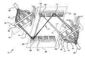
- FIG. 1is a diagrammatic representation of the Optical Cross Connect Switch of the present invention showing the three (3) basic components, including a beam generating portion, beam directing portion, and beam receiving portion;
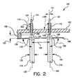
- FIG. 2is a cross-sectional view of the beam generating portion of the Optical Cross Connect Switch of the present invention showing the input fiber and its associated lenslet which generate a communication beam, and the alignment fiber and its associated lenslet which generate an alignment beam;
- FIG. 3is a side view of the beam directing portion of the Optical Cross Connect Switch of the present invention showing the first beam director, second beam director, and the communication beam and alignment beam as they propagate between the first beam director and second beam director;
- FIG. 4is a cross-sectional view of the beam receiving portion of the Optical Cross Connect Switch of the present invention showing the communication beam which is directed to its output fiber through its associated lenslet, and the alignment beam which is directed to the alignment sensor through its associated lenslet;
- FIG. 5is a perspective view of the beam receiving portion of the Optical Cross Connect Switch of the present invention showing the relationship between the position of the communication beam on the output fiber and the alignment beam on the alignment sensor;
- FIG. 6is a block diagram of the control system of the Optical Cross Connect Switch of the present invention showing the computer control of the beam directing portion and its associated optical feedback;
- FIG. 7is a diagrammatic representation of an alternative embodiment of the Optical Cross Connect Switch of the present invention showing the three (3) basic components, including a beam generating portion, beam directing portion, and beam receiving portion;
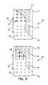
- FIG. 8is a plan view of an alternative architecture for the beam generating portion and beam receiving portion of the Optical Cross Connect Switch of the present invention with parts cut away for clarity;
- FIG. 9is a plan view of another alternative architecture for the beam generating portion and beam receiving portion of the Optical Cross Connect Switch of the present invention with parts cut away for clarity;
- FIG. 10is a partial cross-sectional view of the beam receiving portion of the Optical Cross Connect Switch of the present invention showing the positioning of the output fiber through a fiber alignment hole in the substrate;
- FIG. 11is an exploded view of an alignment beam light source including a light emitting diode (LED) and a mask which allows only a portion of the light generated from the LED to be emitted for creating an alignment beam; and
- LEDlight emitting diode
- FIG. 12is a side view of the alignment beam light source of FIG. 11, showing the creation of a diverging light beam.
- Switch 50includes three (3) basic components, including a beam generating portion 100 , a beam directing portion 200 , and a beam receiving portion 300 .
- Beam generating portion 100includes a substrate, or platform, 102 which receives a number of optical fibers 104 leading from a bundle 106 of optical fibers 104 .
- a lenslet panel 108is positioned adjacent substrate 102 and is formed with an array of communication lenslets 110 for creating a number of communications beams 114 , and an array of alignment lenslets 112 for creating a number of alignment beams 116 .
- Beam generating portion 100is configured with the input fibers 104 being placed in a two-dimensional array.
- the array shown in FIG. 1is a 4 ⁇ 4 array corresponding to sixteen (16) communication beams.
- Beam directing portion 200includes a first beam director 202 and a second beam director 204 , with each director 202 and 204 having an array of beam-directing elements 206 , 208 , 210 , and 212 .
- these beam-directing elementsinclude micro electromechanical systems (MEMS) devices.
- MEMSmicro electromechanical systems
- Beam receiving portion 300includes a substrate 302 which receives a number of output fibers 304 from a fiber bundle 306 .
- Adjacent substrate 302is a lenslet panel 308 which is formed with an array of communication lenslets 310 for receiving the communication beam 114 , and an array of alignment lenslets 312 for focusing the alignment beam 116 onto a portion of the substrate 302 .
- the operation of the Optical Cross Connect Switch of the present invention 50includes the generation of a communication beam 114 and its associated alignment beam 116 in the beam generation portion 100 . As shown these beams 114 and 116 are directed to a beam directing element 208 on first beam director 202 of the beam directing portion 200 , which are then directed to a second beam directing element 212 on second beam director 204 . From second beam directing element 212 , both the communication beam 114 and its associated alignment beam 116 are directed to beam receiving portion 300 where the beams 114 and 116 strike lenslets 310 and 312 , respectively.
- the size and configuration of the array of beam directing elements 206 and 208 on first substrate 202corresponds to the size and configuration of the beam generating portion 100 .
- the configurationis a 4 ⁇ 4 array.
- the present inventionmay be scaled to any size configuration, without any significant increase in complexity of the manufacturing, alignment, or corresponding control system.
- the communication beam 114 and corresponding alignment beam 116are generated by the lowermost and leftmost lenslets 110 and 112 of beam generation portion 100 . These beams 114 and 116 then propagate directly to the beam directing element 208 on first substrate 202 in beam directing portion 200 . Importantly, there is a direct correlation between the particular communication beam generating lenslet 112 and beam directing element 208 . In other words, each of the communication beams 114 and its associated alignment beams 116 propagate to a unique beam directing element 208 .
- each communication lenslet 310 and its corresponding alignment beam lenslet 312 in beam receiving portion 300correspond to a single beam directing element 212 in second substrate 204 of beam directing portion 204 . Again, there is a direct correlation between the particular communication beam receiving lenslet 310 and beam directing element 212 .
- the selective switching of the communication beam 114 from one input fiber 104 to an output fiber 304occurs in the selective positioning of beam directing elements 208 and 212 . More specifically, because each input fiber 104 is associated with its own unique communication beam lenslet 110 which generates communication beam 114 , and each output fiber 304 is associated with its own unique communication beam lenslet 310 which receives communication beam 114 , then the selective switching of a communication beam between the input fiber 104 and the output fiber 304 occurs between first substrate 202 and second substrate 204 in beam directing portion 200 .
- FIG. 1also includes a communication beam 115 (shown in dashed lines) and an alignment beam 117 (shown in dashed lines). These beams 115 and 117 represent an alternative switching position for beam directing portion 200 .
- first beam direction element 208 on first substrate 202directs the communication beam 115 and alignment beam 117 to second beam direction element 209 on second substrate 204 which in turn directs beams 115 and 117 to communication beam lenslet 311 and alignment lenslet 313 , respectively.
- communication and alignment lenslets 311 and 313correspond to beam directing element 209 in second substrate 204 .
- a communication beam 114 from any input fiber 104may be directed to any output fiber 304 . More specifically, by changing the orientation of the appropriate beam directing element in the first substrate 202 corresponding to the input fiber 104 , to direct the communication and alignment beams to any one of the beam directing elements in the second substrate 204 corresponding to the output fiber 304 .
- communication beam 114 and alignment beam 116converge slightly from lenslet panel 108 such that the beams 114 and 116 intersect at location 214 , approximately half of the optical beam path of the Optical Cross Connect Switch 50 .
- the benefits of this slight convergence, and alternatives to such convergence,are discussed more fully in conjunction with FIG. 3 .
- Beam generating portion 100includes a substrate 102 formed with a number of fiber alignment holes 103 that receive fibers 104 from bundle 106 (not shown in this Figure).
- Lenslet panel 108is substantially parallel and spaced apart from substrate 102 , and help rigidly in place.
- lenslet panel 108is secured to substrate 102 with spacers 109 , but any other manner of maintaining the relative positions between substrate 102 and lenslet panel 108 may be used.
- each fibermay be inserted into a ferrule 118 .
- Typical ferruleshave precise dimensions which are known, and thus, the location of input fiber 104 may be determined to a high degree of accuracy.
- substrate 102is made from a dimensionally stable material, including silicon, ceramic or alumina, for example. This material provides for the precision formation of fiber alignment holes 103 using laser drilling techniques. This provides a substantially smooth wall for fiber alignment hole 103 which facilitates the proper positioning of fibers 104 .
- lenslet panel 108is equipped with an array of lenslets 110 and 112 for generating a separate and autonomous communication beam 114 and an alignment, or guidance, beam 116 .
- the end 120 of input fiber 104extends slightly from ferrule 118 and generates a diverging light source 124 (shown in dashed lines).
- Lenslet 110is separated from end 120 by a distance 122 which, in a preferred embodiment, is approximately the focal length of the lenslet 110 .
- lenslet 110receives substantially all light from input fiber 104 and generates communication beam 114 , that is substantially collimated, and has a diameter 130 .
- the angle 125 between input fiber 104 and substrate 102contributes to the communication beam angle 126 .
- this angle 125may be ninety degrees (90°), resulting in a communication beam angle 126 of ninety degrees (90°) and propagating along optical axis 128 .
- Substrate 102also receives a light source for generating alignment beam 116 .
- a light supplying fiber 140is received in ferrule 142 and positioned at an angle 144 to substrate 102 .
- fiber 140provides a diverging light source 148 (shown in dashed lines) which strikes lenslet 112 to create alignment beam 116 .
- the angle 150 of the optical axis 152 of alignment beam 116may vary as a result of the angle 144 of light supplying fiber 140 .
- Angle 150may also be changed by varying the placement of light supplying fiber 140 relative to lenslet 112 . More specifically, by positioning light supplying fiber 140 in direction 141 , the diverging light source 148 strikes lenslet 112 off of the optical axis. As is well known in the art, this off-axis position creates an angle 150 of alignment beam 116 . While two separate methods for directing alignment beam 116 have been discussed, it should be appreciated that any manner of directing alignment beam 116 at an angle 150 known in the art are fully contemplated herein.
- Angle 126 of communication beam 114 and angle 150 of alignment beam 116may be varied by changing the angles 125 and 144 of the fibers 104 and 140 , respectively. Thus, although beams 114 and 116 are separated by a distance 156 , these beams may converge, diverge or remain parallel.
- Beam directing portion 200includes a first beam director 202 and a second beam director 204 , each formed with a number of beam directing elements 206 , 208 , 209 , 212 , for example.
- beam directing elementsinclude a micro electromechanical system, also referred to as a MEMS device.
- MEMS devicesare manufactured of silicon using techniques similar to those techniques for manufacturing semiconductor devices.
- MEMS devicescan vary the orientation of its substantially planar reflective surface by varying the voltages applied to the device.
- the reflective surfacemay be rotated about two (2) axes, where the axes are orthogonal.
- each of the beam directing elements 206 , 208 , 209 , 212are constructed to pivot about two axis. More specifically, beam directing element 208 in first beam director 202 has a first axis of rotation 216 which allows for the rotation of the element in direction 218 , and a second axis of rotation 220 which allows for rotation of the element in direction 222 . Similarly, beam directing element 212 in second beam director 204 has a first axis of rotation 230 which allows for rotation of the element 212 in direction 232 , and a second axis of rotation 234 which allows for rotation of the element 212 in direction 236 . Preferably, axes 216 and 220 are perpendicular, and axes 230 and 234 are perpendicular, however, non-perpendicular orientations are also contemplated, and fully within the scope of the present invention.
- communication beam 114 and alignment beam 116propagate from beam generating portion 100 to strike beam directing element 208 within beam directing portion 200 . Since beam directing element 208 may be rotated about axes 216 and 220 , the communication beam 114 and alignment beam 116 may be redirected to any beam directing element on second beam director 204 simply by rotating about its axes. Thus, as discussed above in conjunction with FIG. 1, communication beam 114 and alignment beam 116 may be directed to any beam directing element on second beam director 204 , which in turn directs the beams to its associated output fiber 304 in beam receiving portion 300 .
- Beam receiving portion 300includes a substrate 302 formed with an fiber alignment hole 303 that receives an output fiber 304 .
- Lenslet panel 308contains lenslets 310 and 312 , and which receive communication beam 114 and alignment beam 116 , respectively.
- lenslet panel 308is held substantially parallel to substrate 302 , such as with spacers (not shown this Figure).
- Optical fiber 304may be held in place through substrate 302 with a ferrule 322 .
- the end 320 of fiber 304is retained in place a distance 318 from lenslet 310 .
- distance 318is equal to the focal length of lenslet 310 such that the communication beam 314 passes through lenslet 310 and converges onto end 320 (as shown by the light pattern 316 ).
- Alignment beam 116strikes lenslet 312 and is focussed into a converging light pattern 334 (shown in dashed lines) that converges onto sensor 336 on substrate 302 .
- the focal length of lenslet 312is equal to distance 338 such that the alignment beam is focussed onto the surface of the sensor 336 .
- the focal length of lenslet 312may be greater or less than distance 338 .
- lenslet 310may be omitted entirely from the lenslet panel 308 allowing alignment beam 116 to strike sensor 336 .
- the communication beam 114 and alignment beam 116converge slightly such that the two beams intersect at the approximate midpoint of the optical pathway between the beam generating portion 100 and the beam receiving portion 300 .
- the distance 224 between the contact points on the beam directing element 208is minimized.
- the physical dimensions of each beam directing element 208may be minimized which in turn allows for a smaller beam directing portion 200 .
- the distance 156 between the input fiber 104 and alignment light source 140 , and the distance 332 between the output fiber 304 and the center of the sensor 336are approximately equal. This equality is useful in the initial positioning the beam directing elements, as will be discussed in greater detail below.
- the beamsmay be positioned such that they are substantially parallel.
- the angle of incidence of the communication beam 114 on the beam directing elements 208 and 212is identical to the angle of incidence of the alignment beam 116 on the same beam directing elements. Consequently, there is a direct correlation between the distance 156 between the communication beam 114 and the alignment beam 116 in the beam generation portion 100 , and the distance 332 between the communication beam 114 and the alignment beam 116 in the beam receiving portion 300 . In fact, in some instances, distances 156 and 332 will be the same, which provides for the initial positioning of the beam directing elements.
- FIGS. 1, 2 , 3 , and 4have shown communication beam 114 and alignment beam 116 having diameters 130 and 154 , respectively, it is to be appreciated that these graphical representations are for discussion purposes, and that the relative sizes and proportions shown in these figures is not to be considered as any limitation whatsoever of the present invention. Rather, it is to be appreciated that the diameters 130 and 154 of the beams 114 and 116 may be greater or smaller, and that the sizes of the lenslets 110 and 112 may also be smaller or larger. Also, distances 156 and 332 may also be smaller or larger, depending on the particular design of the present invention.
- FIG. 5a perspective view of the beam receiving portion 300 of the Optical Cross Connect Switch 50 of the present invention is shown and illustrates the relationship between the output fiber 304 , the sensor 336 , and the communication and alignment beams 114 , 116 .
- lenslet panel 308contains lenslet 310 which receives communication beam 114 and generates a converging pattern 316 .
- This converging pattern 316converges onto output fiber 304 which extends through ferrule 322 and substrate 302 .
- the converging pattern 316must converge onto the core 321 of the output fiber 304 .
- the diameter of the core 321 in a typical single mode (SM) optical fiberis approximately seven micrometers (7 ⁇ m). Consequently, there is very little tolerance for mis-alignment between the converging pattern 316 and the core 321 at end 320 of output fiber 304 .
- SMsingle mode
- a position sensor 336is provided to detect the position of alignment beam 116 .
- Alignment beam 116passes through lenslet 312 into focussing light pattern 334 which strikes sensor 336 .
- the relationship between the position of the communication beam 114 on the output fiber 304 and the alignment beam 116 on the alignment sensor 336is known.
- the focussing light pattern 316 from the communication beam 114strikes the end 120 of fiber 104 at a location offset from where the focusing light pattern 334 of the alignment beam 116 strikes the sensor 336 .
- This offsetcan be characterized is a combination of an X-offset 350 and a Y-offset 352 .
- the particular offset values 350 and 352 for each combination of beam directing elementsare known. These values may be determined mathematically using the particular physical components of the system 50 , including the convergence angles 126 and 150 of the communication beam 114 and the alignment beam 116 , the rotational position of the beam directing elements in directions 218 , 222 , 232 , and 236 , and the optical path length. Alternatively, the offset values may be measured by constructing or modeling the device 50 and measuring the offset values 350 and 352 for each combination of beam director elements.
- the focusing light pattern 316may be precisely positioned on core 321 of fiber 104 by adjusting the rotational positions of the beam director elements 208 and 212 to position the alignment beam at the precise location 337 identified by distance 354 and 356 on sensor 336 .
- the alignment beam 116is properly positioned at location 337 within sensor 336 according to the particular offset values 350 and 352 , the converging light pattern 334 from communication beam 114 will likewise be properly positioned directly on core 321 on the end 320 of fiber 304 .
- Sensor 336is a light-sensitive sensor which provides an output signal corresponding to the location where the alignment beam focusses on the sensor.
- a variety of suitable sensorscould be fabricated using known technologies, including those technologies used in manufacturing an array of position sensitive diodes (PSD), a charge coupled device (CCD) panel, and a light sensitive CMOS array.
- the PSD sensorprovides a pair of analog voltages which correspond to the location where a light beam strikes the sensor.
- sensor 336would provide two (2) separate analog voltages corresponding to the location 337 on sensor 336 where focussed light beam 336 strikes the sensor, with a first analog voltage corresponding to the distance 354 , and a second analog voltage corresponding to the distance 356 . These analog voltages may be measured to determine whether the converging light pattern 334 of alignment beam 116 is in the proper position given the particular beam directors 208 and 209 which are being used.
- the beam directorsmay be adjusted to further position the communication and alignment beams 114 and 116 .
- the beam directorsmay be adjusted to move both the communication beam 114 and alignment beam 116 in directions 362 and 360 , respectively.
- beam directorsmay be adjusted to move both the communication beam 114 and alignment beam 116 in directions 366 and 364 , respectively.
- a CMOS pixel arraymay be used to precisely locate the converging beam 334 on sensor 36 .
- a CMOS arrayprovides a two (2) dimensional array of pixels 344 which precisely image the converging light beam 334 . This image may be analyzed to identify distances 354 and 356 to determine the location of alignment beam 116 . Then, as described above, if distances 354 and 356 do not correspond to the position 337 where converging light beam 316 from communication beam 114 focusses onto core 321 of output fiber 304 , beam directors may be adjusted in order to move communication beam 114 and corresponding alignment beam 116 in directions 362 and 360 , and 366 and 364 , or a combination of those directions.
- directions 360 , 362 , 364 and 366have been depicted in FIG. 5 as positive, it is to be appreciated that these directions are merely exemplary of movement of the communication beam 114 and corresponding alignment beam 116 on lenslets 310 and 312 . This movement may be any direction, thus accommodating any location 337 where converging beam 334 strikes sensor 336 .
- the location 337 of the alignment beam 334can be determined in one of several manners. For example, a standard centroid calculation may be used.
- the sensorconsists of an array of light sensitive pixels and the location of the “spot” is calculated by dividing the weighted sum of the measured pixel intensities by the total measured intensity of the beam. This, in effect, computes an intensity center of gravity which corresponds to the location of the center of the beam.
- Other, more advanced techniques for determining the location of the beammay also be used.
- Control system 400includes a computer 402 containing a real time computer 404 , a telecommunications interface 406 , and a digital storage device 408 .
- Computer 402is a system capable of making the computations required to implement a closed-loop feedback control system. It may be comprised of analog or digital electronics, or may be implemented with optical computations units. In a preferred embodiment, the computer consists of digital electronics with at least one component capable of computation, and with at least three digital interfaces. The first interface would be capable of receiving the digitized optical feedback signals, the second interface would be capable of transmitting command signals to the analog electronic driver required for actuation of beam directors 202 and 204 . And the third interface would be capable of receiving the network configuration command from an external source and transmitting the state of the optical switch. Other interfaces may be required for certain implementations.
- the digital computation electronicscould consist of one or more general purpose processors, such as a commercial available digital signal processor (DSP) or other central processing unit (CPU), or might be on e or more application specific integrated circuits (ASIC) design specifically for this task.
- DSPdigital signal processor
- CPUcentral processing unit
- ASICapplication specific integrated circuits
- the digital interfacescould consist of any one of a large variety of parallel or serial links and may conform to some industry standards, or may be custom for a particular implementation.
- Telecommunication interface 406provides an electronic interface between computer 402 and a telecommunication exchange via interconnect 410 .
- interconnect 410will receive switching information, including the input fibers 104 and the output fibers 304 , which are to be optically coupled.
- a standard format for receiving this informationmay be established by a particular telecommunications network, but it is to be appreciated that regardless of the particular protocol, this information will contain particular switch configurations which may be implemented by the present invention.
- Digital storage device 408may include both temporary and permanent digital memory media.
- digital storage device 408may include random access memory (RAM) for manipulation of data, and programmable read only memory (PROM) for storage of programed computer sequence steps, and may include tables of offset values.
- RAMrandom access memory
- PROMprogrammable read only memory
- Computer 402is electrically connected to digital interface 414 via electrical connection 416 .
- Digital interface 414contains high voltage amplifiers, and digital to analog converters (DACs) that convert digital information from computer 402 to the analog signals necessary to control the beam director elements ( 208 and 212 in FIG. 3 ), such as MEMS devices.
- Digital interface 414also transmits and receives any necessary digital data between computer 402 and beam directors 418 .
- Beam directors 418 and 419receive the electronic signals from interface 414 which drive each of the beam directing elements 420 to their particular rotational position in order to direct communication beam 114 from one input fiber 104 to its intended output fiber 304 .
- optical sensor 422measures the position of the alignment beam, depicted in FIG. 6 as optical feedback 421 . Specifically, optical sensor 422 measures the position of the alignment beam 116 within the sensor area 336 , and provides that position information electronically via electrical connection 424 to analog interface 426 .
- Analog interface 426contains analog signal conditioning components, including analog amplifiers and analog to digital converters (ADCs), which receive the analog signals from optical sensor 422 and generate digital signals for transmission along electrical connection 428 to computer 402 .
- analog signal conditioning componentsincluding analog amplifiers and analog to digital converters (ADCs), which receive the analog signals from optical sensor 422 and generate digital signals for transmission along electrical connection 428 to computer 402 .
- ADCsanalog to digital converters
- Computer 402receives the electronic information from sensor 422 regarding the position of the alignment beam, and compares this position to the position contained in the memory 408 to determine whether the beam director elements 420 in beam directors 418 and 419 are properly positioned. If there is a difference between the position of the alignment beam measured by sensor 422 and the position data contained in memory 408 , computer 402 adjusts the electronic signals sent to digital interface 414 to modify the rotational position of beam director elements 420 and re-position the alignment beam within the sensor. The position of the alignment beam is then once again measured by optical sensor 422 , and the adjustment to the rotational positions of the beam directing elements is repeated if necessary. By properly positioning the alignment beam in this manner, the proper position of the communication beam is achieved without any interference with or measurement of the communication beam itself.
- the Optical Cross Connect Switch 50 of the present inventiontransmits an optical signal from an input fiber 104 to an output fiber 304 .
- the operation of a preferred embodiment of the present inventionis perhaps best understood with reference to FIGS. 1, 3 , and 5 .
- the guidance and control systemincorporates a single un-modulated DC optical guidance beam for each input fiber.
- the communications beam and its companion guidance beamboth pass through a micro-lens array, labeled 100 in the figure, which transform the diverging beams into nearly collimated beams.
- the microlens arrayhas a separate micro lens for each communication beam 110 , and a separate one for each guidance beam 112 .
- the communication and guidance beam pairAfter passing through the micro lens array, the communication and guidance beam pair are nearly parallel, but are purposefully misaligned slightly so that the beams cross near the center of the free space optical path.
- the communication-guidance beam pairencounter a second micro lens array which focusses the two beams.
- the communication beamis focussed onto a single output fiber and the guidance beam is focussed on a CMOS sensor.
- each beam steering elementis positioned in its nominal flat position parallel with the plan of the gird of mirror elements as defied by element 202 in FIG. 1 .
- the communications-alignment beam pairsare positioned without optical feedback, and the switch is configured such that each alignment beam falls on the sensor corresponding to the nominal straight path or non-switched output fiber.
- Closed-loop feedbackis then initiated on all of the communications-guidance beam pairs, and residual open-loop pointing errors in the beam steering elements are removed using a servo control loop.
- Reconfiguration of the input-output mapping of fibers, the switch fabricis accomplished as follows.
- the beam steering mirrors of the affected channelsUpon receipt of a reconfiguration command, the beam steering mirrors of the affected channels immediately perform an open loop step, moving from their current position to a new position appropriate for completing the commanded reconfiguration.
- control feedbackis terminated on the affected channels.
- the beam steering elementWhen the beam steering element are near their new positions, the guidance beam falls on the portion of the sensor correspond to the new output fiber indicated by the configuration command.
- closed loop servo controlis re-initiated and the new connection is finalized.
- the guidance beam for the repositioning channelsmay be switched off in order to eliminate any contamination of the servo feedback signal of non-switched channels by the guidance beams of the switching channels.
- the control algorithmcan be designed to ignore any effects of stray guidance light from the switching channels, which may arise while scanning those beams during their open-loop step, and which might reach the sensors of those channels not switching.
- the servo loopmay operate only on the mirror elements in the second mirror array. In alternative embodiments, the servo loop may operate on the mirror elements in the first mirror array, the second mirror array, or both the first and second mirror arrays.
- the calibration of each of the mirror elements in the first arrayis sufficiently accurate that it is possible to position these elements with an open loop signal such that substantially all of the optical energy of the alignment and communications beams corresponding to each element will fall on the intended target mirror element in the second beam director array.
- the open loop pointing of the beam directing mirror elementsis calibrated at manufacture, and periodically throughout the lifetime of the device, insuring that the open loop pointing accuracy is high. Also, the open loop pointing accuracy of the mirrors in the first array needs to be no better than a few percent of the full stroke since small errors in position of the first elements are, in effect compensated by the closed loop servo control system operating on elements in the second mirror array. This initial open loop pointing, in combination of the feedback control of the second beam directing elements accurately positions the communication beam onto the center of the output fiber.
- Switch 500includes a beam generating portion 502 , a beam directing portion 504 , and a beam receiving portion 506 .
- Beam generating portion 502is an equivalent to beam generating portion 100 and beam receiving portion 506 is an equivalent to beam receiving portion 300 shown, as shown in FIG. 1 .
- Beam directing portion 504includes a first beam director 530 and a second beam director 534 , with each director 530 and 534 having an array of beam-directing elements 536 , 538 , 540 and 542 .
- these beam-directing elementsmay include micro electromechanical systems (MEMS) devices, or other beam directing elements known in the art.
- Beam directing portion 504also includes a reflector 532 which has a reflective surface 533 .
- a communication beam 522 and an alignment beam 524are generated in beam generating portion 502 and propagate into beam directing portion 504 , striking a beam directing element 536 in first beam director 530 corresponding to the lenslets 518 and 520 .
- Beam directing element 536re-directs communication beam 522 and alignment beam 524 to a beam directing element in second beam director 534 , such as beam directing element 540 .
- the re-directing of communication and alignment beams 522 and 524is accomplished by reflecting these beams from reflector 532 . From beam director element 540 , the communication and alignment beams 522 and 524 are directed to lenslets 572 and 574 .
- the communication beam 522 and alignment beam 524may converge, and may intersect midway along the optical pathway through switch 500 . In the present embodiment, such intersection may occur at approximately location 544 .
- beam generating portion 600generates a communication beam and an alignment beam which propagate through the beam directing portion 200 .
- beam receiving portion 650receives a communication beam into an output fiber, and an alignment beam into a position sensor.
- an alternative embodiment beam generating portion 600which includes a substrate 602 formed with an array of fiber alignment holes 604 for receiving an optical fiber and associated ferrule (not shown this Figure).
- An alignment beam generator 606is either mounted to the surface of, or made integral to, substrate 602 , and may include an optical fiber with an associated ferrule as described in conjunction with FIG. 2 .
- alignment beam generatormay include a light emitting diode (LED) 608 which emits light that is directed away from substrate 602 . This light direction may be accomplished by providing a mask 610 over LED 608 .
- mask 610is formed with a small hole 611 which allows only a small portion of the light generated by LED 608 to pass through the mask in the form of a diverging light beam.
- the diverging light beam from LED 608passes through a lenslet, on panel 612 , such as lenslet 614 , to create an alignment beam (not shown this Figure).
- Light emitted from the input fiber in fiber alignment hole 604passes through a lenslet, such as lenslet 616 , on panel 612 to create a communication beam (not shown this Figure).
- Beam receiving portion 650includes a substrate 652 which is formed with an array of fiber alignment holes 654 for receiving an output fiber supported by its associated ferrule (not shown this Figure). Substrate 652 is also formed with an array of sensors 656 which may be formed integral to, or attached to the surface of, substrate 652 . Panel 658 includes an array of lenslets 660 which are positioned above fiber alignment holes 654 containing output fibers, and an array of lenslets 662 which are positioned above sensors 656 .
- the distance 618 between fiber alignment holes 604 which contain the input fibers and their associated ferrulesis substantially equal to distance 664 between fiber alignment holes 654 which contain output fibers and their associated ferrules.
- This spacingprovides for a consistent spacing between output fibers and sensors 656 , and facilitates the directing of the communication and alignment beams through the beam directing portion 300 .
- FIG. 9is a plan view of another alternative architecture for the beam generating portion 100 and beam receiving portion 300 of the Optical Cross Connect Switch 650 of the present invention.
- Beam generating portion 700generates a communication beam and an alignment beam which propagate through the beam directing portion 200 . Further, like beam receiving portion 300 , beam receiving portion 750 receives a communication beam into an output fiber, and an alignment beam into a position sensor.
- Beam generating portion 700includes an alignment beam generator 706 is either mounted to the surface of, or made integral to, substrate 702 , and includes a light emitting diode (LED) 708 which emits light that is directed away from substrate 702 .
- the diverging light beam from LED 708passes through a lenslet, on panel 712 , such as lenslet 714 , to create an alignment beam (not shown this Figure).
- Light emitted from the input fiber in fiber alignment hole 704passes through a lenslet, such as lenslet 716 , on panel 712 to create a communication beam (not shown this Figure).
- Beam receiving portion 750includes a substrate 752 which is formed with an array of fiber alignment holes 754 for receiving an output fiber supported by its associated ferrule (not shown this Figure). Substrate 752 is also formed with an array of sensors 756 which may be formed integral to, or attached to the surface of, substrate 752 . Panel 758 includes an array of lenslets 760 which are positioned above fiber alignment holes 754 containing output fibers, and an array of lenslets 762 which are positioned above sensors 756 .
- FIG. 10a partial cross-sectional view of the beam receiving portion of the Optical Cross Connect Switch of the present invention is shown and generally designated 800 .
- the substrate 802is shown with an fiber alignment hole 804 .
- a ferrule 806Spaced behind substrate 802 is a ferrule 806 which receives an optical fiber 808 having an end 810 which extends through substrate 802 and contacts inner wall 812 of fiber alignment hole 804 .
- ferrule 806may be positioned away from substrate 802 a distance 816 , the contact between end 810 of fiber 808 and inner wall 812 of fiber alignment hole 804 provides a positive position force on fiber 810 which stabilizes the position of the fiber 804 so that a communication beam may be focussed onto end 810 .
- This same constructionmay be implemented in a beam generating portion to provide the proper positioning of an input fiber, such as fiber 104 , for the generation of communication or alignment beams 114 or 116 .
- Alignment beam generator 606includes a base 609 containing an LED 608 having a light emitting area 607 .
- Mask 610is formed with a small hole 611 having a diameter 620 which allows only a small portion of the light generated by LED 608 to propagate from the mask in the form of a diverging light beam 148 .
- Diameter 620is much less than diameter 622 of light emitting area 607 which provides for a strong, yet localized, source of light for creating diverging light beam 148 .
Landscapes
- Physics & Mathematics (AREA)
- General Physics & Mathematics (AREA)
- Optics & Photonics (AREA)
- Mechanical Light Control Or Optical Switches (AREA)
- Optical Couplings Of Light Guides (AREA)
Abstract
Description
Claims (39)
Priority Applications (5)
| Application Number | Priority Date | Filing Date | Title |
|---|---|---|---|
| US09/846,879US6731833B2 (en) | 2001-01-16 | 2001-04-30 | Optical cross connect switch |
| US09/960,223US6968098B2 (en) | 2001-01-16 | 2001-09-20 | Method for providing variable optical attenuation |
| US09/960,616US6614982B2 (en) | 2001-01-16 | 2001-09-20 | Variable optical attenuator |
| PCT/US2002/005285WO2002067027A1 (en) | 2001-01-16 | 2002-01-16 | Optical cross connect switch |
| US10/838,070US7050669B2 (en) | 2001-04-30 | 2004-05-03 | Optical cross connect switch with axial alignment beam |
Applications Claiming Priority (3)
| Application Number | Priority Date | Filing Date | Title |
|---|---|---|---|
| US26226201P | 2001-01-16 | 2001-01-16 | |
| US27343301P | 2001-03-05 | 2001-03-05 | |
| US09/846,879US6731833B2 (en) | 2001-01-16 | 2001-04-30 | Optical cross connect switch |
Related Parent Applications (1)
| Application Number | Title | Priority Date | Filing Date |
|---|---|---|---|
| US09/960,225Continuation-In-PartUS20020122616A1 (en) | 2001-03-05 | 2001-09-20 | Optical beacon for aligning mirror systems |
Related Child Applications (3)
| Application Number | Title | Priority Date | Filing Date |
|---|---|---|---|
| US09/960,223Continuation-In-PartUS6968098B2 (en) | 2001-01-16 | 2001-09-20 | Method for providing variable optical attenuation |
| US09/960,616Continuation-In-PartUS6614982B2 (en) | 2001-01-16 | 2001-09-20 | Variable optical attenuator |
| US10/838,070Continuation-In-PartUS7050669B2 (en) | 2001-04-30 | 2004-05-03 | Optical cross connect switch with axial alignment beam |
Publications (2)
| Publication Number | Publication Date |
|---|---|
| US20020122619A1 US20020122619A1 (en) | 2002-09-05 |
| US6731833B2true US6731833B2 (en) | 2004-05-04 |
Family
ID=27401497
Family Applications (3)
| Application Number | Title | Priority Date | Filing Date |
|---|---|---|---|
| US09/846,879Expired - LifetimeUS6731833B2 (en) | 2001-01-16 | 2001-04-30 | Optical cross connect switch |
| US09/960,616Expired - LifetimeUS6614982B2 (en) | 2001-01-16 | 2001-09-20 | Variable optical attenuator |
| US09/960,223Expired - LifetimeUS6968098B2 (en) | 2001-01-16 | 2001-09-20 | Method for providing variable optical attenuation |
Family Applications After (2)
| Application Number | Title | Priority Date | Filing Date |
|---|---|---|---|
| US09/960,616Expired - LifetimeUS6614982B2 (en) | 2001-01-16 | 2001-09-20 | Variable optical attenuator |
| US09/960,223Expired - LifetimeUS6968098B2 (en) | 2001-01-16 | 2001-09-20 | Method for providing variable optical attenuation |
Country Status (2)
| Country | Link |
|---|---|
| US (3) | US6731833B2 (en) |
| WO (1) | WO2002067027A1 (en) |
Cited By (13)
| Publication number | Priority date | Publication date | Assignee | Title |
|---|---|---|---|---|
| US20020176657A1 (en)* | 2001-03-19 | 2002-11-28 | Elliot Burke | Beam convergence system for optical switching cores |
| US20040047547A1 (en)* | 2002-09-10 | 2004-03-11 | Yakov Reznichenko | Two input, two output optical switch using two movable mirrors |
| US20040190816A1 (en)* | 2002-08-20 | 2004-09-30 | Fujitsu Limited | Optical switch and using method therefor |
| US20040208468A1 (en)* | 2001-10-24 | 2004-10-21 | Zbigniew Sufleta | Variable optical attenuator |
| US20050031255A1 (en)* | 2003-08-07 | 2005-02-10 | Schroeder Dale W. | Method and system for maintaining active alignment in an optical switch using dedicated representative directing elements |
| US20050117837A1 (en)* | 2001-08-28 | 2005-06-02 | Ugo Cerato | Optical switching device for wavelength division multiplex (WDM) telecommunications network |
| US6978061B1 (en)* | 2004-10-08 | 2005-12-20 | Fujitsu Limited | Optical switching device |
| US20170075074A1 (en)* | 2014-05-27 | 2017-03-16 | Huawei Technologies Co., Ltd. | Optical Switch and Wavelength Division Multiplexing Optical System |
| US20190081703A1 (en)* | 2017-09-14 | 2019-03-14 | Facebook, Inc. | Compact system for active co-boresight measurement in a laser communication system |
| US10317626B2 (en) | 2017-06-15 | 2019-06-11 | Google Llc | Inner and outer collimator elements for an optical circuit switch |
| US11543645B1 (en) | 2020-03-19 | 2023-01-03 | Meta Platforms, Inc. | Optical beam expander with partial monolithic structure |
| US11546062B1 (en) | 2020-04-22 | 2023-01-03 | Meta Platforms, Inc. | Wavelength-selectable free-space optical communication |
| US11689283B1 (en) | 2020-03-30 | 2023-06-27 | Meta Platforms, Inc. | Free-space optical communication system using a backchannel for power optimization |
Families Citing this family (30)
| Publication number | Priority date | Publication date | Assignee | Title |
|---|---|---|---|---|
| US6618520B2 (en)* | 1999-11-09 | 2003-09-09 | Texas Instruments Incorporated | Micromirror optical switch |
| US6731833B2 (en)* | 2001-01-16 | 2004-05-04 | T-Rex Enterprises Corp. | Optical cross connect switch |
| WO2002101432A2 (en)* | 2001-01-17 | 2002-12-19 | Corning Incorporated | Optical switch with time multiplexing control system architecture |
| US6834138B2 (en)* | 2001-03-06 | 2004-12-21 | Corning Incorporated | Modular optical switch fabric |
| JP3889247B2 (en)* | 2001-03-15 | 2007-03-07 | 日本板硝子株式会社 | Optical module and method for assembling the same |
| US6819824B1 (en)* | 2001-05-21 | 2004-11-16 | Calient Networks | Optical switch package |
| US6680776B2 (en)* | 2001-09-20 | 2004-01-20 | Trex Enterprises Corp. | Method and apparatus for sensing a power level of a communications beam in a fiber optic switch |
| US6640023B2 (en)* | 2001-09-27 | 2003-10-28 | Memx, Inc. | Single chip optical cross connect |
| US6794793B2 (en)* | 2001-09-27 | 2004-09-21 | Memx, Inc. | Microelectromechnical system for tilting a platform |
| US6766085B2 (en)* | 2001-10-01 | 2004-07-20 | Agilent Technologies, Inc. | Precisely configuring optical fibers and other optical elements using an apertured wafer positioner |
| US7298555B2 (en)* | 2001-12-07 | 2007-11-20 | The Boeing Company | Optical beam steering using small angle beam steering device |
| US6944365B2 (en) | 2002-01-03 | 2005-09-13 | Memx, Inc. | Off axis optical signal redirection architectures |
| US6868236B2 (en)* | 2002-07-18 | 2005-03-15 | Terabeam Corporation | Apparatus and method for combining multiple optical beams in a free-space optical communications system |
| US7106973B2 (en)* | 2002-08-13 | 2006-09-12 | Lightpointe Communications, Inc. | Apparatus and method for use in free-space optical communication comprising optically aligned components integrated on circuit boards |
| US7049570B2 (en)* | 2002-09-16 | 2006-05-23 | Avago Technologies, Ltd. | Optical chip coupling system utilizing micromachine adjustable optical elements and a feedback circuit providing the micromachine with a feedback signal correlated to an optical signal parameter |
| US6707961B1 (en)* | 2002-09-23 | 2004-03-16 | Nortel Networks Limited | Optical cross-connect switch with decreased polarization-dependent loss |
| US6931170B2 (en)* | 2002-10-18 | 2005-08-16 | Analog Devices, Inc. | Fiber-attached optical devices with in-plane micromachined mirrors |
| TW580596B (en)* | 2002-12-03 | 2004-03-21 | Delta Electronics Inc | Variable optical attenuator in micro-electro-mechanical systems and method of making the same |
| US20060088242A1 (en)* | 2003-12-31 | 2006-04-27 | Vlad Novotny | Optical switches with uniaxial mirrors |
| US7263253B2 (en)* | 2005-04-11 | 2007-08-28 | Capella Photonics, Inc. | Optimized reconfigurable optical add-drop multiplexer architecture with MEMS-based attenuation or power management |
| US7756368B2 (en)* | 2005-04-11 | 2010-07-13 | Capella Photonics, Inc. | Flex spectrum WSS |
| JP2009003378A (en)* | 2007-06-25 | 2009-01-08 | Fujitsu Ltd | Mirror device and optical switch |
| US7676126B2 (en)* | 2007-12-12 | 2010-03-09 | Jds Uniphase Corporation | Optical device with non-equally spaced output ports |
| US8538229B1 (en)* | 2009-03-13 | 2013-09-17 | Alliance Fiber Optic Products, Inc. | Pluggable variable optical attenuators and methods for making the same |
| KR20120102387A (en)* | 2011-03-08 | 2012-09-18 | 삼성전자주식회사 | Display apparatus and fabrication method of the same |
| DE102013103708A1 (en)* | 2013-04-12 | 2014-10-16 | Reichle & De-Massari Ag | Optical connection device |
| US10481332B2 (en) | 2017-01-23 | 2019-11-19 | Ii-Vi Delaware, Inc. | Free space variable optical attenuator with integrated input/output power monitors |
| CN109946845B (en)* | 2019-04-12 | 2022-08-16 | 武汉大学 | Method for adjusting optical axis of telescope to zenith accurately |
| US12199665B2 (en) | 2020-06-02 | 2025-01-14 | Nippon Telegraph And Telephone Corporation | Optical monitor device |
| WO2025172970A1 (en)* | 2024-02-16 | 2025-08-21 | Bright Silicon Technologies, Inc. | Precision out-of-channel alignment feedback for optical circuit switching |
Citations (64)
| Publication number | Priority date | Publication date | Assignee | Title |
|---|---|---|---|---|
| US5136671A (en) | 1991-08-21 | 1992-08-04 | At&T Bell Laboratories | Optical switch, multiplexer, and demultiplexer |
| US5243672A (en) | 1992-08-04 | 1993-09-07 | At&T Bell Laboratories | Planar waveguide having optimized bend |
| US5301008A (en) | 1991-11-05 | 1994-04-05 | At&T Bell Laboratories | Optical crossbar exchange arrangement |
| US5524153A (en) | 1995-02-10 | 1996-06-04 | Astarte Fiber Networks, Inc. | Optical fiber switching system and method using same |
| US5594820A (en) | 1995-02-08 | 1997-01-14 | Jds Fitel Inc. | Opto-mechanical device having optical element movable by twin flexures |
| US5600742A (en) | 1994-09-30 | 1997-02-04 | Lucent Technologies Inc. | Wavelength grating router with output coupler |
| US5621829A (en) | 1996-04-02 | 1997-04-15 | Lucent Technologies Inc. | Fiber optic switching device and method using free space scanning |
| US5623564A (en) | 1995-06-07 | 1997-04-22 | Lucent Technologies Inc. | Self-aligned mechanical optical switch |
| US5647044A (en) | 1995-12-22 | 1997-07-08 | Lucent Technologies Inc. | Fiber waveguide package with improved alignment means |
| US5654819A (en) | 1994-01-27 | 1997-08-05 | Lucent Technologies Inc. | Micromechanical modulator |
| US5699462A (en) | 1996-06-14 | 1997-12-16 | Hewlett-Packard Company | Total internal reflection optical switches employing thermal activation |
| US5703975A (en) | 1995-06-09 | 1997-12-30 | Corning Incorporated | Interferometric switch |
| US5721796A (en) | 1996-06-21 | 1998-02-24 | Lucent Technologies Inc. | Optical fiber cross connect with active routing for wavelength multiplexing and demultiplexing |
| US5771320A (en) | 1996-04-30 | 1998-06-23 | Wavefront Research, Inc. | Optical switching and routing system |
| US5825517A (en) | 1995-12-06 | 1998-10-20 | Tellium, Inc. | Parametric wavelength interchanging cross-connect |
| US5828800A (en) | 1997-06-23 | 1998-10-27 | Lucent Technologies Inc. | Self-aligned mechanical M×N optical switch |
| US5841917A (en) | 1997-01-31 | 1998-11-24 | Hewlett-Packard Company | Optical cross-connect switch using a pin grid actuator |
| US5841500A (en) | 1997-01-09 | 1998-11-24 | Tellium, Inc. | Wedge-shaped liquid crystal cell |
| US5903687A (en) | 1997-05-02 | 1999-05-11 | Neos Technologies, Inc. | M input port by N output port optical switching system |
| US5923798A (en) | 1997-05-15 | 1999-07-13 | Lucent Technologies, Inc. | Micro machined optical switch |
| US5949571A (en) | 1998-07-30 | 1999-09-07 | Lucent Technologies | Mars optical modulators |
| US5953467A (en) | 1997-09-23 | 1999-09-14 | Lucent Technologies Inc. | Switchable optical filter |
| US5960133A (en) | 1998-01-27 | 1999-09-28 | Tellium, Inc. | Wavelength-selective optical add/drop using tilting micro-mirrors |
| US5963367A (en) | 1997-09-23 | 1999-10-05 | Lucent Technologies, Inc. | Micromechanical xyz stage for use with optical elements |
| US5974207A (en) | 1997-12-23 | 1999-10-26 | Lucent Technologies, Inc. | Article comprising a wavelength-selective add-drop multiplexer |
| US5982515A (en) | 1996-04-30 | 1999-11-09 | Wavefront Research, Inc. | Optical time shifter and routing system |
| US5994159A (en) | 1997-12-22 | 1999-11-30 | Lucent Technologies, Inc. | Self-assemblying micro-mechanical device |
| US5995688A (en) | 1998-06-01 | 1999-11-30 | Lucent Technologies, Inc. | Micro-opto-electromechanical devices and method therefor |
| US6002818A (en) | 1997-12-05 | 1999-12-14 | Lucent Technologies Inc | Free-space optical signal switch arrangement |
| US6005998A (en) | 1998-02-20 | 1999-12-21 | Lucent Technologies Inc. | Strictly non-blocking scalable matrix optical switch |
| US6049640A (en) | 1997-09-04 | 2000-04-11 | Lucent Technologies Inc. | Wavelength-division-multiplexing cross-connect using angular dispersive elements and phase shifters |
| US6067389A (en) | 1998-07-27 | 2000-05-23 | Lucent Technologies Inc. | Wavelength-selective optical cross-connect |
| US6072923A (en) | 1996-04-30 | 2000-06-06 | Wavefront Research, Inc. | Optical switching, routing, and time delay systems using switched mirrors |
| US6075239A (en) | 1997-09-10 | 2000-06-13 | Lucent Technologies, Inc. | Article comprising a light-actuated micromechanical photonic switch |
| US6075512A (en) | 1997-02-05 | 2000-06-13 | Tellium, Inc. | Temperature compensation of a wedge-shaped liquid-crystal cell |
| US6091867A (en) | 1997-05-02 | 2000-07-18 | Neos Technologies, Inc. | M input port by N output port optical switching system |
| US6094246A (en) | 1998-01-06 | 2000-07-25 | Chorum Technologies | Acute twist nematic liquid crystal electro-optic modulator for use in an infrared optical communication system having extinction ratio of -25db |
| US6097860A (en) | 1998-06-05 | 2000-08-01 | Astarte Fiber Networks, Inc. | Compact optical matrix switch with fixed location fibers |
| US6097858A (en) | 1998-06-05 | 2000-08-01 | Astarte Fiber Networks, Inc. | Sensing configuration for fiber optic switch control system |
| US6101299A (en) | 1998-06-05 | 2000-08-08 | Astarte Fiber Networks, Inc. | Optical switch targeting system |
| US6108466A (en) | 1998-09-17 | 2000-08-22 | Lucent Technologies | Micro-machined optical switch with tapered ends |
| US6137941A (en) | 1998-09-03 | 2000-10-24 | Lucent Technologies, Inc. | Variable optical attenuator |
| US6137103A (en) | 1998-07-31 | 2000-10-24 | Lucent Technologies | Opto-mechanical components |
| US6141076A (en) | 1997-11-28 | 2000-10-31 | Chorum Technologies, Inc. | Spatial light modulators constructed from ferroelectric liquid crystal devices with twisted structure |
| US6140737A (en) | 1999-10-08 | 2000-10-31 | Lucent Technologies Inc. | Apparatus and method for charge neutral micro-machine control |
| US6141467A (en) | 1998-03-18 | 2000-10-31 | Lucent Technologies Inc. | Wavelength-division-multiplexing programmable add/drop using interleave-chirped waveguide grating router |
| US6144783A (en) | 1996-07-30 | 2000-11-07 | Nortel Networks Corporation | Optical multiplexter/demultiplexer |
| US6144482A (en) | 1997-11-14 | 2000-11-07 | Neos Technologies, Inc. | Acousto-optic modulator for selective extraction of one or more wavelengths from randomly polarized polychromatic light beam |
| US6148124A (en) | 1998-11-20 | 2000-11-14 | Lucent Technologies | Wavelength division multiplexed optical networks |
| US6151431A (en) | 1998-11-24 | 2000-11-21 | Lucent Technologies Inc. | Compact non-blocking non-dilated optical switch using mode conversion |
| US6154586A (en) | 1998-12-24 | 2000-11-28 | Jds Fitel Inc. | Optical switch mechanism |
| US6163643A (en) | 1998-08-12 | 2000-12-19 | Lucent Technologies Inc. | Micro-mechanical variable optical attenuator |
| WO2000077556A1 (en) | 1999-06-11 | 2000-12-21 | University Of Hawaii | Mems optical components |
| US6173105B1 (en) | 1998-11-20 | 2001-01-09 | Lucent Technologies | Optical attenuator |
| US6175432B1 (en) | 1996-07-23 | 2001-01-16 | Chorum Technologies Inc. | Multi-wavelength cross-connect optical network |
| US6181845B1 (en) | 1996-06-14 | 2001-01-30 | Jds Uniphase Photonics C.V. | Optical switch matrix |
| US6181844B1 (en) | 1999-02-26 | 2001-01-30 | Wizard Technologies, Inc. | Dynamic fiber optic switch |
| US6188815B1 (en) | 1999-07-07 | 2001-02-13 | Agilent Technologies, Inc. | Optical switching device and method utilizing fluid pressure control to improve switching characteristics |
| US6188814B1 (en) | 1999-08-03 | 2001-02-13 | Lucent Technologies Inc. | Packaged microelectromechanical devices and systems |
| US6192171B1 (en) | 1999-02-26 | 2001-02-20 | Albert Goodman | Dynamic fiber optic switch with artificial muscle |
| US6192172B1 (en) | 1999-08-09 | 2001-02-20 | Lucent Technologies Inc. | Optical wavelength-space cross-connect switch architecture |
| US6195478B1 (en) | 1998-02-04 | 2001-02-27 | Agilent Technologies, Inc. | Planar lightwave circuit-based optical switches using micromirrors in trenches |
| US20010016096A1 (en) | 2000-11-30 | 2001-08-23 | Board Of Supervisors Of Louisiana State University And Agricultural And Mechanical College | Optical crossbar switch |
| US6456751B1 (en)* | 2000-04-13 | 2002-09-24 | Calient Networks, Inc. | Feedback stabilization of a loss optimized switch |
Family Cites Families (12)
| Publication number | Priority date | Publication date | Assignee | Title |
|---|---|---|---|---|
| US5177348A (en)* | 1991-08-26 | 1993-01-05 | Herzel Laor | Apparatus and method for aligning optical fibers with an array of radiation emitting devices |
| US6097859A (en)* | 1998-02-12 | 2000-08-01 | The Regents Of The University Of California | Multi-wavelength cross-connect optical switch |
| FR2765731A1 (en)* | 1997-07-04 | 1999-01-08 | Trt Lucent Technologies | VARIABLE ATTENUATOR DEVICE FOR RECTANGULAR WAVEGUIDE |
| US6404969B1 (en)* | 1999-03-30 | 2002-06-11 | Coretek, Inc. | Optical switching and attenuation systems and methods therefor |
| US6149278A (en) | 1999-06-29 | 2000-11-21 | E-Tek Dynamics | Wavelength independent variable optical attenuator |
| US6275320B1 (en) | 1999-09-27 | 2001-08-14 | Jds Uniphase, Inc. | MEMS variable optical attenuator |
| US6483961B1 (en)* | 2000-06-02 | 2002-11-19 | Calient Networks, Inc. | Dual refraction index collimator for an optical switch |
| US6337760B1 (en)* | 2000-07-17 | 2002-01-08 | Reflectivity, Inc. | Encapsulated multi-directional light beam steering device |
| US6519075B2 (en)* | 2000-11-03 | 2003-02-11 | Agere Systems Inc. | Packaged MEMS device and method for making the same |
| US6549691B1 (en)* | 2000-11-08 | 2003-04-15 | Xerox Corporation | Optical cross switching system |
| US6731833B2 (en)* | 2001-01-16 | 2004-05-04 | T-Rex Enterprises Corp. | Optical cross connect switch |
| US6480645B1 (en)* | 2001-01-30 | 2002-11-12 | Tellium, Inc. | Sidewall electrodes for electrostatic actuation and capacitive sensing |
- 2001
- 2001-04-30USUS09/846,879patent/US6731833B2/ennot_activeExpired - Lifetime
- 2001-09-20USUS09/960,616patent/US6614982B2/ennot_activeExpired - Lifetime
- 2001-09-20USUS09/960,223patent/US6968098B2/ennot_activeExpired - Lifetime
- 2002
- 2002-01-16WOPCT/US2002/005285patent/WO2002067027A1/ennot_activeApplication Discontinuation
Patent Citations (64)
| Publication number | Priority date | Publication date | Assignee | Title |
|---|---|---|---|---|
| US5136671A (en) | 1991-08-21 | 1992-08-04 | At&T Bell Laboratories | Optical switch, multiplexer, and demultiplexer |
| US5301008A (en) | 1991-11-05 | 1994-04-05 | At&T Bell Laboratories | Optical crossbar exchange arrangement |
| US5243672A (en) | 1992-08-04 | 1993-09-07 | At&T Bell Laboratories | Planar waveguide having optimized bend |
| US5654819A (en) | 1994-01-27 | 1997-08-05 | Lucent Technologies Inc. | Micromechanical modulator |
| US5600742A (en) | 1994-09-30 | 1997-02-04 | Lucent Technologies Inc. | Wavelength grating router with output coupler |
| US5594820A (en) | 1995-02-08 | 1997-01-14 | Jds Fitel Inc. | Opto-mechanical device having optical element movable by twin flexures |
| US5524153A (en) | 1995-02-10 | 1996-06-04 | Astarte Fiber Networks, Inc. | Optical fiber switching system and method using same |
| US5623564A (en) | 1995-06-07 | 1997-04-22 | Lucent Technologies Inc. | Self-aligned mechanical optical switch |
| US5703975A (en) | 1995-06-09 | 1997-12-30 | Corning Incorporated | Interferometric switch |
| US5825517A (en) | 1995-12-06 | 1998-10-20 | Tellium, Inc. | Parametric wavelength interchanging cross-connect |
| US5647044A (en) | 1995-12-22 | 1997-07-08 | Lucent Technologies Inc. | Fiber waveguide package with improved alignment means |
| US5621829A (en) | 1996-04-02 | 1997-04-15 | Lucent Technologies Inc. | Fiber optic switching device and method using free space scanning |
| US5982515A (en) | 1996-04-30 | 1999-11-09 | Wavefront Research, Inc. | Optical time shifter and routing system |
| US5771320A (en) | 1996-04-30 | 1998-06-23 | Wavefront Research, Inc. | Optical switching and routing system |
| US6072923A (en) | 1996-04-30 | 2000-06-06 | Wavefront Research, Inc. | Optical switching, routing, and time delay systems using switched mirrors |
| US5699462A (en) | 1996-06-14 | 1997-12-16 | Hewlett-Packard Company | Total internal reflection optical switches employing thermal activation |
| US6181845B1 (en) | 1996-06-14 | 2001-01-30 | Jds Uniphase Photonics C.V. | Optical switch matrix |
| US5721796A (en) | 1996-06-21 | 1998-02-24 | Lucent Technologies Inc. | Optical fiber cross connect with active routing for wavelength multiplexing and demultiplexing |
| US6175432B1 (en) | 1996-07-23 | 2001-01-16 | Chorum Technologies Inc. | Multi-wavelength cross-connect optical network |
| US6144783A (en) | 1996-07-30 | 2000-11-07 | Nortel Networks Corporation | Optical multiplexter/demultiplexer |
| US5841500A (en) | 1997-01-09 | 1998-11-24 | Tellium, Inc. | Wedge-shaped liquid crystal cell |
| US5841917A (en) | 1997-01-31 | 1998-11-24 | Hewlett-Packard Company | Optical cross-connect switch using a pin grid actuator |
| US6075512A (en) | 1997-02-05 | 2000-06-13 | Tellium, Inc. | Temperature compensation of a wedge-shaped liquid-crystal cell |
| US5903687A (en) | 1997-05-02 | 1999-05-11 | Neos Technologies, Inc. | M input port by N output port optical switching system |
| US6091867A (en) | 1997-05-02 | 2000-07-18 | Neos Technologies, Inc. | M input port by N output port optical switching system |
| US5923798A (en) | 1997-05-15 | 1999-07-13 | Lucent Technologies, Inc. | Micro machined optical switch |
| US5828800A (en) | 1997-06-23 | 1998-10-27 | Lucent Technologies Inc. | Self-aligned mechanical M×N optical switch |
| US6049640A (en) | 1997-09-04 | 2000-04-11 | Lucent Technologies Inc. | Wavelength-division-multiplexing cross-connect using angular dispersive elements and phase shifters |
| US6075239A (en) | 1997-09-10 | 2000-06-13 | Lucent Technologies, Inc. | Article comprising a light-actuated micromechanical photonic switch |
| US5953467A (en) | 1997-09-23 | 1999-09-14 | Lucent Technologies Inc. | Switchable optical filter |
| US5963367A (en) | 1997-09-23 | 1999-10-05 | Lucent Technologies, Inc. | Micromechanical xyz stage for use with optical elements |
| US6144482A (en) | 1997-11-14 | 2000-11-07 | Neos Technologies, Inc. | Acousto-optic modulator for selective extraction of one or more wavelengths from randomly polarized polychromatic light beam |
| US6141076A (en) | 1997-11-28 | 2000-10-31 | Chorum Technologies, Inc. | Spatial light modulators constructed from ferroelectric liquid crystal devices with twisted structure |
| US6002818A (en) | 1997-12-05 | 1999-12-14 | Lucent Technologies Inc | Free-space optical signal switch arrangement |
| US5994159A (en) | 1997-12-22 | 1999-11-30 | Lucent Technologies, Inc. | Self-assemblying micro-mechanical device |
| US5974207A (en) | 1997-12-23 | 1999-10-26 | Lucent Technologies, Inc. | Article comprising a wavelength-selective add-drop multiplexer |
| US6094246A (en) | 1998-01-06 | 2000-07-25 | Chorum Technologies | Acute twist nematic liquid crystal electro-optic modulator for use in an infrared optical communication system having extinction ratio of -25db |
| US5960133A (en) | 1998-01-27 | 1999-09-28 | Tellium, Inc. | Wavelength-selective optical add/drop using tilting micro-mirrors |
| US6195478B1 (en) | 1998-02-04 | 2001-02-27 | Agilent Technologies, Inc. | Planar lightwave circuit-based optical switches using micromirrors in trenches |
| US6005998A (en) | 1998-02-20 | 1999-12-21 | Lucent Technologies Inc. | Strictly non-blocking scalable matrix optical switch |
| US6141467A (en) | 1998-03-18 | 2000-10-31 | Lucent Technologies Inc. | Wavelength-division-multiplexing programmable add/drop using interleave-chirped waveguide grating router |
| US5995688A (en) | 1998-06-01 | 1999-11-30 | Lucent Technologies, Inc. | Micro-opto-electromechanical devices and method therefor |
| US6097860A (en) | 1998-06-05 | 2000-08-01 | Astarte Fiber Networks, Inc. | Compact optical matrix switch with fixed location fibers |
| US6101299A (en) | 1998-06-05 | 2000-08-08 | Astarte Fiber Networks, Inc. | Optical switch targeting system |
| US6097858A (en) | 1998-06-05 | 2000-08-01 | Astarte Fiber Networks, Inc. | Sensing configuration for fiber optic switch control system |
| US6067389A (en) | 1998-07-27 | 2000-05-23 | Lucent Technologies Inc. | Wavelength-selective optical cross-connect |
| US5949571A (en) | 1998-07-30 | 1999-09-07 | Lucent Technologies | Mars optical modulators |
| US6137103A (en) | 1998-07-31 | 2000-10-24 | Lucent Technologies | Opto-mechanical components |
| US6163643A (en) | 1998-08-12 | 2000-12-19 | Lucent Technologies Inc. | Micro-mechanical variable optical attenuator |
| US6137941A (en) | 1998-09-03 | 2000-10-24 | Lucent Technologies, Inc. | Variable optical attenuator |
| US6108466A (en) | 1998-09-17 | 2000-08-22 | Lucent Technologies | Micro-machined optical switch with tapered ends |
| US6173105B1 (en) | 1998-11-20 | 2001-01-09 | Lucent Technologies | Optical attenuator |
| US6148124A (en) | 1998-11-20 | 2000-11-14 | Lucent Technologies | Wavelength division multiplexed optical networks |
| US6151431A (en) | 1998-11-24 | 2000-11-21 | Lucent Technologies Inc. | Compact non-blocking non-dilated optical switch using mode conversion |
| US6154586A (en) | 1998-12-24 | 2000-11-28 | Jds Fitel Inc. | Optical switch mechanism |
| US6181844B1 (en) | 1999-02-26 | 2001-01-30 | Wizard Technologies, Inc. | Dynamic fiber optic switch |
| US6192171B1 (en) | 1999-02-26 | 2001-02-20 | Albert Goodman | Dynamic fiber optic switch with artificial muscle |
| WO2000077556A1 (en) | 1999-06-11 | 2000-12-21 | University Of Hawaii | Mems optical components |
| US6188815B1 (en) | 1999-07-07 | 2001-02-13 | Agilent Technologies, Inc. | Optical switching device and method utilizing fluid pressure control to improve switching characteristics |
| US6188814B1 (en) | 1999-08-03 | 2001-02-13 | Lucent Technologies Inc. | Packaged microelectromechanical devices and systems |
| US6192172B1 (en) | 1999-08-09 | 2001-02-20 | Lucent Technologies Inc. | Optical wavelength-space cross-connect switch architecture |
| US6140737A (en) | 1999-10-08 | 2000-10-31 | Lucent Technologies Inc. | Apparatus and method for charge neutral micro-machine control |
| US6456751B1 (en)* | 2000-04-13 | 2002-09-24 | Calient Networks, Inc. | Feedback stabilization of a loss optimized switch |
| US20010016096A1 (en) | 2000-11-30 | 2001-08-23 | Board Of Supervisors Of Louisiana State University And Agricultural And Mechanical College | Optical crossbar switch |
Cited By (19)
| Publication number | Priority date | Publication date | Assignee | Title |
|---|---|---|---|---|
| US20020176657A1 (en)* | 2001-03-19 | 2002-11-28 | Elliot Burke | Beam convergence system for optical switching cores |
| US7106926B2 (en)* | 2001-08-28 | 2006-09-12 | Marconi Communications Spa | Optical switching device for wavelength division multiplex (WDM) telecommunications network |
| US20050117837A1 (en)* | 2001-08-28 | 2005-06-02 | Ugo Cerato | Optical switching device for wavelength division multiplex (WDM) telecommunications network |
| US20040208468A1 (en)* | 2001-10-24 | 2004-10-21 | Zbigniew Sufleta | Variable optical attenuator |
| US7076146B2 (en)* | 2001-10-24 | 2006-07-11 | Intel Corporation | Variable optical attenuator |
| US20040190816A1 (en)* | 2002-08-20 | 2004-09-30 | Fujitsu Limited | Optical switch and using method therefor |
| US6901179B2 (en)* | 2002-08-20 | 2005-05-31 | Fujitsu Limited | Optical switch and using method therefor |
| US20040047547A1 (en)* | 2002-09-10 | 2004-03-11 | Yakov Reznichenko | Two input, two output optical switch using two movable mirrors |
| US6842556B2 (en)* | 2002-09-10 | 2005-01-11 | Analog Devices, Inc. | Two input, two output optical switch using two movable mirrors |
| US20050031255A1 (en)* | 2003-08-07 | 2005-02-10 | Schroeder Dale W. | Method and system for maintaining active alignment in an optical switch using dedicated representative directing elements |
| US6978061B1 (en)* | 2004-10-08 | 2005-12-20 | Fujitsu Limited | Optical switching device |
| US20170075074A1 (en)* | 2014-05-27 | 2017-03-16 | Huawei Technologies Co., Ltd. | Optical Switch and Wavelength Division Multiplexing Optical System |
| US10031294B2 (en)* | 2014-05-27 | 2018-07-24 | Huawei Technologies Co., Ltd. | Optical switch and wavelength division multiplexing optical system |
| US10317626B2 (en) | 2017-06-15 | 2019-06-11 | Google Llc | Inner and outer collimator elements for an optical circuit switch |
| US20190081703A1 (en)* | 2017-09-14 | 2019-03-14 | Facebook, Inc. | Compact system for active co-boresight measurement in a laser communication system |
| US10439716B2 (en)* | 2017-09-14 | 2019-10-08 | Facebook, Inc. | Compact system for active co-boresight measurement in a laser communication system |
| US11543645B1 (en) | 2020-03-19 | 2023-01-03 | Meta Platforms, Inc. | Optical beam expander with partial monolithic structure |
| US11689283B1 (en) | 2020-03-30 | 2023-06-27 | Meta Platforms, Inc. | Free-space optical communication system using a backchannel for power optimization |
| US11546062B1 (en) | 2020-04-22 | 2023-01-03 | Meta Platforms, Inc. | Wavelength-selectable free-space optical communication |
Also Published As
| Publication number | Publication date |
|---|---|
| US6614982B2 (en) | 2003-09-02 |
| US6968098B2 (en) | 2005-11-22 |
| US20020094187A1 (en) | 2002-07-18 |
| WO2002067027A1 (en) | 2002-08-29 |
| US20020122619A1 (en) | 2002-09-05 |
| US20020094149A1 (en) | 2002-07-18 |
Similar Documents
| Publication | Publication Date | Title |
|---|---|---|
| US6731833B2 (en) | Optical cross connect switch | |
| US7460294B2 (en) | Optically addressed MEMS | |
| US6798992B1 (en) | Method and device for optically crossconnecting optical signals using tilting mirror MEMS with drift monitoring feature | |
| US7664349B2 (en) | Beam steering element with built-in detector and system for use thereof | |
| US6549692B1 (en) | Optical monitoring of the angular position of micro mirrors in an optical switch | |
| US6819815B1 (en) | Method and apparatus for indirect adjustment of optical switch reflectors | |
| US6787745B2 (en) | Fiber optic signal detector with two switchable input channels | |
| KR20010071412A (en) | Planar array optical switch and method | |
| US6580846B1 (en) | Actively-controllable optical switches based on optical position sensing and applications in optical switching arrays | |
| JP3942497B2 (en) | Light switch | |
| EP1440341B1 (en) | System architecture of optical switching fabric | |
| US6618520B2 (en) | Micromirror optical switch | |
| US9973274B1 (en) | Fast tracking free space optical module | |
| US7006721B2 (en) | Optical switch and beam direction module | |
| JP4846713B2 (en) | Optical cross-connect switch with axial alignment beam | |
| US6516109B2 (en) | Low insertion loss non-blocking optical switch | |
| US20070098320A1 (en) | Beam steering element with built-in detector and system for use thereof | |
| US7016564B1 (en) | Apparatus for switching optical signals | |
| US7197213B2 (en) | System and method for controlling deflection of optical beams | |
| US7245798B2 (en) | Apparatus for redirecting optical signals in free space | |
| US20050041910A1 (en) | Constructing the base pair of light directors | |
| US7049570B2 (en) | Optical chip coupling system utilizing micromachine adjustable optical elements and a feedback circuit providing the micromachine with a feedback signal correlated to an optical signal parameter | |
| WO2001096924A1 (en) | Actively-controllable optical switches based on optical position sensing and applications in optical switching arrays | |
| US6970616B2 (en) | Optical cross-connect assembly | |
| JP2004004769A (en) | Optical switch and beam direction module |
Legal Events
| Date | Code | Title | Description |
|---|---|---|---|
| AS | Assignment | Owner name:TREX ENTERPRISES, CORP., CALIFORNIA Free format text:ASSIGNMENT OF ASSIGNORS INTEREST;ASSIGNORS:SANDLER, DAVE;BARRETT, TODD;BRUNS, DONALD;REEL/FRAME:012629/0095 Effective date:20011018 | |
| STCF | Information on status: patent grant | Free format text:PATENTED CASE | |
| REMI | Maintenance fee reminder mailed | ||
| FPAY | Fee payment | Year of fee payment:4 | |
| SULP | Surcharge for late payment | ||
| REMI | Maintenance fee reminder mailed | ||
| FPAY | Fee payment | Year of fee payment:8 | |
| SULP | Surcharge for late payment | Year of fee payment:7 | |
| AS | Assignment | Owner name:CROSSFIBER INC., CALIFORNIA Free format text:ASSIGNMENT OF ASSIGNORS INTEREST;ASSIGNOR:TREX ENTERPRISES CORPORATION;REEL/FRAME:031280/0516 Effective date:20120321 | |
| REMI | Maintenance fee reminder mailed | ||
| AS | Assignment | Owner name:BBXF GLOBAL LLC, MASSACHUSETTS Free format text:SECURITY INTEREST;ASSIGNOR:CROSSFIBER INC.;REEL/FRAME:038295/0481 Effective date:20150319 Owner name:BBXF LLC, MASSACHUSETTS Free format text:SECURITY INTEREST;ASSIGNOR:CROSSFIBER INC.;REEL/FRAME:038295/0481 Effective date:20150319 | |
| FPAY | Fee payment | Year of fee payment:12 | |
| SULP | Surcharge for late payment | Year of fee payment:11 | |
| AS | Assignment | Owner name:BBXF LLC, MASSACHUSETTS Free format text:BILL OF SALE;ASSIGNORS:BBXF LLC;BBXF GLOBAL LLC;REEL/FRAME:039266/0449 Effective date:20160527 Owner name:BBXF GLOBAL LLC, MASSACHUSETTS Free format text:BILL OF SALE;ASSIGNORS:BBXF LLC;BBXF GLOBAL LLC;REEL/FRAME:039266/0449 Effective date:20160527 | |
| AS | Assignment | Owner name:BACK BAY DATA SOLUTIONS, INC., MASSACHUSETTS Free format text:ASSIGNMENT OF ASSIGNORS INTEREST;ASSIGNORS:BBXF LLC;BBXF GLOBAL LLC;REEL/FRAME:040805/0594 Effective date:20161115 | |
| SULP | Surcharge for late payment | ||
| AS | Assignment | Owner name:IANDE GROUP, LLC, CALIFORNIA Free format text:ASSIGNMENT OF ASSIGNORS INTEREST;ASSIGNOR:BACK BAY DATA SOLUTIONS, INC.;REEL/FRAME:047914/0407 Effective date:20181228 |