US6731528B2 - Dual write cycle programmable conductor memory system and method of operation - Google Patents
Dual write cycle programmable conductor memory system and method of operationDownload PDFInfo
- Publication number
- US6731528B2 US6731528B2US10/137,554US13755402AUS6731528B2US 6731528 B2US6731528 B2US 6731528B2US 13755402 AUS13755402 AUS 13755402AUS 6731528 B2US6731528 B2US 6731528B2
- Authority
- US
- United States
- Prior art keywords
- memory element
- bit line
- memory
- state
- read
- Prior art date
- Legal status (The legal status is an assumption and is not a legal conclusion. Google has not performed a legal analysis and makes no representation as to the accuracy of the status listed.)
- Expired - Lifetime
Links
- 230000015654memoryEffects0.000titleclaimsabstractdescription169
- 239000004020conductorSubstances0.000titleclaimsabstractdescription38
- 238000000034methodMethods0.000titleclaimsabstractdescription20
- 230000009977dual effectEffects0.000title1
- 230000000295complement effectEffects0.000claimsabstractdescription20
- 239000005387chalcogenide glassSubstances0.000claimsdescription18
- 239000011521glassSubstances0.000claimsdescription10
- 239000000203mixtureSubstances0.000claimsdescription10
- 229910052709silverInorganic materials0.000claimsdescription8
- 239000004332silverSubstances0.000claimsdescription8
- 230000004044responseEffects0.000claims5
- 230000008878couplingEffects0.000claims2
- 238000010168coupling processMethods0.000claims2
- 238000005859coupling reactionMethods0.000claims2
- 210000004027cellAnatomy0.000description62
- 238000010586diagramMethods0.000description11
- 239000003990capacitorSubstances0.000description9
- 239000000463materialSubstances0.000description9
- 238000003491arrayMethods0.000description6
- 230000008569processEffects0.000description5
- 230000001960triggered effectEffects0.000description5
- 230000003111delayed effectEffects0.000description3
- 230000000694effectsEffects0.000description3
- 238000005516engineering processMethods0.000description3
- 230000003213activating effectEffects0.000description2
- 238000013459approachMethods0.000description2
- 150000004770chalcogenidesChemical class0.000description2
- 230000006866deteriorationEffects0.000description2
- 230000003071parasitic effectEffects0.000description2
- 230000002028prematureEffects0.000description2
- 239000004065semiconductorSubstances0.000description2
- 230000004913activationEffects0.000description1
- 239000000956alloySubstances0.000description1
- 229910045601alloyInorganic materials0.000description1
- 238000010276constructionMethods0.000description1
- 238000013500data storageMethods0.000description1
- 210000001787dendriteAnatomy0.000description1
- 230000001419dependent effectEffects0.000description1
- 238000007599dischargingMethods0.000description1
- 230000010354integrationEffects0.000description1
- 238000004519manufacturing processMethods0.000description1
- 229910052751metalInorganic materials0.000description1
- 239000002184metalSubstances0.000description1
- 229910021645metal ionInorganic materials0.000description1
- 230000000737periodic effectEffects0.000description1
- 230000009467reductionEffects0.000description1
- 230000002441reversible effectEffects0.000description1
- 238000006467substitution reactionMethods0.000description1
- 230000007704transitionEffects0.000description1
Images


Classifications
- G—PHYSICS
- G11—INFORMATION STORAGE
- G11C—STATIC STORES
- G11C13/00—Digital stores characterised by the use of storage elements not covered by groups G11C11/00, G11C23/00, or G11C25/00
- G11C13/0002—Digital stores characterised by the use of storage elements not covered by groups G11C11/00, G11C23/00, or G11C25/00 using resistive RAM [RRAM] elements
- G11C13/0021—Auxiliary circuits
- G11C13/0069—Writing or programming circuits or methods
- G—PHYSICS
- G11—INFORMATION STORAGE
- G11C—STATIC STORES
- G11C13/00—Digital stores characterised by the use of storage elements not covered by groups G11C11/00, G11C23/00, or G11C25/00
- G11C13/0002—Digital stores characterised by the use of storage elements not covered by groups G11C11/00, G11C23/00, or G11C25/00 using resistive RAM [RRAM] elements
- G11C13/0009—RRAM elements whose operation depends upon chemical change
- G11C13/0011—RRAM elements whose operation depends upon chemical change comprising conductive bridging RAM [CBRAM] or programming metallization cells [PMCs]
- G—PHYSICS
- G11—INFORMATION STORAGE
- G11C—STATIC STORES
- G11C13/00—Digital stores characterised by the use of storage elements not covered by groups G11C11/00, G11C23/00, or G11C25/00
- G11C13/0002—Digital stores characterised by the use of storage elements not covered by groups G11C11/00, G11C23/00, or G11C25/00 using resistive RAM [RRAM] elements
- G11C13/0021—Auxiliary circuits
- G11C13/0033—Disturbance prevention or evaluation; Refreshing of disturbed memory data
- G—PHYSICS
- G11—INFORMATION STORAGE
- G11C—STATIC STORES
- G11C16/00—Erasable programmable read-only memories
- G11C16/02—Erasable programmable read-only memories electrically programmable
- G11C16/06—Auxiliary circuits, e.g. for writing into memory
- G11C16/34—Determination of programming status, e.g. threshold voltage, overprogramming or underprogramming, retention
- G11C16/3418—Disturbance prevention or evaluation; Refreshing of disturbed memory data
- G11C16/3431—Circuits or methods to detect disturbed nonvolatile memory cells, e.g. which still read as programmed but with threshold less than the program verify threshold or read as erased but with threshold greater than the erase verify threshold, and to reverse the disturbance via a refreshing programming or erasing step
- G—PHYSICS
- G11—INFORMATION STORAGE
- G11C—STATIC STORES
- G11C13/00—Digital stores characterised by the use of storage elements not covered by groups G11C11/00, G11C23/00, or G11C25/00
- G11C13/0002—Digital stores characterised by the use of storage elements not covered by groups G11C11/00, G11C23/00, or G11C25/00 using resistive RAM [RRAM] elements
- G11C13/0021—Auxiliary circuits
- G11C13/0069—Writing or programming circuits or methods
- G11C2013/0076—Write operation performed depending on read result
- G—PHYSICS
- G11—INFORMATION STORAGE
- G11C—STATIC STORES
- G11C2213/00—Indexing scheme relating to G11C13/00 for features not covered by this group
- G11C2213/70—Resistive array aspects
- G11C2213/79—Array wherein the access device being a transistor
Definitions
- the present inventionrelates to integrated memory circuits. More specifically, it relates to a method for writing a programmable conductor random access memory (PCRAM) cell.
- PCRAMprogrammable conductor random access memory
- DRAMDynamic random access memory
- FIG. 1is a schematic diagram of a DRAM memory cell 100 comprising an access transistor 101 and a capacitor 102 .
- the capacitor 102which is coupled to a Vcc/2 potential source and the transistor 101 , stores one bit of data in the form of a charge.
- a charge of one polarity(e.g., a charge corresponding to a potential difference across the capacitor 102 of +Vcc/2) is stored in the capacitor 102 to represent a binary “1” while a charge of the opposite polarity (e.g., a charge corresponding to a potential difference across the capacitor 102 of ⁇ Vcc/2) represents a binary “0.”
- the gate of the transistor 101is coupled to a word line 103 , thereby permitting the word line 103 to control whether the capacitor 102 is conductively coupled via the transistor 101 to a bit line 104 .
- the default state of each word line 103is at ground potential, which causes the transistor 101 to be switched off, thereby electrically isolating capacitor 102 .
- DRAM cells 100require periodic refreshing. Additionally, as discussed below, refreshing is also required after a memory cell 100 has been accessed, for example, as part of a read operation.
- a programmable resistance element of such materialcould be programmed (set) to a high resistive state to store, for example, a binary “1” data bit or programmed (set) to a low resistive state to store a binary “0,” data bit.
- the stored data bitcould then be read by detecting the magnitude of a readout current switched through the resistive memory element by an access device, thus indicating its programmed stable resistance state.
- chalcogenide glasseshave been investigated as data storage memory cells for use in memory devices.
- One characteristic of such an elementis that it typically includes a chalcogenide glass which is doped with metal ion and a cathode and anode spaced apart on a surface of the glass.
- Application of a voltage across the cathode and anodecauses the glass to achieve a low resistance state.
- the applied voltagecauses growth of a nearly non-volatile metal dendrite in or on the surface of the glass which changes the resistance and capacitance of the memory element which can then be used to store data.
- One particularly promising programmable conductor materialis a chalcogenide glass formed as an alloy system including Ge:Se:Ag for example, a Ge x :Se (1 ⁇ x) composition which is doped with silver.
- a memory element comprised of a chalcogenide glasshas a natural stable high resistive state but can be programmed to a low resistance state by passing a current pulse from a voltage of suitable polarity through the cell.
- a chalcogenide memory elementis simply written over by the appropriate current pulse and voltage polarity (reverse of that which writes the cell to a low resistance state) to reprogram it, and thus does not need to be erased.
- a memory element of chalcogenide materialis nearly nonvolatile, in that it need only be rarely refreshed in order to retain its programmed low resistance state. Such memory cells, unlike DRAM cells, can be accessed without requiring a refresh.
- the present inventionprovides an improved method for reading a programmable conductor memory element which reduces premature deterioration due to repeated refresh operations. This is accomplished by first performing a read operation on a memory element and then writing the memory element to the opposite or complement logical state from the state which was read and then writing the memory element back to the original logical state. Hence, if following a high resistance state read operation the memory element is to be written to a high resistance state, then the memory element is first written to the opposite state (i.e., low resistance state) and then written back to the original state (i.e., high resistance state).
- the PCRAM cellsare to be written to a low resistance state, then the cells are first written to the opposite state (i.e., high resistance state) and then written back to the original state (i.e., low resistance state).
- the memory elementmay simply be re-written to a state complementary to the read state and logic circuitry associated with a memory device containing the memory element keeps track during a read operation if the read data should output as read or after being inverted. For example, if a high resistance state represents a “1” data value and a low resistance state represents a “0” data value, and if a memory element is read as a “1” that memory element will be written to a “0” state following the read operation.
- FIG. 1is a schematic diagram of a conventional DRAM cell
- FIG. 2is a schematic diagram of a PCRAM cell
- FIG. 3is a schematic diagram a PCRAM array
- FIGS. 4A and 4Bare timing diagrams illustrating the voltages on the word and bit lines when a PCRAM cell is read in high resistance and low resistance states, respectively;
- FIG. 5is a schematic diagram of a sense amplifier used in the invention.
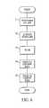
- FIG. 6depicts a flowchart describing an operational flow, in accordance with an exemplary embodiment of the invention.
- FIG. 7depicts a voltage arrangement across the PCRAM memory cell of FIG. 2;
- FIG. 8is a schematic diagram of a portion of the FIG. 3 circuit with added refresh circuitry.
- FIG. 9is a block diagram of a processor based system including a PCRAM memory device in accordance with the principles of the present invention.
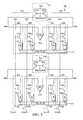
- FIG. 2illustrates a PCRAM cell 400 and in FIG. 3 a memory device 500 comprised of a plurality of PCRAM cells 400 a - 400 h.
- a PCRAM cell 400comprises an access transistor 401 , a programmable conductor memory element 402 , and a common cell plate 403 for a plurality of cells.
- the access transistor 401has its gate coupled to a word line 405 and one terminal coupled to a bit line 406 . A small portion of an array of such cells is shown in FIG.
- the bit lines 406 a, 406 a ′, and 406 b, 406 b ′are coupled to respective pre-charge circuits 501 a, 501 b, which can switchably supply a pre-charge potential to the bit lines 406 a, 406 a ′, 406 b, 406 b ′.
- each access transistor 401is coupled to one end of an associated programmable conductor memory element 402 , while the other end of the associated programmable conductor memory element 402 is coupled to the cell plate 403 .
- the cell plate 403may span and be coupled to several other PCRAM cells.
- the cell plate 403is also coupled to a potential source. In the exemplary embodiment the potential source is at (Vdd/2).
- the access transistor 401as well as the other access transistors, are depicted as N-type CMOS transistors, however, it should be understood that P-type CMOS transistors may be used as long as the corresponding polarities of the other components and voltages are modified accordingly.
- the programmable conductor memory element 402stores a binary “0” state when it has a resistance of approximately 10 K ohm, and a binary “1” when it has a resistance greater than 10 M ohm.
- the programmable conductor memory elementis normally at rest in a high resistive state but can be programmed to a low resistance state, e.g., binary “0” state, by applying a voltage greater than or equal to approximately +0.25 volt across the memory element.
- a memory element programmed to a low resistance statecan be programmed to a high resistance value, e.g., a binary “1” state, by applying a voltage greater than or equal to approximately ⁇ 0.25 volt across the memory element.
- the programmable conductorcan be nondestructively read by applying a reading voltage having a magnitude of less than 0.25 volt across the memory element. In the exemplary embodiment, the reading voltage of approximately 0.2 volt can be used. However, it should be readily apparent that other alternate voltages may be selected as required for programmable conductor memory elements formed of the indicated or other material compositions.
- FIG. 3illustrates a memory device 500 comprising a pair of memory arrays 550 a, 550 b.
- Each memory array 550 a, 550 bincludes a plurality of memory cells 400 a - 400 d, 400 e - 400 h arranged such that the memory cells 400 along any given bit line 406 a, 406 a ′, 406 b, 406 b ′ do not share a common word line 405 a - 405 d. Conversely, the memory cells 400 along any word line 405 a - 405 d do not share a common bit line 406 a, 406 a ′, 406 b, 406 b ′.
- a selected word lineis switchably coupled to an associated word line driver 512 a - 512 d via a transistor 510 a - 510 d in accordance with the output of a row decoder.
- a bit line 406 a, 406 a ′, 406 b, 406 b ′is selected for use in accordance with the output of a column decoder.
- Each memory array 550 a, 550 bhas its own set of bit lines. For example, memory array 550 a includes bit lines 406 a, 406 b, while memory array 550 b includes bit lines 406 a ′, 406 b ′.
- bit lines from each adjacent pair of memory arrays 550 a, 550 bare coupled to a common sense amplifier 300 a, 300 b.
- bit lines 406 a, 406 a ′are coupled to sense amplifier 300 a
- bit lines 406 b, 406 b ′are coupled to sense amplifier 300 b.
- FIG. 5illustrates a memory device having only two arrays 550 a, 550 b, and eight cells 400 a - 400 h. However, it should be understood that the illustrated memory device would typically have significantly more cells and arrays.
- the memory device 500also includes a plurality of pre-charge circuits 501 a - 501 b.
- One pre-charge circuite.g., 501 a
- One pre-charge circuitis shown as being provided for each pair of bit lines coupled to a sense amplifier (e.g., 406 a, 406 a ′), however, other pre-charge arrangements are also possible.
- Each pre-charge circuite.g., 501 a
- Each pre-charge circuitincludes two transistors (e.g., 502 a, 502 b ). One terminal of each transistor is coupled to a potential source Vdd. In the exemplary embodiment, the potential source Vdd is 2.5 volts.
- each transistore.g., 502 a, 502 b
- the gate of the each transistoris coupled to a pre-charge control signal.
- the transistorse.g., 502 a, 502 b
- the transistorsare P-MOS type transistor.
- the transistorsconduct, thereby pre-charging the bit lines (e.g., 406 a, 406 a ′).
- the transistorse.g., 502 a, 502 b
- the transistorsare switched off. Due to capacitance inherent in the bit lines (e.g., 406 a, 406 a ′), the bit lines will hold the pre-charge voltage level of 2.5 volts for a period of time.
- Reading a PCRAM cell, for example, cell 400 a, in the PCRAM device 500comprises the operations of accessing a memory element and sensing/refreshing the memory element.
- bit linese.g., 406 a, 406 a ′
- sense amplifiere.g. 300 a
- One of the bit lines, e.g. 406 amaintains an applied pre-charge voltage as a reference for the sense amplifier 300 a
- the other bit line e.g. 406 a ′starts with a voltage slightly higher than the pre-charge voltage due to parasitic capacitance between that bit line and an associated row line of the cell 400 being read, e.g. 400 a.
- bit line 406 athe voltage on bit line 406 a is discharged through memory element e.g. 402 a.
- This small potential difference between the reference voltage and the discharging voltage on bit line 406 acan be sensed by sense amplifier 300 a to determine the resistance and logical state of memory element 400 a.
- the read operationbegins with the pre-charging of the bit lines 406 a, 406 a ′, 406 b, 406 b ′ of the memory device 500 via pre-charge circuits 501 a - 501 b (step S 1 ).
- the bit linesmay be pre-charged by temporarily bringing the pre-charge signal low, causing transistors 502 a - 502 d to conduct the pre-charge voltage (Vdd) to the bit lines 406 a, 406 a ′, 406 b, 406 b ′.
- the transistors 502 a - 502 dstop conducting, but the bit lines 406 a, 406 a ′, 406 b, 406 b ′ will remain at the pre-charge potential for a predetermined period due to the capacitance inherent in the bit lines.
- the precharge periodis illustrated as the time prior to T 1 in FIGS. 4A, 4 B.
- a selected pair of bit lines e.g. 406 a, 406 a ′are pre-charged to 2.5 volts and the cell plate 403 a, 403 b is tied to 1.25 volts (Vdd/2).
- the pre-charge voltage in bit line 406 ais slightly higher as noted, e.g. to 2.6 volts when row line 405 a is activated.
- the row lineis activated at time T 1 (FIGS. 4A, 4 B), e.g. row line 405 a, there is a voltage drop across the access transistor, e.g. 401 a, which causes a voltage of approximately 0.2 volts to appear across the memory element 402 a.
- the potential difference between the bit line 406 a and the cell plate 403 awill cause the bit line to discharge to the cell plate through the conducting access transistor 401 and the programmable conductor memory element 402 a.
- the discharge rateis dependent upon the resistive state of the programmable conductor memory element 402 . That is, a low resistive state will cause the voltage on selected bit line 406 a to discharge faster than a high resistive state. As the bit line discharges, its voltage will fall from the original voltage of approximately 2.6 volts toward the cell plate voltage.
- the word lines 405 a - 405 dare normally at ground potential.
- the access transistors 401 a - 401 dare normally switched off.
- the word line 405 a associated with a cell 400 a to be readis activated by bringing its potential from ground to a predetermined level (step S 2 in FIG. 6 ).
- the predetermined levelis designed to create a reading voltage at the programmable element 402 a, which as previously explained, must have a magnitude less than the magnitude of a writing voltage.
- the word line 405 ais brought to approximately 2.25 volts.
- the potential at the interface between the transistor 401 a and the programmable element 402 ais 1.45 volt. This results in a reading voltage of 0.2 volt across the programmable memory element 402 a since the voltage at the interface between the programmable element 402 a and the cell plate 403 a is maintained at 1.25 volt.
- bit lines 406 aAs noted, due to the inherent parasitic capacitance between the word line 401 a and its associated bit lines 406 a the potential in the associated bit line 406 a increase as the word line 401 a is activated. In the exemplary embodiment, the potential in bit line 406 a increases by 0.1 volt to 2.6 volt. It should be noted that the word lines 405 c, 405 d coupled to complementary bit lines 406 a ′, 406 b ′ remain at ground potential. Thus, bit lines 406 a ′, 406 b ′ remain at the pre-charge potential, which is 2.5 volt in the exemplary embodiment.
- bit line 406 ais used in combination with the two bi-stable resistive states of the programmable element 402 a to cause one of the bit lines (e.g., 406 a ) coupled to a sense amplifier (e.g., 300 a ) to have either a greater or lesser voltage than the other bit line (e.g., 406 a ′) coupled to the same sense amplifier 300 a.
- the memoryis designed and operated so that if the programmable element 402 a has a high resistive state, bit line 406 a discharges more slowly, thereby causing it to maintain its relatively higher potential.
- bit line 406 adischarges at a faster rate, so that bit line 406 transitions to a lower potential state than bit line 406 a ′.
- FIG. 5is detailed illustration of a sense amplifier 300 , which comprises a N-sense amp 310 N and a P-sense amp portion 310 P.
- the N-sense amp 310 N and the P-sense amp 310 Pinclude nodes NLAT* and ACT, respectively. These nodes are coupled to controllable potential sources (not illustrated) which supply control signals which respectively turn on the N-sense amp 310 N and the P-sense amp 310 P.
- the transistors, 301 - 304 of the N- and P-sense amps 310 N, 310 Pare switched off and no enabling signals are supplied to the NLAT* and ACT modes.
- the sense operation of sense amplifier 300is a two phased operation in which the N-sense amp 310 N is triggered before the P-sense amp 310 P.
- the N-sense amp 310 Nis triggered by bringing the potential at node NLAT* towards ground potential.
- the potential difference between node NLAT* and the bit lines 106 A and 106 a ′approach the threshold potential of NMOS transistors 301 , 302 , the transistor with the gate coupled to the higher voltage bit line begins to conduct. This causes the lower voltage bit line to discharge towards the voltage of the NLAT* node.
- the lower voltage bit linewill also reach ground potential.
- the other NMOS transistornever conducts since its gate is coupled to the low voltage digit line being discharged towards ground.
- the P-sense amp 310 Pis triggered (after the N-sense amp 310 N has been triggered) by bringing the potential at node ACT from ground towards Vdd. As the potential of the lower voltage bit line approaches ground (caused by the earlier triggering of the N-sense amp 310 N), the PMOS transistor with its gate coupled to the lower potential bit line will begin to conduct. This causes the initially higher potential bit line to be charged to a potential Vdd. After both the N- and P-sense amps 310 N, 310 P have been triggered, the higher voltage bit line has its potential elevated to Vdd while the lower potential bit line has it potential reduced to ground.
- the process of triggering both sense amps 310 N, 310 Pamplifies the potential difference created by the access operation to a level suitable for use in digital circuits.
- the bit line 106 a associated with the memory cell 400 a being readis driven to ground if the memory cell 400 a stored a charge corresponding to a binary 0, or to Vdd if the memory cell 400 a stored a charge corresponding to a binary 1, thereby permitting a compactor (or differential amplifier) 350 a coupled to bit lines 106 a, 106 a ′ to output a binary 0 or 1 consistent with the data stored in the cell 400 a on signal line 351 .
- the N-sense amplifier 310 Nis activated (start of step S 3 ).
- activating the N-sense amplifiercauses the bit line (one of 406 a and 406 a ′) having the lower potential to be pulled with the NLAT signal toward ground.
- T 2is approximately 30 nanosecond after the world line activation at T 1 .
- the timing of T 2may be varied without departing from spirit or scope of the invention.
- T 3the P-sense amplifier 310 P is activated.
- activating the P-sense amplifiercauses the bit line (one of 406 a and 406 a ′) having the higher potential to be pulled towards Vdd.
- T 3is approximately 35 nanosecond after T 1 (end of step S 3 ).
- the timing of T 4may also be varied without departing from spirit or scope of the invention.
- one of the bit lines 406 a, 406 a ′is at ground and the other is at Vdd, depending on the resistance of cell 400 a. Since one bit line coupled to sense amplifier 300 a is now at ground potential while the other bit line is now at Vdd potential, a comparator (or differential amplifier) 350 can be used to output a value corresponding to the contents of the cell 400 a on signal line 351 a.
- FIG. 7shows a voltage chart describing a re-write/refresh operation for a read memory cell 400 a in accordance with an exemplary embodiment of the invention.
- the following parameters of the programmable conductor memory cellsare presumed: i) that the voltage across an element 402 required to write from a high resistance state to a low resistance state is 0.25V; and ii) that the voltage across elements 402 required to write from a low resistance state to a high resistance state is ⁇ 0.25V. It should be readily apparent that alternative voltages may be used depending on the material composition, size and construction of the programmable conductor memory element 402 .
- the write processbegins at step S 4 by first writing to the opposite data that was sensed at step S 3 .
- the cellis first written to the opposite or complement data (i.e., “0” state), as shown in step S 4 , and then written back to the correct read state (i.e., “1”), as shown in step S 5 .
- the cellis first written to the opposite data state (i.e., “1”) and then written back to the correct data state (i.e., “0”).
- a read memory elementcan be set to a particular logic state.
- a memory element 402 aonce a memory element 402 a is read, it is refreshed by first writing the logic state of the memory element to its complementary state and then writing it back again to its original logic state.
- a read memory element 402 aholds a high resistance state e.g. logic “1,” it is refreshed by first writing it to a low resistance state, e.g. logic “0.” And then writing it again to a high resistance state e.g. logic “1.”
- FIG. 8illustrates one exemplary refresh circuit which can be used to refresh a read memory element.
- FIG. 8illustrates a portion of the FIG. 3 memory structure including the memory cell 400 a including access transistor 401 a and memory element 402 a. Also shown is a bit line charge circuit 911 which is used following a read operation to set bit line 406 a to voltage of either Vdd or ground.
- FIG. 8also illustrates a refresh signal generating circuit 921 for generating the refresh signal applied to control the bit line charge circuit 911 .
- the refresh signal generating circuit 921includes an inverter 903 which receives an output signal from bit line 406 a and a delay circuit 905 .
- the timing diagram of FIG. 4Ashows the bit line 406 a as having a value of Vdd after a read operation at time T 4 . Because the voltage on bit line 406 a is Vdd and the word line 405 a has been turned to 2.5V, the high resistance state of memory element 402 a is read, and the Vdd on the bit line will cause the memory element to see +0.25 volts across it which will automatically program it to a low resistance state before time T 4 when a read operation is completed.
- bit line 406 ais brought to ground by an inversion of the Vdd value in inverter 903 and application of the inverted bit line 406 a voltage as an input to bit line charge circuit 911 and drop the bit line voltage to ground at time T 5 . Then, if word line 405 a is then enabled, as shown at time T 6 in FIG. 4A, there will be a negative 0.25 volt across the memory element 402 a which is sufficient to reprogram it back to a high resistance state.
- FIG. 4Ashows word line 405 a disabled at time T 4 and re-enabled at time T 6 , it is also possible to keep word line 405 a enabled through the time period T 4 to T 7 .
- FIG. 4Bif the memory element 402 a originally held a low resistance value, prior to time T 4 , the ground voltage on the bit line 406 a produced by the sense amplifier 300 a will produce a negative 0.25 volts across the memory element 402 a automatically programming it to a high resistance state.
- bit line 406 aThe ground voltage on the bit line 406 a is converted to a Vdd voltage by inverter 903 and the delayed inverted signal is applied to bit line charge circuit 911 to apply a voltage of Vdd to bit line 406 a at T 5 .
- word line 405 ais enabled at T 6 to program the memory element 402 a back to a low resistance state. Again, word line 405 a in FIG. 4B can also remain enabled during the period T 4 to T 7 if desired.
- An enable transistor 917 controlled by an applied enable signalcan be used to enable or disable operation of the bit line charge circuit 911 by a refresh operation.
- the inventionmay also be used to only write a complementary resistance value a back to a memory element after a read operation.
- Thiscan be implemented by eliminating the bit line charge circuit 911 and refresh signal generating circuit 921 in FIG. 8 and only performing the first write operation illustrated in FIGS. 4A, 4 B, that is, the refresh operation up to time T 4 .
- each time a read operation occursthe memory element is refreshed to its complementary logic state.
- a flip flop 951 or other logic element receiving a delayed output from the sense amplifier 300 ais used to control an output data inverter 953 to enable/disable the inverter to ensure a proper logic state is output from a memory element 402 a.
- the output of the sense amplifieris again delayed and used to toggle flip flop 951 back to a “0” state which will not enable inverter 953 on a subsequent read operation. Since the “0” read by sense amplifier 300 a will be rewritten in memory element 402 a as a “1,” the next time the memory element 402 a is read the stored “1” value will be read out and not inverted. This process repeats for each read of memory element 402 a.
- FIG. 9is a block diagram of a processor based system 800 , such as a computer system, containing a PCRAM semiconductor memory 802 as described in connection with the other figures.
- the memory 802may be constituted as one or more memory chips or memory integrated circuits mounted on a memory module, for example, a plug-in memory module such as a SIMM, DIMM, or other plug-in memory module.
- the processor based system 800includes a processor 801 , a memory 802 , a mass storage 803 , and an I/O device 804 , each coupled to a bus 805 . While a single processor 801 is illustrated, it should be understood that processor 801 could be any type of processor and may include multiple processor and/or processors and co-processors.
- Memory 802is illustrated in FIG. 9 as having a plurality of PCRAM devise 500 .
- memory 802may only include a single PCRAM device 500 , or a larger plurality of PCRAM devices 500 than illustrated, and/or may include additional forms of memories, such as non-volatile memory or cache memories.
- the processor based system 800may include a plurality of mass storage devices, possibly of varying types such as, but not limited to, floppy disks, CDROMs, CD-R, CD-RW, DVD, hard disks, and disk arrays.
- I/O device 804may likewise comprise a plurality of I/O devices of varying tepes, including, but not limited to keyboard, mouse, graphic cards, monitors, and network interfaces.
- Bus 805while illustrated as a single bus may comprise a plurality of buses and/or bridges, which may be coupled to each other or bridged by other components. Some of the devices 801 - 804 may be coupled to only a single bus 805 , others may be coupled to a plurality of buses 805 .
Landscapes
- Dram (AREA)
- Semiconductor Memories (AREA)
Abstract
Description
The present invention relates to integrated memory circuits. More specifically, it relates to a method for writing a programmable conductor random access memory (PCRAM) cell.
Dynamic random access memory (DRAM) integrated circuit arrays have existed for more than thirty years and their dramatic increase in storage capacity has been achieved through advances in semiconductor fabrication technology and circuit design technology. The tremendous advances in these two technologies have also achieved higher levels of integration that permit dramatic reductions in memory array size and cost, as well as increased process yield.
FIG. 1 is a schematic diagram of aDRAM memory cell 100 comprising anaccess transistor 101 and acapacitor 102. Thecapacitor 102, which is coupled to a Vcc/2 potential source and thetransistor 101, stores one bit of data in the form of a charge. Typically, a charge of one polarity (e.g., a charge corresponding to a potential difference across thecapacitor 102 of +Vcc/2) is stored in thecapacitor 102 to represent a binary “1” while a charge of the opposite polarity (e.g., a charge corresponding to a potential difference across thecapacitor 102 of −Vcc/2) represents a binary “0.” The gate of thetransistor 101 is coupled to aword line 103, thereby permitting theword line 103 to control whether thecapacitor 102 is conductively coupled via thetransistor 101 to abit line 104. The default state of eachword line 103 is at ground potential, which causes thetransistor 101 to be switched off, thereby electrically isolatingcapacitor 102.
One of the drawbacks associated withDRAM cells 100 is that the charge on thecapacitor 102 may naturally decay over time, even if thecapacitor 102 remains electrically isolated. Thus,DRAM cells 100 require periodic refreshing. Additionally, as discussed below, refreshing is also required after amemory cell 100 has been accessed, for example, as part of a read operation.
Efforts continue to identify other forms of memory elements for us in memory cells, particularly for memory elements which do not required frequent refresh operations. Recent studies have focused on resistive materials that can be programmed to exhibit either high or low stable ohmic states. A programmable resistance element of such material could be programmed (set) to a high resistive state to store, for example, a binary “1” data bit or programmed (set) to a low resistive state to store a binary “0,” data bit. The stored data bit could then be read by detecting the magnitude of a readout current switched through the resistive memory element by an access device, thus indicating its programmed stable resistance state.
Recently programmable conductor materials, such as chalcogenide glasses, have been investigated as data storage memory cells for use in memory devices. U.S. Pat. Nos. 5,761,115, 5,896,312, 5,914,893, and 6,084,796 all describe chalcogenide glass materials which can be used as programmable conductor memory elements and are incorporated herein by reference. One characteristic of such an element is that it typically includes a chalcogenide glass which is doped with metal ion and a cathode and anode spaced apart on a surface of the glass. Application of a voltage across the cathode and anode causes the glass to achieve a low resistance state. One theory for this is that the applied voltage causes growth of a nearly non-volatile metal dendrite in or on the surface of the glass which changes the resistance and capacitance of the memory element which can then be used to store data.
One particularly promising programmable conductor material is a chalcogenide glass formed as an alloy system including Ge:Se:Ag for example, a Gex:Se(1−x)composition which is doped with silver. A memory element comprised of a chalcogenide glass has a natural stable high resistive state but can be programmed to a low resistance state by passing a current pulse from a voltage of suitable polarity through the cell. A chalcogenide memory element is simply written over by the appropriate current pulse and voltage polarity (reverse of that which writes the cell to a low resistance state) to reprogram it, and thus does not need to be erased. Moreover, a memory element of chalcogenide material is nearly nonvolatile, in that it need only be rarely refreshed in order to retain its programmed low resistance state. Such memory cells, unlike DRAM cells, can be accessed without requiring a refresh.
Since there is a considerable body of known and proven circuitry for reading, writing and refreshing DRAM memory cells, it would be desirable to use the same or similar circuitry with programmable conductor memory elements. However, while conventional read sense amplifier circuitry, associated with DRAM cells, are capable of use in accessing and sensing programmable element random access memory (PCRAM) cells, the natural refresh operation associated with these sense amplifiers is not required for a programmable conductor memory element. Indeed, frequent rewriting of PCRAM memory elements to the same state is not desirable because it can cause the memory element to wear out faster. Accordingly, there is a need and desire for a circuit and method for writing PCRAM cells without causing premature deterioration.
The present invention provides an improved method for reading a programmable conductor memory element which reduces premature deterioration due to repeated refresh operations. This is accomplished by first performing a read operation on a memory element and then writing the memory element to the opposite or complement logical state from the state which was read and then writing the memory element back to the original logical state. Hence, if following a high resistance state read operation the memory element is to be written to a high resistance state, then the memory element is first written to the opposite state (i.e., low resistance state) and then written back to the original state (i.e., high resistance state). Alternatively, if following a low resistance state read operation the PCRAM cells are to be written to a low resistance state, then the cells are first written to the opposite state (i.e., high resistance state) and then written back to the original state (i.e., low resistance state).
In an alternative embodiment, after a read operation the memory element may simply be re-written to a state complementary to the read state and logic circuitry associated with a memory device containing the memory element keeps track during a read operation if the read data should output as read or after being inverted. For example, if a high resistance state represents a “1” data value and a low resistance state represents a “0” data value, and if a memory element is read as a “1” that memory element will be written to a “0” state following the read operation. During a subsequent read of the same memory element, as a “0” the logic circuitry will invert the logic state and output it correctly as a “1.” After the subsequent read, the memory element will then be written to a “1” state and the logic circuit will note that no logical state inversion is required for the next read of the memory element.
The foregoing and other advantages and features of the invention will become more apparent from the detailed description of exemplary embodiments of the invention given below with reference to the accompanying drawings in which:
FIG. 1 is a schematic diagram of a conventional DRAM cell;
FIG. 2 is a schematic diagram of a PCRAM cell;
FIG. 3 is a schematic diagram a PCRAM array;
FIGS. 4A and 4B are timing diagrams illustrating the voltages on the word and bit lines when a PCRAM cell is read in high resistance and low resistance states, respectively;
FIG. 5 is a schematic diagram of a sense amplifier used in the invention;
FIG. 6 depicts a flowchart describing an operational flow, in accordance with an exemplary embodiment of the invention;
FIG. 7 depicts a voltage arrangement across the PCRAM memory cell of FIG. 2;
FIG. 8 is a schematic diagram of a portion of the FIG. 3 circuit with added refresh circuitry; and
FIG. 9 is a block diagram of a processor based system including a PCRAM memory device in accordance with the principles of the present invention.
Referring to the drawings, where like reference numerals designate like elements, FIG. 2 illustrates aPCRAM cell 400 and in FIG. 3 amemory device 500 comprised of a plurality ofPCRAM cells 400a-400h.As illustrated in FIG. 2, aPCRAM cell 400 comprises anaccess transistor 401, a programmableconductor memory element 402, and acommon cell plate 403 for a plurality of cells. Theaccess transistor 401 has its gate coupled to aword line 405 and one terminal coupled to abit line 406. A small portion of an array of such cells is shown in FIG. 3 as includingbit lines word lines bit lines pre-charge circuits bit lines access transistor 401 is coupled to one end of an associated programmableconductor memory element 402, while the other end of the associated programmableconductor memory element 402 is coupled to thecell plate 403. Thecell plate 403 may span and be coupled to several other PCRAM cells. Thecell plate 403 is also coupled to a potential source. In the exemplary embodiment the potential source is at (Vdd/2).
Theaccess transistor 401, as well as the other access transistors, are depicted as N-type CMOS transistors, however, it should be understood that P-type CMOS transistors may be used as long as the corresponding polarities of the other components and voltages are modified accordingly. The programmableconductor memory element 402 is preferably made of chalcogenide glass having a Gex:Se:(1−x)composition (e.g., x=0.2 to 0.3) which is doped with silver, however, it should be understood that any other bi-stable programmable conductor material known to those with ordinary skill in the art may also be used. In the exemplary embodiment of a Gex:Se:(1−x)glass where x=0.2 to 0.3, the programmableconductor memory element 402 stores a binary “0” state when it has a resistance of approximately 10 K ohm, and a binary “1” when it has a resistance greater than 10 M ohm. The programmable conductor memory element is normally at rest in a high resistive state but can be programmed to a low resistance state, e.g., binary “0” state, by applying a voltage greater than or equal to approximately +0.25 volt across the memory element. A memory element programmed to a low resistance state can be programmed to a high resistance value, e.g., a binary “1” state, by applying a voltage greater than or equal to approximately −0.25 volt across the memory element. The programmable conductor can be nondestructively read by applying a reading voltage having a magnitude of less than 0.25 volt across the memory element. In the exemplary embodiment, the reading voltage of approximately 0.2 volt can be used. However, it should be readily apparent that other alternate voltages may be selected as required for programmable conductor memory elements formed of the indicated or other material compositions.
FIG. 3 illustrates amemory device 500 comprising a pair ofmemory arrays memory array memory cells 400a-400d,400e-400harranged such that thememory cells 400 along any givenbit line common word line 405a-405d.Conversely, thememory cells 400 along anyword line 405a-405ddo not share acommon bit line bit line memory array memory array 550aincludesbit lines memory array 550bincludesbit lines 406a′,406b′. The bit lines from each adjacent pair ofmemory arrays common sense amplifier bit lines sense amplifier 300a,whilebit lines sense amplifier 300b.For simplicity, FIG. 5 illustrates a memory device having only twoarrays cells 400a-400h.However, it should be understood that the illustrated memory device would typically have significantly more cells and arrays.
Thememory device 500 also includes a plurality of pre-charge circuits501a-501b.One pre-charge circuit (e.g.,501a) is shown as being provided for each pair of bit lines coupled to a sense amplifier (e.g.,406a,406a′), however, other pre-charge arrangements are also possible. Each pre-charge circuit (e.g.,501a) includes two transistors (e.g.,502a,502b). One terminal of each transistor is coupled to a potential source Vdd. In the exemplary embodiment, the potential source Vdd is 2.5 volts. Another terminal of each transistor (e.g.,502a,502b) is coupled to its corresponding bit line (e.g.,406a,406a′, respectively). The gate of the each transistor (e.g.,502a,502b) is coupled to a pre-charge control signal. As illustrated, the transistors (e.g.,502a,502b) are P-MOS type transistor. Thus, when the pre-charge signal is low, the transistors (e.g.,502a,502b) conduct, thereby pre-charging the bit lines (e.g.,406a,406a′). When the pre-charge signal is high, the transistors (e.g.,502a,502b) are switched off. Due to capacitance inherent in the bit lines (e.g.,406a,406a′), the bit lines will hold the pre-charge voltage level of 2.5 volts for a period of time.
Reading a PCRAM cell, for example,cell 400a,in thePCRAM device 500 comprises the operations of accessing a memory element and sensing/refreshing the memory element.
During a read operation a small potential difference is created between the bit lines (e.g.,406a,406a′) coupled to the same sense amplifier (e.g.,300a) for a memory cell e.g., a400a,being read. One of the bit lines, e.g.406amaintains an applied pre-charge voltage as a reference for thesense amplifier 300a,while the other bit line e.g.406a′ starts with a voltage slightly higher than the pre-charge voltage due to parasitic capacitance between that bit line and an associated row line of thecell 400 being read, e.g.400a.During a read operation fore.g. cell 400a,the voltage onbit line 406ais discharged through memory element e.g.402a.This small potential difference between the reference voltage and the discharging voltage onbit line 406acan be sensed bysense amplifier 300ato determine the resistance and logical state ofmemory element 400a.
Now also referring to FIG. 6, the read operation begins with the pre-charging of thebit lines memory device 500 via pre-charge circuits501a-501b(step S1). The bit lines may be pre-charged by temporarily bringing the pre-charge signal low, causing transistors502a-502dto conduct the pre-charge voltage (Vdd) to thebit lines bit lines
In the exemplary embodiment, a selected pair of bit lines e.g.406a,406a′, are pre-charged to 2.5 volts and thecell plate bit line 406ais slightly higher as noted, e.g. to 2.6 volts whenrow line 405ais activated. When the row line is activated at time T1 (FIGS. 4A,4B),e.g. row line 405a,there is a voltage drop across the access transistor, e.g.401a,which causes a voltage of approximately 0.2 volts to appear across thememory element 402a.The potential difference between thebit line 406aand thecell plate 403awill cause the bit line to discharge to the cell plate through the conductingaccess transistor 401 and the programmableconductor memory element 402a.The discharge rate is dependent upon the resistive state of the programmableconductor memory element 402. That is, a low resistive state will cause the voltage on selectedbit line 406ato discharge faster than a high resistive state. As the bit line discharges, its voltage will fall from the original voltage of approximately 2.6 volts toward the cell plate voltage.
In thememory device 500, theword lines 405a-405dare normally at ground potential. Thus theaccess transistors 401a-401dare normally switched off. Referring now to FIGS. 4A and 4B, at time T1, theword line 405aassociated with acell 400ato be read is activated by bringing its potential from ground to a predetermined level (step S2 in FIG.6). The predetermined level is designed to create a reading voltage at theprogrammable element 402a,which as previously explained, must have a magnitude less than the magnitude of a writing voltage. In the exemplary embodiment, theword line 405ais brought to approximately 2.25 volts. Since the voltage drop across thetransistor 401ais approximately 1.15 volts, the potential at the interface between thetransistor 401aand theprogrammable element 402ais 1.45 volt. This results in a reading voltage of 0.2 volt across theprogrammable memory element 402asince the voltage at the interface between theprogrammable element 402aand thecell plate 403ais maintained at 1.25 volt.
As noted, due to the inherent parasitic capacitance between theword line 401aand its associatedbit lines 406athe potential in the associatedbit line 406aincrease as theword line 401ais activated. In the exemplary embodiment, the potential inbit line 406aincreases by 0.1 volt to 2.6 volt. It should be noted that the word lines405c,405dcoupled tocomplementary bit lines 406a′,406b′ remain at ground potential. Thus,bit lines 406a′,406b′ remain at the pre-charge potential, which is 2.5 volt in the exemplary embodiment.
The increased potential ofbit line 406ais used in combination with the two bi-stable resistive states of theprogrammable element 402ato cause one of the bit lines (e.g.,406a) coupled to a sense amplifier (e.g.,300a) to have either a greater or lesser voltage than the other bit line (e.g.,406a′) coupled to thesame sense amplifier 300a.The memory is designed and operated so that if theprogrammable element 402ahas a high resistive state,bit line 406adischarges more slowly, thereby causing it to maintain its relatively higher potential. However, if theprogrammable element 402ahas a low resistive state,bit line 406adischarges at a faster rate, so thatbit line 406 transitions to a lower potential state thanbit line 406a′. These two effects can be seen by comparing FIG. 4A (illustrating the effects of a programmable element at a high resistive state) and FIG. 4B (illustrating the effects of a programmable element at a low resistive state.)
FIG. 5 is detailed illustration of a sense amplifier300, which comprises a N-sense amp 310N and a P-sense amp portion 310P. The N-sense amp 310N and the P-sense amp 310P include nodes NLAT* and ACT, respectively. These nodes are coupled to controllable potential sources (not illustrated) which supply control signals which respectively turn on the N-sense amp 310N and the P-sense amp 310P. In an initial state, the transistors,301-304 of the N- and P-sense amps sense amp 310N is triggered before the P-sense amp 310P.
The N-sense amp 310N is triggered by bringing the potential at node NLAT* towards ground potential. As the potential difference between node NLAT* and thebit lines 106A and106a′ approach the threshold potential ofNMOS transistors
The P-sense amp 310P is triggered (after the N-sense amp 310N has been triggered) by bringing the potential at node ACT from ground towards Vdd. As the potential of the lower voltage bit line approaches ground (caused by the earlier triggering of the N-sense amp 310N), the PMOS transistor with its gate coupled to the lower potential bit line will begin to conduct. This causes the initially higher potential bit line to be charged to a potential Vdd. After both the N- and P-sense amps amps bit line 106aassociated with thememory cell 400abeing read is driven to ground if thememory cell 400astored a charge corresponding to a binary 0, or to Vdd if thememory cell 400astored a charge corresponding to a binary 1, thereby permitting a compactor (or differential amplifier)350acoupled tobit lines cell 400aonsignal line 351.
Returning to FIGS. 4A and 4B, at time period T2, the N-sense amplifier 310N is activated (start of step S3). As previously noted, activating the N-sense amplifier causes the bit line (one of406aand406a′) having the lower potential to be pulled with the NLAT signal toward ground. In the exemplary embodiment, T2 is approximately 30 nanosecond after the world line activation at T1. However, it should be noted that the timing of T2 may be varied without departing from spirit or scope of the invention.
At time period T3, the P-sense amplifier 310P is activated. As previously noted, activating the P-sense amplifier causes the bit line (one of406aand406a′) having the higher potential to be pulled towards Vdd. In the exemplary embodiment, T3 is approximately 35 nanosecond after T1 (end of step S3). However, it should be noted that the timing of T4 may also be varied without departing from spirit or scope of the invention.
As shown in both FIGS. 4A and 4B at time T4 after both the N- and P-sense amplifies have been fired, one of thebit lines cell 400a.Since one bit line coupled tosense amplifier 300ais now at ground potential while the other bit line is now at Vdd potential, a comparator (or differential amplifier)350 can be used to output a value corresponding to the contents of thecell 400aonsignal line 351a.
Next, FIG. 7 shows a voltage chart describing a re-write/refresh operation for a readmemory cell 400ain accordance with an exemplary embodiment of the invention. In this exemplary process flow, the following parameters of the programmable conductor memory cells are presumed: i) that the voltage across anelement 402 required to write from a high resistance state to a low resistance state is 0.25V; and ii) that the voltage acrosselements 402 required to write from a low resistance state to a high resistance state is −0.25V. It should be readily apparent that alternative voltages may be used depending on the material composition, size and construction of the programmableconductor memory element 402.
Referring back to FIG. 6 after the read operation occurs, the write process begins at step S4 by first writing to the opposite data that was sensed at step S3. Hence, ifmemory cell 400ais to be written back to a “1,” state (from step S3) then the cell is first written to the opposite or complement data (i.e., “0” state), as shown in step S4, and then written back to the correct read state (i.e., “1”), as shown in step S5. Alternatively, ifmemory cell 400ais to be written back to a “0” state, then the cell is first written to the opposite data state (i.e., “1”) and then written back to the correct data state (i.e., “0”).
As shown in FIG. 7, and assuming Vdd=2.5 volts and Vdd/2=1.25 volts, to write aprogrammable memory element 402ato a low resistance state requires a voltage of greater than or equal to +0.25 across thememory element 402a.Thus, if the bit line voltage V1 is set to Vdd and theaccess transistor 401ais turned on to 2.5 volts, and if there is approximately a V2=1 volt drop or less across the transistor, the voltage V3 drop across the cell is +0.25 or higher which is sufficient to program it to a low resistance state.
Ifmemory element 402ais to be written to a high resistance state, then the voltage across thememory element 402amust be less than −0.25 volts. To obtain this the bit line voltage V1 can be set to ground and the word line is activated. If the voltage drop V2 across the transistor is again 1 volt or less, then the voltage drop across the memory element V2=−0.25, or less which is sufficient to program a memory element to a high resistance state.
Thus, by controlling the voltage on the bit line and word line following the memory element read operation, a read memory element can be set to a particular logic state. In the invention, once amemory element 402ais read, it is refreshed by first writing the logic state of the memory element to its complementary state and then writing it back again to its original logic state. Thus, if aread memory element 402aholds a high resistance state e.g. logic “1,” it is refreshed by first writing it to a low resistance state, e.g. logic “0.” And then writing it again to a high resistance state e.g. logic “1.”
FIG. 8 illustrates one exemplary refresh circuit which can be used to refresh a read memory element. FIG. 8 illustrates a portion of the FIG. 3 memory structure including thememory cell 400aincludingaccess transistor 401aandmemory element 402a.Also shown is a bitline charge circuit 911 which is used following a read operation to setbit line 406ato voltage of either Vdd or ground.
FIG. 8 also illustrates a refreshsignal generating circuit 921 for generating the refresh signal applied to control the bitline charge circuit 911. The refreshsignal generating circuit 921 includes aninverter 903 which receives an output signal frombit line 406aand adelay circuit 905.
The operation of the refresh circuit illustrated in FIG. 8 will now be explained with reference to the timing diagram shown in FIGS. 4A and 4B. The timing diagram of FIG. 4A shows thebit line 406aas having a value of Vdd after a read operation at time T4. Because the voltage onbit line 406ais Vdd and theword line 405ahas been turned to 2.5V, the high resistance state ofmemory element 402ais read, and the Vdd on the bit line will cause the memory element to see +0.25 volts across it which will automatically program it to a low resistance state before time T4 when a read operation is completed. In order to reprogram the memory element back to a high resistance state, thebit line 406ais brought to ground by an inversion of the Vdd value ininverter 903 and application of theinverted bit line 406avoltage as an input to bitline charge circuit 911 and drop the bit line voltage to ground at time T5. Then, ifword line 405ais then enabled, as shown at time T6 in FIG. 4A, there will be a negative 0.25 volt across thememory element 402awhich is sufficient to reprogram it back to a high resistance state. Although FIG. 4A showsword line 405adisabled at time T4 and re-enabled at time T6, it is also possible to keepword line 405aenabled through the time period T4 to T7. Likewise, as shown in FIG. 4B if thememory element 402aoriginally held a low resistance value, prior to time T4, the ground voltage on thebit line 406aproduced by thesense amplifier 300awill produce a negative 0.25 volts across thememory element 402aautomatically programming it to a high resistance state. The ground voltage on thebit line 406ais converted to a Vdd voltage byinverter 903 and the delayed inverted signal is applied to bitline charge circuit 911 to apply a voltage of Vdd to bitline 406aat T5. Thenword line 405ais enabled at T6 to program thememory element 402aback to a low resistance state. Again,word line 405ain FIG. 4B can also remain enabled during the period T4 to T7 if desired.
An enabletransistor 917 controlled by an applied enable signal can be used to enable or disable operation of the bitline charge circuit 911 by a refresh operation.
The invention may also be used to only write a complementary resistance value a back to a memory element after a read operation. This can be implemented by eliminating the bitline charge circuit 911 and refreshsignal generating circuit 921 in FIG.8 and only performing the first write operation illustrated in FIGS. 4A,4B, that is, the refresh operation up to time T4. In this embodiment, each time a read operation occurs, the memory element is refreshed to its complementary logic state. With this embodiment aflip flop 951 or other logic element receiving a delayed output from thesense amplifier 300a,is used to control anoutput data inverter 953 to enable/disable the inverter to ensure a proper logic state is output from amemory element 402a.For example, if the original logic value stored inmemory element 402ais a “1,” when this value is read out the first time thememory element 402awill be refreshed with a logic “0” value. The “1” data output from sense amplifier will be sensed, after a delay bydelay element 953, and flipflop 951 will be toggled from a “0” to a “1” value. The nexttime memory element 402ais read, the stored logic value of “0” needs to be output as a “1” andflip flop 951 which now holds a “1” value enablesinverter 953 so that the read “0” value frommemory element 402 is correctly output as a logic “1” value. The output of the sense amplifier is again delayed and used to toggleflip flop 951 back to a “0” state which will not enableinverter 953 on a subsequent read operation. Since the “0” read bysense amplifier 300awill be rewritten inmemory element 402aas a “1,” the next time thememory element 402ais read the stored “1” value will be read out and not inverted. This process repeats for each read ofmemory element 402a.
FIG. 9 is a block diagram of a processor basedsystem 800, such as a computer system, containing aPCRAM semiconductor memory 802 as described in connection with the other figures. Thememory 802 may be constituted as one or more memory chips or memory integrated circuits mounted on a memory module, for example, a plug-in memory module such as a SIMM, DIMM, or other plug-in memory module. The processor basedsystem 800 includes aprocessor 801, amemory 802, amass storage 803, and an I/O device 804, each coupled to abus 805. While asingle processor 801 is illustrated, it should be understood thatprocessor 801 could be any type of processor and may include multiple processor and/or processors and co-processors.Memory 802 is illustrated in FIG. 9 as having a plurality of PCRAM devise500. However,memory 802 may only include asingle PCRAM device 500, or a larger plurality ofPCRAM devices 500 than illustrated, and/or may include additional forms of memories, such as non-volatile memory or cache memories. While onemass storage 803 device is illustrated, the processor basedsystem 800 may include a plurality of mass storage devices, possibly of varying types such as, but not limited to, floppy disks, CDROMs, CD-R, CD-RW, DVD, hard disks, and disk arrays. I/O device 804 may likewise comprise a plurality of I/O devices of varying tepes, including, but not limited to keyboard, mouse, graphic cards, monitors, and network interfaces.Bus 805, while illustrated as a single bus may comprise a plurality of buses and/or bridges, which may be coupled to each other or bridged by other components. Some of the devices801-804 may be coupled to only asingle bus 805, others may be coupled to a plurality ofbuses 805.
While the invention has been described in detail in connection with the exemplary embodiment, it should be understood that the invention is not limited to the above disclosed embodiment. Rather, the invention can be modified to incorporate any number of variations, alternations, substitutions, or equivalent arrangements not heretofore described, but which are commensurate with the spirit and scope of the invention. For example, many different types of equivalent circuits can be used to supply the appropriate read and write voltages to the memory cells, e.g.400a.Accordingly, the invention is not limited by the foregoing description or drawings of specific exemplary embodiments, but is only limited by the scope of the appended claims.
Claims (42)
1. A memory device comprising,
a programmable conductor memory element;
an access circuit for coupling said memory element between an activated word line and an activated bit line during a read operation;
a sense amplifier coupled to said activated bit line for sensing a first logical state of said memory element; and
writing circuitry for writing said memory element first to a complement logical state of said first logic state in response to said read operation and then writing said memory element back to said first logical state.
2. The memory device ofclaim 1 , wherein said first logical state is a first higher resistance state and the complement logical state is a second lower resistance state.
3. The memory device ofclaim 1 , wherein said first logical state is a first lower resistance state and the complement logical state is a second higher resistance state.
4. The memory device ofclaim 1 , further comprising a pre-charge circuit for pre-charging the activated bit line and a reference bit line prior to a sensing operation of said sense amplifier, wherein said activated bit line and said reference bit line are coupled to the sense amplifier.
5. The memory device ofclaim 1 , wherein said writing circuitry further comprises a bit line charge circuit for setting a voltage for said bit line.
6. The memory device ofclaim 5 , wherein said writing circuitry further comprises a refresh signal generating circuit for generating a refresh signal applied to control said bit line charge circuit.
7. The memory device ofclaim 1 , wherein said access circuit comprises a transistor.
8. The memory device ofclaim 1 , wherein said programmable conductor memory element comprises a chalcogenide glass.
9. The memory device ofclaim 8 , wherein said chalcogenide glass comprises a Ge:Se: glass composition which is doped with silver.
10. A programmable conductor memory circuit comprising:
a programmable conductor memory element;
an access device for enabling a read and write access to said memory element; and
a circuit for operating said access device to read a logical value stored in said memory element and then, in response to reading said stored logical value, to write a complementary logic value into said memory element.
11. The memory circuit ofclaim 10 , further comprising:
a bit line and a sense amplifier coupled to said bit line and to a reference voltage line during at least a read access of said memory element, said sense amplifier sensing a logic state of said memory element and setting said bit line at a predetermined voltage depending on a sensed logic state of said memory element; and
said circuit enabling said access device to couple said memory element between a voltage source and said bit line for a read operation and for enabling said access device to couple said memory element between said voltage source and said bit line after said sense amplifier sets said bit line at said predetermined voltage.
12. The memory ofclaim 10 , further comprising a logic circuitry for keeping track during a read operation whether the read logical value should be output as read or inverted before being output.
13. The memory ofclaim 12 , wherein said logic circuitry further comprises a flip flop to control an output data inverter to output a proper logic value.
14. The memory device ofclaim 11 , further comprising a pre-charge circuit for pre-charging said bit line and said reference voltage line prior to a sensing operation of said sense amplifier.
15. The memory device ofclaim 10 , wherein said access device comprises a transistor.
16. The memory device ofclaim 10 , wherein said programmable conductor memory element comprises a chalcogenide glass.
17. The memory device ofclaim 16 , wherein said chalcogenide glass comprises a Ge:Se: glass composition which is doped with silver.
18. A processor based system comprising,
a processor; and
a memory coupled to said processor, said memory comprising:
a programmable conductor memory element;
an access circuit for coupling said memory element between an activated word line and an activated bit line during a read operation;
a sense amplifier coupled to said activated bit line for sensing a first logical state of said memory element; and
writing circuitry for writing said memory element first to a complement logical state of said first logic state in response to said read operation and then writing said memory element back to said first logical state.
19. The system ofclaim 18 , wherein said first logical state is a first higher resistance state and the complement logical state is a second lower resistance state.
20. The system ofclaim 18 , wherein said first logical state is a first lower resistance state and the complement logical state is a second higher resistance state.
21. The system ofclaim 18 , further comprising a pre-charge circuit for pre-charging the activated bit line and a reference bit line prior to a sensing operation of said sense amplifier, wherein said activated bit line and said reference bit line are coupled to the sense amplifier.
22. The system ofclaim 18 , wherein said writing circuitry further comprises a bit line charge circuit for setting a voltage for said bit line.
23. The system ofclaim 22 , wherein said writing circuitry further comprises a refresh signal generating circuit for generating a refresh signal applied to control said bit line charge circuit.
24. The system ofclaim 18 , wherein said access circuit comprises a transistor.
25. The system ofclaim 18 , wherein said programmable conductor memory element comprises a chalcogenide glass.
26. The system ofclaim 25 , wherein said chalcogenide glass comprises a Ge:Se: glass composition which is doped with silver.
27. A processor based system comprising,
a processor; and
a memory coupled to said processor, said memory comprising:
a programmable conductor memory element;
an access device for enabling a read and write access to said memory element; and
a circuit for operating said access element to read a logical value stored in said memory device and then, in response to reading said stored logical value, to write a complementary logic value into said memory element.
28. The system ofclaim 27 , further comprising:
a bit line and a sense amplifier coupled to said bit line and to a reference voltage line during at least a read access of said memory element, said sense amplifier sensing a logic state of said memory element and setting said bit line at a predetermined voltage depending on a sensed logic state of said memory element; and
said circuit enabling said access device to couple said memory element between a voltage source and said bit line for a read operation and for enabling said access device to couple said memory element between said voltage source and said bit line after said sense amplifier sets said bit line at said predetermined voltage.
29. The system ofclaim 27 , further comprising a logic circuitry for keeping track during said read operation whether the read logical value should be output as read or inverted before being output.
30. The system ofclaim 29 , wherein said logic circuitry further comprises a flip flop to control an output data inverter to output a proper logic value.
31. The system ofclaim 27 , further comprising a pre-charge circuit for pre-charging said bit line and said reference voltage line prior to a sensing operation of said sense amplifier.
32. The system ofclaim 27 , wherein said access device comprises a transistor.
33. The system ofclaim 27 , wherein said programmable conductor memory element comprises a chalcogenide glass.
34. The system ofclaim 33 , wherein said chalcogenide glass comprises a Ge:Se: glass composition which is doped with silver.
35. A method for operating a programmable conductor random access memory element, said method comprising:
sensing a logical value stored in said memory element;
writing a logical value which is the complement of the read logical value to said memory element in response to said act of sensing.
36. The method ofclaim 35 , further comprising the act of writing said sensed logical value after writing said complement logical value.
37. The method ofclaim 35 , wherein said read logical value is stated in said memory element as a resistance value.
38. The method ofclaim 35 , wherein said programmable conductor memory cell comprises a chalcogenide glass.
39. The method ofclaim 38 , wherein said chalcogenide glass comprises a Ge:Se: glass composition which is doped with silver.
40. A method for writing data to a programmable conductor random access memory element, said method comprising:
pre-charging a first bit line coupled to the programmable conductor random access memory element to a first voltage value;
pre-charging a second bit line to a second voltage value, said first value being different from said second value;
enabling an access transistor to couple the programmable conductor memory element to said first bit line;
sensing voltage on said first bit line and said second bit line to determine a first logical state of said programmable conductor memory element; and
writing a second logical state complementary to said first logical state to said memory element after said first logical state is determined.
41. The method ofclaim 40 , wherein said programmable conductor memory element comprises a chalcogenide glass.
42. The method ofclaim 41 , wherein said chalcogenide glass comprises a Ge:Se: glass composition which is doped with silver.
Priority Applications (1)
| Application Number | Priority Date | Filing Date | Title |
|---|---|---|---|
| US10/137,554US6731528B2 (en) | 2002-05-03 | 2002-05-03 | Dual write cycle programmable conductor memory system and method of operation |
Applications Claiming Priority (1)
| Application Number | Priority Date | Filing Date | Title |
|---|---|---|---|
| US10/137,554US6731528B2 (en) | 2002-05-03 | 2002-05-03 | Dual write cycle programmable conductor memory system and method of operation |
Publications (2)
| Publication Number | Publication Date |
|---|---|
| US20030206433A1 US20030206433A1 (en) | 2003-11-06 |
| US6731528B2true US6731528B2 (en) | 2004-05-04 |
Family
ID=29269102
Family Applications (1)
| Application Number | Title | Priority Date | Filing Date |
|---|---|---|---|
| US10/137,554Expired - LifetimeUS6731528B2 (en) | 2002-05-03 | 2002-05-03 | Dual write cycle programmable conductor memory system and method of operation |
Country Status (1)
| Country | Link |
|---|---|
| US (1) | US6731528B2 (en) |
Cited By (46)
| Publication number | Priority date | Publication date | Assignee | Title |
|---|---|---|---|---|
| US20040032782A1 (en)* | 2001-10-24 | 2004-02-19 | Glen Hush | System and method for power saving memory refresh for dynamic random access memory devices after an extended interval |
| US20040160817A1 (en)* | 2002-08-02 | 2004-08-19 | Unity Semiconductor Corporation | Non-volatile memory with a single transistor and resistive memory element |
| US20040240306A1 (en)* | 2002-04-18 | 2004-12-02 | Pierre Fazan | Data storage device and refreshing method for use with such device |
| US20050098811A1 (en)* | 2003-11-12 | 2005-05-12 | Ryu Ogiwara | Phase-change memory device using chalcogenide compound as the material of memory cells |
| US20060044878A1 (en)* | 2004-09-02 | 2006-03-02 | Perner Frederick A | Programming of programmable resistive memory devices |
| US20060044906A1 (en)* | 2004-09-01 | 2006-03-02 | Ethan Williford | Sensing of resistance variable memory devices |
| US20060083055A1 (en)* | 2002-08-02 | 2006-04-20 | Unity Semiconductor Corporation | Providing a reference voltage to a cross point memory array |
| US20060094236A1 (en)* | 2004-11-03 | 2006-05-04 | Elkins Patricia C | Electroless plating of metal caps for chalcogenide-based memory devices |
| US20060097775A1 (en)* | 2004-11-11 | 2006-05-11 | International Business Machines Corporation | Circuit and Method of Controlling Integrated Circuit Power Consumption Using Phase Change Switches |
| US20060097344A1 (en)* | 2001-09-21 | 2006-05-11 | Casper Michael D | Integrated thin film capacitor/inductor/interconnect system and method |
| US20060104142A1 (en)* | 2002-08-29 | 2006-05-18 | Gilton Terry L | Software refreshed memory device and method |
| US20060164882A1 (en)* | 2004-12-23 | 2006-07-27 | Robert Norman | Storage controller using vertical memory |
| US20060168505A1 (en)* | 2005-01-26 | 2006-07-27 | Corvin Liaw | Integrated memory device and method for operating the same |
| US20060166430A1 (en)* | 2003-11-10 | 2006-07-27 | Darrell Rinerson | Conductive memory stack with non-uniform width |
| US20060171200A1 (en)* | 2004-02-06 | 2006-08-03 | Unity Semiconductor Corporation | Memory using mixed valence conductive oxides |
| US20060245241A1 (en)* | 2004-07-20 | 2006-11-02 | Darrell Rinerson | Two terminal memory array having reference cells |
| US20060243956A1 (en)* | 2002-08-02 | 2006-11-02 | Unity Semiconductor Corporation | Cross point memory array with fast access time |
| US20060245243A1 (en)* | 2004-02-06 | 2006-11-02 | Darrell Rinerson | Multi-resistive state element with reactive metal |
| US20070025144A1 (en)* | 2005-07-29 | 2007-02-01 | International Business Machines Corporation | Write operations for phase-change-material memory |
| US20070041251A1 (en)* | 2005-08-16 | 2007-02-22 | Thomas Roehr | Electrical circuit and a method for operating a programmable metallization cell |
| US20070047291A1 (en)* | 2005-08-26 | 2007-03-01 | Heinz Hoenigschmid | Integrated memory circuit comprising a resistive memory element and a method for manufacturing such a memory circuit |
| US20070058417A1 (en)* | 2005-09-08 | 2007-03-15 | Thomas Roehr | Method for writing data into a memory cell of a conductive bridging random access memory, memory circuit and CBRAM memory circuit |
| US20070070690A1 (en)* | 2005-09-28 | 2007-03-29 | Scheuerlein Roy E | Method for using a multi-use memory cell and memory array |
| US20070171697A1 (en)* | 2005-12-23 | 2007-07-26 | Heinz Hoenigschmid | CBRAM memory device and method for writing to a resistive memory cell in a CBRAM memory device |
| US20070195580A1 (en)* | 2006-02-23 | 2007-08-23 | Heinz Hoenigschmid | Memory circuit having a resistive memory cell and method for operating such a memory circuit |
| US20070211514A1 (en)* | 2006-03-13 | 2007-09-13 | Corvin Liaw | Memory circuit, method for operating a memory circuit, memory device and method for producing a memory device |
| US20070211515A1 (en)* | 2004-08-30 | 2007-09-13 | Infineon Technologies Ag | Resistive Memory Arrangement |
| US20070286009A1 (en)* | 2006-06-08 | 2007-12-13 | Unity Semiconductor Corporation | Serial memory interface |
| US7310281B1 (en)* | 2006-09-01 | 2007-12-18 | Taiwan Semiconductor Manufacturing Co., Ltd. | Semiconductor memories with refreshing cycles |
| US20080005459A1 (en)* | 2006-06-28 | 2008-01-03 | Robert Norman | Performing data operations using non-volatile third dimension memory |
| US20080025118A1 (en)* | 2006-07-31 | 2008-01-31 | Scheuerlein Roy E | Method for using a mixed-use memory array |
| US20080025062A1 (en)* | 2006-07-31 | 2008-01-31 | Scheuerlein Roy E | Method for using a mixed-use memory array with different data states |
| US20080025069A1 (en)* | 2006-07-31 | 2008-01-31 | Scheuerlein Roy E | Mixed-use memory array with different data states |
| US20080025079A1 (en)* | 2006-07-27 | 2008-01-31 | Jan Boris Philipp | Read disturb sensor for phase change memories |
| US20080043559A1 (en)* | 2006-08-18 | 2008-02-21 | Unity Semiconductor Corporation | Memory power management |
| US20080094876A1 (en)* | 2006-10-19 | 2008-04-24 | Chang Hua Siau | Sensing a signal in a two-terminal memory array having leakage current |
| US20080094929A1 (en)* | 2006-10-19 | 2008-04-24 | Darrell Rinerson | Two-cycle sensing in a two-terminal memory array having leakage current |
| US7400006B1 (en) | 2002-08-02 | 2008-07-15 | Unity Semiconductor Corporation | Conductive memory device with conductive oxide electrodes |
| US20080175072A1 (en)* | 2007-01-19 | 2008-07-24 | Robert Norman | Fast data access through page manipulation |
| US20080316803A1 (en)* | 2007-06-25 | 2008-12-25 | Industrial Technology Research Institute | Sensing circuit of a phase change memory and sensing method thereof |
| US7491573B1 (en) | 2008-03-13 | 2009-02-17 | International Business Machines Corporation | Phase change materials for applications that require fast switching and high endurance |
| US7539811B2 (en) | 2006-10-05 | 2009-05-26 | Unity Semiconductor Corporation | Scaleable memory systems using third dimension memory |
| WO2009070633A1 (en)* | 2007-11-30 | 2009-06-04 | Bae Systems Information And Electronic Systems Integration Inc. | Read reference circuit for a sense amplifier within a chalcogenide memory device |
| US20100220522A1 (en)* | 2005-10-15 | 2010-09-02 | Samsung Electronics Co., Ltd. | Phase change random access memory and method of controlling read operation thereof |
| US20150348618A1 (en)* | 2004-01-30 | 2015-12-03 | Kabushiki Kaisha Toshiba | Semiconductor memory device which stores plural data in a cell |
| US11037987B2 (en) | 2011-09-30 | 2021-06-15 | Hefei Reliance Memory Limited | Multi-layered conductive metal oxide structures and methods for facilitating enhanced performance characteristics of two-terminal memory cells |
Families Citing this family (3)
| Publication number | Priority date | Publication date | Assignee | Title |
|---|---|---|---|---|
| US7499313B2 (en) | 2006-06-02 | 2009-03-03 | Honeywell International Inc. | Nonvolatile memory with data clearing functionality |
| US7505348B2 (en)* | 2006-10-06 | 2009-03-17 | International Business Machines Corporation | Balanced and bi-directional bit line paths for memory arrays with programmable memory cells |
| US7890892B2 (en) | 2007-11-15 | 2011-02-15 | International Business Machines Corporation | Balanced and bi-directional bit line paths for memory arrays with programmable memory cells |
Citations (90)
| Publication number | Priority date | Publication date | Assignee | Title |
|---|---|---|---|---|
| US3622319A (en) | 1966-10-20 | 1971-11-23 | Western Electric Co | Nonreflecting photomasks and methods of making same |
| US3743847A (en) | 1971-06-01 | 1973-07-03 | Motorola Inc | Amorphous silicon film as a uv filter |
| US4112512A (en) | 1977-03-23 | 1978-09-05 | International Business Machines Corporation | Semiconductor memory read/write access circuit and method |
| US4269935A (en) | 1979-07-13 | 1981-05-26 | Ionomet Company, Inc. | Process of doping silver image in chalcogenide layer |
| US4312938A (en) | 1979-07-06 | 1982-01-26 | Drexler Technology Corporation | Method for making a broadband reflective laser recording and data storage medium with absorptive underlayer |
| US4316946A (en) | 1979-12-03 | 1982-02-23 | Ionomet Company, Inc. | Surface sensitized chalcogenide product and process for making and using the same |
| US4320191A (en) | 1978-11-07 | 1982-03-16 | Nippon Telegraph & Telephone Public Corporation | Pattern-forming process |
| US4405710A (en) | 1981-06-22 | 1983-09-20 | Cornell Research Foundation, Inc. | Ion beam exposure of (g-Gex -Se1-x) inorganic resists |
| US4419421A (en) | 1979-01-15 | 1983-12-06 | Max-Planck-Gesellschaft Zur Forderung Der Wissenschaften E.V. | Ion conductor material |
| US4499557A (en) | 1980-10-28 | 1985-02-12 | Energy Conversion Devices, Inc. | Programmable cell for use in programmable electronic arrays |
| US4671618A (en) | 1986-05-22 | 1987-06-09 | Wu Bao Gang | Liquid crystalline-plastic material having submillisecond switch times and extended memory |
| US4795657A (en) | 1984-04-13 | 1989-01-03 | Energy Conversion Devices, Inc. | Method of fabricating a programmable array |
| US4800526A (en) | 1987-05-08 | 1989-01-24 | Gaf Corporation | Memory element for information storage and retrieval system and associated process |
| US4847674A (en) | 1987-03-10 | 1989-07-11 | Advanced Micro Devices, Inc. | High speed interconnect system with refractory non-dogbone contacts and an active electromigration suppression mechanism |
| US5177567A (en) | 1991-07-19 | 1993-01-05 | Energy Conversion Devices, Inc. | Thin-film structure for chalcogenide electrical switching devices and process therefor |
| US5219788A (en) | 1991-02-25 | 1993-06-15 | Ibm Corporation | Bilayer metallization cap for photolithography |
| US5238862A (en) | 1992-03-18 | 1993-08-24 | Micron Technology, Inc. | Method of forming a stacked capacitor with striated electrode |
| US5272359A (en) | 1988-04-07 | 1993-12-21 | California Institute Of Technology | Reversible non-volatile switch based on a TCNQ charge transfer complex |
| US5315131A (en) | 1990-11-22 | 1994-05-24 | Matsushita Electric Industrial Co., Ltd. | Electrically reprogrammable nonvolatile memory device |
| US5314772A (en) | 1990-10-09 | 1994-05-24 | Arizona Board Of Regents | High resolution, multi-layer resist for microlithography and method therefor |
| US5350484A (en) | 1992-09-08 | 1994-09-27 | Intel Corporation | Method for the anisotropic etching of metal films in the fabrication of interconnects |
| US5360981A (en) | 1989-05-11 | 1994-11-01 | British Telecommunications Public Limited Company | Amorphous silicon memory |
| US5500532A (en) | 1994-08-18 | 1996-03-19 | Arizona Board Of Regents | Personal electronic dosimeter |
| US5512328A (en) | 1992-08-07 | 1996-04-30 | Hitachi, Ltd. | Method for forming a pattern and forming a thin film used in pattern formation |
| US5512773A (en) | 1993-12-23 | 1996-04-30 | U.S. Philips Corporation | Switching element with memory provided with Schottky tunnelling barrier |
| US5561626A (en)* | 1994-11-28 | 1996-10-01 | Fujitsu Limited | Semiconductor memory with hierarchical bit lines |
| US5699293A (en) | 1996-10-09 | 1997-12-16 | Motorola | Method of operating a random access memory device having a plurality of pairs of memory cells as the memory device |
| US5726083A (en) | 1994-11-29 | 1998-03-10 | Nec Corporation | Process of fabricating dynamic random access memory device having storage capacitor low in contact resistance and small in leakage current through tantalum oxide film |
| US5748547A (en)* | 1996-05-24 | 1998-05-05 | Shau; Jeng-Jye | High performance semiconductor memory devices having multiple dimension bit lines |
| US5751012A (en) | 1995-06-07 | 1998-05-12 | Micron Technology, Inc. | Polysilicon pillar diode for use in a non-volatile memory cell |
| US5761115A (en) | 1996-05-30 | 1998-06-02 | Axon Technologies Corporation | Programmable metallization cell structure and method of making same |
| US5789277A (en) | 1996-07-22 | 1998-08-04 | Micron Technology, Inc. | Method of making chalogenide memory device |
| US5818749A (en) | 1993-08-20 | 1998-10-06 | Micron Technology, Inc. | Integrated circuit memory device |
| US5841150A (en) | 1995-06-07 | 1998-11-24 | Micron Technology, Inc. | Stack/trench diode for use with a muti-state material in a non-volatile memory cell |
| US5846889A (en) | 1997-03-14 | 1998-12-08 | The United States Of America As Represented By The Secretary Of The Navy | Infrared transparent selenide glasses |
| US5883827A (en) | 1996-08-26 | 1999-03-16 | Micron Technology, Inc. | Method and apparatus for reading/writing data in a memory system including programmable resistors |
| US5920788A (en) | 1995-06-07 | 1999-07-06 | Micron Technology, Inc. | Chalcogenide memory cell with a plurality of chalcogenide electrodes |
| US5998066A (en) | 1997-05-16 | 1999-12-07 | Aerial Imaging Corporation | Gray scale mask and depth pattern transfer technique using inorganic chalcogenide glass |
| US6072716A (en) | 1999-04-14 | 2000-06-06 | Massachusetts Institute Of Technology | Memory structures and methods of making same |
| US6077729A (en) | 1995-06-07 | 2000-06-20 | Micron Technology, Inc. | Memory array having a multi-state element and method for forming such array or cellis thereof |
| US6117720A (en) | 1995-06-07 | 2000-09-12 | Micron Technology, Inc. | Method of making an integrated circuit electrode having a reduced contact area |
| US6143604A (en) | 1999-06-04 | 2000-11-07 | Taiwan Semiconductor Manufacturing Company | Method for fabricating small-size two-step contacts for word-line strapping on dynamic random access memory (DRAM) |
| US6177338B1 (en) | 1999-02-08 | 2001-01-23 | Taiwan Semiconductor Manufacturing Company | Two step barrier process |
| US6191972B1 (en) | 1999-04-30 | 2001-02-20 | Nec Corporation | Magnetic random access memory circuit |
| US6191989B1 (en) | 2000-03-07 | 2001-02-20 | International Business Machines Corporation | Current sensing amplifier |
| US6236059B1 (en) | 1996-08-22 | 2001-05-22 | Micron Technology, Inc. | Memory cell incorporating a chalcogenide element and method of making same |
| US6243311B1 (en) | 1996-01-26 | 2001-06-05 | Micron Technology, Inc. | Digit line architecture for dynamic memory |
| EP1109170A2 (en) | 1999-12-16 | 2001-06-20 | Kabushiki Kaisha Toshiba | Magnetic memory device |
| US6297170B1 (en) | 1998-06-23 | 2001-10-02 | Vlsi Technology, Inc. | Sacrificial multilayer anti-reflective coating for mos gate formation |
| US6300684B1 (en) | 1995-06-07 | 2001-10-09 | Micron Technology, Inc. | Method for fabricating an array of ultra-small pores for chalcogenide memory cells |
| US6329606B1 (en) | 1996-04-24 | 2001-12-11 | Amkor Technology, Inc. | Grid array assembly of circuit boards with singulation grooves |
| US20020000666A1 (en) | 1998-08-31 | 2002-01-03 | Michael N. Kozicki | Self-repairing interconnections for electrical circuits |
| US6348365B1 (en) | 2001-03-02 | 2002-02-19 | Micron Technology, Inc. | PCRAM cell manufacturing |
| US6350679B1 (en) | 1999-08-03 | 2002-02-26 | Micron Technology, Inc. | Methods of providing an interlevel dielectric layer intermediate different elevation conductive metal layers in the fabrication of integrated circuitry |
| US6376284B1 (en) | 1996-02-23 | 2002-04-23 | Micron Technology, Inc. | Method of fabricating a memory device |
| US20020072188A1 (en) | 2000-12-08 | 2002-06-13 | Gilton Terry L. | Non-volatile resistance variable devices and method of forming same, analog memory devices and method of forming same, programmable memory cell and method of forming same, and method of structurally changing a non-volatile device |
| US6411541B2 (en)* | 2000-07-13 | 2002-06-25 | Seiko Epson Corporation | Method for controlling re-writing operation for memory cell in semiconductor integrated circuit, semiconductor integrated circuit, semiconductor device equipped with many of the semiconductor integrated circuits, and electronic apparatus using the semiconductor device |
| US6414376B1 (en) | 1997-07-31 | 2002-07-02 | Micron Technology, Inc. | Method and apparatus for reducing isolation stress in integrated circuits |
| US6418049B1 (en) | 1997-12-04 | 2002-07-09 | Arizona Board Of Regents | Programmable sub-surface aggregating metallization structure and method of making same |
| US6423628B1 (en) | 1999-10-22 | 2002-07-23 | Lsi Logic Corporation | Method of forming integrated circuit structure having low dielectric constant material and having silicon oxynitride caps over closely spaced apart metal lines |
| US20020106849A1 (en) | 2001-02-08 | 2002-08-08 | Moore John T. | Method of forming non-volatile resistance variable devices, method of precluding diffusion of a metal into adjacent chalcogenide material, and non-volatile resistance variable devices |
| US20020123248A1 (en) | 2001-03-01 | 2002-09-05 | Moore John T. | Methods of metal doping a chalcogenide material |
| US20020127886A1 (en) | 2001-03-07 | 2002-09-12 | Moore John T. | Method to manufacture a buried electrode PCRAM cell |
| US20020132417A1 (en) | 2001-03-15 | 2002-09-19 | Jiutao Li | Agglomeration elimination for metal sputter deposition of chalcogenides |
| US6462981B2 (en) | 2000-06-19 | 2002-10-08 | Nec Corporation | Magnetic random access memory |
| US6469364B1 (en) | 1998-08-31 | 2002-10-22 | Arizona Board Of Regents | Programmable interconnection system for electrical circuits |
| US6473332B1 (en) | 2001-04-04 | 2002-10-29 | The University Of Houston System | Electrically variable multi-state resistance computing |
| US20020163828A1 (en) | 2001-05-07 | 2002-11-07 | Coatue Corporation | Memory device with a self-assembled polymer film and method of making the same |
| US20020168820A1 (en) | 2000-09-08 | 2002-11-14 | Kozicki Michael N. | Microelectronic programmable device and methods of forming and programming the same |
| US20020168852A1 (en) | 2001-05-11 | 2002-11-14 | Harshfield Steven T. | PCRAM memory cell and method of making same |
| US6487106B1 (en) | 1999-01-12 | 2002-11-26 | Arizona Board Of Regents | Programmable microelectronic devices and method of forming and programming same |
| US20030027416A1 (en) | 2001-08-01 | 2003-02-06 | Moore John T. | Method of forming integrated circuitry, method of forming memory circuitry, and method of forming random access memory circuitry |
| US20030035315A1 (en) | 2001-04-06 | 2003-02-20 | Kozicki Michael N. | Microelectronic device, structure, and system, including a memory structure having a variable programmable property and method of forming the same |
| US20030038301A1 (en) | 2001-08-27 | 2003-02-27 | John Moore | Apparatus and method for dual cell common electrode PCRAM memory device |
| US20030045054A1 (en) | 2001-08-29 | 2003-03-06 | Campbell Kristy A. | Method of forming non-volatile resistance variable devices, method of forming a programmable memory cell of memory circuitry, and a non-volatile resistance variable device |
| US20030043631A1 (en) | 2001-08-30 | 2003-03-06 | Gilton Terry L. | Method of retaining memory state in a programmable conductor RAM |
| US20030045049A1 (en) | 2001-08-29 | 2003-03-06 | Campbell Kristy A. | Method of forming chalcogenide comprising devices |
| US20030048519A1 (en) | 2000-02-11 | 2003-03-13 | Kozicki Michael N. | Microelectronic photonic structure and device and method of forming the same |
| US20030049912A1 (en) | 2001-08-29 | 2003-03-13 | Campbell Kristy A. | Method of forming chalcogenide comprsing devices and method of forming a programmable memory cell of memory circuitry |
| US20030047765A1 (en) | 2001-08-30 | 2003-03-13 | Campbell Kristy A. | Stoichiometry for chalcogenide glasses useful for memory devices and method of formation |
| US20030068861A1 (en) | 2001-08-30 | 2003-04-10 | Jiutao Li | Integrated circuit device and fabrication using metal-doped chalcogenide materials |
| US20030095426A1 (en) | 2001-11-20 | 2003-05-22 | Glen Hush | Complementary bit PCRAM sense amplifier and method of operation |
| US20030096497A1 (en) | 2001-11-19 | 2003-05-22 | Micron Technology, Inc. | Electrode structure for use in an integrated circuit |
| US20030107105A1 (en) | 1999-08-31 | 2003-06-12 | Kozicki Michael N. | Programmable chip-to-substrate interconnect structure and device and method of forming same |
| US20030117831A1 (en) | 2001-12-20 | 2003-06-26 | Glen Hush | Programmable conductor random access memory and a method for writing thereto |
| US20030128612A1 (en) | 2002-01-04 | 2003-07-10 | John Moore | PCRAM rewrite prevention |
| US20030137869A1 (en) | 1998-12-04 | 2003-07-24 | Kozicki Michael N. | Programmable microelectronic device, structure, and system and method of forming the same |
| US20030143782A1 (en) | 2002-01-31 | 2003-07-31 | Gilton Terry L. | Methods of forming germanium selenide comprising devices and methods of forming silver selenide comprising structures |
| US20030156447A1 (en) | 2000-02-11 | 2003-08-21 | Kozicki Michael N. | Programming circuit for a programmable microelectronic device, system including the circuit, and method of forming the same |
| US20030156463A1 (en) | 2002-02-19 | 2003-08-21 | Casper Stephen L. | Programmable conductor random access memory and method for sensing same |
Family Cites Families (2)
| Publication number | Priority date | Publication date | Assignee | Title |
|---|---|---|---|---|
| US550532A (en)* | 1895-11-26 | Charles t | ||
| KR100205017B1 (en)* | 1995-12-20 | 1999-07-01 | 이계철 | Manufacturing method of heterojunction bipolar transistor |
- 2002
- 2002-05-03USUS10/137,554patent/US6731528B2/ennot_activeExpired - Lifetime
Patent Citations (106)
| Publication number | Priority date | Publication date | Assignee | Title |
|---|---|---|---|---|
| US3622319A (en) | 1966-10-20 | 1971-11-23 | Western Electric Co | Nonreflecting photomasks and methods of making same |
| US3743847A (en) | 1971-06-01 | 1973-07-03 | Motorola Inc | Amorphous silicon film as a uv filter |
| US4112512A (en) | 1977-03-23 | 1978-09-05 | International Business Machines Corporation | Semiconductor memory read/write access circuit and method |
| US4320191A (en) | 1978-11-07 | 1982-03-16 | Nippon Telegraph & Telephone Public Corporation | Pattern-forming process |
| US4419421A (en) | 1979-01-15 | 1983-12-06 | Max-Planck-Gesellschaft Zur Forderung Der Wissenschaften E.V. | Ion conductor material |
| US4312938A (en) | 1979-07-06 | 1982-01-26 | Drexler Technology Corporation | Method for making a broadband reflective laser recording and data storage medium with absorptive underlayer |
| US4269935A (en) | 1979-07-13 | 1981-05-26 | Ionomet Company, Inc. | Process of doping silver image in chalcogenide layer |
| US4316946A (en) | 1979-12-03 | 1982-02-23 | Ionomet Company, Inc. | Surface sensitized chalcogenide product and process for making and using the same |
| US4499557A (en) | 1980-10-28 | 1985-02-12 | Energy Conversion Devices, Inc. | Programmable cell for use in programmable electronic arrays |
| US4405710A (en) | 1981-06-22 | 1983-09-20 | Cornell Research Foundation, Inc. | Ion beam exposure of (g-Gex -Se1-x) inorganic resists |
| US4795657A (en) | 1984-04-13 | 1989-01-03 | Energy Conversion Devices, Inc. | Method of fabricating a programmable array |
| US4671618A (en) | 1986-05-22 | 1987-06-09 | Wu Bao Gang | Liquid crystalline-plastic material having submillisecond switch times and extended memory |
| US4847674A (en) | 1987-03-10 | 1989-07-11 | Advanced Micro Devices, Inc. | High speed interconnect system with refractory non-dogbone contacts and an active electromigration suppression mechanism |
| US4800526A (en) | 1987-05-08 | 1989-01-24 | Gaf Corporation | Memory element for information storage and retrieval system and associated process |
| US5272359A (en) | 1988-04-07 | 1993-12-21 | California Institute Of Technology | Reversible non-volatile switch based on a TCNQ charge transfer complex |
| US5360981A (en) | 1989-05-11 | 1994-11-01 | British Telecommunications Public Limited Company | Amorphous silicon memory |
| US5314772A (en) | 1990-10-09 | 1994-05-24 | Arizona Board Of Regents | High resolution, multi-layer resist for microlithography and method therefor |
| US5315131A (en) | 1990-11-22 | 1994-05-24 | Matsushita Electric Industrial Co., Ltd. | Electrically reprogrammable nonvolatile memory device |
| US5219788A (en) | 1991-02-25 | 1993-06-15 | Ibm Corporation | Bilayer metallization cap for photolithography |
| US5177567A (en) | 1991-07-19 | 1993-01-05 | Energy Conversion Devices, Inc. | Thin-film structure for chalcogenide electrical switching devices and process therefor |
| US5238862A (en) | 1992-03-18 | 1993-08-24 | Micron Technology, Inc. | Method of forming a stacked capacitor with striated electrode |
| US5512328A (en) | 1992-08-07 | 1996-04-30 | Hitachi, Ltd. | Method for forming a pattern and forming a thin film used in pattern formation |
| US5350484A (en) | 1992-09-08 | 1994-09-27 | Intel Corporation | Method for the anisotropic etching of metal films in the fabrication of interconnects |
| US5818749A (en) | 1993-08-20 | 1998-10-06 | Micron Technology, Inc. | Integrated circuit memory device |
| US5512773A (en) | 1993-12-23 | 1996-04-30 | U.S. Philips Corporation | Switching element with memory provided with Schottky tunnelling barrier |
| US5500532A (en) | 1994-08-18 | 1996-03-19 | Arizona Board Of Regents | Personal electronic dosimeter |
| US5561626A (en)* | 1994-11-28 | 1996-10-01 | Fujitsu Limited | Semiconductor memory with hierarchical bit lines |
| US5726083A (en) | 1994-11-29 | 1998-03-10 | Nec Corporation | Process of fabricating dynamic random access memory device having storage capacitor low in contact resistance and small in leakage current through tantalum oxide film |
| US5920788A (en) | 1995-06-07 | 1999-07-06 | Micron Technology, Inc. | Chalcogenide memory cell with a plurality of chalcogenide electrodes |
| US6391688B1 (en) | 1995-06-07 | 2002-05-21 | Micron Technology, Inc. | Method for fabricating an array of ultra-small pores for chalcogenide memory cells |
| US6077729A (en) | 1995-06-07 | 2000-06-20 | Micron Technology, Inc. | Memory array having a multi-state element and method for forming such array or cellis thereof |
| US6300684B1 (en) | 1995-06-07 | 2001-10-09 | Micron Technology, Inc. | Method for fabricating an array of ultra-small pores for chalcogenide memory cells |
| US5751012A (en) | 1995-06-07 | 1998-05-12 | Micron Technology, Inc. | Polysilicon pillar diode for use in a non-volatile memory cell |
| US5841150A (en) | 1995-06-07 | 1998-11-24 | Micron Technology, Inc. | Stack/trench diode for use with a muti-state material in a non-volatile memory cell |
| US6117720A (en) | 1995-06-07 | 2000-09-12 | Micron Technology, Inc. | Method of making an integrated circuit electrode having a reduced contact area |
| US6243311B1 (en) | 1996-01-26 | 2001-06-05 | Micron Technology, Inc. | Digit line architecture for dynamic memory |
| US6376284B1 (en) | 1996-02-23 | 2002-04-23 | Micron Technology, Inc. | Method of fabricating a memory device |
| US6329606B1 (en) | 1996-04-24 | 2001-12-11 | Amkor Technology, Inc. | Grid array assembly of circuit boards with singulation grooves |
| US5748547A (en)* | 1996-05-24 | 1998-05-05 | Shau; Jeng-Jye | High performance semiconductor memory devices having multiple dimension bit lines |
| US5896312A (en) | 1996-05-30 | 1999-04-20 | Axon Technologies Corporation | Programmable metallization cell structure and method of making same |
| US5914893A (en) | 1996-05-30 | 1999-06-22 | Axon Technologies Corporation | Programmable metallization cell structure and method of making same |
| US5761115A (en) | 1996-05-30 | 1998-06-02 | Axon Technologies Corporation | Programmable metallization cell structure and method of making same |
| US6084796A (en) | 1996-05-30 | 2000-07-04 | Axon Technologies Corporation | Programmable metallization cell structure and method of making same |
| US6316784B1 (en) | 1996-07-22 | 2001-11-13 | Micron Technology, Inc. | Method of making chalcogenide memory device |
| US5789277A (en) | 1996-07-22 | 1998-08-04 | Micron Technology, Inc. | Method of making chalogenide memory device |
| US6236059B1 (en) | 1996-08-22 | 2001-05-22 | Micron Technology, Inc. | Memory cell incorporating a chalcogenide element and method of making same |
| US5883827A (en) | 1996-08-26 | 1999-03-16 | Micron Technology, Inc. | Method and apparatus for reading/writing data in a memory system including programmable resistors |
| US5699293A (en) | 1996-10-09 | 1997-12-16 | Motorola | Method of operating a random access memory device having a plurality of pairs of memory cells as the memory device |
| US5846889A (en) | 1997-03-14 | 1998-12-08 | The United States Of America As Represented By The Secretary Of The Navy | Infrared transparent selenide glasses |
| US5998066A (en) | 1997-05-16 | 1999-12-07 | Aerial Imaging Corporation | Gray scale mask and depth pattern transfer technique using inorganic chalcogenide glass |
| US6414376B1 (en) | 1997-07-31 | 2002-07-02 | Micron Technology, Inc. | Method and apparatus for reducing isolation stress in integrated circuits |
| US6418049B1 (en) | 1997-12-04 | 2002-07-09 | Arizona Board Of Regents | Programmable sub-surface aggregating metallization structure and method of making same |
| US20020190350A1 (en) | 1997-12-04 | 2002-12-19 | Arizona Board Of Regents | Programmable sub-surface aggregating metallization structure and method of making same |
| US6297170B1 (en) | 1998-06-23 | 2001-10-02 | Vlsi Technology, Inc. | Sacrificial multilayer anti-reflective coating for mos gate formation |
| US20020000666A1 (en) | 1998-08-31 | 2002-01-03 | Michael N. Kozicki | Self-repairing interconnections for electrical circuits |
| US6469364B1 (en) | 1998-08-31 | 2002-10-22 | Arizona Board Of Regents | Programmable interconnection system for electrical circuits |
| US6388324B2 (en) | 1998-08-31 | 2002-05-14 | Arizona Board Of Regents | Self-repairing interconnections for electrical circuits |
| US20030035314A1 (en) | 1998-12-04 | 2003-02-20 | Kozicki Michael N. | Programmable microelectronic devices and methods of forming and programming same |
| US20030137869A1 (en) | 1998-12-04 | 2003-07-24 | Kozicki Michael N. | Programmable microelectronic device, structure, and system and method of forming the same |
| US6487106B1 (en) | 1999-01-12 | 2002-11-26 | Arizona Board Of Regents | Programmable microelectronic devices and method of forming and programming same |
| US6177338B1 (en) | 1999-02-08 | 2001-01-23 | Taiwan Semiconductor Manufacturing Company | Two step barrier process |
| US6072716A (en) | 1999-04-14 | 2000-06-06 | Massachusetts Institute Of Technology | Memory structures and methods of making same |
| US6191972B1 (en) | 1999-04-30 | 2001-02-20 | Nec Corporation | Magnetic random access memory circuit |
| US6143604A (en) | 1999-06-04 | 2000-11-07 | Taiwan Semiconductor Manufacturing Company | Method for fabricating small-size two-step contacts for word-line strapping on dynamic random access memory (DRAM) |
| US6350679B1 (en) | 1999-08-03 | 2002-02-26 | Micron Technology, Inc. | Methods of providing an interlevel dielectric layer intermediate different elevation conductive metal layers in the fabrication of integrated circuitry |
| US20030107105A1 (en) | 1999-08-31 | 2003-06-12 | Kozicki Michael N. | Programmable chip-to-substrate interconnect structure and device and method of forming same |
| US6423628B1 (en) | 1999-10-22 | 2002-07-23 | Lsi Logic Corporation | Method of forming integrated circuit structure having low dielectric constant material and having silicon oxynitride caps over closely spaced apart metal lines |
| EP1109170A2 (en) | 1999-12-16 | 2001-06-20 | Kabushiki Kaisha Toshiba | Magnetic memory device |
| US20030048519A1 (en) | 2000-02-11 | 2003-03-13 | Kozicki Michael N. | Microelectronic photonic structure and device and method of forming the same |
| US20030156447A1 (en) | 2000-02-11 | 2003-08-21 | Kozicki Michael N. | Programming circuit for a programmable microelectronic device, system including the circuit, and method of forming the same |
| US6191989B1 (en) | 2000-03-07 | 2001-02-20 | International Business Machines Corporation | Current sensing amplifier |
| US6462981B2 (en) | 2000-06-19 | 2002-10-08 | Nec Corporation | Magnetic random access memory |
| US6411541B2 (en)* | 2000-07-13 | 2002-06-25 | Seiko Epson Corporation | Method for controlling re-writing operation for memory cell in semiconductor integrated circuit, semiconductor integrated circuit, semiconductor device equipped with many of the semiconductor integrated circuits, and electronic apparatus using the semiconductor device |
| US20020168820A1 (en) | 2000-09-08 | 2002-11-14 | Kozicki Michael N. | Microelectronic programmable device and methods of forming and programming the same |
| US20030032254A1 (en) | 2000-12-08 | 2003-02-13 | Gilton Terry L. | Resistance variable device, analog memory device, and programmable memory cell |
| US20020072188A1 (en) | 2000-12-08 | 2002-06-13 | Gilton Terry L. | Non-volatile resistance variable devices and method of forming same, analog memory devices and method of forming same, programmable memory cell and method of forming same, and method of structurally changing a non-volatile device |
| US20020106849A1 (en) | 2001-02-08 | 2002-08-08 | Moore John T. | Method of forming non-volatile resistance variable devices, method of precluding diffusion of a metal into adjacent chalcogenide material, and non-volatile resistance variable devices |
| US20020123169A1 (en) | 2001-03-01 | 2002-09-05 | Moore John T. | Methods of forming non-volatile resistance variable devices, and non-volatile resistance variable devices |
| US20020123248A1 (en) | 2001-03-01 | 2002-09-05 | Moore John T. | Methods of metal doping a chalcogenide material |
| US20030001229A1 (en) | 2001-03-01 | 2003-01-02 | Moore John T. | Chalcogenide comprising device |
| US20020123170A1 (en) | 2001-03-02 | 2002-09-05 | Moore John T. | PCRAM cell manufacturing |
| US6348365B1 (en) | 2001-03-02 | 2002-02-19 | Micron Technology, Inc. | PCRAM cell manufacturing |
| US20020127886A1 (en) | 2001-03-07 | 2002-09-12 | Moore John T. | Method to manufacture a buried electrode PCRAM cell |
| US20020132417A1 (en) | 2001-03-15 | 2002-09-19 | Jiutao Li | Agglomeration elimination for metal sputter deposition of chalcogenides |
| US20030047772A1 (en) | 2001-03-15 | 2003-03-13 | Jiutao Li | Agglomeration elimination for metal sputter deposition of chalcogenides |
| US20030047773A1 (en) | 2001-03-15 | 2003-03-13 | Jiutao Li | Agglomeration elimination for metal sputter deposition of chalcogenides |
| US6473332B1 (en) | 2001-04-04 | 2002-10-29 | The University Of Houston System | Electrically variable multi-state resistance computing |
| US20030035315A1 (en) | 2001-04-06 | 2003-02-20 | Kozicki Michael N. | Microelectronic device, structure, and system, including a memory structure having a variable programmable property and method of forming the same |
| US20020163828A1 (en) | 2001-05-07 | 2002-11-07 | Coatue Corporation | Memory device with a self-assembled polymer film and method of making the same |
| US20020190289A1 (en) | 2001-05-11 | 2002-12-19 | Harshfield Steven T. | PCRAM memory cell and method of making same |
| US20020168852A1 (en) | 2001-05-11 | 2002-11-14 | Harshfield Steven T. | PCRAM memory cell and method of making same |
| US20030027416A1 (en) | 2001-08-01 | 2003-02-06 | Moore John T. | Method of forming integrated circuitry, method of forming memory circuitry, and method of forming random access memory circuitry |
| US20030038301A1 (en) | 2001-08-27 | 2003-02-27 | John Moore | Apparatus and method for dual cell common electrode PCRAM memory device |
| US20030045054A1 (en) | 2001-08-29 | 2003-03-06 | Campbell Kristy A. | Method of forming non-volatile resistance variable devices, method of forming a programmable memory cell of memory circuitry, and a non-volatile resistance variable device |
| US20030049912A1 (en) | 2001-08-29 | 2003-03-13 | Campbell Kristy A. | Method of forming chalcogenide comprsing devices and method of forming a programmable memory cell of memory circuitry |
| US20030045049A1 (en) | 2001-08-29 | 2003-03-06 | Campbell Kristy A. | Method of forming chalcogenide comprising devices |
| US20030047765A1 (en) | 2001-08-30 | 2003-03-13 | Campbell Kristy A. | Stoichiometry for chalcogenide glasses useful for memory devices and method of formation |
| US20030068861A1 (en) | 2001-08-30 | 2003-04-10 | Jiutao Li | Integrated circuit device and fabrication using metal-doped chalcogenide materials |
| US20030068862A1 (en) | 2001-08-30 | 2003-04-10 | Jiutao Li | Integrated circuit device and fabrication using metal-doped chalcogenide materials |
| US20030043631A1 (en) | 2001-08-30 | 2003-03-06 | Gilton Terry L. | Method of retaining memory state in a programmable conductor RAM |
| US20030096497A1 (en) | 2001-11-19 | 2003-05-22 | Micron Technology, Inc. | Electrode structure for use in an integrated circuit |
| US20030095426A1 (en) | 2001-11-20 | 2003-05-22 | Glen Hush | Complementary bit PCRAM sense amplifier and method of operation |
| US20030117831A1 (en) | 2001-12-20 | 2003-06-26 | Glen Hush | Programmable conductor random access memory and a method for writing thereto |
| US20030128612A1 (en) | 2002-01-04 | 2003-07-10 | John Moore | PCRAM rewrite prevention |
| US20030143782A1 (en) | 2002-01-31 | 2003-07-31 | Gilton Terry L. | Methods of forming germanium selenide comprising devices and methods of forming silver selenide comprising structures |
| US20030156463A1 (en) | 2002-02-19 | 2003-08-21 | Casper Stephen L. | Programmable conductor random access memory and method for sensing same |
Non-Patent Citations (179)
| Title |
|---|
| Abdel-All, A.; Elshafie,A.; Elhawary, M.M., DC electric-field effect in bulk and thin-film Ge5As38Te57 chalcogenide glass, Vacuum 59 (2000) 845-853. |
| Adler, D.; Henisch, H.K.; Mott, S.N., The mechanism of threshold switching in amorphous alloys, Rev. Mod. Phys. 50 (1978) 209-220. |
| Adler, D.; Moss, S.C., Amorphous memories and bistable switches, J. Vac. Sci. Technol. 9 (1972) 1182-1189. |
| Afifi, M.A.; Labib, H.H.; El-Fazary, M.H.; Fadel, M., Electrical and thermal properties of chalcogenide glass system Se75Ge25-xSbx, Appl. Phys. A 55 (1992) 167-169. |
| Afifi,M.A.; Labib, H.H.; Fouad, S.S.; El-Shazly, A.A., Electrical & thermal conductivity of the amorphous semiconductor GexSe1-x, Egypt, J. Phys. 17 (1986) 335-342. |
| Afifi,M.A.; Labib, H.H.; Fouad, S.S.; El-Shazly, A.A., Electrical & thermal conductivity of the amorphous semiconductor GexSe1-x, Egypt, J. Phys. 17 (1986) 335-342. |
| Alekperova, Sh.M.; Gadzhieva, G.S., Current-Voltage characteristics of Ag2Se single crystal near the phase transition, Inorganic Materials 23 (1987) 137-139. |
| Aleksiejunas, A.; Cesnys, A., Switching phenomenon and memory effect in thin-film heterojunction of polycrystalline selenium-silver selenide, Phys. Stat. Sol. (a) 19 (1973) K169-K171. |
| Angell, C.A., Mobile ions in amorphous solids, Annu. Rev. Phys. Chem. 43 (1992) 693-717. |
| Aniya, M., Average electronegativity, medium-range-order, and ionic conductivity in superionic glasses, Solid state Ionics 136-137 (2000) 1085-1089. |
| Asahara, Y.; Izumitani, T., Voltage controlled switching in Cu-As-Se compositions, J. Non-Cryst. Solids 11 (1972) 97-104. |
| Asokan, S.; Prasad, M.V.N.; Parthasarathy, G.; Gopal, E.S.R., Mechanical and chemical thresholds in IV-VI chalcogenide glasses, Phys. Rev. Lett. 62 (1989) 808-810. |
| Axon Technologies Corporation, Technology Description: Programmable Metalization Cell(PMC), pp. 1-6 (Pre-May 2000). |
| Baranovskii, S.D.; Cordes, H., On the conduction mechanism in ionic glasses, J. Chem. Phys. 111 (1999) 7546-7557. |
| Belin, R.; Taillades, G.; Pradel, A.; Ribes, M., Ion dynamics in superionic chalcogenide glasses: complete conductivity spectra, Solid state Ionics 136-137 (2000) 1025-1029. |
| Belin, R.; Zerouale, A.; Pradel, A.; Ribes, M., Ion dynamics in the argyrodite compound Ag7GeSe5l: non-Arrhenius behavior and complete conductivity spectra, Solid State Ionics 143 (2001) 445-455. |
| Benmore, C.J.; Salmon, P.S., Structure of fast ion conducting and semiconducting glassy chalcogenide alloys, Phys. Rev. Lett. 73 (1994) 264-267. |
| Bernede, J.C., Influence du metal des electrodes sur les caracteristiques courant-tension des structures M-Ag2Se-M, Thin solid films 70 (1980) L1-L4. |
| Bernede, J.C., Polarized memory switching in MIS thin films, Thin Solid Films 81 (1981) 155-160. |
| Bernede, J.C., Switching and silver movements in Ag2Se thin films, Phys. Stat. Sol. (a) 57 (1980) K101-K104. |
| Bernede, J.C.; Abachi, T., Differential negative resistance in metal/insulator/metal structures with an upper bilayer electrode, Thin solid films 131 (1985) L61-L64. |
| Bernede, J.C.; Conan, A.; Fousenan't, E.; El Bouchairi, B.; Goureaux, G., Polarized memory switching effects in Ag2Se/Se/M thin film sandwiches, Thin solid films 97 (1982) 165-171. |
| Bernede, J.C.; Khelil, A.; Kettaf, M.; Conan, A., Transition from S- to N-type differential negative resistance in Al-Al203-Ag2-xSe1+x thin film structures, Phys. Stat. Sol. (a) 74 (1982) 217-224. |
| Bondarev, V.N.; Pikhitsa, P.V., A dendrite model of current instability in RgAg415, Solid State Ionics 70/71 (1994) 72-76. |
| Boolchand, P., Bresser, W.J., Compositional trends in glass transition temperature (Tg), network connectivity and nanoscale chemical phase separation in chalcogenides, Dept. of ECECS, Univ. Cincinnati (Oct. 28, 1999) 45221-0030. |
| Boolchand, P., The maximum in glass transition temperature (Tg) near x=1/3 in GexSe1-x Glasses, Asian Journal of Physics (2000) 9, 709-72. |
| Boolchand, P.; Bresser, W.J., Mobile silver ions and glass formation in solid electrolytes, Nature 410 (2001) 1070-1073. |
| Boolchand, P.; Enzweiler, R.N.; Tenhover, M., Structural ordering of evaporated amorphous chalcogenide alloy films: role of thermal annealing, Diffusion and Defect Data vol. 53-54 (1987) 415-420. |
| Boolchand, P.; Georgiev, D.G.; Goodman, B., Discovery of the Intermediate Phase in Chalcogenide Glasses, J. Optoelectronics and Advanced Materials, 3 (2001), 703. |
| Boolchand, P.; Grothaus, J, Molecular Structure of Melt-Quenched GeSe2 and GeS2 glasses compared, Proc. Int. Conf. Phys. Semicond. (Eds. Chadi and Harrison) 17<th >(1985) 833-36. |
| Boolchand, P.; Grothaus, J, Molecular Structure of Melt-Quenched GeSe2 and GeS2 glasses compared, Proc. Int. Conf. Phys. Semicond. (Eds. Chadi and Harrison) 17th (1985) 833-36. |
| Boolchand, P.; Grothaus, J.; Bresser, W.J.; Suranyi, P., Structural origin of broken chemical order in a GeSe2 glass, Phys. Rev. B 25 (1982) 2975-2978. |
| Boolchand, P.; Grothaus, J.; Phillips, J.C., Broken chemical order and phase separation in GexSe1-x glasses, Solid state comm. 45 (1983) 183-185. |
| Boolchand, P.; Selvanathan, D.; Wang, Y.; Georgiev, D.G.; Bresser, W.J., Onset of rigidity in steps in chalcogenide glasses, Properties and Applications of Amorphous Materials, M.F. Thorpe and Tichy, L. (eds.) Kluwer Academic Publishers, the Netherlands, 2001, pp. 97-132. |
| Bresser, W.; Boolchand, P.; Suranyi, P., Rigidiy percolation and molecular clustering in network glasses, Phys. Rev. Lett. 56 (1986) 2493-2496. |
| Bresser, W.J.; Boolchand, P.; Suranyi, P.; de Neufville, J.P, Intrinsically broken chalcogen chemical order in stoichiometric glasses, Journal de Physique 42 (1981) C4-193-C4-196. |
| Bresser, W.J.; Boolchand, P.; Suranyi, P.; Hernandez, J.G., Molecular phase separation and cluster size in GeSe2 glass, Hyperfind Interactions 27 (1986) 389-392. |
| Cahen, D.; Gilet, J.-M.; Schmitz, C.; Chernyak, L.; Gartsman, K.; Jakubowicz, A., Room-Temperature, electric field induced creation of stable devices in CulnSe2 Crystals, Science 258 (1992) 271-274. |
| Chatterjee, R.; Asokan, S.; Titus, S.S.K., Current-controlled negative-resistance behavior and memory switching in bulk As-Te-Se glasses, J. Phys. D: Appl. Phys. 27 (1994) 2624-2672. |
| Chen, C.H.; Tai, K.L. , Whisker growth induced by Ag photodoping in glassy GexSe1-x films, Appl. Phys. Lett. 37 (1980) 1075-1077. |
| Chen, G.; Cheng, J., Role of nitrogen in the crystallization of silicon nitride-doped chalcogenide glasses, J. Am. Ceram. Soc. 82 (1999) 2934-2936. |
| Chen, G.; Cheng, J.; Chen, W., Effect of Si3N4 on chemicall durability of chalcogenide glass, J. Non-Cryst. Solids 220 (1997) 249-253. |
| Cohen, M.H.; Neale, R.G.; Paskin, A., A model for an amorphous semiconductor memory device, J. Non-Cryst. Solids 8-10 (1972) 885-891. |
| Croitoru, N.; Lazarescu, M.; Popescu, C.; Telnic, M.; and Vescan, L., Ohmic and non-ohmic conduction in some amorphous semiconductors, J. Non-Cryst. Solids 8-10 (1972) 781-786. |
| Dalven, R.; Gill, R., Electrical properties of beta-Ag2Te and beta-Ag2Se from 4.2 to 300K, J. Appl. Phys. 38 (1967) 753-756. |
| Davis, E.A., Semiconductors without form, Search 1 (1970) 152-155. |
| Dearnaley, G.; Stoneham, A.M.; Morgan, D.V., Electrical phenomena in amorphous oxide films, Rep. Prog. Phys. 33 (1970) 1129-1191. |
| Dejus, R.J.; Susman, S.; Volin, K.J.; Montague, D.G.; Price, D.L., Structure of Vitreous Ag-Ge-Se, J. Non-Cryst. Solids 143 (1992) 162-180. |
| den Boer, W., Threshold switching in hydrogenated amorphous silicon, Appl. Phys. Lett. 40 (1982) 812-813. |
| Drusedau, T.P.; Panckow, A.N.; Klabunde, F., The hydrogenated amorphous silicon/nanodisperse metal (SIMAL) system-Films of unique electronic properties, J. Non-Cryst. Solids 198-200 (1996) 829-832. |
| El Bouchairi, B.; Bernede, J.C.; Burgaud, P., Propeties of Ag2-xSe1+x/n-Si diodes, Thin Solid Films 110 (1983) 107-113. |
| El Gharras, Z.; Bourahla, A.; Vautier, C., Role of Photoinduced defects in amorphous GexSe1-x photoconductivity, J. Non-Cryst. Solids 155 (1993) 171-179. |
| El Ghrandi, R.; Calas, J.; Galibert, G., Ag dissolution kinetics in amorphous GeSe5.5 thin films from "in-situ" resistance measurements vs time, Phys. Stat. Sol. (a) 123 (1991) 451-460. |
| El Ghrandi, R.; Calas, J.; Galibert, G.; Averous, M., Silver photodissolution in amorphous chalcogenide thin films, Thin Solid Films 218 (1992)259-273. |
| El-kady, U.L., The threshold switching in semiconducting glass Ge21Se17Te62, Indian J. Phys. 70a (1996) 507-516. |
| Elliott, S.R., A unified mechanism for metal photodissolution in amorphous chalcogenide materials, J. Non-Cryst. Solids 130 (1991) 85-97. |
| Elliott, S.R., Photodissolution of metals in chalcogenide glasses: A Unified mechanism, J. Non-Cryst. Solids 137-138 (1991) 1031-1034. |
| Elsamanoudy, M.M.; Hegab, N.A.; Fadel, M., Conduction mechanism in the pre-switching state of thin films containing Te As Ge Si, Vacuum 46 (1995) 701-707. |
| El-Zahed, H.; El-Korashy, A., Influence of composition on the electrical and optical properties of Ge20BixSe80-x films, Thin Solid Films 376 (2000) 236-240. |
| Fadel, M., Switching phenomenon in evaporated Se-Ge-As thin films of amorphous chalcogenide glass, Vacuum 44 (1993) 851-855. |
| Fadel, M.; El-Shari, H.T., Electrical, thermal and optical properties of Se75Ge7Sb18, Vacuum 43 (1992) 253-257. |
| Feng, X. ;Bresser, W.J.; Boolchand, P., Directed evidence for stiffness threshold in Chalcogenide glasses, Phys. Rev. Lett. 78 (1997) 4422-4425. |
| Feng, X.; Bresser, W.J.; Zhang, M.; Goodman, B.; Boolchand, P., Role of network connectivity on the elastic, plastic and thermal behavior of covalent glasses, J. Non-Cryst. Solids 222 (1997) 137-143. |
| Fischer-Colbrie, A.; Bienenstock, A.; Fuoss, P.H.; Marcus, M.A., Structure and bonding in photodiffused amorphous Ag-GeSe2 thin films, Phys. Rev. B 38 (1988) 12388-12403. |
| Fleury, G.; Hamou, A.; Viger, C.; Vautier, C., Conductivity and crystallization of amorphous selenium, Phys. Stat. Sol. (a) 64 (1981) 311-316. |
| Fritzsche, H, Optical and electrical energy gaps in amorphous semiconductors, J. Non-Cryst. Solids 6 (1971) 49-71. |
| Fritzsche, H., Electronic phenomena in amorphous semiconductors, Annual Review of Materials Science 2 (1972) 697-744. |
| Gates, B.; Wu, Y.; Yin, Y.; Yang, P.; Xia, Y., Single-crystalline nanowires of Ag2Se can be synthesized by templating against nanowires of trigonal Se, J. Am. Chem. Soc. (2001) curently ASAP. |
| Gosain, D.P.; Nakamura, M.; Shimizu, T.; Suzuki, M.; Okano, S., Nonvolatile memory based on reversible phase transition phenomena in telluride glasses, Jap. J. Appl. Phys 28 (1989) 1013-1018. |
| Guin, J.-P.; Rouxel, T.; Keryvin, V.; Sangleboeuf, J.-C.; Serre, I.; Lucas, J., Indentation creep of Ge-Se chalcogenide glasses below Tg: elastic recovery and non-Newtonian flow, J. Non Cryst. Solids 298 (2002) 260-269. |
| Guin, J.-P.; Rouxel, T.; Sangleboeuf, J.-C; Melscoet, I.; Lucas, J., Hardness, toughness and scratchability of germanium-selenium chalcogenide glasses, J. Am. Ceram. Soc. 85 (2002) 1545-52. |
| Gupta, Y.P., On electrical switching and memory effects in amorphous chalcogenides, J. Non-Cryst. Sol. 3 (1970) 148-154. |
| Haberland, D.R.; Stiegler, H., New experiments on the charge-controlled switching effect in amorphous semiconductors, J. Non-Cryst. Solids 8-10 (1972) 408-414. |
| Haifz, M.M.; Ibrahim, M.M.; Dongol, M.; Hammad, F.H., Effect of composition on the strucure and electrical properties of As-Se-Cu glasses, J. Apply. Phys. 54 (1983) 1950-1954. |
| Hajto, J.; Hu, J.; Snell, A.J.; Turvey, K.; Rose, M., DC and AC measurements on metal/a-Si:H/metal room temperature quantised resistance devices, J. Non-Cryst. Solids 266-269 (2000) 1058-1061. |
| Hajto, J.; McAuley, B.; Snell, A.J.; Owen, A.E., Theory of room temperature quantized resistance effects in metal-a-Si:H-metal thin film structuress, J. Non-Cryst. Solids 198-200 (1996) 825-828. |
| Hajto, J.; Owen, A.E.; Snell, A.J.; Le Comber, P.G.; Rose, M.J., Analogue memory and ballistic electron effects in metal-amorphous silicon structures, Phil. Mag. B 63 (1991) 349-369. |
| Hajto, J.; Rose, M.J.; Osborne, I.S.; Snell, A.J.; Le Comber, P.G.; Owen A.E. Quantization effects in metal/a-Si:H/metal devices, Int. J. Electronics 73 (1992) 911-913. |
| Hayashi, T.; Ono, Y.; Fukaya, M.; Kan, H., Polarized memory switching in amorphous Se film, Japan. J. Appl. Phys 13 (1974) 1163-1164. |
| Hegab, N.A.; Fadel, M.; Sedeek, K., Memory switching pehnomena in thin films of chalcogenide semiconductors, Vacuum 45 (1994) 459-462. |
| Helbert et al., Intralevel hybrid resist process with submicron capability, SPIE vol. 333 Submicron Lithography, pp. 24-29 (1982). |
| Hilt, Dissertation: Materials characterization of Silver Chalcogenide Programmable Metalization Cells, Arizona State University, pp. Title page-114 (UMI Company, May 1999). |
| Hirose et al., High Speed Memory Behavior and Reliability of an Amorphous As2S3 Film Doped Ag, Phys. Stat. Sol. (a) 61, pp. 87-90 (1980). |
| Hirose, Y.; Hirose, H., Polarity-dependent memory switching and behavior of Ag dendrite in Ag-photodoped amorphous As2S3 films, J. Appl. Phys. 47 (1976) 2767-2772. |
| Holmquist et al., Reaction and Diffusion in Silver-Arsenic Chalcogenide Glass Systems, 62 J. Amer. Ceram. Soc., No. 3-4, pp. 183-188 (Mar.-Apr. 1979). |
| Hong, K.S.; Speyer, R.F., Switching behavior in II-IV-V2 amorphous semiconductor systems, J. Non-Cryst. Solids 116 (1990) 191-200. |
| Hosokawa, S., Atomic and electronic structures of glassy GexSe1-x around the stiffness threshold composition, J. Optoelectroncis and Advanced Materials 3 (2001) 199-214. |
| Hu, J.; Hajto, J.; Snell, A.J.; Owen, A.E.; Rose, M.J., Capacitance anomaly near the metal-non-metal transition in Cr-hydrogenated amorphous Si-V thin-film devices, Phil. Mag. B. 74 (1996) 37-50. |
| Hu, J.; Snell, A.J.; Hajto, J.; Owen, A.E., Constant current forming in Cr/p+a-/Si:H/V thin film devices, J. Non-Cryst. Solids 227-230 (1998) 1187-1191. |
| Hu, J.; Snell, A.J.; Hajto, J.; Owen, A.E., Current-induced instability in Cr-p+a-Si:H-V thin film devices, Phil. Mag. B80 (2000) 29-43. |
| Huggett et al., Development of silver sensitized germanium selenide photoresist by reactive sputter etching in SF6, 42 Appl. Phys. Lett., No. 7, pp. 592-594 (Apr. 1983). |
| Iizima, S.; Sugi, M.; Kikuchi, M.; Tanaka, K., Electrical and thermal properties of semiconducting glasses As-Te-Ge, Solid State Comm. 8 (1970) 153-155. |
| Ishikawa, R.; Kikuchi, M., Photovoltaic study on the photo-enhanced diffusion of Ag in amorphous films of Ge2S3, J. Non-Cryst. Solids 35 & 36 (1980) 1061-1066. |
| Ishikawa, R.; Kikuchi, M., Photovoltaic study on the photo-enhanced diffusion of Ag in amorphous films of Ge2S3, J. Non-Cryst. Solids 35 & 36 (1980) 1061-1066. |
| Iyetomi, H.; Vashishta, P.; Kalia, R.K., Incipient phase separation in Ag/Ge/Se glasses: clustering of Ag atoms, J. Non-Cryst. Solids 262 (2000) 135-142. |
| Jones, G.; Collins, R.A., Switching properties of thin selenium films under pulsed bias, Thin Solid Films 40 (1977) L15-L18. |
| Joullie, A.M.; Marucchi, J., Electrical properties of the amorphous alloy As2Se5, Mat. Res. Bull 8 (1973) 433-442. |
| Joullie, A.M.; Marucchi, J., On the DC electrical conduction of amorphous As2Se7 before switching, Phys. Stat. Sol. (a) 13 (1972) K105-K109. |
| Kaplan, T.; Adler, D., Electrothermal switching in amorphous semiconductors. J. Non-Cryst. Solids 8-10 (1972) 538-543. |
| Kawaguchi et al., Mechanism of photosurface deposition, 164-166 J. Non-Cryst. Solids, pp. 1231-1234 (1993). |
| Kawaguchi, T.; Maruno, S.; Elliott, S.R., Optical, electrical, and structural properties of amorphous Ag-Ge-S and Ag-Ge-Se films and comparison of photoinduced and thermally induced phenomena of both systems, J. Appl. Phys. 79 (1996) 9096-9104. |
| Kawaguchi, T.; Masui, K., Analysis of change in optical transmission spectra resulting from Ag photodoping in chalcogenide film, Japn. J. Appl. Phys. 26 (1987) 15-21. |
| Kawasaki, M.; Kawamura, J.; Nakamura, Y.; Aniya, M., Ionic conductivity of Agx(GeSe3)1-x (0<=x<=0.571) glasses, Solid state Ionics 123 (1999) 259-269. |
| Kluge, G.; Thomas, A.; Klabes, R.; Grotzschel, R., Silver photodiffusion in amorphous GexSe100-x, J. Non-Cryst. Solids 124 (1990) 186-193. |
| Kolobov and Elliott, Photodoping of Amorphous Chalcogenides by Metals, Advances in Physics, vol. 40, No. 5, 625-684 (1991). |
| Kolobov, A.V., Lateral diffusion of silver in vitreous chalcogenide films, J. Non-Cryst. Solids 137-138 (1991) 1027-1030. |
| Kolobov, A.V., On the origin of p-type conductivity in amorphous chalcogenides, J. Non-Cryst. Solids 198-200 (1996) 729-731. |
| Korkinova, Ts.N.; Andreichin,R.E., Chalocogenide glass polarization and the type of contacts, J. Non-Cryst. Solids 194 (1996) 256-259. |
| Kotkata, M.F.; Afif, M.A.; Labib, H.H.; Hegab, N.A.; Abdel-Aziz, M.M., Memory switching in amorphous GeSeTl chalcogenide semiconductor films, Thin Solid Films 240 (1994) 143-146. |
| Kozicki, et al., "Applications of Programmable Resistance Changes in Metal-doped Chalcogenides", Proceedings of the 1999 Symposium on Solid State Ionic Devices, Editors—E.D. Wachsman et al., The Electrochemical Society, Inc., 1-12 (1999). |
| Kozicki, et al., Nanoscale effects in devices based on chalcogenide solid solutions, Superlattices and Microstructures, 27, 485-488 (2000). |
| Kozicki, et al., Nanoscale phase separation in Ag-Ge-Se glasses, Microelectronic Engineering, vol. 63/1-3, 155-159 (2002). |
| Lakshminarayan, K.N.; Srivastava, K.K.; Panwar, O.S.; Dumar. A., Amorphous semiconductor devices: memory and switching mechanism, J. Instn Electronics & Telecom. Engrs 27 (1981) 16-19. |
| Lakshminarayan, K.N.; Srivastava, K.K.; Panwar, O.S.; Dumar. A., Amorphous semiconductor devices: memory and switching mechanism, J. Instn Electronics & Telecom. Engrs 27 (1981) 16-19. |
| Lal, M.; Goyal N., Chemical bond approach to study the memory and threshold switching chalcogenide glasses, Indian Journal of pure & appl. phys. 29 (1991) 303-304. |
| Leimer, R.; Stotzel, H.; Kottwitz, A., Isothermal electrical polarisation of amorphous GeSe films with blocking Al contacts influenced by Poole-Frenkel conduction, Phys. Stat. Sol. (a) 29 (1975) K129-K132. |
| Leung, W.; Cheung, N.; Neureuther, A.R., Photoinduced diffusion of Ag in GexSe1-x glass, Appl. Phys. Lett., 46 (1985) 543-545. |
| M.N. Kozicki and M. Mitkova, Silver incorporation in thin films of selenium rich Ge-Se glasses, Proceedings of the XIX International Congress on Glass, Society for Glass Technology, 226-227 (2001). |
| Matsushita, T.; Yamagami, T.; Okuda, M., Polarized memory effect observed on amorphous selenium thin films Jpn. J. Appl. Phys. 11 (1972) 606. |
| Matsushita, T.; Yamagami, T.; Okuda, M., Polarized memory effect observed on Se-SnO2 system, Jap. J. Appl. Phys. 11 (1972) 1657-1662. |
| Mazurier, F.; Levy, M.; Souquet, J.L, Reversible and irreversible electrical switching in TeO2-V205 based glasses, Journal de Physique IV 2 (1992) C2-185-C2-188. |
| McHardy et al., The dissolution of metals in amorphous chalcogenides and the effects o electron and ultraviolet radiation, 20 J. Phys. C.: Solid State Phys., pp. 4055-4075 (1987)f. |
| Messoussi, R.; Bernede, J.C.; Benhida, S.; Abachi, T.; Latef. A., Electrical characterization of M/Se structures (M=Ni,Bi), Mat. Chem. And Phys 28 (1991) 253-258. |
| Mitkova, M.; Boolchand, P., Microscopic origin of the glass forming tendency in chalogenides and constraint theory, J. Non-Cryst. Solids 240 (1998) 1-21. |
| Mitkova, M.; Kozicki, M.N., Silver incorporation in Ge-Se glasses used in programmable metallization cell devices, J. Non-Cryst. Solids 299-302 (2002) 1023-1027. |
| Mitokova, M.; Wang, Y.; Boolchand, P., Dual chemical role of Ag as an additive in chalcogenide glasses, Phys. Rev. Lett. 83 (1999) 3848-3851. |
| Miyatani, S.-y., Electrical properties of Ag2Se, J. Phys. Soc. Japan 13 (1958) 317. |
| Miyatani, S.-y., Electronic and ionic conduction in (AgxCu1-x)2Se, J. Phys. Soc. Japan 34 (1973) 423-432. |
| Miyatani, S.-y., Ionic conduction in beta-Ag2Te and beta-Ag2Se, Journal Phys. Soc. Japan 14 (1959) 996-1002. |
| Mott, N.F., Conduction in glasses containing transition metal ions, J. Non-Cryst. Solids 1 (1968) 1-17. |
| Nakayama, K.; Kitagawa, T.; Ohmura, M.; Suzuki, M., Nonvolatile memory based on phase transitions in chalcogenide thin films, Jpn. J. Appl. Phys 32 (1993) 564-569. |
| Nakayama, K.; Kojima, K.; Hayakawa, F.; Imai, Y.; Kitagawa, A.; Suzuki, M., Submicron nonvolatile memory cell based on reversible phase transition in chalcogenide glasses, Jpn. J. Appl. Phys. 39 (2000) 6157-6161. |
| Nang, T.T.; Okuda, M.; Matsushita, T.; Yokota, S.; Suzuki, A., Electrical and optical parameters of GexSe1-x amorphous thin films, Jap. J. App. Phys 15 (1976) 849-853. |
| Narayanan, R.A.; Asokan, S.; Kumar, A., Evidence concerning the effect of topology on electrical switching in chalcogenide network glasses, Phys. Rev. B54 (1996) 4413-4415. |
| Neale, R.G.; Aseltine, J.A., The application of amorphous meterials to computer memories, IEEE transactions on electron dev. Ed-20 (1973) 195-209. |
| Ovshinsky S.R.; Fritzsche, H., Reversible structural transformations in amorphous semiconductors for memory and logic, Mettalurgical transactions 2 (1971) 641-645. |
| Ovshinsky, S.R., Reversible electrical switching phenomena in disordered structures, Phys. Rev. Lett. 21 (1968) 1450-1453. |
| Owen et al., Metal-Chalcogenide Photoresists for High Resolution Lithography and Sub-Micron Structures, Nanostructure Physics and Fabrication, pp. 447-451 (M. Reed ed. 1989). |
| Owen, A.E.; Firth, A.P.; Ewen, P.J.S., photo-induced structural and physico-chemical changes in amorphous chalcogenide semiconductors, Phil. Mag. B 52 (1985) 347-362. |
| Owen, A.E.; Le Comber, P.G.; Hajto, J.; Rose, M.J.; Snell, A.J., Switching in amorphous devices, Int. J. Electronics 73 (1992) 897-906. |
| Owen, A.E.; LeComber, P.G.; Sarrabayrouse, G.; Spear, W.E., New amorphous-silicon electrically programmable nonvolatile switching device, IEE Proc. 129 (1982) 51-54. |
| Pearson, A.D.; Miller, C.E., Filamentary conduction in semiconducting glass diodes, App. Phys. Lett. 14 (1969) 280-282. |
| Pinto, R.; Ramanathan, K.V., Electric field induced memory switching in thin films of the chalcogenide system Ge-As-Se, Appl. Phys. Lett. 19 (1971) 221-223. |
| Popescu, C., The effect of local non-uniformities on thermal switching and high field behavior of structures with chalcogenide glasses, Solid-state electronics 18 (1975) 671-681. |
| Popescu, C.; Croitoru, N., The contribution of the lateral thermal instability to the switching phenomenon, J. Non-Cryst. Solids 8-10 (1972) 531-537. |
| Popov, A.I; Geller, I.KH.; Shemetova, V.K., Memory and threshold switching effects in amorphous selenium, Phys. Stat. Sol. (a) 44 (1977) K71-K73. |
| Prakash, S.; Asokan, S.; Ghare, D.B., Easily reversible memory switching in Ge-As-Te glasses, J. Phys. D: Appl. Phys 29 (1996) 2004-2008. |
| Rahman, S.; Silvarama Sastry, G., Electronic switching in Ge-Bi-Se-Te glasses, Mat. Sci. and Eng. B12 (1992) 219-222. |
| Ramesh, K.; Asokan. S.; Sangunni, K.S.; Gopal, E.S.R., Electrical Switching in germanium telluride glasses doped with Cu and Ag, Appl. Phys. A 69 (1999) 421-425. |
| Rose, M.J.;Snell,A.J.;Lecomber,P.G.;Hajto,J.;Fitzgerald,A.G.;Owen,A.E., Aspects of non-volatility in a-Si:H Memory devices, Mat. Res. Soc. Symp. Proc. V 258, 1992, 1075-1080. |
| Rose,M.J.;Hajto,J.;Lecomber,P.G.;Gage,S.M.;Choi,W.K.;Snell,A.J.;Owen, A.E., Amorphous silicon analogue memory devices, J. Non-Cryst. Solids 115 (1989) 168-170. |
| Scheuerlein R. et al., A 10ns Read and Write Non-Volatile Memory Array Using a Magnetic Tunnel Junction and FET Switch in each Cell, Digest of Technical Papers. 2000 IEEE Int'l Solid-State Circuits Conference, Session 7, Paper TA 7.2, Feb. 8, 2000, pp. 128-129. |
| Schuocker, D.; Rieder, G., On the reliability of amorphous chalcogenide switching devices, J. Non-Cryst. Solids 29 (1978) 397-407. |
| Sharma, A.K.; Singh. B., Electrical conductivity measurements of evaporated selenium films in vacuum, Proc. Indian Natn. Sci. Acad. 46, A, (1980) 362-368. |
| Sharma, P., Structural, electrical and optical properties of silver selenide films, Ind. J. Of pure and applied phys. 35 (1997) 424-427. |
| Shimizu et al., The Photo-Erasable Memory Switching Effect of Ag Photo-Doped Chalcogenide Glasses, 46 B. Chem Soc. Japan, No. 12, pp. 3662-3365 (1973). |
| Snell, A.J.; Hajto, J.;Rose, M.J.; Osborne, L.S.; Holmes, A.; Owen, A.E.; Gibson, R.A.G., Analogue memory effects in metal/a-Si:H/metal thin film structures, Mat. Res. Soc. Symp. Proc. V 297, 1993, 1017-1021. |
| Snell, A.J.; Lecomber, P.G.; Hajto, J.; Rose, M.J.; Owen, A.E.; Osborne, I.L., Analogue memory effects in metal/a-Si:H/metal memory devices, J. Non-Cryst. Solids 137-138 (1991) 1257-1262. |
| Steventon, A.G., Microfilaments in amorphous chalcogenide memory devices, J. Phys. D: Appl. Phys 8 (1975) L120-L122. |
| Steventon, A.G., The switching mechanism in amorphous chalcogenide memory devices, J. Non-Cryst. Solids 21 (1976) 319-329. |
| Stocker, H.J., Bulk and thin film switching and memory effects in semiconducting chalcogenide glasses, App. Phys. Lett. 15 (1969) 55-57. |
| Tanaka, K., Ionic and mixed conductions in Ag photodoping process, Mod. Phys. Lett B 4 (1990) 1373-1377. |
| Tanaka, K.; Iizima, S.; Sugi, M.; Okada, Y.; Kikuchi, M., Thermal effects on switching phenomenon in chalcogenide amorphous semiconductors, Solid State Comm. 8 (1970) 387-389. |
| Thornburg, D.D., Memory switching in a Type I amorphous chalcogenide, J. Elect. Mat. 2 (1973) 3-15. |
| Thornburg, D.D., Memory switching in amorphous arsenic triselenide, J. Non-Cryst. Solids 11 (1972) 113-120. |
| Thornburg, D.D.; White, R.M., Electric field enhanced phase separation and memory switching in amorphous arsenic triselenid, Journal(??) (1972) 4609-4612. |
| Tichy, L.; Ticha, H., Remark on the glass-forming ability in GexSe1-x and AsxSe1-x systems, J. Non-Cryst. Solids 261 (2000) 277-281. |
| Titus, S.S.K.; Chatterjee, R.; Asokan, S., Electrical switching and short-range order in As-Te glasses, Phys. Rev. B 48 (1993) 14650-14652. |
| Tranchant,S.;Peytavin,S.;Ribes,M.;Flank,A.M.;Dexpert,H.;Lagarde,J.P., Silver chalcogenide glasses Ag-Ge-Se: Ionic conduction and exafs structural investigation, Transport-structure relations in fast ion and mixed conductors Proceedings of the 6th Riso International symposium. Sep. 9-13, 1985. |
| Tregouet, Y.; Bernede, J.C., Silver movements in Ag2Te thin films: switching and memory effects, Thin Solid Films 57 (1979) 49-54. |
| Uemura, O.; Kameda, Y.; Kokai, S.; Satow, T., Thermally induced crystallization of amorphous Ge0.4Se0.6, J. Non-Cryst. Solids 117-118 (1990) 219-221. |
| Uttecht, R.; Stevenson, H.; Sie, C.H.; Griener, J.D.; Raghavan, K.S., Electric field induced filament formation in As-Te-Ge glass, J. Non-Cryst. Solids 2 (1970) 358-370. |
| Viger, C.; Lefrancois, G.; Fleury, G., Anomalous behaviour of amorphous selenium films, J. Non-Cryst. Solids 33 (1976) 267-272. |
| Vodenicharov, C.; Parvanov,S.; Petkov, P., Electrode-limited currents in the thin-film M-GeSe-M system, Mat. Chem. And Phys. 21 (1989) 447-454. |
| Wang, S.-J.; Misium, G.R.; Camp, J.C.; Chen, K.-L.; Tigelaar, H.L., High performance Metal/sillicide antifuse, IEEE electron dev. Lett. 13 (1992)471-472. |
| Weirauch, D.F., Threshold switching and thermal filaments in amorphous semiconductors, App. Phys. Lett. 16 (1970) 72-73. |
| West, W.C., Electrically erasable non-volatile memory via electrochemical deposition of multifractal aggregates, Ph.D. Dissertation, ASU 1998. |
| West, W.C.; Sieradzki, K.; Kardynal, B.; Kozicki, M.N., Equivalent circuit modeling of the Ag|As0.24S0.36Ag0.40|Ag System prepares by photodissolution of Ag, J. Electrochem. Soc. 145 (1998) 2971-2974. |
| Zhang, M.; Mancini, S.; Bresser, W.; Boolchang, P., Variation of glass transition temperature, Tg, with average coordination number, <m>, in network glasses: evidence of a threshold behavior in the slope |dTg/d<m>| at the rigidity percolation threshold (<m>=2.4), J. Non-Cryst. Solids 151 (1992) 149-154. |
Cited By (116)
| Publication number | Priority date | Publication date | Assignee | Title |
|---|---|---|---|---|
| US20060097344A1 (en)* | 2001-09-21 | 2006-05-11 | Casper Michael D | Integrated thin film capacitor/inductor/interconnect system and method |
| US7446388B2 (en)* | 2001-09-21 | 2008-11-04 | Ultrasource, Inc. | Integrated thin film capacitor/inductor/interconnect system and method |
| US20040032782A1 (en)* | 2001-10-24 | 2004-02-19 | Glen Hush | System and method for power saving memory refresh for dynamic random access memory devices after an extended interval |
| US6930944B2 (en) | 2001-10-24 | 2005-08-16 | Micron Technology, Inc. | System and method for power saving memory refresh for dynamic random access memory devices after an extended interval |
| US6982918B2 (en)* | 2002-04-18 | 2006-01-03 | Pierre Fazan | Data storage device and refreshing method for use with such device |
| US20040240306A1 (en)* | 2002-04-18 | 2004-12-02 | Pierre Fazan | Data storage device and refreshing method for use with such device |
| US6856536B2 (en)* | 2002-08-02 | 2005-02-15 | Unity Semiconductor Corporation | Non-volatile memory with a single transistor and resistive memory element |
| US7400006B1 (en) | 2002-08-02 | 2008-07-15 | Unity Semiconductor Corporation | Conductive memory device with conductive oxide electrodes |
| US7227767B2 (en) | 2002-08-02 | 2007-06-05 | Unity Semiconductor Corporation | Cross point memory array with fast access time |
| US20060083055A1 (en)* | 2002-08-02 | 2006-04-20 | Unity Semiconductor Corporation | Providing a reference voltage to a cross point memory array |
| US7149107B2 (en) | 2002-08-02 | 2006-12-12 | Unity Semiconductor Corporation | Providing a reference voltage to a cross point memory array |
| US20060243956A1 (en)* | 2002-08-02 | 2006-11-02 | Unity Semiconductor Corporation | Cross point memory array with fast access time |
| US20040160817A1 (en)* | 2002-08-02 | 2004-08-19 | Unity Semiconductor Corporation | Non-volatile memory with a single transistor and resistive memory element |
| US7944768B2 (en) | 2002-08-29 | 2011-05-17 | Micron Technology, Inc. | Software refreshed memory device and method |
| US20060104142A1 (en)* | 2002-08-29 | 2006-05-18 | Gilton Terry L | Software refreshed memory device and method |
| US20070258308A1 (en)* | 2002-08-29 | 2007-11-08 | Gilton Terry L | Software refreshed memory device and method |
| US20090257299A1 (en)* | 2002-08-29 | 2009-10-15 | Gilton Terry L | Software refreshed memory device and method |
| US7768861B2 (en) | 2002-08-29 | 2010-08-03 | Micron Technology, Inc. | Software refreshed memory device and method |
| US7564731B2 (en)* | 2002-08-29 | 2009-07-21 | Micron Technology, Inc. | Software refreshed memory device and method |
| US20060166430A1 (en)* | 2003-11-10 | 2006-07-27 | Darrell Rinerson | Conductive memory stack with non-uniform width |
| US7439082B2 (en) | 2003-11-10 | 2008-10-21 | Unity Semiconductor Corporation | Conductive memory stack with non-uniform width |
| US20050098811A1 (en)* | 2003-11-12 | 2005-05-12 | Ryu Ogiwara | Phase-change memory device using chalcogenide compound as the material of memory cells |
| US7053431B2 (en)* | 2003-11-12 | 2006-05-30 | Kabushiki Kaisha Toshiba | Phase-change memory device using chalcogenide compound as the material of memory cells |
| US20060126424A1 (en)* | 2003-11-12 | 2006-06-15 | Ryu Ogiwara | Phase-change memory device using chalcogenide compound as the material of memory cells |
| US9390802B2 (en)* | 2004-01-30 | 2016-07-12 | Kabushiki Kaisha Toshiba | Semiconductor memory device which stores plural data in a cell |
| US9858992B2 (en) | 2004-01-30 | 2018-01-02 | Toshiba Memory Corporation | Semiconductor memory device which stores plural data in a cell |
| US20150348618A1 (en)* | 2004-01-30 | 2015-12-03 | Kabushiki Kaisha Toshiba | Semiconductor memory device which stores plural data in a cell |
| US10096358B2 (en) | 2004-01-30 | 2018-10-09 | Toshiba Memory Corporation | Semiconductor memory device which stores plural data in a cell |
| US10431297B2 (en) | 2004-01-30 | 2019-10-01 | Toshiba Memory Corporation | Semiconductor memory device which stores plural data in a cell |
| US10699781B2 (en) | 2004-01-30 | 2020-06-30 | Toshiba Memory Corporation | Semiconductor memory device which stores plural data in a cell |
| US10878895B2 (en) | 2004-01-30 | 2020-12-29 | Toshiba Memory Corporation | Semiconductor memory device which stores plural data in a cell |
| US11309019B2 (en) | 2004-01-30 | 2022-04-19 | Kioxia Corporation | Semiconductor memory device which stores plural data in a cell |
| US9627048B2 (en) | 2004-01-30 | 2017-04-18 | Kabushiki Kaisha Toshiba | Semiconductor memory device which stores plural data in a cell |
| US20060245243A1 (en)* | 2004-02-06 | 2006-11-02 | Darrell Rinerson | Multi-resistive state element with reactive metal |
| US10224480B2 (en) | 2004-02-06 | 2019-03-05 | Hefei Reliance Memory Limited | Two-terminal reversibly switchable memory device |
| US20060171200A1 (en)* | 2004-02-06 | 2006-08-03 | Unity Semiconductor Corporation | Memory using mixed valence conductive oxides |
| US9831425B2 (en) | 2004-02-06 | 2017-11-28 | Unity Semiconductor Corporation | Two-terminal reversibly switchable memory device |
| US7394679B2 (en) | 2004-02-06 | 2008-07-01 | Unity Semiconductor Corporation | Multi-resistive state element with reactive metal |
| US9570515B2 (en) | 2004-02-06 | 2017-02-14 | Unity Semiconductor Corporation | Memory element with a reactive metal layer |
| US9806130B2 (en) | 2004-02-06 | 2017-10-31 | Unity Semiconductor Corporation | Memory element with a reactive metal layer |
| US20090303772A1 (en)* | 2004-02-06 | 2009-12-10 | Unity Semiconductor Corporation | Two-Terminal Reversibly Switchable Memory Device |
| US9159913B2 (en) | 2004-02-06 | 2015-10-13 | Unity Semiconductor Corporation | Two-terminal reversibly switchable memory device |
| US10680171B2 (en) | 2004-02-06 | 2020-06-09 | Hefei Reliance Memory Limited | Two-terminal reversibly switchable memory device |
| US9159408B2 (en) | 2004-02-06 | 2015-10-13 | Unity Semiconductor Corporation | Memory element with a reactive metal layer |
| US10833125B2 (en) | 2004-02-06 | 2020-11-10 | Hefei Reliance Memory Limited | Memory element with a reactive metal layer |
| US11063214B2 (en) | 2004-02-06 | 2021-07-13 | Hefei Reliance Memory Limited | Two-terminal reversibly switchable memory device |
| US11502249B2 (en) | 2004-02-06 | 2022-11-15 | Hefei Reliance Memory Limited | Memory element with a reactive metal layer |
| US11672189B2 (en) | 2004-02-06 | 2023-06-06 | Hefei Reliance Memory Limited | Two-terminal reversibly switchable memory device |
| US20060245241A1 (en)* | 2004-07-20 | 2006-11-02 | Darrell Rinerson | Two terminal memory array having reference cells |
| US7227775B2 (en) | 2004-07-20 | 2007-06-05 | Unity Semiconductor Corporation | Two terminal memory array having reference cells |
| US20070211515A1 (en)* | 2004-08-30 | 2007-09-13 | Infineon Technologies Ag | Resistive Memory Arrangement |
| US7561460B2 (en)* | 2004-08-30 | 2009-07-14 | Infineon Technologies Ag | Resistive memory arrangement |
| US7151688B2 (en) | 2004-09-01 | 2006-12-19 | Micron Technology, Inc. | Sensing of resistance variable memory devices |
| US20060044906A1 (en)* | 2004-09-01 | 2006-03-02 | Ethan Williford | Sensing of resistance variable memory devices |
| US7190608B2 (en) | 2004-09-01 | 2007-03-13 | Micron Technology, Inc. | Sensing of resistance variable memory devices |
| US20060285381A1 (en)* | 2004-09-01 | 2006-12-21 | Ethan Williford | Sensing of resistance variable memory devices |
| US7224598B2 (en) | 2004-09-02 | 2007-05-29 | Hewlett-Packard Development Company, L.P. | Programming of programmable resistive memory devices |
| US20060044878A1 (en)* | 2004-09-02 | 2006-03-02 | Perner Frederick A | Programming of programmable resistive memory devices |
| US20060094236A1 (en)* | 2004-11-03 | 2006-05-04 | Elkins Patricia C | Electroless plating of metal caps for chalcogenide-based memory devices |
| US7189626B2 (en) | 2004-11-03 | 2007-03-13 | Micron Technology, Inc. | Electroless plating of metal caps for chalcogenide-based memory devices |
| US20070123039A1 (en)* | 2004-11-03 | 2007-05-31 | Elkins Patricia C | Electroless plating of metal caps for chalcogenide-based memory devices |
| US7550380B2 (en) | 2004-11-03 | 2009-06-23 | Micron Technology, Inc. | Electroless plating of metal caps for chalcogenide-based memory devices |
| US20060097775A1 (en)* | 2004-11-11 | 2006-05-11 | International Business Machines Corporation | Circuit and Method of Controlling Integrated Circuit Power Consumption Using Phase Change Switches |
| US7106096B2 (en) | 2004-11-11 | 2006-09-12 | International Business Machines Corporation | Circuit and method of controlling integrated circuit power consumption using phase change switches |
| US20060164882A1 (en)* | 2004-12-23 | 2006-07-27 | Robert Norman | Storage controller using vertical memory |
| US7327600B2 (en) | 2004-12-23 | 2008-02-05 | Unity Semiconductor Corporation | Storage controller for multiple configurations of vertical memory |
| US20060168505A1 (en)* | 2005-01-26 | 2006-07-27 | Corvin Liaw | Integrated memory device and method for operating the same |
| US7280392B2 (en)* | 2005-01-26 | 2007-10-09 | Infineon Technologies, Ag | Integrated memory device and method for operating the same |
| US20070025144A1 (en)* | 2005-07-29 | 2007-02-01 | International Business Machines Corporation | Write operations for phase-change-material memory |
| US7460389B2 (en)* | 2005-07-29 | 2008-12-02 | International Business Machines Corporation | Write operations for phase-change-material memory |
| US20080123400A1 (en)* | 2005-08-16 | 2008-05-29 | Infineon Technologies Ag | Integrated circuit including circuitry to perform write and erase operations |
| US20070041251A1 (en)* | 2005-08-16 | 2007-02-22 | Thomas Roehr | Electrical circuit and a method for operating a programmable metallization cell |
| US7327603B2 (en)* | 2005-08-16 | 2008-02-05 | Infineon Technologies Ag | Memory device including electrical circuit configured to provide reversible bias across the PMC memory cell to perform erase and write functions |
| US7715226B2 (en)* | 2005-08-16 | 2010-05-11 | Qimonda Ag | Memory device including electrical circuit configured to provide reversible bias across the PMC memory cell to perform erase and write functions |
| US20070047291A1 (en)* | 2005-08-26 | 2007-03-01 | Heinz Hoenigschmid | Integrated memory circuit comprising a resistive memory element and a method for manufacturing such a memory circuit |
| US7257013B2 (en)* | 2005-09-08 | 2007-08-14 | Infineon Technologies Ag | Method for writing data into a memory cell of a conductive bridging random access memory, memory circuit and CBRAM memory circuit |
| US20070058417A1 (en)* | 2005-09-08 | 2007-03-15 | Thomas Roehr | Method for writing data into a memory cell of a conductive bridging random access memory, memory circuit and CBRAM memory circuit |
| US7447056B2 (en)* | 2005-09-28 | 2008-11-04 | Sandisk 3D Llc | Method for using a multi-use memory cell and memory array |
| US20070069276A1 (en)* | 2005-09-28 | 2007-03-29 | Scheuerlein Roy E | Multi-use memory cell and memory array |
| US20070070690A1 (en)* | 2005-09-28 | 2007-03-29 | Scheuerlein Roy E | Method for using a multi-use memory cell and memory array |
| US20100220522A1 (en)* | 2005-10-15 | 2010-09-02 | Samsung Electronics Co., Ltd. | Phase change random access memory and method of controlling read operation thereof |
| US7518902B2 (en)* | 2005-12-23 | 2009-04-14 | Infineon Technologies Ag | Resistive memory device and method for writing to a resistive memory cell in a resistive memory device |
| US20070171697A1 (en)* | 2005-12-23 | 2007-07-26 | Heinz Hoenigschmid | CBRAM memory device and method for writing to a resistive memory cell in a CBRAM memory device |
| US20070195580A1 (en)* | 2006-02-23 | 2007-08-23 | Heinz Hoenigschmid | Memory circuit having a resistive memory cell and method for operating such a memory circuit |
| US20070211514A1 (en)* | 2006-03-13 | 2007-09-13 | Corvin Liaw | Memory circuit, method for operating a memory circuit, memory device and method for producing a memory device |
| US7522444B2 (en)* | 2006-03-13 | 2009-04-21 | Infineon Technologies Ag | Memory circuit, method for operating a memory circuit, memory device and method for producing a memory device |
| US20070286009A1 (en)* | 2006-06-08 | 2007-12-13 | Unity Semiconductor Corporation | Serial memory interface |
| US7522468B2 (en) | 2006-06-08 | 2009-04-21 | Unity Semiconductor Corporation | Serial memory interface |
| US7747817B2 (en) | 2006-06-28 | 2010-06-29 | Unity Semiconductor Corporation | Performing data operations using non-volatile third dimension memory |
| US20080005459A1 (en)* | 2006-06-28 | 2008-01-03 | Robert Norman | Performing data operations using non-volatile third dimension memory |
| US7405964B2 (en)* | 2006-07-27 | 2008-07-29 | Qimonda North America Corp. | Integrated circuit to identify read disturb condition in memory cell |
| US20080025079A1 (en)* | 2006-07-27 | 2008-01-31 | Jan Boris Philipp | Read disturb sensor for phase change memories |
| US20080025118A1 (en)* | 2006-07-31 | 2008-01-31 | Scheuerlein Roy E | Method for using a mixed-use memory array |
| US20080025062A1 (en)* | 2006-07-31 | 2008-01-31 | Scheuerlein Roy E | Method for using a mixed-use memory array with different data states |
| US20080025069A1 (en)* | 2006-07-31 | 2008-01-31 | Scheuerlein Roy E | Mixed-use memory array with different data states |
| US7486537B2 (en) | 2006-07-31 | 2009-02-03 | Sandisk 3D Llc | Method for using a mixed-use memory array with different data states |
| US7450414B2 (en) | 2006-07-31 | 2008-11-11 | Sandisk 3D Llc | Method for using a mixed-use memory array |
| US7619945B2 (en) | 2006-08-18 | 2009-11-17 | Unity Semiconductor Corporation | Memory power management |
| US20080043559A1 (en)* | 2006-08-18 | 2008-02-21 | Unity Semiconductor Corporation | Memory power management |
| US7310281B1 (en)* | 2006-09-01 | 2007-12-18 | Taiwan Semiconductor Manufacturing Co., Ltd. | Semiconductor memories with refreshing cycles |
| US7539811B2 (en) | 2006-10-05 | 2009-05-26 | Unity Semiconductor Corporation | Scaleable memory systems using third dimension memory |
| US7379364B2 (en) | 2006-10-19 | 2008-05-27 | Unity Semiconductor Corporation | Sensing a signal in a two-terminal memory array having leakage current |
| US7372753B1 (en) | 2006-10-19 | 2008-05-13 | Unity Semiconductor Corporation | Two-cycle sensing in a two-terminal memory array having leakage current |
| US20080094929A1 (en)* | 2006-10-19 | 2008-04-24 | Darrell Rinerson | Two-cycle sensing in a two-terminal memory array having leakage current |
| US20080094876A1 (en)* | 2006-10-19 | 2008-04-24 | Chang Hua Siau | Sensing a signal in a two-terminal memory array having leakage current |
| US20080175072A1 (en)* | 2007-01-19 | 2008-07-24 | Robert Norman | Fast data access through page manipulation |
| US7765380B2 (en) | 2007-01-19 | 2010-07-27 | Unity Semiconductor Corporation | Fast data access through page manipulation |
| US20080316803A1 (en)* | 2007-06-25 | 2008-12-25 | Industrial Technology Research Institute | Sensing circuit of a phase change memory and sensing method thereof |
| US7933147B2 (en) | 2007-06-25 | 2011-04-26 | Industrial Technology Research Institute | Sensing circuit of a phase change memory and sensing method thereof |
| WO2009070633A1 (en)* | 2007-11-30 | 2009-06-04 | Bae Systems Information And Electronic Systems Integration Inc. | Read reference circuit for a sense amplifier within a chalcogenide memory device |
| US20100002500A1 (en)* | 2007-11-30 | 2010-01-07 | Bin Li | Read Reference Circuit for a Sense Amplifier Within a Chalcogenide Memory Device |
| US7916527B2 (en) | 2007-11-30 | 2011-03-29 | Bae Systems Information And Electronic Systems Integration Inc. | Read reference circuit for a sense amplifier within a chalcogenide memory device |
| US7491573B1 (en) | 2008-03-13 | 2009-02-17 | International Business Machines Corporation | Phase change materials for applications that require fast switching and high endurance |
| US11037987B2 (en) | 2011-09-30 | 2021-06-15 | Hefei Reliance Memory Limited | Multi-layered conductive metal oxide structures and methods for facilitating enhanced performance characteristics of two-terminal memory cells |
| US11289542B2 (en) | 2011-09-30 | 2022-03-29 | Hefei Reliance Memory Limited | Multi-layered conductive metal oxide structures and methods for facilitating enhanced performance characteristics of two-terminal memory cells |
| US11765914B2 (en) | 2011-09-30 | 2023-09-19 | Hefei Reliance Memory Limited | Multi-layered conductive metal oxide structures and methods for facilitating enhanced performance characteristics of two-terminal memory cells |
Also Published As
| Publication number | Publication date |
|---|---|
| US20030206433A1 (en) | 2003-11-06 |
Similar Documents
| Publication | Publication Date | Title |
|---|---|---|
| US6731528B2 (en) | Dual write cycle programmable conductor memory system and method of operation | |
| US6882578B2 (en) | PCRAM rewrite prevention | |
| US6791885B2 (en) | Programmable conductor random access memory and method for sensing same | |
| KR100626505B1 (en) | Programmable Conductor RAM and Writing to Programmable Conductor Ram | |
| US6937528B2 (en) | Variable resistance memory and method for sensing same | |
| US5677865A (en) | Ferroelectric memory using reference charge circuit | |
| JP5614150B2 (en) | Resistance change memory device | |
| JP5282607B2 (en) | Resistance change type memory device and operation method thereof | |
| US12393349B2 (en) | Nonvolatile resistive memory device using dynamic reference in dual domain and read method thereof | |
| US4747082A (en) | Semiconductor memory with automatic refresh means | |
| JP5359663B2 (en) | Semiconductor memory device and operation method thereof | |
| US4679172A (en) | Dynamic memory with increased data retention time | |
| EP0522361B1 (en) | Power saving sensing circuits for dynamic random access memory | |
| EP1665275B1 (en) | Method and apparatus for read bitline clamping for gain cell dram devices | |
| JPH10214488A (en) | Readout method of ferroelectric memory device and ferroelectric memory device | |
| JPS60201592A (en) | MOS storage device |
Legal Events
| Date | Code | Title | Description |
|---|---|---|---|
| AS | Assignment | Owner name:MICRON TECHNOLOGY, INC., IDAHO Free format text:ASSIGNMENT OF ASSIGNORS INTEREST;ASSIGNORS:HUSH, GLEN;DUESMAN, KEVIN G.;CASPER, STEVE;REEL/FRAME:012860/0912;SIGNING DATES FROM 20020417 TO 20020418 | |
| STCF | Information on status: patent grant | Free format text:PATENTED CASE | |
| FPAY | Fee payment | Year of fee payment:4 | |
| FEPP | Fee payment procedure | Free format text:PAYOR NUMBER ASSIGNED (ORIGINAL EVENT CODE: ASPN); ENTITY STATUS OF PATENT OWNER: LARGE ENTITY | |
| FPAY | Fee payment | Year of fee payment:8 | |
| FPAY | Fee payment | Year of fee payment:12 | |
| AS | Assignment | Owner name:OVONYX MEMORY TECHNOLOGY, LLC, VIRGINIA Free format text:ASSIGNMENT OF ASSIGNORS INTEREST;ASSIGNOR:MICRON TECHNOLOGY, INC;REEL/FRAME:039974/0496 Effective date:20160829 |