US6730442B1 - System and method for replicating volume holograms - Google Patents
System and method for replicating volume hologramsDownload PDFInfo
- Publication number
- US6730442B1 US6730442B1US09/577,166US57716600AUS6730442B1US 6730442 B1US6730442 B1US 6730442B1US 57716600 AUS57716600 AUS 57716600AUS 6730442 B1US6730442 B1US 6730442B1
- Authority
- US
- United States
- Prior art keywords
- master
- hologram
- blank
- replica
- recording
- Prior art date
- Legal status (The legal status is an assumption and is not a legal conclusion. Google has not performed a legal analysis and makes no representation as to the accuracy of the status listed.)
- Expired - Lifetime
Links
- 238000000034methodMethods0.000titleclaimsabstractdescription60
- 230000003362replicative effectEffects0.000titledescription2
- 239000004983Polymer Dispersed Liquid CrystalSubstances0.000claimsabstractdescription122
- 239000000463materialSubstances0.000claimsabstractdescription92
- 230000003287optical effectEffects0.000claimsabstractdescription57
- 238000002508contact lithographyMethods0.000claimsabstractdescription24
- 230000005540biological transmissionEffects0.000abstractdescription29
- 239000004973liquid crystal related substanceSubstances0.000description63
- 239000000178monomerSubstances0.000description32
- 239000000975dyeSubstances0.000description20
- 230000001427coherent effectEffects0.000description16
- 229920000642polymerPolymers0.000description16
- 230000005855radiationEffects0.000description16
- 239000004094surface-active agentSubstances0.000description15
- 239000000203mixtureSubstances0.000description14
- 230000015572biosynthetic processEffects0.000description13
- WWZKQHOCKIZLMA-UHFFFAOYSA-Noctanoic acidChemical compoundCCCCCCCC(O)=OWWZKQHOCKIZLMA-UHFFFAOYSA-N0.000description10
- 230000008569processEffects0.000description10
- 230000003068static effectEffects0.000description10
- 230000010076replicationEffects0.000description9
- 239000004970Chain extenderSubstances0.000description8
- 230000000737periodic effectEffects0.000description8
- 239000010408filmSubstances0.000description7
- 239000011521glassSubstances0.000description7
- -1rose bengal esterChemical class0.000description7
- NPKSPKHJBVJUKB-UHFFFAOYSA-NN-phenylglycineChemical compoundOC(=O)CNC1=CC=CC=C1NPKSPKHJBVJUKB-UHFFFAOYSA-N0.000description6
- GSEJCLTVZPLZKY-UHFFFAOYSA-NTriethanolamineChemical compoundOCCN(CCO)CCOGSEJCLTVZPLZKY-UHFFFAOYSA-N0.000description6
- ZMANZCXQSJIPKH-UHFFFAOYSA-NTriethylamineChemical compoundCCN(CC)CCZMANZCXQSJIPKH-UHFFFAOYSA-N0.000description6
- 230000008901benefitEffects0.000description6
- 230000005684electric fieldEffects0.000description6
- 239000000758substrateSubstances0.000description6
- 238000010521absorption reactionMethods0.000description5
- NIXOWILDQLNWCW-UHFFFAOYSA-Macrylate groupChemical groupC(C=C)(=O)[O-]NIXOWILDQLNWCW-UHFFFAOYSA-M0.000description5
- OBETXYAYXDNJHR-UHFFFAOYSA-Nalpha-ethylcaproic acidNatural productsCCCCC(CC)C(O)=OOBETXYAYXDNJHR-UHFFFAOYSA-N0.000description5
- 238000004519manufacturing processMethods0.000description5
- 230000035945sensitivityEffects0.000description5
- 239000000126substanceSubstances0.000description5
- INQDDHNZXOAFFD-UHFFFAOYSA-N2-[2-(2-prop-2-enoyloxyethoxy)ethoxy]ethyl prop-2-enoateChemical compoundC=CC(=O)OCCOCCOCCOC(=O)C=CINQDDHNZXOAFFD-UHFFFAOYSA-N0.000description4
- 238000004132cross linkingMethods0.000description4
- 230000003247decreasing effectEffects0.000description4
- 238000009792diffusion processMethods0.000description4
- 230000002349favourable effectEffects0.000description4
- 238000001093holographyMethods0.000description4
- 238000005191phase separationMethods0.000description4
- 230000002829reductive effectEffects0.000description4
- 229930187593rose bengalNatural products0.000description4
- 229940081623rose bengalDrugs0.000description4
- STRXNPAVPKGJQR-UHFFFAOYSA-Nrose bengal ANatural productsO1C(=O)C(C(=CC=C2Cl)Cl)=C2C21C1=CC(I)=C(O)C(I)=C1OC1=C(I)C(O)=C(I)C=C21STRXNPAVPKGJQR-UHFFFAOYSA-N0.000description4
- RBTBFTRPCNLSDE-UHFFFAOYSA-N3,7-bis(dimethylamino)phenothiazin-5-iumChemical compoundC1=CC(N(C)C)=CC2=[S+]C3=CC(N(C)C)=CC=C3N=C21RBTBFTRPCNLSDE-UHFFFAOYSA-N0.000description3
- 238000007792additionMethods0.000description3
- WPYMKLBDIGXBTP-UHFFFAOYSA-Nbenzoic acidChemical compoundOC(=O)C1=CC=CC=C1WPYMKLBDIGXBTP-UHFFFAOYSA-N0.000description3
- 238000006243chemical reactionMethods0.000description3
- 238000013461designMethods0.000description3
- 238000001514detection methodMethods0.000description3
- UWBXIFCTIZXXLS-UHFFFAOYSA-Ldisodium;2,3,4,5-tetrachloro-6-(2,4,5,7-tetraiodo-3-oxido-6-oxoxanthen-9-yl)benzoateChemical compound[Na+].[Na+].[O-]C(=O)C1=C(Cl)C(Cl)=C(Cl)C(Cl)=C1C1=C2C=C(I)C(=O)C(I)=C2OC2=C(I)C([O-])=C(I)C=C21UWBXIFCTIZXXLS-UHFFFAOYSA-L0.000description3
- 238000009826distributionMethods0.000description3
- 230000009977dual effectEffects0.000description3
- 230000000694effectsEffects0.000description3
- YQGOJNYOYNNSMM-UHFFFAOYSA-NeosinChemical compound[Na+].OC(=O)C1=CC=CC=C1C1=C2C=C(Br)C(=O)C(Br)=C2OC2=C(Br)C(O)=C(Br)C=C21YQGOJNYOYNNSMM-UHFFFAOYSA-N0.000description3
- GNBHRKFJIUUOQI-UHFFFAOYSA-NfluoresceinChemical compoundO1C(=O)C2=CC=CC=C2C21C1=CC=C(O)C=C1OC1=CC(O)=CC=C21GNBHRKFJIUUOQI-UHFFFAOYSA-N0.000description3
- 239000011159matrix materialSubstances0.000description3
- 229960000907methylthioninium chlorideDrugs0.000description3
- 238000006116polymerization reactionMethods0.000description3
- 125000006850spacer groupChemical group0.000description3
- 125000000391vinyl groupChemical group[H]C([*])=C([H])[H]0.000description3
- MYWOJODOMFBVCB-UHFFFAOYSA-N1,2,6-trimethylphenanthreneChemical compoundCC1=CC=C2C3=CC(C)=CC=C3C=CC2=C1CMYWOJODOMFBVCB-UHFFFAOYSA-N0.000description2
- VNQXSTWCDUXYEZ-UHFFFAOYSA-N1,7,7-trimethylbicyclo[2.2.1]heptane-2,3-dioneChemical compoundC1CC2(C)C(=O)C(=O)C1C2(C)CVNQXSTWCDUXYEZ-UHFFFAOYSA-N0.000description2
- TXBCBTDQIULDIA-UHFFFAOYSA-N2-[[3-hydroxy-2,2-bis(hydroxymethyl)propoxy]methyl]-2-(hydroxymethyl)propane-1,3-diolChemical compoundOCC(CO)(CO)COCC(CO)(CO)COTXBCBTDQIULDIA-UHFFFAOYSA-N0.000description2
- ZGOWXOZNUNZPAV-UHFFFAOYSA-N4-(4-heptylphenyl)benzonitrileChemical groupC1=CC(CCCCCCC)=CC=C1C1=CC=C(C#N)C=C1ZGOWXOZNUNZPAV-UHFFFAOYSA-N0.000description2
- HHPCNRKYVYWYAU-UHFFFAOYSA-N4-cyano-4'-pentylbiphenylChemical groupC1=CC(CCCCC)=CC=C1C1=CC=C(C#N)C=C1HHPCNRKYVYWYAU-UHFFFAOYSA-N0.000description2
- 239000004971Cross linkerSubstances0.000description2
- 108010010803GelatinProteins0.000description2
- XQAVYBWWWZMURF-UHFFFAOYSA-NOC(=O)C=C.OC(=O)C=C.OC(=O)C=C.OC(=O)C=C.OC(=O)C=C.OCC(CO)(CO)COChemical compoundOC(=O)C=C.OC(=O)C=C.OC(=O)C=C.OC(=O)C=C.OC(=O)C=C.OCC(CO)(CO)COXQAVYBWWWZMURF-UHFFFAOYSA-N0.000description2
- DAKWPKUUDNSNPN-UHFFFAOYSA-NTrimethylolpropane triacrylateChemical compoundC=CC(=O)OCC(CC)(COC(=O)C=C)COC(=O)C=CDAKWPKUUDNSNPN-UHFFFAOYSA-N0.000description2
- HVVWZTWDBSEWIH-UHFFFAOYSA-N[2-(hydroxymethyl)-3-prop-2-enoyloxy-2-(prop-2-enoyloxymethyl)propyl] prop-2-enoateChemical compoundC=CC(=O)OCC(CO)(COC(=O)C=C)COC(=O)C=CHVVWZTWDBSEWIH-UHFFFAOYSA-N0.000description2
- 238000000862absorption spectrumMethods0.000description2
- 150000001252acrylic acid derivativesChemical class0.000description2
- 238000004873anchoringMethods0.000description2
- XKRFYHLGVUSROY-UHFFFAOYSA-NargonSubstances[Ar]XKRFYHLGVUSROY-UHFFFAOYSA-N0.000description2
- 229910052786argonInorganic materials0.000description2
- 230000001588bifunctional effectEffects0.000description2
- 238000004061bleachingMethods0.000description2
- 229930006711bornane-2,3-dioneNatural products0.000description2
- DBZJJPROPLPMSN-UHFFFAOYSA-NbromoeosinChemical compoundO1C(=O)C2=CC=CC=C2C21C1=CC(Br)=C(O)C(Br)=C1OC1=C(Br)C(O)=C(Br)C=C21DBZJJPROPLPMSN-UHFFFAOYSA-N0.000description2
- 230000003750conditioning effectEffects0.000description2
- 230000001419dependent effectEffects0.000description2
- POULHZVOKOAJMA-UHFFFAOYSA-Ndodecanoic acidChemical compoundCCCCCCCCCCCC(O)=OPOULHZVOKOAJMA-UHFFFAOYSA-N0.000description2
- 239000000839emulsionSubstances0.000description2
- 238000005516engineering processMethods0.000description2
- 229960002143fluoresceinDrugs0.000description2
- 229920000159gelatinPolymers0.000description2
- 239000008273gelatinSubstances0.000description2
- 235000019322gelatineNutrition0.000description2
- 235000011852gelatine dessertsNutrition0.000description2
- 238000001879gelationMethods0.000description2
- 238000011065in-situ storageMethods0.000description2
- 230000003993interactionEffects0.000description2
- 230000000670limiting effectEffects0.000description2
- 239000007788liquidSubstances0.000description2
- 238000002156mixingMethods0.000description2
- ALXIOUGHHXXLKX-UHFFFAOYSA-Nn,n-dimethyl-2,6-di(propan-2-yl)anilineChemical compoundCC(C)C1=CC=CC(C(C)C)=C1N(C)CALXIOUGHHXXLKX-UHFFFAOYSA-N0.000description2
- 230000007935neutral effectEffects0.000description2
- 238000002360preparation methodMethods0.000description2
- 230000009467reductionEffects0.000description2
- 239000010409thin filmSubstances0.000description2
- GYSCBCSGKXNZRH-UHFFFAOYSA-N1-benzothiophene-2-carboxamideChemical compoundC1=CC=C2SC(C(=O)N)=CC2=C1GYSCBCSGKXNZRH-UHFFFAOYSA-N0.000description1
- OZFIGURLAJSLIR-UHFFFAOYSA-N1-ethenyl-2h-pyridineChemical compoundC=CN1CC=CC=C1OZFIGURLAJSLIR-UHFFFAOYSA-N0.000description1
- IICCLYANAQEHCI-UHFFFAOYSA-N4,5,6,7-tetrachloro-3',6'-dihydroxy-2',4',5',7'-tetraiodospiro[2-benzofuran-3,9'-xanthene]-1-oneChemical compoundO1C(=O)C(C(=C(Cl)C(Cl)=C2Cl)Cl)=C2C21C1=CC(I)=C(O)C(I)=C1OC1=C(I)C(O)=C(I)C=C21IICCLYANAQEHCI-UHFFFAOYSA-N0.000description1
- AMRDCKRNXLLBCG-UHFFFAOYSA-N4-(4-pentyl-2-phenylphenyl)benzonitrileChemical groupC=1C=CC=CC=1C1=CC(CCCCC)=CC=C1C1=CC=C(C#N)C=C1AMRDCKRNXLLBCG-UHFFFAOYSA-N0.000description1
- JAYRGGYYLFXBOK-UHFFFAOYSA-N5-(2-hydroxyethyl)-2H-1,3-oxazol-2-id-4-oneChemical compoundOCCC1C(N=[C-]O1)=OJAYRGGYYLFXBOK-UHFFFAOYSA-N0.000description1
- NLHHRLWOUZZQLW-UHFFFAOYSA-NAcrylonitrileChemical compoundC=CC#NNLHHRLWOUZZQLW-UHFFFAOYSA-N0.000description1
- GHVNFZFCNZKVNT-UHFFFAOYSA-NDecanoic acidNatural productsCCCCCCCCCC(O)=OGHVNFZFCNZKVNT-UHFFFAOYSA-N0.000description1
- WHNWPMSKXPGLAX-UHFFFAOYSA-NN-Vinyl-2-pyrrolidoneChemical compoundC=CN1CCCC1=OWHNWPMSKXPGLAX-UHFFFAOYSA-N0.000description1
- 239000004988Nematic liquid crystalSubstances0.000description1
- INXWLSDYDXPENO-UHFFFAOYSA-N[2-(hydroxymethyl)-3-prop-2-enoyloxy-2-[[3-prop-2-enoyloxy-2,2-bis(prop-2-enoyloxymethyl)propoxy]methyl]propyl] prop-2-enoateChemical compoundC=CC(=O)OCC(COC(=O)C=C)(CO)COCC(COC(=O)C=C)(COC(=O)C=C)COC(=O)C=CINXWLSDYDXPENO-UHFFFAOYSA-N0.000description1
- 230000004075alterationEffects0.000description1
- 238000004458analytical methodMethods0.000description1
- 150000001450anionsChemical class0.000description1
- 238000013459approachMethods0.000description1
- 235000010290biphenylNutrition0.000description1
- 125000003178carboxy groupChemical group[H]OC(*)=O0.000description1
- 125000002091cationic groupChemical group0.000description1
- 230000008859changeEffects0.000description1
- 238000004581coalescenceMethods0.000description1
- 239000003086colorantSubstances0.000description1
- 230000001010compromised effectEffects0.000description1
- 230000001143conditioned effectEffects0.000description1
- 238000010276constructionMethods0.000description1
- 238000006880cross-coupling reactionMethods0.000description1
- 239000013078crystalSubstances0.000description1
- 230000001934delayEffects0.000description1
- 238000011161developmentMethods0.000description1
- IINNWAYUJNWZRM-UHFFFAOYSA-Lerythrosin BChemical compound[Na+].[Na+].[O-]C(=O)C1=CC=CC=C1C1=C2C=C(I)C(=O)C(I)=C2OC2=C(I)C([O-])=C(I)C=C21IINNWAYUJNWZRM-UHFFFAOYSA-L0.000description1
- 150000002148estersChemical class0.000description1
- WBZPMFHFKXZDRZ-UHFFFAOYSA-Nethenyl 6,6-dimethylheptanoateChemical compoundCC(C)(C)CCCCC(=O)OC=CWBZPMFHFKXZDRZ-UHFFFAOYSA-N0.000description1
- 239000012530fluidSubstances0.000description1
- 238000009472formulationMethods0.000description1
- ZDCCVLOYPXQYKU-UHFFFAOYSA-Nheptanoic acid;hexanoic acidChemical compoundCCCCCC(O)=O.CCCCCCC(O)=OZDCCVLOYPXQYKU-UHFFFAOYSA-N0.000description1
- 238000001198high resolution scanning electron microscopyMethods0.000description1
- 239000008240homogeneous mixtureSubstances0.000description1
- 238000005286illuminationMethods0.000description1
- 238000003384imaging methodMethods0.000description1
- AMGQUBHHOARCQH-UHFFFAOYSA-Nindium;oxotinChemical compound[In].[Sn]=OAMGQUBHHOARCQH-UHFFFAOYSA-N0.000description1
- 150000002500ionsChemical class0.000description1
- 238000012423maintenanceMethods0.000description1
- DZVCFNFOPIZQKX-LTHRDKTGSA-MmerocyanineChemical compound[Na+].O=C1N(CCCC)C(=O)N(CCCC)C(=O)C1=C\C=C\C=C/1N(CCCS([O-])(=O)=O)C2=CC=CC=C2O\1DZVCFNFOPIZQKX-LTHRDKTGSA-M0.000description1
- 125000000896monocarboxylic acid groupChemical group0.000description1
- VIJMMQUAJQEELS-UHFFFAOYSA-Nn,n-bis(ethenyl)ethenamineChemical compoundC=CN(C=C)C=CVIJMMQUAJQEELS-UHFFFAOYSA-N0.000description1
- KKFHAJHLJHVUDM-UHFFFAOYSA-Nn-vinylcarbazoleChemical compoundC1=CC=C2N(C=C)C3=CC=CC=C3C2=C1KKFHAJHLJHVUDM-UHFFFAOYSA-N0.000description1
- 230000036961partial effectEffects0.000description1
- 229920002120photoresistant polymerPolymers0.000description1
- 229920000058polyacrylatePolymers0.000description1
- 238000007639printingMethods0.000description1
- 238000012545processingMethods0.000description1
- 150000004892pyridazinesChemical class0.000description1
- 238000010526radical polymerization reactionMethods0.000description1
- 230000004044responseEffects0.000description1
- 238000004626scanning electron microscopyMethods0.000description1
- 238000000926separation methodMethods0.000description1
- 238000012163sequencing techniqueMethods0.000description1
- 229910052709silverInorganic materials0.000description1
- 239000004332silverSubstances0.000description1
- 230000003595spectral effectEffects0.000description1
- 239000007858starting materialSubstances0.000description1
- ANRHNWWPFJCPAZ-UHFFFAOYSA-MthionineChemical compound[Cl-].C1=CC(N)=CC2=[S+]C3=CC(N)=CC=C3N=C21ANRHNWWPFJCPAZ-UHFFFAOYSA-M0.000description1
- 238000012546transferMethods0.000description1
- MDCWDBMBZLORER-UHFFFAOYSA-Ntriphenyl borateChemical compoundC=1C=CC=CC=1OB(OC=1C=CC=CC=1)OC1=CC=CC=C1MDCWDBMBZLORER-UHFFFAOYSA-N0.000description1
- 229920002554vinyl polymerPolymers0.000description1
- 238000001429visible spectrumMethods0.000description1
- 230000003313weakening effectEffects0.000description1
Images


Classifications
- G—PHYSICS
- G03—PHOTOGRAPHY; CINEMATOGRAPHY; ANALOGOUS TECHNIQUES USING WAVES OTHER THAN OPTICAL WAVES; ELECTROGRAPHY; HOLOGRAPHY
- G03H—HOLOGRAPHIC PROCESSES OR APPARATUS
- G03H1/00—Holographic processes or apparatus using light, infrared or ultraviolet waves for obtaining holograms or for obtaining an image from them; Details peculiar thereto
- G03H1/02—Details of features involved during the holographic process; Replication of holograms without interference recording
- G03H1/024—Hologram nature or properties
- G03H1/0248—Volume holograms
- G—PHYSICS
- G02—OPTICS
- G02F—OPTICAL DEVICES OR ARRANGEMENTS FOR THE CONTROL OF LIGHT BY MODIFICATION OF THE OPTICAL PROPERTIES OF THE MEDIA OF THE ELEMENTS INVOLVED THEREIN; NON-LINEAR OPTICS; FREQUENCY-CHANGING OF LIGHT; OPTICAL LOGIC ELEMENTS; OPTICAL ANALOGUE/DIGITAL CONVERTERS
- G02F1/00—Devices or arrangements for the control of the intensity, colour, phase, polarisation or direction of light arriving from an independent light source, e.g. switching, gating or modulating; Non-linear optics
- G02F1/01—Devices or arrangements for the control of the intensity, colour, phase, polarisation or direction of light arriving from an independent light source, e.g. switching, gating or modulating; Non-linear optics for the control of the intensity, phase, polarisation or colour
- G02F1/13—Devices or arrangements for the control of the intensity, colour, phase, polarisation or direction of light arriving from an independent light source, e.g. switching, gating or modulating; Non-linear optics for the control of the intensity, phase, polarisation or colour based on liquid crystals, e.g. single liquid crystal display cells
- G02F1/133—Constructional arrangements; Operation of liquid crystal cells; Circuit arrangements
- G02F1/1333—Constructional arrangements; Manufacturing methods
- G02F1/1334—Constructional arrangements; Manufacturing methods based on polymer dispersed liquid crystals, e.g. microencapsulated liquid crystals
- G02F1/13342—Holographic polymer dispersed liquid crystals
- G—PHYSICS
- G03—PHOTOGRAPHY; CINEMATOGRAPHY; ANALOGOUS TECHNIQUES USING WAVES OTHER THAN OPTICAL WAVES; ELECTROGRAPHY; HOLOGRAPHY
- G03H—HOLOGRAPHIC PROCESSES OR APPARATUS
- G03H1/00—Holographic processes or apparatus using light, infrared or ultraviolet waves for obtaining holograms or for obtaining an image from them; Details peculiar thereto
- G03H1/04—Processes or apparatus for producing holograms
- G03H1/20—Copying holograms by holographic, i.e. optical means
- G03H1/202—Contact copy when the reconstruction beam for the master H1 also serves as reference beam for the copy H2
- G—PHYSICS
- G03—PHOTOGRAPHY; CINEMATOGRAPHY; ANALOGOUS TECHNIQUES USING WAVES OTHER THAN OPTICAL WAVES; ELECTROGRAPHY; HOLOGRAPHY
- G03H—HOLOGRAPHIC PROCESSES OR APPARATUS
- G03H1/00—Holographic processes or apparatus using light, infrared or ultraviolet waves for obtaining holograms or for obtaining an image from them; Details peculiar thereto
- G03H1/04—Processes or apparatus for producing holograms
- G03H1/18—Particular processing of hologram record carriers, e.g. for obtaining blazed holograms
- G03H1/181—Pre-exposure processing, e.g. hypersensitisation
- G—PHYSICS
- G03—PHOTOGRAPHY; CINEMATOGRAPHY; ANALOGOUS TECHNIQUES USING WAVES OTHER THAN OPTICAL WAVES; ELECTROGRAPHY; HOLOGRAPHY
- G03H—HOLOGRAPHIC PROCESSES OR APPARATUS
- G03H1/00—Holographic processes or apparatus using light, infrared or ultraviolet waves for obtaining holograms or for obtaining an image from them; Details peculiar thereto
- G03H1/04—Processes or apparatus for producing holograms
- G03H1/18—Particular processing of hologram record carriers, e.g. for obtaining blazed holograms
- G03H1/182—Post-exposure processing, e.g. latensification
- G—PHYSICS
- G03—PHOTOGRAPHY; CINEMATOGRAPHY; ANALOGOUS TECHNIQUES USING WAVES OTHER THAN OPTICAL WAVES; ELECTROGRAPHY; HOLOGRAPHY
- G03H—HOLOGRAPHIC PROCESSES OR APPARATUS
- G03H1/00—Holographic processes or apparatus using light, infrared or ultraviolet waves for obtaining holograms or for obtaining an image from them; Details peculiar thereto
- G03H1/26—Processes or apparatus specially adapted to produce multiple sub- holograms or to obtain images from them, e.g. multicolour technique
- G03H1/28—Processes or apparatus specially adapted to produce multiple sub- holograms or to obtain images from them, e.g. multicolour technique superimposed holograms only
- G—PHYSICS
- G03—PHOTOGRAPHY; CINEMATOGRAPHY; ANALOGOUS TECHNIQUES USING WAVES OTHER THAN OPTICAL WAVES; ELECTROGRAPHY; HOLOGRAPHY
- G03H—HOLOGRAPHIC PROCESSES OR APPARATUS
- G03H1/00—Holographic processes or apparatus using light, infrared or ultraviolet waves for obtaining holograms or for obtaining an image from them; Details peculiar thereto
- G03H1/04—Processes or apparatus for producing holograms
- G03H1/0402—Recording geometries or arrangements
- G03H2001/0413—Recording geometries or arrangements for recording transmission holograms
- G—PHYSICS
- G03—PHOTOGRAPHY; CINEMATOGRAPHY; ANALOGOUS TECHNIQUES USING WAVES OTHER THAN OPTICAL WAVES; ELECTROGRAPHY; HOLOGRAPHY
- G03H—HOLOGRAPHIC PROCESSES OR APPARATUS
- G03H1/00—Holographic processes or apparatus using light, infrared or ultraviolet waves for obtaining holograms or for obtaining an image from them; Details peculiar thereto
- G03H1/04—Processes or apparatus for producing holograms
- G03H1/0402—Recording geometries or arrangements
- G03H2001/0415—Recording geometries or arrangements for recording reflection holograms
- G—PHYSICS
- G03—PHOTOGRAPHY; CINEMATOGRAPHY; ANALOGOUS TECHNIQUES USING WAVES OTHER THAN OPTICAL WAVES; ELECTROGRAPHY; HOLOGRAPHY
- G03H—HOLOGRAPHIC PROCESSES OR APPARATUS
- G03H1/00—Holographic processes or apparatus using light, infrared or ultraviolet waves for obtaining holograms or for obtaining an image from them; Details peculiar thereto
- G03H1/22—Processes or apparatus for obtaining an optical image from holograms
- G03H1/2202—Reconstruction geometries or arrangements
- G03H2001/2223—Particular relationship between light source, hologram and observer
- G03H2001/2231—Reflection reconstruction
- G—PHYSICS
- G03—PHOTOGRAPHY; CINEMATOGRAPHY; ANALOGOUS TECHNIQUES USING WAVES OTHER THAN OPTICAL WAVES; ELECTROGRAPHY; HOLOGRAPHY
- G03H—HOLOGRAPHIC PROCESSES OR APPARATUS
- G03H1/00—Holographic processes or apparatus using light, infrared or ultraviolet waves for obtaining holograms or for obtaining an image from them; Details peculiar thereto
- G03H1/22—Processes or apparatus for obtaining an optical image from holograms
- G03H1/2202—Reconstruction geometries or arrangements
- G03H2001/2223—Particular relationship between light source, hologram and observer
- G03H2001/2234—Transmission reconstruction
- G—PHYSICS
- G03—PHOTOGRAPHY; CINEMATOGRAPHY; ANALOGOUS TECHNIQUES USING WAVES OTHER THAN OPTICAL WAVES; ELECTROGRAPHY; HOLOGRAPHY
- G03H—HOLOGRAPHIC PROCESSES OR APPARATUS
- G03H1/00—Holographic processes or apparatus using light, infrared or ultraviolet waves for obtaining holograms or for obtaining an image from them; Details peculiar thereto
- G03H1/22—Processes or apparatus for obtaining an optical image from holograms
- G03H1/2249—Holobject properties
- G03H2001/2263—Multicoloured holobject
- G03H2001/2271—RGB holobject
- G—PHYSICS
- G03—PHOTOGRAPHY; CINEMATOGRAPHY; ANALOGOUS TECHNIQUES USING WAVES OTHER THAN OPTICAL WAVES; ELECTROGRAPHY; HOLOGRAPHY
- G03H—HOLOGRAPHIC PROCESSES OR APPARATUS
- G03H1/00—Holographic processes or apparatus using light, infrared or ultraviolet waves for obtaining holograms or for obtaining an image from them; Details peculiar thereto
- G03H1/26—Processes or apparatus specially adapted to produce multiple sub- holograms or to obtain images from them, e.g. multicolour technique
- G03H2001/2605—Arrangement of the sub-holograms, e.g. partial overlapping
- G03H2001/261—Arrangement of the sub-holograms, e.g. partial overlapping in optical contact
- G03H2001/2615—Arrangement of the sub-holograms, e.g. partial overlapping in optical contact in physical contact, i.e. layered holograms
- G—PHYSICS
- G03—PHOTOGRAPHY; CINEMATOGRAPHY; ANALOGOUS TECHNIQUES USING WAVES OTHER THAN OPTICAL WAVES; ELECTROGRAPHY; HOLOGRAPHY
- G03H—HOLOGRAPHIC PROCESSES OR APPARATUS
- G03H1/00—Holographic processes or apparatus using light, infrared or ultraviolet waves for obtaining holograms or for obtaining an image from them; Details peculiar thereto
- G03H1/26—Processes or apparatus specially adapted to produce multiple sub- holograms or to obtain images from them, e.g. multicolour technique
- G03H2001/2625—Nature of the sub-holograms
- G03H2001/264—One hologram being a HOE
- G—PHYSICS
- G03—PHOTOGRAPHY; CINEMATOGRAPHY; ANALOGOUS TECHNIQUES USING WAVES OTHER THAN OPTICAL WAVES; ELECTROGRAPHY; HOLOGRAPHY
- G03H—HOLOGRAPHIC PROCESSES OR APPARATUS
- G03H1/00—Holographic processes or apparatus using light, infrared or ultraviolet waves for obtaining holograms or for obtaining an image from them; Details peculiar thereto
- G03H1/26—Processes or apparatus specially adapted to produce multiple sub- holograms or to obtain images from them, e.g. multicolour technique
- G03H1/2645—Multiplexing processes, e.g. aperture, shift, or wavefront multiplexing
- G03H2001/266—Wavelength multiplexing
- G—PHYSICS
- G03—PHOTOGRAPHY; CINEMATOGRAPHY; ANALOGOUS TECHNIQUES USING WAVES OTHER THAN OPTICAL WAVES; ELECTROGRAPHY; HOLOGRAPHY
- G03H—HOLOGRAPHIC PROCESSES OR APPARATUS
- G03H2240/00—Hologram nature or properties
- G03H2240/50—Parameters or numerical values associated with holography, e.g. peel strength
- G03H2240/52—Exposure parameters, e.g. time, intensity
- G—PHYSICS
- G03—PHOTOGRAPHY; CINEMATOGRAPHY; ANALOGOUS TECHNIQUES USING WAVES OTHER THAN OPTICAL WAVES; ELECTROGRAPHY; HOLOGRAPHY
- G03H—HOLOGRAPHIC PROCESSES OR APPARATUS
- G03H2250/00—Laminate comprising a hologram layer
- G03H2250/33—Absorbing layer
Definitions
- the inventionpertains to the use of contact holography to form multiple holograms and, more particularly, to the use of contact holography and a master hologram to make replica gratings, lenses, switches and other images wherein one or both of the master hologram and corresponding replica comprise a polymer-dispersed liquid crystal (PDLC) material.
- PDLCpolymer-dispersed liquid crystal
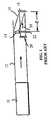
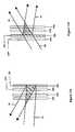
- FIG. 1illustrates one of the simplest geometries for forming a master hologram. This simple configuration illustrates the basic components for simple holographic construction, including a coherent light source 10 emitting an incident beam 12 . From this incident beam 12 , two separate beams are formed.
- a prism 14 or similar light-splitting or directing deviceintercepts part of the incident beam 12 and directs a reference beam 16 to a detector plate 18 . Simultaneously, a part of the incident beam is diffused by a diffusion screen 20 and diffracts off an object 22 , forming an object beam 24 , which also passes onto the detector plate 18 .
- the interaction between the reference beam 16 and the object beam 24produces an off-axis hologram, in the form of multiple Fresnel patterns and interference fringes.
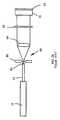
- FIG. 2 arepresents the simplest system and method for duplicating the master hologram.
- an incident beam 12from a coherent light source 10 which forms two separate beams, a reference beam 16 and an object beam 24 .
- object beam 24results from the interaction of part of incident beam 12 with the master hologram 26 .
- the object beamis directed along the formation angle and a detector 18 is placed at the intersection of the reference beam 16 and the object beam 24 , forming a replica of the interference pattern comprising master hologram 26 .
- the object beamforms a virtual image of master hologram 26 which is recorded on the detector 18 .
- the real imageis not used in the reproduction process.
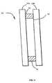
- the prior artalso contemplates a single beam master hologram duplication system that greatly reduces the number of necessary optical components.
- this system for duplicating a master hologramresembles in many respects the art of photography.
- the master hologram and a holographic detection platee.g., emulsion plate
- Photographic development of the holographic detection plateresults in a replica master hologram.
- the optical contact between the master hologram and the holographic detection platemust be such that there is no loss of resolution within the interference fringes.
- Establishing the requisite optical contacthas proved to be a significant limiting factor in attempts to use contact printing for duplication of holograms. Consequently, the prior art single-beam contact printing method, though it reduces the number of optical elements necessary for duplication of a master hologram, poses new optical hurdles to the art of hologram replication.
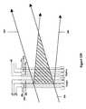
- Brandstettera prior art single beam contact printing system is illustrated in accordance with U.S. Pat. No. 5,547,786 to Brandstetter, et al. (“Brandstetter”), the specification of which is incorporated herein by reference.
- the system of Brandstetterincludes a source of monochromatic, collimated light of substantially fixed wavelength such as laser 10 which produces an output beam 12 , referred to as the replication or recording beam, and directs that beam through beam conditioning means 80 , which preferably comprises lenses 82 and 84 , pinhole 86 , and filter 88 .
- Lenses 82 and 84 and pinhole 86are provided to collimate beam 12 and to expand that beam to the desired size filter 88 is provided to control or adjust the intensity or amplitude of beam 12 across its profile as desired.
- the conditioned beam 12is directed at a desired angle onto master holographic optical element 26 , passes through, and directly enters a phase recording medium 18 , such as a photopolymer layer that has been applied onto the backside of the master holographic optical element.
- the method for forming the replica within the photopolymer layerrequires a polymerization step which is separate from the recording step. Further, the resulting replica hologram is not switchable. Further, the recording mediums currently available as blanks for hologram duplication are limited in their ability to provide optimal optical contact with the master hologram.
- the present inventionoffers increased efficiency and quality in the duplication of a master hologram utilizing an improved method and system of contact printing.
- a first embodiment of an improved method and system of contact printingemploys a polymer-dispersed liquid crystal (PDLC) recording medium as the duplication blank.
- PDLCpolymer-dispersed liquid crystal
- the optical qualities of the PDLC material described hereinprovide an improved method of duplication using single beam contact printing regardless of the material comprising the master hologram.
- master holograms originally recorded using highly complex optical geometriese.g., computer generated holograms
- the improved hologram contact printing method and system described hereinworks with virtually any type of master hologram, including both reflection and transmission holograms.
- a first embodiment of the present inventiondescribes a system for duplicating a hologram which includes a radiation source for emitting a coherent beam of radiation, a hologram, and a recording substrate comprised of a polymer-dispersed liquid crystal material for recording a replica of the hologram therein.
- the components of the systemare arranged such that the hologram and the recording substrate are in optical contact with one another and they are placed in a path of the coherent beam of radiation.
- a second embodiment of the present inventiondescribes a method for duplicating a hologram which includes the following steps of (1) directing a coherent incident radiation beam at a first optical component; (2) transmitting the coherent incident radiation beam through the first optical component forming a transmitted beam, to a second optical component having a hologram recorded therein; and (3) diffracting the transmitted beam via the hologram forming a diffracted radiation beam.
- the incident beam and the diffracted beaminterfere within the first optical component to form a replica of the hologram therein.
- a third embodiment of the present inventiondescribes a method for contact recording at least one hologram which includes the following steps of: (1) directing a coherent radiation beam at a first optical component having a hologram recorded therein and (2) diffracting a first portion and transmitting a second portion of the coherent radiation beam through the first optical component to a second optical component. The transmitted beam and the diffracted beam interfere within the second optical component to form a replica of the hologram therein.
- a fourth embodiment of the present inventiondescribes a method for contact recording at least one hologram which includes the following steps of: (1) optically contacting at least one master hologram to at least one holographic blank to form a master/blank assembly; (2) exposing the master/blank assembly to a pre-recording beam; (3) exposing the master/blank assembly to a recording beam; and (4) exposing the master/blank assembly to a post-recording beam, wherein the master/blank assembly remains optically contacted throughout each exposure.
- a fifth embodiment of the present inventiondescribes a method for contact recording at least one hologram which includes the following steps: (1) optically contacting at least one master hologram to at least one holographic blank to form a master/blank assembly; (2) exposing the master/blank assembly to a recording beam; and (3) exposing the master/blank assembly to a post-recording beam, wherein the master/blank assembly remains optically contacted throughout each exposure.
- a sixth embodiment of the present inventiondescribes a system for contact recording at least one hologram which includes at least one master hologram, at least one holographic blank, a pre-recording beam, and a recording beam, wherein the at least one master hologram and the at least one holographic blank are in optical contact during exposure to the pre-recording beam and the recording beam.
- a seventh embodiment of the present inventiondescribes a system for contact recording at least one hologram which includes at least one master hologram, at least one holographic blank, a recording beam, and a post-recording beam, wherein the at least one master hologram and the at least one holographic blank are in optical contact during exposure to the recording beam and the post-recording beam.
- An eighth embodiment of the present inventiondescribes a system for contact recording at least one hologram which includes at least one master hologram, at least one holographic blank, a pre-recording beam, a recording beam, and a post-recording beam, wherein the at least one master hologram and the at least one holographic blank are in optical contact during exposure to the pre-recording beam, the recording beam, and the post-recording beam.
- FIG. 1is a schematic view of a conventional system for forming a master transmission hologram
- FIG. 2 ais a schematic view of a conventional system for forming a replica of the master hologram of FIG. 1;
- FIG. 2 bis a schematic view of a conventional system for forming a replica hologram via a contact printing method
- FIG. 3is a schematic view of a system according to an embodiment of the present invention for forming a replica hologram in a PDLC blank from a master transmission hologram;
- FIG. 4is a schematic view of a system according to an embodiment of the present invention for forming a replica hologram in a PDLC blank from a master reflection hologram;
- FIG. 5is a schematic view of a PDLC blank according to an embodiment of the present invention for forming a replica hologram therein;
- FIG. 6is a schematic view of a recording system for forming a transmission hologram according to the present invention.
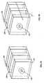
- FIGS. 7 a and 7 bare elevational views of a reflection grating in accordance with the present invention having planes of polymer channels and liquid crystal channels disposed parallel to the front surface, in the absence of a field (FIG. 7 a ) and with an electric field applied (FIG. 7 b ), wherein the liquid crystal utilized in the formation of the grating has a positive dielectric anisotropy;
- FIGS. 8 a and 8 bare elevational views of a reflection grating in accordance with the invention having planes of polymer channels and liquid crystal channels disposed parallel to the front surface of the grating, in the absence of an electric field (FIG. 8 a ) and with an electric field applied (FIG. 8 b ), wherein the liquid crystal utilized in the formation of the grating has a negative dielectric anisotropy;
- FIGS. 9 a , 9 b , 9 c , 9 d , 9 e , and 9 fare pre-recording, exposure, and post-recording views of a contact printing system incorporating a switchable H-PDLC master according to an embodiment of the present invention
- FIGS. 10 a and 10 bare reflection and transmission exposure views wherein a switchable H-PDLC master is partially switched according to an embodiment of the present invention
- FIG(S). 11 ( a )-( b )are multiple beam, multiple master, multiple blank exposure views utilizing a reflective and transmissive switchable H-PDLC master, according to embodiments of the present invention
- FIG(S). 12 ( a )-( b )are multiple beam, multiple master, multiple blank exposure views utilizing reflective and transmissive switchable H-PDLC masters respectively, to form an RGB stacked replica, according to embodiments of the present invention.
- the improved contact printing method and systems described hereincomprise the following basic components: a coherent light source 31 emitting an incident beam 33 , a master hologram 35 emitting diffracted beam 34 and transmitted beam 36 , a polymer-dispersed liquid crystal (“PDLC”) blank 37 for recording a replica of the master hologram, and, optionally, an absorption filter 39 .
- a coherent light source 31emitting an incident beam 33
- a master hologram 35emitting diffracted beam 34 and transmitted beam 36
- PDLCpolymer-dispersed liquid crystal
- absorption filter 39the order and placement of these elements with respect to one another vary depending on whether the master hologram is transmissive or reflective.
- the PDLC materials described hereinmay be used in both the PDLC blank 37 and the master hologram 35 .
- the master hologram 35may be formed on a conventional photographic plate or similar emulsion-type recording medium, or by computer generation, for example.
- the blank 37may be formed of an appropriate photosensitive material as determined by one skilled in the art.
- a blank recording or master hologram mediumcomprised of a PDLC material comprising a monomer, a liquid crystal material, a cross-linking monomer, a coinitiator and a photoinitiator dye.
- PDLC materialsexhibit clear and orderly separation of the liquid crystal and cured polymer, whereby the PDLC material advantageously provides high quality holographic gratings.
- the PDLC materials of the present inventionare also advantageously formed in a single step.
- the present inventionalso utilizes a unique photopolymerizable prepolymer material that permits in situ control of significant characteristics of the resulting gratings, such as domain size, shape, density, ordering, and the like.
- the methods and materials of the present inventioncan be used to prepare PDLC materials that function as switchable transmission or reflection holograms or holographic gratings.
- the PDLC material employed in the practice of the present inventioncreates a switchable hologram in a single step.
- a new feature of a preferred PDLC materialis that illumination by an inhomogeneous, coherent light pattern initiates a patterned, anisotropic diffusion (or counter-diffusion) of polymerizable monomer and second phase material, particularly liquid crystal.
- second phase materialparticularly liquid crystal.
- a resulting preferred PDLC materialhas an anisotropic spatial distribution of phase-separated liquid crystal droplets within the photochemically cured polymer matrix.
- Conventional PDLC materials made by a single-step processcan achieve at best only regions of larger liquid crystal droplets and smaller liquid crystal droplets in a polymer matrix.
- the large bubble sizesare highly scattering, producing a hazy appearance and multiple order diffractions, in contrast to the well-defined first order diffraction and zero order diffraction resulting from the small liquid crystal droplets of the preferred PDLC material in well-defined channels of liquid crystal-rich material.
- the features of the PDLC materialare influenced by the components used in the preparation of the homogeneous starting mixture and, to a lesser extent, by the intensity of the incident light pattern.
- the prepolymer materialcomprises a mixture of a photopolymerizable monomer, a second phase material, a photoinitiator dye, a coinitiator, a chain extender (or cross-linker), and, optionally, a surfactant.
- the two major components of the prepolymer mixtureare the polymerizable monomer and the second phase material, which are preferably completely miscible.
- Highly functionalized monomersare preferred because they form densely cross-linked networks which shrink to some extent and tend to squeeze out the second phase material. As a result, the second phase material is moved anisotropically out of the polymer region and, thereby, separated into well-defined, polymer-poor, second phase-rich regions or domains.
- Highly functionalized monomersare also preferred because the extensive cross-linking associated with such monomers yields fast kinetics, allowing the hologram to form relatively quickly, whereby the second phase material will exist in domains of less than approximately 0.1 ⁇ m.
- Suitable acrylatessuch as triethyleneglycol diacrylate, trimethylolpropane triacrylate, pentaerythritol triacrylate, pentaerythritol tetraacrylate, pentaerythritol pentaacrylate, and the like can be used in the present invention.
- an approximately 1:4 mixture of tri- to penta-acrylatefacilitates homogeneous mixing, while providing a favorable mixture for forming 1-100 ⁇ m thin films on the optical plates.
- the second phase material of choice for use in the practice of the present inventionis a liquid crystal.
- the concentration of liquid crystal employedshould be large enough to allow a significant phase separation to occur in the cured sample, but not so large as to make the sample opaque or very hazy. Below about 20% by weight very little phase separation occurs and diffraction efficiencies are low. Above about 35% by weight, the sample becomes highly scattering, reducing both diffraction efficiency and transmission. Samples fabricated with approximately 25% by weight of liquid crystal typically yield good diffraction efficiency and optical clarity. In prepolymer mixtures utilizing a surfactant, the concentration of liquid crystal may be increased to 35% by weight without loss in optical performance by adjusting the quantity of surfactant.
- Suitable liquid crystals contemplated for use in the practice of the present inventioninclude the mixture of cyanobiphenyls marketed as E7 by Merck, 4′-n-pentyl-4-cyanobiphenyl, 4′-n-heptyl-4-cyanobiphenyl, 4′-octaoxy-4-cyanobiphenyl, 4′-pentyl-4-cyanoterphenyl, 4-methoxybenzylidene-4′-butylaniline, and the like. Other second phase components are also possible.
- a polymer-dispersed liquid crystal material employed in the practice of the present inventionis formed from a prepolymer material that is a homogeneous mixture of a polymerizable monomer comprising dipentaerythritol hydroxypentaacrylate (available, for example, from Polysciences, Inc., Warrington, Pa.), approximately 10-40% by weight of the liquid crystal E7 (which is a mixture of cyanobiphenyls marketed as E7 by Merck and also available from BDH Chemicals, Ltd., London, England), the chain-extending monomer N-vinylpryrrolidone(“NVP”) (available from the Aldrich Chemical Company, Milwaukee, Wis.), coinitiator N-phenylgylycine (“NPG”) (also available from the Aldrich Chemical Company, Milwaukee, Wis.), and the photoinitiator dye rose bengal ester; (2,4,5,7-tetraiodo-3′,4′,5′,6′-te
- FIG. 5A preferred example of a PDLC duplication blank 38 is illustrated in FIG. 5 .
- This cross-sectional view of a duplication blank 38is formed of a layer 50 of the PDLC material sandwiched between a pair of indium-tin-oxide (“ITO”) coated glass slides 52 a and 52 b and spacers 54 .
- ITOindium-tin-oxide
- the master hologram 35is formed from PDLC material.
- the interior of master hologram 35reveals a Bragg transmission grating 56 (FIG. 6) formed when PDLC material layer 50 is exposed to an interference pattern from two intersecting beams of coherent laser light.
- FIG. 6there is shown an exemplary system for recording a master transmission hologram using PDLC materials of the present invention.
- a coherent light source 62(e.g., Ar ion laser) is incident upon a spatial filter 64 and a collimating lens 66 prior to being divided via a dual slit aperture 68 and impinging upon a prism 70 causing the dual beams to interfere within the layer of PDLC material 50 .
- the PDLC materialis sandwiched between layers of ITO glass slides 52 a and 52 b , separated by spacers 54 .
- neutral density filters 57are placed before slide 52 a and after slide 52 b , separated by an index matching fluid 53 .
- electrodes 55are provided in electrical contact with the ITO glass slides 52 a and 52 b .
- electrodes 55are provided in electrical contact with the ITO glass slides 52 a and 52 b .
- the PDLC materialis a mixture of liquid crystal and prepolymer material homogenized to form a viscous solution by suitable means (e.g., ultrasonification) and spread between, for example, ITO coated glass slides with spacers of nominally 1-100 ⁇ m thickness and, preferably, 4-20 ⁇ m thickness.
- the ITOis electrically conductive and serves as an optically transparent electrode. Preparation, mixing and transfer of the prepolymer material onto the glass slides are preferably performed in conditions outside of the absorbance spectrum of the selected photoinitiator dye.
- the sensitivity of the prepolymer materials to lightis dependent on the photoinitiator dye and its concentration. Higher dye concentration leads to higher sensitivity. In most cases, however, the solubility of the photoinitiator dye limits the concentration of the dye and, thus, the sensitivity of the prepolymer material. Nevertheless, it has been found that for most general applications photoinitiator dye concentrations in the range of 0.2-0.4% by weight are sufficient to achieve desirable sensitivities and allow for a complete bleaching of the dye in the recording process, resulting in colorless final samples.
- Photoinitiator dyesthat are useful in generating PDLC materials in accordance with the present invention are rose bengal ester (2,4,5,7-tetraiodo-3′,4′,5′,6′-tetrachlorofluroescein-6-acetate ester); rose bengal sodium salt; eosin; eosin sodium salt; 4,5-diiodosuccinyl fluorescein; camphorquinone; methylene blue; and the like. These dyes allow a sensitivity to recording wavelengths across the visible spectrum from nominally 400 nm to 700 nm.
- Suitable near-infrared dyessuch as cationic cyanine dyes with trialkylborate anions having absorption from 600-900 nm, as well as merocyanine dyes derived from spiropyran, should also find utility in connection with the present invention.
- the coinitiator employed in the practice of the present inventioncontrols the rate of curing in the free radical polymerization reaction of the prepolymer material. Optimum phase separation and, thus, optimum diffraction efficiency in the resulting PDLC material are a function of curing rate. It has been found that favorable results can be achieved utilizing the coinitiator in the range of 2-3% by weight.
- Suitable coinitiatorsinclude N-phenylglycine; triethylene amine; triethanolamine; N,N-dimethyl-2,6-diisopropyl aniline; and the like.
- Suitable dyes and dye-coinitiator combinationsthat should be suitable for use in the present invention, particularly for visible light, include eosin and triethanolamine; camphorquinone and N-phenyglycine; fluorescein and triethanolamine; methylene blue and triethanolamine or N-phenylglycine; erythrosin B and triethanolamine; indolinocarbocyanine and triphenyl borate; iodobenzospiropyran and triethylamine; and the like.
- the chain extender (or cross-linker) employed in the practice of the present inventionhelps to increase the solubility of the components in the prepolymer material, as well as increase the speed of polymerization.
- the chain extenderis preferably a smaller vinyl monomer as compared with the pentaacrylate, whereby it can react with the acrylate positions in the pentaacrylate monomer, which are not easily accessible to neighboring pentaacrylate monomers as a result of steric hindrance.
- reaction of the chain extender monomer with the polymerincreases the propagation length of the growing polymer and results in high molecular weights. It has been found that a chain extender in the range of 10-18% by weight maximizes the performance in terms of diffraction efficiency.
- suitable chain extenderscan be selected from the following: N-vinyl pyrrolidone; N-vinyl pyridine; acrylonitrile; N-vinyl carbazole; and the like.
- a surfactant materialfor example, octanoic acid
- the switching voltage for PDLC materials containing a surfactantare significantly lower than those of a PDLC material made without the surfactant. While not wishing to be bound by any particular theory, it is believed that these results may be attributed to the weakening of the anchoring forces between the polymer and the phase-separated liquid crystal droplets. Scanning electron microscopy (“SEM”) studies have shown that droplet sizes in PDLC materials including surfactants are reduced to the range of 30-50 nm and the distribution is more homogeneous.
- SEMscanning electron microscopy
- Random scattering in such materialsis reduced due to the dominance of smaller droplets, thereby increasing the diffraction efficiency.
- shape of the dropletsbecomes more spherical in the presence of surfactant, thereby contributing to the decrease in switching voltage.
- Suitable surfactantsinclude octanoic acid; heptanoic acid; hexanoic acid; dodecanoic acid; decanoic acid; and the like.
- suitable electrically switchable gratingscan be formed from a polymerizable monomer, vinyl neononanoate (“VN”) C 8 H 17 CO 2 CH ⁇ CH 2 , commercially available from the Aldrich Chemical Co. in Milwaukee, Wisconsin.
- VNvinyl neononanoate
- Showable resultshave also been obtained where the chain extender NVP and the surfactant octanoic acid are replaced by 6.5% by weight VN.
- VNalso acts as a chain extender due to the presence of the reactive acrylate monomer group.
- high optical quality sampleswere obtained with about 70% diffraction efficiency, and the resulting gratings could be electrically switched by an applied field of 6 V/ ⁇ m.
- PDLC materials in accordance with the present inventionmay also be formed using a liquid crystalline bifunctional acrylate as the monomer (“liquid crystal monomer”).
- liquid crystal monomera liquid crystalline bifunctional acrylate as the monomer
- the liquid crystal monomershave an advantage over conventional acrylate monomers due to their high compatibility with the low molecular weight nematic liquid crystal materials, thereby facilitating formation of high concentrations of low molecular weight liquid crystal and yielding a sample with high optical quality.
- the presence of higher concentrations of low molecular weight liquid crystals in the PDLC materialgreatly lowers the switching voltages (e.g., to ⁇ 2 V/ ⁇ m).
- liquid crystal monomersAnother advantage of using liquid crystal monomers is that it is possible to apply low AC or DC fields while recording holograms to pre-align the host liquid crystal monomers and the low molecular weight liquid crystal so that a desired orientation and configuration of the nematic directors can be obtained in the liquid crystal droplets.
- the chemical formulae of several suitable liquid crystal monomersare as follows:
- Semifluorinated polymersare known to show weaker anchoring properties and also significantly reduced switching fields. Thus, it is believed that semifluorinated acrylate monomers, which are bifunctional and liquid crystalline will find suitable application in the present invention.
- the prepolymer material utilized to make a reflection gratingcomprises a monomer, a liquid crystal, a cross-linking monomer, a coinitiator, and a photoinitiator dye.
- the reflection gratingis formed from prepolymer material comprising by total weight the monomer dipentaerythritol hydroxypentaacrylate (“DPHPA”), 34% by total weight of a liquid crystal comprising a mixture of cyano biphenyls (known commercially as “E7”), 10% by total weight of a cross-linking monomer comprising NVP, 2.5% by weight of the coinitiator N-phenylglycine (“NPG”), and 10 ⁇ 5 to 10 ⁇ 6 gram moles of a photoinitiator dye comprising rose bengal ester.
- DPHPAmonomer dipentaerythritol hydroxypentaacrylate
- E7cyano biphenyls
- NVPcoinitiator N-phenylgly
- grating 130includes periodic planes of polymer channels 130 a and PDLC channels 130 b which run parallel to the front surface 134 .
- the grating spacing associated with these periodic planesremains relatively constant throughout the full thickness of the sample from the air/film to the film/substrate interface.
- the morphology of the reflection gratingdiffers significantly.
- the droplets that were present in the materialwere significantly smaller, having diameters between 50 and 100 nm.
- the liquid crystal-rich component of a reflection gratingis significantly larger.
- a periodic refractive index modulationis disposed through the thickness of the film.
- a resulting reflection notchmay have a reflection wavelength at approximately 472 nm for normal incidence and a relatively narrow bandwidth. This small difference between the writing wavelength and the reflection wavelength (approximately 3%) indicates that shrinkage of the film is not a significant problem under these exemplary conditions.
- multiple write/reflect conditionsare easily obtainable according to desired specifications and manipulations and adjustments to the recording geometry may also account for shrinkage, thus minimizing any resulting negative effects.
- the performance of such gratingsis stable over periods of many months.
- suitable PDLC materialscould be prepared utilizing monomers such as triethyleneglycol diacrylate, trimethylolpropane triacrylate, pentaerythritol triacrylate, pentaerythritol tetraacrylate, pentaerythritol pentaacrylate, and the like.
- monomerssuch as triethyleneglycol diacrylate, trimethylolpropane triacrylate, pentaerythritol triacrylate, pentaerythritol tetraacrylate, pentaerythritol pentaacrylate, and the like.
- other coinitiatorssuch as triethylamine, triethanolamine, N,N-dimethyl-2,6-diisopropylaniline, and the like could be used instead of N-phenylglycine.
- the photoinitiator dyesrose bengal sodium salt, eosin, eosin sodium salt, fluorescein sodium salt and the like will give favorable results.
- the 633 nm lineis utilized, methylene blue will find ready application.
- other liquid crystalssuch as 4′-pentyl-4-cyanobiphenyl or 4′-heptyl-4-cyanobiphenyl, can be utilized in accordance with the invention.
- FIG. 7 athere is shown an elevational view of a reflection grating 130 in accordance with the invention having periodic planes of polymer channels 130 a and PDLC channels 130 b disposed parallel to the front surface 134 of the grating 130 .
- the symmetry axis 136 of the liquid crystal domainsis formed in a direction perpendicular to the periodic channels 130 a and 130 b of the grating 130 and perpendicular to the front surface 134 of the grating 130 .
- the symmetry axis 136is already in a low energy state in alignment with the field E and will not reorient.
- reflection gratings formed in accordance with the procedure described abovewill not normally be switchable.
- a reflection gratingtends to reflect a narrow wavelength band, such that the grating can be used as a reflection filter.
- the reflection gratingis formed so that it will be switchable.
- switchable reflection gratingscan be made utilizing negative dielectric anisotropy liquid crystals (or liquid crystals with a low cross-over frequency), an applied magnetic field, an applied shear stress field, or slanted gratings.
- liquid crystals having a negative dielectric anisotropywill rotate in a direction perpendicular to an applied field.
- the symmetry axis 136 of the liquid crystal domains formed with a liquid crystal having a negative ⁇will also be disposed in a direction perpendicular to the periodic channels 130 a and 130 b of the grating 130 and to the front surface 134 of the grating.
- an electric field Eis applied across such gratings, as shown in FIG.
- the symmetry axis of the negative ⁇ liquid crystalwill distort and reorient in a direction perpendicular to the field E, which is perpendicular to the film and the periodic planes of the grating.
- the reflection gratingcan be switched between a state where it is reflective and a state where it is transmissive.
- Liquid crystalscan be found in nature (or synthesized) with either positive or negative ⁇ . Thus, in more detailed aspects of the invention, it is possible to use a liquid crystal which has a positive ⁇ at low frequencies, but becomes negative at high frequencies.
- the frequency (of the applied voltage) at which ⁇ changes signis called the cross-over frequency.
- the cross-over frequencywill vary with liquid crystal composition, and typical values range from 1-10 kHz. Thus, by operating at the proper frequency, the reflection grating may be switched.
- low cross-over frequency materialscan be prepared from a combination of positive and negative dielectric anisotropy liquid crystal.
- a suitable positive dielectric liquid crystal for use in such a combinationcontains four ring esters as shown below:
- a strongly negative dielectric liquid crystal suitable for use in such a combinationis made up of pyridazines as shown below:
- liquid crystal materialsare available from LaRoche & Co., Switzerland. By varying the proportion of the positive and negative liquid crystals in the combination, crossover frequencies from 1.4-2.3 kHz are obtained at room temperature.
- Another combination suitable for use in the present embodimentis a combination of the following: p-pentylphenyl-2-chloro-4-(p-pentylbenzoyloxy) benzoate and 4-(p-pentylbenzoyloxy) benzoate and p-heptylphenyl-2-chloro-4-(p-octylbenzoyloxy) benzoate. These materials are available from Kodak® Company.
- a system 30 for reproducing a switchable transmission hologram from a master hologram 35is shown.
- the master hologram 35is mounted in the path of an incident beam 33 at the Bragg angle.
- a PDLC blank 37is optically contacted to the master hologram 35 at the same angle to form a master/blank assembly.
- an absorption filter 30e.g., neutral density
- the master/blank assembly of master hologram 35 , PDLC blank 37 , and, optionally, absorption filter 30is then illuminated using a single coherent incident beam 33 from radiation source 31 .
- the radiation source 31emits a coherent radiation beam 33 (e.g., laser) that is directed towards a first surface of the master hologram 35 .
- a coherent radiation beam 33e.g., laser
- part of incident beam 33is diffracted by the holographic grating 56 , forming diffracted beam 34
- part of the incident beam 33is transmitted undiffracted, forming transmitted beam 36 .
- Both diffracted beam 34 and transmitted beam 36pass through the second surface of the master hologram 35 and into the optically contacted first surface of the PDLC blank 37 .
- the transmitted beam 36 and the diffracted beam 34interfere, forming a replica of holographic grating 56 therein.
- FIG. 4a system 40 for reproducing reflection holograms according to an embodiment of the present invention is shown. While similar to the transmission reproduction system 30 of FIG. 3, the reflection reproduction system 40 requires that PDLC blank 37 be located before the master hologram 35 within the optical path, followed by an absorption filter 39 . As in FIG. 3, the PDLC blank 37 , master hologram 35 and filter 39 configuration is oriented at the Bragg angle with respect to the coherent incident beam 33 from radiation source 31 .
- the radiation source 31emits a coherent radiation beam 33 (e.g., laser) that is directed towards a first surface of the PDLC blank 37 .
- the incident beam 33is transmitted through the PDLC blank 37 as transmitted beam 36 , passing through the second surface thereof and enters the first surface of the master hologram 35 which is optically contacted to the second surface of the PDLC blank 37 .
- the incident beam 33is diffracted by the holographic grating 56 located therein, creating diffracted beam 34 .
- Transmitted beam 36 and diffracted beam 34interfere within the PDLC blank 37 forming a replica of holographic grating 56 therein.
- the master hologramis not limited to a PDLC hologram.
- the master hologrammay be, but is not limited to, a computer generated hologram, any of a variety of emulsion-type holograms, a photopolymer hologram, a photochromic hologram, a polymer dispersed liquid crystal hologram, silver halide photographic emulsion hologram, dichromated gelatin hologram, photoresist hologram, photothermoplastic hologram, photorefractive crystal hologram, multiplexed hologram, white light hologram, rainbow hologram, thin holograms, in-line hologram, off-axis hologram, fourier hologram, fraunhofer hologram, diffractive optical element (DOE), holographic optical element (HOE), evanescent-wave hologram, image hologram, amplitude hologram, phase hologram, volume hologram, surface hologram, transmission
- DOEdiffractive
- electrodesmay be attached to ITO glass slides (as described in FIG. 6) of either one or the other or both the master hologram 35 and the PDLC blank 37 .
- the replica hologramsmay be formed so as to diffract either with the application of a specified voltage or in the absence of the application of a specified voltage, in order to meet design and system specifications.
- H-PDLCswitchable holographic-PDLC
- the blanksare not restricted to the PDLC material described herein.
- One skilled in the artrecognizes the alternative materials which may be used for the replica in the proceeding embodiments of the present invention.
- the blankis exposed prior to recording in order to improve uniformity of the hologram and for aesthetic reasons.
- Pre-recordingin this context means prior to exposure of the H-PDLC master.
- pre-recording irradiationis necessary based on the composition of the blank.
- the master and the blankare in close physical and optical proximity. If the master hologram is not capable of being switched OFF, any exposure radiation through the master hologram, will necessarily cause a pattern to be created within the blank. But, in the case where the master hologram is an H-PDLC master, the holographic nature of the master may actually be turned OFF and ON under electrical control, such that in the OFF state, the H-PDLC master resembles a piece of transparent glass as shown in FIG. 9 a . In FIG.
- the H-PDLC master reflection hologram 35is turned OFF, such that the liquid crystals do not orient so as to form a holographic grating within the H-PDLC master. Consequently, a pre-recording beam 5 passes through the PDLC blank 37 and the H-PDLC master 35 without being reflected back through the PDLC blank and forming an interference pattern therein.
- a transmission H-PDLC masteras shown in FIG. 9 d the order of the PDLC blank 37 and the H-PDLC master 35 is reversed, such that the pre-recording beam 5 first passes through the master 35 which is OFF and then passes through the blank 37 , without forming any interference pattern with in the blank 37 .
- Pre-recording beam 5may be the same beam as recording incident beam 33 or it may be an auxiliary beam.
- post-recording irradiationmay also be advantageous for certain contact replication scenarios.
- Post-recording exposureis useful with certain recording photopolymer materials (see e.g., Chemistry of Materials) for eliminating unconverted monomers and bleaching unconsumed photosensitive dye.
- certain recording photopolymer materialssee e.g., Chemistry of Materials
- a reflection H-PDLC master 35is ON when incoming beam 33 is incident thereon and is reflected as beam 34 so as to interfere within the blank 37 with incident beam 33 , forming an interference region therein.
- the master hologram 35is turned OFF and a post-recording beam 6 is incident upon what is now the replica of the master but, for simplicity, what we will continue to refer to as the blank 37 but, is not reflected back through by the master 35 because the grating therein is not ON (see FIG. 9 c ).
- post-recordingmay also take place when replicating a transmission hologram.
- replication of a transmission master 35occurs when an incident beam 33 passes through an ON master 35 , wherein part of the incident beam is deflected by the hologram pattern formed therein resulting in diffracted beam 34 . Beams 33 and 34 interfere within the blank 37 to form a replica of the hologram pattern of the master 35 . After this replication step has occurred, it is preferable in some situations to irradiate the now replica (used to be blank) 37 with a post-recording beam 6 as shown in FIG. 9 f .
- Post-recording beam 6may be the same beam as recording incident beam 33 or it may be an auxiliary beam.
- Both the pre-recording and the post-recording embodiments utilizing the H-PDLC masterimprove the efficiency of contact printing. Without the benefit of the switchable master, there are significant physical changes to the printing component which must occur before and after the actual exposure. First, the blank would have to be pre-exposed without being in optical contact with the master, next for the recording step, the master would have to be optically contacted thereto, and finally, for post-recording, the master would have to be removed from the blank (now replica) prior to irradiation of the blank with the post-recording beam. These multiple configurations for pre-recording exposure, recording exposure, and post-recording exposure add significant time to the contact printing process and reduce efficiency. Using the H-PDLC master, allows for a single configuration during the performance of all three exposure steps.
- using a switchable H-PDLC masterallows for substantial control of diffraction efficiency.
- the incident beamis split into two beams, a transmitted beam and a diffracted beam.
- the optimum beam balance between the transmitted and diffracted beamsis often 1:1 since the beams are overlapping to form the replica holographic transmission grating within the blank.
- the diffraction efficiencymay not be selectively turned OFF and ON and it is not variable. Consequently, given a static hologram which does not meet the 1:1 requirement, there is a limitation in the quality of the replica due to the non-optimal diffraction efficiency.
- the diffraction efficiencyis voltage controlled. Consequently, the optimum efficiency can in effect be tuned in. This ability to change or tune the diffraction efficiency in order to achieve the optimal 1:1 power ratio is extremely useful where the hologram to be replicated is complex. For example, where the master hologram is a lens or some other complicated fringe pattern, the diffraction efficiency may be manipulated in order to find the beam ratio, be it 1:1 or otherwise, that produces the replica with highest fidelity.
- incident recording beam 33is split into transmitted beam 36 and diffracted beam 34 by only partially switching the master H-PDLC hologram 35 .
- the ability to partially switch the masteris analogized to an analog signal as opposed to a digital signal. Instead of choosing from two states, all ON or all OFF, a partially switchable H-PDLC master allows for a range of diffraction efficiencies. For example, as the applied voltage varies through a range, the diffraction efficiency of the master also varies through a range.
- a reflective masteris contact printed when the incident beam 33 and the diffracted beam 34 interfere within the blank 37 .
- the power of the diffracted beammay be varied with voltage as desired.
- the transmitted beam 36 and the diffracted beam 34interfere within the blank 37 and both the transmitted beam power and the diffracted beam power are capable of voltage control.
- the switchable H-PDLC masteris utilized in order to create replica holograms with tailored diffraction efficiency through decreased fringe contrast.
- holographic exposure with low fringe contrastwill result in a replica with less than optimum diffraction efficiency.
- the writing beamsbecome imbalanced (or the optimum balance for the system is altered) and thus a decreased replica diffraction efficiency results.
- a power ratio other than 1:1is desired during the replication process (see e.g., D. J. Lougnot et al., “Photopolymers for Holographic Recording: IV.
- a single switchable H-PDLC masteris able to produce multiple replicated static holograms with identical prescriptions but with various diffraction efficiencies. Without the partial switching capability of the H-PDLC master, multiple static masters with varying photopolymer recipes must be used to create this result. This method and system are cumbersome and inefficient. Additionally, decreased diffraction efficiency can also be achieved by decreasing the overall incident power. However, the total incident power in that case would not be maintained so as to preserve reaction rates within the blank. This embodiment of the present invention preserves the total power incident on the blank to preserve reaction rates.
- FIG. 11 ( a )when contact printing multiple reflection masters in accordance with a preferred embodiment of the present invention, the first replica lens 37 a is recorded with the first master 35 a switched ON and the second master 35 b switched OFF (not shown).
- the second replica lens 37 bis recorded with the second master 35 b switched ON and the first master 35 a switched OFF.
- the first replica lens 37 ais recorded with the first master 35 a switched ON and the second master 35 b switched OFF (not shown).
- the second replica lens 37 bis recorded with the second master 35 b switched ON and the first master 35 a switched OFF.
- FIG(s) 11 ( a )-( b )Another preferred embodiment of the present invention is a system and method for mass producing a Red-Green-Blue (RGB) holographic lens stack according to the principles illustrated with regard to FIG(s) 11 ( a )-( b ).
- Holographic lenseshave unique applications in the art of personal displays in that their optical properties cannot be reproduced with conventional refractive optics. In such personal displays a color image is produced by rapidly sequencing independent red, green, and blue images. To avoid color cross talk and interference, switchable H-PDLC lenses are employed, allowing only the appropriate color hologram(s) to be ON during the RGB sequence. Precise registration of the RGB H-PDLC stack is required so that the three monochrome images overlap.
- a master set of hologramsis designed, recorded, and registered into a master switchable holographic stack, taking into account the required replica optical design, registration, blank substrate dimensions, etc.
- a fixtureis provided to hold the master and replica stacks in optical contact.
- stable, optically clean and uniform laser beams of three different wavelengthse.g., red, green, blue
- the angle of incidence of each of the RGB beams onto the master/replica assemblyis set according to the master designs.
- FIG. 12 ( a )a stack of reflective RGB H-PDLC masters is contact printed.
- a pre-recording irradiationis performed while all masters and blanks are OFF, utilizing the blue laser beam or an appropriate auxiliary beam.
- the green blank 37 bis pre-exposed (if necessary) utilizing the green laser or an auxiliary beam, while all masters, the red and green blanks, and the blue replica are switched OFF.
- FIG. 12 ( a )while recording the green H-PDLC master 35 b utilizing green incident beam 33 b , the blue and red masters 35 a , 35 c , the red and green blanks 37 b , 37 c , and the blue replica 37 a , remain switched OFF, while the green master 35 b is switched ON.
- Green incident beam 33 b and diffracted beam 34 binterfere within the green blank 37 b to form the replica.
- all masters, the red blank, and the blue and green replicasare switched OFF while the green replica is irradiated with the green laser or an auxiliary beam.
- the red blank 37 cis pre-exposed (if necessary) utilizing the red laser or an auxiliary beam, while all masters, the red blank, and the blue and green replicas are switched OFF. While recording the red H-PDLC master 35 c utilizing the red laser, the blue and green masters, the red blank, and the blue and green replicas, remain switched OFF, while the red master 35 c is switched ON. Following the recording step, if post-recording exposure is necessary, all masters and the blue, green, and red replicas are switched OFF while the red replica is irradiated with the red laser or an auxiliary beam.
- the sequence described aboveis applicable. The only difference lies in the interacting beams used to form the interference pattern within the appropriate blank during the recording step. For example, referring to FIG. 12 ( b ), while recording the green H-PDLC master 35 b utilizing green incident beam 33 b , the blue and red masters 35 a , 35 c , the red and green blanks 37 b , 37 c , and the blue replica 37 a , remain switched OFF, while the green master 35 b is switched ON. Unlike in the reflection recording step, the diffracted beam 34 b and the transmitted beam 36 b interfere within the green blank 37 b to form the replica.
- the replica PDLC holograms resulting from the systems and methods described abovebecause of the switching properties of the liquid crystal component of the PDLC material, may be switched accordingly from a diffractive to a transmissive state. Consequently, the duplication method described above allows for increased efficiency and reproducibility of switchable holographic elements. These switchable holographic elements find use in all areas of technology utilizing optical switches including the telecommunications and imaging technologies.
Landscapes
- Physics & Mathematics (AREA)
- General Physics & Mathematics (AREA)
- Chemical & Material Sciences (AREA)
- Nonlinear Science (AREA)
- Dispersion Chemistry (AREA)
- Mathematical Physics (AREA)
- Crystallography & Structural Chemistry (AREA)
- Optics & Photonics (AREA)
- Holo Graphy (AREA)
Abstract
Description


| TABLE 1 |
| Sample Switching Sequence in an RGB Stack |
| Produced by Contact Holography |
| Red | Green | Blue | |||||
| Blank/ | Blank/ | Blank/ | Red | Green | Blue | ||
| Replica | Replica | Replica | Master | Master | Master | ||
| Pre-ex Blue | N/A | N/A | N/A | Off | Off | Off |
| Expose Blue | N/A | N/A | N/A | Off | Off | ON |
| Post-ex Blue | N/A | N/A | N/A | Off | Off | Off |
| Pre-ex Green | N/A | N/A | Off | Off | Off | Off |
| Expose | N/A | N/A | Off | Off | ON | Off |
| Green | ||||||
| Post-ex | N/A | N/A | Off | Off | Off | Off |
| Green | ||||||
| Pre-ex Red | N/A | Off | Off | Off | Off | Off |
| Expose Red | N/A | Off | Off | ON | Off | Off |
| Post-ex Red | N/A | Off | Off | Off | Off | Off |
Claims (9)
Priority Applications (4)
| Application Number | Priority Date | Filing Date | Title |
|---|---|---|---|
| US09/577,166US6730442B1 (en) | 2000-05-24 | 2000-05-24 | System and method for replicating volume holograms |
| PCT/US2001/040691WO2001090822A1 (en) | 2000-05-24 | 2001-05-09 | A system and method for replicating volume holograms |
| AU2001261829AAU2001261829A1 (en) | 2000-05-24 | 2001-05-09 | A system and method for replicating volume holograms |
| US10/796,071US20040175627A1 (en) | 2000-05-24 | 2004-03-10 | System and method for replicating volume holograms |
Applications Claiming Priority (1)
| Application Number | Priority Date | Filing Date | Title |
|---|---|---|---|
| US09/577,166US6730442B1 (en) | 2000-05-24 | 2000-05-24 | System and method for replicating volume holograms |
Related Child Applications (1)
| Application Number | Title | Priority Date | Filing Date |
|---|---|---|---|
| US10/796,071ContinuationUS20040175627A1 (en) | 2000-05-24 | 2004-03-10 | System and method for replicating volume holograms |
Publications (1)
| Publication Number | Publication Date |
|---|---|
| US6730442B1true US6730442B1 (en) | 2004-05-04 |
Family
ID=24307532
Family Applications (2)
| Application Number | Title | Priority Date | Filing Date |
|---|---|---|---|
| US09/577,166Expired - LifetimeUS6730442B1 (en) | 2000-05-24 | 2000-05-24 | System and method for replicating volume holograms |
| US10/796,071AbandonedUS20040175627A1 (en) | 2000-05-24 | 2004-03-10 | System and method for replicating volume holograms |
Family Applications After (1)
| Application Number | Title | Priority Date | Filing Date |
|---|---|---|---|
| US10/796,071AbandonedUS20040175627A1 (en) | 2000-05-24 | 2004-03-10 | System and method for replicating volume holograms |
Country Status (3)
| Country | Link |
|---|---|
| US (2) | US6730442B1 (en) |
| AU (1) | AU2001261829A1 (en) |
| WO (1) | WO2001090822A1 (en) |
Cited By (63)
| Publication number | Priority date | Publication date | Assignee | Title |
|---|---|---|---|---|
| US20040175627A1 (en)* | 2000-05-24 | 2004-09-09 | Sutherland Richard L. | System and method for replicating volume holograms |
| US20040213133A1 (en)* | 2003-04-24 | 2004-10-28 | Hiroyoshi Funato | Diffraction grating, method of producing it, method of duplicating it, optical head device employing it and optical disk drive apparatus employing the optical head device |
| US20050259299A1 (en)* | 2002-04-26 | 2005-11-24 | Discovision Associated | Fast duplication of diffractive storage device for mass production |
| US20060002274A1 (en)* | 2004-06-30 | 2006-01-05 | Sony Corporation | Hologram duplication method |
| US20060275670A1 (en)* | 2005-05-26 | 2006-12-07 | Inphase Technologies, Inc. | Post-curing of holographic media |
| US20060281021A1 (en)* | 2005-05-26 | 2006-12-14 | Inphase Technologies, Inc. | Illuminative treatment of holographic media |
| EP1837870A1 (en)* | 2006-03-20 | 2007-09-26 | Deutsche Thomson-Brandt Gmbh | Pre-exposure and curing of photo-sensitive material for optical data storage |
| US20070223074A1 (en)* | 2005-07-26 | 2007-09-27 | Harris Ken R | Hybrid reflection hologram |
| US20080131626A1 (en)* | 2005-02-09 | 2008-06-05 | Bastiaansen Cees C | Process for Preparing a Polymeric Relief Structure |
| US20080151250A1 (en)* | 2006-12-21 | 2008-06-26 | Seiko Epson Corporation | Lighting device and optical apparatus |
| US20080247011A1 (en)* | 2005-03-16 | 2008-10-09 | General Electric Company | Data storage method and device |
| US20090121747A1 (en)* | 2007-11-12 | 2009-05-14 | Sang Hoo Dhong | Maintaining Circuit Delay Characteristics During Power Management Mode |
| US20090295910A1 (en)* | 2005-03-24 | 2009-12-03 | Jose Mir | Hyperspectral Imaging System and Methods Thereof |
| US20100073745A1 (en)* | 2006-11-13 | 2010-03-25 | Dai Nippon Printing Co., Ltd | Hologram fabrication process, and hologram fabricated by that process |
| US20100188716A1 (en)* | 2007-08-20 | 2010-07-29 | Fujitsu Limited | Hologram recording device |
| US20140141359A1 (en)* | 2002-03-15 | 2014-05-22 | Pd-Ld, Inc. | Methods for manufacturing volume bragg elements |
| US10089516B2 (en) | 2013-07-31 | 2018-10-02 | Digilens, Inc. | Method and apparatus for contact image sensing |
| US10145533B2 (en) | 2005-11-11 | 2018-12-04 | Digilens, Inc. | Compact holographic illumination device |
| US10156681B2 (en) | 2015-02-12 | 2018-12-18 | Digilens Inc. | Waveguide grating device |
| US10185154B2 (en) | 2011-04-07 | 2019-01-22 | Digilens, Inc. | Laser despeckler based on angular diversity |
| US10209517B2 (en) | 2013-05-20 | 2019-02-19 | Digilens, Inc. | Holographic waveguide eye tracker |
| US10216061B2 (en) | 2012-01-06 | 2019-02-26 | Digilens, Inc. | Contact image sensor using switchable bragg gratings |
| US10234696B2 (en) | 2007-07-26 | 2019-03-19 | Digilens, Inc. | Optical apparatus for recording a holographic device and method of recording |
| US10241330B2 (en) | 2014-09-19 | 2019-03-26 | Digilens, Inc. | Method and apparatus for generating input images for holographic waveguide displays |
| US10330777B2 (en) | 2015-01-20 | 2019-06-25 | Digilens Inc. | Holographic waveguide lidar |
| US10359736B2 (en) | 2014-08-08 | 2019-07-23 | Digilens Inc. | Method for holographic mastering and replication |
| US10423222B2 (en) | 2014-09-26 | 2019-09-24 | Digilens Inc. | Holographic waveguide optical tracker |
| US10437051B2 (en) | 2012-05-11 | 2019-10-08 | Digilens Inc. | Apparatus for eye tracking |
| US10437064B2 (en) | 2015-01-12 | 2019-10-08 | Digilens Inc. | Environmentally isolated waveguide display |
| US10459145B2 (en) | 2015-03-16 | 2019-10-29 | Digilens Inc. | Waveguide device incorporating a light pipe |
| US10545346B2 (en) | 2017-01-05 | 2020-01-28 | Digilens Inc. | Wearable heads up displays |
| US10591756B2 (en) | 2015-03-31 | 2020-03-17 | Digilens Inc. | Method and apparatus for contact image sensing |
| US10642058B2 (en) | 2011-08-24 | 2020-05-05 | Digilens Inc. | Wearable data display |
| US10670876B2 (en) | 2011-08-24 | 2020-06-02 | Digilens Inc. | Waveguide laser illuminator incorporating a despeckler |
| US10678053B2 (en) | 2009-04-27 | 2020-06-09 | Digilens Inc. | Diffractive projection apparatus |
| US10690916B2 (en) | 2015-10-05 | 2020-06-23 | Digilens Inc. | Apparatus for providing waveguide displays with two-dimensional pupil expansion |
| US10690851B2 (en) | 2018-03-16 | 2020-06-23 | Digilens Inc. | Holographic waveguides incorporating birefringence control and methods for their fabrication |
| US10732569B2 (en) | 2018-01-08 | 2020-08-04 | Digilens Inc. | Systems and methods for high-throughput recording of holographic gratings in waveguide cells |
| US10859768B2 (en) | 2016-03-24 | 2020-12-08 | Digilens Inc. | Method and apparatus for providing a polarization selective holographic waveguide device |
| US10890707B2 (en) | 2016-04-11 | 2021-01-12 | Digilens Inc. | Holographic waveguide apparatus for structured light projection |
| US10914950B2 (en) | 2018-01-08 | 2021-02-09 | Digilens Inc. | Waveguide architectures and related methods of manufacturing |
| US10942430B2 (en) | 2017-10-16 | 2021-03-09 | Digilens Inc. | Systems and methods for multiplying the image resolution of a pixelated display |
| US10983340B2 (en) | 2016-02-04 | 2021-04-20 | Digilens Inc. | Holographic waveguide optical tracker |
| US11307432B2 (en) | 2014-08-08 | 2022-04-19 | Digilens Inc. | Waveguide laser illuminator incorporating a Despeckler |
| US11378732B2 (en) | 2019-03-12 | 2022-07-05 | DigLens Inc. | Holographic waveguide backlight and related methods of manufacturing |
| US11402801B2 (en) | 2018-07-25 | 2022-08-02 | Digilens Inc. | Systems and methods for fabricating a multilayer optical structure |
| US11442222B2 (en) | 2019-08-29 | 2022-09-13 | Digilens Inc. | Evacuated gratings and methods of manufacturing |
| US11448937B2 (en) | 2012-11-16 | 2022-09-20 | Digilens Inc. | Transparent waveguide display for tiling a display having plural optical powers using overlapping and offset FOV tiles |
| US11460621B2 (en) | 2012-04-25 | 2022-10-04 | Rockwell Collins, Inc. | Holographic wide angle display |
| US11480788B2 (en) | 2015-01-12 | 2022-10-25 | Digilens Inc. | Light field displays incorporating holographic waveguides |
| US11513350B2 (en) | 2016-12-02 | 2022-11-29 | Digilens Inc. | Waveguide device with uniform output illumination |
| US11543594B2 (en) | 2019-02-15 | 2023-01-03 | Digilens Inc. | Methods and apparatuses for providing a holographic waveguide display using integrated gratings |
| US11681143B2 (en) | 2019-07-29 | 2023-06-20 | Digilens Inc. | Methods and apparatus for multiplying the image resolution and field-of-view of a pixelated display |
| US11726332B2 (en) | 2009-04-27 | 2023-08-15 | Digilens Inc. | Diffractive projection apparatus |
| US11747568B2 (en) | 2019-06-07 | 2023-09-05 | Digilens Inc. | Waveguides incorporating transmissive and reflective gratings and related methods of manufacturing |
| US12092914B2 (en) | 2018-01-08 | 2024-09-17 | Digilens Inc. | Systems and methods for manufacturing waveguide cells |
| US12140764B2 (en) | 2019-02-15 | 2024-11-12 | Digilens Inc. | Wide angle waveguide display |
| US12158612B2 (en) | 2021-03-05 | 2024-12-03 | Digilens Inc. | Evacuated periodic structures and methods of manufacturing |
| US12210153B2 (en) | 2019-01-14 | 2025-01-28 | Digilens Inc. | Holographic waveguide display with light control layer |
| US12222499B2 (en) | 2020-12-21 | 2025-02-11 | Digilens Inc. | Eye glow suppression in waveguide based displays |
| US12306585B2 (en) | 2018-01-08 | 2025-05-20 | Digilens Inc. | Methods for fabricating optical waveguides |
| US12399326B2 (en) | 2021-01-07 | 2025-08-26 | Digilens Inc. | Grating structures for color waveguides |
| US12397477B2 (en) | 2019-02-05 | 2025-08-26 | Digilens Inc. | Methods for compensating for optical surface nonuniformity |
Families Citing this family (14)
| Publication number | Priority date | Publication date | Assignee | Title |
|---|---|---|---|---|
| US6998196B2 (en) | 2001-12-28 | 2006-02-14 | Wavefront Technology | Diffractive optical element and method of manufacture |
| US6950173B1 (en) | 2003-04-08 | 2005-09-27 | Science Applications International Corporation | Optimizing performance parameters for switchable polymer dispersed liquid crystal optical elements |
| US7885164B2 (en)* | 2003-10-21 | 2011-02-08 | Optware Corporation | Optical information recording method and optical information recording medium |
| KR100600309B1 (en)* | 2004-06-04 | 2006-07-14 | 주식회사 대우일렉트로닉스 | Data recording / reproducing apparatus using reflective hologram and method thereof |
| DE102005029853B4 (en)* | 2005-06-27 | 2007-05-31 | Prüfbau Dr.-Ing. H. Dürner GmbH | Apparatus for producing a reflection hologram |
| DE102007025907A1 (en)* | 2007-06-01 | 2008-12-11 | Hologram Industries Research Gmbh | Method for producing a multicolor volume hologram, document with such a hologram and volume hologram master |
| DE102010008342A1 (en)* | 2010-02-17 | 2011-08-18 | Jos. Schneider Optische Werke GmbH, 55543 | imaging system |
| CN102279557B (en)* | 2011-07-26 | 2013-10-30 | 华中科技大学 | Method for preparing colour three-dimensional hologram based on holographic polymer dispersed liquid crystal grating |
| EP2862026A1 (en)* | 2012-06-18 | 2015-04-22 | Milan Momcilo Popovich | Apparatus for copying a hologram |
| US20160342001A1 (en)* | 2014-11-11 | 2016-11-24 | Shenzhen China Star Optoelectronics Technology Co., Ltd. | Holographic panel, manufacture method thereof and full color coherent backlight device |
| US20180246354A1 (en)* | 2015-02-23 | 2018-08-30 | Digilens, Inc. | Electrically focus-tunable lens |
| WO2019217409A1 (en)* | 2018-05-07 | 2019-11-14 | Arizona Board Of Regents On Behalf Of The University Of Arizona | Fabrication and replication of volume holographic optical elements |
| US10599097B2 (en) | 2018-05-25 | 2020-03-24 | International Business Machines Corporation | Image and/or video capture from different viewing angles of projected mirror like reflective holographic image surface |
| US12332468B2 (en) | 2020-06-22 | 2025-06-17 | Arizona Board Of Regents On Behalf Of The University Of Arizona | Systems and methods for manufacturing and replicating holographic optical elements and holographic waveguide couplers |
Citations (111)
| Publication number | Priority date | Publication date | Assignee | Title |
|---|---|---|---|---|
| US3580655A (en) | 1964-04-23 | 1971-05-25 | Battelle Development Corp | Wavefront reconstruction |
| US3658526A (en) | 1969-08-25 | 1972-04-25 | Du Pont | Hologram recording in photopolymerizable layers |
| US3667946A (en)* | 1970-09-23 | 1972-06-06 | Holotron Corp | Surface treatment of photopolymer film used for recording holograms |
| US3694218A (en)* | 1970-03-03 | 1972-09-26 | Hughes Aircraft Co | Method of hologram recording |
| US3758186A (en) | 1966-11-30 | 1973-09-11 | Battelle Development Corp | Method of copying holograms |
| US4003629A (en) | 1974-07-17 | 1977-01-18 | Siemens Aktiengesellschaft | Coupling device for light waves |
| US4006963A (en) | 1974-09-06 | 1977-02-08 | Siemens Aktiengesellschaft | Controllable, electro-optical grating coupler |
| US4018228A (en) | 1975-02-24 | 1977-04-19 | Goosen Carl C | Surgical punch apparatus |
| US4045124A (en) | 1975-02-25 | 1977-08-30 | Xerox Corporation | Bistable deflection system |
| US4124947A (en) | 1975-11-14 | 1978-11-14 | Adolf Kuhl | Graphic pattern or the like and method of producing the same |
| US4210132A (en) | 1978-07-26 | 1980-07-01 | The Kendall Company | Artificial sphincter |
| US4368736A (en) | 1980-11-17 | 1983-01-18 | Kaster Robert L | Anastomotic fitting |
| US4374371A (en) | 1980-01-17 | 1983-02-15 | Kearney-National, Inc. | Cadmium electric fuse |
| EP0087281A1 (en)* | 1982-02-23 | 1983-08-31 | Fujitsu Limited | Method of constructing holograms |
| US4416540A (en) | 1981-11-23 | 1983-11-22 | Peter Nicholson | Apparatus and method for holographic contact copying |
| JPS60189729A (en) | 1984-03-09 | 1985-09-27 | Ricoh Co Ltd | liquid crystal display element |
| US4560249A (en) | 1982-04-16 | 1985-12-24 | Sumitomo Electric Industries, Ltd. | Method of forming diffraction gratings and optical branching filter elements produced thereby |
| US4688900A (en) | 1984-03-19 | 1987-08-25 | Kent State University | Light modulating material comprising a liquid crystal dispersion in a plastic matrix |
| US4728547A (en) | 1985-06-10 | 1988-03-01 | General Motors Corporation | Liquid crystal droplets dispersed in thin films of UV-curable polymers |
| US4810063A (en) | 1981-09-16 | 1989-03-07 | Manchester R & D Partnership | Enhanced scattering voltage sensitive encapsulated liquid crystal with light directing and interference layer features |
| US4809713A (en) | 1987-10-28 | 1989-03-07 | Joseph Grayzel | Catheter with magnetic fixation |
| JPS6468784A (en)* | 1987-09-10 | 1989-03-14 | Fujitsu Ltd | Duplicating method for hologram |
| US4818070A (en) | 1987-01-22 | 1989-04-04 | Asahi Glass Company Ltd. | Liquid crystal optical device using U.V.-cured polymer dispersions and process for its production |
| US4818045A (en)* | 1987-12-29 | 1989-04-04 | Kaiser Optical Systems | Holographic optical element having periphery with gradually decreasing diffraction efficiency and method of construction |
| US4832445A (en)* | 1986-05-16 | 1989-05-23 | American Bank Note Holographics, Inc. | Security diffraction devices difficult to exactly duplicate |
| US4832424A (en) | 1982-09-30 | 1989-05-23 | Mcgrew Stephen P | White-light viewable, cylindrical holograms and method of spatially filtering wavefronts |
| US4857425A (en) | 1986-06-30 | 1989-08-15 | Holtronic Technologies Limited | Manufacture of integrated circuits using holographic techniques |
| US4856876A (en) | 1983-03-30 | 1989-08-15 | Manchester R & D Partnership | Fluorescent colored encapsulated liquid crystal apparatus using enhanced scattering |
| US4891152A (en) | 1987-12-28 | 1990-01-02 | Hughes Aircraft Company | Dispersion of liquid crystal droplets in a photopolymerized matrix and devices made therefrom |
| US4923269A (en) | 1987-01-29 | 1990-05-08 | British Telecommunications Public Limited Company | Bidirectional optical space switch |
| US4929240A (en) | 1983-12-01 | 1990-05-29 | University Of New Mexico | Surgical clip and applier |
| US4930674A (en) | 1989-02-24 | 1990-06-05 | Abiomed, Inc. | Surgical stapler |
| US4938568A (en)* | 1988-01-05 | 1990-07-03 | Hughes Aircraft Company | Polymer dispersed liquid crystal film devices, and method of forming the same |
| US4942102A (en) | 1988-01-15 | 1990-07-17 | E. I. Du Pont De Nemours And Company | Holographic optical elements having a reflection hologram formed in a photopolymer |
| US4983176A (en) | 1989-03-06 | 1991-01-08 | University Of New Mexico | Deformable plastic surgical clip |
| US5003386A (en) | 1988-12-20 | 1991-03-26 | Ilford Limited | Preparation of a copy hologram with a light modulating array derived from a master hologram |
| US5011624A (en) | 1987-12-30 | 1991-04-30 | Yamagishi Frederick G | Acrylate polymer-dispersed liquid crystal material and device made therefrom |
| US5015249A (en) | 1989-12-26 | 1991-05-14 | Nakao Naomi L | Endoscopic stapling device and method |
| US5014709A (en) | 1989-06-13 | 1991-05-14 | Biologic Systems Corp. | Method and apparatus for high resolution holographic imaging of biological tissue |
| JPH03188479A (en)* | 1989-12-18 | 1991-08-16 | Fujitsu Ltd | How to replicate a reflection hologram |
| US5047040A (en) | 1987-11-05 | 1991-09-10 | Devices For Vascular Intervention, Inc. | Atherectomy device and method |
| US5047039A (en) | 1990-09-14 | 1991-09-10 | Odis Lynn Avant | Method and apparatus for effecting dorsal vein ligation and tubular anastomosis and laparoscopic prostatectomy |
| US5084203A (en) | 1991-03-13 | 1992-01-28 | Hoechst Celanese Corp. | Light transmissive liquid crystalline composite exhibiting a high Kerr effect |
| US5096282A (en) | 1988-01-05 | 1992-03-17 | Hughes Aircraft Co. | Polymer dispersed liquid crystal film devices |
| US5105298A (en) | 1989-07-12 | 1992-04-14 | Board Of Trustees, Leland Stanford Jr. University | Birefringent structures formed by photo-exposure of polymer films and method for fabrication thereof |
| US5136666A (en) | 1991-08-06 | 1992-08-04 | The University Of Colorado Foundation, Inc. | Fiber optic communication method and apparatus providing mode multiplexing and holographic demultiplexing |
| US5166813A (en) | 1988-05-31 | 1992-11-24 | Nygene Corporation | Optical evaluation using a hologram barrier filter |
| US5170925A (en) | 1991-03-18 | 1992-12-15 | Ethicon, Inc. | Laparoscopic stapler with knife means |
| US5174276A (en) | 1988-11-18 | 1992-12-29 | Hillway Surgical Limited | Endoscope device for applying an aneurysm clip |
| US5182665A (en) | 1990-09-07 | 1993-01-26 | Displaytech, Inc. | Diffractive light modulator |
| US5188638A (en) | 1992-02-06 | 1993-02-23 | Tzakis Andreas G | Apparatus and method for preforming anastomosis fastener securement of hollow organs |
| US5198912A (en)* | 1990-01-12 | 1993-03-30 | Polaroid Corporation | Volume phase hologram with liquid crystal in microvoids between fringes |
| US5210630A (en) | 1989-10-18 | 1993-05-11 | U.S. Philips Corporation | Liquid-crystal display device |
| US5220928A (en) | 1983-08-22 | 1993-06-22 | Stryker Sales Corporation | Surgical procedure for joining tissue in an internal body cavity |
| US5227906A (en) | 1989-03-09 | 1993-07-13 | Canon Kabushiki Kaisha | Optical switch array capable of bidirectional signal transfer between a plurality of terminals |
| US5227859A (en) | 1990-12-04 | 1993-07-13 | Grumman Aerospace Corporation | Passive coherent radiation detection system |
| US5234447A (en) | 1990-08-28 | 1993-08-10 | Robert L. Kaster | Side-to-end vascular anastomotic staple apparatus |
| US5235445A (en) | 1991-04-17 | 1993-08-10 | Ag-Technology Co., Ltd. | Liquid crystal optical element with liquid crystal in polymer matrix with particular modulus of elasticity |
| US5240636A (en) | 1988-04-11 | 1993-08-31 | Kent State University | Light modulating materials comprising a liquid crystal microdroplets dispersed in a birefringent polymeric matri method of making light modulating materials |
| US5258008A (en) | 1992-07-29 | 1993-11-02 | Wilk Peter J | Surgical stapling device and associated method |
| US5264950A (en) | 1992-01-06 | 1993-11-23 | Kent State University | Light modulating device with polarizer and liquid crystal interspersed as spherical or randomly distorted droplets in isotropic polymer |
| US5270843A (en) | 1992-08-31 | 1993-12-14 | Jiansheng Wang | Directly formed polymer dispersed liquid crystal light shutter displays |
| US5272550A (en) | 1991-10-11 | 1993-12-21 | International Business Machines Corporation | Hologram system |
| US5291317A (en) | 1990-07-12 | 1994-03-01 | Applied Holographics Corporation | Holographic diffraction grating patterns and methods for creating the same |
| US5303322A (en) | 1992-03-23 | 1994-04-12 | Nioptics Corporation | Tapered multilayer luminaire devices |
| US5313317A (en) | 1991-10-09 | 1994-05-17 | Nippondenso Co., Ltd. | Hologram |
| US5323251A (en) | 1991-11-01 | 1994-06-21 | Merck Patent Gesellschaft Mit Beschrankter Haftung | Electrooptical liquid crystal system |
| US5328800A (en) | 1991-05-07 | 1994-07-12 | Fuji Photo Film Co., Ltd. | Color image forming method using silver halide, reducing agent, polymerizable compound and colorant |
| US5330264A (en) | 1991-05-01 | 1994-07-19 | Nippondenso Co., Ltd. | Method and apparatus for copying and manufacturing hologram plate |
| US5330486A (en) | 1992-07-29 | 1994-07-19 | Wilk Peter J | Laparoscopic or endoscopic anastomosis technique and associated instruments |
| US5354498A (en) | 1990-03-16 | 1994-10-11 | Fuji Xerox Co., Ltd. | Phase separation liquid crystal polymer |
| US5356557A (en) | 1991-03-13 | 1994-10-18 | Merck Patent Gesellschaft Mit Beschrankter Haftung | Electrooptical system |
| US5363228A (en) | 1993-03-05 | 1994-11-08 | General Electric Company | Optical device with spatial light modulators for switching arbitrarily polarized light |
| US5366462A (en) | 1990-08-28 | 1994-11-22 | Robert L. Kaster | Method of side-to-end vascular anastomotic stapling |
| US5376095A (en) | 1993-11-04 | 1994-12-27 | Ethicon Endo-Surgery | Endoscopic multi-fire flat stapler with low profile |
| US5384067A (en) | 1991-05-02 | 1995-01-24 | Kent State University | Grey scale liquid crystal material |
| US5453338A (en) | 1992-03-31 | 1995-09-26 | Dai Nippon Printing Co., Ltd. | Hologram and method of and apparatus for producing the same |
| US5471326A (en)* | 1993-04-30 | 1995-11-28 | Northrop Grumman Corporation | Holographic laser scanner and rangefinder |
| US5488681A (en) | 1994-09-09 | 1996-01-30 | Deacon Research | Method for controllable optical power splitting |
| US5499118A (en)* | 1994-08-31 | 1996-03-12 | Hughes Aircraft Company | System for copying multiple holograms |
| US5529861A (en)* | 1993-07-14 | 1996-06-25 | Tamarack Storage Devices | Method for enhancing the utility of a photopolymer recording media for holographic data recording |
| US5544268A (en) | 1994-09-09 | 1996-08-06 | Deacon Research | Display panel with electrically-controlled waveguide-routing |
| US5547786A (en) | 1992-10-06 | 1996-08-20 | Northrop Grumman Corporation | System and method of fabricating multiple holographic elements |
| US5593615A (en) | 1994-04-29 | 1997-01-14 | Minnesota Mining And Manufacturing Company | Light modulating device having a matrix prepared from acid reactants |
| US5641426A (en) | 1994-04-29 | 1997-06-24 | Minnesota Mining And Manufacturing Company | Light modulating device having a vinyl ether-based matrix |
| US5648857A (en) | 1994-02-18 | 1997-07-15 | Nippondenso Co., Ltd. | Manufacturing method for hologram which can prevent the formation of ghant holograms due to noise light |
| US5661577A (en) | 1990-04-06 | 1997-08-26 | University Of Southern California | Incoherent/coherent double angularly multiplexed volume holographic optical elements |
| US5661533A (en) | 1995-05-19 | 1997-08-26 | Advanced Display Systems, Inc. | Ultra fast response, multistable reflective cholesteric liquid crystal displays |
| US5680233A (en) | 1994-04-21 | 1997-10-21 | Reveo, Inc. | Image display systems having direct and projection viewing modes |
| US5682214A (en)* | 1990-04-05 | 1997-10-28 | Seiko Epson Corporation | Optical apparatus for controlling the wavefront of a coherent light |
| US5695682A (en) | 1991-05-02 | 1997-12-09 | Kent State University | Liquid crystalline light modulating device and material |
| US5698134A (en) | 1991-09-13 | 1997-12-16 | Merck Kgaa | Electrooptical system |
| US5698343A (en) | 1994-07-05 | 1997-12-16 | The United States Of America As Represented By The Secretary Of The Air Force | Laser wavelength detection and energy dosimetry badge |
| US5706375A (en) | 1996-09-10 | 1998-01-06 | Jds Fitel Inc. | Variable-attenuation tunable optical router |
| WO1998004650A1 (en)* | 1996-07-12 | 1998-02-05 | Science Applications International Corporation | Switchable volume hologram materials and devices |
| US5725970A (en) | 1994-11-07 | 1998-03-10 | E. I. Du Pont De Nemours And Company | Broad band reflection holograms and a dry process for making same |
| US5731853A (en) | 1995-02-24 | 1998-03-24 | Matsushita Electric Industrial Co., Ltd. | Display device |
| US5734485A (en) | 1995-04-25 | 1998-03-31 | Rocky Research | Large display composite holograms and methods |
| US5748272A (en) | 1993-02-22 | 1998-05-05 | Nippon Telegraph And Telephone Corporation | Method for making an optical device using a laser beam interference pattern |
| US5771320A (en) | 1996-04-30 | 1998-06-23 | Wavefront Research, Inc. | Optical switching and routing system |
| EP0856768A2 (en) | 1997-01-31 | 1998-08-05 | Xerox Corporation | Broadband reflective display, and methods of forming the same |
| EP0856765A1 (en) | 1997-01-31 | 1998-08-05 | Xerox Corporation | Reflective-type liquid crystal display and methods of forming the same |
| EP0856766A2 (en) | 1997-01-31 | 1998-08-05 | Xerox Corporation | Holographically formed reflective display, liquid crystal display and projection system and methods of forming the same |
| EP0867749A2 (en) | 1997-03-27 | 1998-09-30 | Xerox Corporation | Liquid crystal display |
| US5832148A (en) | 1995-12-20 | 1998-11-03 | California Institute Of Technology | Electrically controlled wavelength multiplexing waveguide filter |
| US5852504A (en) | 1992-08-21 | 1998-12-22 | Fujitsu Limited | Stereoscopic display method of hologram and its forming method and its stereoscopic display apparatus |
| US5915051A (en) | 1997-01-21 | 1999-06-22 | Massascusetts Institute Of Technology | Wavelength-selective optical add/drop switch |
| US5930011A (en)* | 1994-06-10 | 1999-07-27 | E. I. Du Pont De Nemours And Company | Holographic Multicolor optical elements for use in liquid crystal displays and methods of making the elements |
| US5937115A (en) | 1997-02-12 | 1999-08-10 | Foster-Miller, Inc. | Switchable optical components/structures and methods for the fabrication thereof |
| US6115152A (en) | 1998-09-14 | 2000-09-05 | Digilens, Inc. | Holographic illumination system |
| US6172778B1 (en) | 1997-01-27 | 2001-01-09 | Yeda Research & Development Co. Ltd. Of Weizmann Institute Of Science | Compact optical crossbar switch |
Family Cites Families (1)
| Publication number | Priority date | Publication date | Assignee | Title |
|---|---|---|---|---|
| US6730442B1 (en)* | 2000-05-24 | 2004-05-04 | Science Applications International Corporation | System and method for replicating volume holograms |
- 2000
- 2000-05-24USUS09/577,166patent/US6730442B1/ennot_activeExpired - Lifetime
- 2001
- 2001-05-09WOPCT/US2001/040691patent/WO2001090822A1/enactiveApplication Filing
- 2001-05-09AUAU2001261829Apatent/AU2001261829A1/ennot_activeAbandoned
- 2004
- 2004-03-10USUS10/796,071patent/US20040175627A1/ennot_activeAbandoned
Patent Citations (116)
| Publication number | Priority date | Publication date | Assignee | Title |
|---|---|---|---|---|
| US3580655A (en) | 1964-04-23 | 1971-05-25 | Battelle Development Corp | Wavefront reconstruction |
| US3758186A (en) | 1966-11-30 | 1973-09-11 | Battelle Development Corp | Method of copying holograms |
| US3658526A (en) | 1969-08-25 | 1972-04-25 | Du Pont | Hologram recording in photopolymerizable layers |
| US3694218A (en)* | 1970-03-03 | 1972-09-26 | Hughes Aircraft Co | Method of hologram recording |
| US3667946A (en)* | 1970-09-23 | 1972-06-06 | Holotron Corp | Surface treatment of photopolymer film used for recording holograms |
| US4003629A (en) | 1974-07-17 | 1977-01-18 | Siemens Aktiengesellschaft | Coupling device for light waves |
| US4006963A (en) | 1974-09-06 | 1977-02-08 | Siemens Aktiengesellschaft | Controllable, electro-optical grating coupler |
| US4018228A (en) | 1975-02-24 | 1977-04-19 | Goosen Carl C | Surgical punch apparatus |
| US4045124A (en) | 1975-02-25 | 1977-08-30 | Xerox Corporation | Bistable deflection system |
| US4124947A (en) | 1975-11-14 | 1978-11-14 | Adolf Kuhl | Graphic pattern or the like and method of producing the same |
| US4210132A (en) | 1978-07-26 | 1980-07-01 | The Kendall Company | Artificial sphincter |
| US4374371A (en) | 1980-01-17 | 1983-02-15 | Kearney-National, Inc. | Cadmium electric fuse |
| US4368736A (en) | 1980-11-17 | 1983-01-18 | Kaster Robert L | Anastomotic fitting |
| US4810063A (en) | 1981-09-16 | 1989-03-07 | Manchester R & D Partnership | Enhanced scattering voltage sensitive encapsulated liquid crystal with light directing and interference layer features |
| US4416540A (en) | 1981-11-23 | 1983-11-22 | Peter Nicholson | Apparatus and method for holographic contact copying |
| EP0087281A1 (en)* | 1982-02-23 | 1983-08-31 | Fujitsu Limited | Method of constructing holograms |
| US4560249A (en) | 1982-04-16 | 1985-12-24 | Sumitomo Electric Industries, Ltd. | Method of forming diffraction gratings and optical branching filter elements produced thereby |
| US4673241A (en) | 1982-04-16 | 1987-06-16 | Sumitomo Electric Industries, Ltd. | Diffraction gratings and optical branching filter elements |
| US4832424A (en) | 1982-09-30 | 1989-05-23 | Mcgrew Stephen P | White-light viewable, cylindrical holograms and method of spatially filtering wavefronts |
| US4856876A (en) | 1983-03-30 | 1989-08-15 | Manchester R & D Partnership | Fluorescent colored encapsulated liquid crystal apparatus using enhanced scattering |
| US5220928A (en) | 1983-08-22 | 1993-06-22 | Stryker Sales Corporation | Surgical procedure for joining tissue in an internal body cavity |
| US4929240A (en) | 1983-12-01 | 1990-05-29 | University Of New Mexico | Surgical clip and applier |
| JPS60189729A (en) | 1984-03-09 | 1985-09-27 | Ricoh Co Ltd | liquid crystal display element |
| US4688900A (en) | 1984-03-19 | 1987-08-25 | Kent State University | Light modulating material comprising a liquid crystal dispersion in a plastic matrix |
| US4728547A (en) | 1985-06-10 | 1988-03-01 | General Motors Corporation | Liquid crystal droplets dispersed in thin films of UV-curable polymers |
| US4832445A (en)* | 1986-05-16 | 1989-05-23 | American Bank Note Holographics, Inc. | Security diffraction devices difficult to exactly duplicate |
| US4857425A (en) | 1986-06-30 | 1989-08-15 | Holtronic Technologies Limited | Manufacture of integrated circuits using holographic techniques |
| US4818070A (en) | 1987-01-22 | 1989-04-04 | Asahi Glass Company Ltd. | Liquid crystal optical device using U.V.-cured polymer dispersions and process for its production |
| US4923269A (en) | 1987-01-29 | 1990-05-08 | British Telecommunications Public Limited Company | Bidirectional optical space switch |
| JPS6468784A (en)* | 1987-09-10 | 1989-03-14 | Fujitsu Ltd | Duplicating method for hologram |
| US4809713A (en) | 1987-10-28 | 1989-03-07 | Joseph Grayzel | Catheter with magnetic fixation |
| US5047040A (en) | 1987-11-05 | 1991-09-10 | Devices For Vascular Intervention, Inc. | Atherectomy device and method |
| US4891152A (en) | 1987-12-28 | 1990-01-02 | Hughes Aircraft Company | Dispersion of liquid crystal droplets in a photopolymerized matrix and devices made therefrom |
| US4818045A (en)* | 1987-12-29 | 1989-04-04 | Kaiser Optical Systems | Holographic optical element having periphery with gradually decreasing diffraction efficiency and method of construction |
| US5011624A (en) | 1987-12-30 | 1991-04-30 | Yamagishi Frederick G | Acrylate polymer-dispersed liquid crystal material and device made therefrom |
| US4938568A (en)* | 1988-01-05 | 1990-07-03 | Hughes Aircraft Company | Polymer dispersed liquid crystal film devices, and method of forming the same |
| US5096282A (en) | 1988-01-05 | 1992-03-17 | Hughes Aircraft Co. | Polymer dispersed liquid crystal film devices |
| US4942102A (en) | 1988-01-15 | 1990-07-17 | E. I. Du Pont De Nemours And Company | Holographic optical elements having a reflection hologram formed in a photopolymer |
| US5240636A (en) | 1988-04-11 | 1993-08-31 | Kent State University | Light modulating materials comprising a liquid crystal microdroplets dispersed in a birefringent polymeric matri method of making light modulating materials |
| US5166813A (en) | 1988-05-31 | 1992-11-24 | Nygene Corporation | Optical evaluation using a hologram barrier filter |
| US5174276A (en) | 1988-11-18 | 1992-12-29 | Hillway Surgical Limited | Endoscope device for applying an aneurysm clip |
| US5003386A (en) | 1988-12-20 | 1991-03-26 | Ilford Limited | Preparation of a copy hologram with a light modulating array derived from a master hologram |
| US4930674A (en) | 1989-02-24 | 1990-06-05 | Abiomed, Inc. | Surgical stapler |
| US4983176A (en) | 1989-03-06 | 1991-01-08 | University Of New Mexico | Deformable plastic surgical clip |
| US5227906A (en) | 1989-03-09 | 1993-07-13 | Canon Kabushiki Kaisha | Optical switch array capable of bidirectional signal transfer between a plurality of terminals |
| US5014709A (en) | 1989-06-13 | 1991-05-14 | Biologic Systems Corp. | Method and apparatus for high resolution holographic imaging of biological tissue |
| US5105298A (en) | 1989-07-12 | 1992-04-14 | Board Of Trustees, Leland Stanford Jr. University | Birefringent structures formed by photo-exposure of polymer films and method for fabrication thereof |
| US5210630A (en) | 1989-10-18 | 1993-05-11 | U.S. Philips Corporation | Liquid-crystal display device |
| JPH03188479A (en)* | 1989-12-18 | 1991-08-16 | Fujitsu Ltd | How to replicate a reflection hologram |
| US5015249A (en) | 1989-12-26 | 1991-05-14 | Nakao Naomi L | Endoscopic stapling device and method |
| US5198912A (en)* | 1990-01-12 | 1993-03-30 | Polaroid Corporation | Volume phase hologram with liquid crystal in microvoids between fringes |
| US5354498A (en) | 1990-03-16 | 1994-10-11 | Fuji Xerox Co., Ltd. | Phase separation liquid crystal polymer |
| US5682214A (en)* | 1990-04-05 | 1997-10-28 | Seiko Epson Corporation | Optical apparatus for controlling the wavefront of a coherent light |
| US5661577A (en) | 1990-04-06 | 1997-08-26 | University Of Southern California | Incoherent/coherent double angularly multiplexed volume holographic optical elements |
| US5291317A (en) | 1990-07-12 | 1994-03-01 | Applied Holographics Corporation | Holographic diffraction grating patterns and methods for creating the same |
| US5234447A (en) | 1990-08-28 | 1993-08-10 | Robert L. Kaster | Side-to-end vascular anastomotic staple apparatus |
| US5366462A (en) | 1990-08-28 | 1994-11-22 | Robert L. Kaster | Method of side-to-end vascular anastomotic stapling |
| US5182665A (en) | 1990-09-07 | 1993-01-26 | Displaytech, Inc. | Diffractive light modulator |
| US5047039A (en) | 1990-09-14 | 1991-09-10 | Odis Lynn Avant | Method and apparatus for effecting dorsal vein ligation and tubular anastomosis and laparoscopic prostatectomy |
| US5227859A (en) | 1990-12-04 | 1993-07-13 | Grumman Aerospace Corporation | Passive coherent radiation detection system |
| US5084203A (en) | 1991-03-13 | 1992-01-28 | Hoechst Celanese Corp. | Light transmissive liquid crystalline composite exhibiting a high Kerr effect |
| US5356557A (en) | 1991-03-13 | 1994-10-18 | Merck Patent Gesellschaft Mit Beschrankter Haftung | Electrooptical system |
| US5170925A (en) | 1991-03-18 | 1992-12-15 | Ethicon, Inc. | Laparoscopic stapler with knife means |
| US5235445A (en) | 1991-04-17 | 1993-08-10 | Ag-Technology Co., Ltd. | Liquid crystal optical element with liquid crystal in polymer matrix with particular modulus of elasticity |
| US5330264A (en) | 1991-05-01 | 1994-07-19 | Nippondenso Co., Ltd. | Method and apparatus for copying and manufacturing hologram plate |
| US5695682A (en) | 1991-05-02 | 1997-12-09 | Kent State University | Liquid crystalline light modulating device and material |
| US5384067A (en) | 1991-05-02 | 1995-01-24 | Kent State University | Grey scale liquid crystal material |
| US5328800A (en) | 1991-05-07 | 1994-07-12 | Fuji Photo Film Co., Ltd. | Color image forming method using silver halide, reducing agent, polymerizable compound and colorant |
| US5136666A (en) | 1991-08-06 | 1992-08-04 | The University Of Colorado Foundation, Inc. | Fiber optic communication method and apparatus providing mode multiplexing and holographic demultiplexing |
| US5698134A (en) | 1991-09-13 | 1997-12-16 | Merck Kgaa | Electrooptical system |
| US5313317A (en) | 1991-10-09 | 1994-05-17 | Nippondenso Co., Ltd. | Hologram |
| US5272550A (en) | 1991-10-11 | 1993-12-21 | International Business Machines Corporation | Hologram system |
| US5323251A (en) | 1991-11-01 | 1994-06-21 | Merck Patent Gesellschaft Mit Beschrankter Haftung | Electrooptical liquid crystal system |
| US5264950A (en) | 1992-01-06 | 1993-11-23 | Kent State University | Light modulating device with polarizer and liquid crystal interspersed as spherical or randomly distorted droplets in isotropic polymer |
| US5188638A (en) | 1992-02-06 | 1993-02-23 | Tzakis Andreas G | Apparatus and method for preforming anastomosis fastener securement of hollow organs |
| US5303322A (en) | 1992-03-23 | 1994-04-12 | Nioptics Corporation | Tapered multilayer luminaire devices |
| US5453338A (en) | 1992-03-31 | 1995-09-26 | Dai Nippon Printing Co., Ltd. | Hologram and method of and apparatus for producing the same |
| US5258008A (en) | 1992-07-29 | 1993-11-02 | Wilk Peter J | Surgical stapling device and associated method |
| US5330486A (en) | 1992-07-29 | 1994-07-19 | Wilk Peter J | Laparoscopic or endoscopic anastomosis technique and associated instruments |
| US5852504A (en) | 1992-08-21 | 1998-12-22 | Fujitsu Limited | Stereoscopic display method of hologram and its forming method and its stereoscopic display apparatus |
| US5270843A (en) | 1992-08-31 | 1993-12-14 | Jiansheng Wang | Directly formed polymer dispersed liquid crystal light shutter displays |
| US5547786A (en) | 1992-10-06 | 1996-08-20 | Northrop Grumman Corporation | System and method of fabricating multiple holographic elements |
| US5751452A (en) | 1993-02-22 | 1998-05-12 | Nippon Telegraph And Telephone Corporation | Optical devices with high polymer material and method of forming the same |
| US5748272A (en) | 1993-02-22 | 1998-05-05 | Nippon Telegraph And Telephone Corporation | Method for making an optical device using a laser beam interference pattern |
| US5363228A (en) | 1993-03-05 | 1994-11-08 | General Electric Company | Optical device with spatial light modulators for switching arbitrarily polarized light |
| US5471326A (en)* | 1993-04-30 | 1995-11-28 | Northrop Grumman Corporation | Holographic laser scanner and rangefinder |
| US5529861A (en)* | 1993-07-14 | 1996-06-25 | Tamarack Storage Devices | Method for enhancing the utility of a photopolymer recording media for holographic data recording |
| US5376095A (en) | 1993-11-04 | 1994-12-27 | Ethicon Endo-Surgery | Endoscopic multi-fire flat stapler with low profile |
| US5648857A (en) | 1994-02-18 | 1997-07-15 | Nippondenso Co., Ltd. | Manufacturing method for hologram which can prevent the formation of ghant holograms due to noise light |
| US5680233A (en) | 1994-04-21 | 1997-10-21 | Reveo, Inc. | Image display systems having direct and projection viewing modes |
| US5641426A (en) | 1994-04-29 | 1997-06-24 | Minnesota Mining And Manufacturing Company | Light modulating device having a vinyl ether-based matrix |
| US5593615A (en) | 1994-04-29 | 1997-01-14 | Minnesota Mining And Manufacturing Company | Light modulating device having a matrix prepared from acid reactants |
| US5930011A (en)* | 1994-06-10 | 1999-07-27 | E. I. Du Pont De Nemours And Company | Holographic Multicolor optical elements for use in liquid crystal displays and methods of making the elements |
| US5698343A (en) | 1994-07-05 | 1997-12-16 | The United States Of America As Represented By The Secretary Of The Air Force | Laser wavelength detection and energy dosimetry badge |
| US5499118A (en)* | 1994-08-31 | 1996-03-12 | Hughes Aircraft Company | System for copying multiple holograms |
| US5488681A (en) | 1994-09-09 | 1996-01-30 | Deacon Research | Method for controllable optical power splitting |
| US5544268A (en) | 1994-09-09 | 1996-08-06 | Deacon Research | Display panel with electrically-controlled waveguide-routing |
| US5725970A (en) | 1994-11-07 | 1998-03-10 | E. I. Du Pont De Nemours And Company | Broad band reflection holograms and a dry process for making same |
| US5731853A (en) | 1995-02-24 | 1998-03-24 | Matsushita Electric Industrial Co., Ltd. | Display device |
| US5734485A (en) | 1995-04-25 | 1998-03-31 | Rocky Research | Large display composite holograms and methods |
| US5661533A (en) | 1995-05-19 | 1997-08-26 | Advanced Display Systems, Inc. | Ultra fast response, multistable reflective cholesteric liquid crystal displays |
| US5832148A (en) | 1995-12-20 | 1998-11-03 | California Institute Of Technology | Electrically controlled wavelength multiplexing waveguide filter |
| US5771320A (en) | 1996-04-30 | 1998-06-23 | Wavefront Research, Inc. | Optical switching and routing system |
| WO1998004650A1 (en)* | 1996-07-12 | 1998-02-05 | Science Applications International Corporation | Switchable volume hologram materials and devices |
| US5942157A (en) | 1996-07-12 | 1999-08-24 | Science Applications International Corporation | Switchable volume hologram materials and devices |
| US5706375A (en) | 1996-09-10 | 1998-01-06 | Jds Fitel Inc. | Variable-attenuation tunable optical router |
| US5915051A (en) | 1997-01-21 | 1999-06-22 | Massascusetts Institute Of Technology | Wavelength-selective optical add/drop switch |
| US6172778B1 (en) | 1997-01-27 | 2001-01-09 | Yeda Research & Development Co. Ltd. Of Weizmann Institute Of Science | Compact optical crossbar switch |
| EP0856768A2 (en) | 1997-01-31 | 1998-08-05 | Xerox Corporation | Broadband reflective display, and methods of forming the same |
| US5875012A (en) | 1997-01-31 | 1999-02-23 | Xerox Corporation | Broadband reflective display, and methods of forming the same |
| EP0856765A1 (en) | 1997-01-31 | 1998-08-05 | Xerox Corporation | Reflective-type liquid crystal display and methods of forming the same |
| EP0856766A2 (en) | 1997-01-31 | 1998-08-05 | Xerox Corporation | Holographically formed reflective display, liquid crystal display and projection system and methods of forming the same |
| US5937115A (en) | 1997-02-12 | 1999-08-10 | Foster-Miller, Inc. | Switchable optical components/structures and methods for the fabrication thereof |
| EP0867749A2 (en) | 1997-03-27 | 1998-09-30 | Xerox Corporation | Liquid crystal display |
| US6115152A (en) | 1998-09-14 | 2000-09-05 | Digilens, Inc. | Holographic illumination system |
| US6211976B1 (en) | 1998-09-14 | 2001-04-03 | Digilens, Inc. | Holographic projection system |
Non-Patent Citations (18)
| Title |
|---|
| A. R. Tokuda, D.C. Auth, A. P. Bruckner, Holocamera for 3-D micrography of the alert human eye, Applied Optics, vol. 19, No. 13, pp. 2219-2225, Jul. 1, 1980. |
| Chris C. Bowley, Haiji Yuan, Gregory P. Crawford, "Morphology of Holographically-Formed Polymer Dispersed Liquid Crystals (H-PDLC)", Mol. Cryst. Liq. , 1999, vol. 331., pp. 209-216. |
| D. J. Lougnot, N. Noriet, and C. N. Turck, Photopolymers for holographic recording: IV. New self-processing formulations based on beta-hydroxy ethyloxazolidone acrylate, Pure Appl. Opt. 2(1993) 383-392. |
| D. J. Lougnot, N. Noriet, and C. N. Turck, Photopolymers for holographic recording: IV. New self-processing formulations based on β-hydroxy ethyloxazolidone acrylate, Pure Appl. Opt. 2(1993) 383-392. |
| G. P. Crawford, T. G. Fiske, L. D. Silverstein, "Reflective Color LCDs Based on H-PDLC and PSCT Technologies", SID International Symposium Digest of Applications Papers, May 14-16, 1996, p. 99. |
| G. von Bally, W, Schmidthaus, H. Sakowski, and W. Mette, Gradient-index optical systems in holographic endoscopy, Applied Optics, vol. 23, No. 11, pp. 1725-1729, Jun. 1, 1984. |
| G. W. Stroke, A. E. Labeyrie, White-light Reconstruction of Holographic Images Using the Lippmann-Bragg Diffraction Effect, Physics Letters, vol. 20, No. 4, pp. 368-370, Mar. 1, 1966. |
| H. I. Bjelkhagen, J. Chang, and K. Moneke, High-resolution contact Denisyuk holography, Applied Optics, vol. 31, No. 8, pp. 1041-1047, Mar. 10, 1992. |
| J. Zhang, et al., "Switchable Holograms Recorded in Liquid Crystalline Monomers," SPIE, vol. 2042, pp. 238-247 (Jan., 1994). |
| J. Zhang, et al., "Switchable Liquid Crystalline Photopolymer Media for Holography," J. Am. Chem. Soc., vol. 114(4), pp. 1506-1507 (1992). |
| K. Thilo Weitzel, Urs P. Wild, Victor N. Mikhailov and Vitaly N. Krylov, "Hologram recording in DuPont photopolymer films by use of pulse exposure", Optics Letters, vol. 22, No. 24, Dec. 15, 1997. |
| R. L. Sutherland, L. V. Natarajan, V. P. Tondiglia and T. J. Bunning, Bragg Gratings in an Acrylate Polymer Consisting of Periodic Polymer-Dispersed Liquid-Crystal Planes, Chem. Mater, 1993, 5, 1533-1538. |
| S. A. Benton, H. S. Mingrace, W. R. Walter, One-step white-light transmission holography, SPIE vol 215 (1980) pp 156-161. |
| S. A. Benton, H. S. Mingrace, W. R. Walter, One-step white-light transmission holography, SPIE, vol. 212, pp. 2-7 (1979). |
| Siutherland et al., "Development of photopolymer-liquid crystal composite."SPIE vol. 2152, pp. 303-313 (Jan. 1994).** |
| Sutherland et al., "Switchable holograms in new photopolymer..." SPIE vol. 2404, pp. 132-143 (Feb. 1995).** |
| Tondiglia, et al., "Volume holographic image storage and elecyro-optic...", Opt. Lett., vol. 20(11) pp. 1325-1327 (Jun. 1995).** |
| V. N. Mikhailov, K. T. Weitzel, V. N. Krylov and Urs P. Wild, Pulse Hologram Recording in DuPont's Photopolymer Films, SPIE vol. 3011, pp. 200-202, 1997. |
Cited By (109)
| Publication number | Priority date | Publication date | Assignee | Title |
|---|---|---|---|---|
| US20040175627A1 (en)* | 2000-05-24 | 2004-09-09 | Sutherland Richard L. | System and method for replicating volume holograms |
| US20140141359A1 (en)* | 2002-03-15 | 2014-05-22 | Pd-Ld, Inc. | Methods for manufacturing volume bragg elements |
| US20050259299A1 (en)* | 2002-04-26 | 2005-11-24 | Discovision Associated | Fast duplication of diffractive storage device for mass production |
| US7248556B2 (en)* | 2002-04-26 | 2007-07-24 | Research Investment Network, Inc. | Fast duplication of diffractive storage device for mass production |
| US20040213133A1 (en)* | 2003-04-24 | 2004-10-28 | Hiroyoshi Funato | Diffraction grating, method of producing it, method of duplicating it, optical head device employing it and optical disk drive apparatus employing the optical head device |
| US20060002274A1 (en)* | 2004-06-30 | 2006-01-05 | Sony Corporation | Hologram duplication method |
| US8927178B2 (en)* | 2005-02-09 | 2015-01-06 | Stichting Dutch Polymer Institute | Process for preparing a polymeric relief structure |
| US20080131626A1 (en)* | 2005-02-09 | 2008-06-05 | Bastiaansen Cees C | Process for Preparing a Polymeric Relief Structure |
| US20080247011A1 (en)* | 2005-03-16 | 2008-10-09 | General Electric Company | Data storage method and device |
| US8842351B2 (en)* | 2005-03-16 | 2014-09-23 | General Electric Company | Data storage method and device |
| US20090295910A1 (en)* | 2005-03-24 | 2009-12-03 | Jose Mir | Hyperspectral Imaging System and Methods Thereof |
| US20060281021A1 (en)* | 2005-05-26 | 2006-12-14 | Inphase Technologies, Inc. | Illuminative treatment of holographic media |
| US20060275670A1 (en)* | 2005-05-26 | 2006-12-07 | Inphase Technologies, Inc. | Post-curing of holographic media |
| US20070223074A1 (en)* | 2005-07-26 | 2007-09-27 | Harris Ken R | Hybrid reflection hologram |
| US9594345B2 (en) | 2005-07-26 | 2017-03-14 | Diarts Ag S.A. | Hybrid reflection hologram |
| US8482830B2 (en) | 2005-07-26 | 2013-07-09 | Ken R. Harris | Hybrid reflection hologram |
| US10145533B2 (en) | 2005-11-11 | 2018-12-04 | Digilens, Inc. | Compact holographic illumination device |
| EP1837870A1 (en)* | 2006-03-20 | 2007-09-26 | Deutsche Thomson-Brandt Gmbh | Pre-exposure and curing of photo-sensitive material for optical data storage |
| US20100315931A1 (en)* | 2006-03-20 | 2010-12-16 | Wolfgang Hossfeld | Pre-Exposure and Curing of Photo-Sensitive Material for Optical Data Storage |
| US8000206B2 (en) | 2006-03-20 | 2011-08-16 | Thomson Licensing | Pre-exposure and curing of photo-sensitive material for optical data storage |
| US20100073745A1 (en)* | 2006-11-13 | 2010-03-25 | Dai Nippon Printing Co., Ltd | Hologram fabrication process, and hologram fabricated by that process |
| US8743443B2 (en)* | 2006-11-13 | 2014-06-03 | Dai Nippon Printing Co., Ltd. | Hologram fabrication process, and hologram fabricated by that process |
| US20080151250A1 (en)* | 2006-12-21 | 2008-06-26 | Seiko Epson Corporation | Lighting device and optical apparatus |
| US7764381B2 (en)* | 2006-12-21 | 2010-07-27 | Seiko Epson Corporation | Lighting device and optical apparatus |
| US10234696B2 (en) | 2007-07-26 | 2019-03-19 | Digilens, Inc. | Optical apparatus for recording a holographic device and method of recording |
| US10725312B2 (en) | 2007-07-26 | 2020-07-28 | Digilens Inc. | Laser illumination device |
| US20100188716A1 (en)* | 2007-08-20 | 2010-07-29 | Fujitsu Limited | Hologram recording device |
| US20090121747A1 (en)* | 2007-11-12 | 2009-05-14 | Sang Hoo Dhong | Maintaining Circuit Delay Characteristics During Power Management Mode |
| US11726332B2 (en) | 2009-04-27 | 2023-08-15 | Digilens Inc. | Diffractive projection apparatus |
| US11175512B2 (en) | 2009-04-27 | 2021-11-16 | Digilens Inc. | Diffractive projection apparatus |
| US10678053B2 (en) | 2009-04-27 | 2020-06-09 | Digilens Inc. | Diffractive projection apparatus |
| US11487131B2 (en) | 2011-04-07 | 2022-11-01 | Digilens Inc. | Laser despeckler based on angular diversity |
| US10185154B2 (en) | 2011-04-07 | 2019-01-22 | Digilens, Inc. | Laser despeckler based on angular diversity |
| US12306418B2 (en) | 2011-08-24 | 2025-05-20 | Rockwell Collins, Inc. | Wearable data display |
| US11287666B2 (en) | 2011-08-24 | 2022-03-29 | Digilens, Inc. | Wearable data display |
| US10670876B2 (en) | 2011-08-24 | 2020-06-02 | Digilens Inc. | Waveguide laser illuminator incorporating a despeckler |
| US10642058B2 (en) | 2011-08-24 | 2020-05-05 | Digilens Inc. | Wearable data display |
| US10216061B2 (en) | 2012-01-06 | 2019-02-26 | Digilens, Inc. | Contact image sensor using switchable bragg gratings |
| US10459311B2 (en) | 2012-01-06 | 2019-10-29 | Digilens Inc. | Contact image sensor using switchable Bragg gratings |
| US11460621B2 (en) | 2012-04-25 | 2022-10-04 | Rockwell Collins, Inc. | Holographic wide angle display |
| US10437051B2 (en) | 2012-05-11 | 2019-10-08 | Digilens Inc. | Apparatus for eye tracking |
| US11994674B2 (en) | 2012-05-11 | 2024-05-28 | Digilens Inc. | Apparatus for eye tracking |
| US12405507B2 (en) | 2012-11-16 | 2025-09-02 | Digilens Inc. | Transparent waveguide display with grating lamina that both couple and extract modulated light |
| US11815781B2 (en)* | 2012-11-16 | 2023-11-14 | Rockwell Collins, Inc. | Transparent waveguide display |
| US20230114549A1 (en)* | 2012-11-16 | 2023-04-13 | Rockwell Collins, Inc. | Transparent waveguide display |
| US11448937B2 (en) | 2012-11-16 | 2022-09-20 | Digilens Inc. | Transparent waveguide display for tiling a display having plural optical powers using overlapping and offset FOV tiles |
| US11662590B2 (en) | 2013-05-20 | 2023-05-30 | Digilens Inc. | Holographic waveguide eye tracker |
| US10209517B2 (en) | 2013-05-20 | 2019-02-19 | Digilens, Inc. | Holographic waveguide eye tracker |
| US10089516B2 (en) | 2013-07-31 | 2018-10-02 | Digilens, Inc. | Method and apparatus for contact image sensing |
| US10423813B2 (en) | 2013-07-31 | 2019-09-24 | Digilens Inc. | Method and apparatus for contact image sensing |
| US11307432B2 (en) | 2014-08-08 | 2022-04-19 | Digilens Inc. | Waveguide laser illuminator incorporating a Despeckler |
| US20240103440A1 (en)* | 2014-08-08 | 2024-03-28 | Digilens Inc. | Method for Holographic Mastering and Replication |
| US11709373B2 (en) | 2014-08-08 | 2023-07-25 | Digilens Inc. | Waveguide laser illuminator incorporating a despeckler |
| US10359736B2 (en) | 2014-08-08 | 2019-07-23 | Digilens Inc. | Method for holographic mastering and replication |
| US20220057749A1 (en)* | 2014-08-08 | 2022-02-24 | Digilens Inc. | Method for Holographic Mastering and Replication |
| US10241330B2 (en) | 2014-09-19 | 2019-03-26 | Digilens, Inc. | Method and apparatus for generating input images for holographic waveguide displays |
| US11726323B2 (en) | 2014-09-19 | 2023-08-15 | Digilens Inc. | Method and apparatus for generating input images for holographic waveguide displays |
| US10423222B2 (en) | 2014-09-26 | 2019-09-24 | Digilens Inc. | Holographic waveguide optical tracker |
| US11726329B2 (en) | 2015-01-12 | 2023-08-15 | Digilens Inc. | Environmentally isolated waveguide display |
| US10437064B2 (en) | 2015-01-12 | 2019-10-08 | Digilens Inc. | Environmentally isolated waveguide display |
| US11740472B2 (en) | 2015-01-12 | 2023-08-29 | Digilens Inc. | Environmentally isolated waveguide display |
| US11480788B2 (en) | 2015-01-12 | 2022-10-25 | Digilens Inc. | Light field displays incorporating holographic waveguides |
| US10330777B2 (en) | 2015-01-20 | 2019-06-25 | Digilens Inc. | Holographic waveguide lidar |
| US10156681B2 (en) | 2015-02-12 | 2018-12-18 | Digilens Inc. | Waveguide grating device |
| US12379547B2 (en) | 2015-02-12 | 2025-08-05 | Digilens Inc. | Waveguide grating device |
| US11703645B2 (en) | 2015-02-12 | 2023-07-18 | Digilens Inc. | Waveguide grating device |
| US10527797B2 (en) | 2015-02-12 | 2020-01-07 | Digilens Inc. | Waveguide grating device |
| US12013561B2 (en) | 2015-03-16 | 2024-06-18 | Digilens Inc. | Waveguide device incorporating a light pipe |
| US10459145B2 (en) | 2015-03-16 | 2019-10-29 | Digilens Inc. | Waveguide device incorporating a light pipe |
| US10591756B2 (en) | 2015-03-31 | 2020-03-17 | Digilens Inc. | Method and apparatus for contact image sensing |
| US11754842B2 (en) | 2015-10-05 | 2023-09-12 | Digilens Inc. | Apparatus for providing waveguide displays with two-dimensional pupil expansion |
| US12405471B2 (en) | 2015-10-05 | 2025-09-02 | Digilens Inc. | Apparatus for providing waveguide displays with two-dimensional pupil expansion |
| US11281013B2 (en) | 2015-10-05 | 2022-03-22 | Digilens Inc. | Apparatus for providing waveguide displays with two-dimensional pupil expansion |
| US10690916B2 (en) | 2015-10-05 | 2020-06-23 | Digilens Inc. | Apparatus for providing waveguide displays with two-dimensional pupil expansion |
| US10983340B2 (en) | 2016-02-04 | 2021-04-20 | Digilens Inc. | Holographic waveguide optical tracker |
| US11604314B2 (en) | 2016-03-24 | 2023-03-14 | Digilens Inc. | Method and apparatus for providing a polarization selective holographic waveguide device |
| US10859768B2 (en) | 2016-03-24 | 2020-12-08 | Digilens Inc. | Method and apparatus for providing a polarization selective holographic waveguide device |
| US10890707B2 (en) | 2016-04-11 | 2021-01-12 | Digilens Inc. | Holographic waveguide apparatus for structured light projection |
| US11513350B2 (en) | 2016-12-02 | 2022-11-29 | Digilens Inc. | Waveguide device with uniform output illumination |
| US12298513B2 (en) | 2016-12-02 | 2025-05-13 | Digilens Inc. | Waveguide device with uniform output illumination |
| US10545346B2 (en) | 2017-01-05 | 2020-01-28 | Digilens Inc. | Wearable heads up displays |
| US11586046B2 (en) | 2017-01-05 | 2023-02-21 | Digilens Inc. | Wearable heads up displays |
| US12248150B2 (en) | 2017-01-05 | 2025-03-11 | Digilens Inc. | Wearable heads up displays |
| US11194162B2 (en) | 2017-01-05 | 2021-12-07 | Digilens Inc. | Wearable heads up displays |
| US10942430B2 (en) | 2017-10-16 | 2021-03-09 | Digilens Inc. | Systems and methods for multiplying the image resolution of a pixelated display |
| US12306585B2 (en) | 2018-01-08 | 2025-05-20 | Digilens Inc. | Methods for fabricating optical waveguides |
| US10732569B2 (en) | 2018-01-08 | 2020-08-04 | Digilens Inc. | Systems and methods for high-throughput recording of holographic gratings in waveguide cells |
| US12366823B2 (en) | 2018-01-08 | 2025-07-22 | Digilens Inc. | Systems and methods for high-throughput recording of holographic gratings in waveguide cells |
| US12352960B2 (en) | 2018-01-08 | 2025-07-08 | Digilens Inc. | Waveguide architectures and related methods of manufacturing |
| US10914950B2 (en) | 2018-01-08 | 2021-02-09 | Digilens Inc. | Waveguide architectures and related methods of manufacturing |
| US12092914B2 (en) | 2018-01-08 | 2024-09-17 | Digilens Inc. | Systems and methods for manufacturing waveguide cells |
| US10690851B2 (en) | 2018-03-16 | 2020-06-23 | Digilens Inc. | Holographic waveguides incorporating birefringence control and methods for their fabrication |
| US11150408B2 (en) | 2018-03-16 | 2021-10-19 | Digilens Inc. | Holographic waveguides incorporating birefringence control and methods for their fabrication |
| US11726261B2 (en) | 2018-03-16 | 2023-08-15 | Digilens Inc. | Holographic waveguides incorporating birefringence control and methods for their fabrication |
| US11402801B2 (en) | 2018-07-25 | 2022-08-02 | Digilens Inc. | Systems and methods for fabricating a multilayer optical structure |
| US12210153B2 (en) | 2019-01-14 | 2025-01-28 | Digilens Inc. | Holographic waveguide display with light control layer |
| US12397477B2 (en) | 2019-02-05 | 2025-08-26 | Digilens Inc. | Methods for compensating for optical surface nonuniformity |
| US12140764B2 (en) | 2019-02-15 | 2024-11-12 | Digilens Inc. | Wide angle waveguide display |
| US11543594B2 (en) | 2019-02-15 | 2023-01-03 | Digilens Inc. | Methods and apparatuses for providing a holographic waveguide display using integrated gratings |
| US11378732B2 (en) | 2019-03-12 | 2022-07-05 | DigLens Inc. | Holographic waveguide backlight and related methods of manufacturing |
| US11747568B2 (en) | 2019-06-07 | 2023-09-05 | Digilens Inc. | Waveguides incorporating transmissive and reflective gratings and related methods of manufacturing |
| US12271035B2 (en) | 2019-06-07 | 2025-04-08 | Digilens Inc. | Waveguides incorporating transmissive and reflective gratings and related methods of manufacturing |
| US11681143B2 (en) | 2019-07-29 | 2023-06-20 | Digilens Inc. | Methods and apparatus for multiplying the image resolution and field-of-view of a pixelated display |
| US11899238B2 (en) | 2019-08-29 | 2024-02-13 | Digilens Inc. | Evacuated gratings and methods of manufacturing |
| US11592614B2 (en) | 2019-08-29 | 2023-02-28 | Digilens Inc. | Evacuated gratings and methods of manufacturing |
| US11442222B2 (en) | 2019-08-29 | 2022-09-13 | Digilens Inc. | Evacuated gratings and methods of manufacturing |
| US12222499B2 (en) | 2020-12-21 | 2025-02-11 | Digilens Inc. | Eye glow suppression in waveguide based displays |
| US12399326B2 (en) | 2021-01-07 | 2025-08-26 | Digilens Inc. | Grating structures for color waveguides |
| US12158612B2 (en) | 2021-03-05 | 2024-12-03 | Digilens Inc. | Evacuated periodic structures and methods of manufacturing |
Also Published As
| Publication number | Publication date |
|---|---|
| US20040175627A1 (en) | 2004-09-09 |
| AU2001261829A1 (en) | 2001-12-03 |
| WO2001090822A1 (en) | 2001-11-29 |
Similar Documents
| Publication | Publication Date | Title |
|---|---|---|
| US6730442B1 (en) | System and method for replicating volume holograms | |
| US6317228B2 (en) | Holographic illumination system | |
| US6211976B1 (en) | Holographic projection system | |
| US6646772B1 (en) | Holographic illumination system | |
| US6661495B1 (en) | Pancake window display system employing one or more switchable holographic optical elements | |
| US6699407B1 (en) | Switchable volume hologram materials and devices | |
| US7413678B1 (en) | Electrically switchable polymer-dispersed liquid crystal materials | |
| US7077984B1 (en) | Electrically switchable polymer-dispersed liquid crystal materials | |
| US20020126332A1 (en) | System and method for modulating light intesity | |
| CA2350748A1 (en) | Head mounted apparatus for viewing an image | |
| US6678078B1 (en) | Optical filter employing holographic optical elements and image generating system incorporating the optical filter | |
| US6421109B1 (en) | Method and system for display resolution multiplication | |
| CA2336850A1 (en) | Switchable holographic optical system | |
| US20050237589A1 (en) | Optical filter employing holographic optical elements and image generating system incorporating the optical filter | |
| SUCHITHRA | REVIEW ON PHOTOPOLYMER BASED HOLOGRAPHIC RECORDING MEDIUM | |
| JP2000089029A (en) | Hologram reflector, method of manufacturing the same, and reflection type liquid crystal display | |
| JPH07159750A (en) | Liquid crystal display device and manufacturing method thereof | |
| Shin et al. | Optical characteristics of an organic-inorganic hybrid photopolymer film for holographic storage and optical application | |
| JPH08101628A (en) | Recording method for volumetric hologram |
Legal Events
| Date | Code | Title | Description |
|---|---|---|---|
| AS | Assignment | Owner name:SCIENCE APPLICATIONS INTERNATIONAL CORP., CALIFORN Free format text:ASSIGNMENT OF ASSIGNORS INTEREST;ASSIGNORS:SUTHERLAND, RICHARD L.;SAPPINGTON, JOHN;BRANDELIK, DONNA M.;AND OTHERS;REEL/FRAME:011184/0516 Effective date:20000907 | |
| STCF | Information on status: patent grant | Free format text:PATENTED CASE | |
| CC | Certificate of correction | ||
| FPAY | Fee payment | Year of fee payment:4 | |
| FPAY | Fee payment | Year of fee payment:8 | |
| AS | Assignment | Owner name:LEIDOS, INC., VIRGINIA Free format text:CHANGE OF NAME;ASSIGNOR:SCIENCE APPLICATIONS INTERNATIONAL CORPORATION;REEL/FRAME:032642/0741 Effective date:20130927 | |
| FPAY | Fee payment | Year of fee payment:12 | |
| AS | Assignment | Owner name:CITIBANK, N.A., DELAWARE Free format text:SECURITY INTEREST;ASSIGNOR:LEIDOS, INC.;REEL/FRAME:039809/0801 Effective date:20160816 Owner name:CITIBANK, N.A., DELAWARE Free format text:SECURITY INTEREST;ASSIGNOR:LEIDOS, INC.;REEL/FRAME:039818/0272 Effective date:20160816 | |
| AS | Assignment | Owner name:LEIDOS, INC., VIRGINIA Free format text:RELEASE BY SECURED PARTY;ASSIGNOR:CITIBANK, N.A., AS COLLATERAL AGENT;REEL/FRAME:051632/0819 Effective date:20200117 Owner name:LEIDOS, INC., VIRGINIA Free format text:RELEASE BY SECURED PARTY;ASSIGNOR:CITIBANK, N.A., AS COLLATERAL AGENT;REEL/FRAME:051632/0742 Effective date:20200117 |