US6730367B2 - Atomic layer deposition method with point of use generated reactive gas species - Google Patents
Atomic layer deposition method with point of use generated reactive gas speciesDownload PDFInfo
- Publication number
- US6730367B2 US6730367B2US10/091,938US9193802AUS6730367B2US 6730367 B2US6730367 B2US 6730367B2US 9193802 AUS9193802 AUS 9193802AUS 6730367 B2US6730367 B2US 6730367B2
- Authority
- US
- United States
- Prior art keywords
- gas
- workpiece
- input
- precursor
- chamber
- Prior art date
- Legal status (The legal status is an assumption and is not a legal conclusion. Google has not performed a legal analysis and makes no representation as to the accuracy of the status listed.)
- Expired - Lifetime, expires
Links
- 238000000034methodMethods0.000titleclaimsabstractdescription78
- 238000000231atomic layer depositionMethods0.000titleclaimsabstractdescription32
- 239000002243precursorSubstances0.000claimsabstractdescription42
- 239000000376reactantSubstances0.000claimsabstractdescription34
- 230000004907fluxEffects0.000claimsabstractdescription22
- 230000005670electromagnetic radiationEffects0.000claimsabstractdescription18
- 239000002356single layerSubstances0.000claimsabstractdescription13
- 239000000463materialSubstances0.000claimsabstractdescription12
- 238000002156mixingMethods0.000claimsabstractdescription10
- 239000007789gasSubstances0.000claimsdescription217
- 238000010926purgeMethods0.000claimsdescription41
- 238000012545processingMethods0.000claimsdescription32
- 238000006243chemical reactionMethods0.000claimsdescription31
- IJGRMHOSHXDMSA-UHFFFAOYSA-NAtomic nitrogenChemical compoundN#NIJGRMHOSHXDMSA-UHFFFAOYSA-N0.000claimsdescription18
- 239000004065semiconductorSubstances0.000claimsdescription15
- XKRFYHLGVUSROY-UHFFFAOYSA-NArgonChemical compound[Ar]XKRFYHLGVUSROY-UHFFFAOYSA-N0.000claimsdescription12
- 229910052757nitrogenInorganic materials0.000claimsdescription12
- 230000005540biological transmissionEffects0.000claimsdescription11
- 239000000203mixtureSubstances0.000claimsdescription11
- 239000000758substrateSubstances0.000claimsdescription10
- 229910052786argonInorganic materials0.000claimsdescription6
- VZGDMQKNWNREIO-UHFFFAOYSA-NtetrachloromethaneChemical compoundClC(Cl)(Cl)ClVZGDMQKNWNREIO-UHFFFAOYSA-N0.000claimsdescription6
- 229910052801chlorineInorganic materials0.000claimsdescription5
- 229910052731fluorineInorganic materials0.000claimsdescription5
- 229910052734heliumInorganic materials0.000claimsdescription5
- 239000001307heliumSubstances0.000claimsdescription5
- SWQJXJOGLNCZEY-UHFFFAOYSA-Nhelium atomChemical compound[He]SWQJXJOGLNCZEY-UHFFFAOYSA-N0.000claimsdescription5
- 229910052760oxygenInorganic materials0.000claimsdescription5
- 238000005086pumpingMethods0.000claimsdescription5
- 230000005855radiationEffects0.000claimsdescription5
- 230000015572biosynthetic processEffects0.000claimsdescription4
- 239000010410layerSubstances0.000claimsdescription4
- YPSXFMHXRZAGTG-UHFFFAOYSA-N4-methoxy-2-[2-(5-methoxy-2-nitrosophenyl)ethyl]-1-nitrosobenzeneChemical compoundCOC1=CC=C(N=O)C(CCC=2C(=CC=C(OC)C=2)N=O)=C1YPSXFMHXRZAGTG-UHFFFAOYSA-N0.000claimsdescription3
- 229910015844BCl3Inorganic materials0.000claimsdescription3
- -1CDF3Chemical compound0.000claimsdescription3
- XPDWGBQVDMORPB-UHFFFAOYSA-NFluoroformChemical compoundFC(F)FXPDWGBQVDMORPB-UHFFFAOYSA-N0.000claimsdescription3
- RJCQBQGAPKAMLL-UHFFFAOYSA-NbromotrifluoromethaneChemical compoundFC(F)(F)BrRJCQBQGAPKAMLL-UHFFFAOYSA-N0.000claimsdescription3
- PXBRQCKWGAHEHS-UHFFFAOYSA-NdichlorodifluoromethaneChemical compoundFC(F)(Cl)ClPXBRQCKWGAHEHS-UHFFFAOYSA-N0.000claimsdescription3
- 150000008282halocarbonsChemical class0.000claimsdescription3
- VBZWSGALLODQNC-UHFFFAOYSA-NhexafluoroacetoneChemical compoundFC(F)(F)C(=O)C(F)(F)FVBZWSGALLODQNC-UHFFFAOYSA-N0.000claimsdescription3
- 229910052754neonInorganic materials0.000claimsdescription3
- GKAOGPIIYCISHV-UHFFFAOYSA-Nneon atomChemical compound[Ne]GKAOGPIIYCISHV-UHFFFAOYSA-N0.000claimsdescription3
- VYPSYNLAJGMNEJ-UHFFFAOYSA-Nsilicon dioxideInorganic materialsO=[Si]=OVYPSYNLAJGMNEJ-UHFFFAOYSA-N0.000claimsdescription3
- GFADZIUESKAXAK-UHFFFAOYSA-NtetrafluorohydrazineChemical compoundFN(F)N(F)FGFADZIUESKAXAK-UHFFFAOYSA-N0.000claimsdescription3
- FAQYAMRNWDIXMY-UHFFFAOYSA-NtrichloroboraneChemical compoundClB(Cl)ClFAQYAMRNWDIXMY-UHFFFAOYSA-N0.000claimsdescription3
- CYRMSUTZVYGINF-UHFFFAOYSA-NtrichlorofluoromethaneChemical compoundFC(Cl)(Cl)ClCYRMSUTZVYGINF-UHFFFAOYSA-N0.000claimsdescription3
- PGOMVYSURVZIIW-UHFFFAOYSA-Ntrifluoro(nitroso)methaneChemical compoundFC(F)(F)N=OPGOMVYSURVZIIW-UHFFFAOYSA-N0.000claimsdescription3
- PFNQVRZLDWYSCW-UHFFFAOYSA-N(fluoren-9-ylideneamino) n-naphthalen-1-ylcarbamateChemical compoundC12=CC=CC=C2C2=CC=CC=C2C1=NOC(=O)NC1=CC=CC2=CC=CC=C12PFNQVRZLDWYSCW-UHFFFAOYSA-N0.000claimsdescription2
- BLRPTPMANUNPDV-UHFFFAOYSA-NSilaneChemical compound[SiH4]BLRPTPMANUNPDV-UHFFFAOYSA-N0.000claimsdescription2
- AZSZCFSOHXEJQE-UHFFFAOYSA-NdibromodifluoromethaneChemical compoundFC(F)(Br)BrAZSZCFSOHXEJQE-UHFFFAOYSA-N0.000claimsdescription2
- 239000010453quartzSubstances0.000claimsdescription2
- 229910052594sapphireInorganic materials0.000claimsdescription2
- 239000010980sapphireSubstances0.000claimsdescription2
- TXEYQDLBPFQVAA-UHFFFAOYSA-NtetrafluoromethaneChemical compoundFC(F)(F)FTXEYQDLBPFQVAA-UHFFFAOYSA-N0.000claimsdescription2
- 239000000460chlorineSubstances0.000claims4
- ZAMOUSCENKQFHK-UHFFFAOYSA-NChlorine atomChemical compound[Cl]ZAMOUSCENKQFHK-UHFFFAOYSA-N0.000claims2
- PXGOKWXKJXAPGV-UHFFFAOYSA-NFluorineChemical compoundFFPXGOKWXKJXAPGV-UHFFFAOYSA-N0.000claims2
- QVGXLLKOCUKJST-UHFFFAOYSA-Natomic oxygenChemical compound[O]QVGXLLKOCUKJST-UHFFFAOYSA-N0.000claims2
- 239000011737fluorineSubstances0.000claims2
- 239000001257hydrogenSubstances0.000claims2
- 229910052739hydrogenInorganic materials0.000claims2
- 150000002431hydrogenChemical class0.000claims2
- 229910052756noble gasInorganic materials0.000claims2
- 150000002835noble gasesChemical class0.000claims2
- 239000001301oxygenSubstances0.000claims2
- 238000010521absorption reactionMethods0.000claims1
- 239000003973paintSubstances0.000abstract1
- 230000008569processEffects0.000description13
- 238000003860storageMethods0.000description8
- 238000013519translationMethods0.000description8
- 238000000151depositionMethods0.000description7
- 235000012431wafersNutrition0.000description7
- 238000011282treatmentMethods0.000description6
- 238000005229chemical vapour depositionMethods0.000description4
- 238000004891communicationMethods0.000description4
- 230000003750conditioning effectEffects0.000description4
- 239000000470constituentSubstances0.000description4
- 230000008021depositionEffects0.000description4
- 238000004519manufacturing processMethods0.000description4
- 238000000277atomic layer chemical vapour depositionMethods0.000description2
- 238000003877atomic layer epitaxyMethods0.000description2
- 230000008901benefitEffects0.000description2
- 239000007795chemical reaction productSubstances0.000description2
- 150000001875compoundsChemical class0.000description2
- 230000001276controlling effectEffects0.000description2
- 238000001816coolingMethods0.000description2
- 238000010438heat treatmentMethods0.000description2
- 230000004048modificationEffects0.000description2
- 238000012986modificationMethods0.000description2
- 230000002093peripheral effectEffects0.000description2
- 230000001105regulatory effectEffects0.000description2
- 239000007787solidSubstances0.000description2
- 239000000126substanceSubstances0.000description2
- 238000006557surface reactionMethods0.000description2
- CBENFWSGALASAD-UHFFFAOYSA-NOzoneChemical compound[O-][O+]=OCBENFWSGALASAD-UHFFFAOYSA-N0.000description1
- XUIMIQQOPSSXEZ-UHFFFAOYSA-NSiliconChemical compound[Si]XUIMIQQOPSSXEZ-UHFFFAOYSA-N0.000description1
- XAGFODPZIPBFFR-UHFFFAOYSA-NaluminiumChemical compound[Al]XAGFODPZIPBFFR-UHFFFAOYSA-N0.000description1
- 229910052782aluminiumInorganic materials0.000description1
- 238000000149argon plasma sinteringMethods0.000description1
- 230000004888barrier functionEffects0.000description1
- 239000006227byproductSubstances0.000description1
- 239000003054catalystSubstances0.000description1
- 238000001311chemical methods and processMethods0.000description1
- 238000004140cleaningMethods0.000description1
- 230000001351cycling effectEffects0.000description1
- 230000002950deficientEffects0.000description1
- 238000005137deposition processMethods0.000description1
- 238000001514detection methodMethods0.000description1
- 230000001627detrimental effectEffects0.000description1
- 238000010586diagramMethods0.000description1
- 238000009792diffusion processMethods0.000description1
- 230000000694effectsEffects0.000description1
- 238000005516engineering processMethods0.000description1
- 238000005530etchingMethods0.000description1
- 230000006870functionEffects0.000description1
- 239000005350fused silica glassSubstances0.000description1
- 238000010574gas phase reactionMethods0.000description1
- 239000008246gaseous mixtureSubstances0.000description1
- 231100001261hazardousToxicity0.000description1
- CPBQJMYROZQQJC-UHFFFAOYSA-Nhelium neonChemical compound[He].[Ne]CPBQJMYROZQQJC-UHFFFAOYSA-N0.000description1
- 239000012212insulatorSubstances0.000description1
- 230000003993interactionEffects0.000description1
- 230000007246mechanismEffects0.000description1
- 238000012544monitoring processMethods0.000description1
- 238000009828non-uniform distributionMethods0.000description1
- 230000003287optical effectEffects0.000description1
- 229920002120photoresistant polymerPolymers0.000description1
- 229920000642polymerPolymers0.000description1
- 238000012805post-processingMethods0.000description1
- 230000004044responseEffects0.000description1
- 229910052710siliconInorganic materials0.000description1
- 239000010703siliconSubstances0.000description1
- 238000005211surface analysisMethods0.000description1
- 238000004381surface treatmentMethods0.000description1
- 238000012546transferMethods0.000description1
- 230000007704transitionEffects0.000description1
- 238000011179visual inspectionMethods0.000description1
Images


Classifications
- C—CHEMISTRY; METALLURGY
- C23—COATING METALLIC MATERIAL; COATING MATERIAL WITH METALLIC MATERIAL; CHEMICAL SURFACE TREATMENT; DIFFUSION TREATMENT OF METALLIC MATERIAL; COATING BY VACUUM EVAPORATION, BY SPUTTERING, BY ION IMPLANTATION OR BY CHEMICAL VAPOUR DEPOSITION, IN GENERAL; INHIBITING CORROSION OF METALLIC MATERIAL OR INCRUSTATION IN GENERAL
- C23C—COATING METALLIC MATERIAL; COATING MATERIAL WITH METALLIC MATERIAL; SURFACE TREATMENT OF METALLIC MATERIAL BY DIFFUSION INTO THE SURFACE, BY CHEMICAL CONVERSION OR SUBSTITUTION; COATING BY VACUUM EVAPORATION, BY SPUTTERING, BY ION IMPLANTATION OR BY CHEMICAL VAPOUR DEPOSITION, IN GENERAL
- C23C16/00—Chemical coating by decomposition of gaseous compounds, without leaving reaction products of surface material in the coating, i.e. chemical vapour deposition [CVD] processes
- C23C16/44—Chemical coating by decomposition of gaseous compounds, without leaving reaction products of surface material in the coating, i.e. chemical vapour deposition [CVD] processes characterised by the method of coating
- C23C16/52—Controlling or regulating the coating process
- C—CHEMISTRY; METALLURGY
- C23—COATING METALLIC MATERIAL; COATING MATERIAL WITH METALLIC MATERIAL; CHEMICAL SURFACE TREATMENT; DIFFUSION TREATMENT OF METALLIC MATERIAL; COATING BY VACUUM EVAPORATION, BY SPUTTERING, BY ION IMPLANTATION OR BY CHEMICAL VAPOUR DEPOSITION, IN GENERAL; INHIBITING CORROSION OF METALLIC MATERIAL OR INCRUSTATION IN GENERAL
- C23C—COATING METALLIC MATERIAL; COATING MATERIAL WITH METALLIC MATERIAL; SURFACE TREATMENT OF METALLIC MATERIAL BY DIFFUSION INTO THE SURFACE, BY CHEMICAL CONVERSION OR SUBSTITUTION; COATING BY VACUUM EVAPORATION, BY SPUTTERING, BY ION IMPLANTATION OR BY CHEMICAL VAPOUR DEPOSITION, IN GENERAL
- C23C16/00—Chemical coating by decomposition of gaseous compounds, without leaving reaction products of surface material in the coating, i.e. chemical vapour deposition [CVD] processes
- C23C16/44—Chemical coating by decomposition of gaseous compounds, without leaving reaction products of surface material in the coating, i.e. chemical vapour deposition [CVD] processes characterised by the method of coating
- C23C16/455—Chemical coating by decomposition of gaseous compounds, without leaving reaction products of surface material in the coating, i.e. chemical vapour deposition [CVD] processes characterised by the method of coating characterised by the method used for introducing gases into reaction chamber or for modifying gas flows in reaction chamber
- C23C16/45502—Flow conditions in reaction chamber
- C23C16/45504—Laminar flow
- C—CHEMISTRY; METALLURGY
- C23—COATING METALLIC MATERIAL; COATING MATERIAL WITH METALLIC MATERIAL; CHEMICAL SURFACE TREATMENT; DIFFUSION TREATMENT OF METALLIC MATERIAL; COATING BY VACUUM EVAPORATION, BY SPUTTERING, BY ION IMPLANTATION OR BY CHEMICAL VAPOUR DEPOSITION, IN GENERAL; INHIBITING CORROSION OF METALLIC MATERIAL OR INCRUSTATION IN GENERAL
- C23C—COATING METALLIC MATERIAL; COATING MATERIAL WITH METALLIC MATERIAL; SURFACE TREATMENT OF METALLIC MATERIAL BY DIFFUSION INTO THE SURFACE, BY CHEMICAL CONVERSION OR SUBSTITUTION; COATING BY VACUUM EVAPORATION, BY SPUTTERING, BY ION IMPLANTATION OR BY CHEMICAL VAPOUR DEPOSITION, IN GENERAL
- C23C16/00—Chemical coating by decomposition of gaseous compounds, without leaving reaction products of surface material in the coating, i.e. chemical vapour deposition [CVD] processes
- C23C16/44—Chemical coating by decomposition of gaseous compounds, without leaving reaction products of surface material in the coating, i.e. chemical vapour deposition [CVD] processes characterised by the method of coating
- C23C16/455—Chemical coating by decomposition of gaseous compounds, without leaving reaction products of surface material in the coating, i.e. chemical vapour deposition [CVD] processes characterised by the method of coating characterised by the method used for introducing gases into reaction chamber or for modifying gas flows in reaction chamber
- C23C16/45517—Confinement of gases to vicinity of substrate
- C—CHEMISTRY; METALLURGY
- C23—COATING METALLIC MATERIAL; COATING MATERIAL WITH METALLIC MATERIAL; CHEMICAL SURFACE TREATMENT; DIFFUSION TREATMENT OF METALLIC MATERIAL; COATING BY VACUUM EVAPORATION, BY SPUTTERING, BY ION IMPLANTATION OR BY CHEMICAL VAPOUR DEPOSITION, IN GENERAL; INHIBITING CORROSION OF METALLIC MATERIAL OR INCRUSTATION IN GENERAL
- C23C—COATING METALLIC MATERIAL; COATING MATERIAL WITH METALLIC MATERIAL; SURFACE TREATMENT OF METALLIC MATERIAL BY DIFFUSION INTO THE SURFACE, BY CHEMICAL CONVERSION OR SUBSTITUTION; COATING BY VACUUM EVAPORATION, BY SPUTTERING, BY ION IMPLANTATION OR BY CHEMICAL VAPOUR DEPOSITION, IN GENERAL
- C23C16/00—Chemical coating by decomposition of gaseous compounds, without leaving reaction products of surface material in the coating, i.e. chemical vapour deposition [CVD] processes
- C23C16/44—Chemical coating by decomposition of gaseous compounds, without leaving reaction products of surface material in the coating, i.e. chemical vapour deposition [CVD] processes characterised by the method of coating
- C23C16/455—Chemical coating by decomposition of gaseous compounds, without leaving reaction products of surface material in the coating, i.e. chemical vapour deposition [CVD] processes characterised by the method of coating characterised by the method used for introducing gases into reaction chamber or for modifying gas flows in reaction chamber
- C23C16/45519—Inert gas curtains
- C—CHEMISTRY; METALLURGY
- C23—COATING METALLIC MATERIAL; COATING MATERIAL WITH METALLIC MATERIAL; CHEMICAL SURFACE TREATMENT; DIFFUSION TREATMENT OF METALLIC MATERIAL; COATING BY VACUUM EVAPORATION, BY SPUTTERING, BY ION IMPLANTATION OR BY CHEMICAL VAPOUR DEPOSITION, IN GENERAL; INHIBITING CORROSION OF METALLIC MATERIAL OR INCRUSTATION IN GENERAL
- C23C—COATING METALLIC MATERIAL; COATING MATERIAL WITH METALLIC MATERIAL; SURFACE TREATMENT OF METALLIC MATERIAL BY DIFFUSION INTO THE SURFACE, BY CHEMICAL CONVERSION OR SUBSTITUTION; COATING BY VACUUM EVAPORATION, BY SPUTTERING, BY ION IMPLANTATION OR BY CHEMICAL VAPOUR DEPOSITION, IN GENERAL
- C23C16/00—Chemical coating by decomposition of gaseous compounds, without leaving reaction products of surface material in the coating, i.e. chemical vapour deposition [CVD] processes
- C23C16/44—Chemical coating by decomposition of gaseous compounds, without leaving reaction products of surface material in the coating, i.e. chemical vapour deposition [CVD] processes characterised by the method of coating
- C23C16/455—Chemical coating by decomposition of gaseous compounds, without leaving reaction products of surface material in the coating, i.e. chemical vapour deposition [CVD] processes characterised by the method of coating characterised by the method used for introducing gases into reaction chamber or for modifying gas flows in reaction chamber
- C23C16/45523—Pulsed gas flow or change of composition over time
- C23C16/45525—Atomic layer deposition [ALD]
- C23C16/45527—Atomic layer deposition [ALD] characterized by the ALD cycle, e.g. different flows or temperatures during half-reactions, unusual pulsing sequence, use of precursor mixtures or auxiliary reactants or activations
- C23C16/45536—Use of plasma, radiation or electromagnetic fields
- C23C16/45542—Plasma being used non-continuously during the ALD reactions
- C—CHEMISTRY; METALLURGY
- C23—COATING METALLIC MATERIAL; COATING MATERIAL WITH METALLIC MATERIAL; CHEMICAL SURFACE TREATMENT; DIFFUSION TREATMENT OF METALLIC MATERIAL; COATING BY VACUUM EVAPORATION, BY SPUTTERING, BY ION IMPLANTATION OR BY CHEMICAL VAPOUR DEPOSITION, IN GENERAL; INHIBITING CORROSION OF METALLIC MATERIAL OR INCRUSTATION IN GENERAL
- C23C—COATING METALLIC MATERIAL; COATING MATERIAL WITH METALLIC MATERIAL; SURFACE TREATMENT OF METALLIC MATERIAL BY DIFFUSION INTO THE SURFACE, BY CHEMICAL CONVERSION OR SUBSTITUTION; COATING BY VACUUM EVAPORATION, BY SPUTTERING, BY ION IMPLANTATION OR BY CHEMICAL VAPOUR DEPOSITION, IN GENERAL
- C23C16/00—Chemical coating by decomposition of gaseous compounds, without leaving reaction products of surface material in the coating, i.e. chemical vapour deposition [CVD] processes
- C23C16/44—Chemical coating by decomposition of gaseous compounds, without leaving reaction products of surface material in the coating, i.e. chemical vapour deposition [CVD] processes characterised by the method of coating
- C23C16/455—Chemical coating by decomposition of gaseous compounds, without leaving reaction products of surface material in the coating, i.e. chemical vapour deposition [CVD] processes characterised by the method of coating characterised by the method used for introducing gases into reaction chamber or for modifying gas flows in reaction chamber
- C23C16/45523—Pulsed gas flow or change of composition over time
- C23C16/45525—Atomic layer deposition [ALD]
- C23C16/45544—Atomic layer deposition [ALD] characterized by the apparatus
- C23C16/45548—Atomic layer deposition [ALD] characterized by the apparatus having arrangements for gas injection at different locations of the reactor for each ALD half-reaction
- C23C16/45551—Atomic layer deposition [ALD] characterized by the apparatus having arrangements for gas injection at different locations of the reactor for each ALD half-reaction for relative movement of the substrate and the gas injectors or half-reaction reactor compartments
- C—CHEMISTRY; METALLURGY
- C23—COATING METALLIC MATERIAL; COATING MATERIAL WITH METALLIC MATERIAL; CHEMICAL SURFACE TREATMENT; DIFFUSION TREATMENT OF METALLIC MATERIAL; COATING BY VACUUM EVAPORATION, BY SPUTTERING, BY ION IMPLANTATION OR BY CHEMICAL VAPOUR DEPOSITION, IN GENERAL; INHIBITING CORROSION OF METALLIC MATERIAL OR INCRUSTATION IN GENERAL
- C23C—COATING METALLIC MATERIAL; COATING MATERIAL WITH METALLIC MATERIAL; SURFACE TREATMENT OF METALLIC MATERIAL BY DIFFUSION INTO THE SURFACE, BY CHEMICAL CONVERSION OR SUBSTITUTION; COATING BY VACUUM EVAPORATION, BY SPUTTERING, BY ION IMPLANTATION OR BY CHEMICAL VAPOUR DEPOSITION, IN GENERAL
- C23C16/00—Chemical coating by decomposition of gaseous compounds, without leaving reaction products of surface material in the coating, i.e. chemical vapour deposition [CVD] processes
- C23C16/44—Chemical coating by decomposition of gaseous compounds, without leaving reaction products of surface material in the coating, i.e. chemical vapour deposition [CVD] processes characterised by the method of coating
- C23C16/48—Chemical coating by decomposition of gaseous compounds, without leaving reaction products of surface material in the coating, i.e. chemical vapour deposition [CVD] processes characterised by the method of coating by irradiation, e.g. photolysis, radiolysis, particle radiation
- C23C16/483—Chemical coating by decomposition of gaseous compounds, without leaving reaction products of surface material in the coating, i.e. chemical vapour deposition [CVD] processes characterised by the method of coating by irradiation, e.g. photolysis, radiolysis, particle radiation using coherent light, UV to IR, e.g. lasers
Definitions
- the inventionpertains to semiconductor processing and in particular, to an improved atomic layer deposition method and system using a point of use generated reactive gas species for semiconductor processing.
- Atomic layer depositionalso known as atomic layer epitaxy (ALE) and atomic layer chemical vapor deposition (ALCVD)
- ALDoffers many advantages over the traditional deposition methods.
- ALDrelies on self-limiting surface reactions in order to provide accurate thickness control, excellent conformality, and uniformity over large areas. As the microscopic features on a chip grow increasingly narrow and deep, these unique features make ALD one of the most promising deposition methods in the manufacturing of the future circuits.
- ALDatomic layer deposition
- CVDchemical vapor deposition
- ALDaccomplishes deposition by introducing gaseous precursors alternately onto a workpiece such as, for example, semiconductor substrate or wafer.
- a chemisorbed monolayer of a first reactantis left on the surface of the workpiece after a purge sequence.
- the purge sequenceis completed by evacuating or purging the entire reactor chamber.
- the first reactantis reacted subsequently with a second reactant pulse, such as a flux of a generated reactive gas species, to form a monolayer of a desired material along with any gaseous reaction byproducts, such as when compounds are used as precursors.
- the surface reactionsare self-controlled and produce no detrimental gas phase reactions, thereby enabling accurate control of film thickness by counting the number of deposition cycles.
- a dispenser unit according to the present inventionis used with a point of use generated reactive gas species for atomic layer deposition, which permits the cycling of the system through a number of on/off states at a fast rate for higher processing throughput.
- a precursor gasis flown directly onto an exposed surface of the workpiece from the dispenser unit to form a surface reactant thereon.
- an input gasis flown in through a side of the dispenser unit.
- the flows of precursor and input gasesare separated by a pump/purge setup on the dispenser unit designed to prevent mixing.
- the input gasis exposed to a focused beam of electromagnetic radiation.
- the electromagnetic radiationdissociates a gaseous constituent of the input gas creating the high flux of point of use generated reactive gas species.
- the incoming flux of the generated reactive gas speciesreacts with the surface reactant in a complete and self-limiting reaction forming a desired monolayer of a material thereon.
- Multiple dispenser unitscan be used to increase the ALD process.
- the present inventionencompasses a method of chemically treating a surface of a workpiece.
- the methodcomprises exposing the surface of the workpiece to a direct flow of a precursor gas to form a surface reactant thereon, and providing a flow of an input gas above the surface of the workpiece.
- the methodfurther comprises preventing the mixture of the precursor gas and the input gas with a purge gas, directing a beam of electromagnetic radiation into the input gas to produce a high flux of generated reactive gas species, and reacting the generated reactive gas species with the surface reactant.
- the present inventionencompasses a system for chemically treating a surface of a workpiece.
- the systemcomprises a supply of an input gas, a supply of a precursor gas, and a supply of a purge gas.
- a dispenser unitis adapted to expose the surface of the workpiece to a direct flow of the precursor gas for a surface reactant formation, to provide a flow of the input over the workpiece, and to provide the purge gas between the precursor gas and the input gas to prevent mixing of the precursor and input gases.
- the dispenser unitfurther includes a pair of evacuation ports for evacuating the purge gas.
- a sourceis adapted to converge a beam of electromagnetic radiation in the flow of the input gas in close proximity to the surface of the workpiece, but spaced a finite distance therefrom, to dissociate the input gas into a high flux of generated reactive gas species that reacts with the surface reactant to chemically treat the surface of the workpiece.
- the present inventionencompasses a dispenser unit adapted for use in a reaction chamber for atomic layer deposition of a material onto a surface of a workpiece.
- the dispenser unitcomprises a first gas port adapted to provide a flow on an input gas over the surface of the workpiece to be dissociated by a radiation beam into a point of use generated reactive species.
- a second gas portadapted to provide a direct flow of a precursor gas onto the surface of the workpiece which by chemisorption forms a first surface reactant, and a third gas port adapted to flow a purge gas to prevent mixing of the input and precursor gases.
- a pair of evacuation portsadapted to evacuation at least the purge gas.
- FIG. 1is an enlarged cross sectional view of a workpiece during a chemical treatment procedure according to the present invention
- FIG. 2is a diagrammatic side view of a structure adapted to chemically treat a surface of a workpiece according to the present invention
- FIG. 3is a diagrammatic top view of a structure adapted to chemically treat a surface of a workpiece according to the present invention.
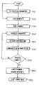
- FIG. 4is a process flow chart of a program which implements an embodiment of the atomic layer deposition method according to the present invention.
- workpieceincludes semiconductor substrate, printed circuits, and other structures that may be chemically treated by the method and system of the invention.
- substrateas used herein include any semiconductor-based or other structure having an exposed surface in which to form a structure using the system or method of this invention.
- Substrateis to be understood as including silicon-on-insulator, doped and undoped semiconductors, epitaxial layers of silicon supported by a base semiconductor foundation, and other semiconductor structures.
- previous process stepsmay have been utilized to form active devices, regions or junctions in the base semiconductor structure or foundation.
- FIG. 1discloses an improved atomic layer deposition method and apparatus according to the present invention providing a point of use generated/activated reactive gas species for processing a surface 2 of a workpiece 4 .
- a first precursor gas, indicated by 5is flown directly onto the surface 2 of the workpiece from a first gas port 6 a of a dispenser unit 8 .
- a flow of an input gas 10is provided from a second gas port 6 b in a direction away from the flow of the precursor gas 5 .
- the dispenser unit 8further includes a pair of evacuation ports 12 a and 12 b , and a third gas port 6 c .
- a pair of evacuation ports 12 a and 12 bjuxtaposed to the first evacuation port 12 a are the first and third gas ports, 6 a and 6 c
- a second evacuation port 12 bjuxtaposed to the second evacuation port 12 b are the second and third gas ports, 6 b and 6 c .
- the third gas port 6 cis used to flow a purge gas, indicated by 14 , directly onto the surface 2 of the workpiece.
- ALD pulse lengthsare determined by the space between the gas ports as well as a scan speed of workpiece. Accordingly, under properly adjusted processing conditions (i.e., deposition temperature, reactant dose, and length of precursor and purge gases pulses), scanning the workpiece 4 under the dispenser unit 8 in the direction indicated by “X”, leaves a chemisorbed monolayer of a surface reactant, illustrated by symbols “A”, on the surface 2 after the purge/pump sequence of the dispenser unit 8 with flows of the precursor gas 5 and purge gas 14 .
- processing conditionsi.e., deposition temperature, reactant dose, and length of precursor and purge gases pulses
- a beam of electromagnetic radiation 16is directed into the input gas 10 producing at the point of use a high flux of short-lived generated reactive gas species, illustrated by symbols “B”, by dissociating a gaseous constituent of the input gas 10 .
- the reactive gas species Breaches the surface 2 of the workpiece 4
- reactants A and Breact together in a complete and self-limiting reaction which forms a desired monolayer of a material, illustrated by symbol S, on the surface 2 of the workpiece 4 .
- Material monolayer Smay be an element or a compound. Therefore, the above-described multi-port dispenser unit 8 permits at the same time the formation of both surface reactant A on a first portion of the surface 2 of the workpiece 4 and the desired material monolayer S on a subsequent surface portion of the workpiece.
- the beam of electromagnetic radiation 16may advantageously be provided as a converging laser beam. Additionally, to ensure that maximum energy is provided at the focal point of the laser beam, a transmission gas 18 that is substantially nonattenuating to preselected wavelengths of electromagnetic radiation may be provided by a fourth gas port 6 d . Furthermore, the second gas port 6 b may be a nozzle providing a laminar flow of the input gas 10 over the surface 2 of the workpiece 4 such that the beam 16 converges in the flow in close proximity to the surface of the workpiece, but spaced a finite distance therefrom. This finite distant is indicated by symbol “H.” It is to be appreciated that the input gas is provided over the surface of the workpiece in a gas layer having a thickness that is at least large enough to accommodate the finite distance H.
- a laminar flowprevents the input gas from spiraling over the surface 2 of the workpiece 4 , thereby minimizing non-uniform distribution of the generated reactive gas species B.
- Bafflesmay be incorporated into the nozzle 6 b to break up the incoming gas stream into the desired laminar flow.
- the width of nozzle 6 bcan be made adjustable to optimize the gas flow rate for particular chemically treatments of the surface 2 of the workpiece 4 .
- distance Hthe beam 16 is focused in proximity to the surface 2 of the workpiece 4 such that maximum beam energy dissociates at the point of use a gaseous constituent of the input gas 10 into the high flux of generated reactive gas species B.
- distance His less than a few mean-free-path lengths of the generated reactive gas species B, or from about 2 millimeters to about 4 millimeters above the surface 2 of the workpiece 4 .
- the generated flux of reactive gas species Bis closes enough in order to migrate to the surface 2 , yet far enough that the focal point of the laser beam 16 does not inadvertently impact the workpiece 4 .
- the laser beam 16can dissociate more than one generated reactive gas species B depending on the composition of the input gas 10 , and also depending on the particular wavelength(s) of electromagnetic radiation present in the laser beam 16 . Therefore, besides reducing energy losses of the laser at its focal point, the present invention also gives access to new, quickly disappearing metastables that would otherwise disappear and never reach the surface 2 of the workpiece if formed well above the wafer surface.
- the above-described methodology and apparatusis further disclosed by the exemplary embodiments of a processing system 20 shown by FIGS. 2-4.
- FIG. 2is a diagrammatic sectional side view of the major component parts of an exemplary embodiment of a processing system 20 having a chamber 22 for containing the workpiece 4 to be processed.
- the workpiece 4comprises a semiconductor wafer of 1 to 8 inches in diameter and 0.127 to 0.89 mm thick, which is supported upon a conventional chuck 24 .
- the chamber 22is sealable such that it may contain and hold a subambient pressure of from about 0.1 Torr to about 100 Torr of a gaseous atmosphere, generally indicated by 26 , which is supplied to the chamber from first and second gas sources 28 a and 28 b , respectively.
- the first gas source 28 ais in gas communication with the chamber 22 , and provides the precursor and purge gases 5 and 14 , and optionally, transmission gas 18 .
- These gaseseach may be a single gas or a mixture of such gasses.
- the second gas source 28 bis also in gas communication with the chamber 22 and provides the input gas 10 .
- Gases 5 , 10 , 14 and/or 18are regulated in a conventional manner, such as for example, in-line pressure regulators 30 a and 30 b , values 32 a and 32 b , and mass flow meters 34 a and 34 b .
- in-line pressure regulators 30 a and 30 bvalues 32 a and 32 b
- mass flow meters 34 a and 34 bmass flow meters
- the gaseous atmosphere 26 within the chamber 22may be quickly evacuated by a first mechanical exhaust pump 38 a connected also in gas communication with the chamber via a first exhaust valve 40 a .
- first mechanical exhaust pump 38 aconnected also in gas communication with the chamber via a first exhaust valve 40 a .
- the entire gaseous atmosphere 26 within the chamber 22does not need to be purge or exhausted between pulse phases of the ALD process due to the purge/pump set-up of the dispenser unit 8 provided therein.
- the pair of evacuation ports 12 a and 12 b of the dispenser unitsare in gas communication with a second mechanical exhaust pump 38 b and regulated by a second exhaust valve 40 b for the above purpose.
- the input gas 10is a gas or mixture of gases that absorb predetermined wavelengths of electromagnetic energy and dissociate to form the desired generated reactive gas species B.
- gasesthat include: N 2 O, NO 2 , NH 3 , H 2 , H 2 O, N 2 , O 2 , O 3 , CCl 4 , BCl 3 , CDF 3 , CF 4 , SiH 4 , CFCl 3 , F 2 CO, (FCO) 2 , SF 5 NF 2 , N 2 F 4 , CF 3 Br, CF 3 NO, (CF 3 ) 2 CO, CF 2 HCl, CF 2 HBr, CF 2 Cl 2 , CF 2 Br 2 , CF 2 CFCl, CF 2 CFH, CF 2 CF 2 CH 2 , NH 3 , CHF 3 , fluorohalides, halocarbons, and combinations thereof.
- Such desired reactive gas species Binclude: NO, OH, NH, N, F, CF 3 , CF 2 , CF, NF 2 , NF, Cl, O, BCl 2 , BCl, FCO, and combinations thereof. It is to be appreciated that the choice of input gas 10 employed in a photoreactive treatment procedure is guided by the type of chemically treatment process to be carried out.
- the transmission gas 18is a gas or mixture of gases that is non-attenuating to predetermined wavelengths of electromagnetic radiation.
- Such transmission gasses, as well as the purge gasinclude argon, nitrogen, helium, neon, and combinations thereof.
- conditioning gasesmay be used such as to absorb electromagnetic radiation, to reduce the concentration of an reactive gas species, or as a catalyst for the reaction between the reactive gas species B and the reactant(s), such as surface reactant A.
- a conditioning gasmay be employed for controlling the reaction rate between the reactive gas species B and reactant A, or for creating a minimum reaction energy threshold for limiting the production of undesirable reaction products (e.g., ozone and hazardous polymer-based reaction products).
- conditioning gas moleculesinclude nitrogen, helium and argon.
- Nitrogenacts mainly to impede the reaction between material deficient regions and reactant gases, while argon tends to impede the diffusion of the primary reactant gas molecules, rather than to participate in a reaction.
- Heliumbehaves in an intermediate manner between nitrogen and argon.
- the chamber 22also contains a translation stage 42 to support the workpiece 4 in the chuck 24 and to move it in and out of the chamber 22 .
- the translation stage 42is electrically driven, and moves the chuck 24 and workpiece 4 held thereon back and forth within the chamber 22 at a constant rate (e.g., about 6.5 mm/sec) specified by a controller 44 .
- a constant ratee.g., about 6.5 mm/sec
- protruding banking pins 46spaced by about 120 degrees hold the workpiece 4 in place on the chuck 24 .
- the translation stage 42causes relative motion between the surface 2 of the workpiece 4 , the dispenser unit 8 , and the beam 16 such that the precursor gas 5 , purge gas 14 , and beam 16 sweeps or scans over the surface 2 of the substrate 4 during processing.
- the workpiece 4may be held stationary during processing, and the dispenser unit 8 and scanning optics 48 of a laser system 50 are moved to cause the desired relative motion between the surface 2 of the workpiece 4 , the dispenser unit 8 , and the beam 16 .
- the laser beam 16is shaped and delivered to the chamber 22 via the conventional laser system 50 that includes the scanning optics 48 , a laser controller 52 , and a laser source 54 .
- the scanning optics 48typically comprises one or more mirrors 56 (only one of which is shown) and focusing lenses 58 .
- the mirrors 56direct laser beam 16 towards the focusing lens 58 which shapes the conventional rectangular cross-section beam 16 received from the laser source 54 into a converging beam of electromagnetic energy proximate the surface 2 of the workpiece 4 .
- the focusing lens 58forms part of a window 60 of the chamber 22 , such as in the embodiment when relative motion is provided between the laser beam 16 and workpiece 4 by the translation stage 42 .
- the scanning optics 48 along with the focusing lens 58move relative to the window 60 to provide the desired scanning of the surface 2 of the workpiece 4 with beam 16 .
- the windows 60may be quartz, sapphire, or zinc selenide.
- the focusing lens 58is a cylindrical refractive lens, and both the lens 58 and window 60 are made from fused silica which allows visual inspection of the chamber 22 during a photoreactive treatment procedure, which is useful for monitoring the progress of a reaction as well as for end-point detection.
- laser beam 16is illustrated as a long narrow band 62 that extends across the major expanse of the surface 2 of the workpiece 4 during processing, it is to be understood that laser beam 16 can comprise other shapes.
- the beam 16may be provided as a circular beam which traverses across an entirety of the surface 2 of the workpiece 4 along the shown X and Y axes.
- the beam 16can be configured to be wide enough to cover an entirety of the surface 2 of the workpiece 4 without being passed across such surface.
- Laser source 54may be an excimer laser (for example, a Cymer CX-2 excimer laser available from Cymer Laser Technologies of San Diego, Calif., USA), which generates a pulsed beam 16 at wavelengths of 248 nm and 193 nm, and adapted to provide beam energy in the range of about 100 to about 5000 mJ/cm 2 .
- Other laserscould be used, e.g., a tunable Alexandrite solid state pulsed laser in combination with a frequency multiplier.
- the cross-sectional dimensions of the beam 16 from the laser source 54may be in the range of 3 mm ⁇ 5 mm to 5 mm ⁇ 15 mm.
- the scanning optics 48focuses beam 16 so that at distance H above the surface 2 of the workpiece 4 , the final beam gives the appearance of a knife-edge.
- the laser beam 16can predominantly comprise a single wavelength of ultraviolet light, and such wavelength can be chosen to interact with a specific constituent of the input gas 10 .
- a beam dump 63(FIG. 2) with a surface that strongly absorbs radiant energy in the range 157-250 nm (e.g., a block of hard-anodized aluminum with a row of narrow vanes oriented in the direction of the reflected laser beam) is mounted inside the chamber 22 .
- the beam dump 63receives radiant energy reflected from the surface 2 of the workpiece 4 during processing.
- a diagnostic laser beam 64 from a helium-neon laser 66may be introduced into the chamber 22 through the scanning optics 48 , and/or through the window 60 .
- a monitor 68could then be configured to receive a reflected diagnostic beam 64 to verify that the surface 2 has been treated without having to remove the workpiece 4 from the chamber 22 (e.g., by interferometric or light scattering techniques well-known in the field of surface analysis).
- the translation stage 42can comprise components for the temperature control of workpiece 4 during processing. Such components can include one or both of heating and cooling components 70 to maintain the workpiece 4 at a desired temperature. Additionally, the translation stage 42 may include various sensors that monitor pressure 72 , temperature 74 , and gases 76 in the chamber 22 .
- FIG. 2shows a block diagram of the controller 44 .
- the controller 44includes a programmable central processing unit (CPU) 202 that is operable with a memory 204 , a mass storage device 206 , an input control unit 208 , and a display unit 210 .
- CPUcentral processing unit
- FIG. 2shows a block diagram of the controller 44 .
- the controller 44includes a programmable central processing unit (CPU) 202 that is operable with a memory 204 , a mass storage device 206 , an input control unit 208 , and a display unit 210 .
- CPUcentral processing unit
- ASICapplication specific integrated circuit
- the controller 44further includes well-known support circuits 214 such as power supplies 216 , clocks 218 , cache 220 , input/output (I/O) circuits 222 and the like.
- the I/O circuitis connected to a control system bus 212 .
- the bus 212couples to the controller 44 the in-line flow regulators 30 a and 30 b , gas values 32 a and 32 b , mass flow meters 34 a and 34 b , exhaust pumps 38 a and 38 b , exhaust valves 40 a and 40 b , translation stage 42 , laser controller 52 , heating and cooling components 70 , chamber sensors 72 , 74 , and 76 , and a chamber door 78 .
- an electrically driven mechanical arm 80which moves the workpiece 4 in and out of the chamber 22 through the chamber door 78 to and from a transport device/chamber 82 , may be also controlled by the controller 44 .
- controller 44may include the following: mixing chambers 36 a and 36 b for mixing different gases, and if used, transition motors (not shown) for the dispenser unit 8 and scanning optics 48 . It is to be appreciated that the system controller 44 provides signals to the chamber elements to cause these elements to perform operations for forming the reactive gas species in the subject apparatus to accomplish atomic layer deposition, and other semi-conductor processing, if desired.
- the memory 204contains instructions that the CPU 202 executes to facilitate the performance of the processing system 20 .
- the instructions in the memory 204are in the form of program code such as a program 300 (FIG. 4) that implements the method of the present invention.
- the program codemay conform to any one of a number of different programming languages. For example, the program code can be written in C, C++, BASIC, Pascal, or a number of other languages.
- the mass storage device 206stores data and instructions and retrieves data and program code instructions from a processor-readable storage medium, such as a magnetic disk or magnetic tape.
- a processor-readable storage mediumsuch as a magnetic disk or magnetic tape.
- the mass storage device 206can be a hard disk drive, floppy disk drive, tape drive, or optical disk drive.
- the mass storage device 206stores and retrieves the instructions in response to directions that it receives from the CPU 202 .
- Data and program code instructions that are stored and retrieved by the mass storage device 206are employed by the processor unit 202 for operating the processing system 20 .
- the data and program code instructionsare first retrieved by the mass storage device 206 from a medium and then transferred to the memory 204 for use by the CPU 202 .
- the input control unit 208couples a data input device, such as a keyboard, mouse, or light pen, to the processor unit 202 to provide for the receipt of a chamber operator's inputs.
- the display unit 210provides information to a chamber operator in the form of graphical displays and alphanumeric characters under control of the CPU 202 .
- the control system bus 212provides for the transfer of data and control signals between all of the devices that are coupled to the control system bus 212 .
- the control system bus 212is displayed as a single bus that directly connects the devices in the CPU 202
- the control system bus 212can also be a collection of buses.
- the display unit 210 input control unit 208 and mass storage device 206can be coupled to an input-output peripheral bus, while the CPU 202 and memory 204 are coupled to a local processor bus.
- the local processor bus and input-output peripheral busare coupled to form the control system bus 212 .
- reaction parametersinclude, for example but are not limited to: energy wavelength, energy density of the incident laser beam, gas composition, pressure and mass flow rates of precursor gas 5 , input gas 10 , purge gas 14 , and optionally, transmission gas 12 inside the reaction chamber 22 , stage translation rate, and temperature of workpiece 4 .
- the workpiece 4 in step 320is loaded into the chamber 16 through door 78 , preferably from the transport device/chamber 82 , and positioned on the wafer chuck 24 against banking pins 46 , preferably by mechanical arm 80 , with the surface 2 to be treated facing up.
- the order of selecting reaction parameters in step 310 and loading in step 320is non-critical, and may be completed in any order or simultaneously.
- step 330mechanical pump 38 a pumps on the chamber 22 until a pressure of between about 1 and about 10 Torr is achieved.
- step 340the stage 42 translates the chuck 24 and workpiece 4 at a constant rate across the chamber 22 from a rear end 84 to a forward end 86 (FIG. 2 ).
- step 350the controller 44 electrically activates gas values 30 a and 30 b and flow regulators 32 a and 32 b (in proper sequence).
- the controller 44coordinates the delivery of precursor gas 5 , input gas 10 , and optionally transmission gas 12 (FIG. 1) from gas cylinders 28 a and 28 b through the dispenser unit 8 according to the selected reaction parameters.
- the controller 44coordinates the delivery of purge gas 14 , and the pumping on evacuation ports 12 a and 12 b by pump 38 b to prevent mixing of the precursor gas 5 and input gas 10 flows.
- step 360the controller 44 coordinates with the laser controller 52 to deliver the laser beam 16 into the input gas flow 10 .
- controller 44may be programmed to process the entire surface of the workpiece or a targeted portion. In either case, the controller 44 provides for the delivery of the laser beam 16 according to the selected reaction parameters such that the high flux of point of use reactive gas species B is generated at the proper time to react with surface reactant A at the selected locations of the surface 2 of the workpiece 4 . In most cases, the controller 44 will delay the generation of the high flux of point of use reactive gas species B until reactant A is translated into its proper position for such interaction with gas species B.
- step 370the controller 44 checks the formation of material monolayer S on the surface 2 of the workpiece 4 .
- the above deposition processesmay be repeated without removing the workpiece 4 from the reaction chamber 22 .
- the gas valves 20 a and 20 bare closed, the chamber 22 is purged in a conventional manner, and the workpiece 4 is then removed from the chamber 22 in step 380 to await a next workpiece 4 for processing in step 390 .
- the surface 2 of the workpiece 4may be desirous to chemically work the surface 2 of the workpiece 4 with only the generated reactive gas species B before or after such ALD processing.
- chemical treatmentsinclude, but not limited to, etching, cleaning, removing photoresist, and other applications which will be apparent to those of skill in the art given the teachings herein.
- the surface 2 of the workpiece 4may be treated as many times as required without being removed from the chamber 16 , and if desired, under different reaction conditions.
- the increase in production ratesresults from permitting the working of the surface 2 of the workpiece 4 with the high flux of a point of use generated reactive gas species while ahead of forming a surface reactant with a flow of a precursor gas without the need to completely purge or evacuate the entire reaction chamber.
- the present inventionmakes it possible to use two or more dispenser units to further increase the ALD process.
- another dispenser unitis provided, such as is illustrated by secondary dispenser unit 8 ′ and additionally radiation beam 16 ′ in FIG. 2 . Since the function of the secondary dispenser unit 8 ′ and beam 16 ′ are the same as dispenser unit 8 and beam 16 as described above, for brevity, no further discussion is provided as one skilled in the art would understand the use and benefit of such an arrangement.
Landscapes
- Chemical & Material Sciences (AREA)
- Engineering & Computer Science (AREA)
- General Chemical & Material Sciences (AREA)
- Chemical Kinetics & Catalysis (AREA)
- Materials Engineering (AREA)
- Mechanical Engineering (AREA)
- Metallurgy (AREA)
- Organic Chemistry (AREA)
- Physics & Mathematics (AREA)
- Fluid Mechanics (AREA)
- Electromagnetism (AREA)
- Plasma & Fusion (AREA)
- Optics & Photonics (AREA)
- Health & Medical Sciences (AREA)
- Toxicology (AREA)
- Chemical Vapour Deposition (AREA)
Abstract
Description
Claims (42)
Priority Applications (4)
| Application Number | Priority Date | Filing Date | Title |
|---|---|---|---|
| US10/091,938US6730367B2 (en) | 2002-03-05 | 2002-03-05 | Atomic layer deposition method with point of use generated reactive gas species |
| US10/697,511US7087119B2 (en) | 2002-03-05 | 2003-10-30 | Atomic layer deposition with point of use generated reactive gas species |
| US10/765,314US7455884B2 (en) | 2002-03-05 | 2004-01-27 | Atomic layer deposition with point of use generated reactive gas species |
| US11/450,657US20060225650A1 (en) | 2002-03-05 | 2006-06-09 | Atomic layer deposition apparatus with point of use generated reactive gas species |
Applications Claiming Priority (1)
| Application Number | Priority Date | Filing Date | Title |
|---|---|---|---|
| US10/091,938US6730367B2 (en) | 2002-03-05 | 2002-03-05 | Atomic layer deposition method with point of use generated reactive gas species |
Related Child Applications (2)
| Application Number | Title | Priority Date | Filing Date |
|---|---|---|---|
| US10/697,511DivisionUS7087119B2 (en) | 2002-03-05 | 2003-10-30 | Atomic layer deposition with point of use generated reactive gas species |
| US10/765,314DivisionUS7455884B2 (en) | 2002-03-05 | 2004-01-27 | Atomic layer deposition with point of use generated reactive gas species |
Publications (2)
| Publication Number | Publication Date |
|---|---|
| US20030170389A1 US20030170389A1 (en) | 2003-09-11 |
| US6730367B2true US6730367B2 (en) | 2004-05-04 |
Family
ID=27787768
Family Applications (4)
| Application Number | Title | Priority Date | Filing Date |
|---|---|---|---|
| US10/091,938Expired - LifetimeUS6730367B2 (en) | 2002-03-05 | 2002-03-05 | Atomic layer deposition method with point of use generated reactive gas species |
| US10/697,511Expired - LifetimeUS7087119B2 (en) | 2002-03-05 | 2003-10-30 | Atomic layer deposition with point of use generated reactive gas species |
| US10/765,314Expired - LifetimeUS7455884B2 (en) | 2002-03-05 | 2004-01-27 | Atomic layer deposition with point of use generated reactive gas species |
| US11/450,657AbandonedUS20060225650A1 (en) | 2002-03-05 | 2006-06-09 | Atomic layer deposition apparatus with point of use generated reactive gas species |
Family Applications After (3)
| Application Number | Title | Priority Date | Filing Date |
|---|---|---|---|
| US10/697,511Expired - LifetimeUS7087119B2 (en) | 2002-03-05 | 2003-10-30 | Atomic layer deposition with point of use generated reactive gas species |
| US10/765,314Expired - LifetimeUS7455884B2 (en) | 2002-03-05 | 2004-01-27 | Atomic layer deposition with point of use generated reactive gas species |
| US11/450,657AbandonedUS20060225650A1 (en) | 2002-03-05 | 2006-06-09 | Atomic layer deposition apparatus with point of use generated reactive gas species |
Country Status (1)
| Country | Link |
|---|---|
| US (4) | US6730367B2 (en) |
Cited By (34)
| Publication number | Priority date | Publication date | Assignee | Title |
|---|---|---|---|---|
| US20030170403A1 (en)* | 2002-03-11 | 2003-09-11 | Doan Trung Tri | Atomic layer deposition apparatus and method |
| US20030226500A1 (en)* | 2002-06-05 | 2003-12-11 | Derderian Garo J. | Atomic layer deposition apparatus and methods |
| US20040026374A1 (en)* | 2002-08-06 | 2004-02-12 | Tue Nguyen | Assembly line processing method |
| US20040065258A1 (en)* | 2002-10-08 | 2004-04-08 | Sandhu Gurtej S. | Atomic layer deposition methods and atomic layer deposition tools |
| US20040083951A1 (en)* | 2002-03-05 | 2004-05-06 | Sandhu Gurtej S. | Atomic layer deposition with point of use generated reactive gas species |
| US6793736B2 (en)* | 2001-11-30 | 2004-09-21 | Micron Technology, Inc. | Method of providing high flux of point of use activated reactive species for semiconductor processing |
| US20040224527A1 (en)* | 2002-08-15 | 2004-11-11 | Micron Technology, Inc. | Atomic layer deposition methods |
| US20040233010A1 (en)* | 2003-05-22 | 2004-11-25 | Salman Akram | Atomic layer deposition (ALD) high permeability layered magnetic films to reduce noise in high speed interconnection |
| US20050064212A1 (en)* | 2001-02-23 | 2005-03-24 | Dunlap Paul N. | Bonded part and method for producing same |
| US20050078462A1 (en)* | 2003-10-10 | 2005-04-14 | Micron Technology, Inc. | Laser assisted material deposition |
| US20060131702A1 (en)* | 1999-07-30 | 2006-06-22 | Micron Technology, Inc. | Novel transmission lines for CMOS integrated circuits |
| US20070077356A1 (en)* | 2005-09-20 | 2007-04-05 | Semiconductor Manufacturing International (Shanghai) Corporation | Method for atomic layer deposition of materials using an atmospheric pressure for semiconductor devices |
| US20080009140A1 (en)* | 2006-07-10 | 2008-01-10 | Micron Technology, Inc. | Electron induced chemical etching for device level diagnosis |
| US20080006603A1 (en)* | 2006-07-10 | 2008-01-10 | Micron Technology, Inc. | Electron induced chemical etching and deposition for local circuit repair |
| US20080038894A1 (en)* | 2006-08-14 | 2008-02-14 | Micron Technology, Inc. | Electronic beam processing device and method using carbon nanotube emitter |
| US20080105901A1 (en)* | 2006-11-07 | 2008-05-08 | Kamal Tabatabaie | Atomic layer deposition in the formation of gate structures for iii-v semiconductor |
| US7405454B2 (en) | 2003-03-04 | 2008-07-29 | Micron Technology, Inc. | Electronic apparatus with deposited dielectric layers |
| US20080299780A1 (en)* | 2007-06-01 | 2008-12-04 | Uv Tech Systems, Inc. | Method and apparatus for laser oxidation and reduction |
| US7498057B2 (en) | 2002-08-15 | 2009-03-03 | Micron Technology, Inc. | Deposition methods |
| US7560793B2 (en) | 2002-05-02 | 2009-07-14 | Micron Technology, Inc. | Atomic layer deposition and conversion |
| US7588988B2 (en) | 2004-08-31 | 2009-09-15 | Micron Technology, Inc. | Method of forming apparatus having oxide films formed using atomic layer deposition |
| US7670646B2 (en) | 2002-05-02 | 2010-03-02 | Micron Technology, Inc. | Methods for atomic-layer deposition |
| US20100166955A1 (en)* | 2008-11-01 | 2010-07-01 | Cambridge Nanotech Inc. | System and method for thin film deposition |
| US20100183825A1 (en)* | 2008-12-31 | 2010-07-22 | Cambridge Nanotech Inc. | Plasma atomic layer deposition system and method |
| US7791055B2 (en) | 2006-07-10 | 2010-09-07 | Micron Technology, Inc. | Electron induced chemical etching/deposition for enhanced detection of surface defects |
| US7791071B2 (en) | 2006-08-14 | 2010-09-07 | Micron Technology, Inc. | Profiling solid state samples |
| US20100247763A1 (en)* | 2008-11-01 | 2010-09-30 | Cambridge Nanotech Inc. | Reaction chamber with removable liner |
| US7833427B2 (en) | 2006-08-14 | 2010-11-16 | Micron Technology, Inc. | Electron beam etching device and method |
| US8501563B2 (en) | 2005-07-20 | 2013-08-06 | Micron Technology, Inc. | Devices with nanocrystals and methods of formation |
| WO2016186299A1 (en)* | 2015-05-15 | 2016-11-24 | 고려대학교 산학협력단 | Selective area atomic layer deposition apparatus |
| US9511663B2 (en) | 2013-05-29 | 2016-12-06 | Mcalister Technologies, Llc | Methods for fuel tank recycling and net hydrogen fuel and carbon goods production along with associated apparatus and systems |
| US9534296B2 (en) | 2013-03-15 | 2017-01-03 | Mcalister Technologies, Llc | Methods of manufacture of engineered materials and devices |
| TWI570263B (en)* | 2015-08-10 | 2017-02-11 | 炬力奈米科技有限公司 | Photo-assisted atomic layer deposition method |
| WO2019074553A1 (en) | 2017-10-12 | 2019-04-18 | Gelest Technologies, Inc. | Methods and system for the integrated synthesis, delivery, and processing of source chemicals for thin film manufacturing |
Families Citing this family (44)
| Publication number | Priority date | Publication date | Assignee | Title |
|---|---|---|---|---|
| US7258901B1 (en)* | 2000-09-08 | 2007-08-21 | Fei Company | Directed growth of nanotubes on a catalyst |
| US6852167B2 (en) | 2001-03-01 | 2005-02-08 | Micron Technology, Inc. | Methods, systems, and apparatus for uniform chemical-vapor depositions |
| US6953730B2 (en) | 2001-12-20 | 2005-10-11 | Micron Technology, Inc. | Low-temperature grown high quality ultra-thin CoTiO3 gate dielectrics |
| US7135421B2 (en) | 2002-06-05 | 2006-11-14 | Micron Technology, Inc. | Atomic layer-deposited hafnium aluminum oxide |
| US7221586B2 (en) | 2002-07-08 | 2007-05-22 | Micron Technology, Inc. | Memory utilizing oxide nanolaminates |
| US6921702B2 (en) | 2002-07-30 | 2005-07-26 | Micron Technology Inc. | Atomic layer deposited nanolaminates of HfO2/ZrO2 films as gate dielectrics |
| US7084078B2 (en) | 2002-08-29 | 2006-08-01 | Micron Technology, Inc. | Atomic layer deposited lanthanide doped TiOx dielectric films |
| US6958302B2 (en) | 2002-12-04 | 2005-10-25 | Micron Technology, Inc. | Atomic layer deposited Zr-Sn-Ti-O films using TiI4 |
| US7101813B2 (en) | 2002-12-04 | 2006-09-05 | Micron Technology Inc. | Atomic layer deposited Zr-Sn-Ti-O films |
| US7135369B2 (en) | 2003-03-31 | 2006-11-14 | Micron Technology, Inc. | Atomic layer deposited ZrAlxOy dielectric layers including Zr4AlO9 |
| US7192824B2 (en) | 2003-06-24 | 2007-03-20 | Micron Technology, Inc. | Lanthanide oxide / hafnium oxide dielectric layers |
| US7628860B2 (en)* | 2004-04-12 | 2009-12-08 | Mks Instruments, Inc. | Pulsed mass flow delivery system and method |
| US8133554B2 (en)* | 2004-05-06 | 2012-03-13 | Micron Technology, Inc. | Methods for depositing material onto microfeature workpieces in reaction chambers and systems for depositing materials onto microfeature workpieces |
| US7081421B2 (en) | 2004-08-26 | 2006-07-25 | Micron Technology, Inc. | Lanthanide oxide dielectric layer |
| US7494939B2 (en) | 2004-08-31 | 2009-02-24 | Micron Technology, Inc. | Methods for forming a lanthanum-metal oxide dielectric layer |
| US7235501B2 (en) | 2004-12-13 | 2007-06-26 | Micron Technology, Inc. | Lanthanum hafnium oxide dielectrics |
| US7828929B2 (en)* | 2004-12-30 | 2010-11-09 | Research Electro-Optics, Inc. | Methods and devices for monitoring and controlling thin film processing |
| US7374964B2 (en) | 2005-02-10 | 2008-05-20 | Micron Technology, Inc. | Atomic layer deposition of CeO2/Al2O3 films as gate dielectrics |
| US7687409B2 (en) | 2005-03-29 | 2010-03-30 | Micron Technology, Inc. | Atomic layer deposited titanium silicon oxide films |
| US7972441B2 (en)* | 2005-04-05 | 2011-07-05 | Applied Materials, Inc. | Thermal oxidation of silicon using ozone |
| FI119478B (en)* | 2005-04-22 | 2008-11-28 | Beneq Oy | Reactor |
| US7662729B2 (en) | 2005-04-28 | 2010-02-16 | Micron Technology, Inc. | Atomic layer deposition of a ruthenium layer to a lanthanide oxide dielectric layer |
| US7579285B2 (en)* | 2005-07-11 | 2009-08-25 | Imec | Atomic layer deposition method for depositing a layer |
| WO2008045130A2 (en)* | 2006-02-17 | 2008-04-17 | Cornell Research Foundation, Inc. | Property modification during film growth |
| US20070278180A1 (en)* | 2006-06-01 | 2007-12-06 | Williamson Mark J | Electron induced chemical etching for materials characterization |
| US7851377B2 (en)* | 2007-01-11 | 2010-12-14 | Taiwan Semiconductor Manufacturing Company, Ltd. | Chemical vapor deposition process |
| US8333839B2 (en)* | 2007-12-27 | 2012-12-18 | Synos Technology, Inc. | Vapor deposition reactor |
| JP4430718B2 (en)* | 2008-03-21 | 2010-03-10 | 三井造船株式会社 | Atomic layer deposition system |
| CN101621007A (en)* | 2008-07-03 | 2010-01-06 | 中芯国际集成电路制造(上海)有限公司 | SANOS memory cell structure |
| US20100037820A1 (en)* | 2008-08-13 | 2010-02-18 | Synos Technology, Inc. | Vapor Deposition Reactor |
| US8470718B2 (en)* | 2008-08-13 | 2013-06-25 | Synos Technology, Inc. | Vapor deposition reactor for forming thin film |
| US8147599B2 (en) | 2009-02-17 | 2012-04-03 | Mcalister Technologies, Llc | Apparatuses and methods for storing and/or filtering a substance |
| US8758512B2 (en)* | 2009-06-08 | 2014-06-24 | Veeco Ald Inc. | Vapor deposition reactor and method for forming thin film |
| US20110076421A1 (en)* | 2009-09-30 | 2011-03-31 | Synos Technology, Inc. | Vapor deposition reactor for forming thin film on curved surface |
| JP5050044B2 (en)* | 2009-12-14 | 2012-10-17 | 株式会社東芝 | Vapor growth method |
| FI124113B (en)* | 2010-08-30 | 2014-03-31 | Beneq Oy | Apparatus and method for working the surface of a substrate |
| US20120088370A1 (en)* | 2010-10-06 | 2012-04-12 | Lam Research Corporation | Substrate Processing System with Multiple Processing Devices Deployed in Shared Ambient Environment and Associated Methods |
| US8840958B2 (en) | 2011-02-14 | 2014-09-23 | Veeco Ald Inc. | Combined injection module for sequentially injecting source precursor and reactant precursor |
| WO2013025654A2 (en) | 2011-08-12 | 2013-02-21 | Mcalister Technologies, Llc | Fluid distribution filter having spiral filter media and associated systems and methods |
| FI124298B (en) | 2012-06-25 | 2014-06-13 | Beneq Oy | Apparatus for treating surface of substrate and nozzle head |
| KR102173047B1 (en)* | 2013-10-10 | 2020-11-03 | 삼성디스플레이 주식회사 | Vapor deposition apparatus |
| FR3032975B1 (en)* | 2015-02-23 | 2017-03-10 | Sidel Participations | PROCESS FOR PLASMA PROCESSING OF CONTAINERS COMPRISING A THERMAL IMAGING PHASE |
| US11377736B2 (en) | 2019-03-08 | 2022-07-05 | Seagate Technology Llc | Atomic layer deposition systems, methods, and devices |
| CN115702258B (en)* | 2020-06-10 | 2025-05-16 | 3M创新有限公司 | Roll-to-roll vapor deposition apparatus and method |
Citations (10)
| Publication number | Priority date | Publication date | Assignee | Title |
|---|---|---|---|---|
| US4260649A (en) | 1979-05-07 | 1981-04-07 | The Perkin-Elmer Corporation | Laser induced dissociative chemical gas phase processing of workpieces |
| US5270247A (en)* | 1991-07-12 | 1993-12-14 | Fujitsu Limited | Atomic layer epitaxy of compound semiconductor |
| US5607601A (en) | 1995-02-02 | 1997-03-04 | The Aerospace Corporation | Method for patterning and etching film layers of semiconductor devices |
| US5659383A (en) | 1995-11-17 | 1997-08-19 | Nikon Corporation | Exposure apparatus and exposure quantity control method |
| US5669979A (en) | 1993-09-08 | 1997-09-23 | Uvtech Systems, Inc. | Photoreactive surface processing |
| US5814156A (en) | 1993-09-08 | 1998-09-29 | Uvtech Systems Inc. | Photoreactive surface cleaning |
| US6448192B1 (en)* | 2001-04-16 | 2002-09-10 | Motorola, Inc. | Method for forming a high dielectric constant material |
| US6461909B1 (en)* | 2000-08-30 | 2002-10-08 | Micron Technology, Inc. | Process for fabricating RuSixOy-containing adhesion layers |
| US6503330B1 (en)* | 1999-12-22 | 2003-01-07 | Genus, Inc. | Apparatus and method to achieve continuous interface and ultrathin film during atomic layer deposition |
| US6509601B1 (en)* | 1998-07-31 | 2003-01-21 | Samsung Electronics Co., Ltd. | Semiconductor memory device having capacitor protection layer and method for manufacturing the same |
Family Cites Families (32)
| Publication number | Priority date | Publication date | Assignee | Title |
|---|---|---|---|---|
| US4176024A (en)* | 1975-07-28 | 1979-11-27 | Westinghouse Electric Corp. | Gas dynamic reaction process and system for laser chemistry |
| JPS59135730A (en)* | 1983-01-24 | 1984-08-04 | Hitachi Ltd | surface modification equipment |
| JPH0766906B2 (en)* | 1984-07-26 | 1995-07-19 | 新技術事業団 | GaAs epitaxial growth method |
| GB2162207B (en)* | 1984-07-26 | 1989-05-10 | Japan Res Dev Corp | Semiconductor crystal growth apparatus |
| US4924807A (en)* | 1986-07-26 | 1990-05-15 | Nihon Shinku Gijutsu Kabushiki Kaisha | Apparatus for chemical vapor deposition |
| US4774416A (en)* | 1986-09-24 | 1988-09-27 | Plaser Corporation | Large cross-sectional area molecular beam source for semiconductor processing |
| US4734152A (en)* | 1986-12-22 | 1988-03-29 | Massachusetts Institute Of Technology | Dry etching patterning of electrical and optical materials |
| IL84255A (en)* | 1987-10-23 | 1993-02-21 | Galram Technology Ind Ltd | Process for removal of post- baked photoresist layer |
| US5023424A (en) | 1990-01-22 | 1991-06-11 | Tencor Instruments | Shock wave particle removal method and apparatus |
| US5290383A (en)* | 1991-03-24 | 1994-03-01 | Tokyo Electron Limited | Plasma-process system with improved end-point detecting scheme |
| US5174826A (en)* | 1991-12-06 | 1992-12-29 | General Electric Company | Laser-assisted chemical vapor deposition |
| US5330610A (en)* | 1993-05-28 | 1994-07-19 | Martin Marietta Energy Systems, Inc. | Method of digital epilaxy by externally controlled closed-loop feedback |
| US6200389B1 (en)* | 1994-07-18 | 2001-03-13 | Silicon Valley Group Thermal Systems Llc | Single body injector and deposition chamber |
| EP0704551B1 (en)* | 1994-09-27 | 2000-09-06 | Applied Materials, Inc. | Method of processing a substrate in a vacuum processing chamber |
| US5637188A (en)* | 1995-02-17 | 1997-06-10 | Colorado Seminary | Processing substrates with a photon-enhanced neutral beam |
| US5509601A (en)* | 1995-08-28 | 1996-04-23 | Drabick; Ronald | Internal package spacer/protector |
| US5772771A (en)* | 1995-12-13 | 1998-06-30 | Applied Materials, Inc. | Deposition chamber for improved deposition thickness uniformity |
| US6070551A (en)* | 1996-05-13 | 2000-06-06 | Applied Materials, Inc. | Deposition chamber and method for depositing low dielectric constant films |
| US5972430A (en)* | 1997-11-26 | 1999-10-26 | Advanced Technology Materials, Inc. | Digital chemical vapor deposition (CVD) method for forming a multi-component oxide layer |
| US6203865B1 (en)* | 1998-07-20 | 2001-03-20 | Qqc, Inc. | Laser approaches for diamond synthesis |
| US6190732B1 (en)* | 1998-09-03 | 2001-02-20 | Cvc Products, Inc. | Method and system for dispensing process gas for fabricating a device on a substrate |
| US6136719A (en)* | 1999-04-30 | 2000-10-24 | Lsi Logic Corporation | Method and arrangement for fabricating a semiconductor device |
| JP3664033B2 (en)* | 2000-03-29 | 2005-06-22 | セイコーエプソン株式会社 | Ceramic manufacturing method and manufacturing apparatus thereof |
| KR100458982B1 (en)* | 2000-08-09 | 2004-12-03 | 주성엔지니어링(주) | Semiconductor device fabrication apparatus having rotatable gas injector and thin film deposition method using the same |
| JP3709134B2 (en) | 2000-11-22 | 2005-10-19 | 松下電器産業株式会社 | Square battery |
| US6573199B2 (en)* | 2001-08-30 | 2003-06-03 | Micron Technology, Inc. | Methods of treating dielectric materials with oxygen, and methods of forming capacitor constructions |
| US6461436B1 (en)* | 2001-10-15 | 2002-10-08 | Micron Technology, Inc. | Apparatus and process of improving atomic layer deposition chamber performance |
| US7001481B2 (en)* | 2001-11-30 | 2006-02-21 | Micron Technology, Inc. | Method and system providing high flux of point of use activated reactive species for semiconductor processing |
| US6730367B2 (en)* | 2002-03-05 | 2004-05-04 | Micron Technology, Inc. | Atomic layer deposition method with point of use generated reactive gas species |
| US20040129212A1 (en)* | 2002-05-20 | 2004-07-08 | Gadgil Pradad N. | Apparatus and method for delivery of reactive chemical precursors to the surface to be treated |
| US20040058293A1 (en)* | 2002-08-06 | 2004-03-25 | Tue Nguyen | Assembly line processing system |
| US6821563B2 (en)* | 2002-10-02 | 2004-11-23 | Applied Materials, Inc. | Gas distribution system for cyclical layer deposition |
- 2002
- 2002-03-05USUS10/091,938patent/US6730367B2/ennot_activeExpired - Lifetime
- 2003
- 2003-10-30USUS10/697,511patent/US7087119B2/ennot_activeExpired - Lifetime
- 2004
- 2004-01-27USUS10/765,314patent/US7455884B2/ennot_activeExpired - Lifetime
- 2006
- 2006-06-09USUS11/450,657patent/US20060225650A1/ennot_activeAbandoned
Patent Citations (10)
| Publication number | Priority date | Publication date | Assignee | Title |
|---|---|---|---|---|
| US4260649A (en) | 1979-05-07 | 1981-04-07 | The Perkin-Elmer Corporation | Laser induced dissociative chemical gas phase processing of workpieces |
| US5270247A (en)* | 1991-07-12 | 1993-12-14 | Fujitsu Limited | Atomic layer epitaxy of compound semiconductor |
| US5669979A (en) | 1993-09-08 | 1997-09-23 | Uvtech Systems, Inc. | Photoreactive surface processing |
| US5814156A (en) | 1993-09-08 | 1998-09-29 | Uvtech Systems Inc. | Photoreactive surface cleaning |
| US5607601A (en) | 1995-02-02 | 1997-03-04 | The Aerospace Corporation | Method for patterning and etching film layers of semiconductor devices |
| US5659383A (en) | 1995-11-17 | 1997-08-19 | Nikon Corporation | Exposure apparatus and exposure quantity control method |
| US6509601B1 (en)* | 1998-07-31 | 2003-01-21 | Samsung Electronics Co., Ltd. | Semiconductor memory device having capacitor protection layer and method for manufacturing the same |
| US6503330B1 (en)* | 1999-12-22 | 2003-01-07 | Genus, Inc. | Apparatus and method to achieve continuous interface and ultrathin film during atomic layer deposition |
| US6461909B1 (en)* | 2000-08-30 | 2002-10-08 | Micron Technology, Inc. | Process for fabricating RuSixOy-containing adhesion layers |
| US6448192B1 (en)* | 2001-04-16 | 2002-09-10 | Motorola, Inc. | Method for forming a high dielectric constant material |
Non-Patent Citations (1)
| Title |
|---|
| Prasad, Vinay; Gobbert, Matthias K.; Cale, Timothy S.; Prediction of Deposition Rates in Atomic Layer Deposition No citation, dates, pages provided. |
Cited By (83)
| Publication number | Priority date | Publication date | Assignee | Title |
|---|---|---|---|---|
| US20060131702A1 (en)* | 1999-07-30 | 2006-06-22 | Micron Technology, Inc. | Novel transmission lines for CMOS integrated circuits |
| US7869242B2 (en) | 1999-07-30 | 2011-01-11 | Micron Technology, Inc. | Transmission lines for CMOS integrated circuits |
| US7554829B2 (en) | 1999-07-30 | 2009-06-30 | Micron Technology, Inc. | Transmission lines for CMOS integrated circuits |
| US20050064212A1 (en)* | 2001-02-23 | 2005-03-24 | Dunlap Paul N. | Bonded part and method for producing same |
| US6793736B2 (en)* | 2001-11-30 | 2004-09-21 | Micron Technology, Inc. | Method of providing high flux of point of use activated reactive species for semiconductor processing |
| US7087119B2 (en)* | 2002-03-05 | 2006-08-08 | Micron Technology, Inc. | Atomic layer deposition with point of use generated reactive gas species |
| US20040083951A1 (en)* | 2002-03-05 | 2004-05-06 | Sandhu Gurtej S. | Atomic layer deposition with point of use generated reactive gas species |
| US7455884B2 (en) | 2002-03-05 | 2008-11-25 | Micron Technology, Inc. | Atomic layer deposition with point of use generated reactive gas species |
| US20040185184A1 (en)* | 2002-03-05 | 2004-09-23 | Sandhu Gurtej S. | Atomic layer deposition with point of use generated reactive gas species |
| US20060225650A1 (en)* | 2002-03-05 | 2006-10-12 | Sandhu Gurtej S | Atomic layer deposition apparatus with point of use generated reactive gas species |
| US6893506B2 (en) | 2002-03-11 | 2005-05-17 | Micron Technology, Inc. | Atomic layer deposition apparatus and method |
| US7431773B2 (en) | 2002-03-11 | 2008-10-07 | Micron Technology, Inc. | Atomic layer deposition apparatus and method |
| US20060144333A1 (en)* | 2002-03-11 | 2006-07-06 | Doan Trung T | Atomic layer deposition apparatus and method |
| US7030037B2 (en) | 2002-03-11 | 2006-04-18 | Micron Technology, Inc. | Atomic layer deposition apparatus and method |
| US20050142890A1 (en)* | 2002-03-11 | 2005-06-30 | Doan Trung T. | Atomic layer deposition apparatus and method |
| US20030170403A1 (en)* | 2002-03-11 | 2003-09-11 | Doan Trung Tri | Atomic layer deposition apparatus and method |
| US20040129219A1 (en)* | 2002-03-11 | 2004-07-08 | Doan Trung Tri | Atomic layer deposition apparatus and method |
| US7560793B2 (en) | 2002-05-02 | 2009-07-14 | Micron Technology, Inc. | Atomic layer deposition and conversion |
| US7670646B2 (en) | 2002-05-02 | 2010-03-02 | Micron Technology, Inc. | Methods for atomic-layer deposition |
| US7589029B2 (en) | 2002-05-02 | 2009-09-15 | Micron Technology, Inc. | Atomic layer deposition and conversion |
| US6896730B2 (en) | 2002-06-05 | 2005-05-24 | Micron Technology, Inc. | Atomic layer deposition apparatus and methods |
| US20030226500A1 (en)* | 2002-06-05 | 2003-12-11 | Derderian Garo J. | Atomic layer deposition apparatus and methods |
| US20040026374A1 (en)* | 2002-08-06 | 2004-02-12 | Tue Nguyen | Assembly line processing method |
| US7153542B2 (en)* | 2002-08-06 | 2006-12-26 | Tegal Corporation | Assembly line processing method |
| US20080241386A1 (en)* | 2002-08-15 | 2008-10-02 | Micron Technology, Inc. | Atomic Layer Deposition Methods |
| US7303991B2 (en)* | 2002-08-15 | 2007-12-04 | Micron Technology, Inc. | Atomic layer deposition methods |
| US20060205227A1 (en)* | 2002-08-15 | 2006-09-14 | Demetrius Sarigiannis | Atomic layer deposition methods |
| US20040224527A1 (en)* | 2002-08-15 | 2004-11-11 | Micron Technology, Inc. | Atomic layer deposition methods |
| US7498057B2 (en) | 2002-08-15 | 2009-03-03 | Micron Technology, Inc. | Deposition methods |
| US20060205228A1 (en)* | 2002-08-15 | 2006-09-14 | Demetrius Sarigiannis | Atomic layer deposition methods |
| US7378354B2 (en)* | 2002-08-15 | 2008-05-27 | Micron Technology, Inc. | Atomic layer deposition methods |
| US7368382B2 (en)* | 2002-08-15 | 2008-05-06 | Micron Technology, Inc. | Atomic layer deposition methods |
| US7279041B2 (en) | 2002-10-08 | 2007-10-09 | Micron Technology, Inc. | Atomic layer deposition methods and atomic layer deposition tools |
| US20040065258A1 (en)* | 2002-10-08 | 2004-04-08 | Sandhu Gurtej S. | Atomic layer deposition methods and atomic layer deposition tools |
| US6916374B2 (en) | 2002-10-08 | 2005-07-12 | Micron Technology, Inc. | Atomic layer deposition methods and atomic layer deposition tools |
| US20050245093A1 (en)* | 2002-10-08 | 2005-11-03 | Sandhu Gurtej S | Atomic layer deposition methods and atomic layer deposition tools |
| US7405454B2 (en) | 2003-03-04 | 2008-07-29 | Micron Technology, Inc. | Electronic apparatus with deposited dielectric layers |
| US6970053B2 (en) | 2003-05-22 | 2005-11-29 | Micron Technology, Inc. | Atomic layer deposition (ALD) high permeability layered magnetic films to reduce noise in high speed interconnection |
| US20050140462A1 (en)* | 2003-05-22 | 2005-06-30 | Micron Technology, Inc. | High permeability layered magnetic films to reduce noise in high speed interconnection |
| US7154354B2 (en) | 2003-05-22 | 2006-12-26 | Micron Technology, Inc. | High permeability layered magnetic films to reduce noise in high speed interconnection |
| US20040233010A1 (en)* | 2003-05-22 | 2004-11-25 | Salman Akram | Atomic layer deposition (ALD) high permeability layered magnetic films to reduce noise in high speed interconnection |
| US20060289969A1 (en)* | 2003-10-10 | 2006-12-28 | Micron Technology, Inc. | Laser assisted material deposition |
| US20060288937A1 (en)* | 2003-10-10 | 2006-12-28 | Micron Technology, Inc. | Laser assisted material deposition |
| US7311947B2 (en) | 2003-10-10 | 2007-12-25 | Micron Technology, Inc. | Laser assisted material deposition |
| US20050078462A1 (en)* | 2003-10-10 | 2005-04-14 | Micron Technology, Inc. | Laser assisted material deposition |
| US8541276B2 (en) | 2004-08-31 | 2013-09-24 | Micron Technology, Inc. | Methods of forming an insulating metal oxide |
| US8154066B2 (en) | 2004-08-31 | 2012-04-10 | Micron Technology, Inc. | Titanium aluminum oxide films |
| US7588988B2 (en) | 2004-08-31 | 2009-09-15 | Micron Technology, Inc. | Method of forming apparatus having oxide films formed using atomic layer deposition |
| US8921914B2 (en) | 2005-07-20 | 2014-12-30 | Micron Technology, Inc. | Devices with nanocrystals and methods of formation |
| US8501563B2 (en) | 2005-07-20 | 2013-08-06 | Micron Technology, Inc. | Devices with nanocrystals and methods of formation |
| US20070077356A1 (en)* | 2005-09-20 | 2007-04-05 | Semiconductor Manufacturing International (Shanghai) Corporation | Method for atomic layer deposition of materials using an atmospheric pressure for semiconductor devices |
| US7887884B2 (en)* | 2005-09-20 | 2011-02-15 | Semiconductor Manufacturing International (Shanghai) Corporation | Method for atomic layer deposition of materials using an atmospheric pressure for semiconductor devices |
| US8026501B2 (en) | 2006-07-10 | 2011-09-27 | Micron Technology, Inc. | Method of removing or deposting material on a surface including material selected to decorate a particle on the surface for imaging |
| US7892978B2 (en) | 2006-07-10 | 2011-02-22 | Micron Technology, Inc. | Electron induced chemical etching for device level diagnosis |
| US20080009140A1 (en)* | 2006-07-10 | 2008-01-10 | Micron Technology, Inc. | Electron induced chemical etching for device level diagnosis |
| US7791055B2 (en) | 2006-07-10 | 2010-09-07 | Micron Technology, Inc. | Electron induced chemical etching/deposition for enhanced detection of surface defects |
| US8821682B2 (en) | 2006-07-10 | 2014-09-02 | Micron Technology, Inc. | Electron induced chemical etching and deposition for local circuit repair |
| US8809074B2 (en) | 2006-07-10 | 2014-08-19 | Micron Technology, Inc. | Method for integrated circuit diagnosis |
| US7807062B2 (en) | 2006-07-10 | 2010-10-05 | Micron Technology, Inc. | Electron induced chemical etching and deposition for local circuit repair |
| US20080006603A1 (en)* | 2006-07-10 | 2008-01-10 | Micron Technology, Inc. | Electron induced chemical etching and deposition for local circuit repair |
| US20110139368A1 (en)* | 2006-07-10 | 2011-06-16 | Williamson Mark J | Apparatus and systems for integrated circuit diagnosis |
| US20110017401A1 (en)* | 2006-07-10 | 2011-01-27 | Williamson Mark J | Electron induced chemical etching and deposition for local circuit repair |
| US7718080B2 (en) | 2006-08-14 | 2010-05-18 | Micron Technology, Inc. | Electronic beam processing device and method using carbon nanotube emitter |
| US20110056625A1 (en)* | 2006-08-14 | 2011-03-10 | Rueger Neal R | Electron beam etching device and method |
| US7791071B2 (en) | 2006-08-14 | 2010-09-07 | Micron Technology, Inc. | Profiling solid state samples |
| US8389415B2 (en) | 2006-08-14 | 2013-03-05 | Micron Technology, Inc. | Profiling solid state samples |
| US8414787B2 (en) | 2006-08-14 | 2013-04-09 | Micron Technology, Inc. | Electron beam processing device and method using carbon nanotube emitter |
| US20080038894A1 (en)* | 2006-08-14 | 2008-02-14 | Micron Technology, Inc. | Electronic beam processing device and method using carbon nanotube emitter |
| US7833427B2 (en) | 2006-08-14 | 2010-11-16 | Micron Technology, Inc. | Electron beam etching device and method |
| US8609542B2 (en) | 2006-08-14 | 2013-12-17 | Micron Technology, Inc. | Profiling solid state samples |
| US7692222B2 (en) | 2006-11-07 | 2010-04-06 | Raytheon Company | Atomic layer deposition in the formation of gate structures for III-V semiconductor |
| US20080105901A1 (en)* | 2006-11-07 | 2008-05-08 | Kamal Tabatabaie | Atomic layer deposition in the formation of gate structures for iii-v semiconductor |
| US20080299780A1 (en)* | 2007-06-01 | 2008-12-04 | Uv Tech Systems, Inc. | Method and apparatus for laser oxidation and reduction |
| US20100247763A1 (en)* | 2008-11-01 | 2010-09-30 | Cambridge Nanotech Inc. | Reaction chamber with removable liner |
| US20100166955A1 (en)* | 2008-11-01 | 2010-07-01 | Cambridge Nanotech Inc. | System and method for thin film deposition |
| US9175388B2 (en) | 2008-11-01 | 2015-11-03 | Ultratech, Inc. | Reaction chamber with removable liner |
| US9328417B2 (en) | 2008-11-01 | 2016-05-03 | Ultratech, Inc. | System and method for thin film deposition |
| US20100183825A1 (en)* | 2008-12-31 | 2010-07-22 | Cambridge Nanotech Inc. | Plasma atomic layer deposition system and method |
| US9534296B2 (en) | 2013-03-15 | 2017-01-03 | Mcalister Technologies, Llc | Methods of manufacture of engineered materials and devices |
| US9511663B2 (en) | 2013-05-29 | 2016-12-06 | Mcalister Technologies, Llc | Methods for fuel tank recycling and net hydrogen fuel and carbon goods production along with associated apparatus and systems |
| WO2016186299A1 (en)* | 2015-05-15 | 2016-11-24 | 고려대학교 산학협력단 | Selective area atomic layer deposition apparatus |
| TWI570263B (en)* | 2015-08-10 | 2017-02-11 | 炬力奈米科技有限公司 | Photo-assisted atomic layer deposition method |
| WO2019074553A1 (en) | 2017-10-12 | 2019-04-18 | Gelest Technologies, Inc. | Methods and system for the integrated synthesis, delivery, and processing of source chemicals for thin film manufacturing |
Also Published As
| Publication number | Publication date |
|---|---|
| US20060225650A1 (en) | 2006-10-12 |
| US20040083951A1 (en) | 2004-05-06 |
| US20030170389A1 (en) | 2003-09-11 |
| US7087119B2 (en) | 2006-08-08 |
| US7455884B2 (en) | 2008-11-25 |
| US20040185184A1 (en) | 2004-09-23 |
Similar Documents
| Publication | Publication Date | Title |
|---|---|---|
| US6730367B2 (en) | Atomic layer deposition method with point of use generated reactive gas species | |
| US6793736B2 (en) | Method of providing high flux of point of use activated reactive species for semiconductor processing | |
| US5344522A (en) | Pattern forming process and process for preparing semiconductor device utilizing said pattern forming process | |
| US8986562B2 (en) | Methods of laser processing photoresist in a gaseous environment | |
| US4716852A (en) | Apparatus for thin film formation using photo-induced chemical reaction | |
| JP2019519918A (en) | Atomic layer etching system and method | |
| US6350391B1 (en) | Laser stripping improvement by modified gas composition | |
| US4260649A (en) | Laser induced dissociative chemical gas phase processing of workpieces | |
| US4643799A (en) | Method of dry etching | |
| US6178973B1 (en) | Method and apparatus for ozone generation and surface treatment | |
| US20050175789A1 (en) | Method for energy-assisted atomic layer deposition and removal | |
| US20070196011A1 (en) | Integrated vacuum metrology for cluster tool | |
| WO2019217180A1 (en) | Atomic layer etch and deposition processing systems including a lens circuit with a tele-centric lens, an optical beam folding assembly, or a polygon scanner | |
| JPS6175529A (en) | Dry etching method and device | |
| JP2009044169A (en) | Methods and apparatus for processing semiconductor wafer using plasma processing chamber in wafer track environment | |
| US20080296258A1 (en) | Plenum reactor system | |
| US7270724B2 (en) | Scanning plasma reactor | |
| KR100544226B1 (en) | Method and apparatus for radical oxidation of silicon | |
| JP3258121B2 (en) | CVD equipment | |
| JP2667930B2 (en) | Fine processing method and device | |
| JPS60124816A (en) | Thin film growth method | |
| JPS6196725A (en) | Photo chemical vapor deposition method |
Legal Events
| Date | Code | Title | Description |
|---|---|---|---|
| AS | Assignment | Owner name:MICRON TECHNOLOGY, INC., IDAHO Free format text:ASSIGNMENT OF ASSIGNORS INTEREST;ASSIGNOR:SANDHU, GURTEJ S.;REEL/FRAME:012864/0255 Effective date:20020221 | |
| STCF | Information on status: patent grant | Free format text:PATENTED CASE | |
| CC | Certificate of correction | ||
| FPAY | Fee payment | Year of fee payment:4 | |
| FPAY | Fee payment | Year of fee payment:8 | |
| FPAY | Fee payment | Year of fee payment:12 | |
| AS | Assignment | Owner name:U.S. BANK NATIONAL ASSOCIATION, AS COLLATERAL AGENT, CALIFORNIA Free format text:SECURITY INTEREST;ASSIGNOR:MICRON TECHNOLOGY, INC.;REEL/FRAME:038669/0001 Effective date:20160426 Owner name:U.S. BANK NATIONAL ASSOCIATION, AS COLLATERAL AGEN Free format text:SECURITY INTEREST;ASSIGNOR:MICRON TECHNOLOGY, INC.;REEL/FRAME:038669/0001 Effective date:20160426 | |
| AS | Assignment | Owner name:MORGAN STANLEY SENIOR FUNDING, INC., AS COLLATERAL AGENT, MARYLAND Free format text:PATENT SECURITY AGREEMENT;ASSIGNOR:MICRON TECHNOLOGY, INC.;REEL/FRAME:038954/0001 Effective date:20160426 Owner name:MORGAN STANLEY SENIOR FUNDING, INC., AS COLLATERAL Free format text:PATENT SECURITY AGREEMENT;ASSIGNOR:MICRON TECHNOLOGY, INC.;REEL/FRAME:038954/0001 Effective date:20160426 | |
| AS | Assignment | Owner name:U.S. BANK NATIONAL ASSOCIATION, AS COLLATERAL AGENT, CALIFORNIA Free format text:CORRECTIVE ASSIGNMENT TO CORRECT THE REPLACE ERRONEOUSLY FILED PATENT #7358718 WITH THE CORRECT PATENT #7358178 PREVIOUSLY RECORDED ON REEL 038669 FRAME 0001. ASSIGNOR(S) HEREBY CONFIRMS THE SECURITY INTEREST;ASSIGNOR:MICRON TECHNOLOGY, INC.;REEL/FRAME:043079/0001 Effective date:20160426 Owner name:U.S. BANK NATIONAL ASSOCIATION, AS COLLATERAL AGEN Free format text:CORRECTIVE ASSIGNMENT TO CORRECT THE REPLACE ERRONEOUSLY FILED PATENT #7358718 WITH THE CORRECT PATENT #7358178 PREVIOUSLY RECORDED ON REEL 038669 FRAME 0001. ASSIGNOR(S) HEREBY CONFIRMS THE SECURITY INTEREST;ASSIGNOR:MICRON TECHNOLOGY, INC.;REEL/FRAME:043079/0001 Effective date:20160426 | |
| AS | Assignment | Owner name:JPMORGAN CHASE BANK, N.A., AS COLLATERAL AGENT, ILLINOIS Free format text:SECURITY INTEREST;ASSIGNORS:MICRON TECHNOLOGY, INC.;MICRON SEMICONDUCTOR PRODUCTS, INC.;REEL/FRAME:047540/0001 Effective date:20180703 Owner name:JPMORGAN CHASE BANK, N.A., AS COLLATERAL AGENT, IL Free format text:SECURITY INTEREST;ASSIGNORS:MICRON TECHNOLOGY, INC.;MICRON SEMICONDUCTOR PRODUCTS, INC.;REEL/FRAME:047540/0001 Effective date:20180703 | |
| AS | Assignment | Owner name:MICRON TECHNOLOGY, INC., IDAHO Free format text:RELEASE BY SECURED PARTY;ASSIGNOR:U.S. BANK NATIONAL ASSOCIATION, AS COLLATERAL AGENT;REEL/FRAME:047243/0001 Effective date:20180629 | |
| AS | Assignment | Owner name:MICRON TECHNOLOGY, INC., IDAHO Free format text:RELEASE BY SECURED PARTY;ASSIGNOR:MORGAN STANLEY SENIOR FUNDING, INC., AS COLLATERAL AGENT;REEL/FRAME:050937/0001 Effective date:20190731 | |
| AS | Assignment | Owner name:MICRON SEMICONDUCTOR PRODUCTS, INC., IDAHO Free format text:RELEASE BY SECURED PARTY;ASSIGNOR:JPMORGAN CHASE BANK, N.A., AS COLLATERAL AGENT;REEL/FRAME:051028/0001 Effective date:20190731 Owner name:MICRON TECHNOLOGY, INC., IDAHO Free format text:RELEASE BY SECURED PARTY;ASSIGNOR:JPMORGAN CHASE BANK, N.A., AS COLLATERAL AGENT;REEL/FRAME:051028/0001 Effective date:20190731 |