US6728913B1 - Data recycling in memory - Google Patents
Data recycling in memoryDownload PDFInfo
- Publication number
- US6728913B1 US6728913B1US09/513,698US51369800AUS6728913B1US 6728913 B1US6728913 B1US 6728913B1US 51369800 AUS51369800 AUS 51369800AUS 6728913 B1US6728913 B1US 6728913B1
- Authority
- US
- United States
- Prior art keywords
- memory
- page
- data
- errors
- memory cells
- Prior art date
- Legal status (The legal status is an assumption and is not a legal conclusion. Google has not performed a legal analysis and makes no representation as to the accuracy of the status listed.)
- Expired - Lifetime
Links
Images


Classifications
- G—PHYSICS
- G06—COMPUTING OR CALCULATING; COUNTING
- G06F—ELECTRIC DIGITAL DATA PROCESSING
- G06F11/00—Error detection; Error correction; Monitoring
- G06F11/004—Error avoidance
- G—PHYSICS
- G11—INFORMATION STORAGE
- G11C—STATIC STORES
- G11C16/00—Erasable programmable read-only memories
- G11C16/02—Erasable programmable read-only memories electrically programmable
- G11C16/06—Auxiliary circuits, e.g. for writing into memory
- G11C16/34—Determination of programming status, e.g. threshold voltage, overprogramming or underprogramming, retention
- G11C16/3418—Disturbance prevention or evaluation; Refreshing of disturbed memory data
- G11C16/3431—Circuits or methods to detect disturbed nonvolatile memory cells, e.g. which still read as programmed but with threshold less than the program verify threshold or read as erased but with threshold greater than the erase verify threshold, and to reverse the disturbance via a refreshing programming or erasing step
Definitions
- a flash cellcan be a field effect transistor (FET) including a select gate, a floating gate, a drain, and a source.
- FETfield effect transistor
- a cellcan be read by grounding the source, and applying a voltage to a bitline connected with the drain. By applying a voltage to the wordline connected to select gate, the cell can be switched on and off.
- Flash memory cellscan be grouped into NAND type and NOR type circuits.
- NAND flash memory cellshave an n cell transistors connected in series and are connected in parallel between bit lines and ground lines.
- NAND flash memory cellsare useful in large scale integration.
- NOR flash memory cellsinclude cell transistors that are connected in parallel between bit lines and ground lines. NOR flash memory cells provide high-speed operation.
- Programming a cellincludes trapping excess electrons in the floating gate to increase voltage. This reduces the current conducted by the memory cell when the select voltage is applied to the select gate.
- the memory cellis programmed when the cell current is less than a reference current and the select voltage is applied.
- the cellis erased when the cell current is greater than the reference current and the select voltage is applied.
- Existing memory refresh circuitsrefresh data on a cell by cell basis or a time basis, such as hourly. Refreshing the data takes time and may not be necessary every hour, day, etc.
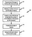
- a method of programming a memory device having a plurality of pages of memoryincludes programming the memory, monitoring the memory for defects, creating a copy of the data, erasing the old version of the data, and rewriting the data.
- the first page of memoryis programmed with a first data set.
- the first page of memoryis monitored for errors. During the monitoring for errors, some detected errors may be corrected. When the number of errors detected exceeds a threshold, a copy of that page of is created.
- the number of errors detectedcan be a fixed number a percentage of the memory, or time dependent.
- the copycan be created in an other page of local memory of in remote memory. Then the first page of memory is erased. Finally, the first data set rewritten.
- FIG. 1is a circuit diagram of the selects for the page erase mechanism.
- FIG. 2is a circuit diagram of the page erase mechanism.
- FIG. 3is an illustration of an embodiment of a memory.
- FIG. 4is a flow diagram of a method of programming a memory with a plurality of memory pages.
- FIG. 1shows a diagram of the selects for the page erase mechanism 100 .
- the page erase mechanism 100includes a two selects “Select 1 ” 102 and “Select 2 ” 110 . These selects select which page of memory is being erased.
- the page erase lines 104 , 106 , and 108each are connected to a separate page of memory for example page 15 , 14 , and 0 respectively.
- the page erase mechanism 100can control more pages of memory than shown for example, 10 pages, 100 pages, or 1 million pages or more.
- the voltage applied to the page erase lines 104 , 106 , and 108indicates which page of memory, if any, are being erased.
- the page of memorywill be erased when the page erase line associated with it is has zero volts (0V) applied to it.
- the pages of memory not being erasedcan have 10V applied to them.
- the Vss applied to the bitlinecan be for example 20 volts.
- FIG. 2shows a circuit diagram of the page erase mechanism 200 .
- the page erase mechanism 200includes a Bit Sel 204 , a QVER latch 208 an erase verify control 206 , a QDAT latch 212 , and a read/program control 210 .
- the output of the page erase mechanism 200is sent to the input/output bus (I/O bus) 214 .
- I/O businput/output bus
- Bit Sel 204enables the bit line.
- the erase verify control 206verifies the erase occurred.
- the QVER latch 208performs erase, read, and program verify.
- the QVER latch 208completes the operation the data is no longer in the QVER latch 208 .
- the QDAT latch 208stores the data and puts the data on the I/O bus 214 ond back to the bi line depending on which operation is being performed.
- QDATis bit data storage used in the program or read operations.
- the read/program circuit 210controls whether data is being read from the memory or whether data is being programmed(written) to the memory.
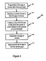
- a method of programming a memory device with a plurality of pages of memoryincludes programming, monitoring, creating a copy, erasing, and recycling.
- the first page of memoryis programmed with a first data set. More than one page of memory can be programmed.
- a page of memorycan be a group of memory cells, a sector of memory cells, a single cell or a plurality of memory cells such as 4096 cells.
- the memory cellscan be non-volatile memory including non-volatile NAND flash memory.
- the first page of memoryis monitored for errors. During monitoring for errors, some detected errors can be corrected.
- the error correctioncan include using error correction code.
- the errorscan occur for “read disturb” or “data retention” or other sources.
- the QDAT latch 208When a number of errors are detected, a copy of that page of memory is created in the QDAT latch 208 .
- the number of errors detectedcan be a fixed number such as 1 to 100,000; it can be a percentage of the memory cells, such as 0.1% to 50%; or it can be a time dependent threshold such as an error rate per second.
- the first page of memoryis erased using the QVER latch 208 .
- the first data set recyclingincludes rewriting, restoring, or reprogramming the data in its original location. Each page of memory can be separately monitored, erase, and recycled.
- the QDAT Latch 208is used to restore the corrected data.
- a recyclable programmable memory deviceincludes a memory array, a programming circuit, an error detection circuit, an erase circuit, and a recycling circuit.
- the memory arrayhas at least one page of memory cells and preferably a plurality of pages of memory.
- the programming circuitis capable of storing data in the memory cells.
- the error detection circuitis capable of detecting errors in the data stored in the memory cells and optionally includes an error correction circuit.
- the erase circuitis capable of erasing the memory cells on a page by page basis.
- the erase circuitcan erase the page of memory after a number of errors are detected by the error detection circuit.
- the number of errorscan be a fixed number or a percentage of the memory cells in the page.
- the recycling circuitis capable of restoring the data in the memory cells after the erase circuit has erased those cells. When multiple the memory array includes multiple pages of memory, each page of memory can be monitored, erased, and recycled independently.
- the term “circuit”includes hardware only, combined hardware and software, and software only and is not meant to be limited
- FIG. 3is an illustration of an embodiment of a memory 300 with memory cells 302 , a detection circuit 304 with optional error correction circuit, an erase circuit 308 , and a programming circuit 310 .
- FIG. 4is a flow diagram of a method of programming memory 400 with a plurality of memory pages.
- a first page of memory with a first data setis programmed.
- a number of errors in the first page of memoryare detected.
- a copy of the first data set when the number of errors detected in 404 exceeds an error thresholdis created.
- the first page of memoryis erased.
- the first data set in the first memory pageis stored.
Landscapes
- Engineering & Computer Science (AREA)
- Theoretical Computer Science (AREA)
- Quality & Reliability (AREA)
- Physics & Mathematics (AREA)
- General Engineering & Computer Science (AREA)
- General Physics & Mathematics (AREA)
- Read Only Memory (AREA)
- For Increasing The Reliability Of Semiconductor Memories (AREA)
Abstract
Description
Claims (20)
Priority Applications (1)
| Application Number | Priority Date | Filing Date | Title |
|---|---|---|---|
| US09/513,698US6728913B1 (en) | 2000-02-25 | 2000-02-25 | Data recycling in memory |
Applications Claiming Priority (1)
| Application Number | Priority Date | Filing Date | Title |
|---|---|---|---|
| US09/513,698US6728913B1 (en) | 2000-02-25 | 2000-02-25 | Data recycling in memory |
Publications (1)
| Publication Number | Publication Date |
|---|---|
| US6728913B1true US6728913B1 (en) | 2004-04-27 |
Family
ID=32108315
Family Applications (1)
| Application Number | Title | Priority Date | Filing Date |
|---|---|---|---|
| US09/513,698Expired - LifetimeUS6728913B1 (en) | 2000-02-25 | 2000-02-25 | Data recycling in memory |
Country Status (1)
| Country | Link |
|---|---|
| US (1) | US6728913B1 (en) |
Cited By (47)
| Publication number | Priority date | Publication date | Assignee | Title |
|---|---|---|---|---|
| US20040202034A1 (en)* | 2003-04-03 | 2004-10-14 | Jin-Yub Lee | Nonvolatile memory with error correction for page copy operation and method thereof |
| US20070174642A1 (en)* | 2006-01-25 | 2007-07-26 | Cornwell Michael J | Reporting flash memory operating voltages |
| US20070174641A1 (en)* | 2006-01-25 | 2007-07-26 | Cornwell Michael J | Adjusting power supplies for data storage devices |
| US20070180328A1 (en)* | 2006-01-27 | 2007-08-02 | Cornwell Michael J | Monitoring health of non-volatile memory |
| US20080080241A1 (en)* | 2006-08-15 | 2008-04-03 | Chunchun Ho | Method for recycling flash memory |
| US20080303350A1 (en)* | 2007-06-07 | 2008-12-11 | Samsung Electronics Co., Ltd. | High voltage power supply |
| US20090254777A1 (en)* | 2005-12-13 | 2009-10-08 | Gemplus | Detector of Abnormal Destruction of Memory Sectors |
| WO2010043245A1 (en)* | 2008-10-13 | 2010-04-22 | Hyperstone Gmbh | Method for backing up an anchor block in flash memories |
| US20100199134A1 (en)* | 2009-02-03 | 2010-08-05 | Micron Technology, Inc. | Determining sector status in a memory device |
| US20110035540A1 (en)* | 2009-08-10 | 2011-02-10 | Adtron, Inc. | Flash blade system architecture and method |
| US7913032B1 (en) | 2007-04-25 | 2011-03-22 | Apple Inc. | Initiating memory wear leveling |
| EP2245542A4 (en)* | 2008-02-29 | 2011-04-13 | Toshiba Kk | Semiconductor storage device |
| WO2013143578A1 (en)* | 2012-03-27 | 2013-10-03 | Alstom Technology Ltd | Non-volatile memory assemblies |
| US8745328B2 (en) | 2007-04-25 | 2014-06-03 | Apple Inc. | Updating error correction codes for data blocks |
| US8909851B2 (en) | 2011-02-08 | 2014-12-09 | SMART Storage Systems, Inc. | Storage control system with change logging mechanism and method of operation thereof |
| US8935466B2 (en) | 2011-03-28 | 2015-01-13 | SMART Storage Systems, Inc. | Data storage system with non-volatile memory and method of operation thereof |
| US8949689B2 (en) | 2012-06-11 | 2015-02-03 | SMART Storage Systems, Inc. | Storage control system with data management mechanism and method of operation thereof |
| US8983823B1 (en) | 2005-12-29 | 2015-03-17 | The Mathworks, Inc. | Verification harness for automatically generating a text-based representation of a graphical model |
| US9021319B2 (en) | 2011-09-02 | 2015-04-28 | SMART Storage Systems, Inc. | Non-volatile memory management system with load leveling and method of operation thereof |
| US9021231B2 (en) | 2011-09-02 | 2015-04-28 | SMART Storage Systems, Inc. | Storage control system with write amplification control mechanism and method of operation thereof |
| US9043780B2 (en) | 2013-03-27 | 2015-05-26 | SMART Storage Systems, Inc. | Electronic system with system modification control mechanism and method of operation thereof |
| US9063844B2 (en) | 2011-09-02 | 2015-06-23 | SMART Storage Systems, Inc. | Non-volatile memory management system with time measure mechanism and method of operation thereof |
| US9098399B2 (en) | 2011-08-31 | 2015-08-04 | SMART Storage Systems, Inc. | Electronic system with storage management mechanism and method of operation thereof |
| US9123445B2 (en) | 2013-01-22 | 2015-09-01 | SMART Storage Systems, Inc. | Storage control system with data management mechanism and method of operation thereof |
| US9146850B2 (en) | 2013-08-01 | 2015-09-29 | SMART Storage Systems, Inc. | Data storage system with dynamic read threshold mechanism and method of operation thereof |
| US9152555B2 (en) | 2013-11-15 | 2015-10-06 | Sandisk Enterprise IP LLC. | Data management with modular erase in a data storage system |
| US9170941B2 (en) | 2013-04-05 | 2015-10-27 | Sandisk Enterprises IP LLC | Data hardening in a storage system |
| US9183137B2 (en) | 2013-02-27 | 2015-11-10 | SMART Storage Systems, Inc. | Storage control system with data management mechanism and method of operation thereof |
| US9214965B2 (en) | 2013-02-20 | 2015-12-15 | Sandisk Enterprise Ip Llc | Method and system for improving data integrity in non-volatile storage |
| US9239781B2 (en) | 2012-02-07 | 2016-01-19 | SMART Storage Systems, Inc. | Storage control system with erase block mechanism and method of operation thereof |
| US9244519B1 (en) | 2013-06-25 | 2016-01-26 | Smart Storage Systems. Inc. | Storage system with data transfer rate adjustment for power throttling |
| US9292631B1 (en) | 2005-12-29 | 2016-03-22 | The Mathworks, Inc. | Automatic comparison and performance analysis between different implementations |
| US9298252B2 (en) | 2012-04-17 | 2016-03-29 | SMART Storage Systems, Inc. | Storage control system with power down mechanism and method of operation thereof |
| US9313874B2 (en) | 2013-06-19 | 2016-04-12 | SMART Storage Systems, Inc. | Electronic system with heat extraction and method of manufacture thereof |
| US9329928B2 (en) | 2013-02-20 | 2016-05-03 | Sandisk Enterprise IP LLC. | Bandwidth optimization in a non-volatile memory system |
| US9361222B2 (en) | 2013-08-07 | 2016-06-07 | SMART Storage Systems, Inc. | Electronic system with storage drive life estimation mechanism and method of operation thereof |
| US9367353B1 (en) | 2013-06-25 | 2016-06-14 | Sandisk Technologies Inc. | Storage control system with power throttling mechanism and method of operation thereof |
| US9431113B2 (en) | 2013-08-07 | 2016-08-30 | Sandisk Technologies Llc | Data storage system with dynamic erase block grouping mechanism and method of operation thereof |
| US9448946B2 (en) | 2013-08-07 | 2016-09-20 | Sandisk Technologies Llc | Data storage system with stale data mechanism and method of operation thereof |
| US9470720B2 (en) | 2013-03-08 | 2016-10-18 | Sandisk Technologies Llc | Test system with localized heating and method of manufacture thereof |
| CN106201346A (en)* | 2016-06-30 | 2016-12-07 | 联想(北京)有限公司 | A kind of data processing method and storage device |
| US9543025B2 (en) | 2013-04-11 | 2017-01-10 | Sandisk Technologies Llc | Storage control system with power-off time estimation mechanism and method of operation thereof |
| US9671962B2 (en) | 2012-11-30 | 2017-06-06 | Sandisk Technologies Llc | Storage control system with data management mechanism of parity and method of operation thereof |
| US9898056B2 (en) | 2013-06-19 | 2018-02-20 | Sandisk Technologies Llc | Electronic assembly with thermal channel and method of manufacture thereof |
| US10049037B2 (en) | 2013-04-05 | 2018-08-14 | Sandisk Enterprise Ip Llc | Data management in a storage system |
| US10546648B2 (en) | 2013-04-12 | 2020-01-28 | Sandisk Technologies Llc | Storage control system with data management mechanism and method of operation thereof |
| US11249845B2 (en) | 2017-12-06 | 2022-02-15 | Rambus Inc. | Error-correction-detection coding for hybrid memory module |
Citations (11)
| Publication number | Priority date | Publication date | Assignee | Title |
|---|---|---|---|---|
| US4493081A (en) | 1981-06-26 | 1985-01-08 | Computer Automation, Inc. | Dynamic memory with error correction on refresh |
| US4612640A (en) | 1984-02-21 | 1986-09-16 | Seeq Technology, Inc. | Error checking and correction circuitry for use with an electrically-programmable and electrically-erasable memory array |
| US4958350A (en) | 1988-03-02 | 1990-09-18 | Stardent Computer, Inc. | Error detecting/correction code and apparatus |
| US5450424A (en) | 1992-07-27 | 1995-09-12 | Mitsubishi Denki Kabushiki Kaisha | Semiconductor memory device with error checking and correcting function |
| US5532962A (en)* | 1992-05-20 | 1996-07-02 | Sandisk Corporation | Soft errors handling in EEPROM devices |
| US5546402A (en)* | 1992-09-11 | 1996-08-13 | International Business Machines Corporation | Flash-erase-type nonvolatile semiconductor storage device |
| US5606532A (en)* | 1995-03-17 | 1997-02-25 | Atmel Corporation | EEPROM array with flash-like core |
| US5956352A (en) | 1992-04-24 | 1999-09-21 | Digital Equipment Corporation | Adjustable filter for error detecting and correcting system |
| US6002612A (en)* | 1995-12-04 | 1999-12-14 | Sony Corporation | Nonvolatile semiconductor memory with fast data programming and erasing function using ECC |
| US6058046A (en)* | 1994-09-30 | 2000-05-02 | Kabushiki Kaisha Toshiba | Nonvolatile semiconductor memory cell capable of saving overwritten cell and its saving method |
| US6058047A (en) | 1996-08-16 | 2000-05-02 | Tokyo Electron Limited | Semiconductor memory device having error detection and correction |
- 2000
- 2000-02-25USUS09/513,698patent/US6728913B1/ennot_activeExpired - Lifetime
Patent Citations (11)
| Publication number | Priority date | Publication date | Assignee | Title |
|---|---|---|---|---|
| US4493081A (en) | 1981-06-26 | 1985-01-08 | Computer Automation, Inc. | Dynamic memory with error correction on refresh |
| US4612640A (en) | 1984-02-21 | 1986-09-16 | Seeq Technology, Inc. | Error checking and correction circuitry for use with an electrically-programmable and electrically-erasable memory array |
| US4958350A (en) | 1988-03-02 | 1990-09-18 | Stardent Computer, Inc. | Error detecting/correction code and apparatus |
| US5956352A (en) | 1992-04-24 | 1999-09-21 | Digital Equipment Corporation | Adjustable filter for error detecting and correcting system |
| US5532962A (en)* | 1992-05-20 | 1996-07-02 | Sandisk Corporation | Soft errors handling in EEPROM devices |
| US5450424A (en) | 1992-07-27 | 1995-09-12 | Mitsubishi Denki Kabushiki Kaisha | Semiconductor memory device with error checking and correcting function |
| US5546402A (en)* | 1992-09-11 | 1996-08-13 | International Business Machines Corporation | Flash-erase-type nonvolatile semiconductor storage device |
| US6058046A (en)* | 1994-09-30 | 2000-05-02 | Kabushiki Kaisha Toshiba | Nonvolatile semiconductor memory cell capable of saving overwritten cell and its saving method |
| US5606532A (en)* | 1995-03-17 | 1997-02-25 | Atmel Corporation | EEPROM array with flash-like core |
| US6002612A (en)* | 1995-12-04 | 1999-12-14 | Sony Corporation | Nonvolatile semiconductor memory with fast data programming and erasing function using ECC |
| US6058047A (en) | 1996-08-16 | 2000-05-02 | Tokyo Electron Limited | Semiconductor memory device having error detection and correction |
Non-Patent Citations (1)
| Title |
|---|
| Choi et al., A High Speed Programming Scheme for Multi-Level NAND Flash Memory, 1996, IEEE< P. 170-171.* |
Cited By (72)
| Publication number | Priority date | Publication date | Assignee | Title |
|---|---|---|---|---|
| US7296128B2 (en)* | 2003-04-03 | 2007-11-13 | Samsung Electronics Co., Ltd. | Nonvolatile memory with error correction for page copy operation and method thereof |
| US20040202034A1 (en)* | 2003-04-03 | 2004-10-14 | Jin-Yub Lee | Nonvolatile memory with error correction for page copy operation and method thereof |
| US20080163030A1 (en)* | 2003-04-03 | 2008-07-03 | Samsung Electronics Co., Ltd. | Nonvolatile memory with error correction for page copy operation and method thereof |
| US7934133B2 (en)* | 2005-12-13 | 2011-04-26 | Gemalto Sa | Detector of abnormal destruction of memory sectors |
| US20090254777A1 (en)* | 2005-12-13 | 2009-10-08 | Gemplus | Detector of Abnormal Destruction of Memory Sectors |
| US9880922B1 (en) | 2005-12-29 | 2018-01-30 | The Mathworks, Inc. | System and method for automatically generating a graphical model from a text-based program |
| US8983823B1 (en) | 2005-12-29 | 2015-03-17 | The Mathworks, Inc. | Verification harness for automatically generating a text-based representation of a graphical model |
| US9292631B1 (en) | 2005-12-29 | 2016-03-22 | The Mathworks, Inc. | Automatic comparison and performance analysis between different implementations |
| US9317629B1 (en) | 2005-12-29 | 2016-04-19 | The Mathworks, Inc. | Automatic comparison and performance analysis between different implementations |
| US9317628B1 (en)* | 2005-12-29 | 2016-04-19 | The Mathworks, Inc. | Automatic comparison and performance analysis between different implementations |
| US7702935B2 (en) | 2006-01-25 | 2010-04-20 | Apple Inc. | Reporting flash memory operating voltages |
| US20100162012A1 (en)* | 2006-01-25 | 2010-06-24 | Apple Inc. | Reporting flash memory operating voltages |
| US20070174641A1 (en)* | 2006-01-25 | 2007-07-26 | Cornwell Michael J | Adjusting power supplies for data storage devices |
| US8171318B2 (en) | 2006-01-25 | 2012-05-01 | Apple Inc. | Reporting flash memory operating voltages |
| US20070174642A1 (en)* | 2006-01-25 | 2007-07-26 | Cornwell Michael J | Reporting flash memory operating voltages |
| US7861122B2 (en)* | 2006-01-27 | 2010-12-28 | Apple Inc. | Monitoring health of non-volatile memory |
| US20070180328A1 (en)* | 2006-01-27 | 2007-08-02 | Cornwell Michael J | Monitoring health of non-volatile memory |
| US7478271B2 (en)* | 2006-08-15 | 2009-01-13 | Chunchun Ho | Method for recycling flash memory |
| US20080080241A1 (en)* | 2006-08-15 | 2008-04-03 | Chunchun Ho | Method for recycling flash memory |
| US8677057B1 (en) | 2007-04-25 | 2014-03-18 | Apple Inc. | Initiating memory wear leveling |
| US7913032B1 (en) | 2007-04-25 | 2011-03-22 | Apple Inc. | Initiating memory wear leveling |
| US8745328B2 (en) | 2007-04-25 | 2014-06-03 | Apple Inc. | Updating error correction codes for data blocks |
| US20080303350A1 (en)* | 2007-06-07 | 2008-12-11 | Samsung Electronics Co., Ltd. | High voltage power supply |
| EP2245542A4 (en)* | 2008-02-29 | 2011-04-13 | Toshiba Kk | Semiconductor storage device |
| US8219861B2 (en) | 2008-02-29 | 2012-07-10 | Kabushiki Kaisha Toshiba | Semiconductor storage device |
| US8583972B2 (en)* | 2008-02-29 | 2013-11-12 | Kabushiki Kaisha Toshiba | Method of controlling a semiconductor storage device |
| US9037947B2 (en)* | 2008-02-29 | 2015-05-19 | Kabushiki Kaisha Toshiba | Method of controlling a semiconductor storage device |
| US20120239992A1 (en)* | 2008-02-29 | 2012-09-20 | Kabushiki Kaisha Toshiba | Method of controlling a semiconductor storage device |
| US8793555B2 (en)* | 2008-02-29 | 2014-07-29 | Kabushiki Kaisha Toshiba | Method of controlling a semiconductor storage device |
| US20140304567A1 (en)* | 2008-02-29 | 2014-10-09 | Kabushiki Kaisha Toshiba | Method of controlling a semiconductor storage device |
| US8060797B2 (en) | 2008-02-29 | 2011-11-15 | Kabushiki Kaisha Toshiba | Semiconductor storage device |
| TWI397916B (en)* | 2008-02-29 | 2013-06-01 | Toshiba Kk | Semiconductor storage device |
| WO2010043245A1 (en)* | 2008-10-13 | 2010-04-22 | Hyperstone Gmbh | Method for backing up an anchor block in flash memories |
| US8276042B2 (en)* | 2009-02-03 | 2012-09-25 | Micron Technology, Inc. | Determining sector status in a memory device |
| US20100199134A1 (en)* | 2009-02-03 | 2010-08-05 | Micron Technology, Inc. | Determining sector status in a memory device |
| US9165653B2 (en) | 2009-02-03 | 2015-10-20 | Micron Technology, Inc. | Determining sector status in a memory device |
| US20110035540A1 (en)* | 2009-08-10 | 2011-02-10 | Adtron, Inc. | Flash blade system architecture and method |
| US8909851B2 (en) | 2011-02-08 | 2014-12-09 | SMART Storage Systems, Inc. | Storage control system with change logging mechanism and method of operation thereof |
| US8935466B2 (en) | 2011-03-28 | 2015-01-13 | SMART Storage Systems, Inc. | Data storage system with non-volatile memory and method of operation thereof |
| US9098399B2 (en) | 2011-08-31 | 2015-08-04 | SMART Storage Systems, Inc. | Electronic system with storage management mechanism and method of operation thereof |
| US9063844B2 (en) | 2011-09-02 | 2015-06-23 | SMART Storage Systems, Inc. | Non-volatile memory management system with time measure mechanism and method of operation thereof |
| US9021231B2 (en) | 2011-09-02 | 2015-04-28 | SMART Storage Systems, Inc. | Storage control system with write amplification control mechanism and method of operation thereof |
| US9021319B2 (en) | 2011-09-02 | 2015-04-28 | SMART Storage Systems, Inc. | Non-volatile memory management system with load leveling and method of operation thereof |
| US9239781B2 (en) | 2012-02-07 | 2016-01-19 | SMART Storage Systems, Inc. | Storage control system with erase block mechanism and method of operation thereof |
| WO2013143578A1 (en)* | 2012-03-27 | 2013-10-03 | Alstom Technology Ltd | Non-volatile memory assemblies |
| US9298252B2 (en) | 2012-04-17 | 2016-03-29 | SMART Storage Systems, Inc. | Storage control system with power down mechanism and method of operation thereof |
| US8949689B2 (en) | 2012-06-11 | 2015-02-03 | SMART Storage Systems, Inc. | Storage control system with data management mechanism and method of operation thereof |
| US9671962B2 (en) | 2012-11-30 | 2017-06-06 | Sandisk Technologies Llc | Storage control system with data management mechanism of parity and method of operation thereof |
| US9123445B2 (en) | 2013-01-22 | 2015-09-01 | SMART Storage Systems, Inc. | Storage control system with data management mechanism and method of operation thereof |
| US9214965B2 (en) | 2013-02-20 | 2015-12-15 | Sandisk Enterprise Ip Llc | Method and system for improving data integrity in non-volatile storage |
| US9329928B2 (en) | 2013-02-20 | 2016-05-03 | Sandisk Enterprise IP LLC. | Bandwidth optimization in a non-volatile memory system |
| US9183137B2 (en) | 2013-02-27 | 2015-11-10 | SMART Storage Systems, Inc. | Storage control system with data management mechanism and method of operation thereof |
| US9470720B2 (en) | 2013-03-08 | 2016-10-18 | Sandisk Technologies Llc | Test system with localized heating and method of manufacture thereof |
| US9043780B2 (en) | 2013-03-27 | 2015-05-26 | SMART Storage Systems, Inc. | Electronic system with system modification control mechanism and method of operation thereof |
| US10049037B2 (en) | 2013-04-05 | 2018-08-14 | Sandisk Enterprise Ip Llc | Data management in a storage system |
| US9170941B2 (en) | 2013-04-05 | 2015-10-27 | Sandisk Enterprises IP LLC | Data hardening in a storage system |
| US9543025B2 (en) | 2013-04-11 | 2017-01-10 | Sandisk Technologies Llc | Storage control system with power-off time estimation mechanism and method of operation thereof |
| US10546648B2 (en) | 2013-04-12 | 2020-01-28 | Sandisk Technologies Llc | Storage control system with data management mechanism and method of operation thereof |
| US9313874B2 (en) | 2013-06-19 | 2016-04-12 | SMART Storage Systems, Inc. | Electronic system with heat extraction and method of manufacture thereof |
| US9898056B2 (en) | 2013-06-19 | 2018-02-20 | Sandisk Technologies Llc | Electronic assembly with thermal channel and method of manufacture thereof |
| US9367353B1 (en) | 2013-06-25 | 2016-06-14 | Sandisk Technologies Inc. | Storage control system with power throttling mechanism and method of operation thereof |
| US9244519B1 (en) | 2013-06-25 | 2016-01-26 | Smart Storage Systems. Inc. | Storage system with data transfer rate adjustment for power throttling |
| US9146850B2 (en) | 2013-08-01 | 2015-09-29 | SMART Storage Systems, Inc. | Data storage system with dynamic read threshold mechanism and method of operation thereof |
| US9361222B2 (en) | 2013-08-07 | 2016-06-07 | SMART Storage Systems, Inc. | Electronic system with storage drive life estimation mechanism and method of operation thereof |
| US9448946B2 (en) | 2013-08-07 | 2016-09-20 | Sandisk Technologies Llc | Data storage system with stale data mechanism and method of operation thereof |
| US9431113B2 (en) | 2013-08-07 | 2016-08-30 | Sandisk Technologies Llc | Data storage system with dynamic erase block grouping mechanism and method of operation thereof |
| US9665295B2 (en) | 2013-08-07 | 2017-05-30 | Sandisk Technologies Llc | Data storage system with dynamic erase block grouping mechanism and method of operation thereof |
| US9152555B2 (en) | 2013-11-15 | 2015-10-06 | Sandisk Enterprise IP LLC. | Data management with modular erase in a data storage system |
| CN106201346B (en)* | 2016-06-30 | 2019-06-25 | 联想(北京)有限公司 | A kind of data processing method and storage equipment |
| CN106201346A (en)* | 2016-06-30 | 2016-12-07 | 联想(北京)有限公司 | A kind of data processing method and storage device |
| US11249845B2 (en) | 2017-12-06 | 2022-02-15 | Rambus Inc. | Error-correction-detection coding for hybrid memory module |
| US11782788B2 (en) | 2017-12-06 | 2023-10-10 | Rambus Inc. | Error-correction-detection coding for hybrid memory module |
Similar Documents
| Publication | Publication Date | Title |
|---|---|---|
| US6728913B1 (en) | Data recycling in memory | |
| US8730737B2 (en) | Method and system for minimizing number of programming pulses used to program rows of non-volatile memory cells | |
| US8432743B2 (en) | Method and system for programming non-volatile memory cells based on programming of proximate memory cells | |
| US6049899A (en) | Soft errors handling in EEPROM devices | |
| US5532962A (en) | Soft errors handling in EEPROM devices | |
| US8074122B2 (en) | Program failure recovery | |
| US7800953B2 (en) | Method and system for selectively limiting peak power consumption during programming or erase of non-volatile memory devices | |
| US7457155B2 (en) | Non-volatile memory device and method having bit-state assignments selected to minimize signal coupling | |
| JP3076195B2 (en) | Nonvolatile semiconductor memory device | |
| KR100953063B1 (en) | Erasing Method of Nonvolatile Memory Device | |
| JP2004514238A (en) | Page erasable flash memory and control method thereof | |
| US9520184B2 (en) | Method for writing in-system programming code into flash memory for better noise margin | |
| KR960005370B1 (en) | Method and apparatus for erasing and verifying nonvolatile semiconductor memory devices | |
| US6128224A (en) | Method and apparatus for writing an erasable non-volatile memory | |
| KR100871700B1 (en) | Error Data Correction Method Due to Charge Loss in Nonvolatile Memory Devices | |
| US20140355357A1 (en) | Method for writing in an eeprom-type memory including a memory cell refresh | |
| CN105321566A (en) | Semiconductor memory device and programming method thereof | |
| JP5731622B2 (en) | Flash memory, bad block management method and management program | |
| TWI530957B (en) | Flash memory, management method and management program of bad block | |
| US10446258B2 (en) | Methods and apparatus for providing redundancy in memory | |
| US8885413B2 (en) | Adaptive programming for non-volatile memory devices | |
| TW444203B (en) | Method for protecting an over-erasure of redundant memory cells in nonvolatile memory semiconductor devices |
Legal Events
| Date | Code | Title | Description |
|---|---|---|---|
| AS | Assignment | Owner name:ADVANCED MICRO DEVICES, INC., CALIFORNIA Free format text:ASSIGNMENT OF ASSIGNORS INTEREST;ASSIGNOR:PARKER, ALLAN;REEL/FRAME:010636/0528 Effective date:20000221 | |
| STCF | Information on status: patent grant | Free format text:PATENTED CASE | |
| AS | Assignment | Owner name:SPANSION INC., CALIFORNIA Free format text:ASSIGNMENT OF ASSIGNORS INTEREST;ASSIGNOR:ADVANCED MICRO DEVICES, INC.;REEL/FRAME:019047/0532 Effective date:20070131 | |
| AS | Assignment | Owner name:SPANSION LLC, CALIFORNIA Free format text:ASSIGNMENT OF ASSIGNORS INTEREST;ASSIGNOR:SPANSION INC.;REEL/FRAME:019069/0301 Effective date:20070131 | |
| FPAY | Fee payment | Year of fee payment:4 | |
| AS | Assignment | Owner name:BARCLAYS BANK PLC,NEW YORK Free format text:SECURITY AGREEMENT;ASSIGNORS:SPANSION LLC;SPANSION INC.;SPANSION TECHNOLOGY INC.;AND OTHERS;REEL/FRAME:024522/0338 Effective date:20100510 Owner name:BARCLAYS BANK PLC, NEW YORK Free format text:SECURITY AGREEMENT;ASSIGNORS:SPANSION LLC;SPANSION INC.;SPANSION TECHNOLOGY INC.;AND OTHERS;REEL/FRAME:024522/0338 Effective date:20100510 | |
| FPAY | Fee payment | Year of fee payment:8 | |
| AS | Assignment | Owner name:SPANSION TECHNOLOGY INC., CALIFORNIA Free format text:RELEASE OF LIEN ON PATENT;ASSIGNOR:BARCLAYS BANK PLC;REEL/FRAME:030945/0505 Effective date:20130805 Owner name:SPANSION LLC, CALIFORNIA Free format text:RELEASE OF LIEN ON PATENT;ASSIGNOR:BARCLAYS BANK PLC;REEL/FRAME:030945/0505 Effective date:20130805 Owner name:SPANSION INC., CALIFORNIA Free format text:RELEASE OF LIEN ON PATENT;ASSIGNOR:BARCLAYS BANK PLC;REEL/FRAME:030945/0505 Effective date:20130805 Owner name:SPANSION TECHNOLOGY LLC, CALIFORNIA Free format text:RELEASE OF LIEN ON PATENT;ASSIGNOR:BARCLAYS BANK PLC;REEL/FRAME:030945/0505 Effective date:20130805 | |
| AS | Assignment | Owner name:VALLEY DEVICE MANAGEMENT, DELAWARE Free format text:ASSIGNMENT OF ASSIGNORS INTEREST;ASSIGNOR:SPANSION LLC;REEL/FRAME:036011/0839 Effective date:20130731 | |
| FPAY | Fee payment | Year of fee payment:12 |