US6728900B1 - Microcomputer with test instruction memory - Google Patents
Microcomputer with test instruction memoryDownload PDFInfo
- Publication number
- US6728900B1 US6728900B1US09/656,833US65683300AUS6728900B1US 6728900 B1US6728900 B1US 6728900B1US 65683300 AUS65683300 AUS 65683300AUS 6728900 B1US6728900 B1US 6728900B1
- Authority
- US
- United States
- Prior art keywords
- instruction
- test
- execution unit
- microcomputer
- sequencing
- Prior art date
- Legal status (The legal status is an assumption and is not a legal conclusion. Google has not performed a legal analysis and makes no representation as to the accuracy of the status listed.)
- Expired - Fee Related, expires
Links
Images


Classifications
- G—PHYSICS
- G06—COMPUTING OR CALCULATING; COUNTING
- G06F—ELECTRIC DIGITAL DATA PROCESSING
- G06F11/00—Error detection; Error correction; Monitoring
- G06F11/22—Detection or location of defective computer hardware by testing during standby operation or during idle time, e.g. start-up testing
- G06F11/2205—Detection or location of defective computer hardware by testing during standby operation or during idle time, e.g. start-up testing using arrangements specific to the hardware being tested
- G06F11/2236—Detection or location of defective computer hardware by testing during standby operation or during idle time, e.g. start-up testing using arrangements specific to the hardware being tested to test CPU or processors
- G—PHYSICS
- G01—MEASURING; TESTING
- G01R—MEASURING ELECTRIC VARIABLES; MEASURING MAGNETIC VARIABLES
- G01R31/00—Arrangements for testing electric properties; Arrangements for locating electric faults; Arrangements for electrical testing characterised by what is being tested not provided for elsewhere
- G01R31/28—Testing of electronic circuits, e.g. by signal tracer
- G01R31/30—Marginal testing, e.g. by varying supply voltage
- G01R31/3004—Current or voltage test
- G—PHYSICS
- G06—COMPUTING OR CALCULATING; COUNTING
- G06F—ELECTRIC DIGITAL DATA PROCESSING
- G06F2201/00—Indexing scheme relating to error detection, to error correction, and to monitoring
- G06F2201/88—Monitoring involving counting
Definitions
- the inventionrelates to a microcomputer and to a method of testing such a microcomputer.
- test program memorymakes it possible to test the microcomputer independent of the content of the application program.
- This documentalso describes how to test items in the microcomputer by observing the results produced by executing instructions from the program.
- the documentdoes not discuss testing timing of instruction execution. In particular it does not describe testing whether the microcomputer can execute instructions fast enough. However, in a conventional synchronous microcomputer slow execution of an instruction will show itself automatically in the form of erroneous results produced by execution of that instruction.
- Asynchronous microcomputersare microcomputers that receive successive instructions by means of handshaking, completion of one instruction triggering delivery of the next instruction. If an asynchronous computer executes instructions too slowly, the instructions will produce the right results, but execution will take too much time. In contrast, a synchronous computer uses a periodic clock to trigger execution of successive instructions. Consequently, if the synchronous computer executes instructions too slowly, instructions will be executed in time, but the results will be wrong, which can be easily detected.
- the instruction execution speed of an instruction by an asynchronous computercan be measured by measuring the time needed to execute that instruction a number of times. However, the result of this measurement may not be an accurate measure of the time needed to execute that instruction.
- the measured execution timemay also involve delays due to instruction fetch delays and the time needed for program control flow instructions. If the instruction is executed by executing copies of the instruction in successive locations in instruction memory, instruction testing moreover will take considerable time or memory space, because all the copies need to be loaded or stored in memory.
- U.S. Pat. No. 5,802,071also does not discuss measurement of current consumed by the computer during instruction execution. For low power applications it may be necessary to guarantee that current consumption of a manufactured computer, in particular a computer on a chip like a microcontroller, will be below a specified level. To guarantee this, the current consumed during execution of particular instructions must be measured. For an accurate measurement, the measurement should be free from variable current consumption factors due to fetching or execution of flow control instructions.
- the microcomputer according to the inventionis described in claim 1.
- the microcomputeris capable of operating in a test mode in which normal instruction sequencing is suppressed in order to enforce cyclical application of the same instruction from the same source to an instruction execution unit. In this way, significant timing variations due to other effects than execution of the instruction are eliminated.
- an asynchronous microcomputerit is advantageous to arrange the computer according to the invention. In this way, the time needed to execute the instruction can be accurately measured during testing.
- the inventioncan also be applied to a synchronous microcomputer, for example to detect any spread in execution speed that may not show up as errors in the result of the instructions.
- the computercomprises a special test instruction memory, outside an address space used during normal program execution.
- the instructionis read repeatedly from the test instruction memory.
- the test instruction memorycontains only one instruction, the microcomputer re-feeding that instruction to the instruction execution unit each time when its previous execution has been completed.
- the microcomputerIn case the instruction consists of multiple words that are loaded sequentially, the microcomputer preferably loads the words sequentially and returns to the first word once the execution of the instruction has been completed. In this case, the test instruction memory needs to contain only as many words as the longest possible single instruction of the microcomputer.
- the microcomputeris incorporated in an integrated circuit with a scan-test interface, for serially inputting and outputting test information via a shift register.
- an instructionis preferably loaded via the shift register, together with a command that causes the microcomputer to execute the loaded instruction repeatedly in test mode in order to test the time needed for executing the instruction.
- a method of testing that uses such a microcomputercomprises loading an instruction into a test memory location and executing that instruction repeatedly.
- the methodcomprises loading several instructions in turn and repeatedly executing each instruction before loading the next instruction. With different instructions the speed of different parts of the microcomputer can be tested.
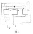
- FIG. 1shows a computer
- FIG. 2shows a forced instruction block module
- FIG. 1shows a block diagram of a computer 14 . Parts of the computer 14 that are not used for describing operation of the invention are not shown.
- FIG. 1shows an instruction execution unit 10 , a request logic circuit 11 , an instruction memory 12 , a forced instruction block module 15 and a communication bus 16 .
- Instruction execution unit 10has an instruction memory enable output coupled to instruction memory 12 and forced instruction block 15 .
- Instruction memory 12has an instruction address input coupled to instruction execution unit 10 via bus 16 .
- Instruction memory 12has an instruction output coupled to forced instruction block module 15 .
- Forced instruction block module 15has an instruction output coupled to instruction execution unit 10 via bus 16 .
- Request logic circuit 11 and forced instruction block module 15have control inputs coupled to a test control unit 19 external to computer 14 .
- FIG. 2shows a forced instruction block module.
- This modulecontains registers 20 a-d , a first and second multiplexer 22 , 24 a counter 26 and a control unit 28 .
- the registers 20 a-bhave outputs coupled to the first multiplexer 22 .
- the second multiplexer 24has inputs coupled to an output of the first multiplexer 22 and the instruction output of the instruction memory 12 (not shown in FIG. 2 ).
- An output of the second multiplexer 24is coupled to the instruction execution unit 10 via bus 16 (both not shown in FIG. 2 ).
- Counter 26has an enable input coupled to the instruction memory enable output of the instruction execution unit 10 .
- Counter 26has a count output coupled to a control input of the first multiplexer 22 .
- Registers 20 a-d and counter 26are part of a scan chain, shown schematically as 29 a .
- a scan chainis part of a well known test technique, which makes all internal flip-flops and registers of a circuit accessible via a shift register).
- Registers 20 a-d and counter 26have scan control inputs coupled to a scan control connection 29 b .
- Control unit 28has an input coupled to the test control unit 19 (not shown in FIG. 2 ).
- Control unit 28has a connection with counter 26 and an output coupled to a control input of the second multiplexer 24 .
- a control signal applied to forced execution clock module 15 and request logic circuit 11may be used to bring the computer in a normal operation mode.
- instruction execution unit 10supplies successive instruction addresses to instruction memory 12 via bus 16 .
- instruction execution unit 10supplies an enable signal to instruction memory 12 when an instruction address is available on bus 16 .
- instruction memory 12delivers the instructions corresponding to the instruction addresses to the instruction execution unit 10 via the second multiplexer 24 of the forced execution block module 15 and the bus 16 .
- Instruction execution unit 10executes these instructions.
- request logic circuit 11In case an asynchronous instruction execution unit 10 is used, the start of execution of each instruction is controlled by means of a handshake between instruction execution unit 10 and request logic circuit 11 . Each time the instruction execution unit 10 is ready to execute a next instruction it supplies a request signal to request logic circuit 11 . In response request logic circuit 11 supplies an acknowledge signal to instruction to instruction execution unit 10 , which causes instruction execution unit 10 to start execution of a next instruction.
- Request logic circuit 11may use information from the handshakes in various ways. For example, request logic circuit 11 may cause a supply voltage to the instruction execution unit 10 to be reduced or increased if request signals arrive faster or slower than necessary for a given task respectively. Reduction of the supply voltage reduces the power consumed by the instruction execution unit 10 .
- the computer 14When the computer 14 is used for a given application, say a telephone handset, it has to be guaranteed that speed and power consumption satisfy certain predetermined specifications. Due to process fluctuations or errors during manufacture of the computer 14 , these parameters may vary. The computer 14 needs to be tested to ensure that the specifications are met. For this reason, the computer 14 has to be tested, by measuring for example the time it takes the instruction execution unit 10 to execute an instruction under test when a given supply voltage is applied to the instruction execution unit 10 . Another test involves measuring the current consumed by the computer 14 when it executes this instruction under test.
- the instruction execution unit 10is forced to execute the instruction under test repeatedly during a time interval and it is measured how many times this instruction is executed during that time interval.
- the number of times that the instruction under test is executedis not fixed by a clock rate, but depends on the speed with which the instruction execution unit 10 returns request signals upon acknowledge signals. Different instructions may be used as instruction under test in successive tests to test different parts of the instruction execution unit 10 . Similarly, the current used by the computer 14 may be measured during repeated execution of the instruction under test.
- the forced instruction block module 15provides for the repeated execution of an instruction under test.
- the test control unit 19applies a control signal to the forced instruction block module 15 to bring it into a test mode.
- the forced instruction block module 15cyclically supplies the content of registers 20 a-d to the instruction execution unit 10 via bus 16 instead of the instruction produced by instruction memory.
- the forced instruction block module 15 shown in FIG. 2is designed for a type of instruction execution unit 10 that uses instructions that may consist of 1, 2, 3 or 4 bytes that are transmitted successively via bus 16 .
- a first step of the testthe bytes that make up the instruction under test, a counter control signal and a control signal to enable the forced instruction execution block 15 are loaded via the scan chain 29 a .
- the forced instruction execution block module 15is made to operate in the test mode.
- the counter 26causes the first multiplexer 22 to pass the content of a cyclical succession of the registers 20 a-b to the second multiplexer 24 .
- the second multiplexer 24passes this content to the bus 16 instead of the instruction from instruction memory 12 .
- this stepit is counted how many times the instruction is executed during a given time interval. As the instruction under test is executed repeatedly the time interval can start and stop at any desired time.
- the counterhas two modes, selected via the scan chain 29 a dependent on the number of bytes contained in the instruction under test.
- the counter 26has a cycle of four, selecting a first, second, third and fourth one of the registers 20 a-d successively and subsequently repeating this selection of these registers 20 a-d cyclically.
- the first modeis used when the instruction under test is one, two or four bytes long. In case of a one byte long instruction under test, four copies of the instruction are loaded into the four registers 20 a-d via the scan chain 29 a .
- the counter 26has a cycle of three, selecting a first, second and third one of the registers 20 a-c successively and subsequently repeating the selection of these three registers 20 a-c cyclically.
- the second modeis used when the instruction under test is three bytes long. The bytes of the instruction are loaded into the three different registers 20 a-d that will be loaded cyclically. Thus only one bit in the scan chain 29 a is needed to select between one, two, three or four byte instructions.
- instruction execution units 10may be used.
- instructionsmay always be supplied in one cycle.
- the counter 26 , first multiplexer 22 and different registers 20 a-dare not needed. Only one register is needed to supply the instruction under test to the second multiplexer 24 .
- Other maximum instruction lengths than four bytesmay be used. More registers 20 a-d than needed for the maximum length instruction may be used in order to make it possible to load and execute different instructions alternately during a test.
- registers 20 a-done could use a small memory, the counter 26 addressing this memory. In this case the first multiplexer 22 may be omitted.
- registers 20 a-dhave the advantage over a memory that they can be incorporated directly in a scan chain. If the execution unit has fixed length instructions, the least significant bits of instruction addresses may be used instead of the output of the counter 26 .
- the forced instruction block module 15may be inserted between the bus 16 and the instruction execution unit 10 , instead of between the instruction memory 12 and the bus.
- execution timecan be measured without delays from the bus.
- execution timecan be measured with and without delays from the bus 16 , which makes it possible to test the delays caused by the bus.
- a forced instruction block module 15may be inserted at other positions in the processor.
- the registers 20 a-dmay be memory mapped, allowing the instruction execution unit 10 to write the instruction under test into the registers 20 a-d .
- the registersmay be treated as special function registers of the instruction execution unit 10 , so that they the instruction execution unit 10 can write the instruction under test into these registers by means of a write to register instruction.
Landscapes
- Engineering & Computer Science (AREA)
- General Engineering & Computer Science (AREA)
- Theoretical Computer Science (AREA)
- Computer Hardware Design (AREA)
- Quality & Reliability (AREA)
- Physics & Mathematics (AREA)
- General Physics & Mathematics (AREA)
- Test And Diagnosis Of Digital Computers (AREA)
- Microcomputers (AREA)
- Debugging And Monitoring (AREA)
Abstract
Description
Claims (15)
Applications Claiming Priority (2)
| Application Number | Priority Date | Filing Date | Title |
|---|---|---|---|
| EP99202948 | 1999-09-10 | ||
| EP99202948 | 1999-09-10 |
Publications (1)
| Publication Number | Publication Date |
|---|---|
| US6728900B1true US6728900B1 (en) | 2004-04-27 |
Family
ID=8240627
Family Applications (1)
| Application Number | Title | Priority Date | Filing Date |
|---|---|---|---|
| US09/656,833Expired - Fee RelatedUS6728900B1 (en) | 1999-09-10 | 2000-09-07 | Microcomputer with test instruction memory |
Country Status (5)
| Country | Link |
|---|---|
| US (1) | US6728900B1 (en) |
| EP (1) | EP1129408B1 (en) |
| JP (1) | JP2003509770A (en) |
| DE (1) | DE60012132T2 (en) |
| WO (1) | WO2001020455A1 (en) |
Cited By (40)
| Publication number | Priority date | Publication date | Assignee | Title |
|---|---|---|---|---|
| US6892322B1 (en)* | 2000-10-26 | 2005-05-10 | Cypress Semiconductor Corporation | Method for applying instructions to microprocessor in test mode |
| US7737724B2 (en) | 2007-04-17 | 2010-06-15 | Cypress Semiconductor Corporation | Universal digital block interconnection and channel routing |
| US7761845B1 (en) | 2002-09-09 | 2010-07-20 | Cypress Semiconductor Corporation | Method for parameterizing a user module |
| US7765095B1 (en) | 2000-10-26 | 2010-07-27 | Cypress Semiconductor Corporation | Conditional branching in an in-circuit emulation system |
| US7770113B1 (en) | 2001-11-19 | 2010-08-03 | Cypress Semiconductor Corporation | System and method for dynamically generating a configuration datasheet |
| US7774190B1 (en) | 2001-11-19 | 2010-08-10 | Cypress Semiconductor Corporation | Sleep and stall in an in-circuit emulation system |
| US7825688B1 (en) | 2000-10-26 | 2010-11-02 | Cypress Semiconductor Corporation | Programmable microcontroller architecture(mixed analog/digital) |
| US7844437B1 (en) | 2001-11-19 | 2010-11-30 | Cypress Semiconductor Corporation | System and method for performing next placements and pruning of disallowed placements for programming an integrated circuit |
| US7893724B2 (en) | 2004-03-25 | 2011-02-22 | Cypress Semiconductor Corporation | Method and circuit for rapid alignment of signals |
| US20110087861A1 (en)* | 2009-10-12 | 2011-04-14 | The Regents Of The University Of Michigan | System for High-Efficiency Post-Silicon Verification of a Processor |
| US8026739B2 (en) | 2007-04-17 | 2011-09-27 | Cypress Semiconductor Corporation | System level interconnect with programmable switching |
| US8040266B2 (en) | 2007-04-17 | 2011-10-18 | Cypress Semiconductor Corporation | Programmable sigma-delta analog-to-digital converter |
| US8049569B1 (en) | 2007-09-05 | 2011-11-01 | Cypress Semiconductor Corporation | Circuit and method for improving the accuracy of a crystal-less oscillator having dual-frequency modes |
| US8067948B2 (en) | 2006-03-27 | 2011-11-29 | Cypress Semiconductor Corporation | Input/output multiplexer bus |
| US8069405B1 (en) | 2001-11-19 | 2011-11-29 | Cypress Semiconductor Corporation | User interface for efficiently browsing an electronic document using data-driven tabs |
| US8069428B1 (en) | 2001-10-24 | 2011-11-29 | Cypress Semiconductor Corporation | Techniques for generating microcontroller configuration information |
| US8069436B2 (en) | 2004-08-13 | 2011-11-29 | Cypress Semiconductor Corporation | Providing hardware independence to automate code generation of processing device firmware |
| US8078970B1 (en) | 2001-11-09 | 2011-12-13 | Cypress Semiconductor Corporation | Graphical user interface with user-selectable list-box |
| US8085100B2 (en) | 2005-02-04 | 2011-12-27 | Cypress Semiconductor Corporation | Poly-phase frequency synthesis oscillator |
| US8085067B1 (en) | 2005-12-21 | 2011-12-27 | Cypress Semiconductor Corporation | Differential-to-single ended signal converter circuit and method |
| US8089461B2 (en) | 2005-06-23 | 2012-01-03 | Cypress Semiconductor Corporation | Touch wake for electronic devices |
| US8092083B2 (en) | 2007-04-17 | 2012-01-10 | Cypress Semiconductor Corporation | Temperature sensor with digital bandgap |
| US8103497B1 (en) | 2002-03-28 | 2012-01-24 | Cypress Semiconductor Corporation | External interface for event architecture |
| US8103496B1 (en) | 2000-10-26 | 2012-01-24 | Cypress Semicondutor Corporation | Breakpoint control in an in-circuit emulation system |
| US8120408B1 (en) | 2005-05-05 | 2012-02-21 | Cypress Semiconductor Corporation | Voltage controlled oscillator delay cell and method |
| US8130025B2 (en) | 2007-04-17 | 2012-03-06 | Cypress Semiconductor Corporation | Numerical band gap |
| US8149048B1 (en) | 2000-10-26 | 2012-04-03 | Cypress Semiconductor Corporation | Apparatus and method for programmable power management in a programmable analog circuit block |
| US8160864B1 (en) | 2000-10-26 | 2012-04-17 | Cypress Semiconductor Corporation | In-circuit emulator and pod synchronized boot |
| US8176296B2 (en) | 2000-10-26 | 2012-05-08 | Cypress Semiconductor Corporation | Programmable microcontroller architecture |
| US8286125B2 (en) | 2004-08-13 | 2012-10-09 | Cypress Semiconductor Corporation | Model for a hardware device-independent method of defining embedded firmware for programmable systems |
| US8402313B1 (en) | 2002-05-01 | 2013-03-19 | Cypress Semiconductor Corporation | Reconfigurable testing system and method |
| US8499270B1 (en) | 2007-04-25 | 2013-07-30 | Cypress Semiconductor Corporation | Configuration of programmable IC design elements |
| US8516025B2 (en) | 2007-04-17 | 2013-08-20 | Cypress Semiconductor Corporation | Clock driven dynamic datapath chaining |
| US8527949B1 (en) | 2001-11-19 | 2013-09-03 | Cypress Semiconductor Corporation | Graphical user interface for dynamically reconfiguring a programmable device |
| US8909960B1 (en) | 2007-04-25 | 2014-12-09 | Cypress Semiconductor Corporation | Power management architecture, method and configuration system |
| US20160188449A1 (en)* | 2013-08-12 | 2016-06-30 | Nec Corporation | Software aging test system, software aging test method, and program for software aging test |
| US9448964B2 (en) | 2009-05-04 | 2016-09-20 | Cypress Semiconductor Corporation | Autonomous control in a programmable system |
| US9564902B2 (en) | 2007-04-17 | 2017-02-07 | Cypress Semiconductor Corporation | Dynamically configurable and re-configurable data path |
| US9720805B1 (en) | 2007-04-25 | 2017-08-01 | Cypress Semiconductor Corporation | System and method for controlling a target device |
| US10698662B2 (en) | 2001-11-15 | 2020-06-30 | Cypress Semiconductor Corporation | System providing automatic source code generation for personalization and parameterization of user modules |
Citations (7)
| Publication number | Priority date | Publication date | Assignee | Title |
|---|---|---|---|---|
| US4870573A (en) | 1985-04-03 | 1989-09-26 | Nec Corporation | Microcomputer capable of testing execution of a program with no branch |
| US4870345A (en)* | 1986-08-04 | 1989-09-26 | Mitsubishi Denki Kabushiki Kaisha | Semiconductor intergrated circuit device |
| US5530804A (en)* | 1994-05-16 | 1996-06-25 | Motorola, Inc. | Superscalar processor with plural pipelined execution units each unit selectively having both normal and debug modes |
| US5706294A (en)* | 1995-07-04 | 1998-01-06 | Ricoh Company, Ltd. | Method of finding DC test point of an integrated circuit |
| US5802071A (en) | 1995-11-17 | 1998-09-01 | Fang; I Liang | Micro-controller with a built-in test circuit and method for testing the same |
| US6106572A (en)* | 1998-03-25 | 2000-08-22 | Origins Software Company | Forward and reverse hierarchical page level debugger |
| US6539498B1 (en)* | 1999-05-06 | 2003-03-25 | Fujitsu Limited | Method of detecting cause of failure in computer |
- 2000
- 2000-08-30DEDE60012132Tpatent/DE60012132T2/ennot_activeExpired - Lifetime
- 2000-08-30JPJP2001523965Apatent/JP2003509770A/ennot_activeWithdrawn
- 2000-08-30WOPCT/EP2000/008447patent/WO2001020455A1/enactiveIP Right Grant
- 2000-08-30EPEP00956500Apatent/EP1129408B1/ennot_activeExpired - Lifetime
- 2000-09-07USUS09/656,833patent/US6728900B1/ennot_activeExpired - Fee Related
Patent Citations (7)
| Publication number | Priority date | Publication date | Assignee | Title |
|---|---|---|---|---|
| US4870573A (en) | 1985-04-03 | 1989-09-26 | Nec Corporation | Microcomputer capable of testing execution of a program with no branch |
| US4870345A (en)* | 1986-08-04 | 1989-09-26 | Mitsubishi Denki Kabushiki Kaisha | Semiconductor intergrated circuit device |
| US5530804A (en)* | 1994-05-16 | 1996-06-25 | Motorola, Inc. | Superscalar processor with plural pipelined execution units each unit selectively having both normal and debug modes |
| US5706294A (en)* | 1995-07-04 | 1998-01-06 | Ricoh Company, Ltd. | Method of finding DC test point of an integrated circuit |
| US5802071A (en) | 1995-11-17 | 1998-09-01 | Fang; I Liang | Micro-controller with a built-in test circuit and method for testing the same |
| US6106572A (en)* | 1998-03-25 | 2000-08-22 | Origins Software Company | Forward and reverse hierarchical page level debugger |
| US6539498B1 (en)* | 1999-05-06 | 2003-03-25 | Fujitsu Limited | Method of detecting cause of failure in computer |
Cited By (56)
| Publication number | Priority date | Publication date | Assignee | Title |
|---|---|---|---|---|
| US9766650B2 (en) | 2000-10-26 | 2017-09-19 | Cypress Semiconductor Corporation | Microcontroller programmable system on a chip with programmable interconnect |
| US8358150B1 (en) | 2000-10-26 | 2013-01-22 | Cypress Semiconductor Corporation | Programmable microcontroller architecture(mixed analog/digital) |
| US8149048B1 (en) | 2000-10-26 | 2012-04-03 | Cypress Semiconductor Corporation | Apparatus and method for programmable power management in a programmable analog circuit block |
| US7765095B1 (en) | 2000-10-26 | 2010-07-27 | Cypress Semiconductor Corporation | Conditional branching in an in-circuit emulation system |
| US8160864B1 (en) | 2000-10-26 | 2012-04-17 | Cypress Semiconductor Corporation | In-circuit emulator and pod synchronized boot |
| US10261932B2 (en) | 2000-10-26 | 2019-04-16 | Cypress Semiconductor Corporation | Microcontroller programmable system on a chip |
| US7825688B1 (en) | 2000-10-26 | 2010-11-02 | Cypress Semiconductor Corporation | Programmable microcontroller architecture(mixed analog/digital) |
| US10248604B2 (en) | 2000-10-26 | 2019-04-02 | Cypress Semiconductor Corporation | Microcontroller programmable system on a chip |
| US10020810B2 (en) | 2000-10-26 | 2018-07-10 | Cypress Semiconductor Corporation | PSoC architecture |
| US9843327B1 (en) | 2000-10-26 | 2017-12-12 | Cypress Semiconductor Corporation | PSOC architecture |
| US10725954B2 (en) | 2000-10-26 | 2020-07-28 | Monterey Research, Llc | Microcontroller programmable system on a chip |
| US8176296B2 (en) | 2000-10-26 | 2012-05-08 | Cypress Semiconductor Corporation | Programmable microcontroller architecture |
| US8103496B1 (en) | 2000-10-26 | 2012-01-24 | Cypress Semicondutor Corporation | Breakpoint control in an in-circuit emulation system |
| US8555032B2 (en) | 2000-10-26 | 2013-10-08 | Cypress Semiconductor Corporation | Microcontroller programmable system on a chip with programmable interconnect |
| US6892322B1 (en)* | 2000-10-26 | 2005-05-10 | Cypress Semiconductor Corporation | Method for applying instructions to microprocessor in test mode |
| US8736303B2 (en) | 2000-10-26 | 2014-05-27 | Cypress Semiconductor Corporation | PSOC architecture |
| US8069428B1 (en) | 2001-10-24 | 2011-11-29 | Cypress Semiconductor Corporation | Techniques for generating microcontroller configuration information |
| US8793635B1 (en) | 2001-10-24 | 2014-07-29 | Cypress Semiconductor Corporation | Techniques for generating microcontroller configuration information |
| US10466980B2 (en) | 2001-10-24 | 2019-11-05 | Cypress Semiconductor Corporation | Techniques for generating microcontroller configuration information |
| US8078970B1 (en) | 2001-11-09 | 2011-12-13 | Cypress Semiconductor Corporation | Graphical user interface with user-selectable list-box |
| US10698662B2 (en) | 2001-11-15 | 2020-06-30 | Cypress Semiconductor Corporation | System providing automatic source code generation for personalization and parameterization of user modules |
| US8069405B1 (en) | 2001-11-19 | 2011-11-29 | Cypress Semiconductor Corporation | User interface for efficiently browsing an electronic document using data-driven tabs |
| US8533677B1 (en) | 2001-11-19 | 2013-09-10 | Cypress Semiconductor Corporation | Graphical user interface for dynamically reconfiguring a programmable device |
| US7770113B1 (en) | 2001-11-19 | 2010-08-03 | Cypress Semiconductor Corporation | System and method for dynamically generating a configuration datasheet |
| US8527949B1 (en) | 2001-11-19 | 2013-09-03 | Cypress Semiconductor Corporation | Graphical user interface for dynamically reconfiguring a programmable device |
| US7844437B1 (en) | 2001-11-19 | 2010-11-30 | Cypress Semiconductor Corporation | System and method for performing next placements and pruning of disallowed placements for programming an integrated circuit |
| US7774190B1 (en) | 2001-11-19 | 2010-08-10 | Cypress Semiconductor Corporation | Sleep and stall in an in-circuit emulation system |
| US8370791B2 (en) | 2001-11-19 | 2013-02-05 | Cypress Semiconductor Corporation | System and method for performing next placements and pruning of disallowed placements for programming an integrated circuit |
| US8103497B1 (en) | 2002-03-28 | 2012-01-24 | Cypress Semiconductor Corporation | External interface for event architecture |
| US8402313B1 (en) | 2002-05-01 | 2013-03-19 | Cypress Semiconductor Corporation | Reconfigurable testing system and method |
| US7761845B1 (en) | 2002-09-09 | 2010-07-20 | Cypress Semiconductor Corporation | Method for parameterizing a user module |
| US7893724B2 (en) | 2004-03-25 | 2011-02-22 | Cypress Semiconductor Corporation | Method and circuit for rapid alignment of signals |
| US8069436B2 (en) | 2004-08-13 | 2011-11-29 | Cypress Semiconductor Corporation | Providing hardware independence to automate code generation of processing device firmware |
| US8286125B2 (en) | 2004-08-13 | 2012-10-09 | Cypress Semiconductor Corporation | Model for a hardware device-independent method of defining embedded firmware for programmable systems |
| US8085100B2 (en) | 2005-02-04 | 2011-12-27 | Cypress Semiconductor Corporation | Poly-phase frequency synthesis oscillator |
| US8120408B1 (en) | 2005-05-05 | 2012-02-21 | Cypress Semiconductor Corporation | Voltage controlled oscillator delay cell and method |
| US8089461B2 (en) | 2005-06-23 | 2012-01-03 | Cypress Semiconductor Corporation | Touch wake for electronic devices |
| US8085067B1 (en) | 2005-12-21 | 2011-12-27 | Cypress Semiconductor Corporation | Differential-to-single ended signal converter circuit and method |
| US8067948B2 (en) | 2006-03-27 | 2011-11-29 | Cypress Semiconductor Corporation | Input/output multiplexer bus |
| US8717042B1 (en) | 2006-03-27 | 2014-05-06 | Cypress Semiconductor Corporation | Input/output multiplexer bus |
| US8516025B2 (en) | 2007-04-17 | 2013-08-20 | Cypress Semiconductor Corporation | Clock driven dynamic datapath chaining |
| US7737724B2 (en) | 2007-04-17 | 2010-06-15 | Cypress Semiconductor Corporation | Universal digital block interconnection and channel routing |
| US8040266B2 (en) | 2007-04-17 | 2011-10-18 | Cypress Semiconductor Corporation | Programmable sigma-delta analog-to-digital converter |
| US8092083B2 (en) | 2007-04-17 | 2012-01-10 | Cypress Semiconductor Corporation | Temperature sensor with digital bandgap |
| US8130025B2 (en) | 2007-04-17 | 2012-03-06 | Cypress Semiconductor Corporation | Numerical band gap |
| US8476928B1 (en) | 2007-04-17 | 2013-07-02 | Cypress Semiconductor Corporation | System level interconnect with programmable switching |
| US9564902B2 (en) | 2007-04-17 | 2017-02-07 | Cypress Semiconductor Corporation | Dynamically configurable and re-configurable data path |
| US8026739B2 (en) | 2007-04-17 | 2011-09-27 | Cypress Semiconductor Corporation | System level interconnect with programmable switching |
| US8499270B1 (en) | 2007-04-25 | 2013-07-30 | Cypress Semiconductor Corporation | Configuration of programmable IC design elements |
| US9720805B1 (en) | 2007-04-25 | 2017-08-01 | Cypress Semiconductor Corporation | System and method for controlling a target device |
| US8909960B1 (en) | 2007-04-25 | 2014-12-09 | Cypress Semiconductor Corporation | Power management architecture, method and configuration system |
| US8049569B1 (en) | 2007-09-05 | 2011-11-01 | Cypress Semiconductor Corporation | Circuit and method for improving the accuracy of a crystal-less oscillator having dual-frequency modes |
| US9448964B2 (en) | 2009-05-04 | 2016-09-20 | Cypress Semiconductor Corporation | Autonomous control in a programmable system |
| US20110087861A1 (en)* | 2009-10-12 | 2011-04-14 | The Regents Of The University Of Michigan | System for High-Efficiency Post-Silicon Verification of a Processor |
| US9858176B2 (en)* | 2013-08-12 | 2018-01-02 | Nec Corporation | Software aging test system, software aging test method, and program for software aging test |
| US20160188449A1 (en)* | 2013-08-12 | 2016-06-30 | Nec Corporation | Software aging test system, software aging test method, and program for software aging test |
Also Published As
| Publication number | Publication date |
|---|---|
| WO2001020455A1 (en) | 2001-03-22 |
| EP1129408B1 (en) | 2004-07-14 |
| DE60012132D1 (en) | 2004-08-19 |
| EP1129408A1 (en) | 2001-09-05 |
| DE60012132T2 (en) | 2005-08-25 |
| JP2003509770A (en) | 2003-03-11 |
Similar Documents
| Publication | Publication Date | Title |
|---|---|---|
| US6728900B1 (en) | Microcomputer with test instruction memory | |
| KR100492205B1 (en) | Built-In Self-Test Configuration of Integrated Circuit Memory Devices | |
| US6760865B2 (en) | Multiple level built-in self-test controller and method therefor | |
| US6347056B1 (en) | Recording of result information in a built-in self-test circuit and method therefor | |
| US5345580A (en) | Microprocessor device and emulator device thereof | |
| US6523136B1 (en) | Semiconductor integrated circuit device with processor | |
| CA1145852A (en) | Diagnostic circuitry in a data processor | |
| EP0042222A2 (en) | Programmable sequence generator for in-circuit digital tester | |
| US6181151B1 (en) | Integrated circuit tester with disk-based data streaming | |
| US5673271A (en) | High speed pattern generator | |
| US5475852A (en) | Microprocessor implementing single-step or sequential microcode execution while in test mode | |
| JP2001148199A5 (en) | ||
| EP0729088B1 (en) | Single chip microcomputer having a plurality of timer counters | |
| US6009546A (en) | Algorithmic pattern generator | |
| US20020174394A1 (en) | External control of algorithm execution in a built-in self-test circuit and method therefor | |
| US6543019B2 (en) | Method for built-in self test of an electronic circuit | |
| US6061815A (en) | Programming utility register to generate addresses in algorithmic pattern generator | |
| US4636945A (en) | Microprocessor | |
| US6948086B2 (en) | Computer system | |
| KR100277770B1 (en) | Sequence control circuit | |
| US20040177300A1 (en) | Apparatus with a test interface | |
| US6948097B2 (en) | Semiconductor device including function verification capability | |
| TWI783898B (en) | Test circuit and method for reading data from a memory device during memory dump | |
| US20230314513A1 (en) | In-circuit emulator device | |
| JPH0894724A (en) | Pattern generator for lsi testing device |
Legal Events
| Date | Code | Title | Description |
|---|---|---|---|
| AS | Assignment | Owner name:U.S. PHILIPS CORPORATION, NEW YORK Free format text:ASSIGNMENT OF ASSIGNORS INTEREST;ASSIGNOR:MELI, LOUIS MARCEL;REEL/FRAME:011282/0383 Effective date:20001009 | |
| AS | Assignment | Owner name:KONINKLIJKE PHILIPS ELECTRONICS N.V., NETHERLANDS Free format text:ASSIGNMENT OF ASSIGNORS INTEREST;ASSIGNOR:U.S. PHILIPS CORPORATION;REEL/FRAME:015060/0067 Effective date:20040308 | |
| AS | Assignment | Owner name:NXP B.V., NETHERLANDS Free format text:ASSIGNMENT OF ASSIGNORS INTEREST;ASSIGNOR:KONINKLIJKE PHILIPS ELECTRONICS N.V.;REEL/FRAME:018635/0787 Effective date:20061117 | |
| FPAY | Fee payment | Year of fee payment:4 | |
| FEPP | Fee payment procedure | Free format text:PAT HOLDER CLAIMS SMALL ENTITY STATUS, ENTITY STATUS SET TO SMALL (ORIGINAL EVENT CODE: LTOS); ENTITY STATUS OF PATENT OWNER: SMALL ENTITY | |
| REFU | Refund | Free format text:REFUND - PAYMENT OF MAINTENANCE FEE, 8TH YEAR, LARGE ENTITY (ORIGINAL EVENT CODE: R1552); ENTITY STATUS OF PATENT OWNER: SMALL ENTITY | |
| FPAY | Fee payment | Year of fee payment:8 | |
| FEPP | Fee payment procedure | Free format text:PAYER NUMBER DE-ASSIGNED (ORIGINAL EVENT CODE: RMPN); ENTITY STATUS OF PATENT OWNER: SMALL ENTITY Free format text:PAYOR NUMBER ASSIGNED (ORIGINAL EVENT CODE: ASPN); ENTITY STATUS OF PATENT OWNER: SMALL ENTITY | |
| AS | Assignment | Owner name:DSP GROUP SWITZERLAND AG, SWITZERLAND Free format text:ASSIGNMENT OF ASSIGNORS INTEREST;ASSIGNOR:NXP B.V.;REEL/FRAME:028293/0451 Effective date:20070904 | |
| REMI | Maintenance fee reminder mailed | ||
| LAPS | Lapse for failure to pay maintenance fees | ||
| STCH | Information on status: patent discontinuation | Free format text:PATENT EXPIRED DUE TO NONPAYMENT OF MAINTENANCE FEES UNDER 37 CFR 1.362 | |
| FP | Lapsed due to failure to pay maintenance fee | Effective date:20160427 |