Movatterモバイル変換


[0]ホーム

URL:


US6728325B1 - Method and apparatus for mixing down and spectrum folding frequency diverse modulated carrier - Google Patents

Method and apparatus for mixing down and spectrum folding frequency diverse modulated carrier
Download PDF

Info

Publication number
US6728325B1
US6728325B1US09/497,030US49703000AUS6728325B1US 6728325 B1US6728325 B1US 6728325B1US 49703000 AUS49703000 AUS 49703000AUS 6728325 B1US6728325 B1US 6728325B1
Authority
US
United States
Prior art keywords
frequency
series
samples
sine wave
modulated carrier
Prior art date
Legal status (The legal status is an assumption and is not a legal conclusion. Google has not performed a legal analysis and makes no representation as to the accuracy of the status listed.)
Expired - Fee Related
Application number
US09/497,030
Inventor
Chien-Meen Hwang
Eugen Gershon
Current Assignee (The listed assignees may be inaccurate. Google has not performed a legal analysis and makes no representation or warranty as to the accuracy of the list.)
Microsemi Semiconductor US Inc
Original Assignee
Legerity Inc
Priority date (The priority date is an assumption and is not a legal conclusion. Google has not performed a legal analysis and makes no representation as to the accuracy of the date listed.)
Filing date
Publication date
Priority to US09/497,030priorityCriticalpatent/US6728325B1/en
Assigned to ADVANCED MICRO DEVICES, INC.reassignmentADVANCED MICRO DEVICES, INC.ASSIGNMENT OF ASSIGNORS INTEREST (SEE DOCUMENT FOR DETAILS).Assignors: GERSHON, EUGEN, HWANG, CHIEN-MEEN
Application filed by Legerity IncfiledCriticalLegerity Inc
Assigned to MORGAN STANLEY & CO. INCORPORATEDreassignmentMORGAN STANLEY & CO. INCORPORATEDSECURITY INTEREST (SEE DOCUMENT FOR DETAILS).Assignors: LEGERITY, INC.
Assigned to LEGERITY, INC.reassignmentLEGERITY, INC.ASSIGNMENT OF ASSIGNORS INTEREST (SEE DOCUMENT FOR DETAILS).Assignors: ADVANCED MICRO DEVICES, INC.
Assigned to MORGAN STANLEY & CO. INCORPORATED, AS FACILITY COLLATERAL AGENTreassignmentMORGAN STANLEY & CO. INCORPORATED, AS FACILITY COLLATERAL AGENTSECURITY AGREEMENTAssignors: LEGERITY HOLDINGS, INC., LEGERITY INTERNATIONAL, INC., LEGERITY, INC.
Application grantedgrantedCritical
Publication of US6728325B1publicationCriticalpatent/US6728325B1/en
Assigned to LEGERITY, INC.reassignmentLEGERITY, INC.RELEASE BY SECURED PARTY (SEE DOCUMENT FOR DETAILS).Assignors: MORGAN STANLEY SENIOR FUNDING INC
Assigned to Microsemi Semiconductor (U.S.) Inc.reassignmentMicrosemi Semiconductor (U.S.) Inc.CHANGE OF NAME (SEE DOCUMENT FOR DETAILS).Assignors: ZARLINK SEMICONDUCTOR (U.S.) INC.
Assigned to ZARLINK SEMICONDUCTOR (U.S.) INC.reassignmentZARLINK SEMICONDUCTOR (U.S.) INC.MERGER (SEE DOCUMENT FOR DETAILS).Assignors: LEGERITY, INC.
Assigned to MORGAN STANLEY & CO. LLCreassignmentMORGAN STANLEY & CO. LLCPATENT SECURITY AGREEMENTAssignors: Microsemi Semiconductor (U.S.) Inc.
Assigned to BANK OF AMERICA, N.A., AS SUCCESSOR AGENTreassignmentBANK OF AMERICA, N.A., AS SUCCESSOR AGENTNOTICE OF SUCCESSION OF AGENCYAssignors: ROYAL BANK OF CANADA (AS SUCCESSOR TO MORGAN STANLEY & CO. LLC)
Assigned to MICROSEMI CORPORATION, MICROSEMI COMMUNICATIONS, INC. (F/K/A VITESSE SEMICONDUCTOR CORPORATION), A DELAWARE CORPORATION, MICROSEMI CORP.-MEMORY AND STORAGE SOLUTIONS (F/K/A WHITE ELECTRONIC DESIGNS CORPORATION), AN INDIANA CORPORATION, MICROSEMI FREQUENCY AND TIME CORPORATION, A DELAWARE CORPORATION, MICROSEMI SOC CORP., A CALIFORNIA CORPORATION, MICROSEMI SEMICONDUCTOR (U.S.) INC., A DELAWARE CORPORATION, MICROSEMI CORP.-ANALOG MIXED SIGNAL GROUP, A DELAWARE CORPORATIONreassignmentMICROSEMI CORPORATIONRELEASE BY SECURED PARTY (SEE DOCUMENT FOR DETAILS).Assignors: BANK OF AMERICA, N.A.
Anticipated expirationlegal-statusCritical
Expired - Fee Relatedlegal-statusCriticalCurrent

Links

Images

Classifications

Definitions

Landscapes

Abstract

A demodulation circuit for demodulating a frequency diverse complex modulated carrier comprises an A/D converter generating a series of samples representing the modulated carrier, a mixer operating to mix the series of samples with a sine wave of one fourth the sampling frequency represented by a series of sine wave values occurring at the sampling frequency, and a decimation filter operating at a decimation factor equal to the sampling frequency divided by the frequency difference between adjacent sub-spectra for folding the sub-spectra and retaining a portion of the mixed down series of samples.

Description

TECHNICAL FIELD
The present invention relates generally to network interfacing, and more particularly, to an apparatus and method for mixing down and spectrum folding a frequency diverse modulated carrier to baseband in a network communications receiver.
BACKGROUND OF THE INVENTION
The transmission of various types of digital data between computers continues to grow in importance. The predominant method of transmitting such digital data includes coding the digital data into a low frequency baseband data signal and modulating the baseband data signal onto a high frequency carrier signal. The high frequency carrier signal is then transmitted across a network physical transmission medium such as electrical cable, fiber optic, RF, or other medium to a remote computing station.
At the remote computing station, the high frequency carrier signal must be received and demodulated to recover the original baseband signal. In the absence of any distortion across the network medium, the received signal would be identical in phase, amplitude, and frequency to the transmitted carrier and could be demodulated using known mixing techniques to recover the baseband signal. The baseband signal could then be recovered into digital data using known sampling algorithms.
One problem with such networks is that the physical medium and network topology tend to distort the high frequency carrier signal. Branch connections and different lengths of such branches cause reflections of the transmitted signal. Such problems are even more apparent in a network which uses home telephone wiring cables as the network physical medium. The typical wiring of the telephone network is designed for the “plain old telephone service” (POTS) signals in the 3-10 kilohertz frequency and are not designed for transmission of high frequency carrier signals in a frequency range greater than 1 MHz. The high frequency carrier signal is also distorted by transients in wiring characteristics due to on-hook and off-hook switching and noise pulses of the POTS (e.g. ringing). The high frequency carrier is further distorted by spurious noise caused by electrical devices operating in close proximity to the “cable” medium.
Such distortion of frequency, amplitude, and phase of the high frequency carrier signal degrades network performance and tends to impede the design of higher data rate networks. Known techniques for compensating for such distortion and improving the data rate of a network include complex modulation schemes and frequency diversity.
Utilizing a complex modulation scheme such as quadrature amplitude modulation (QAM), both the amplitude and phase of the high frequency carrier are modulated to represent I and Q components of a baseband signal. Referring to FIG. 1, a 4-QAM modulation constellation10 is shown. In operation, each data symbol is represented by an I-value of +1 or −1 and a Q-value of +1 or −1 such that the data symbol can be represented by one of the four states12(a)-(d) inconstellation10. Each constellation pointy12(a)-12(d) represents a unique combination of carrier amplitude and phase. For example, constellation point12(a) represents a carrier amplitude of14 and acarrier phase16.
FIG. 2 illustrates the utilization of frequency diversity by transmitting the same data in three mutually exclusive sub-spectra18(a)-(c) of thetransmission band20. Therefore, if a portion of the band is distorted (e.g. one or more of the sub-spectra18(a)-(c)), the data may still be recovered at the receiver from a less distorted portion of the sub-spectra18(a)-(c). For example, a data signal modulated onto a 7 MHz carrier utilizing 6 MHz of bandwidth may include three mutually exclusive sub-bands18(a)-(c) centered at 5 MHz, 7 MHz and 9 MHz.
One approach to demodulating such complex signals is to use filters implemented by digital signal processing (DSP), which provides for a convenient way of varying filter coefficients for each transmission to accommodate carrier distortion as detected in the particular time frame in which the data is being transmitted. Using such approach, the receiver compares the distorted received signal representing a known preamble transmission (prior to the data transmission) to the undistorted waveform of the preamble and determines the appropriate filter coefficients for recovery of the received signal. Such filter coefficients are then used for receiving the data transmission.
In accordance with DSP technology, the high frequency carrier is typically sampled with an A/D converter at a rate that is at least 4 times the carrier frequency. Assuming a carrier frequency on the order of 7 MHz, the sampling rate will be on the order of 30 MHz. A problem associated with processing digital samples at such rates to demodulate a complex modulated carrier, and to process mutually exclusive sub-bands of a frequency diverse system, is that very large and costly digital signal processing systems would be required. Therefore, based on recognized industry goals for size and cost reductions, what is needed is a device and method for recovering data signals from a received modulated carrier that do not suffer from the complexity disadvantages of known systems.
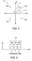
SUMMARY OF THE INVENTION
A first objective of the present invention is to provide a demodulation circuit comprising: a) an A/D converter running at a sampling frequency and generating a series of samples representing a frequency diverse modulated carrier; b) a mixer operating to mix the series of samples with a sine wave of one fourth the sampling frequency, represented by a series of sine wave values occurring at the sampling frequency, the mixer generates a mixed down signal of a series of samples occurring at the sampling frequency; and c) a decimation filter operating at a decimation factor equal to the sampling frequency divided by the frequency difference between adjacent sub-spectra for folding the sub-spectra and retaining a portion of the mixed down series of samples. The portion of the mixed down series of samples may occur at a slow sampling rate equal to the sampling rate divided by the decimation factor of the decimation filter.
The sine wave may have the same frequency as the modulated carrier such that the mixed down series of samples represents the original frequency diverse baseband signal. Alternatively, the sine wave may have a frequency other than that of the modulated carrier and the circuit may further comprise a second mixer operating to mix the portion of the mixed down series of samples with a second sine wave represented by a second series of sine wave values occurring at the slow sampling rate, the second mixer generating the baseband signal.
The mixed down series of samples may represent the I-channel of a system having complex constellation points. The system may further comprise: d) a Q-channel mixer operating to mix the series of samples with a cosine wave of one fourth the sampling frequency represented by a series of cosine wave values occurring at the sampling frequency, the Q-channel mixer generating a mixed down series of samples occurring at the sampling frequency; and e) a Q-channel decimation filter operating at a decimation factor equal to the sampling frequency divided by the frequency difference between adjacent sub-spectra for folding the sub-spectra and retaining a portion of the mixed down series of samples. Both the sine wave and the cosine wave may have the same frequency as the modulated carrier such that both the sine mixed down series of samples and the cosine mixed down series of samples represent the I-channel and the Q-channel of a frequency diverse baseband signal respectively. Alternatively, both the sine wave and the cosine wave may have a frequency other than that of the modulated carrier and the circuit may further comprise: f) a second mixer operating to mix the portion of the mixed down series of samples with a second sine wave represented by a second series of sine wave values occurring at the slow sampling rate, the second mixer generating a baseband signal; and g) a second Q-channel mixer operating to mix the portion of the cosine mixed down series of samples with a second cosine wave represented by a second series of cosine wave values occurring at the slow sampling rate, the second Q-channel mixer generating a baseband Q-channel signal.
Preferably, the sample frequency is 32 MHz, both the sine wave and the cosine wave have a frequency of 8 MHz, the decimation filter has a decimation factor of 16:1, and both the second sine wave and the second cosine wave have a frequency of 1 MHz.
A second objective of the present invention is to provide a method of folding adjacent sub-spectra of a frequency diverse modulated carrier signal, the method comprising: (a) selecting a sample frequency that is a multiple of the difference between adjacent sub-spectra; (b) sampling the modulated carrier at the sampling frequency to generate a series of samples; and (c) decimating the series of samples utilizing a decimation filter with a decimation factor equal to the sample frequency divided the difference between adjacent sub-spectra to generate a decimated series of samples. The method may further comprise mixing the series of samples with a sine wave with a frequency equal to that of the modulated carrier and represented by a series of values occurring at the sample frequency to down mix the modulated carrier to a baseband signal. The method may further yet include mixing the decimated series of samples with a second sine represented by a series of values occurring at the same frequency as that of the decimated series of samples to mix the decimated series of samples to baseband.
BRIEF DESCRIPTION OF THE DRAWINGS
FIG. 1 is a diagram of a complex modulation constellation useful in the practice of the present invention;
FIG. 2 is a frequency domain diagram of a frequency diverse signal useful in the practice of the present invention;
FIG. 3 is a block diagram of a first embodiment of a device for recovery of baseband signals in accordance with the present invention;
FIG. 4 is a flowchart showing a method of determining the phase of a decimation filter in accordance with one embodiment of this invention;
FIG. 5 is a time domain diagram showing a method of determining the phase of a decimation filter in accordance with one embodiment of this invention; and
FIG. 6 is a block diagram of a second embodiment of a device for recovery of baseband signals in accordance with the present invention.
DESCRIPTION OF THE PREFERRED EMBODIMENTS
The present invention will now be described in detail with reference to the drawings. In the drawings, like reference numerals are used to refer to like elements throughout.
Referring to FIG. 3, a block diagram of a first embodiment of adevice30 of this invention for recovering baseband I and Q-signals from a frequency diverse quadrature amplitude modulated (QAM) carrier is shown.Device30 includesanalog front end32 which includes known analog circuits tuned to the modulated carrier frequency for receiving a carrier signal from the transmission medium and amplifying such signal as appropriate for sampling by ANDconverter34. In the preferred embodiment A/D converter34 is an 10-bit A/D converter. In this first embodiment, the A/D converter34 is driven by asampling clock signal36 with a frequency that is four-times that of the modulated carrier frequency. The output of the A/D converter34 is adigitized carrier signal38 comprising a sequence of 10-bit sample values at a sample frequency that is four-times that of the modulated carrier frequency (e.g. a 7 MHz modulated carrier is sampled by an A/D converter clocked at 28 MHz such that thedigitized carrier signal38 is a sequence of sample values at a rate of 28 MHz). The digitizedcarrier signal38 is then processed by ademodulator40 for recovery of the baseband I and Q-signals42(a) and42(b), respectively, in accordance with a first embodiment of this invention.
Thedemodulator40 includesmixer44 for separating the I and Q-channels from the digitizedcarrier signal38.Mixer44 includes an I-channel mixer48(a) which mixes thedigitized carrier signal38 with a sequence of values representing a digitized sine wave46(a). In this first embodiment, the digitized sine wave46(a) has a frequency equal to the carrier frequency such that mixer48(a) mixes the digitizedcarrier signal38 down to a frequency diverse baseband signal50(a). Because the present invention uses digital signal processing, the digitized sine wave46(a) must be represented by a sequence of digital values clocked at the same frequency as the sample frequency (e.g. four-times the modulated carrier frequency) such that mixer48(a) is simply a multiplier. It should be appreciated that the digitized sine wave46(a) can be represented by a repetitive sequence of values [1,0,−1,0] clocked at four-times the digitized sine wave46(a) frequency. As such, the DSP hardware for performing the multiplication can be significantly simplified. For example, in this first embodiment a 7 MHz modulated carrier is represented by a series of samples clocked at 28 MHz and is mixed down by mixing with a 7 MHz digitized sine wave represented by a repetitive sequence of [1,0,−1,0] which is also clocked at 28 MHz.
The frequency diverse baseband signal50(a) is input to a decimation filter52(a). The purpose of the decimation filter52(a) is to reduce the sample frequency and fold the three mutually exclusive sub-spectra18(a)-(c) (FIG. 2) to the baseband I-signal42(a). It should be appreciated that a sampling frequency that matches the frequency difference between the centers of the three sub-spectra18(a)-(c) (FIG. 2) will cause the folding the frequency diverse baseband signal50(a) into the baseband I-signal42(a). Therefore, wherein the centers of the three sub-spectra18(a),18(b), and18(c) are at 5 MHz, 7 MHz, and 9 MHz respectively, a sampling frequency of 2 MHz will achieve the desired folding.
As such, in the first embodiment wherein the frequency diverse baseband signal50(a) is a series of samples clocked at a 28 MHz sampling frequency and the sampling frequency needed for folding the three sub-spectra is a 2 MHz series of values, the decimation filter52(a) must operate at a 14:1 decimation factor such that the output is the baseband I-signal42(a) represented as a series of samples clocked at 2 MHz.
In operation, decimation filter52(a) functions to pass every 14thvalue and ignore the remaining values and as such converts a 28 MHz sample frequency to a 2 MHz sample frequency. It should be appreciated that the output of the decimation filter52(a) will have a better signal to noise ratio if the phase of the decimation filter52(a) is in phase with the local maxima and minima of the frequency diverse baseband signal50(a). Or, stated another way, that the retained values are generally aligned with the peaks and troughs of the frequency diverse baseband signal50(a) and the non-peak and non-trough values are the values that are ignored or decimated. It should be appreciated that because the frequency diverse baseband signal50(a) is baseband, the period of the frequency diverse baseband signal50(a) matches the period of the data symbols communicated thereon.
Referring to the flowchart of FIG.4 and the diagram of FIG. 5, a method for setting the phase of the decimation filter52(a) is shown. Samples60(a)-(e) are in a retained phase group62(2) while the remaining samples are in the decimated phase groups. The decimation filter has a total quantity of phase groups62(1)-(14) that matches the decimation factor (e.g. 14:1) such that samples in the retained phase group (e.g. samples60(a)-(e) in the phase group62(2)) may be retained while the samples in the remaining phase groups are decimated.
Atstep64, asample time period72 is selected. Thesample time period72 is the period in which sample values are analyzed to select the retained phase group.
Atstep66, each sample is determined to be in one of the phase groups62(1)-62(14). Next, atstep68, a sum-of-the-squares value is calculated for each phase group62(1)-(14). The sum-of-the-squares value or each phase group62(1)-(14) is equal to the summation of the square of the value of each sample in the sample period that is in that particular phase group.
Atstep70, the sum-of-the-squares value for each phase group is compared to the other phase groups and the phase group with the highest sum-of-the-squares value is selected as the retained phase group. In the example of FIG. 5, phase group62(2) would have the highest sum of the squares value and is therefore becomes the retained phase group while the remaining phase groups are ignored.
The above described systems and methods effectively recover a baseband I-signal from a frequency diverse QAM carrier signal. Referring again to FIG. 3, the systems and methods for recovery of the baseband Q-signal42(b) are identical to the above described systems and method for recovery of the baseband I-signal42(a) except that thedigitized carrier signal38 is mixed down with a digital cosine waveform at the carrier frequency rather than the digitized sine waveform used for recovery of the baseband I-signal42(a). More specifically, digitizedcarrier signal38 is fed to mixer48(b) which functions identically to mixer48(a) except that it operates to mix digitizedcarrier signal38 with a digitized cosine signal46(b) to yield frequency diverse baseband signal50(b). Frequency diverse baseband signal50(b) is fed to a decimation filter52(b) which functions identically to the decimation filter52(a) to fold the sub-spectra of frequency diverse baseband signal50(b) into baseband Q-signal42(b).
In a second embodiment of this invention it is recognized that, because of various design considerations, it is not always preferable to sample the modulated carrier at four-times the carrier frequency. FIG. 6 shows a second embodiment of adevice30′ wherein the modulated carrier is sampled by A/D converter34′ at a sampling frequency that is greater than four-times that of the modulated carrier. More specifically,device30′ includes analogfront end32 which, like in the first embodiment, includes known analog circuits tuned to the modulated carrier frequency for receiving a carrier signal from a transmission medium and amplifying such signal as appropriate for sampling by A/D converter34′. Again, A/D converter34′ is preferably a 10-bit A/D converter and, in this exemplary embodiment wherein the modulated carrier is a 7 MHz signal, the A/D converter is driven by a 32MHz clock signal36′ such that the output of the A/D converter34′ is adigitized carrier signal38′ comprising a sequence of 10-bit sample values clocked at a sampling frequency of 32 MHz. Thedigitized carrier signal38′ is then coupled to ademodulator40′ for recovery of the baseband I and Q-signals42(a) and42(b) in accordance with this second embodiment of this invention.
Thedemodulator40′ includesmixer44′ for separating the I and Q-channels from the digitizedcarrier signal38′.Mixer44′ includes an I-channel mixer48(a)′ which mixes thedigitized carrier signal38′ with a sequence of values representing a digitized sine wave46(a)′. In this second embodiment, the digitized sine wave46(a)′ has a frequency equal to one-fourth that of the sample frequency such that the digitized sine wave46(a)′ may be represented by a sequence of digital values [1,0,−1,0] clocked at the sample frequency. For example, an 8 MHz sine wave can be represented by the sequence of digital values [1,0,−1,0] clocked at 32 MHz which matches the sample frequency such that mixer48(a)′ is a hardware simple multiplier. It should be appreciated that in this second embodiment, the output of mixer48(a)′ is not the frequency diverse baseband signal because it has been mixed down by 8 MHz as where recovery of baseband requires mixing down by 7 MHz and as such will be called the frequency diverse mixed down signal50(a)′.
The frequency diverse mixed down signal50(a)′ is input to a decimation filter52(a)′. Again, the purpose of the decimation filter52(a)′ is to reduce the sample frequency and fold the three mutually exclusive sub-spectrums18(a)-(c) (FIG. 2) together. Again, a sampling frequency that matches the frequency difference between the centers of the three sub-spectrums18(a)-(c) will result in the folding of the three sub-spectrums in the frequency diverse mixed down signal50(a)′ into an I-channel mixed down signal54(a). As such, in the preferred embodiment where the centers of the three sub-spectra18(a),18(b), and18(c) are at 5 MHz, 7 MHz, and 9 MHz respectively, a sampling frequency of 2 MHz will achieve the desired folding. To achieve a 2 MHz sampling rate, the decimation filter will operate at a 16:1 decimation factor.
Similar to the first embodiment, it should be appreciated that the output of the decimation filter52(a)′ will be a stronger signal if the decimation is in phase with the local maxima and minima of the frequency diverse mixed down signal50(a)′. As such, the same method for selecting a decimation phase as previously discussed with respect to FIGS. 4 and 5 will be used to set the phase of decimation filter52(a)′ in this second embodiment. It should be appreciated that because frequency diverse mixed down signal50(a)′ is not baseband, the period of the signal will be other than the period of the data symbols communicated thereon.
The I-channel mixed down signal54(a) is fed to a second I-channel mixer56(a). As previously discussed, in this second embodiment, the I-channel mixed down signal54(a) is not a baseband signal because it was mixed down by an 8 MHz digitized sine wave46(a)′ rather than by a 7 MHz sine wave (e.g. matching the carrier frequency) that would have mixed down thedigitized carrier signal38 to baseband. To recover baseband in this second embodiment, the I-channel mixed down signal54(a) will need to be mixed up with a 1 MHz digitized sine wave by the second I-channel mixer56(a).
Because the I-channel mixed down signal54(a) has a 2 MHz sampling frequency, the 1 MHz digitized sine wave also must be represent by a 2 MHz sequence of values, which would be a repetitive sequence of [1,−1]. The output of second mixer56(a) is thus the baseband I-signal42(a).
Again, the above described systems and methods of this second embodiment effectively recover a baseband I-signal42(a) from a frequency diverse QAM carrier signal. The systems and methods for recovery of the baseband Q-signal42(b) are identical to the above described systems and method for recovery of the baseband I-signal42(a) except that thedigitized carrier signal38′ is mixed down with a one-fourth sampling frequency digitized cosine wave46(b)′ rather than the one-fourth sampling frequency digitized sine wave46(a)′ used to mix down the I-channel. More specifically, digitizedcarrier signal38′ is fed to mixer48(b)′ which functions identically to mixer48(a)′ except that it operates to mix digitizedcarrier signal38′ with a digitized cosine signal46(b)′ to yield frequency diverse base mixed down signal50(b)′. Frequency diverse mixed down signal50(b)′ is fed to a decimation filter52(b)′ which functions identically to decimation filter52(a)′ to fold the sub-spectra of frequency diverse mixed down signal50(b)′ to yield a Q-channel mixed down signal54(b). The Q-channel mixed down signal54(b) is fed to a second Q-channel mixer56(b) wherein the Q-channel mixed down signal54(b) is mixed with a 1 MHz digitized cosine wave, represented by a repetitive sequence [−1,1] clocked at 2 MHz, to yield the baseband Q-signal42(b)′.
The above described systems and methods provide for a DSP implementation of spectrum folding and reduction of a high frequency sampling rate to a significantly lower sampling rate, and provide for demodulating a frequency diverse modulated data signal with reduction in hardware complexity and size over known systems. Although the invention has been shown and described with respect to certain preferred embodiments, it is obvious that equivalents and modifications will occur to others skilled in the art upon the reading and understanding of the specification. The present invention includes all such equivalents and modifications, and is limited only by the scope of the following claims.

Claims (11)

What is claimed is:
1. A demodulation circuit comprising:
a) an A/D converter, running at a sampling frequency, generating a series of samples representing a frequency diverse modulated carrier;
b) a mixer operating to mix the series of samples with a sine wave of one fourth the sampling frequency, represented by a series of sine wave values occurring at the sampling frequency, the mixer generating a mixed down series of samples occurring at the sampling frequency; and
c) a decimation filter operating at a decimation factor equal to the sampling frequency divided by the frequency difference between adjacent sub-spectra for folding the sub-spectra and retaining a portion of the mixed down series of samples.
2. The demodulation circuit ofclaim 1, wherein the portion of the mixed down series of samples occurs at a slow sampling rate equal to the sampling rate divided by the decimation factor of the decimation filter.
3. The demodulation circuit ofclaim 2, wherein the sine wave has the same frequency as the modulated carrier such that the mixed down series of samples represents a frequency diverse baseband signal.
4. The demodulation circuit ofclaim 2, wherein the sine wave has a frequency other than that of the modulated carrier and the circuit further comprises a second mixer operating to mix the portion of the mixed down series of samples with a second sine wave represented by a second series of sine wave values occurring at the slow sampling rate, the second mixer generating a baseband signal.
5. The demodulation circuit ofclaim 2, wherein the mixed down series of samples represents the I-channel of a system having complex constellation points and the system further comprising:
d) a Q-channel mixer operating to mix the series of samples with a cosine wave of one fourth the sampling frequency represented by a series of cosine wave values occurring at the sampling frequency, the Q-channel mixer generating a cosine mixed down series of samples occurring at the sampling frequency; and
e) a Q-channel decimation filter operating at a decimation factor equal to the sampling frequency divided by the frequency difference between adjacent sub-spectra for folding the sub-spectra and retaining a portion of the cosine mixed down series of samples.
6. The demodulation circuit ofclaim 5, wherein both the sine wave and the cosine wave have the same frequency as the modulated carrier such that both the mixed down series of samples and the cosine mixed down series of samples represent the I-channel and the Q-channel of a frequency diverse baseband signal respectively.
7. The demodulation circuit ofclaim 5, wherein both the sine wave and the cosine wave have a frequency other than that of the modulated carrier and the circuit further comprises:
f) a second mixer operating to mix the portion of the mixed down series of samples with a second sine wave represented by a second series of sine wave values occurring at the slow sampling rate, the second mixer generating a baseband signal; and
g) a second Q-channel mixer operating to mix the portion of the cosine mixed down series of samples with a second cosine wave represented by a second series of cosine wave values occurring at the slow sampling rate, the second Q-channel mixer generating a baseband Q-channel signal.
8. The demodulation circuit ofclaim 7, wherein the sample frequency is 32 MHz, both the sine wave and the cosine wave have a frequency of 8 MHz, the decimation filter has a decimation factor of 16:1, and both the second sine wave and both the second cosine wave have a frequency of 1 MHz.
9. A method of folding adjacent sub-spectra of a frequency diverse modulated carrier signal, the method comprising:
(a) selecting a sample frequency that is a multiple of the difference between adjacent sub-spectra;
(b) sampling the modulated carrier at the sampling frequency to generate a series of samples; and
(c) decimating the series of samples utilizing a decimation filter with a decimation factor equal to the sample frequency divided the difference between adjacent sub-spectra to generate a decimated series of samples.
10. The method of folding adjacent sub-spectra of the frequency diverse modulated carrier signal ofclaim 9, further comprising mixing the series of samples with a sine wave with a frequency equal to that of the modulated carrier and represented by a series of values occurring at the sample frequency to down mix the modulated carrier to a baseband signal.
11. The method of folding adjacent sub-spectra of the frequency diverse modulated carrier signal, ofclaim 9, further including mixing the decimated series of samples with a second sine represented by a series of values occurring at the same frequency as that of the decimated series of samples to mix the decimated series of samples to baseband.
US09/497,0302000-02-022000-02-02Method and apparatus for mixing down and spectrum folding frequency diverse modulated carrierExpired - Fee RelatedUS6728325B1 (en)

Priority Applications (1)

Application NumberPriority DateFiling DateTitle
US09/497,030US6728325B1 (en)2000-02-022000-02-02Method and apparatus for mixing down and spectrum folding frequency diverse modulated carrier

Applications Claiming Priority (1)

Application NumberPriority DateFiling DateTitle
US09/497,030US6728325B1 (en)2000-02-022000-02-02Method and apparatus for mixing down and spectrum folding frequency diverse modulated carrier

Publications (1)

Publication NumberPublication Date
US6728325B1true US6728325B1 (en)2004-04-27

Family

ID=32108303

Family Applications (1)

Application NumberTitlePriority DateFiling Date
US09/497,030Expired - Fee RelatedUS6728325B1 (en)2000-02-022000-02-02Method and apparatus for mixing down and spectrum folding frequency diverse modulated carrier

Country Status (1)

CountryLink
US (1)US6728325B1 (en)

Cited By (16)

* Cited by examiner, † Cited by third party
Publication numberPriority datePublication dateAssigneeTitle
US6850558B1 (en)*1999-10-132005-02-01U-Nav Microelectronics CorporationSpread spectrum receiver
US20070018717A1 (en)*2003-12-232007-01-25Infineon Technologies AgMethod and device for demodulating a phase modulated signal
US20070116148A1 (en)*2005-11-222007-05-24Erich LoweRadio receiver, system on a chip integrated circuit and methods for use therewith
US20070115160A1 (en)*2005-11-182007-05-24Bendik KlevelandSelf-referenced differential decoding of analog baseband signals
US20070116150A1 (en)*2005-11-222007-05-24May Michael RRadio receiver, system on a chip integrated circuit and methods for use therewith
US20070160167A1 (en)*2006-01-092007-07-12May Michael RIntegrated circuit having radio receiver and methods for use therewith
US20070165747A1 (en)*2005-11-222007-07-19May Michael RDigital clock controller, radio receiver, and methods for use therewith
US20070184881A1 (en)*2006-02-062007-08-09James WahlHeadset terminal with speech functionality
USD605629S1 (en)2008-09-292009-12-08Vocollect, Inc.Headset
US7684515B2 (en)*2005-11-222010-03-23Sigmatel, Inc.Radio receiver, system on a chip integrated circuit and methods for use therewith
US7773767B2 (en)2006-02-062010-08-10Vocollect, Inc.Headset terminal with rear stability strap
US8160287B2 (en)2009-05-222012-04-17Vocollect, Inc.Headset with adjustable headband
US8417185B2 (en)2005-12-162013-04-09Vocollect, Inc.Wireless headset and method for robust voice data communication
US8438659B2 (en)2009-11-052013-05-07Vocollect, Inc.Portable computing device and headset interface
USRE45443E1 (en)*2000-05-122015-03-31GS IP, Limited Liability CompanyRadio receiver
US9784845B2 (en)2013-12-232017-10-10Samsung Electronics Co., LtdMethod and apparatus for implementing reduced bandwidth processing of navigation satellites

Citations (12)

* Cited by examiner, † Cited by third party
Publication numberPriority datePublication dateAssigneeTitle
US4785463A (en)*1985-09-031988-11-15Motorola, Inc.Digital global positioning system receiver
US5504455A (en)*1995-05-161996-04-02Her Majesty The Queen In Right Of Canada, As Represented By The Minister Of National Defence Of Her Majesty's Canadian GovernmentEfficient digital quadrature demodulator
US5621345A (en)*1995-04-071997-04-15Analog Devices, Inc.In-phase and quadrature sampling circuit
US5732337A (en)*1995-08-101998-03-24Ford Motor CompanyReconfigurable mixer-filter-decimator
US5754601A (en)*1996-05-101998-05-19Rockwell International CorporationJitter circuit for reduced switching noise
US5787125A (en)*1996-05-061998-07-28Motorola, Inc.Apparatus for deriving in-phase and quadrature-phase baseband signals from a communication signal
US5872480A (en)*1997-09-231999-02-16Industrial Technology Research InstituteProgrammable down-sampler having plural decimators and modulator using same
US5878088A (en)*1997-04-101999-03-02Thomson Consumer Electronics, Inc.Digital variable symbol timing recovery system for QAM
US6067329A (en)*1996-05-312000-05-23Matsushita Electric Industrial Co., Ltd.VSB demodulator
US6243430B1 (en)*1998-01-092001-06-05Qualcomm IncorporatedNoise cancellation circuit in a quadrature downconverter
US6256358B1 (en)*1998-03-272001-07-03Visteon Global Technologies, Inc.Digital signal processing architecture for multi-band radio receiver
US6651078B1 (en)*2000-02-232003-11-18Legerity IncMethod for determining a decimation pattern in a network communications receiver

Patent Citations (12)

* Cited by examiner, † Cited by third party
Publication numberPriority datePublication dateAssigneeTitle
US4785463A (en)*1985-09-031988-11-15Motorola, Inc.Digital global positioning system receiver
US5621345A (en)*1995-04-071997-04-15Analog Devices, Inc.In-phase and quadrature sampling circuit
US5504455A (en)*1995-05-161996-04-02Her Majesty The Queen In Right Of Canada, As Represented By The Minister Of National Defence Of Her Majesty's Canadian GovernmentEfficient digital quadrature demodulator
US5732337A (en)*1995-08-101998-03-24Ford Motor CompanyReconfigurable mixer-filter-decimator
US5787125A (en)*1996-05-061998-07-28Motorola, Inc.Apparatus for deriving in-phase and quadrature-phase baseband signals from a communication signal
US5754601A (en)*1996-05-101998-05-19Rockwell International CorporationJitter circuit for reduced switching noise
US6067329A (en)*1996-05-312000-05-23Matsushita Electric Industrial Co., Ltd.VSB demodulator
US5878088A (en)*1997-04-101999-03-02Thomson Consumer Electronics, Inc.Digital variable symbol timing recovery system for QAM
US5872480A (en)*1997-09-231999-02-16Industrial Technology Research InstituteProgrammable down-sampler having plural decimators and modulator using same
US6243430B1 (en)*1998-01-092001-06-05Qualcomm IncorporatedNoise cancellation circuit in a quadrature downconverter
US6256358B1 (en)*1998-03-272001-07-03Visteon Global Technologies, Inc.Digital signal processing architecture for multi-band radio receiver
US6651078B1 (en)*2000-02-232003-11-18Legerity IncMethod for determining a decimation pattern in a network communications receiver

Cited By (24)

* Cited by examiner, † Cited by third party
Publication numberPriority datePublication dateAssigneeTitle
US6850558B1 (en)*1999-10-132005-02-01U-Nav Microelectronics CorporationSpread spectrum receiver
USRE45443E1 (en)*2000-05-122015-03-31GS IP, Limited Liability CompanyRadio receiver
US20070018717A1 (en)*2003-12-232007-01-25Infineon Technologies AgMethod and device for demodulating a phase modulated signal
US20070115160A1 (en)*2005-11-182007-05-24Bendik KlevelandSelf-referenced differential decoding of analog baseband signals
US7684515B2 (en)*2005-11-222010-03-23Sigmatel, Inc.Radio receiver, system on a chip integrated circuit and methods for use therewith
US7672403B2 (en)*2005-11-222010-03-02Sigmatel, Inc.Radio receiver, system on a chip integrated circuit and methods for use therewith
US20070165747A1 (en)*2005-11-222007-07-19May Michael RDigital clock controller, radio receiver, and methods for use therewith
US20070116148A1 (en)*2005-11-222007-05-24Erich LoweRadio receiver, system on a chip integrated circuit and methods for use therewith
US7620131B2 (en)2005-11-222009-11-17Sigmatel, Inc.Digital clock controller, radio receiver, and methods for use therewith
US20070116150A1 (en)*2005-11-222007-05-24May Michael RRadio receiver, system on a chip integrated circuit and methods for use therewith
US7656968B2 (en)2005-11-222010-02-02Sigmatel, Inc.Radio receiver, system on a chip integrated circuit and methods for use therewith
US8417185B2 (en)2005-12-162013-04-09Vocollect, Inc.Wireless headset and method for robust voice data communication
US20070160167A1 (en)*2006-01-092007-07-12May Michael RIntegrated circuit having radio receiver and methods for use therewith
US8130871B2 (en)2006-01-092012-03-06Sigmatel, Inc.Integrated circuit having radio receiver and methods for use therewith
US20070184881A1 (en)*2006-02-062007-08-09James WahlHeadset terminal with speech functionality
US8842849B2 (en)2006-02-062014-09-23Vocollect, Inc.Headset terminal with speech functionality
US7773767B2 (en)2006-02-062010-08-10Vocollect, Inc.Headset terminal with rear stability strap
US7885419B2 (en)2006-02-062011-02-08Vocollect, Inc.Headset terminal with speech functionality
USD605629S1 (en)2008-09-292009-12-08Vocollect, Inc.Headset
USD616419S1 (en)2008-09-292010-05-25Vocollect, Inc.Headset
USD613267S1 (en)2008-09-292010-04-06Vocollect, Inc.Headset
US8160287B2 (en)2009-05-222012-04-17Vocollect, Inc.Headset with adjustable headband
US8438659B2 (en)2009-11-052013-05-07Vocollect, Inc.Portable computing device and headset interface
US9784845B2 (en)2013-12-232017-10-10Samsung Electronics Co., LtdMethod and apparatus for implementing reduced bandwidth processing of navigation satellites

Similar Documents

PublicationPublication DateTitle
US6728325B1 (en)Method and apparatus for mixing down and spectrum folding frequency diverse modulated carrier
US5841814A (en)Sampling system for radio frequency receiver
EP1405479B1 (en)Iq-imbalance
US7313200B2 (en)Radio frequency communications systems and methods employing single and multiple sinewave modulation and demodulation techniques
US20030072393A1 (en)Quadrature transceiver substantially free of adverse circuitry mismatch effects
US5610948A (en)Digital demodulation apparatus
US7072411B1 (en)Computation reduction in OFDM system using frequency domain processing
JP3432156B2 (en) Method and apparatus for generating a modulated single sideband signal
EP1332592A1 (en)Joint dc offset and channel estimation by using a least squares (ls) algorithm
CN100395958C (en)Method and system for re-modulation using zero if
US6329937B1 (en)Robust data communications using multiple spectral images
US6441683B1 (en)Device and method for recovering frequency redundant data in a network communications receiver
JP2008518489A (en) One and multiple sinusoidal modulation and demodulation techniques employing carrier zero and carrier peak data word start and stop
EP0970575A1 (en)Symbol timing recovery network for a carrierless amplitude phase (cap) signal
US6651078B1 (en)Method for determining a decimation pattern in a network communications receiver
US6728321B2 (en)Receiving device for angle-modulated signals
US6782058B1 (en)Device and method for interpolated signal resampling between sampling clock cycles
US6535073B1 (en)Device and method for I/Q modulation, frequency translation and upsampling
US6668032B1 (en)Device and method for signal sampling at multiple clock rates
US4435773A (en)Receiver for effecting synchronous demodulation
US6968016B1 (en)Device and method for I/Q modulation, frequency translation and upsampling
JPH09294115A (en)Ofdm demodulator and its method
Wang et al.Simple DC removers for digital FM direct-conversion receiver
IL179470A (en)High-frequency homepna
CN118826991A (en) Design method and device for high-frequency multi-subband separation in shortwave OFDM communication system

Legal Events

DateCodeTitleDescription
ASAssignment

Owner name:ADVANCED MICRO DEVICES, INC., CALIFORNIA

Free format text:ASSIGNMENT OF ASSIGNORS INTEREST;ASSIGNORS:HWANG, CHIEN-MEEN;GERSHON, EUGEN;REEL/FRAME:010544/0434

Effective date:20000127

ASAssignment

Owner name:MORGAN STANLEY & CO. INCORPORATED, NEW YORK

Free format text:SECURITY INTEREST;ASSIGNOR:LEGERITY, INC.;REEL/FRAME:011601/0539

Effective date:20000804

ASAssignment

Owner name:LEGERITY, INC., TEXAS

Free format text:ASSIGNMENT OF ASSIGNORS INTEREST;ASSIGNOR:ADVANCED MICRO DEVICES, INC.;REEL/FRAME:011700/0686

Effective date:20000731

ASAssignment

Owner name:MORGAN STANLEY & CO. INCORPORATED, AS FACILITY COL

Free format text:SECURITY AGREEMENT;ASSIGNORS:LEGERITY, INC.;LEGERITY HOLDINGS, INC.;LEGERITY INTERNATIONAL, INC.;REEL/FRAME:013372/0063

Effective date:20020930

ASAssignment

Owner name:LEGERITY, INC., TEXAS

Free format text:RELEASE BY SECURED PARTY;ASSIGNOR:MORGAN STANLEY SENIOR FUNDING INC;REEL/FRAME:019640/0676

Effective date:20070803

Owner name:LEGERITY, INC.,TEXAS

Free format text:RELEASE BY SECURED PARTY;ASSIGNOR:MORGAN STANLEY SENIOR FUNDING INC;REEL/FRAME:019640/0676

Effective date:20070803

FPAYFee payment

Year of fee payment:4

FPAYFee payment

Year of fee payment:8

ASAssignment

Owner name:ZARLINK SEMICONDUCTOR (U.S.) INC., TEXAS

Free format text:MERGER;ASSIGNOR:LEGERITY, INC.;REEL/FRAME:031746/0171

Effective date:20071130

Owner name:MICROSEMI SEMICONDUCTOR (U.S.) INC., TEXAS

Free format text:CHANGE OF NAME;ASSIGNOR:ZARLINK SEMICONDUCTOR (U.S.) INC.;REEL/FRAME:031746/0214

Effective date:20111121

ASAssignment

Owner name:MORGAN STANLEY & CO. LLC, NEW YORK

Free format text:PATENT SECURITY AGREEMENT;ASSIGNOR:MICROSEMI SEMICONDUCTOR (U.S.) INC.;REEL/FRAME:031729/0667

Effective date:20131125

ASAssignment

Owner name:BANK OF AMERICA, N.A., AS SUCCESSOR AGENT, NORTH C

Free format text:NOTICE OF SUCCESSION OF AGENCY;ASSIGNOR:ROYAL BANK OF CANADA (AS SUCCESSOR TO MORGAN STANLEY & CO. LLC);REEL/FRAME:035657/0223

Effective date:20150402

REMIMaintenance fee reminder mailed
ASAssignment

Owner name:MICROSEMI CORPORATION, CALIFORNIA

Free format text:RELEASE BY SECURED PARTY;ASSIGNOR:BANK OF AMERICA, N.A.;REEL/FRAME:037558/0711

Effective date:20160115

Owner name:MICROSEMI CORP.-MEMORY AND STORAGE SOLUTIONS (F/K/

Free format text:RELEASE BY SECURED PARTY;ASSIGNOR:BANK OF AMERICA, N.A.;REEL/FRAME:037558/0711

Effective date:20160115

Owner name:MICROSEMI COMMUNICATIONS, INC. (F/K/A VITESSE SEMI

Free format text:RELEASE BY SECURED PARTY;ASSIGNOR:BANK OF AMERICA, N.A.;REEL/FRAME:037558/0711

Effective date:20160115

Owner name:MICROSEMI CORP.-ANALOG MIXED SIGNAL GROUP, A DELAW

Free format text:RELEASE BY SECURED PARTY;ASSIGNOR:BANK OF AMERICA, N.A.;REEL/FRAME:037558/0711

Effective date:20160115

Owner name:MICROSEMI SEMICONDUCTOR (U.S.) INC., A DELAWARE CO

Free format text:RELEASE BY SECURED PARTY;ASSIGNOR:BANK OF AMERICA, N.A.;REEL/FRAME:037558/0711

Effective date:20160115

Owner name:MICROSEMI FREQUENCY AND TIME CORPORATION, A DELAWA

Free format text:RELEASE BY SECURED PARTY;ASSIGNOR:BANK OF AMERICA, N.A.;REEL/FRAME:037558/0711

Effective date:20160115

Owner name:MICROSEMI SOC CORP., A CALIFORNIA CORPORATION, CAL

Free format text:RELEASE BY SECURED PARTY;ASSIGNOR:BANK OF AMERICA, N.A.;REEL/FRAME:037558/0711

Effective date:20160115

LAPSLapse for failure to pay maintenance fees
STCHInformation on status: patent discontinuation

Free format text:PATENT EXPIRED DUE TO NONPAYMENT OF MAINTENANCE FEES UNDER 37 CFR 1.362

FPLapsed due to failure to pay maintenance fee

Effective date:20160427


[8]ページ先頭

©2009-2025 Movatter.jp