US6727567B2 - Integrated circuit device substrates with selective epitaxial growth thickness compensation - Google Patents
Integrated circuit device substrates with selective epitaxial growth thickness compensationDownload PDFInfo
- Publication number
- US6727567B2 US6727567B2US10/091,291US9129102AUS6727567B2US 6727567 B2US6727567 B2US 6727567B2US 9129102 AUS9129102 AUS 9129102AUS 6727567 B2US6727567 B2US 6727567B2
- Authority
- US
- United States
- Prior art keywords
- seg
- regions
- wafer
- openings
- integrated circuit
- Prior art date
- Legal status (The legal status is an assumption and is not a legal conclusion. Google has not performed a legal analysis and makes no representation as to the accuracy of the status listed.)
- Expired - Lifetime
Links
Images


Classifications
- H—ELECTRICITY
- H10—SEMICONDUCTOR DEVICES; ELECTRIC SOLID-STATE DEVICES NOT OTHERWISE PROVIDED FOR
- H10D—INORGANIC ELECTRIC SEMICONDUCTOR DEVICES
- H10D10/00—Bipolar junction transistors [BJT]
- H10D10/01—Manufacture or treatment
- H10D10/051—Manufacture or treatment of vertical BJTs
- H—ELECTRICITY
- H01—ELECTRIC ELEMENTS
- H01L—SEMICONDUCTOR DEVICES NOT COVERED BY CLASS H10
- H01L21/00—Processes or apparatus adapted for the manufacture or treatment of semiconductor or solid state devices or of parts thereof
- H01L21/70—Manufacture or treatment of devices consisting of a plurality of solid state components formed in or on a common substrate or of parts thereof; Manufacture of integrated circuit devices or of parts thereof
- H01L21/71—Manufacture of specific parts of devices defined in group H01L21/70
- H01L21/76—Making of isolation regions between components
- H01L21/762—Dielectric regions, e.g. EPIC dielectric isolation, LOCOS; Trench refilling techniques, SOI technology, use of channel stoppers
- H01L21/7624—Dielectric regions, e.g. EPIC dielectric isolation, LOCOS; Trench refilling techniques, SOI technology, use of channel stoppers using semiconductor on insulator [SOI] technology
- H01L21/76262—Dielectric regions, e.g. EPIC dielectric isolation, LOCOS; Trench refilling techniques, SOI technology, use of channel stoppers using semiconductor on insulator [SOI] technology using selective deposition of single crystal silicon, i.e. SEG techniques
- H—ELECTRICITY
- H01—ELECTRIC ELEMENTS
- H01L—SEMICONDUCTOR DEVICES NOT COVERED BY CLASS H10
- H01L21/00—Processes or apparatus adapted for the manufacture or treatment of semiconductor or solid state devices or of parts thereof
- H01L21/70—Manufacture or treatment of devices consisting of a plurality of solid state components formed in or on a common substrate or of parts thereof; Manufacture of integrated circuit devices or of parts thereof
- H01L21/71—Manufacture of specific parts of devices defined in group H01L21/70
- H01L21/76—Making of isolation regions between components
- H01L21/762—Dielectric regions, e.g. EPIC dielectric isolation, LOCOS; Trench refilling techniques, SOI technology, use of channel stoppers
- H01L21/7624—Dielectric regions, e.g. EPIC dielectric isolation, LOCOS; Trench refilling techniques, SOI technology, use of channel stoppers using semiconductor on insulator [SOI] technology
- H01L21/76264—SOI together with lateral isolation, e.g. using local oxidation of silicon, or dielectric or polycristalline material refilled trench or air gap isolation regions, e.g. completely isolated semiconductor islands
- H—ELECTRICITY
- H10—SEMICONDUCTOR DEVICES; ELECTRIC SOLID-STATE DEVICES NOT OTHERWISE PROVIDED FOR
- H10D—INORGANIC ELECTRIC SEMICONDUCTOR DEVICES
- H10D89/00—Aspects of integrated devices not covered by groups H10D84/00 - H10D88/00
- H10D89/10—Integrated device layouts
- H—ELECTRICITY
- H01—ELECTRIC ELEMENTS
- H01L—SEMICONDUCTOR DEVICES NOT COVERED BY CLASS H10
- H01L21/00—Processes or apparatus adapted for the manufacture or treatment of semiconductor or solid state devices or of parts thereof
- H01L21/70—Manufacture or treatment of devices consisting of a plurality of solid state components formed in or on a common substrate or of parts thereof; Manufacture of integrated circuit devices or of parts thereof
- H01L21/71—Manufacture of specific parts of devices defined in group H01L21/70
- H01L21/76—Making of isolation regions between components
- H01L21/762—Dielectric regions, e.g. EPIC dielectric isolation, LOCOS; Trench refilling techniques, SOI technology, use of channel stoppers
- H01L21/7624—Dielectric regions, e.g. EPIC dielectric isolation, LOCOS; Trench refilling techniques, SOI technology, use of channel stoppers using semiconductor on insulator [SOI] technology
- H01L21/76264—SOI together with lateral isolation, e.g. using local oxidation of silicon, or dielectric or polycristalline material refilled trench or air gap isolation regions, e.g. completely isolated semiconductor islands
- H01L21/76278—Vertical isolation by selective deposition of single crystal silicon, i.e. SEG techniques
- H—ELECTRICITY
- H01—ELECTRIC ELEMENTS
- H01L—SEMICONDUCTOR DEVICES NOT COVERED BY CLASS H10
- H01L21/00—Processes or apparatus adapted for the manufacture or treatment of semiconductor or solid state devices or of parts thereof
- H01L21/70—Manufacture or treatment of devices consisting of a plurality of solid state components formed in or on a common substrate or of parts thereof; Manufacture of integrated circuit devices or of parts thereof
- H01L21/71—Manufacture of specific parts of devices defined in group H01L21/70
- H01L21/76—Making of isolation regions between components
- H01L21/762—Dielectric regions, e.g. EPIC dielectric isolation, LOCOS; Trench refilling techniques, SOI technology, use of channel stoppers
- H01L21/7624—Dielectric regions, e.g. EPIC dielectric isolation, LOCOS; Trench refilling techniques, SOI technology, use of channel stoppers using semiconductor on insulator [SOI] technology
- H01L21/76264—SOI together with lateral isolation, e.g. using local oxidation of silicon, or dielectric or polycristalline material refilled trench or air gap isolation regions, e.g. completely isolated semiconductor islands
- H01L21/76281—Lateral isolation by selective oxidation of silicon
Definitions
- This inventionrelates to processes for making dielectrically isolated complementary bipolar devices and/or complementary MOS devices using selective epitaxial growth (SEG) techniques.
- SEGselective epitaxial growth
- Bipolar and MOS devices in state of the art circuitsare used in complementary pairs, and, in high voltage circuits, are typically combined with complementary high voltage DMOS devices in the same IC. It is important that these device species be isolated, and the fabrication sequence for the different types of devices be compatible.
- Various isolation techniqueshave been used as complementary bipolar technology has evolved. LOCOS processes were used for many years but encountered severe leakage problems as device dimensions shrunk. Trench isolation techniques with upside down wafer preparation are widely used but are cumbersome and expensive by current silicon processing standards.
- a more recent approachuses selective epitaxial growth (SEG) to form oxide isolated silicon device tubs in a sea of field oxide. A thick oxide is grown, or grown and deposited, on a silicon substrate, and openings are formed in the oxide to the silicon substrate.
- SEGselective epitaxial growth
- Epitaxial siliconis grown in the openings to form oxide isolated tubs of single crystal silicon. Close spacing of the isolated SEG tubs eliminates the waste area characteristic of the LOCOS bird's beak, and can provide reduced surface area as compared with the area required for the etched grooves in trench isolation. Consequently, SEG isolation processes allow for higher packing density. They also result in lower device leakage and lower device cost.
- SEG isolationis particularly well suited for vertically oriented devices.
- One of the designs of choice for bipolar devicesis a buried collector structure with vertical current flow.
- Vertical DMOS devicesare also desirable from the standpoint of reducing device area on the chip.
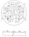
- FIG. 1is a schematic illustration of a conventional SEG wafer illustrating a disparate distribution of SEG sites on the wafer;
- FIG. 2is a section view through 2 — 2 of FIG. 1 showing the effect of loading on the SEG device region thickness
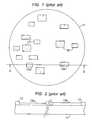
- FIG. 3is schematic illustration of a SEG wafer using the sea of SEG islands according to the invention.
- FIG. 4is a section through 4 — 4 of FIG. 3 illustrating the effect on the SEG device region thickness of using the sea of SEG islands according to the invention
- FIGS. 5-10are schematic representations of process steps useful for producing the wafer of the invention.
- a semiconductor wafer 11is shown with sites 12 where selective epitaxial growth (SEG) is performed.
- SEGselective epitaxial growth
- the typical waferwill have many more such sites of relatively smaller dimensions, and will have an orderly array of chip sites arranged in rows on the wafer.
- the chip sitesare usually identical and may constitute two or more SEG regions that exhibit the non-uniform thickness problem.
- the arrangement in FIG. 1more suitably shows the problem of nonuniform SEG layers across the wafer. Both are problems that are addressed by the invention.
- the disparate concentration of SEG sitesin either case will be qualitatively similar to that represented in FIG. 1 .
- FIG. 2is a section along section line 2 — 2 of FIG. 1 showing the relevant portions of the wafer where sites 12 a and 12 b are located.
- the field oxide 13is shown in this view around the perimeter of the SEG sites.
- the two sites 12 a and 12 bhave different epitaxial thickness as a result of the known loading effect on the growth process. Due to the close proximity of several other growth sites, the localized region above SEG site 12 a becomes relatively depleted of precursor gases as the process proceeds compared with the concentration of precursor gas over site 12 b . This causes a thickness variation in the epitaxial layers between the two sites.
- the waferis provided with a sea of passive SEG sites as shown in FIG. 3 .
- Passive sitesdesignated 31 in FIG. 3, are defined as regions where epitaxial layers are grown, but where no devices are located, i.e. regions devoid of electrical devices.
- the active SEG regionsare shown at 32 and are distributed unevenly as in FIG. 1 .
- the objectiveis to create a relatively even distribution of growth sites over the surface of the wafer.
- the effect of the passive sites, and the relatively even growth site distributionis to cause the precursor materials to distribute evenly over the wafer surface thereby reducing the loading effect and creating epitaxial layers of approximately equal thickness in each of the active SEG regions.
- the active device regionsare exaggerated in size for clarity.
- the passive regions in the figureare also shown as large areas. They are also shown as having a single area and shape. Both of these conditions can interfere with effective or optimum layout of the active circuits on the wafer. Consequently, the size of the passive regions can be made relatively small, and the shape and placement of these regions can be varied so that they have negligible or no impact on the design layout. As suggested by FIG. 3, it will usually be preferred that the passive sites be smaller in area than the active sites.
- FIGS. 5-10are schematic representations of process steps used for preparing SEG wafers with uniform growth regions for device manufacture. Two growth sites are illustrated, the site on the left hand site of the figures is an active site, and the site on the right hand side of the figures is a passive site. For illustration, the active site will contain an n-p-n vertical transistor. However, it will be understood that a variety of devices, including complementary pairs of bipolar and MOS transistors, may be formed on a single wafer.
- the bipolar transistorsmay be vertically or horizontally oriented, as known in the art.
- the MOS devicesmay be high voltage devices, or conventional MOS devices used for standard logic or memory. Other devices such as insulated gate bipolar (IGBT) devices may also be integrated in the wafers described here.
- IGBTinsulated gate bipolar
- wafer 51is a p-type wafer, preferably with (100) orientation and resistivity greater than 10 ohm cm.
- the waferis thermally oxidized in a conventional manner, e.g. furnace heating at 1000° C. in oxygen, to grow layer 52 .
- Layer 52may be approximately 0.5-2.0 microns in thickness.
- a photoresist mask layer 53is applied and patterned by conventional lithography to form openings, as shown in FIG. 6, over the active region 55 and the passive region 56 .
- the lithography usedwill normally be photolithography but other lithographic techniques such as e-beam or x-ray lithography may be substituted.
- the oxide layer 52is then patterned by standard etching, e.g. plasma or RIE etching, to produce the structure shown in FIG. 7, with openings down to substrate 51 .
- the exposed substrate regions at 55 and 56are implanted as shown in FIG. 8, to form the buried n+ collector region 58 .
- the passive site 56may masked against this implant but is preferably processed in the same way as site 55 so as to not add any process steps or process complexity in implementing the invention.
- the implanted regions 58may be formed using arsenic at 100 keV, with a dose in the range 5 ⁇ 10 14 to 5 ⁇ 10 15 atoms per cm 2 .
- the photoresist maskif present at this stage, is stripped.
- the implanted substratemay be annealed at this point, e.g. 1000° C. in nitrogen for 1 hour, to activate the implant and remove implant damage.
- Conventional chan stops or guard rings(not shown), normally used for isolation around the device regions, may be formed at this point by suitable masking and boron implants.
- epitaxial siliconis then selectively deposited in windows 55 and 56 to form SEG layers 59 over the buried n+ layers.
- a typical SEG deposition sequenceis:
- the SEG layers in the active regions, represented by region 55 , and the SEG layers in the passive regions, represented by region 56are uniform in thickness.
- the two epi regions 59are shown as comprising a single epitaxial deposit, i.e., the layers are formed in the same epitaxial deposition operation.
- the epitaxial layers in these two regionscan be formed using different depositions so as to result in different epitaxial materials at the two locations. Implicit is the presence of a plurality of regions of each composition, thus presenting the same problem/solution context described earlier.
- the SEG active regionsare then processed by conventional processing to form the desired active devices.
- An example of a vertical bipolar n-p-n deviceis shown in FIG. 10, where n+contact 61 is shown contacting the buried collector 58 .
- An oxide layeris grown or deposited over the SEG regions and standard masking and implantation are used to form the buried collector contact, and the base and emitter elements.
- P-type base layer 62 and P-contact regions 63are formed by conventional masking and boron implant.
- the n-type emitter region 64is implanted using an arsenic implant.
- the region 56is shown devoid of these active device features because the first oxide layer formed over all the SEG regions is not patterned but left intact over the passive regions.
- n+ contact region 61 that extends to the buried n+ collector region 58is shown to one side of SEG layer. It may be formed along a portion of the perimeter of the layer, as shown, or may extend around the whole layer. Suitable electrical contacts (not shown) are then made to the structure shown in FIG. 10 to complete the active device, and the device is then packaged in a conventional device package.
Landscapes
- Engineering & Computer Science (AREA)
- Physics & Mathematics (AREA)
- Condensed Matter Physics & Semiconductors (AREA)
- General Physics & Mathematics (AREA)
- Manufacturing & Machinery (AREA)
- Computer Hardware Design (AREA)
- Microelectronics & Electronic Packaging (AREA)
- Power Engineering (AREA)
- Chemical & Material Sciences (AREA)
- Crystallography & Structural Chemistry (AREA)
- Element Separation (AREA)
- Bipolar Transistors (AREA)
Abstract
Description
Claims (5)
Priority Applications (2)
| Application Number | Priority Date | Filing Date | Title |
|---|---|---|---|
| US10/091,291US6727567B2 (en) | 1999-12-15 | 2002-03-05 | Integrated circuit device substrates with selective epitaxial growth thickness compensation |
| DK03744218.3TDK1543117T3 (en) | 2002-03-05 | 2003-03-05 | High Capacity Mutagenesis Screening Method |
Applications Claiming Priority (2)
| Application Number | Priority Date | Filing Date | Title |
|---|---|---|---|
| US09/461,609US6409829B1 (en) | 1999-12-15 | 1999-12-15 | Manufacture of dielectrically isolated integrated circuits |
| US10/091,291US6727567B2 (en) | 1999-12-15 | 2002-03-05 | Integrated circuit device substrates with selective epitaxial growth thickness compensation |
Related Parent Applications (1)
| Application Number | Title | Priority Date | Filing Date |
|---|---|---|---|
| US09/461,609DivisionUS6409829B1 (en) | 1999-12-15 | 1999-12-15 | Manufacture of dielectrically isolated integrated circuits |
Publications (2)
| Publication Number | Publication Date |
|---|---|
| US20020092462A1 US20020092462A1 (en) | 2002-07-18 |
| US6727567B2true US6727567B2 (en) | 2004-04-27 |
Family
ID=23833259
Family Applications (2)
| Application Number | Title | Priority Date | Filing Date |
|---|---|---|---|
| US09/461,609Expired - LifetimeUS6409829B1 (en) | 1999-12-15 | 1999-12-15 | Manufacture of dielectrically isolated integrated circuits |
| US10/091,291Expired - LifetimeUS6727567B2 (en) | 1999-12-15 | 2002-03-05 | Integrated circuit device substrates with selective epitaxial growth thickness compensation |
Family Applications Before (1)
| Application Number | Title | Priority Date | Filing Date |
|---|---|---|---|
| US09/461,609Expired - LifetimeUS6409829B1 (en) | 1999-12-15 | 1999-12-15 | Manufacture of dielectrically isolated integrated circuits |
Country Status (1)
| Country | Link |
|---|---|
| US (2) | US6409829B1 (en) |
Cited By (7)
| Publication number | Priority date | Publication date | Assignee | Title |
|---|---|---|---|---|
| US20050104156A1 (en)* | 2003-11-13 | 2005-05-19 | Texas Instruments Incorporated | Forming a semiconductor structure in manufacturing a semiconductor device using one or more epitaxial growth processes |
| WO2005038861A3 (en)* | 2003-05-29 | 2005-10-20 | Paul N Marshall | High density integrated circuit package architecture |
| US20080166859A1 (en)* | 2007-01-05 | 2008-07-10 | Freescale Semiconductor, Inc. | Integrated assist features for epitaxial growth |
| US20110008951A1 (en)* | 2005-11-14 | 2011-01-13 | Taiwan Semiconductor Manufacturing Company, Ltd. | Method of manufacturing strained-silicon semiconductor device |
| US8508001B2 (en) | 2011-08-25 | 2013-08-13 | Globalfoundries Inc. | Semiconductor device with work function adjusting layer having varied thickness in a gate width direction and methods of making same |
| US20150115465A1 (en)* | 2013-10-29 | 2015-04-30 | Stats Chippac, Ltd. | Semiconductor Device and Method of Balancing Surfaces of an Embedded PCB Unit with a Dummy Copper Pattern |
| US11527642B2 (en)* | 2019-10-08 | 2022-12-13 | Samsung Electronics Co., Ltd. | Semiconductor device, method of fabricating the same, and display device including the same |
Families Citing this family (3)
| Publication number | Priority date | Publication date | Assignee | Title |
|---|---|---|---|---|
| US6837978B1 (en) | 1999-04-08 | 2005-01-04 | Applied Materials, Inc. | Deposition uniformity control for electroplating apparatus, and associated method |
| US20070111404A1 (en)* | 2005-11-14 | 2007-05-17 | Taiwan Semiconductor Manufacturing Company, Ltd. | Method of manufacturing strained-silicon semiconductor device |
| WO2010103792A1 (en)* | 2009-03-11 | 2010-09-16 | 住友化学株式会社 | Semiconductor substrate, method for manufacturing semiconductor substrate, electronic device and method for manufacturing electronic device |
Citations (7)
| Publication number | Priority date | Publication date | Assignee | Title |
|---|---|---|---|---|
| US4547231A (en)* | 1983-07-08 | 1985-10-15 | Mitsubishi Denki Kabushiki Kaisha | Method of manufacturing semiconductor device utilizing selective epitaxial growth under reduced pressure |
| US4698316A (en)* | 1985-01-23 | 1987-10-06 | Rca Corporation | Method of depositing uniformly thick selective epitaxial silicon |
| US4758531A (en)* | 1987-10-23 | 1988-07-19 | International Business Machines Corporation | Method of making defect free silicon islands using SEG |
| JPH01302838A (en)* | 1988-05-31 | 1989-12-06 | Nec Corp | Semiconductor device and its manufacture |
| US4923826A (en)* | 1989-08-02 | 1990-05-08 | Harris Corporation | Method for forming dielectrically isolated transistor |
| US6074478A (en)* | 1997-01-24 | 2000-06-13 | Nec Corporation | Method of facet free selective silicon epitaxy |
| US6232641B1 (en)* | 1998-05-29 | 2001-05-15 | Kabushiki Kaisha Toshiba | Semiconductor apparatus having elevated source and drain structure and manufacturing method therefor |
Family Cites Families (1)
| Publication number | Priority date | Publication date | Assignee | Title |
|---|---|---|---|---|
| US5773350A (en)* | 1997-01-28 | 1998-06-30 | National Semiconductor Corporation | Method for forming a self-aligned bipolar junction transistor with silicide extrinsic base contacts and selective epitaxial grown intrinsic base |
- 1999
- 1999-12-15USUS09/461,609patent/US6409829B1/ennot_activeExpired - Lifetime
- 2002
- 2002-03-05USUS10/091,291patent/US6727567B2/ennot_activeExpired - Lifetime
Patent Citations (7)
| Publication number | Priority date | Publication date | Assignee | Title |
|---|---|---|---|---|
| US4547231A (en)* | 1983-07-08 | 1985-10-15 | Mitsubishi Denki Kabushiki Kaisha | Method of manufacturing semiconductor device utilizing selective epitaxial growth under reduced pressure |
| US4698316A (en)* | 1985-01-23 | 1987-10-06 | Rca Corporation | Method of depositing uniformly thick selective epitaxial silicon |
| US4758531A (en)* | 1987-10-23 | 1988-07-19 | International Business Machines Corporation | Method of making defect free silicon islands using SEG |
| JPH01302838A (en)* | 1988-05-31 | 1989-12-06 | Nec Corp | Semiconductor device and its manufacture |
| US4923826A (en)* | 1989-08-02 | 1990-05-08 | Harris Corporation | Method for forming dielectrically isolated transistor |
| US6074478A (en)* | 1997-01-24 | 2000-06-13 | Nec Corporation | Method of facet free selective silicon epitaxy |
| US6232641B1 (en)* | 1998-05-29 | 2001-05-15 | Kabushiki Kaisha Toshiba | Semiconductor apparatus having elevated source and drain structure and manufacturing method therefor |
Non-Patent Citations (2)
| Title |
|---|
| Osenbach et al., A Complementary Selective Epitaxial Growth (CSEG) Process and its Application to High Speed Bipolar Transistors, 1990, IEEE, Custom Integrated Circuits Conference, pp. 18.4. 1-4.** |
| Sherman et al., Elimination of the Sidewall Defects in Selective Epitaxial Growth (SEG) of Silicon for a Dielectric Isolation Technology, Jun. 1996, IEEE, Electron Device Letters, vol. 17, No. 6, pp. 267-69.* |
Cited By (16)
| Publication number | Priority date | Publication date | Assignee | Title |
|---|---|---|---|---|
| WO2005038861A3 (en)* | 2003-05-29 | 2005-10-20 | Paul N Marshall | High density integrated circuit package architecture |
| US7030486B1 (en)* | 2003-05-29 | 2006-04-18 | Marshall Paul N | High density integrated circuit package architecture |
| US20060244097A1 (en)* | 2003-11-13 | 2006-11-02 | Wasshuber Christoph A | Forming a semiconductor structure in manufacturing a semiconductor device using one or more epitaxial growth processes |
| US7550343B2 (en) | 2003-11-13 | 2009-06-23 | Texas Instruments Incorporated | Forming a semiconductor structure in manufacturing a semiconductor device using one or more epitaxial growth processes |
| US20050104156A1 (en)* | 2003-11-13 | 2005-05-19 | Texas Instruments Incorporated | Forming a semiconductor structure in manufacturing a semiconductor device using one or more epitaxial growth processes |
| US20110008951A1 (en)* | 2005-11-14 | 2011-01-13 | Taiwan Semiconductor Manufacturing Company, Ltd. | Method of manufacturing strained-silicon semiconductor device |
| US8255843B2 (en) | 2005-11-14 | 2012-08-28 | Taiwan Semiconductor Manufacturing Company, Ltd. | Method of manufacturing strained-silicon semiconductor device |
| US8741743B2 (en)* | 2007-01-05 | 2014-06-03 | Freescale Semiconductor, Inc. | Integrated assist features for epitaxial growth |
| US20080166859A1 (en)* | 2007-01-05 | 2008-07-10 | Freescale Semiconductor, Inc. | Integrated assist features for epitaxial growth |
| US8508001B2 (en) | 2011-08-25 | 2013-08-13 | Globalfoundries Inc. | Semiconductor device with work function adjusting layer having varied thickness in a gate width direction and methods of making same |
| US20150115465A1 (en)* | 2013-10-29 | 2015-04-30 | Stats Chippac, Ltd. | Semiconductor Device and Method of Balancing Surfaces of an Embedded PCB Unit with a Dummy Copper Pattern |
| US9449943B2 (en)* | 2013-10-29 | 2016-09-20 | STATS ChipPAC Pte. Ltd. | Semiconductor device and method of balancing surfaces of an embedded PCB unit with a dummy copper pattern |
| US10177010B2 (en) | 2013-10-29 | 2019-01-08 | STATS ChipPAC Pte. Ltd. | Semiconductor device and method of balancing surfaces of an embedded PCB unit with a dummy copper pattern |
| US10790158B2 (en) | 2013-10-29 | 2020-09-29 | STATS ChipPAC Pte. Ltd. | Semiconductor device and method of balancing surfaces of an embedded PCB unit with a dummy copper pattern |
| US11527642B2 (en)* | 2019-10-08 | 2022-12-13 | Samsung Electronics Co., Ltd. | Semiconductor device, method of fabricating the same, and display device including the same |
| US12087853B2 (en)* | 2019-10-08 | 2024-09-10 | Samsung Electronics Co., Ltd. | Semiconductor device, method of fabricating the same, and display device including the same |
Also Published As
| Publication number | Publication date |
|---|---|
| US6409829B1 (en) | 2002-06-25 |
| US20020092462A1 (en) | 2002-07-18 |
Similar Documents
| Publication | Publication Date | Title |
|---|---|---|
| US4589193A (en) | Metal silicide channel stoppers for integrated circuits and method for making the same | |
| KR0163402B1 (en) | Merged bipolar/cmos technology using electrically active trench | |
| US5034338A (en) | Circuit containing integrated bipolar and complementary MOS transistors on a common substrate | |
| US7514337B2 (en) | Semiconductor device using EPI-layer and method of forming the same | |
| EP0137906A1 (en) | Method for fabricating vertical NPN and lateral PNP transistors in the same semiconductor body | |
| US7772100B2 (en) | Method of manufacturing a semiconductor device having a buried doped region | |
| EP0143662A2 (en) | Soi type semiconductor device | |
| US6727567B2 (en) | Integrated circuit device substrates with selective epitaxial growth thickness compensation | |
| KR100798158B1 (en) | Semiconductor device manufacturing method | |
| JP3078436B2 (en) | Method for forming a Bi-CMOS structure and Bi-CMOS structure | |
| US5641691A (en) | Method for fabricating complementary vertical bipolar junction transistors in silicon-on-sapphire | |
| US4081896A (en) | Method of making a substrate contact for an integrated circuit | |
| JP3372176B2 (en) | Semiconductor device and manufacturing method thereof | |
| US3981072A (en) | Bipolar transistor construction method | |
| US5837553A (en) | Method of making high voltage, junction isolation semiconductor device having dual conductivity type buried regions | |
| EP0206445A2 (en) | Process for forming a semiconductor cell in a silicon semiconductor body and a mixed CMOS/bipolar integrated circuit formed in a plurality of such cells | |
| US6774455B2 (en) | Semiconductor device with a collector contact in a depressed well-region | |
| US6740562B2 (en) | Manufacturing method of a semiconductor device having a polysilicon electrode | |
| US4056414A (en) | Process for producing an improved dielectrically-isolated silicon crystal utilizing adjacent areas of different insulators | |
| US6806159B2 (en) | Method for manufacturing a semiconductor device with sinker contact region | |
| US9018681B2 (en) | Method of manufacturing a bipolar transistor and bipolar transistor | |
| US12363926B2 (en) | Vertical deep trench and deep trench island based deep n-type well diode and diode triggered protection device | |
| US4814290A (en) | Method for providing increased dopant concentration in selected regions of semiconductor devices | |
| JPS58200554A (en) | Manufacturing method of semiconductor device | |
| ES2209523T3 (en) | METHOD FOR GENERATING A POLYCRYSTALLINE LAYER OR AMORFA ON AN INSULATING AREA. |
Legal Events
| Date | Code | Title | Description |
|---|---|---|---|
| STCF | Information on status: patent grant | Free format text:PATENTED CASE | |
| FPAY | Fee payment | Year of fee payment:4 | |
| FPAY | Fee payment | Year of fee payment:8 | |
| AS | Assignment | Owner name:DEUTSCHE BANK AG NEW YORK BRANCH, AS COLLATERAL AG Free format text:PATENT SECURITY AGREEMENT;ASSIGNORS:LSI CORPORATION;AGERE SYSTEMS LLC;REEL/FRAME:032856/0031 Effective date:20140506 | |
| AS | Assignment | Owner name:AVAGO TECHNOLOGIES GENERAL IP (SINGAPORE) PTE. LTD Free format text:ASSIGNMENT OF ASSIGNORS INTEREST;ASSIGNOR:AGERE SYSTEMS LLC;REEL/FRAME:035365/0634 Effective date:20140804 | |
| FPAY | Fee payment | Year of fee payment:12 | |
| AS | Assignment | Owner name:AGERE SYSTEMS LLC, PENNSYLVANIA Free format text:TERMINATION AND RELEASE OF SECURITY INTEREST IN PATENT RIGHTS (RELEASES RF 032856-0031);ASSIGNOR:DEUTSCHE BANK AG NEW YORK BRANCH, AS COLLATERAL AGENT;REEL/FRAME:037684/0039 Effective date:20160201 Owner name:LSI CORPORATION, CALIFORNIA Free format text:TERMINATION AND RELEASE OF SECURITY INTEREST IN PATENT RIGHTS (RELEASES RF 032856-0031);ASSIGNOR:DEUTSCHE BANK AG NEW YORK BRANCH, AS COLLATERAL AGENT;REEL/FRAME:037684/0039 Effective date:20160201 | |
| AS | Assignment | Owner name:BANK OF AMERICA, N.A., AS COLLATERAL AGENT, NORTH CAROLINA Free format text:PATENT SECURITY AGREEMENT;ASSIGNOR:AVAGO TECHNOLOGIES GENERAL IP (SINGAPORE) PTE. LTD.;REEL/FRAME:037808/0001 Effective date:20160201 Owner name:BANK OF AMERICA, N.A., AS COLLATERAL AGENT, NORTH Free format text:PATENT SECURITY AGREEMENT;ASSIGNOR:AVAGO TECHNOLOGIES GENERAL IP (SINGAPORE) PTE. LTD.;REEL/FRAME:037808/0001 Effective date:20160201 | |
| AS | Assignment | Owner name:AVAGO TECHNOLOGIES GENERAL IP (SINGAPORE) PTE. LTD., SINGAPORE Free format text:TERMINATION AND RELEASE OF SECURITY INTEREST IN PATENTS;ASSIGNOR:BANK OF AMERICA, N.A., AS COLLATERAL AGENT;REEL/FRAME:041710/0001 Effective date:20170119 Owner name:AVAGO TECHNOLOGIES GENERAL IP (SINGAPORE) PTE. LTD Free format text:TERMINATION AND RELEASE OF SECURITY INTEREST IN PATENTS;ASSIGNOR:BANK OF AMERICA, N.A., AS COLLATERAL AGENT;REEL/FRAME:041710/0001 Effective date:20170119 | |
| AS | Assignment | Owner name:BELL SEMICONDUCTOR, LLC, ILLINOIS Free format text:ASSIGNMENT OF ASSIGNORS INTEREST;ASSIGNORS:AVAGO TECHNOLOGIES GENERAL IP (SINGAPORE) PTE. LTD.;BROADCOM CORPORATION;REEL/FRAME:044886/0608 Effective date:20171208 Owner name:BELL SEMICONDUCTOR, LLC, ILLINOIS Free format text:ASSIGNMENT OF ASSIGNORS INTEREST;ASSIGNORS:AVAGO TECHNOLOGIES GENERAL IP (SINGAPORE) PTE. LTD.;BROADCOM CORPORATION;REEL/FRAME:044886/0766 Effective date:20171208 | |
| AS | Assignment | Owner name:CORTLAND CAPITAL MARKET SERVICES LLC, AS COLLATERA Free format text:SECURITY INTEREST;ASSIGNORS:HILCO PATENT ACQUISITION 56, LLC;BELL SEMICONDUCTOR, LLC;BELL NORTHERN RESEARCH, LLC;REEL/FRAME:045216/0020 Effective date:20180124 | |
| AS | Assignment | Owner name:BELL NORTHERN RESEARCH, LLC, ILLINOIS Free format text:RELEASE BY SECURED PARTY;ASSIGNOR:CORTLAND CAPITAL MARKET SERVICES LLC;REEL/FRAME:059723/0382 Effective date:20220401 Owner name:BELL SEMICONDUCTOR, LLC, ILLINOIS Free format text:RELEASE BY SECURED PARTY;ASSIGNOR:CORTLAND CAPITAL MARKET SERVICES LLC;REEL/FRAME:059723/0382 Effective date:20220401 Owner name:HILCO PATENT ACQUISITION 56, LLC, ILLINOIS Free format text:RELEASE BY SECURED PARTY;ASSIGNOR:CORTLAND CAPITAL MARKET SERVICES LLC;REEL/FRAME:059723/0382 Effective date:20220401 Owner name:BELL NORTHERN RESEARCH, LLC, ILLINOIS Free format text:RELEASE BY SECURED PARTY;ASSIGNOR:CORTLAND CAPITAL MARKET SERVICES LLC;REEL/FRAME:059720/0719 Effective date:20220401 Owner name:BELL SEMICONDUCTOR, LLC, ILLINOIS Free format text:RELEASE BY SECURED PARTY;ASSIGNOR:CORTLAND CAPITAL MARKET SERVICES LLC;REEL/FRAME:059720/0719 Effective date:20220401 Owner name:HILCO PATENT ACQUISITION 56, LLC, ILLINOIS Free format text:RELEASE BY SECURED PARTY;ASSIGNOR:CORTLAND CAPITAL MARKET SERVICES LLC;REEL/FRAME:059720/0719 Effective date:20220401 |