US6727520B2 - Spatially modulated reflector for an optoelectronic device - Google Patents
Spatially modulated reflector for an optoelectronic deviceDownload PDFInfo
- Publication number
- US6727520B2 US6727520B2US09/751,423US75142300AUS6727520B2US 6727520 B2US6727520 B2US 6727520B2US 75142300 AUS75142300 AUS 75142300AUS 6727520 B2US6727520 B2US 6727520B2
- Authority
- US
- United States
- Prior art keywords
- layer
- resonant reflector
- refractive index
- patterned regions
- optoelectronic device
- Prior art date
- Legal status (The legal status is an assumption and is not a legal conclusion. Google has not performed a legal analysis and makes no representation as to the accuracy of the status listed.)
- Expired - Fee Related, expires
Links
Images


Classifications
- H—ELECTRICITY
- H01—ELECTRIC ELEMENTS
- H01S—DEVICES USING THE PROCESS OF LIGHT AMPLIFICATION BY STIMULATED EMISSION OF RADIATION [LASER] TO AMPLIFY OR GENERATE LIGHT; DEVICES USING STIMULATED EMISSION OF ELECTROMAGNETIC RADIATION IN WAVE RANGES OTHER THAN OPTICAL
- H01S5/00—Semiconductor lasers
- H01S5/10—Construction or shape of the optical resonator, e.g. extended or external cavity, coupled cavities, bent-guide, varying width, thickness or composition of the active region
- H01S5/18—Surface-emitting [SE] lasers, e.g. having both horizontal and vertical cavities
- H01S5/183—Surface-emitting [SE] lasers, e.g. having both horizontal and vertical cavities having only vertical cavities, e.g. vertical cavity surface-emitting lasers [VCSEL]
- H01S5/18386—Details of the emission surface for influencing the near- or far-field, e.g. a grating on the surface
- H01S5/18388—Lenses
- H—ELECTRICITY
- H01—ELECTRIC ELEMENTS
- H01S—DEVICES USING THE PROCESS OF LIGHT AMPLIFICATION BY STIMULATED EMISSION OF RADIATION [LASER] TO AMPLIFY OR GENERATE LIGHT; DEVICES USING STIMULATED EMISSION OF ELECTROMAGNETIC RADIATION IN WAVE RANGES OTHER THAN OPTICAL
- H01S5/00—Semiconductor lasers
- H01S5/10—Construction or shape of the optical resonator, e.g. extended or external cavity, coupled cavities, bent-guide, varying width, thickness or composition of the active region
- H01S5/18—Surface-emitting [SE] lasers, e.g. having both horizontal and vertical cavities
- H01S5/183—Surface-emitting [SE] lasers, e.g. having both horizontal and vertical cavities having only vertical cavities, e.g. vertical cavity surface-emitting lasers [VCSEL]
- H01S5/18308—Surface-emitting [SE] lasers, e.g. having both horizontal and vertical cavities having only vertical cavities, e.g. vertical cavity surface-emitting lasers [VCSEL] having a special structure for lateral current or light confinement
- H—ELECTRICITY
- H01—ELECTRIC ELEMENTS
- H01S—DEVICES USING THE PROCESS OF LIGHT AMPLIFICATION BY STIMULATED EMISSION OF RADIATION [LASER] TO AMPLIFY OR GENERATE LIGHT; DEVICES USING STIMULATED EMISSION OF ELECTROMAGNETIC RADIATION IN WAVE RANGES OTHER THAN OPTICAL
- H01S2301/00—Functional characteristics
- H01S2301/16—Semiconductor lasers with special structural design to influence the modes, e.g. specific multimode
- H01S2301/166—Single transverse or lateral mode
- H—ELECTRICITY
- H01—ELECTRIC ELEMENTS
- H01S—DEVICES USING THE PROCESS OF LIGHT AMPLIFICATION BY STIMULATED EMISSION OF RADIATION [LASER] TO AMPLIFY OR GENERATE LIGHT; DEVICES USING STIMULATED EMISSION OF ELECTROMAGNETIC RADIATION IN WAVE RANGES OTHER THAN OPTICAL
- H01S5/00—Semiconductor lasers
- H01S5/10—Construction or shape of the optical resonator, e.g. extended or external cavity, coupled cavities, bent-guide, varying width, thickness or composition of the active region
- H01S5/18—Surface-emitting [SE] lasers, e.g. having both horizontal and vertical cavities
- H01S5/183—Surface-emitting [SE] lasers, e.g. having both horizontal and vertical cavities having only vertical cavities, e.g. vertical cavity surface-emitting lasers [VCSEL]
- H01S5/18308—Surface-emitting [SE] lasers, e.g. having both horizontal and vertical cavities having only vertical cavities, e.g. vertical cavity surface-emitting lasers [VCSEL] having a special structure for lateral current or light confinement
- H01S5/18322—Position of the structure
- H01S5/18327—Structure being part of a DBR
- H—ELECTRICITY
- H01—ELECTRIC ELEMENTS
- H01S—DEVICES USING THE PROCESS OF LIGHT AMPLIFICATION BY STIMULATED EMISSION OF RADIATION [LASER] TO AMPLIFY OR GENERATE LIGHT; DEVICES USING STIMULATED EMISSION OF ELECTROMAGNETIC RADIATION IN WAVE RANGES OTHER THAN OPTICAL
- H01S5/00—Semiconductor lasers
- H01S5/10—Construction or shape of the optical resonator, e.g. extended or external cavity, coupled cavities, bent-guide, varying width, thickness or composition of the active region
- H01S5/18—Surface-emitting [SE] lasers, e.g. having both horizontal and vertical cavities
- H01S5/183—Surface-emitting [SE] lasers, e.g. having both horizontal and vertical cavities having only vertical cavities, e.g. vertical cavity surface-emitting lasers [VCSEL]
- H01S5/18358—Surface-emitting [SE] lasers, e.g. having both horizontal and vertical cavities having only vertical cavities, e.g. vertical cavity surface-emitting lasers [VCSEL] containing spacer layers to adjust the phase of the light wave in the cavity
- H—ELECTRICITY
- H01—ELECTRIC ELEMENTS
- H01S—DEVICES USING THE PROCESS OF LIGHT AMPLIFICATION BY STIMULATED EMISSION OF RADIATION [LASER] TO AMPLIFY OR GENERATE LIGHT; DEVICES USING STIMULATED EMISSION OF ELECTROMAGNETIC RADIATION IN WAVE RANGES OTHER THAN OPTICAL
- H01S5/00—Semiconductor lasers
- H01S5/10—Construction or shape of the optical resonator, e.g. extended or external cavity, coupled cavities, bent-guide, varying width, thickness or composition of the active region
- H01S5/18—Surface-emitting [SE] lasers, e.g. having both horizontal and vertical cavities
- H01S5/183—Surface-emitting [SE] lasers, e.g. having both horizontal and vertical cavities having only vertical cavities, e.g. vertical cavity surface-emitting lasers [VCSEL]
- H01S5/18361—Structure of the reflectors, e.g. hybrid mirrors
- H01S5/18369—Structure of the reflectors, e.g. hybrid mirrors based on dielectric materials
- H—ELECTRICITY
- H01—ELECTRIC ELEMENTS
- H01S—DEVICES USING THE PROCESS OF LIGHT AMPLIFICATION BY STIMULATED EMISSION OF RADIATION [LASER] TO AMPLIFY OR GENERATE LIGHT; DEVICES USING STIMULATED EMISSION OF ELECTROMAGNETIC RADIATION IN WAVE RANGES OTHER THAN OPTICAL
- H01S5/00—Semiconductor lasers
- H01S5/10—Construction or shape of the optical resonator, e.g. extended or external cavity, coupled cavities, bent-guide, varying width, thickness or composition of the active region
- H01S5/18—Surface-emitting [SE] lasers, e.g. having both horizontal and vertical cavities
- H01S5/183—Surface-emitting [SE] lasers, e.g. having both horizontal and vertical cavities having only vertical cavities, e.g. vertical cavity surface-emitting lasers [VCSEL]
- H01S5/18361—Structure of the reflectors, e.g. hybrid mirrors
- H01S5/18377—Structure of the reflectors, e.g. hybrid mirrors comprising layers of different kind of materials, e.g. combinations of semiconducting with dielectric or metallic layers
- H—ELECTRICITY
- H01—ELECTRIC ELEMENTS
- H01S—DEVICES USING THE PROCESS OF LIGHT AMPLIFICATION BY STIMULATED EMISSION OF RADIATION [LASER] TO AMPLIFY OR GENERATE LIGHT; DEVICES USING STIMULATED EMISSION OF ELECTROMAGNETIC RADIATION IN WAVE RANGES OTHER THAN OPTICAL
- H01S5/00—Semiconductor lasers
- H01S5/10—Construction or shape of the optical resonator, e.g. extended or external cavity, coupled cavities, bent-guide, varying width, thickness or composition of the active region
- H01S5/18—Surface-emitting [SE] lasers, e.g. having both horizontal and vertical cavities
- H01S5/183—Surface-emitting [SE] lasers, e.g. having both horizontal and vertical cavities having only vertical cavities, e.g. vertical cavity surface-emitting lasers [VCSEL]
- H01S5/18386—Details of the emission surface for influencing the near- or far-field, e.g. a grating on the surface
- H01S5/18391—Aperiodic structuring to influence the near- or far-field distribution
Definitions
- This inventionrelates to the field of optoelectronic devices, and more particularly to resonant reflectors for optoelectronic devices.
- CMOScomplementary metal-oxide-semiconductor
- CMOScomplementary metal-oxide-semiconductor
- a semiconductor laseris coupled to a semiconductor receiver (e.g., photodiode) through a fiber optic link or even free space.
- This configurationmay provide a high speed communication path.
- Lasers that have a single or reduced mode outputare particularly suitable for many of these applications because, among other things, they can provide a small spot size.
- a typical edge-emitting semiconductor laseris a double heterostructure with a narrow bandgap, high refractive index layer surrounded on opposed major surfaces by wide bandgap, low refractive index layers.
- the low bandgap layeris termed the “active layer”, and the bandgap and refractive index differences serve to confine both charge carriers and optical energy to the active layer or region.
- Opposite ends of the active layerhave mirror facets which form the laser cavity.
- the cladding layershave opposite conductivity types and when current is passed through the structure, electrons and holes combine in the active layer to generate light.
- VCSELvertical cavity surface emitting laser
- Vertical Cavity Surface Emitting Lasersoffer numerous performance and potential producibility advantages over conventional edge emitting lasers. These include many benefits associated with their geometry, such as amenability to one- and two-dimensional arrays, wafer-level qualification, and desirable beam characteristics, typically circularly-symmetric low-divergence beams.
- VCSELstypically have an active region with bulk or one or more quantum well layers.
- mirror stackswhich are typically formed by interleaved semiconductor layers having properties, such that each layer is typically a quarter wavelength thick at the wavelength (in the medium) of interest thereby forming the mirrors for the laser cavity.
- conductivity type regionson opposite sides of the active region, and the laser is typically turned on and off by varying the current through the active region.
- VCSELsHigh-yield, high performance VCSELs have been demonstrated, and exploited in commercialization. Top-surface-emitting AlGaAs-based VCSELs are producible in a manner analogous to semiconductor integrated circuits, and are amenable to low-cost high-volume manufacture and integration with existing electronics technology platforms. Moreover, VCSEL uniformity and reproducibility have been demonstrated using a standard, unmodified commercially available metal organic vapor phase epitaxy (MOVPE) chamber and molecular beam epitaxy (MBE) giving very high device yields.
- MOVPEmetal organic vapor phase epitaxy
- MBEmolecular beam epitaxy
- VCSELsare expected to provide a performance and cost advantages in fast (e.g., Gbits/s) medium distance (e.g., up to approximately 1000 meters) single or multi-channel data link applications, and numerous optical and/or imaging applications. This results from their inherent geometry, which provides potential low-cost high performance transmitters with flexible and desirable characteristics.
- VCSELs of practical dimensionsare inherently multi (transverse) mode.
- Single lowest-order mode VCSELsare favored for coupling into single-mode fibers, and are advantageous for free-space and/or wavelength sensitive systems, and may even be beneficial for use in extending the bandwidth-length product of standard 50 ⁇ m and 62.5 ⁇ m GRIN multi-mode fiber.
- the short optical cavity (2 ⁇ ) of the VCSELfavors single longitudinal mode emission
- the multi-wavelength (110 ⁇ ) lateral dimensionsfacilitate multi-transverse mode operation.
- the present inventionovercomes many of the disadvantages of the prior art by providing a resonant reflector that increases mode control while not requiring a significant amount of additional processing steps. Some resonant reflectors of the present invention also reduce or eliminate abrupt changes in the reflectively across the resonant reflector. This may reduce undesirable diffraction effects that are common in many resonant reflectors, particularly those used for mode control of optoelectronic devices.
- a resonant reflectoris provided on top of a top mirror layer of an optoelectronic device.
- a first material layeris provided over the top mirror layer.
- the first material layeris then patterned, preferably by etching away the first material layer in the region or regions circumscribing the desired optical cavity of the optoelectronic device.
- a second material layeris then provided over the first material layer.
- the second material layeris preferably provided over both the etched and non-etched regions of the first material layer, but may only be provided over the non-etched regions, if desired.
- the top mirror layer of the optoelectronic devicemay function as the first material layer discussed above.
- the top mirror layermay be patterned, preferably by etching at least partially into the top mirror layer in the region or regions circumscribing the desired optical cavity of the optoelectronic device.
- the layer below the top mirror layermay function as an etch stop layer.
- a second material layeris provided over the top mirror layer. The second material layer is preferably provided over both the etched and non-etched regions of the top mirror layer, but may only be provided over the non-etched regions, if desired.
- the first material layer(or top mirror layer in an alternative embodiment) preferably has a refractive index that is less than the refractive index of the second material layer, and the first and second material layers preferably have a refractive index that is less than the refractive index of the top mirror layer (or next layer down in the alternative embodiment) of the optoelectroni device.
- Thiscauses a reduction in the reflectivity of the resonant reflector in those regions tha correspond to the etched regions of the first material layer (or top mirror layer).
- the differenc in reflectivitycan be used to provide mode control for optoelectronic devices.
- a resonant reflectoris formed by etching down but not all the way through one or more of the top mirror layers of an optoelectronic device.
- the etched regionpreferably circumscribes the desired optical cavity of the optoelectronic device, and has a depth that causes a phase shift that reduces the reflectivity of the resonant reflector at the desired operating wavelength, such as a depth that corresponds to an odd multiple of ⁇ /4.
- a cap mirror having one or more additional layersmay be provided on selected non-patterned regions of the top mirror layer, such as over the desired optical cavity of the optoelectronic device.
- a metal layermay be provided on selected patterned regions of the top mirror layer. The metal layer may function as a top contact layer.
- a resonant reflectorthat has a refractive index that does not change abruptly across the optical cavity of the optoelectronic device.
- the resonant reflectorhas at least one resonant reflector layer that has a refractive index that includes contributions from, for example, both a first material having a first refractive index and a second material having a second refractive index.
- the first materialis confined to a first region and the second material is confined to a second region, wherein the first region and the second region co-extend along an interface.
- the refractive index of the resonant reflector layerat least when viewed laterally along the optical cavity of the optoelectronic device, does not change abruptly across the optical cavity. Rather, there is a smooth transition from one refractive index to another. This may reduce the diffraction effects caused by abrupt changes in the refraction index of a resonant reflector.
- a number of methodsare contemplated for forming a resonant reflector layer that has a smooth transition from one refractive index to another.
- a first substantially planar layer of materialis provided and then patterned to form an island over the desired optical cavity.
- the islandis then heated, causing it to reflow. This results in an island of the first layer of material with a non-planar top surface.
- a second layer of materialis then provided over the first layer of material. Because the island of the first layer of material includes a non-planer top surface, and preferably one that tapers down, the second layer of material forms an interface with the first material layer that is non-parallel with the optical axis of the optoelectronic device. As indicated above, this may reduce the diffraction effects caused by abrupt changes in the refraction index of a resonant reflector.
- a first substantially planar layer of materialis provided, followed by a photoresist layer.
- the photoresist layeris then patterned, preferably forming an island of photoresist.
- the island of photoresistis then heated, causing it to reflow. This results in a non-planar top surface on the photoresist layer, and preferably one that tapers down toward the first layer of material.
- the photoresist layer and the first layer of materialare etched for a specified period of time. The etchant selectively etches both the photoresist layer and the first layer of material, thereby transferring the shape of the non-planar top surface of the photoresist layer to the first layer of material.
- a second layer of materialis then provided over the first layer of material, if desired. Because the first layer of material assumes the shape of the island of photoresist, and thus has a top surface that tapers down, the second layer of material forms an interface with the first material layer that is non-parallel with the optical axis of the optoelectronic device. As indicated above, this may reduce the diffraction effects caused by abrupt changes in the refraction index of a resonant reflector.
- a first substantially planar layer of materialis provided and patterned, resulting in an island of the first layer of material.
- the island of the first material layerpreferably has lateral surfaces that extend up to a top surface defined by top peripheral edges.
- a photoresist layeris then provided over the patterned first layer of material, including over the lateral surfaces, the top peripheral edges and the top surface. The step from the top surface down along the lateral surfaces causes the photoresist layer to be thinner near the top peripheral edges.
- the photoresist layer and the first layer of materialare then etched for a specified period of time. During this etch process, those regions of the first layer of material that are adjacent the thinner regions of the photoresist layer are subject to the etchant for a longer period of time than those regions that are adjacent thicker regions of the photoresist layer. Thus, in the illustrative embodiment, the top peripheral edges of the first layer of material are etched more than those regions away from the top peripheral edges. After the etch process, a second layer of material may be provided over the first layer of material.
- the top surface of the second layer of materialmay be planarized by heating the second layer of material to cause it to reflow.
- the top surface of the second layer of materialmay be planarized using a Chemical Mechanical Polishing (CMP) process.
- CMPChemical Mechanical Polishing
- the top surface of the second layer of materialmay remain substantially non-planar, if desired.
- FIG. 1is a schematic diagram of a planar, current-guided, GaAs/AlGaAs top surface emitting vertical cavity laser in accordance with the prior art
- FIG. 2is a schematic cross-sectional side view of a planar, current-guided, GaAs/AlGaAs top surface emitting vertical cavity laser with a first illustrative resonant reflector for increased mode control in accordance with the present invention
- FIGS. 3A-3Dare schematic cross-sectional side views showing an illustrative method for making the resonant reflector of FIG. 2;
- FIG. 4is a schematic cross-sectional side view of a planar, current-guided, GaAs/AlGaAs top surface emitting vertical cavity laser with a second illustrative resonant reflector for increased mode control in accordance with the present invention
- FIGS. 5A-5Dare schematic cross-sectional side views showing an illustrative method for making the resonant reflector of FIG. 4;
- FIG. 6is a schematic cross-sectional side view of a planar, current-guided, GaAs/AlGaAs top surface emitting vertical cavity laser with yet another illustrative resonant reflector for increased mode control in accordance with the present invention
- FIGS. 7A-7Dare schematic cross-sectional side views showing a first illustrative method for making the resonant reflector of FIG. 6;
- FIGS. 8A-8Eare schematic cross-sectional side views showing another illustrative method for making the resonant reflector of FIG. 6;
- FIGS. 9A-9Eare schematic cross-sectional side views showing yet another illustrative method for making the resonant reflector of FIG. 6;
- FIG. 10is a schematic cross-sectional side view showing another illustrative embodiment of the present invention similar to that shown in FIGS. 5A-5D;
- FIG. 11is a schematic cross-sectional side view showing another illustrative embodiment of the present invention similar to that shown in FIGS. 5A-5D;
- FIG. 12is a schematic cross-sectional side view showing another illustrative embodiment of the present invention similar to that shown in FIGS. 8 A- 8 E.
- FIG. 1is a schematic illustration of a planar, current-guided, GaAs/AlGaAs top surface emitting vertical cavity laser 10 in accordance with the prior art.
- n-doped gallium arsenide (GaAs) substrate 14is an n-contact 12 .
- Substrate 14is doped with impurities of a first type (i.e., n type).
- An n-type mirror stack 16is formed on substrate 14 .
- Spacer 18has a bottom confinement layer 20 and a top confinement layer 24 surrounding active region 22 .
- a p-type mirror stack 26is formed on top confinement layer 24 .
- a p-metal layer 28is formed on stack 26 .
- the emission regionmay have a passivation layer 30 .
- Isolation region 29restricts the area of the current flow 27 through the active region.
- Region 29may be formed by deep H+ ion implantation.
- the diameter “g”may be set to provide the desired active area, and thus the gain aperture of the VCSEL 10 . Further, the diameter “g” may be set by the desired resistance of the p-type mirror stack 26 , particularly through the non-conductive region 29 . Thus, non-conductive region 29 performs the gain guiding function.
- the diameter “g”is typically limited by fabrication limitations, such as lateral straggle during the implantation step.
- Spacer 18may contain a bulk or quantum-well active region disposed between mirror stacks 16 and 26 .
- Stacks 16 and 26are distributed Bragg reflector (DBR) stacks, and may include periodic layers of doped AlGaAs and aluminum arsenide (AlAs).
- DBRdistributed Bragg reflector
- the AlGaAs of stack 16is doped with the same type of impurity as substrate 14 (e.g., n type), and the AlGaAs of stack 26 is doped with the other kind of impurity (e.g., p type).
- Metal contact layers 12 and 28are ohmic contacts that allow appropriate electrical biasing of laser diode 10 .
- active region 22emits light 31 which passes through stack 26 .
- VCSELs of practical dimensionsare inherently multi (transverse) mode.
- Single lowest-order mode VCSELsare favored for coupling into single-mode fibers, and are advantageous for free-space and/or wavelength sensitive systems, and may even be beneficial for use in extending the bandwidth-length product of standard 50 ⁇ m and 62.5 ⁇ m GRIN multi-mode fiber.
- the short optical cavity (2 ⁇ ) of the VCSELfavors single longitudinal mode emission
- the multi-wavelength (10 ⁇ ) lateral dimensionsfacilitate multi-transverse mode operation.
- FIG. 2is a schematic cross-sectional side view of a planar, current-guided, GaAs/AlGaAs top surface emitting vertical cavity laser, as in FIG. 1, with a top mounted mode control resonant reflector 50 .
- the resonant reflector 50includes a patterned first material layer 56 that is positioned on top of the top mirror layer 52 of VCSEL 54 .
- a second material layer 58is provided over the patterned first material layer 56 , as shown.
- the first material layer 56preferably has a refractive index that is less than me refractive index of the second material layer 58 , and the first and second material layers 56 and 58 preferably have a refractive index that is less than the refractive index of the top mirror layer 52 of the optoelectronic device 54 .
- the first material layer 56is SiO 2
- the second material layer 58is Si 3 N 4 or TiO 2
- the top mirror layer 52is AlGaAs, although other suitable material systems are contemplated.
- Each layeris preferably an odd multiple of one-quarter wavelength ( ⁇ /4) thick. This causes a reduction in reflectivity of the resonant reflector 50 in those regions that correspond to the etched regions 60 (see FIG. 3B) in the first material layer 56 , that is, those regions that are filled with the second material layer 58 .
- this difference in reflectivitycan be used to help provide mode control for VCSEL 54 .
- the first material layer 56is provided over the top mirror layer 52 .
- the first material layer 56is patterned, preferably by etching away the first material layer 56 in the region or regions circumscribing the desired optical cavity of the VCSEL 54 .
- a second material layer 58is provided over the first material layer 56 .
- the second material layer 58is preferably provided over both the etched 60 and non-etched regions of the first material layer 56 , but may be confined to the non-etched regions if desired.
- Selected regionssuch as regions 62 a and 62 b of the second material layer 58 may then be removed to provide access to the top mirror layer 52 .
- a contact layer 64may be provided on the exposed regions of the top mirror layer 52 .
- the contact layer 64may provide electrical contact to the top mirror layer 52 .
- a top mirror layer of the optoelectronic devicemay function as the first material layer 56 discussed above.
- the top mirror layermay be patterned, preferably by etching at least partially into the top mirror layer in the region or regions circumscribing the desired optical cavity of the optoelectronic device.
- the layer 52 below the top mirror layermay function as an etch stop layer.
- a second material layer 58is provided over the top mirror layer.
- the second material layeris preferably provided over both the etched and non-etched regions of the top mirror layer, but may only be provided over the non-etched regions, if desired.
- the regions labeled 56 in FIGS. 2-3should have the same cross-hatch pattern as layer 53 , and the refractive index of these regions should be less than the refractive index of layer 52 .
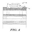
- FIG. 4is a schematic cross-sectional side view of a planar, current-guided, GaAs/AlGaAs top surface emitting vertical cavity laser, as in FIG. 1, with another illustrative top mounted mode control resonant reflector 70 .
- the resonant reflector 70is formed by etching down into but not all the way through one or more of the top mirror layers 72 of the optoelectronic device.
- the etched regionpreferably circumscribes the desired optical cavity of the optoelectronic device, and has a depth that causes a phase shift that reduces the reflectivity of the resonant reflector 70 at the desired operating wavelength, such as a depth that corresponds to an odd multiple of ⁇ /4.
- a cap mirror 76 having one or more additional layersmay be provided on selected non-patterned regions 78 of the top mirror layer 72 , such as over the desired optical cavity of the optoelectronic device.
- the cap mirror 76may include one or more periods of a conventional semiconductor DBR mirror, or more preferably, a narrow band dielectric reflection filter.
- a metal layermay be provided on selected regions of the top mirror layer 72 . The metal layer may function as a top contact layer.
- a top mirror layer 72(or some other top layer) is patterned and etched to form one or more etched regions 74 .
- the etched regions 74are preferably formed to circumscribe the desired optical cavity of the optoelectronic device. Also, the etched regions 74 are preferably etched down to a depth that causes a phase shift in the incident light, thereby reducing the reflectivity of the resonant reflector 70 in those regions.
- a cap mirror 76is formed on the patterned top mirror layer 72 .
- the top mirror layer 72may include one or more semiconductor DBR mirror periods, and/or a narrow band dielectric reflection filter. In either case, and to provide further differentiation in reflectivity, the cap mirror 76 may be etched away except on those areas that correspond to the desired optical cavity of the optoelectronic device. This is shown in FIG. 5 D.
- the patterned cap mirror 76may be formed using well known lift-off techniques.
- a contact layer 80may be provided on the selected regions of the top mirror layer 72 . The contact layer 80 may provide electrical contact to the top mirror layer 72 .
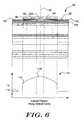
- FIG. 6is a schematic cross-sectional side view of a planar, current-guided, GaAs/AlGaAs top surface emitting vertical cavity laser, as in FIG. 1, with yet another illustrative top mounted mode control resonant reflector 90 .
- the resonant reflector 90has a refractive index that does not abruptly change across the optical cavity of the optoelectronic device.
- the resonant reflector 90has at least one resonant reflector layer 92 that has a refractive index.
- the refractive indexmay include, for example, contributions from both a first material 94 having a first refractive index and a second material 96 having a second refractive index.
- the first material 94is confined to a first region and the second material is confined to a second region, wherein the first region and the second region co-extend along an interface 98 .
- the refractive index of the resonant reflector layerdoes not change abruptly across the optical cavity. Rather, there is a smooth transition from one refractive index to another. This reduces the diffraction effects caused by abrupt changes in the refraction index. It is contemplated that one or more periods of a conventional semiconductor DBR mirror, or more preferably, a narrow band dielectric reflection filter 106 , may be provided on top of the resonant reflector 90 , as shown. Finally, a contact layer 102 may be provided around the periphery of the optical cavity. In the embodiment shown, the contact layer 102 is in direct contact with the top mirror layer 104 and provides electrical contact to the top mirror layer 104 .
- the smooth transition from one refractive index to anotheris further illustrated in chart 110 .
- the X axis of chart 110represents the lateral position along the optical cavity of the device shown above the chart.
- the Y axis of chart 110corresponds to the reflectivity “R” of the top mirror, including the resonant reflector 90 and conventional semiconductor DBR mirror or dielectric reflection filter 106 .
- the reflectivity “R” of the top mirror, at least in the region of the resonant reflector 90is dependent on the refractive index of the resonant reflector layer 90 .
- the reflectivitystarts at a first value 112 .
- the first value 112is shown relatively low because the resonant reflector 90 and the conventional semiconductor DBR mirror or dielectric reflection filter 106 do not extend out into this region.
- the contact layer 102may also decrease the reflectivity in this region.
- the reflectivityincreases to a value 114 , which includes contributions from the second material 96 of the resonant reflector layer 90 and the conventional semiconductor DBR mirror or dielectric reflection filter 106 .
- the refractive index of the resonant reflector 90begins to change due to the relative contributions of the first material 94 and the second material 96 . This causes the reflectivity of the resonant reflector 90 to smoothly increase toward the center of the desired optical cavity, as shown.
- the reflectivity of the resonant reflector 90reaches a maximum 116 in or around the center of the desired optical cavity.
- the reflectivity of the resonant reflector 90then decreases to the right of the center of the desired optical cavity, in an opposite manner to that described above.
- the refractive index, and thus the reflectivity, of the resonant reflector 90does not change abruptly across the optical cavity. Rather, there is a smooth transition from one refractive index to another. This reduces the diffraction effects often caused by abrupt changes in the refraction index of a resonant reflector.
- FIGS. 7A-7Dare schematic cross-sectional side views showing a first illustrative method for making the resonant reflector of FIG. 6 .
- a first substantially planar layer of material 94is provided on, for example, a top mirror layer 104 of a conventional DBR mirror.
- the top mirror layer 104preferably has a refractive index that is higher than the refractive index of the first layer of material 94 .
- the top mirror layer 104may be, for example, AlGaAs, and the first layer of material 94 may be, for example, SiO2, or a polymer such as polyamide or Benzocyclobuthene (BCB).
- the first layer of materialis then patterned, as shown in FIG. 7 A. This is typically done using a conventional etch process. As shown in FIG. 7B, the patterned first layer of material 104 is then heated, which causes it to reflow. This results in a non-planar top surface 98 . Then, and as shown in FIG. 7C, a second layer of material 96 is provided over the first layer of material 94 .
- the top surface 105 of the second layer of material 96is preferably substantially planar, but it may be non-planar if desired.
- the second layer of material 96preferably has a refractive index that is higher than the refractive index of the first layer of material 94 .
- the second layer of material 96may be, for example, TiO2, Si3N4, a polymer, or any other suitable material.
- the top surface 105 of the second layer of material 96may be planarized using any suitable method including, for example, reflowing the second layer of material 96 , mechanical, chemical or chemical-mechanical polishing (CMP) the second layer of material 96 etc.
- CMPchemical-mechanical polishing
- the to surface 105is left non-planar.
- the second layer of material 96is preferably provided over the entire top surface of the resonant reflector, and etched away in those regions where a top contact 102 is desired. Once the second layer of material 96 is etched, a contact layer 102 is provided on the exposed regions of the top mirror layer 104 . The contact layer 102 provides electrical contact to the top mirror layer 104 . As shown in FIG. 7D, a cap mirror 106 may then be provided above the second layer of material 96 .
- the cap mirror 106may include one or more periods of a conventional semiconductor DBR mirror, or more preferably, a narrow band dielectric reflection filter.
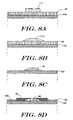
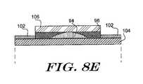
- FIGS. 8A-8Eare schematic cross-sectional side views showing another illustrative method for making the resonant reflector of FIG. 6 .
- a first substantially planar layer of material 94is provided on, for example, a top mirror layer 104 of a conventional DBR mirror.
- the top mirror layer 104preferably has a refractive index that is higher than the refractive index of the first layer of material 94 .
- the top mirror layer 104may be, for example, AlGaAs, and the first layer of material 94 may be, for example, SiO2, or any other suitable material.
- a photoresist layer 110is provided and patterned on the first layer of material 94 , preferably forming an island of photoresist above the desired optical cavity of the optoelectronic device.
- the photoresist layer 110is then heated, causing it to reflow. This results in a non-planar top surface on the photoresist layer 110 . That is, the top surface of the photoresist layer 110 may have portions that taper down toward the first layer of material 94 .
- the photoresist layer 110 and the first layer of material 94are etched for a specified period of time.
- the etchantpreferably selectively etches both the photoresist layer 110 and the first layer of material 94 . This transfers the shape of the non-planar top surface of the photoresist layer 110 to the first layer of material 94 .
- a second layer of material 96is then provided over the first layer of material 94 .
- the second layer of material 96preferably has a refractive index that is higher than the refractive index of the first layer of material 94 .
- the second layer of material 96is preferably provided over the entire top surface of the resonant reflector, and etched away in those regions where a top contact 102 is desired.
- a contact layer 102is provided on the exposed regions of the top mirror layer 104 .
- the contact layer 102provides electrical contact to the top mirror layer 104 .
- the top surface of the second layer of material 96is substantially planar.
- a cap mirror 106may be provided above the second layer of material 96 , if desired.
- the cap mirror 106may include one or more periods of a conventional semiconductor DBR mirror, or more preferably, a narrow band dielectric reflection filter.
- FIGS. 9A-9Eare schematic cross-sectional side views showing yet another illustrative method for making the resonant reflector of FIG. 6 .
- a first substantially planar layer of material 94is provided on, for example, a top mirror layer 104 of a conventional DBR mirror.
- the top mirror layer 104preferably has a refractive index that is higher than the refractive index of the first layer of material 94 .
- the first layer of material 94is patterned, preferably forming an island above the desired optical cavity of the optoelectronic device. This results in the first layer of material 94 having lateral surfaces 118 that extend up to a top surface 116 that is defined by top peripheral edges 120 .
- a photoresist layer 114is then provided over the patterned first layer of material 94 , including over the lateral surfaces 118 , the top peripheral edges 120 and the top surface 116 . Because of the step between the top surface 116 and the lateral surfaces 118 , the photoresist layer 114 is thinner near the top peripheral edges 120 than along either the lateral surfaces 118 or top surface 116 of the patterned first layer of material 94 , as shown.
- the photoresist layer 114 and the first layer of material 94are then etched for a specified period of time. During this etch step, those regions of the first layer of material 94 that are adjacent the thinner regions of the photoresist layer 114 are subject to the etchant for a longer period of time than those regions that are adjacent thicker regions of the photoresist layer 114 . Thus, and as shown in FIG. 9C, the top peripheral edges 120 of the first layer of material 94 are etched more than those regions away from the top peripheral edges 120 , resulting in tapered edges 122 .
- a second layer of material 96may be provided over the first layer of material 94 .
- the second layer of material 96preferably has a refractive index that is higher than the refractive index of the first layer of material 94 .
- the second layer of material 96is preferably provided over the entire top surface of the resonant reflector, and etched away in those regions where a top contact 102 is desired.
- a contact layer 102is provided on the exposed regions of the top mirror layer 104 .
- the contact layer 102provides electrical contact to the top mirror layer 104 .
- the top surface of the second layer of material 96is substantially planar.
- a cap mirror 106may be provided above the second layer of material 96 , if desired.
- the cap mirror 106may include one or more periods of a conventional semiconductor DBR mirror, or more preferably, a narrow band dielectric reflection filter.
- FIG. 10is a schematic cross-sectional side view showing another illustrative embodiment of the present invention similar to that shown in FIGS. 5A-5D.
- a top layer 110which may be the top mirror layer of the top DBR mirror stack of the optoelectronic device or an additional layer on top of the top mirror layer, may be etched down—but not all the way through.
- the etched regionpreferably circumscribes the desired optical cavity of the optoelectronic device, and has a depth that causes a phase shift that reduces the reflectivity of the resonant reflector at the desired operating wavelength, such as a depth that corresponds to an odd multiple of ⁇ /4.
- a cap mirror 112 having one or more additional layersmay be provided on selected non-patterned regions of layer 110 , such as over the desired optical cavity of the optoelectronic device, to provide further differentiation in reflectivity.
- a metal layer 114may then be provided on the etched region of layer 110 . The metal layer may function as the top contact.
- FIG. 11is a schematic cross-sectional side view showing another illustrative embodiment of the present invention similar to that shown in FIGS. 5A-5D. This embodiment is similar to that of FIG. 10, but the metal layer, now labeled 116 , extends over the etched region of layer 110 and over the cap mirror 112 . For back illumination devices, this may provide even better current spreading for the optoelectronic device.
- FIG. 12is a schematic cross-sectional side view showing another illustrative embodiment of the present invention similar to that shown in FIGS. 8A-8E.
- a resonant reflectoris provided that has a refractive index that does not change abruptly across the optical cavity of the optoelectronic device.
- the illustrative resonant reflectorincludes at least one resonant reflector layer that has a refractive index that includes contributions from, for example, both a first material 120 having a first refractive index and a second material 122 having a second refractive index.
- the first material 120is confined to a first region and the second material 122 is confined to a second region, wherein the first region and the second region co-extend along an interface.
- a metal layer 124is then provided over the entire structure.
- the metal layer 124may provide enhanced current spreading when compared to the device shown in FIGS. 8A-8E.
Landscapes
- Physics & Mathematics (AREA)
- Condensed Matter Physics & Semiconductors (AREA)
- General Physics & Mathematics (AREA)
- Electromagnetism (AREA)
- Optics & Photonics (AREA)
- Semiconductor Lasers (AREA)
- Aerials With Secondary Devices (AREA)
Abstract
Description
Claims (25)
Priority Applications (13)
| Application Number | Priority Date | Filing Date | Title |
|---|---|---|---|
| US09/751,423US6727520B2 (en) | 2000-12-29 | 2000-12-29 | Spatially modulated reflector for an optoelectronic device |
| EP01994427AEP1352455B1 (en) | 2000-12-29 | 2001-12-20 | Spatially modulated reflector for an optoelectronic device |
| DE60118974TDE60118974T2 (en) | 2000-12-29 | 2001-12-20 | SPATIALLY MODULATED REFLECTOR FOR AN OPTOELECTRONIC DEVICE |
| KR10-2003-7008908AKR20040018249A (en) | 2000-12-29 | 2001-12-20 | Spatially modulated reflector for an optoelectronic device |
| AT01994427TATE323959T1 (en) | 2000-12-29 | 2001-12-20 | SPACIALLY MODULATED REFLECTOR FOR AN OPTOELECTRONIC DEVICE |
| AU2002246819AAU2002246819A1 (en) | 2000-12-29 | 2001-12-20 | Spatially modulated reflector for an optoelectronic device |
| PCT/US2001/050214WO2002059938A2 (en) | 2000-12-29 | 2001-12-20 | Spatially modulated reflector for an optoelectronic device |
| CA002433357ACA2433357A1 (en) | 2000-12-29 | 2001-12-20 | Spatially modulated reflector for an optoelectronic device |
| JP2002560170AJP2004523896A (en) | 2000-12-29 | 2001-12-20 | Spatial modulated reflector for optoelectronic devices |
| TW090132789ATW517417B (en) | 2000-12-29 | 2001-12-28 | Spatially modulated reflector for an optoelectronic device |
| US10/819,654US7266135B2 (en) | 2000-12-29 | 2004-04-07 | Method for producing laser with resonant reflector |
| US10/819,775US20040188695A1 (en) | 2000-12-29 | 2004-04-07 | Laser with resonant reflector |
| US11/776,504US7760786B2 (en) | 2000-12-29 | 2007-07-19 | Laser with resonant reflector |
Applications Claiming Priority (1)
| Application Number | Priority Date | Filing Date | Title |
|---|---|---|---|
| US09/751,423US6727520B2 (en) | 2000-12-29 | 2000-12-29 | Spatially modulated reflector for an optoelectronic device |
Related Child Applications (2)
| Application Number | Title | Priority Date | Filing Date |
|---|---|---|---|
| US10/819,654DivisionUS7266135B2 (en) | 2000-12-29 | 2004-04-07 | Method for producing laser with resonant reflector |
| US10/819,775ContinuationUS20040188695A1 (en) | 2000-12-29 | 2004-04-07 | Laser with resonant reflector |
Publications (2)
| Publication Number | Publication Date |
|---|---|
| US20020085610A1 US20020085610A1 (en) | 2002-07-04 |
| US6727520B2true US6727520B2 (en) | 2004-04-27 |
Family
ID=25021913
Family Applications (4)
| Application Number | Title | Priority Date | Filing Date |
|---|---|---|---|
| US09/751,423Expired - Fee RelatedUS6727520B2 (en) | 2000-12-29 | 2000-12-29 | Spatially modulated reflector for an optoelectronic device |
| US10/819,775AbandonedUS20040188695A1 (en) | 2000-12-29 | 2004-04-07 | Laser with resonant reflector |
| US10/819,654Expired - Fee RelatedUS7266135B2 (en) | 2000-12-29 | 2004-04-07 | Method for producing laser with resonant reflector |
| US11/776,504Expired - LifetimeUS7760786B2 (en) | 2000-12-29 | 2007-07-19 | Laser with resonant reflector |
Family Applications After (3)
| Application Number | Title | Priority Date | Filing Date |
|---|---|---|---|
| US10/819,775AbandonedUS20040188695A1 (en) | 2000-12-29 | 2004-04-07 | Laser with resonant reflector |
| US10/819,654Expired - Fee RelatedUS7266135B2 (en) | 2000-12-29 | 2004-04-07 | Method for producing laser with resonant reflector |
| US11/776,504Expired - LifetimeUS7760786B2 (en) | 2000-12-29 | 2007-07-19 | Laser with resonant reflector |
Country Status (10)
| Country | Link |
|---|---|
| US (4) | US6727520B2 (en) |
| EP (1) | EP1352455B1 (en) |
| JP (1) | JP2004523896A (en) |
| KR (1) | KR20040018249A (en) |
| AT (1) | ATE323959T1 (en) |
| AU (1) | AU2002246819A1 (en) |
| CA (1) | CA2433357A1 (en) |
| DE (1) | DE60118974T2 (en) |
| TW (1) | TW517417B (en) |
| WO (1) | WO2002059938A2 (en) |
Cited By (13)
| Publication number | Priority date | Publication date | Assignee | Title |
|---|---|---|---|---|
| US20040188695A1 (en)* | 2000-12-29 | 2004-09-30 | Morgan Robert A. | Laser with resonant reflector |
| US20060045162A1 (en)* | 2004-08-31 | 2006-03-02 | Finisar Corporation | Distributed bragg reflector for optoelectronic device |
| US20060045146A1 (en)* | 2004-08-31 | 2006-03-02 | Finisar Corporation | Mode selective semiconductor mirror for vertical cavity surface emitting lasers |
| US20060268954A1 (en)* | 2004-08-31 | 2006-11-30 | Johnson Ralph H | Light emitting semiconductor device having an electrical confinement barrier near the active region |
| US20070014324A1 (en)* | 2005-07-04 | 2007-01-18 | Osamu Maeda | Vertical cavity surface emitting laser |
| US20070133641A1 (en)* | 2005-12-13 | 2007-06-14 | Seiko Epson Corporation | Surface-emitting type semiconductor laser and method for manufacturing the same |
| US20080023688A1 (en)* | 2006-07-31 | 2008-01-31 | Finisar Corporation | Efficient carrier injection in a semiconductor device |
| US20090180506A1 (en)* | 2008-01-10 | 2009-07-16 | Sony Corporation | Vertical cavity surface emitting laser |
| US8031752B1 (en) | 2007-04-16 | 2011-10-04 | Finisar Corporation | VCSEL optimized for high speed data |
| CN102545039A (en)* | 2010-12-10 | 2012-07-04 | 佳能株式会社 | Surface emitting laser |
| WO2015124531A3 (en)* | 2014-02-24 | 2015-10-15 | Osram Opto Semiconductors Gmbh | Laser diode chip having coated laser facet |
| USRE48577E1 (en)* | 2008-01-10 | 2021-06-01 | Sony Corporation | Vertical cavity surface emitting laser |
| US11476378B2 (en)* | 2019-05-03 | 2022-10-18 | University Of Central Florida Research Foundation, Inc. | Solar-energy apparatus, methods, and applications |
Families Citing this family (18)
| Publication number | Priority date | Publication date | Assignee | Title |
|---|---|---|---|---|
| KR100475858B1 (en)* | 2002-04-01 | 2005-03-18 | 주식회사 테라스테이트 | A Vertical Cavity Surface Emitting Lasers |
| TW200505120A (en)* | 2003-07-29 | 2005-02-01 | Copax Photonics Corp | Single transverse mode vertical cavity surface emitting laser device with array structure and method for fabricating the same |
| JP2007109737A (en)* | 2005-10-11 | 2007-04-26 | Toshiba Corp | Nitride semiconductor laser device and manufacturing method thereof |
| US7883914B2 (en)* | 2006-05-29 | 2011-02-08 | Alight Technologies A/S | Method for fabricating a photonic crystal or photonic bandgap vertical-cavity surface-emitting laser |
| WO2011046244A1 (en)* | 2009-10-16 | 2011-04-21 | 서울대학교산학협력단 | Iii-nitride surface grating reflector |
| DE102009056387B9 (en)* | 2009-10-30 | 2020-05-07 | Osram Opto Semiconductors Gmbh | Edge-emitting semiconductor laser with a phase structure area for the selection of lateral laser modes |
| JP5532239B2 (en)* | 2009-11-26 | 2014-06-25 | 株式会社リコー | Surface emitting laser element, surface emitting laser array, optical scanning device, and image forming apparatus |
| EP2533380B8 (en)* | 2011-06-06 | 2017-08-30 | Mellanox Technologies, Ltd. | High speed lasing device |
| JP2015008271A (en)* | 2013-05-31 | 2015-01-15 | 株式会社リコー | Surface emitting laser element and atomic oscillator |
| CN104297825B (en)* | 2014-10-17 | 2017-04-05 | 中国科学院上海光学精密机械研究所 | Light laser vortex reflecting mirror |
| US9979158B1 (en)* | 2017-01-12 | 2018-05-22 | Technische Universitaet Berlin | Vertical-cavity surface-emitting laser |
| FR3078834B1 (en)* | 2018-03-08 | 2020-03-27 | Commissariat A L'energie Atomique Et Aux Energies Alternatives | LIGHT EMITTING DEVICE COMPRISING AT LEAST ONE VCSEL AND A DIFFUSION LENS |
| JP7258591B2 (en)* | 2019-02-21 | 2023-04-17 | スタンレー電気株式会社 | Vertical cavity light emitting device |
| US11209398B2 (en)* | 2019-09-13 | 2021-12-28 | Applied Materials, Inc. | High quality factor embedded resonator wafers |
| WO2021150304A1 (en)* | 2020-01-23 | 2021-07-29 | Yale University | Stacked high contrast gratings and methods of making and using thereof |
| WO2021167666A1 (en)* | 2020-01-23 | 2021-08-26 | Yale University | Control and localization of porosity in iii-nitrides and methods of using and making thereof |
| US20220385041A1 (en)* | 2021-05-27 | 2022-12-01 | Lumentum Operations Llc | Emitter with variable light reflectivity |
| US12088064B2 (en) | 2021-08-05 | 2024-09-10 | Ii-Vi Delaware, Inc. | Reflector for VCSEL |
Citations (71)
| Publication number | Priority date | Publication date | Assignee | Title |
|---|---|---|---|---|
| US4317085A (en) | 1979-09-12 | 1982-02-23 | Xerox Corporation | Channeled mesa laser |
| US4466694A (en) | 1978-06-15 | 1984-08-21 | Her Majesty The Queen In Right Of Canada, As Represented By The Minister Of National Defence Of Her Majesty's Canadian Government | Wavelength selective optical coupler |
| JPS60123084A (en) | 1983-12-08 | 1985-07-01 | Matsushita Electric Ind Co Ltd | semiconductor light generator |
| US4660207A (en) | 1984-11-21 | 1987-04-21 | Northern Telecom Limited | Surface-emitting light emitting device |
| EP0288184A2 (en) | 1987-04-21 | 1988-10-26 | Gec-Marconi Limited | Semiconductor diode laser array |
| US4784722A (en) | 1985-01-22 | 1988-11-15 | Massachusetts Institute Of Technology | Method forming surface emitting diode laser |
| US4885592A (en) | 1987-12-28 | 1989-12-05 | Kofol J Stephen | Electronically steerable antenna |
| US4901327A (en) | 1988-10-24 | 1990-02-13 | General Dynamics Corporation, Electronics Division | Transverse injection surface emitting laser |
| JPH0254981A (en) | 1988-08-20 | 1990-02-23 | Fujitsu Ltd | Surface emitting laser and laser array |
| US4943970A (en) | 1988-10-24 | 1990-07-24 | General Dynamics Corporation, Electronics Division | Surface emitting laser |
| US4956844A (en) | 1989-03-17 | 1990-09-11 | Massachusetts Institute Of Technology | Two-dimensional surface-emitting laser array |
| US5031187A (en) | 1990-02-14 | 1991-07-09 | Bell Communications Research, Inc. | Planar array of vertical-cavity, surface-emitting lasers |
| US5034958A (en) | 1990-04-19 | 1991-07-23 | Bell Communications Research, Inc. | Front-surface emitting diode laser |
| US5052016A (en) | 1990-05-18 | 1991-09-24 | University Of New Mexico | Resonant-periodic-gain distributed-feedback surface-emitting semiconductor laser |
| US5056098A (en) | 1990-07-05 | 1991-10-08 | At&T Bell Laboratories | Vertical cavity laser with mirror having controllable reflectivity |
| US5062115A (en) | 1990-12-28 | 1991-10-29 | Xerox Corporation | High density, independently addressable, surface emitting semiconductor laser/light emitting diode arrays |
| US5068869A (en) | 1987-06-19 | 1991-11-26 | Lockheed Missiles & Space Company, Inc. | Surface-emitting laser diode |
| US5115442A (en) | 1990-04-13 | 1992-05-19 | At&T Bell Laboratories | Top-emitting surface emitting laser structures |
| US5140605A (en) | 1991-06-27 | 1992-08-18 | Xerox Corporation | Thermally stabilized diode laser structure |
| US5158908A (en) | 1990-08-31 | 1992-10-27 | At&T Bell Laboratories | Distributed bragg reflectors and devices incorporating same |
| US5216263A (en) | 1990-11-29 | 1993-06-01 | Xerox Corporation | High density, independently addressable, surface emitting semiconductor laser-light emitting diode arrays |
| US5216680A (en) | 1991-07-11 | 1993-06-01 | Board Of Regents, The University Of Texas System | Optical guided-mode resonance filter |
| US5237581A (en) | 1990-11-14 | 1993-08-17 | Nec Corporation | Semiconductor multilayer reflector and light emitting device with the same |
| US5245622A (en) | 1992-05-07 | 1993-09-14 | Bandgap Technology Corporation | Vertical-cavity surface-emitting lasers with intra-cavity structures |
| US5258316A (en) | 1992-03-26 | 1993-11-02 | Motorola, Inc. | Patterened mirror vertical cavity surface emitting laser |
| US5258990A (en) | 1991-11-07 | 1993-11-02 | The United States Of America As Represented By The Secretary Of The United States Department Of Energy | Visible light surface emitting semiconductor laser |
| JPH05299779A (en) | 1992-04-22 | 1993-11-12 | Seiko Epson Corp | Surface light emitting type semiconductor laser |
| US5285466A (en) | 1992-05-20 | 1994-02-08 | Wisconsin Alumni Research Foundation | Feedback mechanism for vertical cavity surface emitting lasers |
| US5293392A (en) | 1992-07-31 | 1994-03-08 | Motorola, Inc. | Top emitting VCSEL with etch stop layer |
| US5317587A (en) | 1992-08-06 | 1994-05-31 | Motorola, Inc. | VCSEL with separate control of current distribution and optical mode |
| DE4240706A1 (en) | 1992-12-03 | 1994-06-09 | Siemens Ag | Surface emitting laser diode |
| US5325386A (en) | 1992-04-21 | 1994-06-28 | Bandgap Technology Corporation | Vertical-cavity surface emitting laser assay display system |
| US5331654A (en) | 1993-03-05 | 1994-07-19 | Photonics Research Incorporated | Polarized surface-emitting laser |
| US5349599A (en) | 1990-03-29 | 1994-09-20 | Larkins Eric C | Bistable optical laser based on a heterostructure PNPN thyristor |
| US5351256A (en) | 1993-04-28 | 1994-09-27 | The United States Of America As Represented By The United States Department Of Energy | Electrically injected visible vertical cavity surface emitting laser diodes |
| US5359618A (en) | 1993-06-01 | 1994-10-25 | Motorola, Inc. | High efficiency VCSEL and method of fabrication |
| US5359447A (en) | 1993-06-25 | 1994-10-25 | Hewlett-Packard Company | Optical communication with vertical-cavity surface-emitting laser operating in multiple transverse modes |
| US5363397A (en) | 1992-10-29 | 1994-11-08 | Internatioal Business Machines Corporation | Integrated short cavity laser with bragg mirrors |
| US5373520A (en) | 1992-08-12 | 1994-12-13 | Fujitsu Limited | Surface emitting laser and method of manufacturing the same |
| US5404373A (en) | 1991-11-08 | 1995-04-04 | University Of New Mexico | Electro-optical device |
| US5416044A (en) | 1993-03-12 | 1995-05-16 | Matsushita Electric Industrial Co., Ltd. | Method for producing a surface-emitting laser |
| US5428634A (en) | 1992-11-05 | 1995-06-27 | The United States Of America As Represented By The United States Department Of Energy | Visible light emitting vertical cavity surface emitting lasers |
| US5446754A (en) | 1993-11-05 | 1995-08-29 | Photonics Research Incorporated | Phased array semiconductor laser |
| US5475701A (en) | 1993-12-29 | 1995-12-12 | Honeywell Inc. | Integrated laser power monitor |
| US5513202A (en) | 1994-02-25 | 1996-04-30 | Matsushita Electric Industrial Co., Ltd. | Vertical-cavity surface-emitting semiconductor laser |
| EP0712182A2 (en) | 1994-11-14 | 1996-05-15 | Sharp Kabushiki Kaisha | Surface-emitting laser |
| US5530715A (en) | 1994-11-29 | 1996-06-25 | Motorola, Inc. | Vertical cavity surface emitting laser having continuous grading |
| US5557626A (en) | 1994-06-15 | 1996-09-17 | Motorola | Patterned mirror VCSEL with adjustable selective etch region |
| US5561683A (en) | 1994-01-27 | 1996-10-01 | Kwon; O'dae | Circular grating surface emitting laser diode |
| US5568499A (en) | 1995-04-07 | 1996-10-22 | Sandia Corporation | Optical device with low electrical and thermal resistance bragg reflectors |
| US5574738A (en) | 1995-06-07 | 1996-11-12 | Honeywell Inc. | Multi-gigahertz frequency-modulated vertical-cavity surface emitting laser |
| US5598300A (en) | 1995-06-05 | 1997-01-28 | Board Of Regents, The University Of Texas System | Efficient bandpass reflection and transmission filters with low sidebands based on guided-mode resonance effects |
| US5606572A (en) | 1994-03-24 | 1997-02-25 | Vixel Corporation | Integration of laser with photodiode for feedback control |
| EP0776076A1 (en) | 1995-11-21 | 1997-05-28 | Thomson-Csf | Optoelectronic quantum well device |
| US5727013A (en) | 1995-10-27 | 1998-03-10 | Wisconsin Alumni Research Foundation | Single lobe surface emitting complex coupled distributed feedback semiconductor laser |
| US5774487A (en) | 1996-10-16 | 1998-06-30 | Honeywell Inc. | Filamented multi-wavelength vertical-cavity surface emitting laser |
| US5778018A (en) | 1994-10-13 | 1998-07-07 | Nec Corporation | VCSELs (vertical-cavity surface emitting lasers) and VCSEL-based devices |
| US5838715A (en) | 1996-06-20 | 1998-11-17 | Hewlett-Packard Company | High intensity single-mode VCSELs |
| FR2768566A1 (en) | 1997-09-12 | 1999-03-19 | France Telecom | COMPONENTS WITH AN OPTICAL CAVITY DEFINED BY AT LEAST ONE CURVED MIRROR |
| US5903590A (en) | 1996-05-20 | 1999-05-11 | Sandia Corporation | Vertical-cavity surface-emitting laser device |
| WO1999031735A1 (en) | 1997-12-12 | 1999-06-24 | Honeywell, Inc. | Bandgap isolated light emitter |
| US5940422A (en)* | 1996-06-28 | 1999-08-17 | Honeywell Inc. | Laser with an improved mode control |
| US5978401A (en) | 1995-10-25 | 1999-11-02 | Honeywell Inc. | Monolithic vertical cavity surface emitting laser and resonant cavity photodetector transceiver |
| US6026111A (en) | 1997-10-28 | 2000-02-15 | Motorola, Inc. | Vertical cavity surface emitting laser device having an extended cavity |
| US6055262A (en) | 1997-06-11 | 2000-04-25 | Honeywell Inc. | Resonant reflector for improved optoelectronic device performance and enhanced applicability |
| US6078601A (en) | 1997-03-07 | 2000-06-20 | Smith; David F. | Method for controlling the operation of a laser |
| WO2000045483A1 (en) | 1999-01-29 | 2000-08-03 | University Of Sheffield | Optical device and method of manufacture |
| US6144682A (en) | 1998-10-29 | 2000-11-07 | Xerox Corporation | Spatial absorptive and phase shift filter layer to reduce modal reflectivity for higher order modes in a vertical cavity surface emitting laser |
| US6185241B1 (en) | 1998-10-29 | 2001-02-06 | Xerox Corporation | Metal spatial filter to enhance model reflectivity in a vertical cavity surface emitting laser |
| US6238944B1 (en) | 1999-12-21 | 2001-05-29 | Xerox Corporation | Buried heterostructure vertical-cavity surface-emitting laser diodes using impurity induced layer disordering (IILD) via a buried impurity source |
| US6411638B1 (en) | 1999-08-31 | 2002-06-25 | Honeywell Inc. | Coupled cavity anti-guided vertical-cavity surface-emitting laser |
Family Cites Families (20)
| Publication number | Priority date | Publication date | Assignee | Title |
|---|---|---|---|---|
| US4466094A (en)* | 1982-12-27 | 1984-08-14 | Gte Automatic Electric Inc. | Data capture arrangement for a conference circuit |
| JPS63126897A (en)* | 1986-05-02 | 1988-05-30 | Yoshitomi Pharmaceut Ind Ltd | Immunosuppressive factor |
| US5256680A (en)* | 1988-11-29 | 1993-10-26 | Warner-Lambert Company | 3,5-di-tertiary-butyl-4-hydroxyphenyl-1,3,4-thiadiazoles, and oxadiazoles and 3,5-di-tertiary-butyl-4-hydroxy-phenyl-1,2,4-thiadazoles, oxadiazoles and triazoles as antiinflammatory agents |
| JPH0675144B2 (en)* | 1989-01-12 | 1994-09-21 | 松下電器産業株式会社 | Optical modulation wave demodulator |
| US5253262A (en)* | 1990-10-31 | 1993-10-12 | Kabushiki Kaisha Toshiba | Semiconductor laser device with multi-directional reflector arranged therein |
| US5474701A (en)* | 1994-01-21 | 1995-12-12 | Buckman Laboratories International, Inc. | Enzymes for recreational water |
| JP3611593B2 (en)* | 1994-02-14 | 2005-01-19 | 日本オプネクスト株式会社 | Method for fabricating semiconductor optical device |
| GB2311166A (en)* | 1996-03-13 | 1997-09-17 | Sharp Kk | An optoelectronic semiconductor device |
| IL118209A0 (en)* | 1996-05-09 | 1998-02-08 | Yeda Res & Dev | Active electro-optical wavelength-selective mirrors and active electro-optic wavelength-selective filters |
| US5966399A (en)* | 1997-10-02 | 1999-10-12 | Motorola, Inc. | Vertical cavity surface emitting laser with integrated diffractive lens and method of fabrication |
| KR100273134B1 (en)* | 1997-11-29 | 2001-01-15 | 정선종 | Single-mode surface-emitting laser |
| US5979401A (en)* | 1998-08-10 | 1999-11-09 | Ford Global Technologies, Inc. | Internal combustion engine having induction system with aerodynamic charge motion control valve |
| JP2000330124A (en) | 1999-05-18 | 2000-11-30 | Canon Inc | Method of manufacturing electrode substrate and liquid crystal element |
| US6243517B1 (en)* | 1999-11-04 | 2001-06-05 | Sparkolor Corporation | Channel-switched cross-connect |
| US6778582B1 (en)* | 2000-03-06 | 2004-08-17 | Novalux, Inc. | Coupled cavity high power semiconductor laser |
| US6727520B2 (en)* | 2000-12-29 | 2004-04-27 | Honeywell International Inc. | Spatially modulated reflector for an optoelectronic device |
| US6782027B2 (en) | 2000-12-29 | 2004-08-24 | Finisar Corporation | Resonant reflector for use with optoelectronic devices |
| US6878958B2 (en)* | 2001-03-26 | 2005-04-12 | Gazillion Bits, Inc. | Vertical cavity surface emitting laser with buried dielectric distributed Bragg reflector |
| US6786601B1 (en)* | 2002-09-14 | 2004-09-07 | Shree Kumar Kurup | Method of conveniently thwarting infant amblyopia after cataract removal |
| DE102004022178B4 (en)* | 2004-05-05 | 2008-03-20 | Atmel Germany Gmbh | Method for producing a conductor track on a substrate and component with a conductor track produced in this way |
- 2000
- 2000-12-29USUS09/751,423patent/US6727520B2/ennot_activeExpired - Fee Related
- 2001
- 2001-12-20JPJP2002560170Apatent/JP2004523896A/enactivePending
- 2001-12-20CACA002433357Apatent/CA2433357A1/ennot_activeAbandoned
- 2001-12-20DEDE60118974Tpatent/DE60118974T2/ennot_activeExpired - Lifetime
- 2001-12-20WOPCT/US2001/050214patent/WO2002059938A2/ennot_activeApplication Discontinuation
- 2001-12-20AUAU2002246819Apatent/AU2002246819A1/ennot_activeAbandoned
- 2001-12-20EPEP01994427Apatent/EP1352455B1/ennot_activeExpired - Lifetime
- 2001-12-20KRKR10-2003-7008908Apatent/KR20040018249A/ennot_activeCeased
- 2001-12-20ATAT01994427Tpatent/ATE323959T1/ennot_activeIP Right Cessation
- 2001-12-28TWTW090132789Apatent/TW517417B/ennot_activeIP Right Cessation
- 2004
- 2004-04-07USUS10/819,775patent/US20040188695A1/ennot_activeAbandoned
- 2004-04-07USUS10/819,654patent/US7266135B2/ennot_activeExpired - Fee Related
- 2007
- 2007-07-19USUS11/776,504patent/US7760786B2/ennot_activeExpired - Lifetime
Patent Citations (76)
| Publication number | Priority date | Publication date | Assignee | Title |
|---|---|---|---|---|
| US4466694A (en) | 1978-06-15 | 1984-08-21 | Her Majesty The Queen In Right Of Canada, As Represented By The Minister Of National Defence Of Her Majesty's Canadian Government | Wavelength selective optical coupler |
| US4317085A (en) | 1979-09-12 | 1982-02-23 | Xerox Corporation | Channeled mesa laser |
| JPS60123084A (en) | 1983-12-08 | 1985-07-01 | Matsushita Electric Ind Co Ltd | semiconductor light generator |
| US4660207A (en) | 1984-11-21 | 1987-04-21 | Northern Telecom Limited | Surface-emitting light emitting device |
| US4784722A (en) | 1985-01-22 | 1988-11-15 | Massachusetts Institute Of Technology | Method forming surface emitting diode laser |
| EP0288184A2 (en) | 1987-04-21 | 1988-10-26 | Gec-Marconi Limited | Semiconductor diode laser array |
| US5068869A (en) | 1987-06-19 | 1991-11-26 | Lockheed Missiles & Space Company, Inc. | Surface-emitting laser diode |
| US4885592A (en) | 1987-12-28 | 1989-12-05 | Kofol J Stephen | Electronically steerable antenna |
| JPH0254981A (en) | 1988-08-20 | 1990-02-23 | Fujitsu Ltd | Surface emitting laser and laser array |
| US4943970A (en) | 1988-10-24 | 1990-07-24 | General Dynamics Corporation, Electronics Division | Surface emitting laser |
| US4901327A (en) | 1988-10-24 | 1990-02-13 | General Dynamics Corporation, Electronics Division | Transverse injection surface emitting laser |
| US4956844A (en) | 1989-03-17 | 1990-09-11 | Massachusetts Institute Of Technology | Two-dimensional surface-emitting laser array |
| US5031187A (en) | 1990-02-14 | 1991-07-09 | Bell Communications Research, Inc. | Planar array of vertical-cavity, surface-emitting lasers |
| US5349599A (en) | 1990-03-29 | 1994-09-20 | Larkins Eric C | Bistable optical laser based on a heterostructure PNPN thyristor |
| US5115442A (en) | 1990-04-13 | 1992-05-19 | At&T Bell Laboratories | Top-emitting surface emitting laser structures |
| US5034958A (en) | 1990-04-19 | 1991-07-23 | Bell Communications Research, Inc. | Front-surface emitting diode laser |
| US5052016A (en) | 1990-05-18 | 1991-09-24 | University Of New Mexico | Resonant-periodic-gain distributed-feedback surface-emitting semiconductor laser |
| US5056098A (en) | 1990-07-05 | 1991-10-08 | At&T Bell Laboratories | Vertical cavity laser with mirror having controllable reflectivity |
| US5158908A (en) | 1990-08-31 | 1992-10-27 | At&T Bell Laboratories | Distributed bragg reflectors and devices incorporating same |
| US5237581A (en) | 1990-11-14 | 1993-08-17 | Nec Corporation | Semiconductor multilayer reflector and light emitting device with the same |
| US5317170A (en) | 1990-11-29 | 1994-05-31 | Xerox Corporation | High density, independently addressable, surface emitting semiconductor laser/light emitting diode arrays without a substrate |
| US5216263A (en) | 1990-11-29 | 1993-06-01 | Xerox Corporation | High density, independently addressable, surface emitting semiconductor laser-light emitting diode arrays |
| US5062115A (en) | 1990-12-28 | 1991-10-29 | Xerox Corporation | High density, independently addressable, surface emitting semiconductor laser/light emitting diode arrays |
| US5337074A (en) | 1990-12-28 | 1994-08-09 | Xerox Corporation | Opto-electronic line printer having a high density, independently addressable, surface emitting semiconductor laser/light emitting diode array |
| US5140605A (en) | 1991-06-27 | 1992-08-18 | Xerox Corporation | Thermally stabilized diode laser structure |
| US5216680A (en) | 1991-07-11 | 1993-06-01 | Board Of Regents, The University Of Texas System | Optical guided-mode resonance filter |
| US5642376A (en) | 1991-11-07 | 1997-06-24 | Vixel Corporation | Visible light surface emitting semiconductor laser |
| US5258990A (en) | 1991-11-07 | 1993-11-02 | The United States Of America As Represented By The Secretary Of The United States Department Of Energy | Visible light surface emitting semiconductor laser |
| US5404373A (en) | 1991-11-08 | 1995-04-04 | University Of New Mexico | Electro-optical device |
| US5258316A (en) | 1992-03-26 | 1993-11-02 | Motorola, Inc. | Patterened mirror vertical cavity surface emitting laser |
| US5325386A (en) | 1992-04-21 | 1994-06-28 | Bandgap Technology Corporation | Vertical-cavity surface emitting laser assay display system |
| JPH05299779A (en) | 1992-04-22 | 1993-11-12 | Seiko Epson Corp | Surface light emitting type semiconductor laser |
| US5245622A (en) | 1992-05-07 | 1993-09-14 | Bandgap Technology Corporation | Vertical-cavity surface-emitting lasers with intra-cavity structures |
| US5285466A (en) | 1992-05-20 | 1994-02-08 | Wisconsin Alumni Research Foundation | Feedback mechanism for vertical cavity surface emitting lasers |
| US5293392A (en) | 1992-07-31 | 1994-03-08 | Motorola, Inc. | Top emitting VCSEL with etch stop layer |
| US5317587A (en) | 1992-08-06 | 1994-05-31 | Motorola, Inc. | VCSEL with separate control of current distribution and optical mode |
| US5373520A (en) | 1992-08-12 | 1994-12-13 | Fujitsu Limited | Surface emitting laser and method of manufacturing the same |
| US5363397A (en) | 1992-10-29 | 1994-11-08 | Internatioal Business Machines Corporation | Integrated short cavity laser with bragg mirrors |
| US5428634A (en) | 1992-11-05 | 1995-06-27 | The United States Of America As Represented By The United States Department Of Energy | Visible light emitting vertical cavity surface emitting lasers |
| DE4240706A1 (en) | 1992-12-03 | 1994-06-09 | Siemens Ag | Surface emitting laser diode |
| US5555255A (en) | 1992-12-03 | 1996-09-10 | Siemens Aktiengesellschaft | Surface-emitting laser diode |
| US5331654A (en) | 1993-03-05 | 1994-07-19 | Photonics Research Incorporated | Polarized surface-emitting laser |
| US5416044A (en) | 1993-03-12 | 1995-05-16 | Matsushita Electric Industrial Co., Ltd. | Method for producing a surface-emitting laser |
| US5351256A (en) | 1993-04-28 | 1994-09-27 | The United States Of America As Represented By The United States Department Of Energy | Electrically injected visible vertical cavity surface emitting laser diodes |
| US5359618A (en) | 1993-06-01 | 1994-10-25 | Motorola, Inc. | High efficiency VCSEL and method of fabrication |
| US5359447A (en) | 1993-06-25 | 1994-10-25 | Hewlett-Packard Company | Optical communication with vertical-cavity surface-emitting laser operating in multiple transverse modes |
| US5446754A (en) | 1993-11-05 | 1995-08-29 | Photonics Research Incorporated | Phased array semiconductor laser |
| US5475701A (en) | 1993-12-29 | 1995-12-12 | Honeywell Inc. | Integrated laser power monitor |
| US5561683A (en) | 1994-01-27 | 1996-10-01 | Kwon; O'dae | Circular grating surface emitting laser diode |
| US5513202A (en) | 1994-02-25 | 1996-04-30 | Matsushita Electric Industrial Co., Ltd. | Vertical-cavity surface-emitting semiconductor laser |
| US5606572A (en) | 1994-03-24 | 1997-02-25 | Vixel Corporation | Integration of laser with photodiode for feedback control |
| US5557626A (en) | 1994-06-15 | 1996-09-17 | Motorola | Patterned mirror VCSEL with adjustable selective etch region |
| US5778018A (en) | 1994-10-13 | 1998-07-07 | Nec Corporation | VCSELs (vertical-cavity surface emitting lasers) and VCSEL-based devices |
| EP0712182A2 (en) | 1994-11-14 | 1996-05-15 | Sharp Kabushiki Kaisha | Surface-emitting laser |
| US5530715A (en) | 1994-11-29 | 1996-06-25 | Motorola, Inc. | Vertical cavity surface emitting laser having continuous grading |
| US5568499A (en) | 1995-04-07 | 1996-10-22 | Sandia Corporation | Optical device with low electrical and thermal resistance bragg reflectors |
| US5598300A (en) | 1995-06-05 | 1997-01-28 | Board Of Regents, The University Of Texas System | Efficient bandpass reflection and transmission filters with low sidebands based on guided-mode resonance effects |
| US5574738A (en) | 1995-06-07 | 1996-11-12 | Honeywell Inc. | Multi-gigahertz frequency-modulated vertical-cavity surface emitting laser |
| US5978401A (en) | 1995-10-25 | 1999-11-02 | Honeywell Inc. | Monolithic vertical cavity surface emitting laser and resonant cavity photodetector transceiver |
| US5727013A (en) | 1995-10-27 | 1998-03-10 | Wisconsin Alumni Research Foundation | Single lobe surface emitting complex coupled distributed feedback semiconductor laser |
| EP0776076A1 (en) | 1995-11-21 | 1997-05-28 | Thomson-Csf | Optoelectronic quantum well device |
| US5818066A (en) | 1995-11-21 | 1998-10-06 | Thomson-Csf | Optoelectronic quantum well device having an optical resonant cavity and sustaining inter subband transitions |
| US5903590A (en) | 1996-05-20 | 1999-05-11 | Sandia Corporation | Vertical-cavity surface-emitting laser device |
| US5838715A (en) | 1996-06-20 | 1998-11-17 | Hewlett-Packard Company | High intensity single-mode VCSELs |
| US5940422A (en)* | 1996-06-28 | 1999-08-17 | Honeywell Inc. | Laser with an improved mode control |
| US5774487A (en) | 1996-10-16 | 1998-06-30 | Honeywell Inc. | Filamented multi-wavelength vertical-cavity surface emitting laser |
| US6078601A (en) | 1997-03-07 | 2000-06-20 | Smith; David F. | Method for controlling the operation of a laser |
| US6055262A (en) | 1997-06-11 | 2000-04-25 | Honeywell Inc. | Resonant reflector for improved optoelectronic device performance and enhanced applicability |
| FR2768566A1 (en) | 1997-09-12 | 1999-03-19 | France Telecom | COMPONENTS WITH AN OPTICAL CAVITY DEFINED BY AT LEAST ONE CURVED MIRROR |
| US6026111A (en) | 1997-10-28 | 2000-02-15 | Motorola, Inc. | Vertical cavity surface emitting laser device having an extended cavity |
| WO1999031735A1 (en) | 1997-12-12 | 1999-06-24 | Honeywell, Inc. | Bandgap isolated light emitter |
| US6144682A (en) | 1998-10-29 | 2000-11-07 | Xerox Corporation | Spatial absorptive and phase shift filter layer to reduce modal reflectivity for higher order modes in a vertical cavity surface emitting laser |
| US6185241B1 (en) | 1998-10-29 | 2001-02-06 | Xerox Corporation | Metal spatial filter to enhance model reflectivity in a vertical cavity surface emitting laser |
| WO2000045483A1 (en) | 1999-01-29 | 2000-08-03 | University Of Sheffield | Optical device and method of manufacture |
| US6411638B1 (en) | 1999-08-31 | 2002-06-25 | Honeywell Inc. | Coupled cavity anti-guided vertical-cavity surface-emitting laser |
| US6238944B1 (en) | 1999-12-21 | 2001-05-29 | Xerox Corporation | Buried heterostructure vertical-cavity surface-emitting laser diodes using impurity induced layer disordering (IILD) via a buried impurity source |
Non-Patent Citations (58)
| Title |
|---|
| "Surface-Emitting Microlasers for Photonic Switching and Interchip Connections", Optical Engineering, 29, pp. 210-214, Mar. 1990. |
| Banwell et al., "VCSE Laser Transmitters for Parallel Data Links", IEEE Journal of Quantum Electronics, vol. 29, No. 2, Feb. 1993, pp. 635-644. |
| Catchmark et al., "High Temperature CW Operation of Vertical Cavity Top Surface-Emitting Lasers", CLEO 1993, p. 138. |
| Chemla et al., "Nonlinear Optical Properties of Semiconductor Quantum Wells", Optical Nonlinearities and Instabilities in Semiconductors, Academic Press, Inc., Copyright 1988, pp. 83-120. |
| Choa et al., "High-Speed Modulation of Vertical-Cavity Surface-Emitting Lasers", IEEE Photonics Technology Letter, vol. 3, No. 8, Aug. 1991, pp. 697-699. |
| Choquette et al., "Lithographically-Defined Gain Apertures Within Selectively Oxidized VCSELs", paper CtuL6, Conference on Lasers and Electro-Optics, San Francisco, California (2000). |
| Cox, J. A., et al., "Guided Mode Grating Resonant Filters for VCSEL Applications", Proceedings of the SPIE, The International Society for Optical Engineering, Diffractive and Holographic Device Technologies and Applications V, San Jose, California, Jan. 28-29, 1998, vol. 3291, pp. 70-71. |
| G. G. Ortiz, et al., "Monolithic Integration of In0.2 GA0.8As Vertical Cavity Surface-Emitting Lasers with Resonance-Enhanced Quantum Well Photodetectors", Electronics Letters, vol. 32, No. 13, Jun. 20, 1996, pp. 1205-1207. |
| G. Shtengel et al., "High-Speed Vertical-Cavity Surface-Emitting Lasers", Photon. Tech. Lett., vol. 5, No. 12, pp. 1359-1361 (Dec. 1993). |
| Graf, Rudolph, Modern Dictionary of Electronics, 6<th >ed., Indiana: Howard W. Sams & Company, 1984, p. 694. |
| Graf, Rudolph, Modern Dictionary of Electronics, 6th ed., Indiana: Howard W. Sams & Company, 1984, p. 694. |
| Guenter et al., "Reliability of Proton-Implanted VCSELs for Data Communications", Invited paper, SPIE, vol. 2683, OE LASE 96; Photonics West, Fabrication, Testing and Reliability of Semiconductor Lasers, (SPIE, Bellingham, WA, 1996). |
| Hibbs-Brenner et al., "Performance, Uniformity and Yield of 850nm VCELs Deposited by MOVPE", IEEE Phot. Tech. Lett., vol. 8, No. 1, pp. 7-9, Jan. 1996. |
| Hornak et al., "Low-Temperature (10K-300K) Characterization of MOVPE-Grown Vertical-Cavity Surface-Emitting Lasers", Photon. Tech. Lett., vol. 7, No. 10, pp. 1110-1112, Oct. 1995. |
| Huffaker et al., "Lasing Characteristics of Low Threshold Microcavity Layers Using Half-Wave Spacer Layers and Lateral Index Confinement", Appl. Phys. Lett., vol. 66, No. 14, pp. 1723-1725, Apr. 3, 1995. |
| International Search Report, dated Mar. 12, 2003, relative to PCT application No. PCT/US 01/50214, the foreign equivalent to the instant U.S. application 09/751,423. |
| Jewell et al., "Surface Emitting Microlasers for Photonic Switching & Intership Connections", Optical Engineering, vol. 29, No. 3, pp. 210-214, Mar. 1990. |
| Jewell et al., "Surface-Emitting Microlasers for Photonic Switching and Interchip Connections", Optical Engineering, vol. 29, No. 3, Mar. 1990, pp. 210-214. |
| Jiang et al., "High-Frequency Polarization Self-Modulation in Vertical-Cavity Surface-Emitting Lasers", Appl. Phys. Letters, vol. 63, No. 26, Dec. 27, 1993, pp. 2545-2547. |
| K.L. Lear et al., "Selectivity Oxidized Vertical Cavity Surface-Emitting Lasers with 50% Power Conversion Efficiency", Elec. Lett., vol. 31, No. 3 pp. 208-209, Feb. 2, 1995. |
| Kishino et al., "Resonant Cavity-Enhanced (RCE) Photodectors", IEEE Journal of Quantum Electronics, vol. 27, No. 8, pp. 2025-2034. |
| Kuchibhotla et al., "Low-Voltage High Gain Resonant Cavity Avalanche Photodiode", IEEE Phototonics Technology Letters, vol. 3, No. 4, pp. 354-356. |
| Lai et al., "Design of a Tunable GaAs/AlGaAs Multiple-Quantum-Well Resonant Cavity Photodector", IEEE Journal of Quantum Electronics, vol. 30, No. 1, pp. 108-114. |
| Lee et al., "Top-Surface Emitting GaAs Four-Quantum-Well Lasers Emitting at 0.85 mum", Electronics Letters, vol. 24, No. 11, May 24, 1990, pp. 710-711. |
| Lee et al., "Top-Surface Emitting GaAs Four-Quantum-Well Lasers Emitting at 0.85 μm", Electronics Letters, vol. 24, No. 11, May 24, 1990, pp. 710-711. |
| Lehman et al., "High Frequency Modulation Characteristics of Hybrid Dielectric/AlGaAs Mirror Singlemode VCSELs", Electronic Letters, vol. 31, No. 15, Jul. 20, 1995, pp. 1251-1252. |
| Magnusson, "Integration of Guided-Mode Resonance Filters and VCSELs", Electo-Optics Research Center, Department of Electrical Engineering, University of Texas at Arlington, May 6, 1997. |
| Martinsson et al., "Transverse Mode Selection in Large-Area Oxide-Confined Vertical-Cavity Surface Emitting Lasers Using a Shallow Surface Relief", IEEE Photon, Technol. Lett., 11(12), 1536-1538 (1999). |
| Miller et al., "Optical Bistability Due to Increasing Absorption", Optics Letters, vol. 9, No. 5, May 1984, pp. 162-164. |
| Morgan "High-Performance, Producible Vertical Cavity Lasers for Optical Interconnects", High Speed Electronics and Systems, vol. 5, No. 4, Dec. 1994, pp. 65-95. |
| Morgan et al., "200 C9 96-nm Wavelength Range, Continuous-Wave Lasing from Unbonded GaAs MOVPE-Grown Vertical Cavity Surface-Emitting Lasers", IEEE Photonics Technology Letters, vol. 7, No. 5, May 1995, pp. 441-443. |
| Morgan et al., "High-Power Coherently Coupled 8×8 Vertical Cavity Surface Emitting Laser Array", Appl. Phy Letters, vol. 61, No. 10, Sep. 7, 1992, pp. 1160-1162. |
| Morgan et al., "High-Power Coherently Coupled 8x8 Vertical Cavity Surface Emitting Laser Array", Appl. Phy Letters, vol. 61, No. 10, Sep. 7, 1992, pp. 1160-1162. |
| Morgan et al., "Hybrid Dielectric/AlGaAs Mirror Spatially Filtered Vertical Cavity Top-Surface Emitting Laser", Appl. Phys. Letters, vol. 66, No. 10, Mar. 6, 1995, pp. 1157-1159. |
| Morgan et al., "Hybrid Dielectric/AlGaAs Mirror Spatially-Filtered Vertical Top-Surface Emitting Laser", Appl. Phys. Lett., vol. 60, No. 8, pp. 921-923, Feb. 24, 1992. |
| Morgan et al., "Novel Hibrid-DBR Single-Mode Controlled GaAs Top-Emitting VCSEL with Record Low Voltage", 2 pages, dated prior to Dec. 29, 2000. |
| Morgan et al., "One Watt Vertical Cavity Surface Emitting Laser", Electron. Lett., vol. 29, No. 2, pp. 206-207, Jan. 21, 1993. |
| Morgan et al., "Producible GaAs-based MOVPE-Grown Vertival-Cavity Top-Surface Emitting Lasers wth Record Performance", Elec. Lett., vol. 31, No. 6, pp. 462-464, Mar. 16, 1995. |
| Morgan et al., "Progress and Properties of High-Power Coherent Vertical Cavity Surface Emitting Laser Arrays", SPIE, Vo. 1850, Jan. 1993, pp. 100-108. |
| Morgan et al., "Progress in Planarized Vertical Cavity Surface Emitting Laser Devices and Arrays", SPIE, vol. 1562, Jul. 1991, pp. 149-159. |
| Morgan et al., "Spatial-Filtered Vertical-Cavity Top Surface-Emitting Lasers", CLEO, 1993, pp. 138-139. |
| Morgan et al., "Submilliamp Low-Resistance, Continuous-Wave, Single-Mode GaAs Planar Vertical-Cavity Surface Emitting Lasers", Honeywell Technology Center, Jun. 6, 1995. |
| Morgan et al., "Transverse Mode Control of Vertical-Cavity Top-Surface Emitting Lasers", IEEE Photonics Technology Letters, vol. 4, No. 4, Apr. 1993, pp. 374-377. |
| Morgan et al., "Vertical Cavity Surface Emitting Laser Arrays: Come of Age," , Invited paper, SPIE, vol. 2683-04, OE LASE 96; Photonics West: Frabrication, Testing and Relablity of Semiconductor Lasers, (SPIE>Bellingham, WA, 1996). |
| Morgan et al., "Vertical Cavity Surface Emitting Laser Arrays: Come of Age," , Invited paper, SPIE, vol. 2683-04, OE LASE 96; Photonics West: Frabrication, Testing and Reliablity of Semiconductor Lasers, (SPIE<Bellingham, WA, 1996). |
| Morgan et al., "Vertical-Cavity Surface-Emitting Laser Arrays" SPIE, vol. 2398, Feb. 1995, pp. 65-93. |
| Morgan, "Transverse Mode Control of Vertical-Cavity Top-Surface Emitting Lasers", IEEE Phot. Tech. Lett., vol. 4, No. 4., p. 374, Apr. 1993. |
| Nugent et al., "Self-Pulsations in Vertical-Cavity Surface-Emitting Lasers", Electronic Letters, vol. 31, No. 1, Jan. 5, 1995, pp. 43-44. |
| Oh, T. H. et al., "Single-Mode Operation in Antiguided Vertical-Cavity Surface-Emitting Laser Using a Low-Temperature Grown AlGaAs Dielectric Aperture", IEEE Photon. Technol. Lett, 10(8), 1064-1066 (1998). |
| S.S. Wang and R. Magnusson, "Multilayer Waveguide-Grating Filters", Appl. Opt., vol. 34, No. 14, pp. 2414-2420, 1995. |
| S.S. Wang and R. Magnusson, "Theory and Applications of Guided-Mode Resonance Filters", Appl. Opt., vol. 32, No. 14, pp. 2606-2613, 1993. |
| Schubert, "Resonant Cavity Light-Emitting Diode", Appl. Phys. Lett., vol. 60, No. 8, pp. 921-923, Feb. 24, 1992. |
| Smith, R.E. et al., Polarization-Sensitive Subwavelength Antireflection Surfaces on a Semiconductor for 975 NM, Optics Letters, vol. 21, No. 15, Aug. 1, 1996, pp. 1201-1203. |
| Suning Tang et al., "Design Limitations of Highly Parallel Free-Space Optical Interconnects Based on Arrays of Vertical Cavity Surface-Emitting Laser Diodes, Microlenses, and Photodetectors", Journal of Lightwave Technology, vol. 12, No. 11, Nov. 1, 1994, pp. 1971-1975. |
| U.S. patent application Ser. No. 09/751,422, filed Dec. 29, 2000, entitled "Resonant Reflector for Use with Optoelectronic Devices". |
| Y. M. Yang et al., "Ultralow Threshold Current Vertical Cavity Surface Emitting Lasers Obtained with Selective Oxidation", Elect. Lett., vol. 31, No. 11, pp. 886-888, May 25, 1995. |
| Yablonovitch et al., "Photonic Bandgap Structures", J. Opt. Soc. Am. B., vol. 10, No. 2, pp. 283-295, Feb. 1993. |
| Young et al., "Enhanced Performance of Offset-Gain High Barrier Vertical-Cavity Surface-Emitting Lasers", IEEE J. Wuantum Electron., vol. 29, No. 6, pp. 2013-2022, Jun. 1993. |
Cited By (27)
| Publication number | Priority date | Publication date | Assignee | Title |
|---|---|---|---|---|
| US7760786B2 (en) | 2000-12-29 | 2010-07-20 | Finisar Corporation | Laser with resonant reflector |
| US20040191941A1 (en)* | 2000-12-29 | 2004-09-30 | Morgan Robert A. | Method for producing laser with resonant reflector |
| US20040188695A1 (en)* | 2000-12-29 | 2004-09-30 | Morgan Robert A. | Laser with resonant reflector |
| US7266135B2 (en) | 2000-12-29 | 2007-09-04 | Finisar Corporation | Method for producing laser with resonant reflector |
| US20060045162A1 (en)* | 2004-08-31 | 2006-03-02 | Finisar Corporation | Distributed bragg reflector for optoelectronic device |
| US20060045146A1 (en)* | 2004-08-31 | 2006-03-02 | Finisar Corporation | Mode selective semiconductor mirror for vertical cavity surface emitting lasers |
| US20060268954A1 (en)* | 2004-08-31 | 2006-11-30 | Johnson Ralph H | Light emitting semiconductor device having an electrical confinement barrier near the active region |
| US7391799B2 (en) | 2004-08-31 | 2008-06-24 | Finisar Corporation | Mode selective semiconductor mirror for vertical cavity surface emitting lasers |
| US7920612B2 (en) | 2004-08-31 | 2011-04-05 | Finisar Corporation | Light emitting semiconductor device having an electrical confinement barrier near the active region |
| US7596165B2 (en) | 2004-08-31 | 2009-09-29 | Finisar Corporation | Distributed Bragg Reflector for optoelectronic device |
| US20070014324A1 (en)* | 2005-07-04 | 2007-01-18 | Osamu Maeda | Vertical cavity surface emitting laser |
| US8385381B2 (en)* | 2005-07-04 | 2013-02-26 | Sony Corporation | Vertical cavity surface emitting laser |
| US20070133641A1 (en)* | 2005-12-13 | 2007-06-14 | Seiko Epson Corporation | Surface-emitting type semiconductor laser and method for manufacturing the same |
| US20080023688A1 (en)* | 2006-07-31 | 2008-01-31 | Finisar Corporation | Efficient carrier injection in a semiconductor device |
| US7829912B2 (en) | 2006-07-31 | 2010-11-09 | Finisar Corporation | Efficient carrier injection in a semiconductor device |
| US8031752B1 (en) | 2007-04-16 | 2011-10-04 | Finisar Corporation | VCSEL optimized for high speed data |
| US8363687B2 (en) | 2008-01-10 | 2013-01-29 | Sony Corporation | Vertical cavity surface emitting laser |
| US8077752B2 (en)* | 2008-01-10 | 2011-12-13 | Sony Corporation | Vertical cavity surface emitting laser |
| US20110194579A1 (en)* | 2008-01-10 | 2011-08-11 | Sony Corporation | Vertical cavity surface emitting laser |
| US20090180506A1 (en)* | 2008-01-10 | 2009-07-16 | Sony Corporation | Vertical cavity surface emitting laser |
| USRE48577E1 (en)* | 2008-01-10 | 2021-06-01 | Sony Corporation | Vertical cavity surface emitting laser |
| CN102545039A (en)* | 2010-12-10 | 2012-07-04 | 佳能株式会社 | Surface emitting laser |
| CN102545039B (en)* | 2010-12-10 | 2014-09-03 | 佳能株式会社 | Surface emitting laser |
| US9046807B2 (en) | 2010-12-10 | 2015-06-02 | Canon Kabushiki Kaisha | Surface emitting laser |
| WO2015124531A3 (en)* | 2014-02-24 | 2015-10-15 | Osram Opto Semiconductors Gmbh | Laser diode chip having coated laser facet |
| US11695251B2 (en) | 2014-02-24 | 2023-07-04 | Osram Oled Gmbh | Laser diode chip having coated laser facet |
| US11476378B2 (en)* | 2019-05-03 | 2022-10-18 | University Of Central Florida Research Foundation, Inc. | Solar-energy apparatus, methods, and applications |
Also Published As
| Publication number | Publication date |
|---|---|
| AU2002246819A1 (en) | 2002-08-06 |
| US20040188695A1 (en) | 2004-09-30 |
| US20040191941A1 (en) | 2004-09-30 |
| US7760786B2 (en) | 2010-07-20 |
| WO2002059938A3 (en) | 2003-07-31 |
| US7266135B2 (en) | 2007-09-04 |
| KR20040018249A (en) | 2004-03-02 |
| ATE323959T1 (en) | 2006-05-15 |
| JP2004523896A (en) | 2004-08-05 |
| DE60118974T2 (en) | 2007-01-04 |
| EP1352455B1 (en) | 2006-04-19 |
| US20020085610A1 (en) | 2002-07-04 |
| TW517417B (en) | 2003-01-11 |
| WO2002059938A2 (en) | 2002-08-01 |
| EP1352455A2 (en) | 2003-10-15 |
| DE60118974D1 (en) | 2006-05-24 |
| CA2433357A1 (en) | 2002-08-01 |
| US20080037606A1 (en) | 2008-02-14 |
Similar Documents
| Publication | Publication Date | Title |
|---|---|---|
| US6727520B2 (en) | Spatially modulated reflector for an optoelectronic device | |
| US7288421B2 (en) | Method for forming an optoelectronic device having an isolation layer | |
| US6055262A (en) | Resonant reflector for improved optoelectronic device performance and enhanced applicability | |
| EP1208622B1 (en) | Coupled cavity anti-guided vertical cavity surface emitting laser (vcsel) | |
| US5903590A (en) | Vertical-cavity surface-emitting laser device | |
| US5812577A (en) | Surface-emitting laser | |
| TW202308247A (en) | Reflector for vcsel | |
| US7700941B2 (en) | Surface-emitting semiconductor laser comprising a structured waveguide | |
| US20060045162A1 (en) | Distributed bragg reflector for optoelectronic device | |
| CN112636172A (en) | Distributed oxide lens for beam shaping | |
| Unold et al. | Large-area single-mode selectively oxidized VCSELs: Approaches and experimental | |
| US7376163B2 (en) | Method for producing a waveguide structure in a surface-emitting semiconductor laser and surface-emitting semiconductor laser | |
| JP7522891B2 (en) | Vertical-cavity surface-emitting laser (VCSEL) emitter with guided-unguided waveguides - Patents.com | |
| HK1061609B (en) | Resonant reflector for use with optoelectronic devices |
Legal Events
| Date | Code | Title | Description |
|---|---|---|---|
| AS | Assignment | Owner name:HONEYWELL INTERNATIONAL INC., NEW JERSEY Free format text:ASSIGNMENT OF ASSIGNORS INTEREST;ASSIGNORS:MORGAN, ROBERT A.;STRZELECKI, EVA M.;REEL/FRAME:011723/0275;SIGNING DATES FROM 20010319 TO 20010328 | |
| AS | Assignment | Owner name:FINISAR CORPORATION, CALIFORNIA Free format text:ASSIGNMENT OF ASSIGNORS INTEREST;ASSIGNOR:HONEYWELL INTERNATIONAL, INC.;REEL/FRAME:014468/0371 Effective date:20040301 Owner name:FINISAR CORPORATION, CALIFORNIA Free format text:ASSIGNMENT OF ASSIGNORS INTEREST;ASSIGNOR:HONEYWELL INTERNATIONAL, INC.;REEL/FRAME:014468/0407 Effective date:20040301 Owner name:FINISAR CORPORATION, CALIFORNIA Free format text:ASSIGNMENT OF ASSIGNORS INTEREST;ASSIGNOR:HONEYWELL INTERNATIONAL, INC.;REEL/FRAME:014484/0171 Effective date:20040301 | |
| AS | Assignment | Owner name:FINISAR CORPORATION, CALIFORNIA Free format text:ASSIGNMENT OF ASSIGNORS INTEREST;ASSIGNOR:HONEYWELL INTERNATIONAL, INC.;REEL/FRAME:014499/0365 Effective date:20040301 | |
| CC | Certificate of correction | ||
| FPAY | Fee payment | Year of fee payment:4 | |
| REMI | Maintenance fee reminder mailed | ||
| FPAY | Fee payment | Year of fee payment:8 | |
| REMI | Maintenance fee reminder mailed | ||
| LAPS | Lapse for failure to pay maintenance fees | ||
| STCH | Information on status: patent discontinuation | Free format text:PATENT EXPIRED DUE TO NONPAYMENT OF MAINTENANCE FEES UNDER 37 CFR 1.362 | |
| FP | Lapsed due to failure to pay maintenance fee | Effective date:20160427 | |
| AS | Assignment | Owner name:II-VI DELAWARE, INC., DELAWARE Free format text:ASSIGNMENT OF ASSIGNORS INTEREST;ASSIGNOR:FINISAR CORPORATION;REEL/FRAME:052286/0001 Effective date:20190924 |