US6727474B2 - Rapid thermal processing chamber for processing multiple wafers - Google Patents
Rapid thermal processing chamber for processing multiple wafersDownload PDFInfo
- Publication number
- US6727474B2 US6727474B2US09/943,928US94392801AUS6727474B2US 6727474 B2US6727474 B2US 6727474B2US 94392801 AUS94392801 AUS 94392801AUS 6727474 B2US6727474 B2US 6727474B2
- Authority
- US
- United States
- Prior art keywords
- light energy
- wafers
- thermal processing
- energy sources
- processing chamber
- Prior art date
- Legal status (The legal status is an assumption and is not a legal conclusion. Google has not performed a legal analysis and makes no representation as to the accuracy of the status listed.)
- Expired - Fee Related
Links
Images


Classifications
- H—ELECTRICITY
- H01—ELECTRIC ELEMENTS
- H01L—SEMICONDUCTOR DEVICES NOT COVERED BY CLASS H10
- H01L21/00—Processes or apparatus adapted for the manufacture or treatment of semiconductor or solid state devices or of parts thereof
- H01L21/02—Manufacture or treatment of semiconductor devices or of parts thereof
- H01L21/04—Manufacture or treatment of semiconductor devices or of parts thereof the devices having potential barriers, e.g. a PN junction, depletion layer or carrier concentration layer
- H01L21/18—Manufacture or treatment of semiconductor devices or of parts thereof the devices having potential barriers, e.g. a PN junction, depletion layer or carrier concentration layer the devices having semiconductor bodies comprising elements of Group IV of the Periodic Table or AIIIBV compounds with or without impurities, e.g. doping materials
- H01L21/30—Treatment of semiconductor bodies using processes or apparatus not provided for in groups H01L21/20 - H01L21/26
- H01L21/324—Thermal treatment for modifying the properties of semiconductor bodies, e.g. annealing, sintering
- H—ELECTRICITY
- H01—ELECTRIC ELEMENTS
- H01L—SEMICONDUCTOR DEVICES NOT COVERED BY CLASS H10
- H01L21/00—Processes or apparatus adapted for the manufacture or treatment of semiconductor or solid state devices or of parts thereof
- H01L21/67—Apparatus specially adapted for handling semiconductor or electric solid state devices during manufacture or treatment thereof; Apparatus specially adapted for handling wafers during manufacture or treatment of semiconductor or electric solid state devices or components ; Apparatus not specifically provided for elsewhere
- H01L21/67005—Apparatus not specifically provided for elsewhere
- H01L21/67011—Apparatus for manufacture or treatment
- H01L21/67098—Apparatus for thermal treatment
- H01L21/67115—Apparatus for thermal treatment mainly by radiation
Definitions
- the present inventionis generally directed to rapid thermal processing chambers for heating semiconductor wafers using light energy. More particularly, the present invention is directed to rapid thermal processing chambers that are capable of processing a plurality of wafers at the same time.
- the firstis a batch system in which multiple wafers (25 wafers to about 200 wafers) are loaded into a round tubular furnace and slowly heated to the desired temperature.
- Batch systemscan be considered temperature equilibrium devices in that the furnace walls are approximately at the same temperature as the heating elements and the wafers being heated.
- Batch systemsare typically referred to as “hot wall” systems since the furnace walls are at an elevated temperature.
- the primary advantage of a batch systemis the ability to process many wafers at the same time therefore reducing the processing cost per wafer.
- the disadvantage of such a configurationis the speed in which the wafer temperature can be elevated or cooled.
- the large thermal mass of a batch furnaceprevents quick temperature changes and forces relatively long process times, ranging from about fifteen minutes to about five hours.
- a second and newer approach to wafer heatingis rapid thermal processing where a single wafer is heated in a small compartment using radiant energy as the energy source.
- such systemstypically include a substrate holder for holding a semiconductor wafer and a light source that emits light energy for heating the wafer.
- the semiconductor waferis heated under controlled conditions according to a preset temperature regime.
- rapid thermal processing chambersalso typically include temperature sensing devices, such as pyrometers, that sense the radiation being emitted by a semiconductor wafer at a selected band or wavelength. By sensing the thermal radiation being emitted by the wafer, the temperature of the wafer can be calculated with reasonable accuracy.
- rapid thermal processing chamberscan also contain thermocouples for monitoring the temperature of the wafers.
- Thermocouplesmeasure the temperature of objects by direct contact.
- semiconductor heating processesrequire a wafer to be heated to high temperatures so that various chemical and physical reactions can take place as the wafer is fabricated into a device.
- semiconductor wafersare typically heated by arrays of lights to temperatures, for instance, from about 400° C. to about 1,200° C., for times which are typically less than a few minutes and in most cases less than one minute.
- Rapid thermal processing chamberstypically operate in a non-equilibrium state. Specifically, the walls surrounding the wafer are kept cool, with active cooling, and thus are typically referred to as “cold wall” systems.
- the non-equilibrium configurationrefers to the fact that the filament temperature inside the radiant source is at a much higher temperature than the wafer.
- the key advantage of using rapid thermal processing systemsis the ability to quickly change wafer temperature therefore enabling very short heating cycles which can be between about one second to about two minutes.
- the drawback of rapid thermal processing systemsis the cost per wafer processed, especially for cycles between 60 and 120 seconds long, since the systems are only equipped to heat one wafer at a time.
- the present inventionrecognizes and addresses the foregoing disadvantages and others of prior art constructions and methods.
- Another object of the present inventionis to provide a thermal processing chamber that is capable of heat treating a plurality of wafers at the same time.
- Still another object of the present inventionis to provide a multiwafer thermal processing chamber that heats the wafers using light energy.
- Another object of the present inventionis to provide a multiwafer thermal processing system that rapidly processes a plurality of semiconductor wafers in a “cold wall” chamber.
- the systemincludes a thermal processing chamber adapted to receive a plurality of stacked semiconductor wafers.
- a plurality of light energy sourcesare placed in communication with the thermal processing chamber for the heating semiconductor wafers contained in the chamber. Specifically, the plurality of light energy sources are positioned so as to encircle the thermal processing chamber. Light energy sources can also be placed at the top and at the bottom of the chamber if desired.
- a substrate holderis contained within the thermal processing chamber.
- the substrate holderis configured to hold the plurality of semiconductor wafers.
- the wafersare held in a stacked arrangement wherein adjacent wafers are spaced a distance sufficient for light energy being emitted by the light energy sources to contact the entire bottom and top surfaces of the wafers.
- the systemfurther includes at least one temperature sensing device for monitoring the temperature of the semiconductor wafers.
- the temperature sensing devicescan be pyrometers, thermocouples or a combination of pyrometers and thermocouples.
- a controllersuch as a microprocessor is placed in communication with the temperature sensing devices and the light energy sources. The controller is configured to control the amount of light energy being emitted by the light energy sources in response to temperature information received from the temperature sensing devices. In this manner, the wafers can be heated uniformly and according to a preset temperature regime.
- the system of the present inventionis capable of heating a plurality of semiconductor wafers (from 2 to 10 wafers) to a temperature range from 200° C. to 1,200° C.
- the systemis capable of heating wafers to the above described temperatures in a very short period of time, such as from about one minute to about five minutes.
- the light energy sourcesshould be positioned outside of the thermal processing chamber so the light energy sources do not contaminate wafers contained in the chamber.
- the thermal processing chambercan include one or more windows designed to allow light energy being emitted by the light energy sources to pass into the chamber.
- the light energy sources used in the system of the present inventioncan have various shapes and can be positioned around the thermal processing chamber at various locations and according to various patterns.
- the light energy sourcescan comprise lamps having an elongated housing.
- the lampscan be positioned such that the elongated housing faces the thermal processing chamber.
- the lampscan be placed around the thermal processing chamber so that the elongated housing is parallel to a vertical axis of the chamber.
- the lampscan be placed perpendicular to the vertical axis of the chamber.
- the systemincludes reflectors positioned behind the light energy sources. The reflectors can be used to direct light energy being emitted by the light energy sources into the thermal processing chamber.
- the light energy sourcescan be used to heat a thermally conductive lining which in turn heats the wafers.
- the thermal processing system of the present inventioncan contain a lining that is positioned so as to surround semiconductor wafers held on the substrate holder in the thermal processing chamber.
- the liningcan be in the shape of a cylindrical sleeve that can have a top and a bottom for completely enclosing the substrate holder and the wafers.
- the thermally conductive liningcan be made from various materials including, for instance, silicon carbide.
- one or more temperature sensing devicescan be used to sense the temperature of the thermally conductive lining.
- the systemcan be calibrated such that the temperature of the wafers contained within the thermal processing chamber can be determined by knowing the temperature of the lining.
- the multiwafer thermal processing systemcan include energy dispersing members located within the thermal processing chamber for distributing light energy being emitted by the light energy sources onto the semiconductor wafers.
- the energy dispersing memberscan be in the shape of plates spaced in between semiconductor wafers held within the chamber.
- Light energy sourcescan be positioned to emit light energy directly into the energy dispersing members.
- the energy dispersing memberscan redirect the light energy onto the adjacent wafers.
- the energy dispersing memberscan be made from various materials and can have any shape sufficient to refract and disperse light.
- the energy dispersing memberscan be quartz plates containing areas having a different index of refraction than the quartz.
- the areas having a different index of refractioncan be made from glass particles, such as glass spheres.
- the energy dispersing memberscan be quartz plates having a shape that is designed to refract light. For instance, sharp angles can be formed into the quartz plate which cause light energy in the plate to be scattered in various directions.
- light energy sourcesare positioned adjacent the side surfaces of each of the energy dispersing members. In this manner, light energy directly enters the dispersing members and is distributed to adjacent wafers. In order to maximize the amount of light energy that enters the light dispersing members, reflectors can also be placed around the light energy sources.
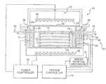
- FIG. 1is a cross-sectional, diagrammatical view of one embodiment of a multiwafer thermal processing system made in accordance with the present invention
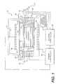
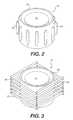
- FIG. 2is a perspective view of one embodiment of a lamp configuration that can be used in the thermal processing system of the present invention
- FIG. 3is a perspective view of an alternative embodiment of a lamp configuration for use in thermal processing systems of the present invention
- FIG. 4is a perspective view of an alternative embodiment of a thermal processing system made in accordance with the present invention.
- FIG. 5is a cross-sectional view of a further alternative embodiment of a thermal processing system made in accordance with the present invention.
- FIG. 6is a cross-sectional view of a lamp and an energy dispersing member which may be used in the thermal processing system illustrated in FIG. 5;
- FIG. 7is a top view of the lamp and energy dispersing member illustrated in FIG. 6 .
- the present inventionis directed to a thermal processing system capable of heat treating a plurality of semiconductor wafers at the same time.
- the systemcan be designed to heat the semiconductor wafers very quickly, at a controlled rate, and can also heat the wafers substantially uniformly.
- the systemincludes a thermal processing chamber in communication with a heating device that is used to heat treat the semiconductor wafers contained in the chamber.
- the heating devicecontains a plurality of light energy sources, such as lamps, that are positioned so as to surround the thermal processing chamber for heating the wafers.
- the lampscan be used to directly heat the semiconductor wafers or can be used to indirectly heat the semiconductor wafers.
- the semiconductor wafersare held on a substrate holder.
- the substrate holderis designed to hold the wafers in a stacked arrangement.
- the wafersshould be positioned so that a space is present in between adjacent wafers.
- the system of the present inventioncan further include a method of monitoring the temperature of the wafers during heat treating.
- temperature sensing devicessuch as pyrometers and/or thermocouples can be placed within the system at various locations.
- the temperature sensing devicescan be used to monitor the temperature of the wafers directly or can be used to monitor the temperature of an object in the chamber which can be used to determine the temperature of the wafers.
- the energy being emitted by the lampscan be selectively controlled for maintaining the wafers at a substantially constant temperature and for heating the wafers according to a preset pattern.
- System 10includes a processing chamber 12 adapted to receive a plurality of wafers 14 for conducting various processes.
- Wafers 14can be made from various materials such as silicon. Wafers 14 can be placed in chamber 12 in order to anneal the wafers or to form coatings on the wafers by reacting the wafers with a gas being circulated through the chamber. As shown, wafers 14 are positioned on a substrate holder 15 made from a thermal insulating material such as quartz. Chamber 12 is designed to heat wafers 14 at very rapid rates and under carefully controlled conditions. Chamber 12 can be made from various materials, including metals and ceramics. For instance, chamber 12 can be made from stainless steel or quartz.
- chamber 12When chamber 12 is made from a heat conductive material, preferably the chamber includes a cooling system.
- chamber 12includes a cooling conduit 16 wrapped around the perimeter of the chamber.
- Conduit 16is adapted to circulate a cooling fluid, such as water, which is used to maintain the walls of chamber 12 at a constant temperature.
- Chamber 12can also include a gas inlet 18 and a gas outlet 20 for introducing a gas into the chamber and/or for maintaining the chamber within a preset pressure range.
- gas inlet 18includes a spray nozzle 19 defining a plurality of openings. Spray nozzle 19 is for evenly distributing the gas across the surface of the wafers.
- a gascan be introduced into chamber 12 through gas inlet 18 for reaction with wafers 14 . Once processed, the gas can then be evacuated from the chamber using gas outlet 20 .
- an inert gascan be fed to chamber 12 through gas inlet 18 for preventing any unwanted or undesirable side reactions from occurring within the chamber.
- gas inlet 18 and gas outlet 20can be used to pressurize chamber 12 .
- a vacuumcan also be created in chamber 12 when desired, using gas outlet 20 or an additional larger outlet positioned beneath the level of the wafer.
- substrate holder 15is designed to hold the wafers in a stacked arrangement.
- substrate holder 15is designed to maintain a determined distance between adjacent wafers.
- the wafersare spaced a distance sufficient to allow light energy and gases entering the chamber to distribute uniformly over the wafers. Specifically, it is important that each of the wafers be contacted with light energy across their entire surface so that the wafers can be heated quickly and uniformly. For most applications, the wafers should be spaced between about 1 ⁇ 4 inch to about 1.0 inch apart. The actual distance between the wafers, however, will depend upon the size of the wafers and the amount of light energy entering the chamber.
- substrate holder 15can be adapted to rotate wafers 14 using a wafer rotation mechanism 21 . Rotating the wafers promotes greater temperature uniformity over the surface of the wafers and promotes enhanced contact between wafers 14 and any gases introduced into the chamber.
- a heat source or heating device generally 22is included in communication with chamber 12 for heating wafers 14 during processing.
- heating device 22is preferably made up of a plurality of lamps 24 , such as tungsten-halogen lamps. As shown in the embodiment illustrated in FIG. 1, lamps 24 completely encircle thermal processing chamber 12 . Lamps 24 are also positioned at the top of the chamber and at the bottom of the chamber. In general, it is preferred that the system of the present invention include many lamps in order to heat the plurality of wafers 14 rapidly and in order to provide controls for heating the wafers uniformly.
- lamps 24as a heat source is generally preferred. For instance, lamps have much higher heating and cooling rates than other heating devices, such as electrical elements or conventional furnaces. Lamps 24 create a rapid processing system that provide instantaneous energy, typically requiring a very short and well controlled start up period. The flow of energy from lamps 24 can also be abruptly stopped at any time. As shown in the figure, lamps 24 can be connected to a gradual power controller 25 that can be used to increase or decrease the light energy being emitted by any of the lamps or any group of lamps.
- the lampsare associated with reflectors 36 .
- a set of reflectors 36can be positioned behind the lamps which reflect light energy being emitted by the lamps towards the semiconductor wafers.
- Reflectors 36can be in the shape of reflective annular recesses that surround a portion of lamps 24 or that are in the shape of light pipes that completely surround the lamps and extend beyond the length of the lamps.
- the lamps that are used in the system of the present inventioncan have various shapes and can be positioned in various different configurations surrounding the thermal processing chamber.
- the lamps surrounding the sides of the chamberhave an elongated tubular housing that are positioned such that the elongated housing faces the thermal processing chamber.
- FIGS. 2 and 3two different configurations illustrating lamps of this type are shown in FIGS. 2 and 3.
- thermal processing chamber 12is shown surrounded by a plurality of lamps 24 .
- lamps 24are vertically oriented with respect to the chamber or, in other words, are positioned parallel to the central axis of the chamber.
- lamps 24are horizontally positioned with respect to thermal processing chamber 12 . More particularly, lamps 24 as shown in FIG. 3 are assembled in an interlocking stacked arrangement that forms the shape of a square. Thermal processing chamber 12 containing wafers 14 is positioned within the square.
- lamps 24can also be positioned in various other arrangements and configurations.
- annular lampscan be formed that encircle thermal processing chamber 12 .
- shorter upright lampsmay also be used, especially for being placed on the top and at the bottom of the thermal processing chamber.
- An upright lamprefers to a shorter lamp having a free open end opposite an end that is adapted to be placed into a socket. When incorporated into the system of the present invention, such lamps can be positioned such that the open free end faces the thermal processing chamber. Upright lamps are better adapted to focusing high intensity light onto a particular area.
- the elongated lamps shown in FIGS. 2 and 3, however,are well suited to exposing large areas to high intensity light.
- thermal processing chamber 12includes plurality of radiation sensing devices generally 27 .
- Radiation sensing devices 27include a plurality of optical fibers or light pipes 28 which are, in turn, in communication with a plurality of corresponding light detectors 30 .
- Optical fibers 28are configured to receive thermal energy being emitted by corresponding wafers 14 at a particular wavelength. The amount of sensed radiation is then communicated to light detectors 30 which generate a usable voltage signal for determining the temperature of the wafer which can be calculated based, in part, on Planck's Law.
- optical fibers 28can be positioned so that they receive a direct measurement of the amount of thermal energy being emitted by wafers 14 . Since the wafers are stacked in the system of the present invention, however, it may be difficult to position optical fibers 28 to receive a direct measurement of the wafers. If this is the case, however, the wafer temperature can be calculated from a glancing angle measurement.
- each optical fiber 28 in combination with a light detector 30comprises a pyrometer.
- the optical fibers 28are routed to a single but multiplexing radiation sensing device.
- thermal processing chamber 12can contain one or a plurality of radiation sensing devices.
- thermal processing chamber 12contains a plurality of radiation sensing devices that measure the temperature of each of the wafers. Knowing the temperature of each of the wafers can then be used to control the amount of heat being applied to the wafers as will be described in more detail hereinafter.
- system 10should be designed such that lamps 24 are separated from the interior of the thermal processing chamber.
- system 10includes a top window 32 , a bottom window 35 , and a cylindrical window 33 , as particularly shown in FIGS. 2 and 3.
- Windows 32 , 35 and 33are made from a transparent material that allows light energy being emitted by lamps 24 to heat wafers 14 , while creating a sealed chamber in order to prevent the wafers from being contaminated by the lamps or from any other source.
- windows 32 , 33 and 35can also act as a filter in preventing thermal radiation being emitted by lamps 24 at the wavelength at which light detectors 30 operate from entering thermal processing chamber 12 .
- windows 32 , 33 and 35can be made from fused silica or quartz. Fused silica is known to absorb thermal radiation very effectively at selected wavelengths. For instance, synthetic fused silica with high concentration of OH ions is very effective at absorbing light at a wavelength of from approximately 2.7 micrometers to about 2.8 micrometers.
- light detectors 30can be configured to detect thermal radiation being emitted by wafers 14 at a wavelength of about 2.7 micrometers.
- the separation between radiation arriving to the sensors from the wafer and lampsis achieved by mechanical means of isolation.
- buffers and shieldsare present to prevent a direct path from forming between a light source and a sensing port.
- thermocouplesmay be incorporated into the system for monitoring the temperature of the wafers at a single location or at a plurality of locations.
- the thermocouplescan be placed in direct contact with the wafers or can be placed adjacent the wafers from which the temperature can be extrapolated.
- thermocouplescan be incorporated into substrate holder 15 for monitoring the temperature of the wafers.
- System 10further includes a system controller 50 which can be, for instance, a microprocessor. Controller 50 receives voltage signals from light detectors 30 that represent the radiation amounts being sampled at the various locations. Controller 50 can also be connected to any thermocouples contained within the system for receiving temperature information. Based on the signals received, controller 50 is configured to calculate the temperature of wafers 14 at one or more locations.
- a system controller 50which can be, for instance, a microprocessor. Controller 50 receives voltage signals from light detectors 30 that represent the radiation amounts being sampled at the various locations. Controller 50 can also be connected to any thermocouples contained within the system for receiving temperature information. Based on the signals received, controller 50 is configured to calculate the temperature of wafers 14 at one or more locations.
- System controller 50 as shown in FIG. 1can also be in communication with lamp power controller 25 .
- controller 50can determine the temperature of wafers 14 , and, based on this information, control the amount of thermal energy being emitted by lamps 24 .
- controller 50can control all of the lamps together, can individually control the lamps, or can control the lamps in selected groups. In this manner, instantaneous adjustments can be made regarding the conditions within reactor 12 for processing wafers 14 within carefully controlled limits.
- controller 50can also be used to automatically control other elements within the system. For instance, controller 50 can be used to control the flow rate of gases entering chamber 12 through gas inlet 18 . As shown, controller 50 can further be used to control the rate at which wafers 14 are rotated within the chamber.
- chamber 12includes a lining 62 made from an opaque heat conductive material.
- Lining 62includes a top 64 , a bottom 68 , and a cylindrical sleeve 66 which serve to completely surround wafers 14 held on substrate holder 15 .
- lamps 24are used to heat lining 62 which in turn heats wafers 14 .
- the wafersare heated indirectly.
- Lining 62 of thermal processing chamber 12can be made from various materials.
- lining 62is made from silicon carbide.
- itis made from a polysilicon material.
- the system illustrated in FIG. 4can include temperature devices which directly measure the temperature of the wafers 14 during processing, similar to the temperature devices illustrated in FIG. 1 .
- the temperature of wafers 14can be determined and calculated by measuring the temperature of lining 62 during processing.
- lining 62can be calibrated such that by knowing the temperature of the lining, the temperature of the wafers inside the lining can be estimated.
- temperature sensing devicesare required that sense the temperature of lining 62 .
- a radiation sensing device 30can be used to monitor the temperature of lining 62 and/or a thermocouple 60 can also be built into the lining for providing temperature information. Radiation sensing device 30 and thermocouple 60 can be connected to a controller which can be designed to then determine the temperature of wafers 14 based on the temperature information that is received.
- FIG. 5a further alternative embodiment of a heating system made in accordance with the present invention is illustrated.
- energy dispersing members 70are placed within the thermal processing chamber adjacent to wafers 14 .
- energy dispersing members 70are placed in between adjacent wafers.
- Energy dispersing members 70are designed to receive light energy from lamps 24 and to refract and disperse the light energy onto the wafers in order to heat the wafers uniformly.
- one of the objectives of the present inventionis to ensure that light energy reaches and contacts each of the wafers contained on substrate holder 15 .
- the wafersare spaced a determined distance apart.
- energy dispersing members 70are specifically included to ensure that the entire top surface and bottom surface of the wafers are being contacted by light energy and being heated during the process.
- one or more lamps 24are positioned around the perimeter or periphery of energy dispersing members 70 for shining light energy into the sides of the energy dispersing members.
- Reflectors 36can also be provided for directing and focusing the light energy being emitted by lamps 24 directly into energy dispersing members 70 .
- FIGS. 6 and 7light energy entering energy dispersing members 70 is then refracted and dispersed in multiple directions.
- Energy dispersing members 70can be made from various materials and can have various shapes.
- energy dispersing members 70comprise quartz plates containing areas having a different index of refraction 72 than the quartz material itself as shown in FIG. 6 .
- Areas 72 having a different index of refractioncan be, for instance, glass particles, such as glass spheres, or air bubbles.
- energy dispersing members 70can be made from a substantially transparent material, such as quartz, that is shaped to refract and reflect the light energy as desired. For instance, sharp angles can be formed into the quartz plate that cause light energy entering the plate be directed towards the semiconductor wafers 14 .
- energy dispersing members 70can embody glass spheres in paste using screen printing and high temperature fusing.
- a transparent substrate made from a material such as quartzcan be screen printed with a paste that contains glass particles, such as spheres, and a glass frit material.
- the pastecan be screen printed on the substrate.
- the substratecan then be heated in order to drive off any organic binders and in order to form a heat resistant coating on the substrate capable of uniformly dispersing light energy contacting the substrate.
- the pastecan be screen printed onto the substrate according to any particular design or pattern in order to control the light scattering properties of the final product.
- energy dispersing members 70can be made to disperse light according to a desired and predetermined pattern. For instance, in order to ensure that wafers 14 are being heated uniformly, energy dispersing members 70 can be designed so that more light energy is contacting the wafers at the perimeter where typically more heat is needed in order to compensate for energy losses at the edges of the wafer. It should be understood, however, that any desired or predetermined spectral pattern can be created in accordance with the present invention.
- the systemincludes a radiation sensing device 30 for determining the temperature of wafers 14 during processing.
- a radiation sensing device 30for determining the temperature of wafers 14 during processing.
- the same type of temperature measurement devices illustrated in FIG. 1may be used.
- Lamps 24 that can be used in the embodiment illustrated in FIG. 5can vary depending upon the particular application.
- elongated lamps as shown in FIG. 7may be used or, alternatively, instead of one elongated lamp, the system can include a row of short upright lamps.
- lampsare positioned to completely surround energy dispersing members 70 .
- lamps 24 surrounding energy dispersing members 70should emit enough light energy so that each surface of the wafer is contacted with at least 6 watts/cm 2 of power.
- the system of the present invention as shown in FIG. 5can be used for various processes and is particularly well suited for low temperature applications.
- the systemis well suited for copper annealing, copper reflow, low K dielectric annealing, aluminum sintering, besides various other processes.
- the systemcan also be used for deposition processes using proper gases in combination with the heating sources to deposit low and high K materials, dielectric materials and the like.
Landscapes
- Engineering & Computer Science (AREA)
- Physics & Mathematics (AREA)
- Condensed Matter Physics & Semiconductors (AREA)
- General Physics & Mathematics (AREA)
- Manufacturing & Machinery (AREA)
- Computer Hardware Design (AREA)
- Microelectronics & Electronic Packaging (AREA)
- Power Engineering (AREA)
- Health & Medical Sciences (AREA)
- Toxicology (AREA)
- Electrodes Of Semiconductors (AREA)
Abstract
Description
The present application is a Continuation Application of U.S. Ser. No.: 09/759,426 filed on Jan. 12, 2001 and is also a continuation of U.S. Ser. No. 09/208,958 filed on Dec. 10,1998 is now U.S. Pat. No. 6,310,328.
The present invention is generally directed to rapid thermal processing chambers for heating semiconductor wafers using light energy. More particularly, the present invention is directed to rapid thermal processing chambers that are capable of processing a plurality of wafers at the same time.
Various heating devices have been proposed in the past for processing semiconductor wafers. These heating devices can be classified into two basic configurations. The first is a batch system in which multiple wafers (25 wafers to about 200 wafers) are loaded into a round tubular furnace and slowly heated to the desired temperature. Batch systems can be considered temperature equilibrium devices in that the furnace walls are approximately at the same temperature as the heating elements and the wafers being heated. Batch systems are typically referred to as “hot wall” systems since the furnace walls are at an elevated temperature. The primary advantage of a batch system is the ability to process many wafers at the same time therefore reducing the processing cost per wafer. The disadvantage of such a configuration, however, is the speed in which the wafer temperature can be elevated or cooled. The large thermal mass of a batch furnace prevents quick temperature changes and forces relatively long process times, ranging from about fifteen minutes to about five hours.
A second and newer approach to wafer heating is rapid thermal processing where a single wafer is heated in a small compartment using radiant energy as the energy source. For instance, such systems typically include a substrate holder for holding a semiconductor wafer and a light source that emits light energy for heating the wafer. During heat treatment, the semiconductor wafer is heated under controlled conditions according to a preset temperature regime. For monitoring the temperature of the semiconductor wafer during heat treatment, rapid thermal processing chambers also typically include temperature sensing devices, such as pyrometers, that sense the radiation being emitted by a semiconductor wafer at a selected band or wavelength. By sensing the thermal radiation being emitted by the wafer, the temperature of the wafer can be calculated with reasonable accuracy.
In alternative embodiments, instead of or in addition to using radiation sensing devices, rapid thermal processing chambers can also contain thermocouples for monitoring the temperature of the wafers. Thermocouples measure the temperature of objects by direct contact.
Many semiconductor heating processes require a wafer to be heated to high temperatures so that various chemical and physical reactions can take place as the wafer is fabricated into a device. During rapid thermal processing, semiconductor wafers are typically heated by arrays of lights to temperatures, for instance, from about 400° C. to about 1,200° C., for times which are typically less than a few minutes and in most cases less than one minute.
Rapid thermal processing chambers typically operate in a non-equilibrium state. Specifically, the walls surrounding the wafer are kept cool, with active cooling, and thus are typically referred to as “cold wall” systems. The non-equilibrium configuration refers to the fact that the filament temperature inside the radiant source is at a much higher temperature than the wafer. The key advantage of using rapid thermal processing systems is the ability to quickly change wafer temperature therefore enabling very short heating cycles which can be between about one second to about two minutes. The drawback of rapid thermal processing systems, however, is the cost per wafer processed, especially for cycles between 60 and 120 seconds long, since the systems are only equipped to heat one wafer at a time.
In view of the above, a need currently exists for a thermal processing chamber that is capable of rapidly heat treating a plurality of wafers at the same time. Specifically, a need exists for a thermal processing chamber capable of accommodating a plurality of wafers as in a batch system, but yet also capable of processing the wafers very rapidly, such as in a rapid thermal processing system.
The present invention recognizes and addresses the foregoing disadvantages and others of prior art constructions and methods.
Accordingly, it is an object of the present invention to provide an improved thermal processing chamber for heat treating semiconductor wafers.
Another object of the present invention is to provide a thermal processing chamber that is capable of heat treating a plurality of wafers at the same time.
Still another object of the present invention is to provide a multiwafer thermal processing chamber that heats the wafers using light energy.
Another object of the present invention is to provide a multiwafer thermal processing system that rapidly processes a plurality of semiconductor wafers in a “cold wall” chamber.
These and other objects of the present invention are achieved by providing a multiwafer thermal processing system. The system includes a thermal processing chamber adapted to receive a plurality of stacked semiconductor wafers. A plurality of light energy sources are placed in communication with the thermal processing chamber for the heating semiconductor wafers contained in the chamber. Specifically, the plurality of light energy sources are positioned so as to encircle the thermal processing chamber. Light energy sources can also be placed at the top and at the bottom of the chamber if desired.
A substrate holder is contained within the thermal processing chamber. The substrate holder is configured to hold the plurality of semiconductor wafers. In particular, the wafers are held in a stacked arrangement wherein adjacent wafers are spaced a distance sufficient for light energy being emitted by the light energy sources to contact the entire bottom and top surfaces of the wafers.
In one embodiment, the system further includes at least one temperature sensing device for monitoring the temperature of the semiconductor wafers. For instance, the temperature sensing devices can be pyrometers, thermocouples or a combination of pyrometers and thermocouples. A controller, such as a microprocessor is placed in communication with the temperature sensing devices and the light energy sources. The controller is configured to control the amount of light energy being emitted by the light energy sources in response to temperature information received from the temperature sensing devices. In this manner, the wafers can be heated uniformly and according to a preset temperature regime.
The system of the present invention is capable of heating a plurality of semiconductor wafers (from 2 to 10 wafers) to a temperature range from 200° C. to 1,200° C. The system is capable of heating wafers to the above described temperatures in a very short period of time, such as from about one minute to about five minutes.
For most applications, the light energy sources should be positioned outside of the thermal processing chamber so the light energy sources do not contaminate wafers contained in the chamber. In one embodiment, the thermal processing chamber can include one or more windows designed to allow light energy being emitted by the light energy sources to pass into the chamber.
The light energy sources used in the system of the present invention can have various shapes and can be positioned around the thermal processing chamber at various locations and according to various patterns. In one embodiment, the light energy sources can comprise lamps having an elongated housing. The lamps can be positioned such that the elongated housing faces the thermal processing chamber. The lamps can be placed around the thermal processing chamber so that the elongated housing is parallel to a vertical axis of the chamber. Alternatively, the lamps can be placed perpendicular to the vertical axis of the chamber. Preferably, the system includes reflectors positioned behind the light energy sources. The reflectors can be used to direct light energy being emitted by the light energy sources into the thermal processing chamber.
In an alternative embodiment of the present invention, instead of the light energy sources directly heating the semiconductor wafers, the light energy sources can be used to heat a thermally conductive lining which in turn heats the wafers. For instance, the thermal processing system of the present invention can contain a lining that is positioned so as to surround semiconductor wafers held on the substrate holder in the thermal processing chamber. The lining can be in the shape of a cylindrical sleeve that can have a top and a bottom for completely enclosing the substrate holder and the wafers. The thermally conductive lining can be made from various materials including, for instance, silicon carbide.
In this embodiment, in order to monitor the temperature of the wafers during processing, one or more temperature sensing devices can be used to sense the temperature of the thermally conductive lining. The system can be calibrated such that the temperature of the wafers contained within the thermal processing chamber can be determined by knowing the temperature of the lining.
In a further alternative embodiment of the present invention, the multiwafer thermal processing system can include energy dispersing members located within the thermal processing chamber for distributing light energy being emitted by the light energy sources onto the semiconductor wafers. For instance, in one embodiment, the energy dispersing members can be in the shape of plates spaced in between semiconductor wafers held within the chamber. Light energy sources can be positioned to emit light energy directly into the energy dispersing members. The energy dispersing members can redirect the light energy onto the adjacent wafers.
The energy dispersing members can be made from various materials and can have any shape sufficient to refract and disperse light. In one embodiment, the energy dispersing members can be quartz plates containing areas having a different index of refraction than the quartz. For instance, the areas having a different index of refraction can be made from glass particles, such as glass spheres.
In an alternative embodiment, the energy dispersing members can be quartz plates having a shape that is designed to refract light. For instance, sharp angles can be formed into the quartz plate which cause light energy in the plate to be scattered in various directions. Preferably, light energy sources are positioned adjacent the side surfaces of each of the energy dispersing members. In this manner, light energy directly enters the dispersing members and is distributed to adjacent wafers. In order to maximize the amount of light energy that enters the light dispersing members, reflectors can also be placed around the light energy sources.
Other objects, features and aspects of the present invention are discussed in greater detail below.
A full and enabling disclosure of the present invention, including the best mode thereof, directed to one of ordinary skill in the art, is set forth more particularly in the remainder of the specification, which makes reference to the appended figures in which:
FIG. 1 is a cross-sectional, diagrammatical view of one embodiment of a multiwafer thermal processing system made in accordance with the present invention;
FIG. 2 is a perspective view of one embodiment of a lamp configuration that can be used in the thermal processing system of the present invention;
FIG. 3 is a perspective view of an alternative embodiment of a lamp configuration for use in thermal processing systems of the present invention;
FIG. 4 is a perspective view of an alternative embodiment of a thermal processing system made in accordance with the present invention;
FIG. 5 is a cross-sectional view of a further alternative embodiment of a thermal processing system made in accordance with the present invention;
FIG. 6 is a cross-sectional view of a lamp and an energy dispersing member which may be used in the thermal processing system illustrated in FIG. 5; and
FIG. 7 is a top view of the lamp and energy dispersing member illustrated in FIG.6.
Repeat use of references characters in the present specification and drawings is intended to represent same or analogous features or elements of the invention.
It is to be understood by one of ordinary skill in the art that the present discussion is a description of exemplary embodiments only, and is not intended as limiting the broader aspects of the present invention, which broader aspects are embodied in the exemplary construction.
In general, the present invention is directed to a thermal processing system capable of heat treating a plurality of semiconductor wafers at the same time. The system can be designed to heat the semiconductor wafers very quickly, at a controlled rate, and can also heat the wafers substantially uniformly. The system includes a thermal processing chamber in communication with a heating device that is used to heat treat the semiconductor wafers contained in the chamber. The heating device contains a plurality of light energy sources, such as lamps, that are positioned so as to surround the thermal processing chamber for heating the wafers. According to the present invention, the lamps can be used to directly heat the semiconductor wafers or can be used to indirectly heat the semiconductor wafers.
During heating, the semiconductor wafers are held on a substrate holder. The substrate holder is designed to hold the wafers in a stacked arrangement. For most applications, the wafers should be positioned so that a space is present in between adjacent wafers.
The system of the present invention can further include a method of monitoring the temperature of the wafers during heat treating. For instance, temperature sensing devices such as pyrometers and/or thermocouples can be placed within the system at various locations. The temperature sensing devices can be used to monitor the temperature of the wafers directly or can be used to monitor the temperature of an object in the chamber which can be used to determine the temperature of the wafers. In one embodiment, based upon the temperature being sensed during processing, the energy being emitted by the lamps can be selectively controlled for maintaining the wafers at a substantially constant temperature and for heating the wafers according to a preset pattern.
Referring to FIG. 1, a system generally10 made in accordance with the present invention for heat treating a plurality of semiconductor wafers simultaneously is illustrated.System 10 includes aprocessing chamber 12 adapted to receive a plurality ofwafers 14 for conducting various processes.Wafers 14 can be made from various materials such as silicon.Wafers 14 can be placed inchamber 12 in order to anneal the wafers or to form coatings on the wafers by reacting the wafers with a gas being circulated through the chamber. As shown,wafers 14 are positioned on asubstrate holder 15 made from a thermal insulating material such as quartz.Chamber 12 is designed to heatwafers 14 at very rapid rates and under carefully controlled conditions.Chamber 12 can be made from various materials, including metals and ceramics. For instance,chamber 12 can be made from stainless steel or quartz.
Whenchamber 12 is made from a heat conductive material, preferably the chamber includes a cooling system. For instance, as shown in FIG. 1,chamber 12 includes acooling conduit 16 wrapped around the perimeter of the chamber.Conduit 16 is adapted to circulate a cooling fluid, such as water, which is used to maintain the walls ofchamber 12 at a constant temperature.
Alternatively, an inert gas can be fed tochamber 12 throughgas inlet 18 for preventing any unwanted or undesirable side reactions from occurring within the chamber. In a further embodiment,gas inlet 18 andgas outlet 20 can be used to pressurizechamber 12. A vacuum can also be created inchamber 12 when desired, usinggas outlet 20 or an additional larger outlet positioned beneath the level of the wafer.
As shown,substrate holder 15 is designed to hold the wafers in a stacked arrangement. In the embodiment illustrated in FIG. 1,substrate holder 15 is designed to maintain a determined distance between adjacent wafers. The wafers are spaced a distance sufficient to allow light energy and gases entering the chamber to distribute uniformly over the wafers. Specifically, it is important that each of the wafers be contacted with light energy across their entire surface so that the wafers can be heated quickly and uniformly. For most applications, the wafers should be spaced between about ¼ inch to about 1.0 inch apart. The actual distance between the wafers, however, will depend upon the size of the wafers and the amount of light energy entering the chamber.
During processing,substrate holder 15, in one embodiment, can be adapted to rotatewafers 14 using awafer rotation mechanism 21. Rotating the wafers promotes greater temperature uniformity over the surface of the wafers and promotes enhanced contact betweenwafers 14 and any gases introduced into the chamber.
A heat source or heating device generally22 is included in communication withchamber 12 forheating wafers 14 during processing. As described above,heating device 22 is preferably made up of a plurality oflamps 24, such as tungsten-halogen lamps. As shown in the embodiment illustrated in FIG. 1,lamps 24 completely encirclethermal processing chamber 12.Lamps 24 are also positioned at the top of the chamber and at the bottom of the chamber. In general, it is preferred that the system of the present invention include many lamps in order to heat the plurality ofwafers 14 rapidly and in order to provide controls for heating the wafers uniformly.
The use oflamps 24 as a heat source is generally preferred. For instance, lamps have much higher heating and cooling rates than other heating devices, such as electrical elements or conventional furnaces.Lamps 24 create a rapid processing system that provide instantaneous energy, typically requiring a very short and well controlled start up period. The flow of energy fromlamps 24 can also be abruptly stopped at any time. As shown in the figure,lamps 24 can be connected to agradual power controller 25 that can be used to increase or decrease the light energy being emitted by any of the lamps or any group of lamps.
In order to assist in directing the light energy being emitted bylamps 24 intochamber 12 and ontowafers 14, preferably the lamps are associated withreflectors 36. For instance, as shown in FIG. 1, a set ofreflectors 36 can be positioned behind the lamps which reflect light energy being emitted by the lamps towards the semiconductor wafers.Reflectors 36 can be in the shape of reflective annular recesses that surround a portion oflamps 24 or that are in the shape of light pipes that completely surround the lamps and extend beyond the length of the lamps.
The lamps that are used in the system of the present invention can have various shapes and can be positioned in various different configurations surrounding the thermal processing chamber. For example, in one embodiment, the lamps surrounding the sides of the chamber have an elongated tubular housing that are positioned such that the elongated housing faces the thermal processing chamber. For instance, two different configurations illustrating lamps of this type are shown in FIGS. 2 and 3.
Referring to FIG. 2,thermal processing chamber 12 is shown surrounded by a plurality oflamps 24. In this embodiment,lamps 24 are vertically oriented with respect to the chamber or, in other words, are positioned parallel to the central axis of the chamber.
In the embodiment shown in FIG. 3, on the other hand,lamps 24 are horizontally positioned with respect tothermal processing chamber 12. More particularly,lamps 24 as shown in FIG. 3 are assembled in an interlocking stacked arrangement that forms the shape of a square.Thermal processing chamber 12 containingwafers 14 is positioned within the square.
It should be understood, however, that besides the arrangements illustrated in FIGS. 2 and 3,lamps 24 can also be positioned in various other arrangements and configurations. For instance, in one embodiment, annular lamps can be formed that encirclethermal processing chamber 12.
Besides lamps having an elongated housing, shorter upright lamps may also be used, especially for being placed on the top and at the bottom of the thermal processing chamber. An upright lamp refers to a shorter lamp having a free open end opposite an end that is adapted to be placed into a socket. When incorporated into the system of the present invention, such lamps can be positioned such that the open free end faces the thermal processing chamber. Upright lamps are better adapted to focusing high intensity light onto a particular area. The elongated lamps shown in FIGS. 2 and 3, however, are well suited to exposing large areas to high intensity light.
In order to monitor the temperature ofwafers 14 during the heating process, in the embodiment shown in FIG. 1,thermal processing chamber 12 includes plurality of radiation sensing devices generally27.Radiation sensing devices 27 include a plurality of optical fibers orlight pipes 28 which are, in turn, in communication with a plurality of correspondinglight detectors 30.Optical fibers 28 are configured to receive thermal energy being emitted by correspondingwafers 14 at a particular wavelength. The amount of sensed radiation is then communicated tolight detectors 30 which generate a usable voltage signal for determining the temperature of the wafer which can be calculated based, in part, on Planck's Law.
Preferably,optical fibers 28 can be positioned so that they receive a direct measurement of the amount of thermal energy being emitted bywafers 14. Since the wafers are stacked in the system of the present invention, however, it may be difficult to positionoptical fibers 28 to receive a direct measurement of the wafers. If this is the case, however, the wafer temperature can be calculated from a glancing angle measurement.
In one embodiment, eachoptical fiber 28 in combination with alight detector 30 comprises a pyrometer. In another embodiment, theoptical fibers 28, are routed to a single but multiplexing radiation sensing device.
In general,thermal processing chamber 12 can contain one or a plurality of radiation sensing devices. In a preferred embodiment, as shown in FIG. 1,thermal processing chamber 12 contains a plurality of radiation sensing devices that measure the temperature of each of the wafers. Knowing the temperature of each of the wafers can then be used to control the amount of heat being applied to the wafers as will be described in more detail hereinafter.
In one preferred embodiment of the present invention,system 10 should be designed such thatlamps 24 are separated from the interior of the thermal processing chamber. In this regard,system 10 includes atop window 32, abottom window 35, and acylindrical window 33, as particularly shown in FIGS. 2 and 3.Windows lamps 24 to heatwafers 14, while creating a sealed chamber in order to prevent the wafers from being contaminated by the lamps or from any other source.
In one embodiment,windows lamps 24 at the wavelength at whichlight detectors 30 operate from enteringthermal processing chamber 12. For example, in one embodiment,windows windows light detectors 30 can be configured to detect thermal radiation being emitted bywafers 14 at a wavelength of about 2.7 micrometers.
In other embodiments, however, the separation between radiation arriving to the sensors from the wafer and lamps is achieved by mechanical means of isolation. In these embodiments, buffers and shields are present to prevent a direct path from forming between a light source and a sensing port.
Besides using radiation sensing devices, other temperature sensing devices may be used in the system of the present invention. For instance, one or more thermocouples may be incorporated into the system for monitoring the temperature of the wafers at a single location or at a plurality of locations. The thermocouples can be placed in direct contact with the wafers or can be placed adjacent the wafers from which the temperature can be extrapolated. For example, in one embodiment, thermocouples can be incorporated intosubstrate holder 15 for monitoring the temperature of the wafers.
In one embodiment,controller 50 can also be used to automatically control other elements within the system. For instance,controller 50 can be used to control the flow rate ofgases entering chamber 12 throughgas inlet 18. As shown,controller 50 can further be used to control the rate at whichwafers 14 are rotated within the chamber.
Referring to FIG. 4, an alternative embodiment of athermal processing chamber 12 for use in the heating system of the present invention is illustrated. In this embodiment,chamber 12 includes a lining62 made from an opaque heat conductive material.Lining 62 includes a top64, a bottom68, and acylindrical sleeve 66 which serve to completely surroundwafers 14 held onsubstrate holder 15. In this embodiment,lamps 24 are used to heat lining62 which in turn heatswafers 14. Thus, the wafers are heated indirectly.
Lining62 ofthermal processing chamber 12 can be made from various materials. In one preferred embodiment for instance, lining62 is made from silicon carbide. In another preferred embodiment it is made from a polysilicon material.
In order to monitor the temperatures ofwafers 14 during heating the system illustrated in FIG. 4 can include temperature devices which directly measure the temperature of thewafers 14 during processing, similar to the temperature devices illustrated in FIG.1.
Alternatively, the temperature ofwafers 14 can be determined and calculated by measuring the temperature of lining62 during processing. Specifically, lining62 can be calibrated such that by knowing the temperature of the lining, the temperature of the wafers inside the lining can be estimated. In this embodiment, temperature sensing devices are required that sense the temperature of lining62. For example, as shown in FIG. 4, aradiation sensing device 30 can be used to monitor the temperature of lining62 and/or athermocouple 60 can also be built into the lining for providing temperature information.Radiation sensing device 30 andthermocouple 60 can be connected to a controller which can be designed to then determine the temperature ofwafers 14 based on the temperature information that is received.
Referring to FIG. 5, FIG.6 and FIG. 7, a further alternative embodiment of a heating system made in accordance with the present invention is illustrated. In this embodiment,energy dispersing members 70 are placed within the thermal processing chamber adjacent towafers 14. In particular,energy dispersing members 70 are placed in between adjacent wafers.Energy dispersing members 70 are designed to receive light energy fromlamps 24 and to refract and disperse the light energy onto the wafers in order to heat the wafers uniformly.
As described above, one of the objectives of the present invention is to ensure that light energy reaches and contacts each of the wafers contained onsubstrate holder 15. Thus, in FIG. 1, the wafers are spaced a determined distance apart. In this embodiment, on the other hand,energy dispersing members 70 are specifically included to ensure that the entire top surface and bottom surface of the wafers are being contacted by light energy and being heated during the process.
As shown in FIG. 5, preferably one ormore lamps 24 are positioned around the perimeter or periphery ofenergy dispersing members 70 for shining light energy into the sides of the energy dispersing members.Reflectors 36 can also be provided for directing and focusing the light energy being emitted bylamps 24 directly intoenergy dispersing members 70. As particularly shown in FIGS. 6 and 7, light energy enteringenergy dispersing members 70 is then refracted and dispersed in multiple directions.
Alternatively,energy dispersing members 70 can be made from a substantially transparent material, such as quartz, that is shaped to refract and reflect the light energy as desired. For instance, sharp angles can be formed into the quartz plate that cause light energy entering the plate be directed towards thesemiconductor wafers 14.
In still another alternative embodiment,energy dispersing members 70 can embody glass spheres in paste using screen printing and high temperature fusing. For instance, a transparent substrate made from a material such as quartz can be screen printed with a paste that contains glass particles, such as spheres, and a glass frit material. The paste can be screen printed on the substrate. Once the paste is applied to the substrate, the substrate can then be heated in order to drive off any organic binders and in order to form a heat resistant coating on the substrate capable of uniformly dispersing light energy contacting the substrate. In this embodiment, the paste can be screen printed onto the substrate according to any particular design or pattern in order to control the light scattering properties of the final product.
In any of the above embodiments,energy dispersing members 70 can be made to disperse light according to a desired and predetermined pattern. For instance, in order to ensure thatwafers 14 are being heated uniformly,energy dispersing members 70 can be designed so that more light energy is contacting the wafers at the perimeter where typically more heat is needed in order to compensate for energy losses at the edges of the wafer. It should be understood, however, that any desired or predetermined spectral pattern can be created in accordance with the present invention.
As shown in FIG. 5, in this embodiment, the system includes aradiation sensing device 30 for determining the temperature ofwafers 14 during processing. In general, in order to determine the temperature ofwafers 14 during processing, the same type of temperature measurement devices illustrated in FIG. 1 may be used.
Calculations thus far show that using a lamp output of about 200 watts per linear inch results in an overall power output from a quartz dispersing plate of from about 90 to about 120 watts per inch of lamp. Ifenergy dispersing members 70 are plates having a dimension of 10″×10″×0.6″ and if four 10″ elongated lamps are placed adjacent to the plate, the plate and lamps will result in an output power density on a wafer surface of from about 5 to about 8 watts/cm2.
The system of the present invention as shown in FIG. 5 can be used for various processes and is particularly well suited for low temperature applications. For instance, the system is well suited for copper annealing, copper reflow, low K dielectric annealing, aluminum sintering, besides various other processes. The system can also be used for deposition processes using proper gases in combination with the heating sources to deposit low and high K materials, dielectric materials and the like.
These and other modifications and variations to the present invention may be practiced by those of ordinary skill in the art, without departing from the spirit and scope of the present invention, which is more particularly set forth in the appended claims. In addition, it should be understood that aspects of the various embodiments may be interchanged both in whole or in part. Furthermore, those of ordinary skill in the art will appreciate that the foregoing description is by way of example only, and is not intended to limit the invention so further described in such appended claims.
Claims (40)
1. A multiwafer thermal processing system comprising:
a cold wall thermal processing chamber defining a plurality of walls, the processing chamber including a cooling system for actively cooling at least one wall, the cooling system comprising at least one cooling conduit placed adjacent to a wall of the thermal processing chamber, the cooling conduit being configured to circulate a cooling fluid adjacent to the wall, the chamber defining a vertical axis and being adapted to receive a plurality of stacked semiconductor wafers disposed about said vertical axis of said chamber, each of said semiconductor wafers having a top surface and a bottom surface;
a plurality of light energy sources in communication with said thermal processing chamber for heating semiconductor wafers contained in said chamber, said plurality of light energy sources encircling said vertical axis of said thermal processing chamber; and
a substrate holder contained within said thermal processing chamber, said substrate holder being configured to hold said plurality of semiconductor wafers, said wafers being held in a stacked arrangement wherein adjacent wafers are spaced a distance sufficient for light energy being emitted by said plurality of light energy sources to contact the top and bottom surfaces of said wafers.
2. The system as defined inclaim 1 , comprising at least one temperature sensing device for monitoring the temperature of said semiconductor wafers; and a controller in communication with said at least one temperature sensing device and said light energy sources, said controller being configured to control the amount of light energy being emitted by said light energy sources in response to temperature information received from said at least one temperature sensing device.
3. The system as defined inclaim 1 , when said semiconductor wafers held on said substrate holder are positioned substantially parallel to each other.
4. The system as defined inclaim 1 , wherein said system contains a plurality of light energy sources sufficient to heat said plurality of semiconductor wafers to a temperature of at least 800° C. in less than about five minutes.
5. The system as defined inclaim 1 , wherein the thermal processing system includes an interior sealed area defining at least one window, said light energy sources being located outside said interior area but inside the walls of the thermal processing chamber.
6. The system as defined inclaim 1 , wherein said thermal processing chamber includes a top and a bottom and wherein light energy sources are disposed at the top and bottom of said chamber.
7. The system as defined inclaim 2 , wherein said at least one temperature sensing device comprises a pyrometer.
8. The system as defined inclaim 2 , wherein at least one temperature sensing device comprises a thermocouple.
9. The system as defined inclaim 6 , wherein said light energy sources comprise lamps having an elongated housing, said lamps being positioned such that said elongated housing faces said substrate holder.
10. The system as defined inclaim 9 , wherein said light energy sources that encircle said vertical axis are positioned parallel to said vertical axis of said thermal processing chamber.
11. The system as defined inclaim 9 , wherein said light energy sources that encircle said vertical axis are positioned substantially perpendicular to said vertical axis of said thermal processing chamber.
12. The system as defined inclaim 2 , further comprising a gas inlet and a gas outlet in communication with said thermal processing chamber for circulating gases therethrough.
13. The system as defined inclaim 1 , wherein said light energy sources comprise tungsten-halogen lamps.
14. The system as defined inclaim 1 , wherein said cooling system maintains said thermal processing chamber at a constant temperature during wafer processing.
15. The system as defined inclaim 1 , when said adjacent wafers are spaced a distance sufficient for light energy to contact the entire top and entire bottom surfaces of said wafers.
16. A multiwafer thermal processing system comprising:
a cold wall thermal processing chamber including a cooling system for actively cooling the chamber, the cooling system comprising at least one cooling conduit placed adjacent to the chamber, the cooling conduit being configured to circulate a cooling fluid adjacent the chamber, the chamber adapted to receive semiconductor wafers;
a substrate holder contained within said thermal processing chamber, said substrate holder being configured to hold a plurality of semiconductor wafers, said wafers being held in a stacked arrangement wherein adjacent wafers are spaced apart a determined distance;
a lining included in said chamber and being positioned so as to surround said semiconductor wafers held on said substrate holder, said lining being made from a thermally conductive material; and
a plurality of light energy sources surrounding said thermal processing chamber, said light energy sources being positioned so as to heat said lining, wherein by heating said lining, said lining in turn heats said plurality of semiconductor wafers held on said substrate holder.
17. The system as defined inclaim 16 , further comprising at least one temperature sensing device for monitoring the temperature of said lining; and a controller in communication with said at least one temperature sensing device and said light energy sources, said controller being configured to control the amount of light energy being emitted by the light energy sources in response to temperature information received from said at least one temperature sensing device.
18. The system as defined inclaim 16 , wherein said lining is made from a material comprising silicon carbide or a polysilicon material.
19. The system as defined inclaim 16 , wherein said lining comprises a cylindrical sleeve.
20. The system as defined inclaim 19 , wherein said lining further includes a top and a bottom associated with said cylindrical sleeve for completely enclosing said substrate holder.
21. The system as defined inclaim 20 , wherein said plurality of light energy sources encircle said cylindrical sleeve.
22. The system as defined inclaim 21 , wherein said light energy sources comprise lamps having an elongated housing, said lamps being positioned such that said elongated housing faces said cylindrical sleeve.
23. The system as defined inclaim 22 , wherein said elongated housing of each of said lamps is positioned parallel to said cylindrical sleeve.
24. The system as defined inclaim 22 , wherein said elongated housing of each of said lamps is positioned perpendicular to the axis of said cylindrical sleeve.
25. The system as defined inclaim 21 , wherein said light energy sources are associated with reflectors that direct light being emitted by said light energy sources onto said cylindrical sleeve.
26. The system as defined inclaim 16 , further comprising a gas inlet and a gas outlet in communication with said thermal processing chamber for circulating gases therethrough.
27. The system as defined inclaim 16 , wherein said cooling system maintains said chamber at a constant temperature during wafer processing.
28. The system as defined inclaim 16 , wherein the light energy sources comprise tungsten-halogen lamps.
29. A multiwafer thermal processing system comprising:
a cold wall thermal processing chamber adapted to receive semiconductor wafers;
a cooling system for actively cooling the chamber;
a substrate holder contained within said thermal processing chamber, said substrate holder being configured to hold a plurality of semiconductor wafers, said wafers being held in a stacked arrangement wherein adjacent wafers are spaced apart a determined distance;
a plurality of energy dispersing members positioned within said thermal processing chamber so as to be placed adjacent said semiconductor wafers held on said substrate holder, the energy dispersing members being made from a material comprising a substantially transparent material;
a lining being positioned so as to surround said semiconductor wafers held on said substrate holder, said lining being made from a thermally conductive material; and
a plurality of light energy sources surrounding said lining of said thermal processing chamber for indirectly heating said semiconductor wafers, said light energy sources being positioned so as to heat said lining, wherein by heating said lining, said lining in turn heats said plurality of semiconductor wafers held on said substrate holder.
30. A system as defined inclaim 29 , wherein said energy dispersing members are placed in between adjacent semiconductor wafers held on said substrate holder.
31. A system as defined inclaim 29 , wherein at least one of said energy dispersing members is made from quartz.
32. A system as defined inclaim 29 , further comprising a gas inlet and a gas outlet in communication with said thermal processing chamber for circulating gases therethrough.
33. A system as defined inclaim 29 , further comprising:
at least one temperature sensing device for monitoring the temperature of said lining; and
a controller in communication with said at least one temperature sensing device and said light energy sources, said controller being configured to control the amount of light energy being emitted by the light energy sources in response to temperature information received from said at least one temperature sensing device.
34. A system as defined inclaim 29 , wherein said lining is made from a material comprising silicon carbide or a polysilicon material.
35. A system as defined inclaim 29 , wherein said lining comprises a cylindrical sleeve.
36. A system as defined inclaim 33 , wherein said lining further includes a top and a bottom associated with said cylindrical sleeve for completely enclosing said substrate holder.
37. A system as defined inclaim 35 , wherein said plurality of light energy sources encircle said cylindrical sleeve.
38. A system as defined inclaim 35 , wherein said light energy sources comprise lamps having an elongated housing, said lamps being positioned such that said elongated housing faces said cylindrical sleeve.
39. A system as defined inclaim 38 , wherein said elongated housing of each of said lamps is positioned parallel to said cylindrical sleeve.
40. A system as defined inclaim 38 , wherein said elongated housing of each of said lamps is positioned perpendicular to said cylindrical sleeve.
Priority Applications (1)
| Application Number | Priority Date | Filing Date | Title |
|---|---|---|---|
| US09/943,928US6727474B2 (en) | 1998-12-10 | 2001-08-31 | Rapid thermal processing chamber for processing multiple wafers |
Applications Claiming Priority (3)
| Application Number | Priority Date | Filing Date | Title |
|---|---|---|---|
| US09/208,958US6310328B1 (en) | 1998-12-10 | 1998-12-10 | Rapid thermal processing chamber for processing multiple wafers |
| US09/759,426US6610967B2 (en) | 1998-12-10 | 2001-01-12 | Rapid thermal processing chamber for processing multiple wafers |
| US09/943,928US6727474B2 (en) | 1998-12-10 | 2001-08-31 | Rapid thermal processing chamber for processing multiple wafers |
Related Parent Applications (2)
| Application Number | Title | Priority Date | Filing Date |
|---|---|---|---|
| US09/208,958ContinuationUS6310328B1 (en) | 1998-12-10 | 1998-12-10 | Rapid thermal processing chamber for processing multiple wafers |
| US09/759,426ContinuationUS6610967B2 (en) | 1998-12-10 | 2001-01-12 | Rapid thermal processing chamber for processing multiple wafers |
Publications (2)
| Publication Number | Publication Date |
|---|---|
| US20020005400A1 US20020005400A1 (en) | 2002-01-17 |
| US6727474B2true US6727474B2 (en) | 2004-04-27 |
Family
ID=22776753
Family Applications (3)
| Application Number | Title | Priority Date | Filing Date |
|---|---|---|---|
| US09/208,958Expired - Fee RelatedUS6310328B1 (en) | 1998-12-10 | 1998-12-10 | Rapid thermal processing chamber for processing multiple wafers |
| US09/759,426Expired - Fee RelatedUS6610967B2 (en) | 1998-12-10 | 2001-01-12 | Rapid thermal processing chamber for processing multiple wafers |
| US09/943,928Expired - Fee RelatedUS6727474B2 (en) | 1998-12-10 | 2001-08-31 | Rapid thermal processing chamber for processing multiple wafers |
Family Applications Before (2)
| Application Number | Title | Priority Date | Filing Date |
|---|---|---|---|
| US09/208,958Expired - Fee RelatedUS6310328B1 (en) | 1998-12-10 | 1998-12-10 | Rapid thermal processing chamber for processing multiple wafers |
| US09/759,426Expired - Fee RelatedUS6610967B2 (en) | 1998-12-10 | 2001-01-12 | Rapid thermal processing chamber for processing multiple wafers |
Country Status (5)
| Country | Link |
|---|---|
| US (3) | US6310328B1 (en) |
| EP (1) | EP1138059A1 (en) |
| JP (1) | JP2002532871A (en) |
| KR (1) | KR20010082334A (en) |
| WO (1) | WO2000034986A1 (en) |
Cited By (24)
| Publication number | Priority date | Publication date | Assignee | Title |
|---|---|---|---|---|
| US20020137311A1 (en)* | 2000-12-21 | 2002-09-26 | Mattson Technology, Inc. | System and process for heating semiconductor wafers by optimizing absorption of electromagnetic energy |
| US20030140853A1 (en)* | 2002-01-21 | 2003-07-31 | Hitachi Kokusai Electric Inc. | Substrate processing apparatus |
| US20040035847A1 (en)* | 1998-11-20 | 2004-02-26 | Arnon Gat | Fast heating and cooling apparatus for semiconductor wafers |
| US20040058557A1 (en)* | 2002-09-20 | 2004-03-25 | Mattson Technology, Inc. | Method of forming and/or modifying a dielectric film on a semiconductor surface |
| US20040117292A1 (en)* | 2000-03-02 | 2004-06-17 | Harris Brumfield | System and method for trading and displaying market information in an electronic trading environment |
| US20050042778A1 (en)* | 2003-06-26 | 2005-02-24 | Infineon Technologies Ag | System and method for determining the temperature of a semiconductor wafer |
| US20050098552A1 (en)* | 2002-11-05 | 2005-05-12 | Timans Paul J. | Apparatus and method for reducing stray light in substrate processing chambers |
| US20050213949A1 (en)* | 2000-12-21 | 2005-09-29 | Zion Koren | Heating configuration for use in thermal processing chambers |
| US20070095288A1 (en)* | 2003-04-01 | 2007-05-03 | Tokyo Electron Limited | Thermal processing method and thermal processing unit |
| US20070199509A1 (en)* | 2003-09-05 | 2007-08-30 | Moffatt William A | Apparatus for the efficient coating of substrates |
| US20090034948A1 (en)* | 2007-07-20 | 2009-02-05 | Ushio Denki Kabushiki Kaisha | Light emitting type heat treatment apparatus |
| US7654596B2 (en) | 2003-06-27 | 2010-02-02 | Mattson Technology, Inc. | Endeffectors for handling semiconductor wafers |
| US20100240224A1 (en)* | 2009-03-20 | 2010-09-23 | Taiwan Semiconductor Manufactruing Co., Ltd. | Multi-zone semiconductor furnace |
| US20100263594A1 (en)* | 2009-04-16 | 2010-10-21 | Samsung Mobile Display Co., Ltd. | Substrate processing apparatus |
| US20110070692A1 (en)* | 2009-09-24 | 2011-03-24 | Semiconductor Energy Laboratory Co., Ltd. | Heat treatment apparatus, heat treatment method and method for manufacturing semiconductor device |
| US20120106934A1 (en)* | 2010-10-27 | 2012-05-03 | Tangteck Equipment Inc. | Diffusion furnace |
| US20120325795A1 (en)* | 2010-03-09 | 2012-12-27 | Tokyo Electron Limited | Heating apparatus and annealing apparatus |
| US20130028286A1 (en)* | 2002-06-24 | 2013-01-31 | Mattson Technology, Inc. | System and Process for Calibrating Pyrometers in Thermal Processing Chambers |
| US20140158675A1 (en)* | 2012-07-16 | 2014-06-12 | Hefei Boe Optoelectronics Technology Co., Ltd. | High temperature curing oven |
| US20150108107A1 (en)* | 2013-10-23 | 2015-04-23 | Taiwan Semiconductor Manufacturing Company, Ltd. | Process tool having third heating source and method of using the same |
| US20150140835A1 (en)* | 2012-07-30 | 2015-05-21 | Hitachi Kokusai Electric Inc. | Substrate processing apparatus, method for manufacturing semiconductor device, and recording medium |
| US20160322241A1 (en)* | 2015-04-30 | 2016-11-03 | Shibaura Mechatronics Corporation | Substrate processing apparatus and substrate processing method |
| US10325789B2 (en) | 2016-01-21 | 2019-06-18 | Applied Materials, Inc. | High productivity soak anneal system |
| US20190218660A1 (en)* | 2016-09-27 | 2019-07-18 | Beijing Naura Microelectronics Equipment Co., Ltd. | Degassing method, degassing chamber, and semiconductor processing apparatus |
Families Citing this family (414)
| Publication number | Priority date | Publication date | Assignee | Title |
|---|---|---|---|---|
| US20030049372A1 (en)* | 1997-08-11 | 2003-03-13 | Cook Robert C. | High rate deposition at low pressures in a small batch reactor |
| US6771895B2 (en) | 1999-01-06 | 2004-08-03 | Mattson Technology, Inc. | Heating device for heating semiconductor wafers in thermal processing chambers |
| FR2815395B1 (en)* | 2000-10-13 | 2004-06-18 | Joint Industrial Processors For Electronics | DEVICE FOR QUICK AND UNIFORM HEATING OF A SUBSTRATE BY INFRARED RADIATION |
| DE10051125A1 (en) | 2000-10-16 | 2002-05-02 | Steag Rtp Systems Gmbh | Device for the thermal treatment of substrates |
| JP4948701B2 (en)* | 2000-12-28 | 2012-06-06 | 東京エレクトロン株式会社 | Heating apparatus, heat treatment apparatus having the heating apparatus, and heat treatment control method |
| US6998579B2 (en) | 2000-12-29 | 2006-02-14 | Applied Materials, Inc. | Chamber for uniform substrate heating |
| US6435866B1 (en)* | 2001-02-16 | 2002-08-20 | Delphi Technologies, Inc. | Radiation furnace with independently controlled heating elements |
| US6902622B2 (en)* | 2001-04-12 | 2005-06-07 | Mattson Technology, Inc. | Systems and methods for epitaxially depositing films on a semiconductor substrate |
| WO2002095795A2 (en)* | 2001-05-18 | 2002-11-28 | Mattson Thermal Products Gmbh | Device for receiving plate-shaped objects |
| DE10222879A1 (en) | 2001-05-23 | 2005-03-17 | Mattson Thermal Products Gmbh | Measurement of low wafer temperatures |
| WO2002095803A1 (en)* | 2001-05-23 | 2002-11-28 | Mattson Thermal Products Gmbh | Method and device for thermally treating substrates |
| US6794615B2 (en)* | 2001-12-07 | 2004-09-21 | Taiwan Semiconductor Manufacturing Co., Ltd | Semiconductor wafer tray positioning |
| KR100436657B1 (en)* | 2001-12-17 | 2004-06-22 | 미래산업 주식회사 | Apparatus for heating and cooling semiconductor in handler for testing semiconductor |
| US6497734B1 (en)* | 2002-01-02 | 2002-12-24 | Novellus Systems, Inc. | Apparatus and method for enhanced degassing of semiconductor wafers for increased throughput |
| TWI232560B (en)* | 2002-04-23 | 2005-05-11 | Sanyo Electric Co | Semiconductor device and its manufacture |
| US20030209326A1 (en)* | 2002-05-07 | 2003-11-13 | Mattson Technology, Inc. | Process and system for heating semiconductor substrates in a processing chamber containing a susceptor |
| TWI229435B (en)* | 2002-06-18 | 2005-03-11 | Sanyo Electric Co | Manufacture of semiconductor device |
| TWI227550B (en)* | 2002-10-30 | 2005-02-01 | Sanyo Electric Co | Semiconductor device manufacturing method |
| EP1487009B1 (en)* | 2002-11-26 | 2008-05-07 | Disco Corporation | Cassette for storing multiple sheets of semiconductor wafers |
| TWI239607B (en)* | 2002-12-13 | 2005-09-11 | Sanyo Electric Co | Method for making a semiconductor device |
| WO2004061914A2 (en)* | 2002-12-17 | 2004-07-22 | Applied Materials, Inc. | Chamber for uniform substrate heating |
| DE10329107B4 (en)* | 2002-12-23 | 2015-05-28 | Mattson Thermal Products Gmbh | Method for determining at least one state variable from a model of an RTP system |
| US7412299B2 (en)* | 2002-12-23 | 2008-08-12 | Mattson Thermal Products Gmbh | Process for determining the temperature of a semiconductor wafer in a rapid heating unit |
| JP4070658B2 (en)* | 2003-04-17 | 2008-04-02 | 三洋電機株式会社 | Manufacturing method of semiconductor device |
| US20040226513A1 (en)* | 2003-05-12 | 2004-11-18 | Applied Materials, Inc. | Chamber for uniform heating of large area substrates |
| JP4401181B2 (en) | 2003-08-06 | 2010-01-20 | 三洋電機株式会社 | Semiconductor device and manufacturing method thereof |
| JP2006229040A (en)* | 2005-02-18 | 2006-08-31 | Matsushita Electric Ind Co Ltd | Heat treatment method and heat treatment apparatus |
| TWI324800B (en)* | 2005-12-28 | 2010-05-11 | Sanyo Electric Co | Method for manufacturing semiconductor device |
| WO2012108882A1 (en) | 2011-02-11 | 2012-08-16 | Alliance For Sustainable Energy, Llc | Wafer screening device and methods for wafer screening |
| US7976216B2 (en)* | 2007-12-20 | 2011-07-12 | Mattson Technology, Inc. | Determining the temperature of silicon at high temperatures |
| EP2253012A4 (en)* | 2008-03-13 | 2013-10-16 | Alliance Sustainable Energy | Optical cavity furnace for semiconductor wafer processing |
| CN102047387B (en)* | 2008-06-30 | 2012-07-04 | S.O.I.Tec绝缘体上硅技术公司 | Modular and readily configurable reactor enclosures and associated function modules |
| US10378106B2 (en) | 2008-11-14 | 2019-08-13 | Asm Ip Holding B.V. | Method of forming insulation film by modified PEALD |
| US9394608B2 (en) | 2009-04-06 | 2016-07-19 | Asm America, Inc. | Semiconductor processing reactor and components thereof |
| US8802201B2 (en) | 2009-08-14 | 2014-08-12 | Asm America, Inc. | Systems and methods for thin-film deposition of metal oxides using excited nitrogen-oxygen species |
| DE102010008084A1 (en)* | 2010-02-15 | 2011-08-18 | Leybold Optics GmbH, 63755 | Device for thermal treatment of substrates |
| JP5519329B2 (en)* | 2010-02-26 | 2014-06-11 | 東京エレクトロン株式会社 | Method for heating parts in processing chamber of semiconductor manufacturing apparatus and semiconductor manufacturing apparatus |
| US9312155B2 (en) | 2011-06-06 | 2016-04-12 | Asm Japan K.K. | High-throughput semiconductor-processing apparatus equipped with multiple dual-chamber modules |
| US10364496B2 (en) | 2011-06-27 | 2019-07-30 | Asm Ip Holding B.V. | Dual section module having shared and unshared mass flow controllers |
| US10854498B2 (en) | 2011-07-15 | 2020-12-01 | Asm Ip Holding B.V. | Wafer-supporting device and method for producing same |
| US20130023129A1 (en) | 2011-07-20 | 2013-01-24 | Asm America, Inc. | Pressure transmitter for a semiconductor processing environment |
| US9017481B1 (en) | 2011-10-28 | 2015-04-28 | Asm America, Inc. | Process feed management for semiconductor substrate processing |
| KR102033200B1 (en)* | 2012-05-30 | 2019-10-16 | 어플라이드 머티어리얼스, 인코포레이티드 | Apparatus and methods for rapid thermal processing |
| KR101360310B1 (en)* | 2012-06-25 | 2014-02-12 | (주) 예스티 | Heat treatment apparatus of substrate |
| US9659799B2 (en) | 2012-08-28 | 2017-05-23 | Asm Ip Holding B.V. | Systems and methods for dynamic semiconductor process scheduling |
| KR101503117B1 (en)* | 2012-08-31 | 2015-03-16 | 엘지디스플레이 주식회사 | Curing apparatus |
| US10714315B2 (en) | 2012-10-12 | 2020-07-14 | Asm Ip Holdings B.V. | Semiconductor reaction chamber showerhead |
| JP6111614B2 (en)* | 2012-11-22 | 2017-04-12 | 信越半導体株式会社 | Heat treatment method for silicon wafer |
| KR101370879B1 (en)* | 2012-12-21 | 2014-03-07 | 주식회사 나래나노텍 | Observation window for heat treatment chamber of substrate, and heat treatment chamber, apparatus and method of substrate having the same |
| US9995538B2 (en) | 2013-01-09 | 2018-06-12 | Carrier Corporation | Cleat arrangement for accessory installation to a heating or cooling system component |
| US20160376700A1 (en) | 2013-02-01 | 2016-12-29 | Asm Ip Holding B.V. | System for treatment of deposition reactor |
| KR20140108419A (en)* | 2013-02-27 | 2014-09-11 | 삼성전자주식회사 | Apparatus for deposition atomic layer |
| US9048268B2 (en)* | 2013-03-05 | 2015-06-02 | Taiwan Semiconductor Manufacturing Co., Ltd. | Method and equipment for removing photoresist residue after dry etch |
| US9484191B2 (en) | 2013-03-08 | 2016-11-01 | Asm Ip Holding B.V. | Pulsed remote plasma method and system |
| US9589770B2 (en) | 2013-03-08 | 2017-03-07 | Asm Ip Holding B.V. | Method and systems for in-situ formation of intermediate reactive species |
| US20140270731A1 (en)* | 2013-03-12 | 2014-09-18 | Applied Materials, Inc. | Thermal management apparatus for solid state light source arrays |
| US10409306B2 (en)* | 2013-05-01 | 2019-09-10 | Applied Materials, Inc. | Apparatus and methods for low temperature measurement in a wafer processing system |
| US10410890B2 (en)* | 2013-06-21 | 2019-09-10 | Applied Materials, Inc. | Light pipe window structure for thermal chamber applications and processes |
| US9240412B2 (en) | 2013-09-27 | 2016-01-19 | Asm Ip Holding B.V. | Semiconductor structure and device and methods of forming same using selective epitaxial process |
| US9318360B2 (en)* | 2013-10-11 | 2016-04-19 | Applied Materials, Inc. | Linear high packing density for LED arrays |
| CN104599999A (en)* | 2013-10-30 | 2015-05-06 | 北京北方微电子基地设备工艺研究中心有限责任公司 | Heating chamber |
| US10683571B2 (en) | 2014-02-25 | 2020-06-16 | Asm Ip Holding B.V. | Gas supply manifold and method of supplying gases to chamber using same |
| TWI537083B (en)* | 2014-03-18 | 2016-06-11 | 永發欣業有限公司 | Heating unit and vacuum welding machine including the same |
| US10167557B2 (en) | 2014-03-18 | 2019-01-01 | Asm Ip Holding B.V. | Gas distribution system, reactor including the system, and methods of using the same |
| US11015245B2 (en) | 2014-03-19 | 2021-05-25 | Asm Ip Holding B.V. | Gas-phase reactor and system having exhaust plenum and components thereof |
| US9601653B2 (en)* | 2014-06-13 | 2017-03-21 | Taiwan Semiconductor Manufacturing Co., Ltd. | Na dosing control method |
| US10858737B2 (en) | 2014-07-28 | 2020-12-08 | Asm Ip Holding B.V. | Showerhead assembly and components thereof |
| US9890456B2 (en) | 2014-08-21 | 2018-02-13 | Asm Ip Holding B.V. | Method and system for in situ formation of gas-phase compounds |
| US9657845B2 (en) | 2014-10-07 | 2017-05-23 | Asm Ip Holding B.V. | Variable conductance gas distribution apparatus and method |
| US10941490B2 (en) | 2014-10-07 | 2021-03-09 | Asm Ip Holding B.V. | Multiple temperature range susceptor, assembly, reactor and system including the susceptor, and methods of using the same |
| KR102263121B1 (en) | 2014-12-22 | 2021-06-09 | 에이에스엠 아이피 홀딩 비.브이. | Semiconductor device and manufacuring method thereof |
| US10529542B2 (en) | 2015-03-11 | 2020-01-07 | Asm Ip Holdings B.V. | Cross-flow reactor and method |
| US10276355B2 (en) | 2015-03-12 | 2019-04-30 | Asm Ip Holding B.V. | Multi-zone reactor, system including the reactor, and method of using the same |
| US10458018B2 (en) | 2015-06-26 | 2019-10-29 | Asm Ip Holding B.V. | Structures including metal carbide material, devices including the structures, and methods of forming same |
| US10600673B2 (en) | 2015-07-07 | 2020-03-24 | Asm Ip Holding B.V. | Magnetic susceptor to baseplate seal |
| US9960072B2 (en) | 2015-09-29 | 2018-05-01 | Asm Ip Holding B.V. | Variable adjustment for precise matching of multiple chamber cavity housings |
| US10211308B2 (en) | 2015-10-21 | 2019-02-19 | Asm Ip Holding B.V. | NbMC layers |
| US10322384B2 (en) | 2015-11-09 | 2019-06-18 | Asm Ip Holding B.V. | Counter flow mixer for process chamber |
| US10643868B2 (en)* | 2015-12-21 | 2020-05-05 | Nps Corporation | Apparatus for processing substrate |
| US11139308B2 (en) | 2015-12-29 | 2021-10-05 | Asm Ip Holding B.V. | Atomic layer deposition of III-V compounds to form V-NAND devices |
| US20170194162A1 (en)* | 2016-01-05 | 2017-07-06 | Taiwan Semiconductor Manufacturing Co., Ltd. | Semiconductor manufacturing equipment and method for treating wafer |
| US20170207078A1 (en)* | 2016-01-15 | 2017-07-20 | Taiwan Semiconductor Manufacturing Co., Ltd. | Atomic layer deposition apparatus and semiconductor process |
| JP6672840B2 (en) | 2016-01-29 | 2020-03-25 | セイコーエプソン株式会社 | Printing equipment |
| US10468251B2 (en) | 2016-02-19 | 2019-11-05 | Asm Ip Holding B.V. | Method for forming spacers using silicon nitride film for spacer-defined multiple patterning |
| US10529554B2 (en) | 2016-02-19 | 2020-01-07 | Asm Ip Holding B.V. | Method for forming silicon nitride film selectively on sidewalls or flat surfaces of trenches |
| US10501866B2 (en) | 2016-03-09 | 2019-12-10 | Asm Ip Holding B.V. | Gas distribution apparatus for improved film uniformity in an epitaxial system |
| US10343920B2 (en) | 2016-03-18 | 2019-07-09 | Asm Ip Holding B.V. | Aligned carbon nanotubes |
| US9892913B2 (en) | 2016-03-24 | 2018-02-13 | Asm Ip Holding B.V. | Radial and thickness control via biased multi-port injection settings |
| US10865475B2 (en) | 2016-04-21 | 2020-12-15 | Asm Ip Holding B.V. | Deposition of metal borides and silicides |
| US10190213B2 (en) | 2016-04-21 | 2019-01-29 | Asm Ip Holding B.V. | Deposition of metal borides |
| US10032628B2 (en) | 2016-05-02 | 2018-07-24 | Asm Ip Holding B.V. | Source/drain performance through conformal solid state doping |
| US10367080B2 (en) | 2016-05-02 | 2019-07-30 | Asm Ip Holding B.V. | Method of forming a germanium oxynitride film |
| KR102592471B1 (en) | 2016-05-17 | 2023-10-20 | 에이에스엠 아이피 홀딩 비.브이. | Method of forming metal interconnection and method of fabricating semiconductor device using the same |
| US11453943B2 (en) | 2016-05-25 | 2022-09-27 | Asm Ip Holding B.V. | Method for forming carbon-containing silicon/metal oxide or nitride film by ALD using silicon precursor and hydrocarbon precursor |
| US10388509B2 (en) | 2016-06-28 | 2019-08-20 | Asm Ip Holding B.V. | Formation of epitaxial layers via dislocation filtering |
| US9859151B1 (en) | 2016-07-08 | 2018-01-02 | Asm Ip Holding B.V. | Selective film deposition method to form air gaps |
| US10612137B2 (en) | 2016-07-08 | 2020-04-07 | Asm Ip Holdings B.V. | Organic reactants for atomic layer deposition |
| US10714385B2 (en) | 2016-07-19 | 2020-07-14 | Asm Ip Holding B.V. | Selective deposition of tungsten |
| KR102354490B1 (en) | 2016-07-27 | 2022-01-21 | 에이에스엠 아이피 홀딩 비.브이. | Method of processing a substrate |
| US10395919B2 (en) | 2016-07-28 | 2019-08-27 | Asm Ip Holding B.V. | Method and apparatus for filling a gap |
| KR102532607B1 (en) | 2016-07-28 | 2023-05-15 | 에이에스엠 아이피 홀딩 비.브이. | Substrate processing apparatus and method of operating the same |
| US9812320B1 (en) | 2016-07-28 | 2017-11-07 | Asm Ip Holding B.V. | Method and apparatus for filling a gap |
| US9887082B1 (en) | 2016-07-28 | 2018-02-06 | Asm Ip Holding B.V. | Method and apparatus for filling a gap |
| KR102613349B1 (en) | 2016-08-25 | 2023-12-14 | 에이에스엠 아이피 홀딩 비.브이. | Exhaust apparatus and substrate processing apparatus and thin film fabricating method using the same |
| JP6849368B2 (en)* | 2016-09-30 | 2021-03-24 | 芝浦メカトロニクス株式会社 | Board processing equipment |
| US10410943B2 (en) | 2016-10-13 | 2019-09-10 | Asm Ip Holding B.V. | Method for passivating a surface of a semiconductor and related systems |
| US10643826B2 (en) | 2016-10-26 | 2020-05-05 | Asm Ip Holdings B.V. | Methods for thermally calibrating reaction chambers |
| US11532757B2 (en) | 2016-10-27 | 2022-12-20 | Asm Ip Holding B.V. | Deposition of charge trapping layers |
| US10435790B2 (en) | 2016-11-01 | 2019-10-08 | Asm Ip Holding B.V. | Method of subatmospheric plasma-enhanced ALD using capacitively coupled electrodes with narrow gap |
| US10229833B2 (en) | 2016-11-01 | 2019-03-12 | Asm Ip Holding B.V. | Methods for forming a transition metal nitride film on a substrate by atomic layer deposition and related semiconductor device structures |
| US10643904B2 (en) | 2016-11-01 | 2020-05-05 | Asm Ip Holdings B.V. | Methods for forming a semiconductor device and related semiconductor device structures |
| US10714350B2 (en) | 2016-11-01 | 2020-07-14 | ASM IP Holdings, B.V. | Methods for forming a transition metal niobium nitride film on a substrate by atomic layer deposition and related semiconductor device structures |
| US10134757B2 (en) | 2016-11-07 | 2018-11-20 | Asm Ip Holding B.V. | Method of processing a substrate and a device manufactured by using the method |
| KR102546317B1 (en) | 2016-11-15 | 2023-06-21 | 에이에스엠 아이피 홀딩 비.브이. | Gas supply unit and substrate processing apparatus including the same |
| US10340135B2 (en) | 2016-11-28 | 2019-07-02 | Asm Ip Holding B.V. | Method of topologically restricted plasma-enhanced cyclic deposition of silicon or metal nitride |
| KR102762543B1 (en) | 2016-12-14 | 2025-02-05 | 에이에스엠 아이피 홀딩 비.브이. | Substrate processing apparatus |
| US11447861B2 (en) | 2016-12-15 | 2022-09-20 | Asm Ip Holding B.V. | Sequential infiltration synthesis apparatus and a method of forming a patterned structure |
| US11581186B2 (en) | 2016-12-15 | 2023-02-14 | Asm Ip Holding B.V. | Sequential infiltration synthesis apparatus |
| KR102700194B1 (en) | 2016-12-19 | 2024-08-28 | 에이에스엠 아이피 홀딩 비.브이. | Substrate processing apparatus |
| US10269558B2 (en) | 2016-12-22 | 2019-04-23 | Asm Ip Holding B.V. | Method of forming a structure on a substrate |
| US10867788B2 (en) | 2016-12-28 | 2020-12-15 | Asm Ip Holding B.V. | Method of forming a structure on a substrate |
| US11390950B2 (en) | 2017-01-10 | 2022-07-19 | Asm Ip Holding B.V. | Reactor system and method to reduce residue buildup during a film deposition process |
| US10655221B2 (en) | 2017-02-09 | 2020-05-19 | Asm Ip Holding B.V. | Method for depositing oxide film by thermal ALD and PEALD |
| US10468261B2 (en) | 2017-02-15 | 2019-11-05 | Asm Ip Holding B.V. | Methods for forming a metallic film on a substrate by cyclical deposition and related semiconductor device structures |
| JP6770915B2 (en) | 2017-03-08 | 2020-10-21 | 株式会社Screenホールディングス | Heat treatment equipment |
| US10283353B2 (en) | 2017-03-29 | 2019-05-07 | Asm Ip Holding B.V. | Method of reforming insulating film deposited on substrate with recess pattern |
| US10529563B2 (en) | 2017-03-29 | 2020-01-07 | Asm Ip Holdings B.V. | Method for forming doped metal oxide films on a substrate by cyclical deposition and related semiconductor device structures |
| US10103040B1 (en)* | 2017-03-31 | 2018-10-16 | Asm Ip Holding B.V. | Apparatus and method for manufacturing a semiconductor device |
| KR102457289B1 (en) | 2017-04-25 | 2022-10-21 | 에이에스엠 아이피 홀딩 비.브이. | Method for depositing a thin film and manufacturing a semiconductor device |
| US10770286B2 (en) | 2017-05-08 | 2020-09-08 | Asm Ip Holdings B.V. | Methods for selectively forming a silicon nitride film on a substrate and related semiconductor device structures |
| US10892156B2 (en) | 2017-05-08 | 2021-01-12 | Asm Ip Holding B.V. | Methods for forming a silicon nitride film on a substrate and related semiconductor device structures |
| US10446393B2 (en) | 2017-05-08 | 2019-10-15 | Asm Ip Holding B.V. | Methods for forming silicon-containing epitaxial layers and related semiconductor device structures |
| US10504742B2 (en) | 2017-05-31 | 2019-12-10 | Asm Ip Holding B.V. | Method of atomic layer etching using hydrogen plasma |
| US10886123B2 (en) | 2017-06-02 | 2021-01-05 | Asm Ip Holding B.V. | Methods for forming low temperature semiconductor layers and related semiconductor device structures |
| US12040200B2 (en) | 2017-06-20 | 2024-07-16 | Asm Ip Holding B.V. | Semiconductor processing apparatus and methods for calibrating a semiconductor processing apparatus |
| US11306395B2 (en) | 2017-06-28 | 2022-04-19 | Asm Ip Holding B.V. | Methods for depositing a transition metal nitride film on a substrate by atomic layer deposition and related deposition apparatus |
| US10685834B2 (en) | 2017-07-05 | 2020-06-16 | Asm Ip Holdings B.V. | Methods for forming a silicon germanium tin layer and related semiconductor device structures |
| KR20190009245A (en) | 2017-07-18 | 2019-01-28 | 에이에스엠 아이피 홀딩 비.브이. | Methods for forming a semiconductor device structure and related semiconductor device structures |
| US10541333B2 (en) | 2017-07-19 | 2020-01-21 | Asm Ip Holding B.V. | Method for depositing a group IV semiconductor and related semiconductor device structures |
| US11374112B2 (en) | 2017-07-19 | 2022-06-28 | Asm Ip Holding B.V. | Method for depositing a group IV semiconductor and related semiconductor device structures |
| US11018002B2 (en) | 2017-07-19 | 2021-05-25 | Asm Ip Holding B.V. | Method for selectively depositing a Group IV semiconductor and related semiconductor device structures |
| US10590535B2 (en) | 2017-07-26 | 2020-03-17 | Asm Ip Holdings B.V. | Chemical treatment, deposition and/or infiltration apparatus and method for using the same |
| US10605530B2 (en) | 2017-07-26 | 2020-03-31 | Asm Ip Holding B.V. | Assembly of a liner and a flange for a vertical furnace as well as the liner and the vertical furnace |
| US10312055B2 (en) | 2017-07-26 | 2019-06-04 | Asm Ip Holding B.V. | Method of depositing film by PEALD using negative bias |
| TWI815813B (en) | 2017-08-04 | 2023-09-21 | 荷蘭商Asm智慧財產控股公司 | Showerhead assembly for distributing a gas within a reaction chamber |
| US10692741B2 (en) | 2017-08-08 | 2020-06-23 | Asm Ip Holdings B.V. | Radiation shield |
| US10770336B2 (en) | 2017-08-08 | 2020-09-08 | Asm Ip Holding B.V. | Substrate lift mechanism and reactor including same |
| US10249524B2 (en) | 2017-08-09 | 2019-04-02 | Asm Ip Holding B.V. | Cassette holder assembly for a substrate cassette and holding member for use in such assembly |
| US11139191B2 (en) | 2017-08-09 | 2021-10-05 | Asm Ip Holding B.V. | Storage apparatus for storing cassettes for substrates and processing apparatus equipped therewith |
| US11769682B2 (en) | 2017-08-09 | 2023-09-26 | Asm Ip Holding B.V. | Storage apparatus for storing cassettes for substrates and processing apparatus equipped therewith |
| USD900036S1 (en) | 2017-08-24 | 2020-10-27 | Asm Ip Holding B.V. | Heater electrical connector and adapter |
| US11830730B2 (en) | 2017-08-29 | 2023-11-28 | Asm Ip Holding B.V. | Layer forming method and apparatus |
| US11056344B2 (en) | 2017-08-30 | 2021-07-06 | Asm Ip Holding B.V. | Layer forming method |
| US11295980B2 (en) | 2017-08-30 | 2022-04-05 | Asm Ip Holding B.V. | Methods for depositing a molybdenum metal film over a dielectric surface of a substrate by a cyclical deposition process and related semiconductor device structures |
| KR102491945B1 (en) | 2017-08-30 | 2023-01-26 | 에이에스엠 아이피 홀딩 비.브이. | Substrate processing apparatus |
| KR102401446B1 (en) | 2017-08-31 | 2022-05-24 | 에이에스엠 아이피 홀딩 비.브이. | Substrate processing apparatus |
| US10607895B2 (en) | 2017-09-18 | 2020-03-31 | Asm Ip Holdings B.V. | Method for forming a semiconductor device structure comprising a gate fill metal |
| KR102630301B1 (en) | 2017-09-21 | 2024-01-29 | 에이에스엠 아이피 홀딩 비.브이. | Method of sequential infiltration synthesis treatment of infiltrateable material and structures and devices formed using same |
| US10844484B2 (en) | 2017-09-22 | 2020-11-24 | Asm Ip Holding B.V. | Apparatus for dispensing a vapor phase reactant to a reaction chamber and related methods |
| US10658205B2 (en) | 2017-09-28 | 2020-05-19 | Asm Ip Holdings B.V. | Chemical dispensing apparatus and methods for dispensing a chemical to a reaction chamber |
| US10403504B2 (en) | 2017-10-05 | 2019-09-03 | Asm Ip Holding B.V. | Method for selectively depositing a metallic film on a substrate |
| US10319588B2 (en) | 2017-10-10 | 2019-06-11 | Asm Ip Holding B.V. | Method for depositing a metal chalcogenide on a substrate by cyclical deposition |
| US10923344B2 (en) | 2017-10-30 | 2021-02-16 | Asm Ip Holding B.V. | Methods for forming a semiconductor structure and related semiconductor structures |
| KR102443047B1 (en) | 2017-11-16 | 2022-09-14 | 에이에스엠 아이피 홀딩 비.브이. | Method of processing a substrate and a device manufactured by the same |
| US10910262B2 (en) | 2017-11-16 | 2021-02-02 | Asm Ip Holding B.V. | Method of selectively depositing a capping layer structure on a semiconductor device structure |
| US11022879B2 (en) | 2017-11-24 | 2021-06-01 | Asm Ip Holding B.V. | Method of forming an enhanced unexposed photoresist layer |
| WO2019103613A1 (en) | 2017-11-27 | 2019-05-31 | Asm Ip Holding B.V. | A storage device for storing wafer cassettes for use with a batch furnace |
| CN111344522B (en) | 2017-11-27 | 2022-04-12 | 阿斯莫Ip控股公司 | Including clean mini-environment device |
| US10290508B1 (en) | 2017-12-05 | 2019-05-14 | Asm Ip Holding B.V. | Method for forming vertical spacers for spacer-defined patterning |
| US10872771B2 (en) | 2018-01-16 | 2020-12-22 | Asm Ip Holding B. V. | Method for depositing a material film on a substrate within a reaction chamber by a cyclical deposition process and related device structures |
| TWI799494B (en) | 2018-01-19 | 2023-04-21 | 荷蘭商Asm 智慧財產控股公司 | Deposition method |
| KR102695659B1 (en) | 2018-01-19 | 2024-08-14 | 에이에스엠 아이피 홀딩 비.브이. | Method for depositing a gap filling layer by plasma assisted deposition |
| USD903477S1 (en) | 2018-01-24 | 2020-12-01 | Asm Ip Holdings B.V. | Metal clamp |
| US11018047B2 (en) | 2018-01-25 | 2021-05-25 | Asm Ip Holding B.V. | Hybrid lift pin |
| USD880437S1 (en) | 2018-02-01 | 2020-04-07 | Asm Ip Holding B.V. | Gas supply plate for semiconductor manufacturing apparatus |
| US10535516B2 (en) | 2018-02-01 | 2020-01-14 | Asm Ip Holdings B.V. | Method for depositing a semiconductor structure on a surface of a substrate and related semiconductor structures |
| US11081345B2 (en) | 2018-02-06 | 2021-08-03 | Asm Ip Holding B.V. | Method of post-deposition treatment for silicon oxide film |
| WO2019158960A1 (en) | 2018-02-14 | 2019-08-22 | Asm Ip Holding B.V. | A method for depositing a ruthenium-containing film on a substrate by a cyclical deposition process |
| US10896820B2 (en) | 2018-02-14 | 2021-01-19 | Asm Ip Holding B.V. | Method for depositing a ruthenium-containing film on a substrate by a cyclical deposition process |
| US10731249B2 (en) | 2018-02-15 | 2020-08-04 | Asm Ip Holding B.V. | Method of forming a transition metal containing film on a substrate by a cyclical deposition process, a method for supplying a transition metal halide compound to a reaction chamber, and related vapor deposition apparatus |
| KR102636427B1 (en) | 2018-02-20 | 2024-02-13 | 에이에스엠 아이피 홀딩 비.브이. | Substrate processing method and apparatus |
| US10658181B2 (en) | 2018-02-20 | 2020-05-19 | Asm Ip Holding B.V. | Method of spacer-defined direct patterning in semiconductor fabrication |
| US10975470B2 (en) | 2018-02-23 | 2021-04-13 | Asm Ip Holding B.V. | Apparatus for detecting or monitoring for a chemical precursor in a high temperature environment |
| US11473195B2 (en) | 2018-03-01 | 2022-10-18 | Asm Ip Holding B.V. | Semiconductor processing apparatus and a method for processing a substrate |
| US11629406B2 (en) | 2018-03-09 | 2023-04-18 | Asm Ip Holding B.V. | Semiconductor processing apparatus comprising one or more pyrometers for measuring a temperature of a substrate during transfer of the substrate |
| US11114283B2 (en) | 2018-03-16 | 2021-09-07 | Asm Ip Holding B.V. | Reactor, system including the reactor, and methods of manufacturing and using same |
| KR102646467B1 (en) | 2018-03-27 | 2024-03-11 | 에이에스엠 아이피 홀딩 비.브이. | Method of forming an electrode on a substrate and a semiconductor device structure including an electrode |
| US11088002B2 (en) | 2018-03-29 | 2021-08-10 | Asm Ip Holding B.V. | Substrate rack and a substrate processing system and method |
| US10510536B2 (en) | 2018-03-29 | 2019-12-17 | Asm Ip Holding B.V. | Method of depositing a co-doped polysilicon film on a surface of a substrate within a reaction chamber |
| US11230766B2 (en) | 2018-03-29 | 2022-01-25 | Asm Ip Holding B.V. | Substrate processing apparatus and method |
| KR102501472B1 (en) | 2018-03-30 | 2023-02-20 | 에이에스엠 아이피 홀딩 비.브이. | Substrate processing method |
| KR102600229B1 (en) | 2018-04-09 | 2023-11-10 | 에이에스엠 아이피 홀딩 비.브이. | Substrate supporting device, substrate processing apparatus including the same and substrate processing method |
| TWI811348B (en) | 2018-05-08 | 2023-08-11 | 荷蘭商Asm 智慧財產控股公司 | Methods for depositing an oxide film on a substrate by a cyclical deposition process and related device structures |
| US12025484B2 (en) | 2018-05-08 | 2024-07-02 | Asm Ip Holding B.V. | Thin film forming method |
| US12272527B2 (en) | 2018-05-09 | 2025-04-08 | Asm Ip Holding B.V. | Apparatus for use with hydrogen radicals and method of using same |
| KR20190129718A (en) | 2018-05-11 | 2019-11-20 | 에이에스엠 아이피 홀딩 비.브이. | Methods for forming a doped metal carbide film on a substrate and related semiconductor device structures |
| KR102596988B1 (en) | 2018-05-28 | 2023-10-31 | 에이에스엠 아이피 홀딩 비.브이. | Method of processing a substrate and a device manufactured by the same |
| TWI840362B (en) | 2018-06-04 | 2024-05-01 | 荷蘭商Asm Ip私人控股有限公司 | Wafer handling chamber with moisture reduction |
| US11718913B2 (en) | 2018-06-04 | 2023-08-08 | Asm Ip Holding B.V. | Gas distribution system and reactor system including same |
| US11286562B2 (en) | 2018-06-08 | 2022-03-29 | Asm Ip Holding B.V. | Gas-phase chemical reactor and method of using same |
| US10797133B2 (en) | 2018-06-21 | 2020-10-06 | Asm Ip Holding B.V. | Method for depositing a phosphorus doped silicon arsenide film and related semiconductor device structures |
| KR102568797B1 (en) | 2018-06-21 | 2023-08-21 | 에이에스엠 아이피 홀딩 비.브이. | Substrate processing system |
| KR102854019B1 (en) | 2018-06-27 | 2025-09-02 | 에이에스엠 아이피 홀딩 비.브이. | Periodic deposition method for forming a metal-containing material and films and structures comprising the metal-containing material |
| TWI873894B (en) | 2018-06-27 | 2025-02-21 | 荷蘭商Asm Ip私人控股有限公司 | Cyclic deposition methods for forming metal-containing material and films and structures including the metal-containing material |
| US10612136B2 (en) | 2018-06-29 | 2020-04-07 | ASM IP Holding, B.V. | Temperature-controlled flange and reactor system including same |
| KR102686758B1 (en) | 2018-06-29 | 2024-07-18 | 에이에스엠 아이피 홀딩 비.브이. | Method for depositing a thin film and manufacturing a semiconductor device |
| US10388513B1 (en) | 2018-07-03 | 2019-08-20 | Asm Ip Holding B.V. | Method for depositing silicon-free carbon-containing film as gap-fill layer by pulse plasma-assisted deposition |
| US10755922B2 (en) | 2018-07-03 | 2020-08-25 | Asm Ip Holding B.V. | Method for depositing silicon-free carbon-containing film as gap-fill layer by pulse plasma-assisted deposition |
| US10767789B2 (en) | 2018-07-16 | 2020-09-08 | Asm Ip Holding B.V. | Diaphragm valves, valve components, and methods for forming valve components |
| US10483099B1 (en) | 2018-07-26 | 2019-11-19 | Asm Ip Holding B.V. | Method for forming thermally stable organosilicon polymer film |
| US11053591B2 (en) | 2018-08-06 | 2021-07-06 | Asm Ip Holding B.V. | Multi-port gas injection system and reactor system including same |
| US10883175B2 (en) | 2018-08-09 | 2021-01-05 | Asm Ip Holding B.V. | Vertical furnace for processing substrates and a liner for use therein |
| US10829852B2 (en) | 2018-08-16 | 2020-11-10 | Asm Ip Holding B.V. | Gas distribution device for a wafer processing apparatus |
| US11430674B2 (en) | 2018-08-22 | 2022-08-30 | Asm Ip Holding B.V. | Sensor array, apparatus for dispensing a vapor phase reactant to a reaction chamber and related methods |
| US11024523B2 (en) | 2018-09-11 | 2021-06-01 | Asm Ip Holding B.V. | Substrate processing apparatus and method |
| KR102707956B1 (en) | 2018-09-11 | 2024-09-19 | 에이에스엠 아이피 홀딩 비.브이. | Method for deposition of a thin film |
| US11049751B2 (en) | 2018-09-14 | 2021-06-29 | Asm Ip Holding B.V. | Cassette supply system to store and handle cassettes and processing apparatus equipped therewith |
| CN110970344B (en) | 2018-10-01 | 2024-10-25 | Asmip控股有限公司 | Substrate holding apparatus, system comprising the same and method of using the same |
| US11232963B2 (en) | 2018-10-03 | 2022-01-25 | Asm Ip Holding B.V. | Substrate processing apparatus and method |
| KR102592699B1 (en) | 2018-10-08 | 2023-10-23 | 에이에스엠 아이피 홀딩 비.브이. | Substrate support unit and apparatuses for depositing thin film and processing the substrate including the same |
| US10847365B2 (en) | 2018-10-11 | 2020-11-24 | Asm Ip Holding B.V. | Method of forming conformal silicon carbide film by cyclic CVD |
| US10811256B2 (en) | 2018-10-16 | 2020-10-20 | Asm Ip Holding B.V. | Method for etching a carbon-containing feature |
| KR102605121B1 (en) | 2018-10-19 | 2023-11-23 | 에이에스엠 아이피 홀딩 비.브이. | Substrate processing apparatus and substrate processing method |
| KR102546322B1 (en) | 2018-10-19 | 2023-06-21 | 에이에스엠 아이피 홀딩 비.브이. | Substrate processing apparatus and substrate processing method |
| USD948463S1 (en) | 2018-10-24 | 2022-04-12 | Asm Ip Holding B.V. | Susceptor for semiconductor substrate supporting apparatus |
| US10381219B1 (en) | 2018-10-25 | 2019-08-13 | Asm Ip Holding B.V. | Methods for forming a silicon nitride film |
| US12378665B2 (en) | 2018-10-26 | 2025-08-05 | Asm Ip Holding B.V. | High temperature coatings for a preclean and etch apparatus and related methods |
| US11087997B2 (en) | 2018-10-31 | 2021-08-10 | Asm Ip Holding B.V. | Substrate processing apparatus for processing substrates |
| KR102748291B1 (en) | 2018-11-02 | 2024-12-31 | 에이에스엠 아이피 홀딩 비.브이. | Substrate support unit and substrate processing apparatus including the same |
| US11572620B2 (en) | 2018-11-06 | 2023-02-07 | Asm Ip Holding B.V. | Methods for selectively depositing an amorphous silicon film on a substrate |
| US11031242B2 (en) | 2018-11-07 | 2021-06-08 | Asm Ip Holding B.V. | Methods for depositing a boron doped silicon germanium film |
| US10847366B2 (en) | 2018-11-16 | 2020-11-24 | Asm Ip Holding B.V. | Methods for depositing a transition metal chalcogenide film on a substrate by a cyclical deposition process |
| US10818758B2 (en) | 2018-11-16 | 2020-10-27 | Asm Ip Holding B.V. | Methods for forming a metal silicate film on a substrate in a reaction chamber and related semiconductor device structures |
| US10559458B1 (en) | 2018-11-26 | 2020-02-11 | Asm Ip Holding B.V. | Method of forming oxynitride film |
| US12040199B2 (en) | 2018-11-28 | 2024-07-16 | Asm Ip Holding B.V. | Substrate processing apparatus for processing substrates |
| US11217444B2 (en) | 2018-11-30 | 2022-01-04 | Asm Ip Holding B.V. | Method for forming an ultraviolet radiation responsive metal oxide-containing film |
| KR102636428B1 (en) | 2018-12-04 | 2024-02-13 | 에이에스엠 아이피 홀딩 비.브이. | A method for cleaning a substrate processing apparatus |
| US11158513B2 (en) | 2018-12-13 | 2021-10-26 | Asm Ip Holding B.V. | Methods for forming a rhenium-containing film on a substrate by a cyclical deposition process and related semiconductor device structures |
| TWI874340B (en) | 2018-12-14 | 2025-03-01 | 荷蘭商Asm Ip私人控股有限公司 | Method of forming device structure, structure formed by the method and system for performing the method |
| TWI866480B (en) | 2019-01-17 | 2024-12-11 | 荷蘭商Asm Ip 私人控股有限公司 | Methods of forming a transition metal containing film on a substrate by a cyclical deposition process |
| KR102727227B1 (en) | 2019-01-22 | 2024-11-07 | 에이에스엠 아이피 홀딩 비.브이. | Semiconductor processing device |
| CN111524788B (en) | 2019-02-01 | 2023-11-24 | Asm Ip私人控股有限公司 | Method for forming topologically selective films of silicon oxide |
| KR102626263B1 (en) | 2019-02-20 | 2024-01-16 | 에이에스엠 아이피 홀딩 비.브이. | Cyclical deposition method including treatment step and apparatus for same |
| TWI838458B (en) | 2019-02-20 | 2024-04-11 | 荷蘭商Asm Ip私人控股有限公司 | Apparatus and methods for plug fill deposition in 3-d nand applications |
| TWI873122B (en) | 2019-02-20 | 2025-02-21 | 荷蘭商Asm Ip私人控股有限公司 | Method of filling a recess formed within a surface of a substrate, semiconductor structure formed according to the method, and semiconductor processing apparatus |
| TWI845607B (en) | 2019-02-20 | 2024-06-21 | 荷蘭商Asm Ip私人控股有限公司 | Cyclical deposition method and apparatus for filling a recess formed within a substrate surface |
| TWI842826B (en) | 2019-02-22 | 2024-05-21 | 荷蘭商Asm Ip私人控股有限公司 | Substrate processing apparatus and method for processing substrate |
| KR102782593B1 (en) | 2019-03-08 | 2025-03-14 | 에이에스엠 아이피 홀딩 비.브이. | Structure Including SiOC Layer and Method of Forming Same |
| KR102858005B1 (en) | 2019-03-08 | 2025-09-09 | 에이에스엠 아이피 홀딩 비.브이. | Method for Selective Deposition of Silicon Nitride Layer and Structure Including Selectively-Deposited Silicon Nitride Layer |
| US11742198B2 (en) | 2019-03-08 | 2023-08-29 | Asm Ip Holding B.V. | Structure including SiOCN layer and method of forming same |
| JP2020167398A (en) | 2019-03-28 | 2020-10-08 | エーエスエム・アイピー・ホールディング・ベー・フェー | Door openers and substrate processing equipment provided with door openers |
| KR102809999B1 (en) | 2019-04-01 | 2025-05-19 | 에이에스엠 아이피 홀딩 비.브이. | Method of manufacturing semiconductor device |
| KR20200123380A (en) | 2019-04-19 | 2020-10-29 | 에이에스엠 아이피 홀딩 비.브이. | Layer forming method and apparatus |
| KR20200125453A (en) | 2019-04-24 | 2020-11-04 | 에이에스엠 아이피 홀딩 비.브이. | Gas-phase reactor system and method of using same |
| US11289326B2 (en) | 2019-05-07 | 2022-03-29 | Asm Ip Holding B.V. | Method for reforming amorphous carbon polymer film |
| KR20200130121A (en) | 2019-05-07 | 2020-11-18 | 에이에스엠 아이피 홀딩 비.브이. | Chemical source vessel with dip tube |
| KR20200130652A (en) | 2019-05-10 | 2020-11-19 | 에이에스엠 아이피 홀딩 비.브이. | Method of depositing material onto a surface and structure formed according to the method |
| JP7598201B2 (en) | 2019-05-16 | 2024-12-11 | エーエスエム・アイピー・ホールディング・ベー・フェー | Wafer boat handling apparatus, vertical batch furnace and method |
| JP7612342B2 (en) | 2019-05-16 | 2025-01-14 | エーエスエム・アイピー・ホールディング・ベー・フェー | Wafer boat handling apparatus, vertical batch furnace and method |
| USD947913S1 (en) | 2019-05-17 | 2022-04-05 | Asm Ip Holding B.V. | Susceptor shaft |
| USD975665S1 (en) | 2019-05-17 | 2023-01-17 | Asm Ip Holding B.V. | Susceptor shaft |
| USD935572S1 (en) | 2019-05-24 | 2021-11-09 | Asm Ip Holding B.V. | Gas channel plate |
| USD922229S1 (en) | 2019-06-05 | 2021-06-15 | Asm Ip Holding B.V. | Device for controlling a temperature of a gas supply unit |
| KR20200141002A (en) | 2019-06-06 | 2020-12-17 | 에이에스엠 아이피 홀딩 비.브이. | Method of using a gas-phase reactor system including analyzing exhausted gas |
| KR20200141931A (en) | 2019-06-10 | 2020-12-21 | 에이에스엠 아이피 홀딩 비.브이. | Method for cleaning quartz epitaxial chambers |
| KR20200143254A (en) | 2019-06-11 | 2020-12-23 | 에이에스엠 아이피 홀딩 비.브이. | Method of forming an electronic structure using an reforming gas, system for performing the method, and structure formed using the method |
| USD944946S1 (en) | 2019-06-14 | 2022-03-01 | Asm Ip Holding B.V. | Shower plate |
| USD931978S1 (en) | 2019-06-27 | 2021-09-28 | Asm Ip Holding B.V. | Showerhead vacuum transport |
| KR20210005515A (en) | 2019-07-03 | 2021-01-14 | 에이에스엠 아이피 홀딩 비.브이. | Temperature control assembly for substrate processing apparatus and method of using same |
| JP7499079B2 (en) | 2019-07-09 | 2024-06-13 | エーエスエム・アイピー・ホールディング・ベー・フェー | Plasma device using coaxial waveguide and substrate processing method |
| CN112216646A (en) | 2019-07-10 | 2021-01-12 | Asm Ip私人控股有限公司 | Substrate supporting assembly and substrate processing device comprising same |
| KR20210010307A (en) | 2019-07-16 | 2021-01-27 | 에이에스엠 아이피 홀딩 비.브이. | Substrate processing apparatus |
| KR102860110B1 (en) | 2019-07-17 | 2025-09-16 | 에이에스엠 아이피 홀딩 비.브이. | Methods of forming silicon germanium structures |
| KR20210010816A (en) | 2019-07-17 | 2021-01-28 | 에이에스엠 아이피 홀딩 비.브이. | Radical assist ignition plasma system and method |
| US11643724B2 (en) | 2019-07-18 | 2023-05-09 | Asm Ip Holding B.V. | Method of forming structures using a neutral beam |
| KR20210010817A (en) | 2019-07-19 | 2021-01-28 | 에이에스엠 아이피 홀딩 비.브이. | Method of Forming Topology-Controlled Amorphous Carbon Polymer Film |
| TWI839544B (en) | 2019-07-19 | 2024-04-21 | 荷蘭商Asm Ip私人控股有限公司 | Method of forming topology-controlled amorphous carbon polymer film |
| TWI851767B (en) | 2019-07-29 | 2024-08-11 | 荷蘭商Asm Ip私人控股有限公司 | Methods for selective deposition utilizing n-type dopants and/or alternative dopants to achieve high dopant incorporation |
| US12169361B2 (en) | 2019-07-30 | 2024-12-17 | Asm Ip Holding B.V. | Substrate processing apparatus and method |
| CN112309899A (en) | 2019-07-30 | 2021-02-02 | Asm Ip私人控股有限公司 | Substrate processing apparatus |
| CN112309900A (en) | 2019-07-30 | 2021-02-02 | Asm Ip私人控股有限公司 | Substrate processing apparatus |
| US11587814B2 (en) | 2019-07-31 | 2023-02-21 | Asm Ip Holding B.V. | Vertical batch furnace assembly |
| US11587815B2 (en) | 2019-07-31 | 2023-02-21 | Asm Ip Holding B.V. | Vertical batch furnace assembly |
| US11227782B2 (en) | 2019-07-31 | 2022-01-18 | Asm Ip Holding B.V. | Vertical batch furnace assembly |
| CN112323048B (en) | 2019-08-05 | 2024-02-09 | Asm Ip私人控股有限公司 | Liquid level sensor for chemical source container |
| CN112342526A (en) | 2019-08-09 | 2021-02-09 | Asm Ip私人控股有限公司 | Heater assembly including cooling device and method of using same |
| USD965044S1 (en) | 2019-08-19 | 2022-09-27 | Asm Ip Holding B.V. | Susceptor shaft |
| USD965524S1 (en) | 2019-08-19 | 2022-10-04 | Asm Ip Holding B.V. | Susceptor support |
| JP2021031769A (en) | 2019-08-21 | 2021-03-01 | エーエスエム アイピー ホールディング ビー.ブイ. | Production apparatus of mixed gas of film deposition raw material and film deposition apparatus |
| KR20210024423A (en) | 2019-08-22 | 2021-03-05 | 에이에스엠 아이피 홀딩 비.브이. | Method for forming a structure with a hole |
| USD949319S1 (en) | 2019-08-22 | 2022-04-19 | Asm Ip Holding B.V. | Exhaust duct |
| USD979506S1 (en) | 2019-08-22 | 2023-02-28 | Asm Ip Holding B.V. | Insulator |
| USD930782S1 (en) | 2019-08-22 | 2021-09-14 | Asm Ip Holding B.V. | Gas distributor |
| USD940837S1 (en) | 2019-08-22 | 2022-01-11 | Asm Ip Holding B.V. | Electrode |
| US11286558B2 (en) | 2019-08-23 | 2022-03-29 | Asm Ip Holding B.V. | Methods for depositing a molybdenum nitride film on a surface of a substrate by a cyclical deposition process and related semiconductor device structures including a molybdenum nitride film |
| KR20210024420A (en) | 2019-08-23 | 2021-03-05 | 에이에스엠 아이피 홀딩 비.브이. | Method for depositing silicon oxide film having improved quality by peald using bis(diethylamino)silane |
| KR102806450B1 (en) | 2019-09-04 | 2025-05-12 | 에이에스엠 아이피 홀딩 비.브이. | Methods for selective deposition using a sacrificial capping layer |
| KR102733104B1 (en) | 2019-09-05 | 2024-11-22 | 에이에스엠 아이피 홀딩 비.브이. | Substrate processing apparatus |
| US11562901B2 (en) | 2019-09-25 | 2023-01-24 | Asm Ip Holding B.V. | Substrate processing method |
| CN112593212B (en) | 2019-10-02 | 2023-12-22 | Asm Ip私人控股有限公司 | Method for forming topologically selective silicon oxide film by cyclic plasma enhanced deposition process |
| TWI846953B (en) | 2019-10-08 | 2024-07-01 | 荷蘭商Asm Ip私人控股有限公司 | Substrate processing device |
| KR20210042810A (en) | 2019-10-08 | 2021-04-20 | 에이에스엠 아이피 홀딩 비.브이. | Reactor system including a gas distribution assembly for use with activated species and method of using same |
| TW202128273A (en) | 2019-10-08 | 2021-08-01 | 荷蘭商Asm Ip私人控股有限公司 | Gas injection system, reactor system, and method of depositing material on surface of substratewithin reaction chamber |
| TWI846966B (en) | 2019-10-10 | 2024-07-01 | 荷蘭商Asm Ip私人控股有限公司 | Method of forming a photoresist underlayer and structure including same |
| US12009241B2 (en) | 2019-10-14 | 2024-06-11 | Asm Ip Holding B.V. | Vertical batch furnace assembly with detector to detect cassette |
| TWI834919B (en) | 2019-10-16 | 2024-03-11 | 荷蘭商Asm Ip私人控股有限公司 | Method of topology-selective film formation of silicon oxide |
| US11637014B2 (en) | 2019-10-17 | 2023-04-25 | Asm Ip Holding B.V. | Methods for selective deposition of doped semiconductor material |
| KR102845724B1 (en) | 2019-10-21 | 2025-08-13 | 에이에스엠 아이피 홀딩 비.브이. | Apparatus and methods for selectively etching films |
| KR20210050453A (en) | 2019-10-25 | 2021-05-07 | 에이에스엠 아이피 홀딩 비.브이. | Methods for filling a gap feature on a substrate surface and related semiconductor structures |
| US11646205B2 (en) | 2019-10-29 | 2023-05-09 | Asm Ip Holding B.V. | Methods of selectively forming n-type doped material on a surface, systems for selectively forming n-type doped material, and structures formed using same |
| KR20210054983A (en) | 2019-11-05 | 2021-05-14 | 에이에스엠 아이피 홀딩 비.브이. | Structures with doped semiconductor layers and methods and systems for forming same |
| US11501968B2 (en) | 2019-11-15 | 2022-11-15 | Asm Ip Holding B.V. | Method for providing a semiconductor device with silicon filled gaps |
| KR102861314B1 (en) | 2019-11-20 | 2025-09-17 | 에이에스엠 아이피 홀딩 비.브이. | Method of depositing carbon-containing material on a surface of a substrate, structure formed using the method, and system for forming the structure |
| CN112951697B (en) | 2019-11-26 | 2025-07-29 | Asmip私人控股有限公司 | Substrate processing apparatus |
| JP7450373B2 (en)* | 2019-11-26 | 2024-03-15 | 東京エレクトロン株式会社 | Substrate processing equipment and substrate processing method |
| US11450529B2 (en) | 2019-11-26 | 2022-09-20 | Asm Ip Holding B.V. | Methods for selectively forming a target film on a substrate comprising a first dielectric surface and a second metallic surface |
| CN120432376A (en) | 2019-11-29 | 2025-08-05 | Asm Ip私人控股有限公司 | Substrate processing apparatus |
| CN112885692B (en) | 2019-11-29 | 2025-08-15 | Asmip私人控股有限公司 | Substrate processing apparatus |
| JP7527928B2 (en) | 2019-12-02 | 2024-08-05 | エーエスエム・アイピー・ホールディング・ベー・フェー | Substrate processing apparatus and substrate processing method |
| KR20210070898A (en) | 2019-12-04 | 2021-06-15 | 에이에스엠 아이피 홀딩 비.브이. | Substrate processing apparatus |
| KR20210078405A (en) | 2019-12-17 | 2021-06-28 | 에이에스엠 아이피 홀딩 비.브이. | Method of forming vanadium nitride layer and structure including the vanadium nitride layer |
| KR20210080214A (en) | 2019-12-19 | 2021-06-30 | 에이에스엠 아이피 홀딩 비.브이. | Methods for filling a gap feature on a substrate and related semiconductor structures |
| JP7730637B2 (en) | 2020-01-06 | 2025-08-28 | エーエスエム・アイピー・ホールディング・ベー・フェー | Gas delivery assembly, components thereof, and reactor system including same |
| JP7636892B2 (en) | 2020-01-06 | 2025-02-27 | エーエスエム・アイピー・ホールディング・ベー・フェー | Channeled Lift Pins |
| US11993847B2 (en) | 2020-01-08 | 2024-05-28 | Asm Ip Holding B.V. | Injector |
| KR20210093163A (en) | 2020-01-16 | 2021-07-27 | 에이에스엠 아이피 홀딩 비.브이. | Method of forming high aspect ratio features |
| KR102675856B1 (en) | 2020-01-20 | 2024-06-17 | 에이에스엠 아이피 홀딩 비.브이. | Method of forming thin film and method of modifying surface of thin film |
| TWI889744B (en) | 2020-01-29 | 2025-07-11 | 荷蘭商Asm Ip私人控股有限公司 | Contaminant trap system, and baffle plate stack |
| TW202513845A (en) | 2020-02-03 | 2025-04-01 | 荷蘭商Asm Ip私人控股有限公司 | Semiconductor structures and methods for forming the same |
| KR20210100010A (en) | 2020-02-04 | 2021-08-13 | 에이에스엠 아이피 홀딩 비.브이. | Method and apparatus for transmittance measurements of large articles |
| US11776846B2 (en) | 2020-02-07 | 2023-10-03 | Asm Ip Holding B.V. | Methods for depositing gap filling fluids and related systems and devices |
| KR20210103956A (en) | 2020-02-13 | 2021-08-24 | 에이에스엠 아이피 홀딩 비.브이. | Substrate processing apparatus including light receiving device and calibration method of light receiving device |
| TW202146691A (en) | 2020-02-13 | 2021-12-16 | 荷蘭商Asm Ip私人控股有限公司 | Gas distribution assembly, shower plate assembly, and method of adjusting conductance of gas to reaction chamber |
| TWI855223B (en) | 2020-02-17 | 2024-09-11 | 荷蘭商Asm Ip私人控股有限公司 | Method for growing phosphorous-doped silicon layer |
| CN113410160A (en) | 2020-02-28 | 2021-09-17 | Asm Ip私人控股有限公司 | System specially used for cleaning parts |
| KR20210113043A (en) | 2020-03-04 | 2021-09-15 | 에이에스엠 아이피 홀딩 비.브이. | Alignment fixture for a reactor system |
| US11876356B2 (en) | 2020-03-11 | 2024-01-16 | Asm Ip Holding B.V. | Lockout tagout assembly and system and method of using same |
| KR20210116240A (en) | 2020-03-11 | 2021-09-27 | 에이에스엠 아이피 홀딩 비.브이. | Substrate handling device with adjustable joints |
| KR102775390B1 (en) | 2020-03-12 | 2025-02-28 | 에이에스엠 아이피 홀딩 비.브이. | Method for Fabricating Layer Structure Having Target Topological Profile |
| US12173404B2 (en) | 2020-03-17 | 2024-12-24 | Asm Ip Holding B.V. | Method of depositing epitaxial material, structure formed using the method, and system for performing the method |
| KR102755229B1 (en) | 2020-04-02 | 2025-01-14 | 에이에스엠 아이피 홀딩 비.브이. | Thin film forming method |
| TWI887376B (en) | 2020-04-03 | 2025-06-21 | 荷蘭商Asm Ip私人控股有限公司 | Method for manufacturing semiconductor device |
| TWI888525B (en) | 2020-04-08 | 2025-07-01 | 荷蘭商Asm Ip私人控股有限公司 | Apparatus and methods for selectively etching silcon oxide films |
| KR20210128343A (en) | 2020-04-15 | 2021-10-26 | 에이에스엠 아이피 홀딩 비.브이. | Method of forming chromium nitride layer and structure including the chromium nitride layer |
| US11821078B2 (en) | 2020-04-15 | 2023-11-21 | Asm Ip Holding B.V. | Method for forming precoat film and method for forming silicon-containing film |
| US11996289B2 (en) | 2020-04-16 | 2024-05-28 | Asm Ip Holding B.V. | Methods of forming structures including silicon germanium and silicon layers, devices formed using the methods, and systems for performing the methods |
| KR20210130646A (en) | 2020-04-21 | 2021-11-01 | 에이에스엠 아이피 홀딩 비.브이. | Method for processing a substrate |
| CN113555279A (en) | 2020-04-24 | 2021-10-26 | Asm Ip私人控股有限公司 | Methods of forming vanadium nitride-containing layers and structures comprising the same |
| KR20210132612A (en) | 2020-04-24 | 2021-11-04 | 에이에스엠 아이피 홀딩 비.브이. | Methods and apparatus for stabilizing vanadium compounds |
| KR20210132600A (en) | 2020-04-24 | 2021-11-04 | 에이에스엠 아이피 홀딩 비.브이. | Methods and systems for depositing a layer comprising vanadium, nitrogen, and a further element |
| TW202208671A (en) | 2020-04-24 | 2022-03-01 | 荷蘭商Asm Ip私人控股有限公司 | Methods of forming structures including vanadium boride and vanadium phosphide layers |
| KR102866804B1 (en) | 2020-04-24 | 2025-09-30 | 에이에스엠 아이피 홀딩 비.브이. | Vertical batch furnace assembly comprising a cooling gas supply |
| KR102783898B1 (en) | 2020-04-29 | 2025-03-18 | 에이에스엠 아이피 홀딩 비.브이. | Solid source precursor vessel |
| KR20210134869A (en) | 2020-05-01 | 2021-11-11 | 에이에스엠 아이피 홀딩 비.브이. | Fast FOUP swapping with a FOUP handler |
| JP7726664B2 (en) | 2020-05-04 | 2025-08-20 | エーエスエム・アイピー・ホールディング・ベー・フェー | Substrate processing system for processing a substrate |
| KR102788543B1 (en) | 2020-05-13 | 2025-03-27 | 에이에스엠 아이피 홀딩 비.브이. | Laser alignment fixture for a reactor system |
| TW202146699A (en) | 2020-05-15 | 2021-12-16 | 荷蘭商Asm Ip私人控股有限公司 | Method of forming a silicon germanium layer, semiconductor structure, semiconductor device, method of forming a deposition layer, and deposition system |
| KR20210143653A (en) | 2020-05-19 | 2021-11-29 | 에이에스엠 아이피 홀딩 비.브이. | Substrate processing apparatus |
| KR102795476B1 (en) | 2020-05-21 | 2025-04-11 | 에이에스엠 아이피 홀딩 비.브이. | Structures including multiple carbon layers and methods of forming and using same |
| KR20210145079A (en) | 2020-05-21 | 2021-12-01 | 에이에스엠 아이피 홀딩 비.브이. | Flange and apparatus for processing substrates |
| TWI873343B (en) | 2020-05-22 | 2025-02-21 | 荷蘭商Asm Ip私人控股有限公司 | Reaction system for forming thin film on substrate |
| KR20210146802A (en) | 2020-05-26 | 2021-12-06 | 에이에스엠 아이피 홀딩 비.브이. | Method for depositing boron and gallium containing silicon germanium layers |
| TWI876048B (en) | 2020-05-29 | 2025-03-11 | 荷蘭商Asm Ip私人控股有限公司 | Substrate processing device |
| TW202212620A (en) | 2020-06-02 | 2022-04-01 | 荷蘭商Asm Ip私人控股有限公司 | Apparatus for processing substrate, method of forming film, and method of controlling apparatus for processing substrate |
| TW202208659A (en) | 2020-06-16 | 2022-03-01 | 荷蘭商Asm Ip私人控股有限公司 | Method for depositing boron containing silicon germanium layers |
| TW202218133A (en) | 2020-06-24 | 2022-05-01 | 荷蘭商Asm Ip私人控股有限公司 | Method for forming a layer provided with silicon |
| TWI873359B (en) | 2020-06-30 | 2025-02-21 | 荷蘭商Asm Ip私人控股有限公司 | Substrate processing method |
| US12431354B2 (en) | 2020-07-01 | 2025-09-30 | Asm Ip Holding B.V. | Silicon nitride and silicon oxide deposition methods using fluorine inhibitor |
| TW202202649A (en) | 2020-07-08 | 2022-01-16 | 荷蘭商Asm Ip私人控股有限公司 | Substrate processing method |
| KR20220010438A (en) | 2020-07-17 | 2022-01-25 | 에이에스엠 아이피 홀딩 비.브이. | Structures and methods for use in photolithography |
| KR20220011092A (en) | 2020-07-20 | 2022-01-27 | 에이에스엠 아이피 홀딩 비.브이. | Method and system for forming structures including transition metal layers |
| TWI878570B (en) | 2020-07-20 | 2025-04-01 | 荷蘭商Asm Ip私人控股有限公司 | Method and system for depositing molybdenum layers |
| US12322591B2 (en) | 2020-07-27 | 2025-06-03 | Asm Ip Holding B.V. | Thin film deposition process |
| JP7438399B2 (en)* | 2020-08-03 | 2024-02-26 | アプライド マテリアルズ インコーポレイテッド | batch heat treatment chamber |
| KR20220156911A (en)* | 2020-08-03 | 2022-11-28 | 어플라이드 머티어리얼스, 인코포레이티드 | Wafer Edge Temperature Calibration in Batch Thermal Process Chambers |
| KR20220021863A (en) | 2020-08-14 | 2022-02-22 | 에이에스엠 아이피 홀딩 비.브이. | Method for processing a substrate |
| US12040177B2 (en) | 2020-08-18 | 2024-07-16 | Asm Ip Holding B.V. | Methods for forming a laminate film by cyclical plasma-enhanced deposition processes |
| TW202228863A (en) | 2020-08-25 | 2022-08-01 | 荷蘭商Asm Ip私人控股有限公司 | Method for cleaning a substrate, method for selectively depositing, and reaction system |
| US11725280B2 (en) | 2020-08-26 | 2023-08-15 | Asm Ip Holding B.V. | Method for forming metal silicon oxide and metal silicon oxynitride layers |
| TW202229601A (en) | 2020-08-27 | 2022-08-01 | 荷蘭商Asm Ip私人控股有限公司 | Method of forming patterned structures, method of manipulating mechanical property, device structure, and substrate processing system |
| TW202217045A (en) | 2020-09-10 | 2022-05-01 | 荷蘭商Asm Ip私人控股有限公司 | Methods for depositing gap filing fluids and related systems and devices |
| USD990534S1 (en) | 2020-09-11 | 2023-06-27 | Asm Ip Holding B.V. | Weighted lift pin |
| KR20220036866A (en) | 2020-09-16 | 2022-03-23 | 에이에스엠 아이피 홀딩 비.브이. | Silicon oxide deposition method |
| USD1012873S1 (en) | 2020-09-24 | 2024-01-30 | Asm Ip Holding B.V. | Electrode for semiconductor processing apparatus |
| TWI889903B (en) | 2020-09-25 | 2025-07-11 | 荷蘭商Asm Ip私人控股有限公司 | Semiconductor processing method |
| US12009224B2 (en) | 2020-09-29 | 2024-06-11 | Asm Ip Holding B.V. | Apparatus and method for etching metal nitrides |
| KR20220045900A (en) | 2020-10-06 | 2022-04-13 | 에이에스엠 아이피 홀딩 비.브이. | Deposition method and an apparatus for depositing a silicon-containing material |
| CN114293174A (en) | 2020-10-07 | 2022-04-08 | Asm Ip私人控股有限公司 | Gas supply unit and substrate processing apparatus including the same |
| TW202229613A (en) | 2020-10-14 | 2022-08-01 | 荷蘭商Asm Ip私人控股有限公司 | Method of depositing material on stepped structure |
| TW202232565A (en) | 2020-10-15 | 2022-08-16 | 荷蘭商Asm Ip私人控股有限公司 | Method of manufacturing semiconductor device, and substrate treatment apparatus using ether-cat |
| TW202217037A (en) | 2020-10-22 | 2022-05-01 | 荷蘭商Asm Ip私人控股有限公司 | Method of depositing vanadium metal, structure, device and a deposition assembly |
| TW202223136A (en) | 2020-10-28 | 2022-06-16 | 荷蘭商Asm Ip私人控股有限公司 | Method for forming layer on substrate, and semiconductor processing system |
| TW202229620A (en) | 2020-11-12 | 2022-08-01 | 特文特大學 | Deposition system, method for controlling reaction condition, method for depositing |
| TW202229795A (en) | 2020-11-23 | 2022-08-01 | 荷蘭商Asm Ip私人控股有限公司 | A substrate processing apparatus with an injector |
| TW202235649A (en) | 2020-11-24 | 2022-09-16 | 荷蘭商Asm Ip私人控股有限公司 | Methods for filling a gap and related systems and devices |
| TW202235675A (en) | 2020-11-30 | 2022-09-16 | 荷蘭商Asm Ip私人控股有限公司 | Injector, and substrate processing apparatus |
| US12255053B2 (en) | 2020-12-10 | 2025-03-18 | Asm Ip Holding B.V. | Methods and systems for depositing a layer |
| TW202233884A (en) | 2020-12-14 | 2022-09-01 | 荷蘭商Asm Ip私人控股有限公司 | Method of forming structures for threshold voltage control |
| US11946137B2 (en) | 2020-12-16 | 2024-04-02 | Asm Ip Holding B.V. | Runout and wobble measurement fixtures |
| TW202232639A (en) | 2020-12-18 | 2022-08-16 | 荷蘭商Asm Ip私人控股有限公司 | Wafer processing apparatus with a rotatable table |
| TW202226899A (en) | 2020-12-22 | 2022-07-01 | 荷蘭商Asm Ip私人控股有限公司 | Plasma treatment device having matching box |
| TW202231903A (en) | 2020-12-22 | 2022-08-16 | 荷蘭商Asm Ip私人控股有限公司 | Transition metal deposition method, transition metal layer, and deposition assembly for depositing transition metal on substrate |
| TW202242184A (en) | 2020-12-22 | 2022-11-01 | 荷蘭商Asm Ip私人控股有限公司 | Precursor capsule, precursor vessel, vapor deposition assembly, and method of loading solid precursor into precursor vessel |
| US12334341B2 (en) | 2021-02-11 | 2025-06-17 | Applied Materials, Inc. | Chamber body feedthrough for in chamber resistive heating element |
| US12324061B2 (en)* | 2021-04-06 | 2025-06-03 | Applied Materials, Inc. | Epitaxial deposition chamber |
| USD980814S1 (en) | 2021-05-11 | 2023-03-14 | Asm Ip Holding B.V. | Gas distributor for substrate processing apparatus |
| USD980813S1 (en) | 2021-05-11 | 2023-03-14 | Asm Ip Holding B.V. | Gas flow control plate for substrate processing apparatus |
| USD981973S1 (en) | 2021-05-11 | 2023-03-28 | Asm Ip Holding B.V. | Reactor wall for substrate processing apparatus |
| USD1023959S1 (en) | 2021-05-11 | 2024-04-23 | Asm Ip Holding B.V. | Electrode for substrate processing apparatus |
| US12125683B2 (en) | 2021-05-19 | 2024-10-22 | Applied Materials, Inc. | Method to improve wafer edge uniformity |
| USD990441S1 (en) | 2021-09-07 | 2023-06-27 | Asm Ip Holding B.V. | Gas flow control plate |
| USD1060598S1 (en) | 2021-12-03 | 2025-02-04 | Asm Ip Holding B.V. | Split showerhead cover |
| US12428731B2 (en)* | 2022-07-12 | 2025-09-30 | Applied Materials, Inc. | Flow guide structures and heat shield structures, and related methods, for deposition uniformity and process adjustability |
| US20250236987A1 (en)* | 2024-01-23 | 2025-07-24 | Applied Materials, Inc. | Silicon carbide and quartz compositions for processing chambers, and related components and methods |
Citations (52)
| Publication number | Priority date | Publication date | Assignee | Title |
|---|---|---|---|---|
| US3623712A (en) | 1969-10-15 | 1971-11-30 | Applied Materials Tech | Epitaxial radiation heated reactor and process |
| US3796182A (en) | 1971-12-16 | 1974-03-12 | Applied Materials Tech | Susceptor structure for chemical vapor deposition reactor |
| US3830194A (en) | 1972-09-28 | 1974-08-20 | Applied Materials Tech | Susceptor support structure and docking assembly |
| US3836751A (en) | 1973-07-26 | 1974-09-17 | Applied Materials Inc | Temperature controlled profiling heater |
| US3862397A (en) | 1972-03-24 | 1975-01-21 | Applied Materials Tech | Cool wall radiantly heated reactor |
| US4047496A (en) | 1974-05-31 | 1977-09-13 | Applied Materials, Inc. | Epitaxial radiation heated reactor |
| US4081313A (en) | 1975-01-24 | 1978-03-28 | Applied Materials, Inc. | Process for preparing semiconductor wafers with substantially no crystallographic slip |
| US4101759A (en) | 1976-10-26 | 1978-07-18 | General Electric Company | Semiconductor body heater |
| US4221956A (en) | 1978-06-21 | 1980-09-09 | General Electric Company | Apparatus for practising temperature gradient zone melting |
| US4224504A (en) | 1978-06-21 | 1980-09-23 | General Electric Company | Apparatus for practicing temperature gradient zone melting |
| JPS5648128A (en) | 1979-09-27 | 1981-05-01 | Pioneer Electronic Corp | Heating treatment |
| US4421786A (en)* | 1981-01-23 | 1983-12-20 | Western Electric Co. | Chemical vapor deposition reactor for silicon epitaxial processes |
| JPS6010615A (en) | 1983-06-29 | 1985-01-19 | Matsushita Electric Ind Co Ltd | Infrared lamp annealer |
| JPS60153116A (en) | 1984-01-20 | 1985-08-12 | Toshiba Mach Co Ltd | Vertical diffusion furnace type vapor growth apparatus |
| US4544418A (en) | 1984-04-16 | 1985-10-01 | Gibbons James F | Process for high temperature surface reactions in semiconductor material |
| US4558660A (en) | 1982-03-16 | 1985-12-17 | Handotai Kenkyu Shinkokai | Semiconductor fabricating apparatus |
| JPS61199631A (en) | 1985-03-01 | 1986-09-04 | Shinku Riko Kk | Infrared heating furnace |
| JPS6294925A (en) | 1985-10-21 | 1987-05-01 | Nec Corp | Heat treatment device |
| US4680451A (en) | 1985-07-29 | 1987-07-14 | A. G. Associates | Apparatus using high intensity CW lamps for improved heat treating of semiconductor wafers |
| US4745088A (en)* | 1985-02-20 | 1988-05-17 | Hitachi, Ltd. | Vapor phase growth on semiconductor wafers |
| US4820377A (en) | 1987-07-16 | 1989-04-11 | Texas Instruments Incorporated | Method for cleanup processing chamber and vacuum process module |
| US4830700A (en) | 1987-07-16 | 1989-05-16 | Texas Instruments Incorporated | Processing apparatus and method |
| US4832777A (en) | 1987-07-16 | 1989-05-23 | Texas Instruments Incorporated | Processing apparatus and method |
| US4832778A (en) | 1987-07-16 | 1989-05-23 | Texas Instruments Inc. | Processing apparatus for wafers |
| EP0328817A2 (en) | 1988-02-18 | 1989-08-23 | Nortel Networks Corporation | Method and apparatus for marking silicon-on-insulator subtrates |
| US4911103A (en) | 1987-07-17 | 1990-03-27 | Texas Instruments Incorporated | Processing apparatus and method |
| US4926793A (en)* | 1986-12-15 | 1990-05-22 | Shin-Etsu Handotai Co., Ltd. | Method of forming thin film and apparatus therefor |
| US4950870A (en) | 1987-11-21 | 1990-08-21 | Tel Sagami Limited | Heat-treating apparatus |
| US5053247A (en) | 1989-02-28 | 1991-10-01 | Moore Epitaxial, Inc. | Method for increasing the batch size of a barrel epitaxial reactor and reactor produced thereby |
| EP0468874A2 (en) | 1990-07-25 | 1992-01-29 | Sumitomo Electric Industries, Ltd. | Lamp annealing process for semiconductor wafer and apparatus for execution of such process |
| EP0505928A2 (en) | 1991-03-26 | 1992-09-30 | Siemens Aktiengesellschaft | Process for the rapid thermal annealing of a semiconductor wafer using irradiation |
| US5155336A (en) | 1990-01-19 | 1992-10-13 | Applied Materials, Inc. | Rapid thermal heating apparatus and method |
| US5245158A (en) | 1991-01-17 | 1993-09-14 | Mitsubishi Denki Kabushiki Kaisha | Semiconductor device manufacturing apparatus |
| US5259881A (en) | 1991-05-17 | 1993-11-09 | Materials Research Corporation | Wafer processing cluster tool batch preheating and degassing apparatus |
| JPH05326434A (en) | 1992-05-26 | 1993-12-10 | Fujitsu Ltd | Heating apparatus |
| JPH0653223A (en) | 1992-07-28 | 1994-02-25 | Nec Corp | Heat treatment furnace |
| US5364667A (en) | 1992-01-17 | 1994-11-15 | Amtech Systems, Inc. | Photo-assisted chemical vapor deposition method |
| US5418885A (en)* | 1992-12-29 | 1995-05-23 | North Carolina State University | Three-zone rapid thermal processing system utilizing wafer edge heating means |
| US5444217A (en) | 1993-01-21 | 1995-08-22 | Moore Epitaxial Inc. | Rapid thermal processing apparatus for processing semiconductor wafers |
| US5452396A (en) | 1994-02-07 | 1995-09-19 | Midwest Research Institute | Optical processing furnace with quartz muffle and diffuser plate |
| US5505779A (en) | 1992-06-24 | 1996-04-09 | Anelva Corporation | Integrated module multi-chamber CVD processing system and its method for processing substrates |
| JPH08288296A (en) | 1995-02-17 | 1996-11-01 | Kokusai Electric Co Ltd | Substrate heating device for semiconductor manufacturing equipment |
| US5743967A (en)* | 1995-07-13 | 1998-04-28 | Semiconductor Energy Laboratory Co. | Low pressure CVD apparatus |
| US5763856A (en) | 1993-08-11 | 1998-06-09 | Tokyo Electron Limited | Heat treatment apparatus and method |
| US5837555A (en) | 1996-04-12 | 1998-11-17 | Ast Electronik | Apparatus and method for rapid thermal processing |
| US5850071A (en)* | 1996-02-16 | 1998-12-15 | Kokusai Electric Co., Ltd. | Substrate heating equipment for use in a semiconductor fabricating apparatus |
| US5855681A (en) | 1996-11-18 | 1999-01-05 | Applied Materials, Inc. | Ultra high throughput wafer vacuum processing system |
| US5859071A (en) | 1996-04-15 | 1999-01-12 | Lear Corporation | Recycling of carpet scrap |
| US5960159A (en) | 1997-10-14 | 1999-09-28 | Kokusai Electric Co., Ltd. | Heat treatment of semiconductor wafers where upper heater directly heats upper wafer in its entirety and lower heater directly heats lower wafer in its entirety |
| US6015512A (en) | 1998-01-28 | 2000-01-18 | Optima Inc. | Extrusion-compression molding of optical articles |
| US6051512A (en)* | 1997-04-11 | 2000-04-18 | Steag Rtp Systems | Apparatus and method for rapid thermal processing (RTP) of a plurality of semiconductor wafers |
| US6225602B1 (en)* | 1997-05-02 | 2001-05-01 | Advanced Semiconductor Materials International N.V. | Vertical furnace for the treatment of semiconductor substrates |
Family Cites Families (10)
| Publication number | Priority date | Publication date | Assignee | Title |
|---|---|---|---|---|
| JPS62195116A (en)* | 1986-02-21 | 1987-08-27 | Matsushita Electric Ind Co Ltd | Lamp annealing equipment |
| JPS62250633A (en)* | 1986-04-24 | 1987-10-31 | Nec Corp | Tungsten halogen lamp annealing device |
| JPS63208213A (en)* | 1987-02-25 | 1988-08-29 | Hitachi Ltd | Semiconductor integrated circuit manufacturing equipment |
| US4832779A (en) | 1987-07-16 | 1989-05-23 | Texas Instruments Incorporated | Processing apparatus |
| JPH01164793A (en)* | 1987-12-18 | 1989-06-28 | Fujitsu Ltd | Heater for substrate |
| JP2773150B2 (en)* | 1988-09-08 | 1998-07-09 | 日本電気株式会社 | Semiconductor device manufacturing equipment |
| US5108792A (en)* | 1990-03-09 | 1992-04-28 | Applied Materials, Inc. | Double-dome reactor for semiconductor processing |
| US5268989A (en)* | 1992-04-16 | 1993-12-07 | Texas Instruments Incorporated | Multi zone illuminator with embeded process control sensors and light interference elimination circuit |
| JPH09246200A (en)* | 1996-03-12 | 1997-09-19 | Shin Etsu Handotai Co Ltd | Heating method and radiant heater |
| JPH09311081A (en)* | 1996-05-24 | 1997-12-02 | Dainippon Screen Mfg Co Ltd | Method for measuring temperature of substrate and method for controlling temperature of substrate, and apparatus for processing substrate using the method |
- 1998
- 1998-12-10USUS09/208,958patent/US6310328B1/ennot_activeExpired - Fee Related
- 1999
- 1999-12-06KRKR1020017007272Apatent/KR20010082334A/ennot_activeCeased
- 1999-12-06EPEP99956291Apatent/EP1138059A1/ennot_activeWithdrawn
- 1999-12-06JPJP2000587357Apatent/JP2002532871A/ennot_activeWithdrawn
- 1999-12-06WOPCT/IB1999/001946patent/WO2000034986A1/ennot_activeApplication Discontinuation
- 2001
- 2001-01-12USUS09/759,426patent/US6610967B2/ennot_activeExpired - Fee Related
- 2001-08-31USUS09/943,928patent/US6727474B2/ennot_activeExpired - Fee Related
Patent Citations (59)
| Publication number | Priority date | Publication date | Assignee | Title |
|---|---|---|---|---|
| US3623712A (en) | 1969-10-15 | 1971-11-30 | Applied Materials Tech | Epitaxial radiation heated reactor and process |
| US3796182A (en) | 1971-12-16 | 1974-03-12 | Applied Materials Tech | Susceptor structure for chemical vapor deposition reactor |
| US3862397A (en) | 1972-03-24 | 1975-01-21 | Applied Materials Tech | Cool wall radiantly heated reactor |
| US3830194A (en) | 1972-09-28 | 1974-08-20 | Applied Materials Tech | Susceptor support structure and docking assembly |
| US3836751A (en) | 1973-07-26 | 1974-09-17 | Applied Materials Inc | Temperature controlled profiling heater |
| US4047496A (en) | 1974-05-31 | 1977-09-13 | Applied Materials, Inc. | Epitaxial radiation heated reactor |
| US4081313A (en) | 1975-01-24 | 1978-03-28 | Applied Materials, Inc. | Process for preparing semiconductor wafers with substantially no crystallographic slip |
| US4101759A (en) | 1976-10-26 | 1978-07-18 | General Electric Company | Semiconductor body heater |
| US4221956A (en) | 1978-06-21 | 1980-09-09 | General Electric Company | Apparatus for practising temperature gradient zone melting |
| US4224504A (en) | 1978-06-21 | 1980-09-23 | General Electric Company | Apparatus for practicing temperature gradient zone melting |
| JPS5648128A (en) | 1979-09-27 | 1981-05-01 | Pioneer Electronic Corp | Heating treatment |
| US4421786A (en)* | 1981-01-23 | 1983-12-20 | Western Electric Co. | Chemical vapor deposition reactor for silicon epitaxial processes |
| US4558660A (en) | 1982-03-16 | 1985-12-17 | Handotai Kenkyu Shinkokai | Semiconductor fabricating apparatus |
| JPS6010615A (en) | 1983-06-29 | 1985-01-19 | Matsushita Electric Ind Co Ltd | Infrared lamp annealer |
| JPS60153116A (en) | 1984-01-20 | 1985-08-12 | Toshiba Mach Co Ltd | Vertical diffusion furnace type vapor growth apparatus |
| US4544418A (en) | 1984-04-16 | 1985-10-01 | Gibbons James F | Process for high temperature surface reactions in semiconductor material |
| US4745088A (en)* | 1985-02-20 | 1988-05-17 | Hitachi, Ltd. | Vapor phase growth on semiconductor wafers |
| JPS61199631A (en) | 1985-03-01 | 1986-09-04 | Shinku Riko Kk | Infrared heating furnace |
| US4680451A (en) | 1985-07-29 | 1987-07-14 | A. G. Associates | Apparatus using high intensity CW lamps for improved heat treating of semiconductor wafers |
| JPS6294925A (en) | 1985-10-21 | 1987-05-01 | Nec Corp | Heat treatment device |
| US4926793A (en)* | 1986-12-15 | 1990-05-22 | Shin-Etsu Handotai Co., Ltd. | Method of forming thin film and apparatus therefor |
| US4820377A (en) | 1987-07-16 | 1989-04-11 | Texas Instruments Incorporated | Method for cleanup processing chamber and vacuum process module |
| US4830700A (en) | 1987-07-16 | 1989-05-16 | Texas Instruments Incorporated | Processing apparatus and method |
| US4832777A (en) | 1987-07-16 | 1989-05-23 | Texas Instruments Incorporated | Processing apparatus and method |
| US4832778A (en) | 1987-07-16 | 1989-05-23 | Texas Instruments Inc. | Processing apparatus for wafers |
| US4911103A (en) | 1987-07-17 | 1990-03-27 | Texas Instruments Incorporated | Processing apparatus and method |
| US4950870A (en) | 1987-11-21 | 1990-08-21 | Tel Sagami Limited | Heat-treating apparatus |
| EP0328817A2 (en) | 1988-02-18 | 1989-08-23 | Nortel Networks Corporation | Method and apparatus for marking silicon-on-insulator subtrates |
| US5053247A (en) | 1989-02-28 | 1991-10-01 | Moore Epitaxial, Inc. | Method for increasing the batch size of a barrel epitaxial reactor and reactor produced thereby |
| US5487127A (en) | 1990-01-19 | 1996-01-23 | Applied Materials, Inc. | Rapid thermal heating apparatus and method utilizing plurality of light pipes |
| US5155336A (en) | 1990-01-19 | 1992-10-13 | Applied Materials, Inc. | Rapid thermal heating apparatus and method |
| US5689614A (en) | 1990-01-19 | 1997-11-18 | Applied Materials, Inc. | Rapid thermal heating apparatus and control therefor |
| US5317492A (en) | 1990-01-19 | 1994-05-31 | Applied Materials, Inc. | Rapid thermal heating apparatus and method |
| US5683173A (en) | 1990-01-19 | 1997-11-04 | Applied Materials, Inc. | Cooling chamber for a rapid thermal heating apparatus |
| EP0468874A2 (en) | 1990-07-25 | 1992-01-29 | Sumitomo Electric Industries, Ltd. | Lamp annealing process for semiconductor wafer and apparatus for execution of such process |
| US5245158A (en) | 1991-01-17 | 1993-09-14 | Mitsubishi Denki Kabushiki Kaisha | Semiconductor device manufacturing apparatus |
| EP0505928A2 (en) | 1991-03-26 | 1992-09-30 | Siemens Aktiengesellschaft | Process for the rapid thermal annealing of a semiconductor wafer using irradiation |
| US5259881A (en) | 1991-05-17 | 1993-11-09 | Materials Research Corporation | Wafer processing cluster tool batch preheating and degassing apparatus |
| US5380682A (en) | 1991-05-17 | 1995-01-10 | Materials Research Corporation | Wafer processing cluster tool batch preheating and degassing method |
| US5364667A (en) | 1992-01-17 | 1994-11-15 | Amtech Systems, Inc. | Photo-assisted chemical vapor deposition method |
| JPH05326434A (en) | 1992-05-26 | 1993-12-10 | Fujitsu Ltd | Heating apparatus |
| US5505779A (en) | 1992-06-24 | 1996-04-09 | Anelva Corporation | Integrated module multi-chamber CVD processing system and its method for processing substrates |
| US5534072A (en) | 1992-06-24 | 1996-07-09 | Anelva Corporation | Integrated module multi-chamber CVD processing system and its method for processing subtrates |
| JPH0653223A (en) | 1992-07-28 | 1994-02-25 | Nec Corp | Heat treatment furnace |
| US5418885A (en)* | 1992-12-29 | 1995-05-23 | North Carolina State University | Three-zone rapid thermal processing system utilizing wafer edge heating means |
| US5444217A (en) | 1993-01-21 | 1995-08-22 | Moore Epitaxial Inc. | Rapid thermal processing apparatus for processing semiconductor wafers |
| US5763856A (en) | 1993-08-11 | 1998-06-09 | Tokyo Electron Limited | Heat treatment apparatus and method |
| US5452396A (en) | 1994-02-07 | 1995-09-19 | Midwest Research Institute | Optical processing furnace with quartz muffle and diffuser plate |
| JPH08288296A (en) | 1995-02-17 | 1996-11-01 | Kokusai Electric Co Ltd | Substrate heating device for semiconductor manufacturing equipment |
| US5743967A (en)* | 1995-07-13 | 1998-04-28 | Semiconductor Energy Laboratory Co. | Low pressure CVD apparatus |
| US5850071A (en)* | 1996-02-16 | 1998-12-15 | Kokusai Electric Co., Ltd. | Substrate heating equipment for use in a semiconductor fabricating apparatus |
| US5837555A (en) | 1996-04-12 | 1998-11-17 | Ast Electronik | Apparatus and method for rapid thermal processing |
| US5872889A (en) | 1996-04-12 | 1999-02-16 | Steag Ast | Apparatus and method for rapid thermal processing |
| US5859071A (en) | 1996-04-15 | 1999-01-12 | Lear Corporation | Recycling of carpet scrap |
| US5855681A (en) | 1996-11-18 | 1999-01-05 | Applied Materials, Inc. | Ultra high throughput wafer vacuum processing system |
| US6051512A (en)* | 1997-04-11 | 2000-04-18 | Steag Rtp Systems | Apparatus and method for rapid thermal processing (RTP) of a plurality of semiconductor wafers |
| US6225602B1 (en)* | 1997-05-02 | 2001-05-01 | Advanced Semiconductor Materials International N.V. | Vertical furnace for the treatment of semiconductor substrates |
| US5960159A (en) | 1997-10-14 | 1999-09-28 | Kokusai Electric Co., Ltd. | Heat treatment of semiconductor wafers where upper heater directly heats upper wafer in its entirety and lower heater directly heats lower wafer in its entirety |
| US6015512A (en) | 1998-01-28 | 2000-01-18 | Optima Inc. | Extrusion-compression molding of optical articles |
Non-Patent Citations (1)
| Title |
|---|
| International Search Report Dated May 2, 2000 for International Patent No. 99/01946 Filed Dec. 12, 1999 Entitled "Infrared Lamp Annealer". |
Cited By (57)
| Publication number | Priority date | Publication date | Assignee | Title |
|---|---|---|---|---|
| US7226488B2 (en) | 1998-11-20 | 2007-06-05 | Mattson Technology, Inc. | Fast heating and cooling apparatus for semiconductor wafers |
| US6919271B2 (en) | 1998-11-20 | 2005-07-19 | Mattson Technology, Inc. | Method for rapidly heating and cooling semiconductor wafers |
| US20040035847A1 (en)* | 1998-11-20 | 2004-02-26 | Arnon Gat | Fast heating and cooling apparatus for semiconductor wafers |
| US20050183854A1 (en)* | 1998-11-20 | 2005-08-25 | Arnon Gat | Fast heating and cooling apparatus for semiconductor wafers |
| US20040117292A1 (en)* | 2000-03-02 | 2004-06-17 | Harris Brumfield | System and method for trading and displaying market information in an electronic trading environment |
| US20050213949A1 (en)* | 2000-12-21 | 2005-09-29 | Zion Koren | Heating configuration for use in thermal processing chambers |
| US8669496B2 (en) | 2000-12-21 | 2014-03-11 | Mattson Technology, Inc. | System and process for heating semiconductor wafers by optimizing absorption of electromagnetic energy |
| US20110222840A1 (en)* | 2000-12-21 | 2011-09-15 | Zion Koren | Heating Configuration For Use in Thermal Processing Chambers |
| US7949237B2 (en) | 2000-12-21 | 2011-05-24 | Mattson Technology, Inc. | Heating configuration for use in thermal processing chambers |
| US20080050688A1 (en)* | 2000-12-21 | 2008-02-28 | Mattson Technology, Inc. | System and Process for Heating Semiconductor Wafers by Optimizing Absorption of Electromagnetic Energy |
| US6970644B2 (en) | 2000-12-21 | 2005-11-29 | Mattson Technology, Inc. | Heating configuration for use in thermal processing chambers |
| US7015422B2 (en) | 2000-12-21 | 2006-03-21 | Mattson Technology, Inc. | System and process for heating semiconductor wafers by optimizing absorption of electromagnetic energy |
| US20020137311A1 (en)* | 2000-12-21 | 2002-09-26 | Mattson Technology, Inc. | System and process for heating semiconductor wafers by optimizing absorption of electromagnetic energy |
| US20090098742A1 (en)* | 2000-12-21 | 2009-04-16 | Mattson Technology, Inc. | System and Process for Heating Semiconductor Wafers by Optimizing Absorption of Electromagnetic Energy |
| US7269343B2 (en) | 2000-12-21 | 2007-09-11 | Mattson Technology, Inc. | Heating configuration for use in thermal processing chambers |
| US8222570B2 (en) | 2000-12-21 | 2012-07-17 | Mattson Technology, Inc. | System and process for heating semiconductor wafers by optimizing absorption of electromagnetic energy |
| US7847218B2 (en) | 2000-12-21 | 2010-12-07 | Mattson Technology, Inc. | System and process for heating semiconductor wafers by optimizing absorption of electromagnetic energy |
| US7453051B2 (en) | 2001-11-07 | 2008-11-18 | Mattson Technology, Inc. | System and process for heating semiconductor wafers by optimizing absorption of electromagnetic energy |
| US20080008460A1 (en)* | 2001-11-07 | 2008-01-10 | Timans Paul J | System and process for heating semiconductor wafers by optimizing absorption of electromagnetic energy |
| US20030140853A1 (en)* | 2002-01-21 | 2003-07-31 | Hitachi Kokusai Electric Inc. | Substrate processing apparatus |
| US8918303B2 (en)* | 2002-06-24 | 2014-12-23 | Mattson Technology, Inc. | System and process for calibrating pyrometers in thermal processing chambers |
| US20130028286A1 (en)* | 2002-06-24 | 2013-01-31 | Mattson Technology, Inc. | System and Process for Calibrating Pyrometers in Thermal Processing Chambers |
| US7101812B2 (en) | 2002-09-20 | 2006-09-05 | Mattson Technology, Inc. | Method of forming and/or modifying a dielectric film on a semiconductor surface |
| US20040058557A1 (en)* | 2002-09-20 | 2004-03-25 | Mattson Technology, Inc. | Method of forming and/or modifying a dielectric film on a semiconductor surface |
| US7358462B2 (en) | 2002-11-05 | 2008-04-15 | Mattson Technology, Inc. | Apparatus and method for reducing stray light in substrate processing chambers |
| US20060289434A1 (en)* | 2002-11-05 | 2006-12-28 | Timans Paul J | Apparatus and method for reducing stray light in substrate processing chambers |
| US7135656B2 (en) | 2002-11-05 | 2006-11-14 | Mattson Technology, Inc. | Apparatus and method for reducing stray light in substrate processing chambers |
| US20050098552A1 (en)* | 2002-11-05 | 2005-05-12 | Timans Paul J. | Apparatus and method for reducing stray light in substrate processing chambers |
| US20070095288A1 (en)* | 2003-04-01 | 2007-05-03 | Tokyo Electron Limited | Thermal processing method and thermal processing unit |
| US7537448B2 (en)* | 2003-04-01 | 2009-05-26 | Tokyo Electron Limited | Thermal processing method and thermal processing unit |
| US7274867B2 (en)* | 2003-06-26 | 2007-09-25 | Infineon Technologies Ag | System and method for determining the temperature of a semiconductor wafer |
| US20050042778A1 (en)* | 2003-06-26 | 2005-02-24 | Infineon Technologies Ag | System and method for determining the temperature of a semiconductor wafer |
| US20100096869A1 (en)* | 2003-06-27 | 2010-04-22 | Mattson Thermal Products Gmbh | Endeffectors for handling semiconductor wafers |
| US8109549B2 (en) | 2003-06-27 | 2012-02-07 | Mattson Technology, Inc. | Endeffectors for handling semiconductor wafers |
| US7654596B2 (en) | 2003-06-27 | 2010-02-02 | Mattson Technology, Inc. | Endeffectors for handling semiconductor wafers |
| US8622451B2 (en) | 2003-06-27 | 2014-01-07 | Mattson Technology, Inc. | Endeffectors for handling semiconductor wafers |
| US20070199509A1 (en)* | 2003-09-05 | 2007-08-30 | Moffatt William A | Apparatus for the efficient coating of substrates |
| US8315510B2 (en)* | 2007-07-20 | 2012-11-20 | Ushio Denki Kabushiki Kaisha | Light emitting type heat treatment apparatus |
| US20090034948A1 (en)* | 2007-07-20 | 2009-02-05 | Ushio Denki Kabushiki Kaisha | Light emitting type heat treatment apparatus |
| US20100240224A1 (en)* | 2009-03-20 | 2010-09-23 | Taiwan Semiconductor Manufactruing Co., Ltd. | Multi-zone semiconductor furnace |
| US8771420B2 (en)* | 2009-04-16 | 2014-07-08 | Samsung Display Co., Ltd. | Substrate processing apparatus |
| US20100263594A1 (en)* | 2009-04-16 | 2010-10-21 | Samsung Mobile Display Co., Ltd. | Substrate processing apparatus |
| US20110070692A1 (en)* | 2009-09-24 | 2011-03-24 | Semiconductor Energy Laboratory Co., Ltd. | Heat treatment apparatus, heat treatment method and method for manufacturing semiconductor device |
| US8440941B2 (en) | 2009-09-24 | 2013-05-14 | Semiconductor Energy Laboratory Co., Ltd. | Heat treatment apparatus, heat treatment method and method for manufacturing semiconductor device |
| US20120325795A1 (en)* | 2010-03-09 | 2012-12-27 | Tokyo Electron Limited | Heating apparatus and annealing apparatus |
| US20120106934A1 (en)* | 2010-10-27 | 2012-05-03 | Tangteck Equipment Inc. | Diffusion furnace |
| US20140158675A1 (en)* | 2012-07-16 | 2014-06-12 | Hefei Boe Optoelectronics Technology Co., Ltd. | High temperature curing oven |
| US9423636B2 (en)* | 2012-07-16 | 2016-08-23 | Boe Technology Group Co., Ltd. | High temperature curing oven |
| US20150140835A1 (en)* | 2012-07-30 | 2015-05-21 | Hitachi Kokusai Electric Inc. | Substrate processing apparatus, method for manufacturing semiconductor device, and recording medium |
| US9816182B2 (en)* | 2012-07-30 | 2017-11-14 | Hitachi Kokusai Electric Inc. | Substrate processing apparatus, method for manufacturing semiconductor device, and recording medium |
| US20150108107A1 (en)* | 2013-10-23 | 2015-04-23 | Taiwan Semiconductor Manufacturing Company, Ltd. | Process tool having third heating source and method of using the same |
| US9373529B2 (en)* | 2013-10-23 | 2016-06-21 | Taiwan Semiconductor Manufacturing Company, Ltd. | Process tool having third heating source and method of using the same |
| US20160322241A1 (en)* | 2015-04-30 | 2016-11-03 | Shibaura Mechatronics Corporation | Substrate processing apparatus and substrate processing method |
| US9964358B2 (en)* | 2015-04-30 | 2018-05-08 | Shibaura Mechatronics Corporation | Substrate processing apparatus and substrate processing method |
| US10325789B2 (en) | 2016-01-21 | 2019-06-18 | Applied Materials, Inc. | High productivity soak anneal system |
| TWI713677B (en)* | 2016-01-21 | 2020-12-21 | 美商應用材料股份有限公司 | High productivity soak anneal system |
| US20190218660A1 (en)* | 2016-09-27 | 2019-07-18 | Beijing Naura Microelectronics Equipment Co., Ltd. | Degassing method, degassing chamber, and semiconductor processing apparatus |
Also Published As
| Publication number | Publication date |
|---|---|
| WO2000034986A1 (en) | 2000-06-15 |
| JP2002532871A (en) | 2002-10-02 |
| KR20010082334A (en) | 2001-08-29 |
| US6310328B1 (en) | 2001-10-30 |
| US6610967B2 (en) | 2003-08-26 |
| EP1138059A1 (en) | 2001-10-04 |
| US20020005400A1 (en) | 2002-01-17 |
| US20010002668A1 (en) | 2001-06-07 |
Similar Documents
| Publication | Publication Date | Title |
|---|---|---|
| US6727474B2 (en) | Rapid thermal processing chamber for processing multiple wafers | |
| US5970214A (en) | Heating device for semiconductor wafers | |
| US5930456A (en) | Heating device for semiconductor wafers | |
| US6210484B1 (en) | Heating device containing a multi-lamp cone for heating semiconductor wafers | |
| US6222990B1 (en) | Heating element for heating the edges of wafers in thermal processing chambers | |
| US7038174B2 (en) | Heating device for heating semiconductor wafers in thermal processing chambers | |
| US7977258B2 (en) | Method and system for thermally processing a plurality of wafer-shaped objects | |
| US6559424B2 (en) | Windows used in thermal processing chambers | |
| US6056434A (en) | Apparatus and method for determining the temperature of objects in thermal processing chambers | |
| US6160242A (en) | Apparatus and process for measuring the temperature of semiconductor wafers in the presence of radiation absorbing gases | |
| US5960158A (en) | Apparatus and method for filtering light in a thermal processing chamber | |
| KR100194267B1 (en) | Semiconductor Wafer or Substrate Heating Apparatus and Method | |
| US6204484B1 (en) | System for measuring the temperature of a semiconductor wafer during thermal processing | |
| KR20020019016A (en) | System and process for calibrating pyrometers in thermal processing chambers | |
| US20200022223A1 (en) | Circular lamp arrays | |
| JP2781616B2 (en) | Semiconductor wafer heat treatment equipment | |
| Vosen | Heating device for semiconductor wafers |
Legal Events
| Date | Code | Title | Description |
|---|---|---|---|
| FPAY | Fee payment | Year of fee payment:4 | |
| REMI | Maintenance fee reminder mailed | ||
| FPAY | Fee payment | Year of fee payment:8 | |
| FEPP | Fee payment procedure | Free format text:PAT HOLDER CLAIMS SMALL ENTITY STATUS, ENTITY STATUS SET TO SMALL (ORIGINAL EVENT CODE: LTOS); ENTITY STATUS OF PATENT OWNER: SMALL ENTITY | |
| REMI | Maintenance fee reminder mailed | ||
| LAPS | Lapse for failure to pay maintenance fees | ||
| STCH | Information on status: patent discontinuation | Free format text:PATENT EXPIRED DUE TO NONPAYMENT OF MAINTENANCE FEES UNDER 37 CFR 1.362 | |
| FP | Lapsed due to failure to pay maintenance fee | Effective date:20160427 |