US6726799B2 - Plasma etching apparatus with focus ring and plasma etching method - Google Patents
Plasma etching apparatus with focus ring and plasma etching methodDownload PDFInfo
- Publication number
- US6726799B2 US6726799B2US09/986,044US98604401AUS6726799B2US 6726799 B2US6726799 B2US 6726799B2US 98604401 AUS98604401 AUS 98604401AUS 6726799 B2US6726799 B2US 6726799B2
- Authority
- US
- United States
- Prior art keywords
- focus ring
- plasma etching
- etching apparatus
- controller
- semiconductor substrate
- Prior art date
- Legal status (The legal status is an assumption and is not a legal conclusion. Google has not performed a legal analysis and makes no representation as to the accuracy of the status listed.)
- Expired - Fee Related, expires
Links
Images


Classifications
- H—ELECTRICITY
- H01—ELECTRIC ELEMENTS
- H01L—SEMICONDUCTOR DEVICES NOT COVERED BY CLASS H10
- H01L21/00—Processes or apparatus adapted for the manufacture or treatment of semiconductor or solid state devices or of parts thereof
- H01L21/02—Manufacture or treatment of semiconductor devices or of parts thereof
- H01L21/04—Manufacture or treatment of semiconductor devices or of parts thereof the devices having potential barriers, e.g. a PN junction, depletion layer or carrier concentration layer
- H01L21/18—Manufacture or treatment of semiconductor devices or of parts thereof the devices having potential barriers, e.g. a PN junction, depletion layer or carrier concentration layer the devices having semiconductor bodies comprising elements of Group IV of the Periodic Table or AIIIBV compounds with or without impurities, e.g. doping materials
- H01L21/30—Treatment of semiconductor bodies using processes or apparatus not provided for in groups H01L21/20 - H01L21/26
- H01L21/302—Treatment of semiconductor bodies using processes or apparatus not provided for in groups H01L21/20 - H01L21/26 to change their surface-physical characteristics or shape, e.g. etching, polishing, cutting
- H01L21/306—Chemical or electrical treatment, e.g. electrolytic etching
- H01L21/3065—Plasma etching; Reactive-ion etching
- H—ELECTRICITY
- H01—ELECTRIC ELEMENTS
- H01J—ELECTRIC DISCHARGE TUBES OR DISCHARGE LAMPS
- H01J37/00—Discharge tubes with provision for introducing objects or material to be exposed to the discharge, e.g. for the purpose of examination or processing thereof
- H01J37/32—Gas-filled discharge tubes
- H01J37/32431—Constructional details of the reactor
- H01J37/32623—Mechanical discharge control means
- H01J37/32642—Focus rings
Definitions
- the present inventionrelates to a semiconductor device, and more specifically to a plasma etching apparatus and a plasma etching method.
- a focus ringis used for controlling plasma in the vicinity of the circumference of a wafer.
- an etching rate at the circumferential area of the waferis controlled.
- the etching rate at the circumferential area of the waferdepends on a height of the focus ring.
- the focus ringis exposed to plasma during etching. Therefore, when an etching apparatus is used for a long period of time, the focus ring is corroded by an etching gas, and a height of the focus ring changes.
- the etching characteristicschange at the circumferential area of the wafer, and a uniformity of the etching rate on the surface of the wafer becomes worse.
- the present inventionhas been conceived to solve the previously-mentioned problems and a general object of the present invention is to provide a novel and useful plasma etching apparatus and to provide a novel and useful plasma etching method.
- a more specific object of the present inventionis to maintain the etching rate at the circumferential area of the wafer constant without replacing any focus ring.
- the above object of the present inventionis attained by a following plasma etching apparatus and a following plasma etching method.
- the plasma etching apparatuscomprises: a lower electrode supporting a semiconductor substrate; a focus ring disposed along a circumference of the semiconductor substrate; a sensor for measuring a position of an upper surface of the focus ring; a drive mechanism for driving the focus ring vertically; and a controller for adjusting the position of the upper surface of the focus ring by driving the drive mechanism on the basis of a result of measurement by the sensor.
- the plasma etching methodcomprises; a measurement step of measuring an upper surface of a focus ring; an adjustment step of adjusting a position of the upper surface of the focus ring by driving the focus ring vertically on the basis of the result of measurement by the measurement step; and an etching step of performing etching after finishing the adjustment step.
- FIG. 1is a conceptual diagram for illustrating a plasma etching apparatus and a plasma etching method according to a first embodiment of the present invention.
- FIG. 2is a conceptual diagram for illustrating a plasma etching apparatus and a plasma etching method according to a second embodiment of the present invention.
- FIG. 1is a conceptual diagram for illustrating a plasma etching apparatus and a plasma etching method according to a first embodiment of the present invention.
- reference numeral 1denotes an etching chamber
- 2denotes a lower electrode
- 3denotes a semiconductor substrate
- 4denotes a focus ring
- 5denotes a sensor
- 6denotes a drive mechanism
- 7denotes a controller
- 8denotes a signal cable.
- the etching chamber 1is a chamber for etching the semiconductor substrate 3 .
- the lower electrode 2is a cathode provided in the etching chamber 1 , for supporting the semiconductor substrate 3 on the surface thereof.
- the semiconductor substrate 3is, for example, silicon substrate (silicon wafer) in this embodiment.
- a quartz substrate, a ceramic substrate or the likecan be used in place of the semiconductor substrate 3 .
- the focus ring 4is disposed along the circumferential part of the semiconductor substrate 3 so as to surround the substrate, for controlling plasma in the vicinity of the circumference of the semiconductor substrate 3 .
- the focus ring 4is formed of quartz or ceramics.
- the sensor 5is disposed of the side of the etching chamber 1 , for measuring a height of the focus ring 4 , i.e., the location of the upper surface of the focus ring 4 .
- the sensor 5is connected to the controller 7 through the signal cable 8 , and outputs the results of measurement to the controller 7 .
- the drive mechanism 6drives the focus ring 4 vertically, and is, for example, a lift mechanism disposed underneath the focus ring 4 .
- the drive mechanism 6is connected to the controller 7 through the signal cable 8 .
- the drive mechanism 6drives the focus ring 4 vertically on the basis of a control signal inputted from the controller 7 .
- the controller 7is connected to the sensor 5 and the drive mechanism 6 through the signal cable 8 .
- the controller 7outputs control signals to the drive mechanism 6 on the basis of the measurement results inputted from the sensor 5 , and controls the height of the upper surface of the focus ring 4 as desired.
- the controller 7outputs control signals to the drive mechanism 6 to operate the drive mechanism 6 on the basis of the measurement results of the sensor 5 .
- the height of the upper surface of the focus ring 4can be controlled as desired.
- the desired heightmeans the height where the best etching characteristics can be obtained in the plasma etching apparatus.
- the focus ring 4is disposed along the circumferential portion of the semiconductor substrate 3 disposed on the lower electrode 2 .
- the sensor 5measures the height of the upper surface of the focus ring 4
- the drive mechanism 6drives the focus ring 4 vertically.
- the controller 7operates the drive mechanism 6 on the basis of the measurement results of the sensor 5 , and adjusts the height of the upper surface of the focus ring 4 as desired.
- the height of the upper surface of the focus ring 4will be adjusted as follows.
- the senor 5measures the height of the upper surface of the focus ring 4 , and outputs the result of measurement to the controller 7 . At this time, the corroded (etched) quantity of the focus ring 4 is measured.
- controller 7outputs control signals to the drive mechanism 6 on the basis of the measurement results inputted form the sensor 5 .
- the drive mechanism 6drives the focus ring 4 upward or downward depending on control signals inputted from the controller 7 .
- the height of the upper surface of the focus ring 4is adjusted to the desired position.
- the semiconductor substrate 3is subjected to etching by using the focus ring 4 adjusted as described above.
- the height of the upper surface of the focus ring 4can be maintained constant, even if the focus ring 4 is corroded by the etching gas, and the height of the focus ring 4 is changed. That is, the length from the surface of the semiconductor substrate 3 to the upper surface of the focus ring 4 can be maintained constant.
- the etching characteristics at the circumferential portion of the wafercan be maintained constant. Accordingly, the uniformity of the etching rate on the entire surface of the wafer can be maintained constant.
- the focus ring 4can be continuously used for a long period of time.
- the height of the upper surface of the focus ring 4can be adjusted to meet the conditions. That is, since the height of the focus ring 4 can be adjusted for every etching condition, the process margin of the etching process can be improved.
- etching conditionse.g., gas flow rate, pressure, PF power, and the open area of the resist
- the senor 5is installed on the side of the etching chamber 1 , the location of installation is not limited thereto.
- the sensor 5can be installed on the upper surface of the etching chamber 1 .
- the adjustment of the height of the focus ring 4is not necessarily required to perform every etching, but may be performed depending on the quantity of corroded focus ring 4 due to etching. That is, the above-described adjustment may be performed after a prescribed number of wafers have been processed.
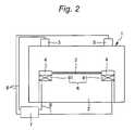
- FIG. 2is a conceptual diagram for illustrating a plasma etching apparatus and a plasma etching method according to a second embodiment of the present invention.
- the drive mechanism 6has a function to change the height of the upper surface of the focus ring 4 at a plurality of locations.
- the drive mechanism 6is composed of a plurality of drive units 61 .
- Each drive unit 61is connected to the controller 7 through the signal cable 8 , and independently drives the focus ring 4 vertically on the basis of individual control signals inputted from the controller 7 .
- the plurality of sensors 5measure the height of the upper surface of the focus ring 4 at a plurality of locations, and output the result of measurement to the controller 7 respectively.
- the height of the upper surface of the focus ring 4is adjusted to the desired position.
- the height of the upper surface of the focus ring 4can be maintained constant at a plurality of locations.
- the location of installationis not limited thereto.
- the number of the sensors 5can be installed on the side of the etching chamber 1 .
- the height of the upper surface of the focus ring 4 at a plurality of locationsmay be measured by allowing a single sensor 5 to scan sequentially without providing a plurality of sensors 5 .
- the scanning of the sensor 5is controlled by the controller 7 .
- the drive mechanism 6is not limited to the mechanism composed of a plurality of drive units 61 as described above, but it may be, for example, an integral mechanism to be supported at three points and to adjust the surface to support the focus ring 4 to desired angle and height.
- the height of the upper surface of the focus ringcan be maintained constant without replacing any focus ring. Therefore, the etching rate at the circumferential portion of the semiconductor substrate can be maintained constant.
Landscapes
- Engineering & Computer Science (AREA)
- Physics & Mathematics (AREA)
- Plasma & Fusion (AREA)
- Chemical & Material Sciences (AREA)
- Analytical Chemistry (AREA)
- Condensed Matter Physics & Semiconductors (AREA)
- General Physics & Mathematics (AREA)
- Manufacturing & Machinery (AREA)
- Computer Hardware Design (AREA)
- Microelectronics & Electronic Packaging (AREA)
- Power Engineering (AREA)
- Drying Of Semiconductors (AREA)
Abstract
Description
Claims (6)
Applications Claiming Priority (2)
| Application Number | Priority Date | Filing Date | Title |
|---|---|---|---|
| JP2000-372798 | 2000-12-07 | ||
| JP2000372798AJP3388228B2 (en) | 2000-12-07 | 2000-12-07 | Plasma etching apparatus and plasma etching method |
Publications (2)
| Publication Number | Publication Date |
|---|---|
| US20020072240A1 US20020072240A1 (en) | 2002-06-13 |
| US6726799B2true US6726799B2 (en) | 2004-04-27 |
Family
ID=18842280
Family Applications (1)
| Application Number | Title | Priority Date | Filing Date |
|---|---|---|---|
| US09/986,044Expired - Fee RelatedUS6726799B2 (en) | 2000-12-07 | 2001-11-07 | Plasma etching apparatus with focus ring and plasma etching method |
Country Status (3)
| Country | Link |
|---|---|
| US (1) | US6726799B2 (en) |
| JP (1) | JP3388228B2 (en) |
| KR (1) | KR100846940B1 (en) |
Cited By (10)
| Publication number | Priority date | Publication date | Assignee | Title |
|---|---|---|---|---|
| US20040083975A1 (en)* | 2002-09-20 | 2004-05-06 | Lam Research Corporation | Apparatus for reducing polymer deposition on a substrate and substrate support |
| US20050103275A1 (en)* | 2003-02-07 | 2005-05-19 | Tokyo Electron Limited | Plasma processing apparatus, ring member and plasma processing method |
| US20070111339A1 (en)* | 2005-11-14 | 2007-05-17 | Stephan Wege | Apparatus for processing a substrate |
| US20090000552A1 (en)* | 2007-06-29 | 2009-01-01 | Hiroshi Sohda | Substrate holder and vacuum film deposition apparatus |
| US20110054661A1 (en)* | 2009-09-01 | 2011-03-03 | Rasnick John W | Direct drive arrangement to control confinement rings positioning and methods thereof |
| WO2012139997A1 (en) | 2011-04-11 | 2012-10-18 | Quadrant Epp Ag | Process for plasma treatment employing ceramic-filled polymer composite parts |
| EP2525387A1 (en) | 2011-05-17 | 2012-11-21 | Quadrant Epp Ag | Process for plasma treatment employing ceramic-filled polyamideimide composite parts |
| US20180190475A1 (en)* | 2017-01-04 | 2018-07-05 | Samsung Electronics Co., Ltd. | Focus ring and plasma-processing apparatus including the same |
| US10600653B2 (en) | 2018-02-23 | 2020-03-24 | Samsung Electronics Co., Ltd. | Method for forming a fine pattern |
| TWI793180B (en)* | 2017-10-11 | 2023-02-21 | 日商東京威力科創股份有限公司 | Plasma processing apparatus, and method and program for controlling elevation of focus ring |
Families Citing this family (59)
| Publication number | Priority date | Publication date | Assignee | Title |
|---|---|---|---|---|
| JP2004071755A (en)* | 2002-08-05 | 2004-03-04 | Matsushita Electric Ind Co Ltd | Plasma processing method and plasma processing apparatus |
| US6896765B2 (en)* | 2002-09-18 | 2005-05-24 | Lam Research Corporation | Method and apparatus for the compensation of edge ring wear in a plasma processing chamber |
| US7311784B2 (en)* | 2002-11-26 | 2007-12-25 | Tokyo Electron Limited | Plasma processing device |
| US6894769B2 (en)* | 2002-12-31 | 2005-05-17 | Tokyo Electron Limited | Monitoring erosion of system components by optical emission |
| US6806949B2 (en)* | 2002-12-31 | 2004-10-19 | Tokyo Electron Limited | Monitoring material buildup on system components by optical emission |
| US7001482B2 (en)* | 2003-11-12 | 2006-02-21 | Tokyo Electron Limited | Method and apparatus for improved focus ring |
| JP4365226B2 (en)* | 2004-01-14 | 2009-11-18 | 株式会社日立ハイテクノロジーズ | Plasma etching apparatus and method |
| US7233878B2 (en)* | 2004-01-30 | 2007-06-19 | Tokyo Electron Limited | Method and system for monitoring component consumption |
| US20080250486A1 (en)* | 2006-10-02 | 2008-10-09 | Gibson Gregg K | Design structure for local blade server security |
| JP5317424B2 (en)* | 2007-03-28 | 2013-10-16 | 東京エレクトロン株式会社 | Plasma processing equipment |
| US8563619B2 (en) | 2007-06-28 | 2013-10-22 | Lam Research Corporation | Methods and arrangements for plasma processing system with tunable capacitance |
| KR100974014B1 (en) | 2008-06-16 | 2010-08-05 | 에이피시스템 주식회사 | Wafer support device and support method |
| WO2015099892A1 (en)* | 2013-12-23 | 2015-07-02 | Applied Materials, Inc. | Extreme edge and skew control in icp plasma reactor |
| US11605546B2 (en)* | 2015-01-16 | 2023-03-14 | Lam Research Corporation | Moveable edge coupling ring for edge process control during semiconductor wafer processing |
| US10658222B2 (en)* | 2015-01-16 | 2020-05-19 | Lam Research Corporation | Moveable edge coupling ring for edge process control during semiconductor wafer processing |
| US10957561B2 (en) | 2015-07-30 | 2021-03-23 | Lam Research Corporation | Gas delivery system |
| US10985078B2 (en)* | 2015-11-06 | 2021-04-20 | Lam Research Corporation | Sensor and adjuster for a consumable |
| US10825659B2 (en) | 2016-01-07 | 2020-11-03 | Lam Research Corporation | Substrate processing chamber including multiple gas injection points and dual injector |
| CN108369922B (en) | 2016-01-26 | 2023-03-21 | 应用材料公司 | Wafer edge ring lifting solution |
| CN116110846A (en) | 2016-01-26 | 2023-05-12 | 应用材料公司 | Wafer edge ring lift solution |
| US10651015B2 (en) | 2016-02-12 | 2020-05-12 | Lam Research Corporation | Variable depth edge ring for etch uniformity control |
| US10699878B2 (en) | 2016-02-12 | 2020-06-30 | Lam Research Corporation | Chamber member of a plasma source and pedestal with radially outward positioned lift pins for translation of a substrate c-ring |
| US10438833B2 (en) | 2016-02-16 | 2019-10-08 | Lam Research Corporation | Wafer lift ring system for wafer transfer |
| US11011353B2 (en) | 2016-03-29 | 2021-05-18 | Lam Research Corporation | Systems and methods for performing edge ring characterization |
| US10312121B2 (en) | 2016-03-29 | 2019-06-04 | Lam Research Corporation | Systems and methods for aligning measurement device in substrate processing systems |
| JP6635888B2 (en)* | 2016-07-14 | 2020-01-29 | 東京エレクトロン株式会社 | Plasma processing system |
| US10410832B2 (en) | 2016-08-19 | 2019-09-10 | Lam Research Corporation | Control of on-wafer CD uniformity with movable edge ring and gas injection adjustment |
| US10510516B2 (en) | 2016-11-29 | 2019-12-17 | Taiwan Semiconductor Manufacturing Company, Ltd. | Moving focus ring for plasma etcher |
| JP6812224B2 (en) | 2016-12-08 | 2021-01-13 | 東京エレクトロン株式会社 | Board processing equipment and mounting table |
| US9947517B1 (en)* | 2016-12-16 | 2018-04-17 | Applied Materials, Inc. | Adjustable extended electrode for edge uniformity control |
| US10553404B2 (en) | 2017-02-01 | 2020-02-04 | Applied Materials, Inc. | Adjustable extended electrode for edge uniformity control |
| TWI843457B (en)* | 2017-04-26 | 2024-05-21 | 日商東京威力科創股份有限公司 | Plasma processing apparatus |
| JP7033926B2 (en)* | 2017-04-26 | 2022-03-11 | 東京エレクトロン株式会社 | Plasma processing equipment |
| KR102387979B1 (en)* | 2017-08-01 | 2022-04-18 | 삼성전자주식회사 | Plasma apparatus |
| US11075105B2 (en) | 2017-09-21 | 2021-07-27 | Applied Materials, Inc. | In-situ apparatus for semiconductor process module |
| CN118380371A (en) | 2017-11-21 | 2024-07-23 | 朗姆研究公司 | Bottom edge ring and middle edge ring |
| KR102693246B1 (en)* | 2017-12-05 | 2024-08-07 | 램 리써치 코포레이션 | System and method for edge ring wear compensation |
| JP7055054B2 (en) | 2018-04-11 | 2022-04-15 | 東京エレクトロン株式会社 | Plasma processing equipment, plasma control method, and plasma control program |
| JP7170422B2 (en)* | 2018-05-15 | 2022-11-14 | 東京エレクトロン株式会社 | processing equipment |
| JP7138474B2 (en)* | 2018-05-15 | 2022-09-16 | 東京エレクトロン株式会社 | Parts repair method and substrate processing system |
| US10600623B2 (en) | 2018-05-28 | 2020-03-24 | Applied Materials, Inc. | Process kit with adjustable tuning ring for edge uniformity control |
| US11935773B2 (en) | 2018-06-14 | 2024-03-19 | Applied Materials, Inc. | Calibration jig and calibration method |
| JP7250449B2 (en)* | 2018-07-04 | 2023-04-03 | 東京エレクトロン株式会社 | Plasma etching method and plasma etching apparatus |
| CN111312633A (en)* | 2018-07-27 | 2020-06-19 | 上海华力集成电路制造有限公司 | Silicon etching machine and operation method thereof |
| US11521872B2 (en)* | 2018-09-04 | 2022-12-06 | Applied Materials, Inc. | Method and apparatus for measuring erosion and calibrating position for a moving process kit |
| JP7076351B2 (en) | 2018-10-03 | 2022-05-27 | 東京エレクトロン株式会社 | Plasma processing device and ring member thickness measurement method |
| JP7129307B2 (en)* | 2018-10-10 | 2022-09-01 | 東京エレクトロン株式会社 | Substrate support assembly, plasma processing apparatus, and plasma processing method |
| JP2020087969A (en)* | 2018-11-15 | 2020-06-04 | 東京エレクトロン株式会社 | Plasma processing apparatus, and method of measuring shape of ring member |
| US11289310B2 (en) | 2018-11-21 | 2022-03-29 | Applied Materials, Inc. | Circuits for edge ring control in shaped DC pulsed plasma process device |
| US10903050B2 (en)* | 2018-12-10 | 2021-01-26 | Lam Research Corporation | Endpoint sensor based control including adjustment of an edge ring parameter for each substrate processed to maintain etch rate uniformity |
| JP2020115499A (en) | 2019-01-17 | 2020-07-30 | 東京エレクトロン株式会社 | Plasma processing apparatus and ring member position deviation measuring method |
| US12009236B2 (en) | 2019-04-22 | 2024-06-11 | Applied Materials, Inc. | Sensors and system for in-situ edge ring erosion monitor |
| JP2021027152A (en)* | 2019-08-05 | 2021-02-22 | キオクシア株式会社 | Plasma processing apparatus and plasma processing method |
| US11443923B2 (en)* | 2019-09-25 | 2022-09-13 | Taiwan Semiconductor Manufacturing Company Ltd. | Apparatus for fabricating a semiconductor structure and method of fabricating a semiconductor structure |
| CN113451191B (en)* | 2020-06-17 | 2022-11-11 | 重庆康佳光电技术研究院有限公司 | Positioning device and etching device |
| KR102585286B1 (en)* | 2020-10-15 | 2023-10-05 | 세메스 주식회사 | Apparatus for treating substrate and mesuring method of consumable component |
| US12315703B2 (en) | 2020-11-26 | 2025-05-27 | Samsung Electronics Co., Ltd. | Plasma processing apparatus and methods of manufacturing semiconductor device using the same |
| CN114639582B (en)* | 2020-12-15 | 2025-02-14 | 中微半导体设备(上海)股份有限公司 | Edge ring height measurement device and method |
| US12205844B2 (en)* | 2021-04-08 | 2025-01-21 | Taiwan Semiconductor Manufacturing Company, Ltd. | Plasma control method in semiconductor wafer fabrication |
Citations (4)
| Publication number | Priority date | Publication date | Assignee | Title |
|---|---|---|---|---|
| JPH04162623A (en) | 1990-10-26 | 1992-06-08 | Mitsubishi Electric Corp | Method and apparatus for plasma treatment |
| JPH1092796A (en) | 1996-09-10 | 1998-04-10 | Tokyo Electron Ltd | Plasma treatment device |
| US6228563B1 (en)* | 1999-09-17 | 2001-05-08 | Gasonics International Corporation | Method and apparatus for removing post-etch residues and other adherent matrices |
| JP2001230239A (en) | 2000-02-15 | 2001-08-24 | Tokyo Electron Ltd | Apparatus and method for treating |
- 2000
- 2000-12-07JPJP2000372798Apatent/JP3388228B2/ennot_activeExpired - Fee Related
- 2001
- 2001-09-25KRKR1020010059190Apatent/KR100846940B1/ennot_activeExpired - Fee Related
- 2001-11-07USUS09/986,044patent/US6726799B2/ennot_activeExpired - Fee Related
Patent Citations (5)
| Publication number | Priority date | Publication date | Assignee | Title |
|---|---|---|---|---|
| JPH04162623A (en) | 1990-10-26 | 1992-06-08 | Mitsubishi Electric Corp | Method and apparatus for plasma treatment |
| US5213658A (en)* | 1990-10-26 | 1993-05-25 | Mitsubishi Denki Kabushiki Kaisha | Plasma processing method |
| JPH1092796A (en) | 1996-09-10 | 1998-04-10 | Tokyo Electron Ltd | Plasma treatment device |
| US6228563B1 (en)* | 1999-09-17 | 2001-05-08 | Gasonics International Corporation | Method and apparatus for removing post-etch residues and other adherent matrices |
| JP2001230239A (en) | 2000-02-15 | 2001-08-24 | Tokyo Electron Ltd | Apparatus and method for treating |
Cited By (21)
| Publication number | Priority date | Publication date | Assignee | Title |
|---|---|---|---|---|
| US7252738B2 (en)* | 2002-09-20 | 2007-08-07 | Lam Research Corporation | Apparatus for reducing polymer deposition on a substrate and substrate support |
| US20080041820A1 (en)* | 2002-09-20 | 2008-02-21 | Lam Research Corporation | Apparatus for reducing polymer deposition on a substrate and substrate support |
| US20040083975A1 (en)* | 2002-09-20 | 2004-05-06 | Lam Research Corporation | Apparatus for reducing polymer deposition on a substrate and substrate support |
| US7867356B2 (en) | 2002-09-20 | 2011-01-11 | Lam Research Corporation | Apparatus for reducing polymer deposition on a substrate and substrate support |
| US8043971B2 (en) | 2003-02-07 | 2011-10-25 | Tokyo Electron Limited | Plasma processing apparatus, ring member and plasma processing method |
| US20050103275A1 (en)* | 2003-02-07 | 2005-05-19 | Tokyo Electron Limited | Plasma processing apparatus, ring member and plasma processing method |
| US20090104781A1 (en)* | 2003-02-07 | 2009-04-23 | Tokyo Electron Limited | Plasma processing apparatus, ring member and plasma processing method |
| US20070111339A1 (en)* | 2005-11-14 | 2007-05-17 | Stephan Wege | Apparatus for processing a substrate |
| US7544270B2 (en)* | 2005-11-14 | 2009-06-09 | Infineon Technologies Ag | Apparatus for processing a substrate |
| US20090000552A1 (en)* | 2007-06-29 | 2009-01-01 | Hiroshi Sohda | Substrate holder and vacuum film deposition apparatus |
| US20110054661A1 (en)* | 2009-09-01 | 2011-03-03 | Rasnick John W | Direct drive arrangement to control confinement rings positioning and methods thereof |
| US8992722B2 (en)* | 2009-09-01 | 2015-03-31 | Lam Research Corporation | Direct drive arrangement to control confinement rings positioning and methods thereof |
| WO2012139997A1 (en) | 2011-04-11 | 2012-10-18 | Quadrant Epp Ag | Process for plasma treatment employing ceramic-filled polymer composite parts |
| US9129795B2 (en) | 2011-04-11 | 2015-09-08 | Quadrant Epp Ag | Process for plasma treatment employing ceramic-filled polyamideimide composite parts |
| US9640381B2 (en) | 2011-04-11 | 2017-05-02 | Quadrant Epp Ag | Process for plasma treatment employing ceramic-filled polymer composite parts |
| EP2525387A1 (en) | 2011-05-17 | 2012-11-21 | Quadrant Epp Ag | Process for plasma treatment employing ceramic-filled polyamideimide composite parts |
| US20180190475A1 (en)* | 2017-01-04 | 2018-07-05 | Samsung Electronics Co., Ltd. | Focus ring and plasma-processing apparatus including the same |
| US10600622B2 (en)* | 2017-01-04 | 2020-03-24 | Samusung Electronics Co., Ltd. | Focus ring with uneven pattern and plasma-processing apparatus including the same |
| TWI793180B (en)* | 2017-10-11 | 2023-02-21 | 日商東京威力科創股份有限公司 | Plasma processing apparatus, and method and program for controlling elevation of focus ring |
| US12315704B2 (en)* | 2017-10-11 | 2025-05-27 | Tokyo Electron Limited | Plasma processing apparatus, and method and program for controlling elevation of focus ring |
| US10600653B2 (en) | 2018-02-23 | 2020-03-24 | Samsung Electronics Co., Ltd. | Method for forming a fine pattern |
Also Published As
| Publication number | Publication date |
|---|---|
| KR100846940B1 (en) | 2008-07-17 |
| US20020072240A1 (en) | 2002-06-13 |
| JP2002176030A (en) | 2002-06-21 |
| KR20020045506A (en) | 2002-06-19 |
| JP3388228B2 (en) | 2003-03-17 |
Similar Documents
| Publication | Publication Date | Title |
|---|---|---|
| US6726799B2 (en) | Plasma etching apparatus with focus ring and plasma etching method | |
| EP1599891B1 (en) | Critical dimension variation compensation across a wafer by means of local wafer temperature control | |
| US6778377B2 (en) | Electrostatic chucking system, and apparatus and method of manufacturing a semiconductor device using the electrostatic chucking system | |
| US6192898B1 (en) | Method and apparatus for cleaning a chamber | |
| US8426317B2 (en) | Plasma processing apparatus and plasma processing method | |
| US8383000B2 (en) | Substrate processing apparatus, method for measuring distance between electrodes, and storage medium storing program | |
| KR20170014384A (en) | Dry etching apparatus | |
| TWI788356B (en) | Detection system for tunable/replaceable edge coupling ring | |
| KR20210002175A (en) | Sensor module and etching apparatus having the same | |
| US8123901B2 (en) | Etching apparatus | |
| JP7682911B2 (en) | Adjusting voltage set points in pulsed RF signals for adjustable edge sheath systems - Patents.com | |
| KR20210011837A (en) | Wafer processing apparatus, and wafer processing method using the same | |
| CN115595555A (en) | Substrate processing apparatus, semiconductor device manufacturing method, and recording medium | |
| JPH04213818A (en) | Cvd device | |
| US20210118685A1 (en) | Plasma processing device and method of adjusting an edge ring of a plasma processing device | |
| KR100301069B1 (en) | Method and apparatus for etching semiconductor wafer | |
| JPH10280173A (en) | Etching method and etching apparatus | |
| KR20200060137A (en) | Device for adjusting height of focus ring, and apparatus for etching wafer with the device | |
| TW202503970A (en) | Adjustable edge ring tilt for edge of wafer skew compensation | |
| KR102707273B1 (en) | Apparatus for semiconductor process | |
| KR100491241B1 (en) | Single wafer type semiconductor manufacturing System for high temperature processes | |
| CN111312633A (en) | Silicon etching machine and operation method thereof | |
| CN120072741A (en) | Wafer clamping device and chuck equipment | |
| JPH11186249A (en) | Semiconductor process control device and control method | |
| JP2004071755A (en) | Plasma processing method and plasma processing apparatus |
Legal Events
| Date | Code | Title | Description |
|---|---|---|---|
| AS | Assignment | Owner name:SEMICONDUCTOR LEADING EDGE TECHNOLOGIES, INC., JAP Free format text:ASSIGNMENT OF ASSIGNORS INTEREST;ASSIGNOR:KOIKE, OSAMU;REEL/FRAME:012299/0836 Effective date:20010913 | |
| AS | Assignment | Owner name:OKI ELECTRIC INDUSTRY CO., LTD., JAPAN Free format text:ASSIGNMENT OF ASSIGNORS INTEREST;ASSIGNOR:SEMICONDUCTOR LEADING EDGE TECHNOLOGIES, INC.;REEL/FRAME:016432/0686 Effective date:20050524 | |
| FPAY | Fee payment | Year of fee payment:4 | |
| FEPP | Fee payment procedure | Free format text:PAYOR NUMBER ASSIGNED (ORIGINAL EVENT CODE: ASPN); ENTITY STATUS OF PATENT OWNER: LARGE ENTITY | |
| AS | Assignment | Owner name:OKI SEMICONDUCTOR CO., LTD., JAPAN Free format text:CHANGE OF NAME;ASSIGNOR:OKI ELECTRIC INDUSTRY CO., LTD.;REEL/FRAME:022162/0669 Effective date:20081001 Owner name:OKI SEMICONDUCTOR CO., LTD.,JAPAN Free format text:CHANGE OF NAME;ASSIGNOR:OKI ELECTRIC INDUSTRY CO., LTD.;REEL/FRAME:022162/0669 Effective date:20081001 | |
| REMI | Maintenance fee reminder mailed | ||
| LAPS | Lapse for failure to pay maintenance fees | ||
| STCH | Information on status: patent discontinuation | Free format text:PATENT EXPIRED DUE TO NONPAYMENT OF MAINTENANCE FEES UNDER 37 CFR 1.362 | |
| FP | Lapsed due to failure to pay maintenance fee | Effective date:20120427 |